observation of the diffraction of a helium-neon laser beam
TRANSCRIPT
HAL Id: hal-00002726https://hal.archives-ouvertes.fr/hal-00002726
Submitted on 5 Sep 2014
HAL is a multi-disciplinary open accessarchive for the deposit and dissemination of sci-entific research documents, whether they are pub-lished or not. The documents may come fromteaching and research institutions in France orabroad, or from public or private research centers.
L’archive ouverte pluridisciplinaire HAL, estdestinée au dépôt et à la diffusion de documentsscientifiques de niveau recherche, publiés ou non,émanant des établissements d’enseignement et derecherche français ou étrangers, des laboratoirespublics ou privés.
Observation of the diffraction of a helium-neon laserbeam on the monoatomic steps of a vicinal sapphire
surfaceMichel Lintz, Marie-Anne Bouchiat
To cite this version:Michel Lintz, Marie-Anne Bouchiat. Observation of the diffraction of a helium-neon laser beam on themonoatomic steps of a vicinal sapphire surface. Surface Science, Elsevier, 2002, 511, pp.L319-L324.�10.1016/S0039-6028(02)01569-8�. �hal-00002726�
1
Observation of the diffraction of a Helium-Neon laser beam
on the monoatomic steps of a vicinal sapphire surface
Michel Lintz1 and Marie-Anne Bouchiat
Laboratoire Kastler-Brossel2
24 rue Lhomond
F 75231 Paris cedex 05
Abstract
"Vicinal" surfaces, with equally spaced monoatomic steps, can be obtained by thermally
annealing single-crystals of materials like sapphire or silicon. We have observed the
diffraction of a Helium-Neon laser beam on the monoatomic steps of a (0001) vicinal
sapphire wafer surface. Diffraction angles were in the range 40° to 50°, in agreement with
the AFM-measured terrace length. Both sides of the wafer gave rise to lowest-order
diffracted beams. This method allows one to determine surface characteristics such as
the direction, average length and regularity of the terraces on the area illuminated by the
laser. In the tested sample the direction of the crystal C axis could be shown to be uniform
to within 5 arc seconds over a 12 mm area of the sample.
Keywords: Surface structure, morphology, roughness and topography; Light scattering;
Vicinal single-crystal surfaces; Aluminium oxide
___________________________________________________________________
1 Corresponding author. Fax: +(33) 1 44 32 34 34; E-mail: [email protected] 2 Affiliated to Ecole Normale Supérieure, Centre National de la Recherche Scientifique (UMR 8552), and Université Pierre et Marie Curie

2
Sapphire (α-Al2O3 single crystal), and more particularly the (0001) surface is a
widely used substrate for the epitaxial growth of metal or semiconductor thin films, or for
silicon-on-sapphire technology. For many of these applications, the surface morphology
can influence the quality of the semiconductor devices obtained. High temperature
annealing of a sapphire surface is known to rearrange partly the originally disordered
surface: it leads to a more or less perfect staircase of monoatomic steps, called a "vicinal
surface" [1]. Steps at sapphire surfaces have been evidenced by reflection electron
microscopy [2]. Later, monoatomic steps were studied in more detail using Scanning
Probe Microscopies (SPM) like AFM (Atomic Force Microscopy) [3,4] or STM (Scanning
Tunnelling Microscopy).
The resolution of SPM techniques allows atomic resolution imaging, and is
invaluable: it has triggered the emergence of conceptually new fields in surface science.
However, since the probe has to scan every point on the surface under scrutiny, these
techniques are inherently slow. Even if the limited range (typically a few microns) of the
piezo actuators used to translate the probe on the surface can be overcome at the
expense of processing data corresponding to different scans, the maximum surface
scanned is basically limited by the time required to scan the probe. Surface control of a
full wafer is not compatible with the scanning probe microscopy throughput. Nor is the
measurement of the roughness of a buried interface.
The very well-known technique of X-ray diffraction has reached a degree of sophistication
which allows some surface parameters, including the terrace length, to be extracted from
grazing-incidence X-ray diffraction measurements [5]. However, the corresponding
diffracted intensities are very low, and experiments can only be performed using high
quality X-ray sources available at synchrotrons.
3
None of these techniques is a natural candidate for on-line inspection of large surfaces
like wafers. Instead, one might prefer a holographic method using a coherent laser beam,
in order to scan simultaneously the different points of a chosen area. Some difficulties can
be foreseen:
- the light intensity diffracted from monoatomic structures is very small: for a
Helium-Neon beam (wavelength λ = 633nm) diffracted on sapphire (index n = 1.8 and
steps of height d = 2.2 Å), one obtains [(d/λ) x (n-1)/(n+1)]2 ≈ 10-8
- while the use of visible light would offer the advantage and simplicity of visual
observation, structures with typical transverse size smaller than the laser wavelength
escape observation
- Light is scattered in all directions of space, which means that detection must be
scanned in all directions, not unlike the AFM or STM probe.
However vicinal surfaces are a particular case, because light diffracted on the more or less
regular grating of the monoatomic terraces is distributed around a given direction of space.
Detection, either by a CCD camera or by visual observation, is made easier due to the
limited solid angle and the correspondingly enhanced intensity. Moreover, the requirement
of a laser wavelength shorter than the terrace length to be detected is less of a problem
due to the increasing number of applications that require long terraces, of several hundred
nanometers, and to the progress in laser diode technology. Commercially available Nichia
blue laser diodes operate at 405nm, while even shorter wavelengths are available via
frequency doubling.
In this letter we report on the observation of the diffraction of a 1mW Helium-Neon laser
beam from the monoatomic terraces of a vicinal sapphire (0001) surface, as a first step
towards holographic mapping of a vicinal surface.
4
Experiment:
We used 25mm diameter (0001) sapphire wafers made by Kyocera3. These 0.5 mm thick
wafers are superpolished on both sides (RMS roughness of a few Ångströms), with a
parallelism of typically 100 microradian (for diagnosis of the parallelism, see for instance
[6]). The miscut angle is specified by Kyocera not to exceed 10 arc minutes, but can be
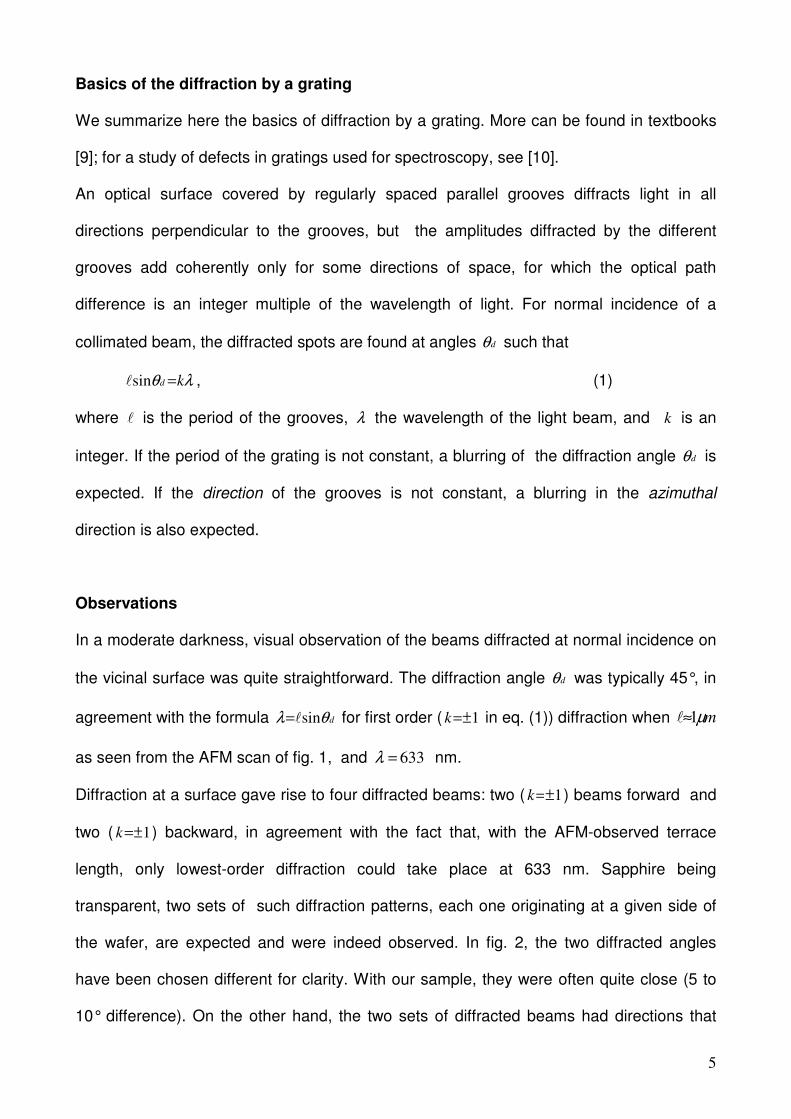
much smaller. Out of a batch of three wafers that were annealed at 1100° C for 1hour,
and then AFM tested, one was observed to have terraces of roughly 1µm length and 2.2 Å
step height (fig 1), which corresponds to a cut angle of approximately 1 arc minute, while
the others had a terrace length shorter than 0.4 µm. The former wafer allowed observation
of diffraction of a 633nm laser beam at normal incidence, while the latter with short terrace
length did not. Nor did wafers that had not been annealed. The He-Ne laser used4 had a
excellent gaussian beam quality (TEM00)5 with 0.6 mm diameter at 1/e² intensity. Use of a
frequency doubled Nd:YAG laser at 532 nm gave qualitatively similar results (except for
the correspondingly smaller diffraction angle) but the beam quality was worse: stray light
was difficult to reject, and the He-Ne laser was preferred.
Observation had to be performed in a clean room, otherwise, within minutes, ambient dust
settling on the wafers soon gave rise to a light scattering level higher than the one due to
diffraction on the monoatomic steps. The experimental set-up is extremely simple (fig. 2)
and inexpensive. Apart from dust, the transmitted and reflected beams were the other
potential source of significant stray light, and had to be completely absorbed. For this
purpose we used beam dumps made of highly absorbing glass plates at Brewster
incidence. As described in [8], the residual light level of these simple laser beam dumps
can easily be made as low as 10-8 or 10-9.
3 Contact: [email protected]; phone: (+33) 1 45 12 02 37; http://www.kyocera.com/kicc/industrial/products/crystal.htm 4 Melles Griot, reference 25 LHP 111. http://www.mellesgriot.com/pdf/0044.4-44.5.pdf 5 For basics of laser physics, see for instance [7]
5
Basics of the diffraction by a grating
We summarize here the basics of diffraction by a grating. More can be found in textbooks
[9]; for a study of defects in gratings used for spectroscopy, see [10].
An optical surface covered by regularly spaced parallel grooves diffracts light in all
directions perpendicular to the grooves, but the amplitudes diffracted by the different
grooves add coherently only for some directions of space, for which the optical path
difference is an integer multiple of the wavelength of light. For normal incidence of a
collimated beam, the diffracted spots are found at angles dθ such that
λθ kd =sinl , (1)
where l is the period of the grooves, λ the wavelength of the light beam, and k is an
integer. If the period of the grating is not constant, a blurring of the diffraction angle dθ is
expected. If the direction of the grooves is not constant, a blurring in the azimuthal
direction is also expected.
Observations
In a moderate darkness, visual observation of the beams diffracted at normal incidence on
the vicinal surface was quite straightforward. The diffraction angle dθ was typically 45°, in
agreement with the formula dθλ sinl= for first order ( 1±=k in eq. (1)) diffraction when mµ1≈l
as seen from the AFM scan of fig. 1, and 633=λ nm.
Diffraction at a surface gave rise to four diffracted beams: two ( 1±=k ) beams forward and
two ( 1±=k ) backward, in agreement with the fact that, with the AFM-observed terrace
length, only lowest-order diffraction could take place at 633 nm. Sapphire being
transparent, two sets of such diffraction patterns, each one originating at a given side of
the wafer, are expected and were indeed observed. In fig. 2, the two diffracted angles
have been chosen different for clarity. With our sample, they were often quite close (5 to
10° difference). On the other hand, the two sets of diffracted beams had directions that
6
differed by a rotation of roughly 30° around the surface normal, indicating that the direction
of the terraces differed by 30° between the upper and lower side. Indeed diffraction was
observed in directions perpendicular to the atomic steps seen on the AFM scans.
Diffraction patterns could be recorded in a Laue-type experiment: a photographic paper,
with two holes to let the beam in and out, was rolled around the wafer in a cylindrical
chamber. A diaphragm, added at the output of the HeNe laser, was needed to remove
most of the fluorescence from the Helium-Neon laser discharge tube. With the 125 ISO
photographic film used, a 5 minute exposure was found to be sufficient. On the unrolled
film (fig. 3), the eight spots are visible. The four spots labelled "1" are rather ellipsoidal and
originate from the same side. The four others, labelled "2", are sharper and more circular;
they correspond to diffraction by the other side of the wafer.
Except for a limited region of the wafer, where only one set of four spots could be
observed, the complete diffraction pattern was observed almost anywhere on the plate.
This confirms that surface reconstruction took place on the whole surface of the plate, on
both sides.
The point-to-point variation of the average diffraction angles indicates the variation of the
terrace length (eq. (1)). On a 12 mm diameter area of the plate the average terrace length
was found to be constant to about ±10%. Variations of the terrace lengths reveal variations
of the cut angle and can originate either i) from an imperfect flatness of the plate, or ii)
from a variation of the crystalline axes. If the crystalline lattice is assumed to be perfect,
and using the 2.2 Å value of the monoatomic step one concludes that surface flatness of
each side of the plate is better than ≈60nm on the considered area. The provider specifies
a (short-scale) surface roughness of a few Ångströms, but not the flatness. Conversely, if
one assumes a perfectly plane surface, then the crystalline axes at two different locations
in this area differ by an angle not exceeding ≈2x10⁻⁵ radian (roughly 5 arc seconds). Since

7
it is unlikely that imperfections in the polishing would exactly compensate for imperfections
in the crystal structure, these figures can be considered as upper limits. In the case of a
thin crystalline sample, one way of discriminating between crystal structure and polishing-
induced variations would be to look for correlated changes in the directions of the two
diffracted beams, since it can be assumed that the crystal axes have the same direction on
both sides of the thin sample.
The last quantity that can be monitored, at a given point on the sample, is the diffracted
intensity distribution, namely its size, shape and structure. While the divergence of the
incident laser beam was 1.35 mradian, diffracted spots were far more divergent, which
suggests that, on the laser beam area, the period and direction of the steps are not
strictly constant. For instance, the divergence of spots #2 in fig. 3 was measured to be ≈5°.
Thus the typical dispersion of the average terrace length on the laser spot can be
estimated to be of ≈±4% of the average6. Finally, let us mention the structure of the
diffraction spots. Fig. 4 shows a photographic recording of one diffraction spot: a 24x36mm
camera without a lens was placed 145mm away from the sample to record the intensity
distribution. The typical size of the "speckle", ≈1.5x10⁻³ radian corresponds to the diameter
of the laser beam (0.6mm at 1/e² intensity) at the sample and contains no information
about the crystal surface, but the intensity distribution is linked to the distribution of the
steps at the surface of the crystal. Whether the actual distribution of the steps can be
obtained from a digital recording of the diffracted intensity distribution is still an open
question. In principle the answer is yes, at least if a holographic method is used, that is, by
adding a reference beam in order to have both amplitude and phase information. This is
an experiment we plan for the near future.
6 Although the correct treatment would require Fourier transformation, an estimate can be made using eq. 1, considering that if diffraction occurs at angle dθ , the corresponding period dθλ sin/=l has to be present on the part of the grating which is illuminated by the laser.

8
After several days in the clean room, some dust settled on the sample, and the surface
had to be cleaned with spectroscopy grade acetone and Kodak cleaning paper. No effect
on diffraction patterns was observed, at least qualitatively, after several such acetone
cleanings. Later, acetone-resistant dust accumulated on the sample, giving rise to a
prohibitive background of scattered light. Etching using 3:1 H3PO4-H2SO4 was decided
(duration 10 mn, temperature 60° C) to clean the sample. After rincing thoroughly with
distilled water, diffraction patterns were still observable.
Conclusion
Diffraction of a 633nm laser beam on the monoatomic steps of a vicinal (0001) sapphire
surface has been observed, revealing the presence of relatively regular terraces on both
sides of the wafer. Characteristics like direction, average length and regularity of the steps
can be obtained with a very unsophisticated apparatus. Unlike scanning probe
microscopies, this optical method allows large size wafers to be scanned in detail.
Extension to magnesium oxide or silicon wafers is straightforward. These results are
encouraging in the view of a holographic method, where the diffracted amplitude and
phase would be recorded numerically and then processed to calculate the distribution of
the steps at the surface.
Acknowledgments: We are grateful to M. G. Battuz and A. Hadj-Azzem (CRTBT,
Grenoble) for the annealing of the substrates, and to V. Bouchiat, for the AFM scans of the
samples, and for his help and interest in this work.
Appendices: (no appendix)

9
References
[1] H. C. Jeong and E. D. Williams, Surf. Sci. Rep. 34(1999)171.
[2] Y. Kim and T. Hsu, Surf. Sci. 258 (1991) 131.
[3] M. Yoshimoto, T. Maeda, T. Ohnishi, H. Koinuma, O. Oshiyama, M. Shinohara, M.
Kubo, R. Miura and A. Miyamoto, Appl. Phys. Lett. 67(1995)2615.
[4] J. R. Heffelfinger, M. W. Bench, C. B. Carter, Surf. Sci. 370(1997)L168.
[5] G. Renaud, Surf. Sci. Rep. 32(1998)1.
[6] E. Jahier, J. Guéna, Ph. Jacquier, M. Lintz, A. V. Papoyan and M. A. Bouchiat, Appl.
Phys. B71 (2000) 561. [7] O. Svelto, Principles of lasers, 4th ed. (Plenum Press, New York, 1998).
[8] M. Lintz. and A. V. Papoyan, Rev. Sci. Instr. 71 (2000) 4681.
[9] M. Born and E. Wolf, Pinciples of optics, 2nd ed. (Pergamon Press, Oxford, 1964)
E. Hecht, A. Zajac, Optics (Addison-Wesley,1974)
[10] G. W. Stroke, in: Progress in Optics, Vol. 2, Ed. E. Wolf , (North Holland, Amsterdam,
1963)
10
FigureFigureFigureFiguressss
Fig 1: Fig 1: Fig 1: Fig 1: AFM scan of the surface of the annealed (1100° C, 1 hour) sapphire wafer used in
the diffraction experiments. Surface scanned : 4µm x 4µm. The observed steps are ≈2.2 Å
high.

11
Fig 2:Fig 2:Fig 2:Fig 2: Experimental set-up. LBDLBDLBDLBD: laser beam dump (described in ref. [8]). SSSS: annealed
sapphire sample. FilmFilmFilmFilm: photographic film inserted in a ∅ 30mm cylindrical chamber, for
photographic recordings of the diffraction pattern. Diaph:Diaph:Diaph:Diaph: diaphragm, to reject
uncollimated fluorescence from the Helium-Neon tube (necessary for photographic
recordings). The four beams numbered "1" (resp. "2") are due to diffraction on the upper
(resp. lower) side of the sample.
Diaph
1 1
1 1
2
2 2
2
LBD
Film
LBD
S
HeNe laser

12
Fig 3:Fig 3:Fig 3:Fig 3: Typical "Laue-type" photographic recording of the diffraction pattern. The sample
was not positioned exactly on the axis of the cylindrical chamber; this explains the
imperfect up-down symmetry of the pattern. Exposure time: 5 mn. Film used: 125 ISO
Ilford FP4 film. White dots: position of the laser beam at the input and output of the
chamber.
1
1 1
1
2 2
2
2

13
Fig 4: Fig 4: Fig 4: Fig 4: Photographic recording of the intensity distribution of a diffracted beam. The 400
ISO film was 145 mm away from the sample. Actual dimensions: 24.5 mm x 19 mm.
Exposure time: 4 mn. The tested wafer area is not the same as in fig. 3.
θθθθd = 40°= 40°= 40°= 40°
θθθθd = 50°= 50°= 50°= 50°