numaker-m2354 user manual
TRANSCRIPT

NuMaker-M2354
Dec. 25, 2020 Page 1 of 54 Rev 1.00
NU
MA
KE
R-M
2354 U
SE
R M
AN
UA
L
Maker N
u-m
bed
NU
C472 U
ser M
an
ual
NuMicro® Family
Based on Arm® Cortex® -M23
NuMaker-M2354
User Manual Evaluation Board for NuMicro® M2354 Series
The information described in this document is the exclusive intellectual property of Nuvoton Technology Corporation and shall not be reproduced without permission from Nuvoton.
Nuvoton is providing this document only for reference purposes of NuMicro microcontroller based system design. Nuvoton assumes no responsibility for errors or omissions.
All data and specifications are subject to change without notice.
For additional information or questions, please contact: Nuvoton Technology Corporation.
www.nuvoton.com

NuMaker-M2354
Dec. 25, 2020 Page 2 of 54 Rev 1.00
NU
MA
KE
R-M
2354 U
SE
R M
AN
UA
L
Maker N
u-m
bed
NU
C472 U
ser M
an
ual
Table of Contents
1 Overview .................................................................................... 7
2 Features .................................................................................... 8
3 Hardware Configuration .................................................................. 9
Front View ...................................................................................... 9
Rear View .....................................................................................10
Extension Connectors .......................................................................11
3.3.1 Pin Assignment for Extension Connectors...................................................... 11
3.3.2 Arduino UNO Compatible Extension Connectors ............................................. 17
Power Supply Configuration ...............................................................19
3.4.1 VIN Power Source .................................................................................. 19
3.4.2 5V Power Sources .................................................................................. 19
3.4.3 3.3 V Power Sources ............................................................................... 19
3.4.4 1.8V Power Sources ............................................................................... 20
3.4.5 Power Connectors .................................................................................. 20
3.4.6 USB Connectors .................................................................................... 20
3.4.7 Power Switches ..................................................................................... 20
3.4.8 Power Supply Models .............................................................................. 21
External Reference Voltage Connector ..................................................24
Ammeter Connector .........................................................................24
Push-Buttons .................................................................................24
MicroSD Card Slot ...........................................................................24
SWD / ETM interface ........................................................................25
LEDs ...........................................................................................25
Wi-Fi Module (ESP-12) .....................................................................25
HTN-LCD Panel ..............................................................................26
Nu-Link2-Me ..................................................................................27
3.13.1 VCOM Switches ..................................................................................... 27
3.13.2 Status LEDs ......................................................................................... 27
4 Quick Start ............................................................................... 28
Toolchains Support ..........................................................................28
Nuvoton Nu-Link Driver Installation .......................................................28
BSP Firmware Download ...................................................................30
Hardware Setup ..............................................................................30

NuMaker-M2354
Dec. 25, 2020 Page 3 of 54 Rev 1.00
NU
MA
KE
R-M
2354 U
SE
R M
AN
UA
L
Maker N
u-m
bed
NU
C472 U
ser M
an
ual
Finding the Example Project ...............................................................32
Executing the Project under Toolchains .................................................32
4.6.1 Keil MDK ............................................................................................. 32
4.6.2 IAR EWARM ......................................................................................... 35
4.6.3 NuEclipse ............................................................................................ 37
5 NuMaker-M2354 Schematics ......................................................... 43
Nu-Link2-Me ..................................................................................43
M2354 target Board .........................................................................44
USB 2.0 FS OTG ............................................................................45
Power Supply .................................................................................46
MCU Connector ..............................................................................47
Arduino UNO Compatible Interface .......................................................48
MicroSD Card ................................................................................49
Wi-Fi Module (ESP-12) .....................................................................50
LCD interface .................................................................................51
PCB Placement ..............................................................................52
6 REVISION HISTORY ................................................................... 53

NuMaker-M2354
Dec. 25, 2020 Page 4 of 54 Rev 1.00
NU
MA
KE
R-M
2354 U
SE
R M
AN
UA
L
Maker N
u-m
bed
NU
C472 U
ser M
an
ual
List of Figures
Figure 1-1 NuMaker-M2354 Board .................................................................................................. 7
Figure 3-1 Front View of NuMaker-M2354 ....................................................................................... 9
Figure 3-2 Rear View of NuMaker-M2354 ..................................................................................... 10
Figure 3-3 M2354 Extension Connectors ...................................................................................... 11
Figure 3-4 Arduino UNO Compatible Extension Connectors ......................................................... 17
Figure 3-5 External Power Supply Sources on Nu-Link2-Me ........................................................ 21
Figure 3-6 External Power Supply Sources on M2354 target board ............................................. 22
Figure 3-7 Separate the Nu-Link2-Me from NuMaker-M2354 ....................................................... 23
Figure 3-8 Wiring between Ammeter Connector and Ammeter ..................................................... 24
Figure 3-9 LCD interface ................................................................................................................ 26
Figure 4-1 Nu-Link USB Driver Installation Setup .......................................................................... 28
Figure 4-2 Nu-Link USB Driver Installation .................................................................................... 29
Figure 4-3 Open VCOM Function .................................................................................................. 30
Figure 4-4 ICE USB Connector ...................................................................................................... 30
Figure 4-5 Device Manger .............................................................................................................. 31
Figure 4-6 PuTTY Session Setting................................................................................................. 31
Figure 4-7 Blinky Project Folder Path ............................................................................................ 32
Figure 4-8 Debugger Setting in Options Window ........................................................................... 32
Figure 4-9 Programming Setting in Options Window ..................................................................... 33
Figure 4-10 Compile and Download the Project ............................................................................ 33
Figure 4-11 Keil MDK Debug Mode ............................................................................................... 34
Figure 4-12 Debug Message on Serial Port Terminal Windows .................................................... 34
Figure 4-13 IAR EWARM Window ................................................................................................. 35
Figure 4-14 Compile and Download the Project ............................................................................ 35
Figure 4-15 IAR EWARM Debug Mode ......................................................................................... 36
Figure 4-16 Debug Message on Serial Port Terminal Windows .................................................... 36
Figure 4-17 Import the Project in NuEclipse .................................................................................. 37
Figure 4-18 Import Projects Windows ............................................................................................ 37
Figure 4-19 Build Project ................................................................................................................ 38
Figure 4-20 Project Properties Settings ......................................................................................... 38
Figure 4-21 Build Project ................................................................................................................ 39
Figure 4-22 Open Debug Configuration ......................................................................................... 39
Figure 4-23 Main Tab Configuration .............................................................................................. 40
Figure 4-24 Debugger Tab Configuration ...................................................................................... 40
Figure 4-25 Startup Tab Configuration .......................................................................................... 41
Figure 4-26 NuEclipse Debug Mode .............................................................................................. 42

NuMaker-M2354
Dec. 25, 2020 Page 5 of 54 Rev 1.00
NU
MA
KE
R-M
2354 U
SE
R M
AN
UA
L
Maker N
u-m
bed
NU
C472 U
ser M
an
ual
Figure 4-27 Debug Message on Serial Port Terminal Windows .................................................... 42
Figure 5-1 Nu-Link2-Me Circuit ...................................................................................................... 43
Figure 5-2 M2354 Pin Assignment ................................................................................................. 44
Figure 5-3 USB 2.0 FS OTG Circuit ............................................................................................... 45
Figure 5-4 Power Circuit and Configurations ................................................................................. 46
Figure 5-5 MCU connector ............................................................................................................. 47
Figure 5-6 Arduino UNO Compatible Interface .............................................................................. 48
Figure 5-7 MicroSD Card Circuit .................................................................................................... 49
Figure 5-8 Wi-Fi Module Circuit ..................................................................................................... 50
Figure 5-9 LCD interface Circuit ..................................................................................................... 51
Figure 5-10 Front Placement ......................................................................................................... 52
Figure 5-11 Rear Placement .......................................................................................................... 52

NuMaker-M2354
Dec. 25, 2020 Page 6 of 54 Rev 1.00
NU
MA
KE
R-M
2354 U
SE
R M
AN
UA
L
Maker N
u-m
bed
NU
C472 U
ser M
an
ual
List of Tables
Table 3-1 Extension Connectors .................................................................................................... 11
Table 3-2 M2354KJFAE Full-pin Extension Connectors and GPIO Function List ......................... 16
Table 3-3 Arduino UNO Extension Connectors and M2354KJFAE Mapping GPIO List ............... 18
Table 3-4 Vin Power Source .......................................................................................................... 19
Table 3-5 5V Power Sources ......................................................................................................... 19
Table 3-6 3.3 V Power Sources ..................................................................................................... 20
Table 3-7 1.8V Power Sources ...................................................................................................... 20
Table 3-8 Power Connectors ......................................................................................................... 20
Table 3-9 USB Connectors ............................................................................................................ 20
Table 3-10 Power Switches ........................................................................................................... 21
Table 3-11 Supply External Power through Nu-Link2-Me ............................................................. 22
Table 3-12 Supply External Power for M2354 target board ........................................................... 23
Table 3-13 External Reference Voltage Connector ....................................................................... 24
Table 3-14 Ammeter Connector ..................................................................................................... 24
Table 3-15 Push-Buttons ............................................................................................................... 24
Table 3-16 LEDs ............................................................................................................................ 25
Table 3-17 Optional Function of ESP-12 ....................................................................................... 25
Table 3-18 VCOM Function of Nu-Link2-Me .................................................................................. 27
Table 3-19 Status LEDs patterns of Nu-Link2-Me ......................................................................... 27

NuMaker-M2354
Dec. 25, 2020 Page 7 of 54 Rev 1.00
NU
MA
KE
R-M
2354 U
SE
R M
AN
UA
L
Maker N
u-m
bed
NU
C472 U
ser M
an
ual
1 OVERVIEW
The NuMaker-M2354 is an evaluation board for Nuvoton NuMicro M2354 microcontrollers. The NuMaker-M2354 consists of two parts, a M2354 target board and an on-board Nu-Link2-Me debugger and programmer. The NuMaker-M2354 is designed for secure evaluation, prototype development and validation with power consumption monitoring function.
The M2354 target board is based on NuMicro M2354KJFAE. For the development flexibility, the M2354 target board provides the extension connectors of M2354KJFAE, the Arduino UNO compatible headers and is able to adopt multiple power supply by external power connectors. Furthermore, the Nuvoton-designed ammeter connector can measure the power consumption instantly, which is essential for the prototype evaluation. The M2354 target board also has Wi-Fi connectivity on board and LCD display panel (COM/SEG) for quick development.
In addition, there is an attached on-board debugger and programmer “Nu-Link2-Me”. The Nu-Link2-Me supports on-chip debugging, online and offline ICP programming via SWD interface. The Nu-Link2-Me supports virtual COM (VCOM) port for printing debug messages on PC. Besides, the programming status could be shown on the built-in LEDs. Lastly, the Nu-Link2-Me could be detached from the evaluation board and become a stand-alone mass production programmer.
Figure 1-1 NuMaker-M2354 Board

NuMaker-M2354
Dec. 25, 2020 Page 8 of 54 Rev 1.00
NU
MA
KE
R-M
2354 U
SE
R M
AN
UA
L
Maker N
u-m
bed
NU
C472 U
ser M
an
ual
2 FEATURES
NuMicro M2354KJFAE microcontroller with function compatible with:
– M2354LJFAE
– M2354SJFAE
M2354KJFAE extension connectors
Arduino UNO compatible extension connectors
COM/SEG LCD with panel
ETM (embedded trace macrocell) debug interface for instruction and data tracing of a processor
Wi-Fi module for wireless application
MicroSD Card slot for T-Flash
Ammeter connector for measuring the microcontroller’s power consumption
Flexible board power supply:
– External VDD power connector
– Arduino UNO compatible extension connector Vin
– USB FS connector on M031 target board
– ICE USB connector on Nu-Link2-Me
On-board Nu-Link2-Me debugger and programmer:
– Debug through SWD interface
– Online/offline programming
– Virtual COM port function
NuMaker-M2354
Dec. 25, 2020 Page 9 of 54 Rev 1.00
NU
MA
KE
R-M
2354 U
SE
R M
AN
UA
L
Maker N
u-m
bed
NU
C472 U
ser M
an
ual
3 HARDWARE CONFIGURATION
Front View
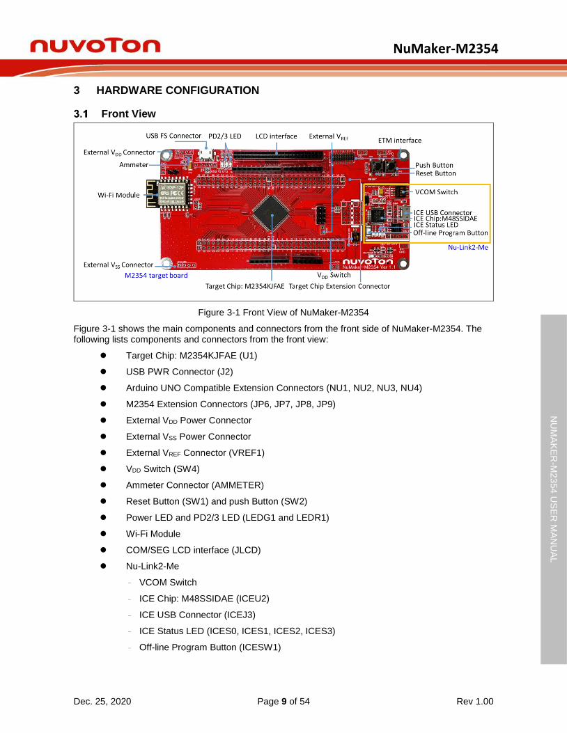
Figure 3-1 Front View of NuMaker-M2354
Figure 3-1 shows the main components and connectors from the front side of NuMaker-M2354. The following lists components and connectors from the front view:
Target Chip: M2354KJFAE (U1)
USB PWR Connector (J2)
Arduino UNO Compatible Extension Connectors (NU1, NU2, NU3, NU4)
M2354 Extension Connectors (JP6, JP7, JP8, JP9)
External VDD Power Connector
External VSS Power Connector
External VREF Connector (VREF1)
VDD Switch (SW4)
Ammeter Connector (AMMETER)
Reset Button (SW1) and push Button (SW2)
Power LED and PD2/3 LED (LEDG1 and LEDR1)
Wi-Fi Module
COM/SEG LCD interface (JLCD)
Nu-Link2-Me
– VCOM Switch
– ICE Chip: M48SSIDAE (ICEU2)
– ICE USB Connector (ICEJ3)
– ICE Status LED (ICES0, ICES1, ICES2, ICES3)
– Off-line Program Button (ICESW1)
NuMaker-M2354
Dec. 25, 2020 Page 10 of 54 Rev 1.00
NU
MA
KE
R-M
2354 U
SE
R M
AN
UA
L
Maker N
u-m
bed
NU
C472 U
ser M
an
ual
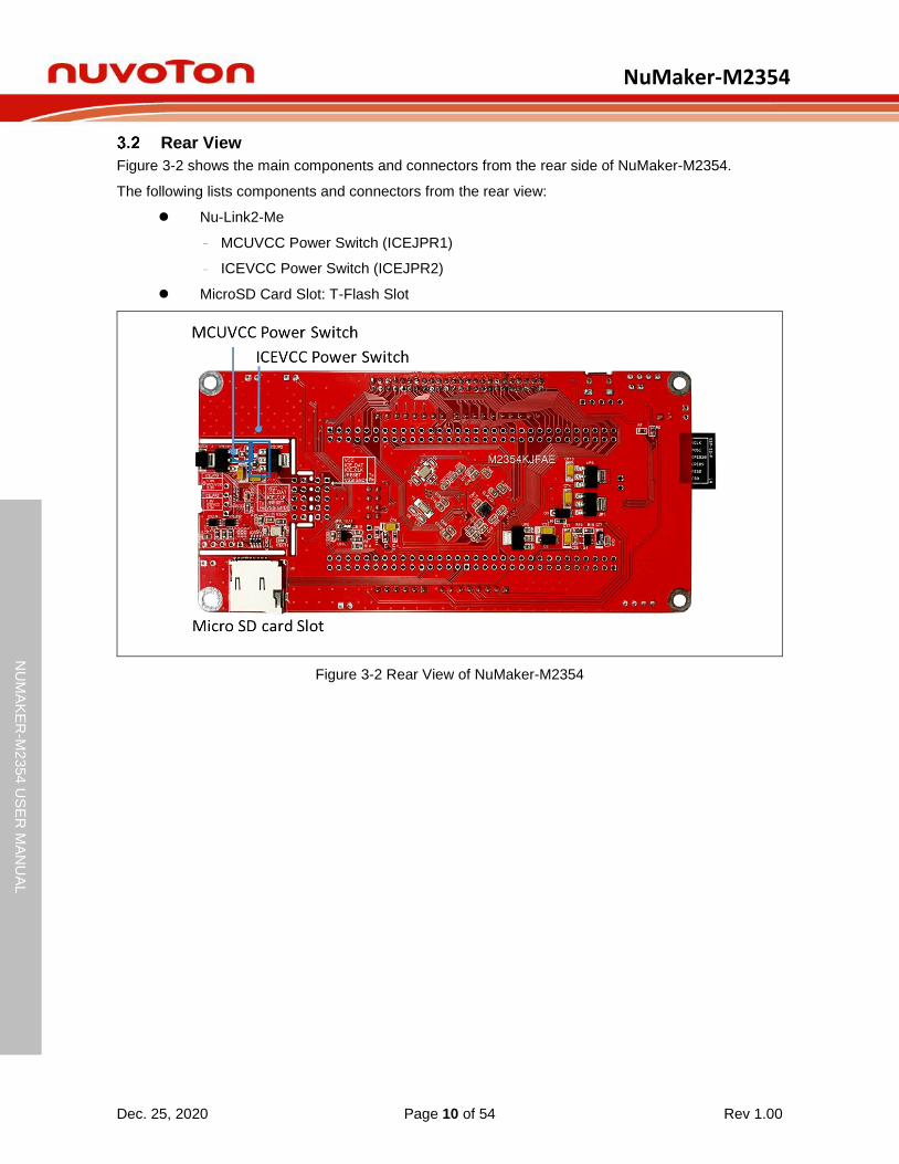
Rear View
Figure 3-2 shows the main components and connectors from the rear side of NuMaker-M2354.
The following lists components and connectors from the rear view:
Nu-Link2-Me
– MCUVCC Power Switch (ICEJPR1)
– ICEVCC Power Switch (ICEJPR2)
MicroSD Card Slot: T-Flash Slot
Figure 3-2 Rear View of NuMaker-M2354

NuMaker-M2354
Dec. 25, 2020 Page 11 of 54 Rev 1.00
NU
MA
KE
R-M
2354 U
SE
R M
AN
UA
L
Maker N
u-m
bed
NU
C472 U
ser M
an
ual
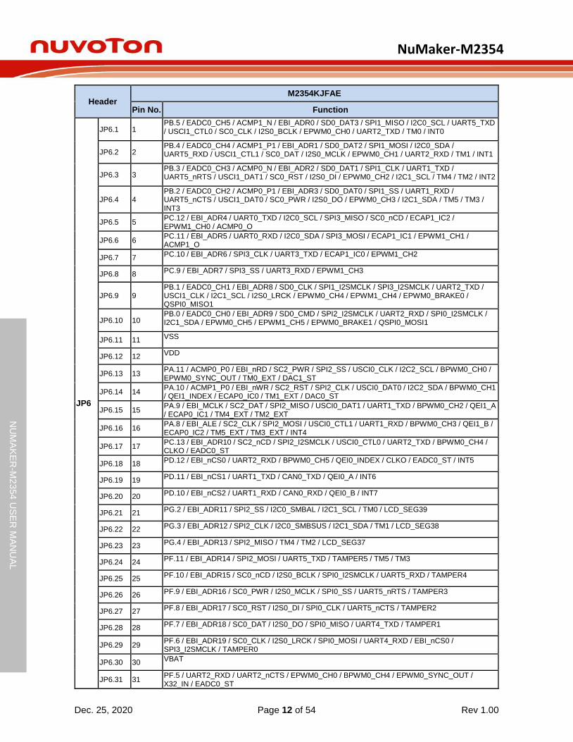
Extension Connectors
Table 3-1 presents the extension connectors.
Connector Description
JP6, JP7, JP8 and JP9 Full pins extension connectors on the NuMaker-M2354.
NU1, NU2, NU3 and NU4
Arduino UNO compatible pins on the NuMaker-M2354.
Table 3-1 Extension Connectors
3.3.1 Pin Assignment for Extension Connectors
The NuMaker-M2354 provides the M2354 target chip on board and full pins extension connectors (JP6, JP7, JP8 and JP9). Figure 3-3 shows the M2354 extension connectors.
JP6Pin1 ~ Pin32
JP9Pin97 ~ Pin128
JP8 Pin33 ~ Pin64
JP7 Pin65 ~ Pin96
Figure 3-3 M2354 Extension Connectors
NuMaker-M2354
Dec. 25, 2020 Page 12 of 54 Rev 1.00
NU
MA
KE
R-M
2354 U
SE
R M
AN
UA
L
Maker N
u-m
bed
NU
C472 U
ser M
an
ual
Header M2354KJFAE
Pin No. Function
JP6
JP6.1 1 PB.5 / EADC0_CH5 / ACMP1_N / EBI_ADR0 / SD0_DAT3 / SPI1_MISO / I2C0_SCL / UART5_TXD / USCI1_CTL0 / SC0_CLK / I2S0_BCLK / EPWM0_CH0 / UART2_TXD / TM0 / INT0
JP6.2 2 PB.4 / EADC0_CH4 / ACMP1_P1 / EBI_ADR1 / SD0_DAT2 / SPI1_MOSI / I2C0_SDA / UART5_RXD / USCI1_CTL1 / SC0_DAT / I2S0_MCLK / EPWM0_CH1 / UART2_RXD / TM1 / INT1
JP6.3 3 PB.3 / EADC0_CH3 / ACMP0_N / EBI_ADR2 / SD0_DAT1 / SPI1_CLK / UART1_TXD / UART5_nRTS / USCI1_DAT1 / SC0_RST / I2S0_DI / EPWM0_CH2 / I2C1_SCL / TM4 / TM2 / INT2
JP6.4 4 PB.2 / EADC0_CH2 / ACMP0_P1 / EBI_ADR3 / SD0_DAT0 / SPI1_SS / UART1_RXD / UART5_nCTS / USCI1_DAT0 / SC0_PWR / I2S0_DO / EPWM0_CH3 / I2C1_SDA / TM5 / TM3 / INT3
JP6.5 5 PC.12 / EBI_ADR4 / UART0_TXD / I2C0_SCL / SPI3_MISO / SC0_nCD / ECAP1_IC2 / EPWM1_CH0 / ACMP0_O
JP6.6 6 PC.11 / EBI_ADR5 / UART0_RXD / I2C0_SDA / SPI3_MOSI / ECAP1_IC1 / EPWM1_CH1 / ACMP1_O
JP6.7 7 PC.10 / EBI_ADR6 / SPI3_CLK / UART3_TXD / ECAP1_IC0 / EPWM1_CH2
JP6.8 8 PC.9 / EBI_ADR7 / SPI3_SS / UART3_RXD / EPWM1_CH3
JP6.9 9 PB.1 / EADC0_CH1 / EBI_ADR8 / SD0_CLK / SPI1_I2SMCLK / SPI3_I2SMCLK / UART2_TXD / USCI1_CLK / I2C1_SCL / I2S0_LRCK / EPWM0_CH4 / EPWM1_CH4 / EPWM0_BRAKE0 / QSPI0_MISO1
JP6.10 10 PB.0 / EADC0_CH0 / EBI_ADR9 / SD0_CMD / SPI2_I2SMCLK / UART2_RXD / SPI0_I2SMCLK / I2C1_SDA / EPWM0_CH5 / EPWM1_CH5 / EPWM0_BRAKE1 / QSPI0_MOSI1
JP6.11 11 VSS
JP6.12 12 VDD
JP6.13 13 PA.11 / ACMP0_P0 / EBI_nRD / SC2_PWR / SPI2_SS / USCI0_CLK / I2C2_SCL / BPWM0_CH0 / EPWM0_SYNC_OUT / TM0_EXT / DAC1_ST
JP6.14 14 PA.10 / ACMP1_P0 / EBI_nWR / SC2_RST / SPI2_CLK / USCI0_DAT0 / I2C2_SDA / BPWM0_CH1 / QEI1_INDEX / ECAP0_IC0 / TM1_EXT / DAC0_ST
JP6.15 15 PA.9 / EBI_MCLK / SC2_DAT / SPI2_MISO / USCI0_DAT1 / UART1_TXD / BPWM0_CH2 / QEI1_A / ECAP0_IC1 / TM4_EXT / TM2_EXT
JP6.16 16 PA.8 / EBI_ALE / SC2_CLK / SPI2_MOSI / USCI0_CTL1 / UART1_RXD / BPWM0_CH3 / QEI1_B / ECAP0_IC2 / TM5_EXT / TM3_EXT / INT4
JP6.17 17 PC.13 / EBI_ADR10 / SC2_nCD / SPI2_I2SMCLK / USCI0_CTL0 / UART2_TXD / BPWM0_CH4 / CLKO / EADC0_ST
JP6.18 18 PD.12 / EBI_nCS0 / UART2_RXD / BPWM0_CH5 / QEI0_INDEX / CLKO / EADC0_ST / INT5
JP6.19 19 PD.11 / EBI_nCS1 / UART1_TXD / CAN0_TXD / QEI0_A / INT6
JP6.20 20 PD.10 / EBI_nCS2 / UART1_RXD / CAN0_RXD / QEI0_B / INT7
JP6.21 21 PG.2 / EBI_ADR11 / SPI2_SS / I2C0_SMBAL / I2C1_SCL / TM0 / LCD_SEG39
JP6.22 22 PG.3 / EBI_ADR12 / SPI2_CLK / I2C0_SMBSUS / I2C1_SDA / TM1 / LCD_SEG38
JP6.23 23 PG.4 / EBI_ADR13 / SPI2_MISO / TM4 / TM2 / LCD_SEG37
JP6.24 24 PF.11 / EBI_ADR14 / SPI2_MOSI / UART5_TXD / TAMPER5 / TM5 / TM3
JP6.25 25 PF.10 / EBI_ADR15 / SC0_nCD / I2S0_BCLK / SPI0_I2SMCLK / UART5_RXD / TAMPER4
JP6.26 26 PF.9 / EBI_ADR16 / SC0_PWR / I2S0_MCLK / SPI0_SS / UART5_nRTS / TAMPER3
JP6.27 27 PF.8 / EBI_ADR17 / SC0_RST / I2S0_DI / SPI0_CLK / UART5_nCTS / TAMPER2
JP6.28 28 PF.7 / EBI_ADR18 / SC0_DAT / I2S0_DO / SPI0_MISO / UART4_TXD / TAMPER1
JP6.29 29 PF.6 / EBI_ADR19 / SC0_CLK / I2S0_LRCK / SPI0_MOSI / UART4_RXD / EBI_nCS0 / SPI3_I2SMCLK / TAMPER0
JP6.30 30 VBAT
JP6.31 31 PF.5 / UART2_RXD / UART2_nCTS / EPWM0_CH0 / BPWM0_CH4 / EPWM0_SYNC_OUT / X32_IN / EADC0_ST

NuMaker-M2354
Dec. 25, 2020 Page 13 of 54 Rev 1.00
NU
MA
KE
R-M
2354 U
SE
R M
AN
UA
L
Maker N
u-m
bed
NU
C472 U
ser M
an
ual
Header M2354KJFAE
Pin No. Function
JP6.32 32 PF.4 / UART2_TXD / UART2_nRTS / EPWM0_CH1 / BPWM0_CH5 / X32_OUT
JP8
JP8.1 33 PH.4 / EBI_ADR3 / SPI1_MISO / LCD_SEG36
JP8.2 34 PH.5 / EBI_ADR2 / SPI1_MOSI / LCD_SEG35
JP8.3 35 PH.6 / EBI_ADR1 / SPI1_CLK / LCD_SEG34
JP8.4 36 PH.7 / EBI_ADR0 / SPI1_SS / LCD_SEG33
JP8.5 37 PF.3 / EBI_nCS0 / UART0_TXD / I2C0_SCL / XT1_IN / BPWM1_CH0
JP8.6 38 PF.2 / EBI_nCS1 / UART0_RXD / I2C0_SDA / QSPI0_CLK / XT1_OUT / BPWM1_CH1
JP8.7 39 VSS
JP8.8 40 VDD
JP8.9 41 PE.8 / EBI_ADR10 / I2S0_BCLK / SPI2_CLK / USCI1_CTL1 / UART2_TXD / EPWM0_CH0 / EPWM0_BRAKE0 / ECAP0_IC0 / TRACE_DATA3 / LCD_SEG32
JP8.10 42 PE.9 / EBI_ADR11 / I2S0_MCLK / SPI2_MISO / USCI1_CTL0 / UART2_RXD / EPWM0_CH1 / EPWM0_BRAKE1 / ECAP0_IC1 / TRACE_DATA2 / LCD_SEG31
JP8.11 43 PE.10 / EBI_ADR12 / I2S0_DI / SPI2_MOSI / USCI1_DAT0 / UART3_TXD / EPWM0_CH2 / EPWM1_BRAKE0 / ECAP0_IC2 / TRACE_DATA1 / LCD_SEG30
JP8.12 44 PE.11 / EBI_ADR13 / I2S0_DO / SPI2_SS / USCI1_DAT1 / UART3_RXD / UART1_nCTS / EPWM0_CH3 / EPWM1_BRAKE1 / ECAP1_IC2 / TRACE_DATA0
JP8.13 45 PE.12 / EBI_ADR14 / I2S0_LRCK / SPI2_I2SMCLK / USCI1_CLK / UART1_nRTS / EPWM0_CH4 / ECAP1_IC1 / TRACE_CLK
JP8.14 46 PE.13 / EBI_ADR15 / I2C0_SCL / UART4_nRTS / UART1_TXD / EPWM0_CH5 / EPWM1_CH0 / BPWM1_CH5 / ECAP1_IC0
JP8.15 47 PC.8 / EBI_ADR16 / I2C0_SDA / UART4_nCTS / UART1_RXD / EPWM1_CH1 / BPWM1_CH4
JP8.16 48 PC.7 / EBI_AD9 / SPI1_MISO / UART4_TXD / SC2_PWR / UART0_nCTS / I2C1_SMBAL / EPWM1_CH2 / BPWM1_CH0 / TM0 / INT3
JP8.17 49 PC.6 / EBI_AD8 / SPI1_MOSI / UART4_RXD / SC2_RST / UART0_nRTS / I2C1_SMBSUS / EPWM1_CH3 / BPWM1_CH1 / TM1 / INT2
JP8.18 50 PA.7 / EBI_AD7 / SPI1_CLK / SC2_DAT / UART0_TXD / I2C1_SCL / TM4 / EPWM1_CH4 / BPWM1_CH2 / ACMP0_WLAT / TM2 / INT1
JP8.19 51 PA.6 / EBI_AD6 / SPI1_SS / SC2_CLK / UART0_RXD / I2C1_SDA / TM5 / EPWM1_CH5 / BPWM1_CH3 / ACMP1_WLAT / TM3 / INT0
JP8.20 52 VSS
JP8.21 53 VDD
JP8.22 54 LDO_CAP
JP8.23 55 PA.5 / QSPI0_MISO1 / SPI1_I2SMCLK / SC2_nCD / UART0_nCTS / UART5_TXD / I2C0_SCL / CAN0_TXD / UART0_TXD / BPWM0_CH5 / EPWM0_CH0 / QEI0_INDEX / LCD_SEG29
JP8.24 56 PA.4 / QSPI0_MOSI1 / SPI0_I2SMCLK / SC0_nCD / UART0_nRTS / UART5_RXD / I2C0_SDA / CAN0_RXD / UART0_RXD / BPWM0_CH4 / EPWM0_CH1 / QEI0_A / LCD_SEG28
JP8.25 57 PA.3 / QSPI0_SS / SPI0_SS / SC0_PWR / UART4_TXD / UART1_TXD / I2C1_SCL / I2C0_SMBAL / LCD_SEG27 / BPWM0_CH3 / EPWM0_CH2 / QEI0_B / EPWM1_BRAKE1
JP8.26 58 PA.2 / QSPI0_CLK / SPI0_CLK / SC0_RST / UART4_RXD / UART1_RXD / I2C1_SDA / I2C0_SMBSUS / LCD_SEG26 / BPWM0_CH2 / EPWM0_CH3
JP8.27 59 PA.1 / QSPI0_MISO0 / SPI0_MISO / SC0_DAT / UART0_TXD / UART1_nCTS / I2C2_SCL / LCD_SEG25 / BPWM0_CH1 / EPWM0_CH4 / DAC1_ST
JP8.28 60 PA.0 / QSPI0_MOSI0 / SPI0_MOSI / SC0_CLK / UART0_RXD / UART1_nRTS / I2C2_SDA / LCD_SEG24 / BPWM0_CH0 / EPWM0_CH5 / DAC0_ST
JP8.29 61 VDDIO
JP8.30 62 PE.14 / EBI_AD8 / UART2_TXD / CAN0_TXD / LCD_SEG23
JP8.31 63 PE.15 / EBI_AD9 / UART2_RXD / CAN0_RXD / LCD_SEG22

NuMaker-M2354
Dec. 25, 2020 Page 14 of 54 Rev 1.00
NU
MA
KE
R-M
2354 U
SE
R M
AN
UA
L
Maker N
u-m
bed
NU
C472 U
ser M
an
ual
Header M2354KJFAE
Pin No. Function
JP8.32 64 nRESET
JP7
JP7.1 65 PF.0 / UART1_TXD / I2C1_SCL / UART0_TXD / BPWM1_CH0 / ICE_DAT
JP7.2 66 PF.1 / UART1_RXD / I2C1_SDA / UART0_RXD / BPWM1_CH1 / ICE_CLK
JP7.3 67 PD.9 / EBI_AD7 / I2C2_SCL / UART2_nCTS / LCD_COM7/SEG40
JP7.4 68 PD.8 / EBI_AD6 / I2C2_SDA / UART2_nRTS / LCD_COM6/SEG41
JP7.5 69 PC.5 / EBI_AD5 / QSPI0_MISO1 / UART2_TXD / I2C1_SCL / CAN0_TXD / UART4_TXD / EPWM1_CH0 / LCD_COM5/SEG42
JP7.6 70 PC.4 / EBI_AD4 / QSPI0_MOSI1 / SC1_nCD / I2S0_BCLK / SPI1_I2SMCLK / UART2_RXD / I2C1_SDA / CAN0_RXD / UART4_RXD / EPWM1_CH1 / LCD_COM4/SEG43
JP7.7 71 PC.3 / EBI_AD3 / QSPI0_SS / SC1_PWR / I2S0_MCLK / SPI1_MISO / UART2_nRTS / I2C0_SMBAL / UART3_TXD / EPWM1_CH2 / LCD_COM3
JP7.8 72 PC.2 / EBI_AD2 / QSPI0_CLK / SC1_RST / I2S0_DI / SPI1_MOSI / UART2_nCTS / I2C0_SMBSUS / UART3_RXD / EPWM1_CH3 / LCD_COM2
JP7.9 73 PC.1 / EBI_AD1 / QSPI0_MISO0 / SC1_DAT / I2S0_DO / SPI1_CLK / UART2_TXD / I2C0_SCL / EPWM1_CH4 / LCD_COM1 / ACMP0_O / EADC0_ST
JP7.10 74 PC.0 / EBI_AD0 / QSPI0_MOSI0 / SC1_CLK / I2S0_LRCK / SPI1_SS / UART2_RXD / I2C0_SDA / EPWM1_CH5 / LCD_COM0 / ACMP1_O
JP7.11 75 VSS
JP7.12 76 VDD
JP7.13 77 PG.9 / EBI_AD0 / BPWM0_CH5 / LCD_SEG21
JP7.14 78 PG.10 / EBI_AD1 / BPWM0_CH4 / LCD_SEG20
JP7.15 79 PG.11 / EBI_AD2 / BPWM0_CH3 / LCD_SEG19
JP7.16 80 PG.12 / EBI_AD3 / BPWM0_CH2 / LCD_SEG18
JP7.17 81 PG.13 / EBI_AD4 / BPWM0_CH1 / LCD_SEG17
JP7.18 82 PG.14 / EBI_AD5 / BPWM0_CH0 / LCD_SEG16
JP7.19 83 PG.15 / LCD_SEG15 / CLKO / EADC0_ST
JP7.20 84 PD.7 / UART1_TXD / I2C0_SCL / SPI1_MISO / USCI1_CLK / SC1_PWR / LCD_SEG14
JP7.21 85 PD.6 / UART1_RXD / I2C0_SDA / SPI1_MOSI / USCI1_DAT1 / SC1_RST / LCD_SEG13
JP7.22 86 PD.5 / I2C1_SCL / SPI1_CLK / USCI1_DAT0 / SC1_DAT
JP7.23 87 PD.4 / USCI0_CTL0 / I2C1_SDA / SPI1_SS / USCI1_CTL1 / SC1_CLK / USB_VBUS_ST
JP7.24 88 PD.3 / EBI_AD10 / USCI0_CTL1 / SPI0_SS / UART3_nRTS / USCI1_CTL0 / SC2_PWR / SC1_nCD / UART0_TXD
JP7.25 89 PD.2 / EBI_AD11 / USCI0_DAT1 / SPI0_CLK / UART3_nCTS / SC2_RST / UART0_RXD
JP7.26 90 PD.1 / EBI_AD12 / USCI0_DAT0 / SPI0_MISO / UART3_TXD / I2C2_SCL / SC2_DAT
JP7.27 91 PD.0 / EBI_AD13 / USCI0_CLK / SPI0_MOSI / UART3_RXD / I2C2_SDA / SC2_CLK / TM2
JP7.28 92 VLCD
JP7.29 93 PA.12 / I2S0_BCLK / UART4_TXD / I2C1_SCL / SPI2_SS / CAN0_TXD / SC2_PWR / BPWM1_CH2 / QEI1_INDEX / USB_VBUS
JP7.30 94 PA.13 / I2S0_MCLK / UART4_RXD / I2C1_SDA / SPI2_CLK / CAN0_RXD / SC2_RST / BPWM1_CH3 / QEI1_A / USB_D-
JP7.31 95 PA.14 / I2S0_DI / UART0_TXD / SPI2_MISO / I2C2_SCL / SC2_DAT / BPWM1_CH4 / QEI1_B / USB_D+
JP7.32 96 PA.15 / I2S0_DO / UART0_RXD / SPI2_MOSI / I2C2_SDA / SC2_CLK / BPWM1_CH5 / EPWM0_SYNC_IN / USB_OTG_ID
JP9 JP9.1 97 PE.7 / SD0_CMD / UART5_TXD / QEI1_INDEX / EPWM0_CH0 / BPWM0_CH5 / LCD_SEG12
NuMaker-M2354
Dec. 25, 2020 Page 15 of 54 Rev 1.00
NU
MA
KE
R-M
2354 U
SE
R M
AN
UA
L
Maker N
u-m
bed
NU
C472 U
ser M
an
ual
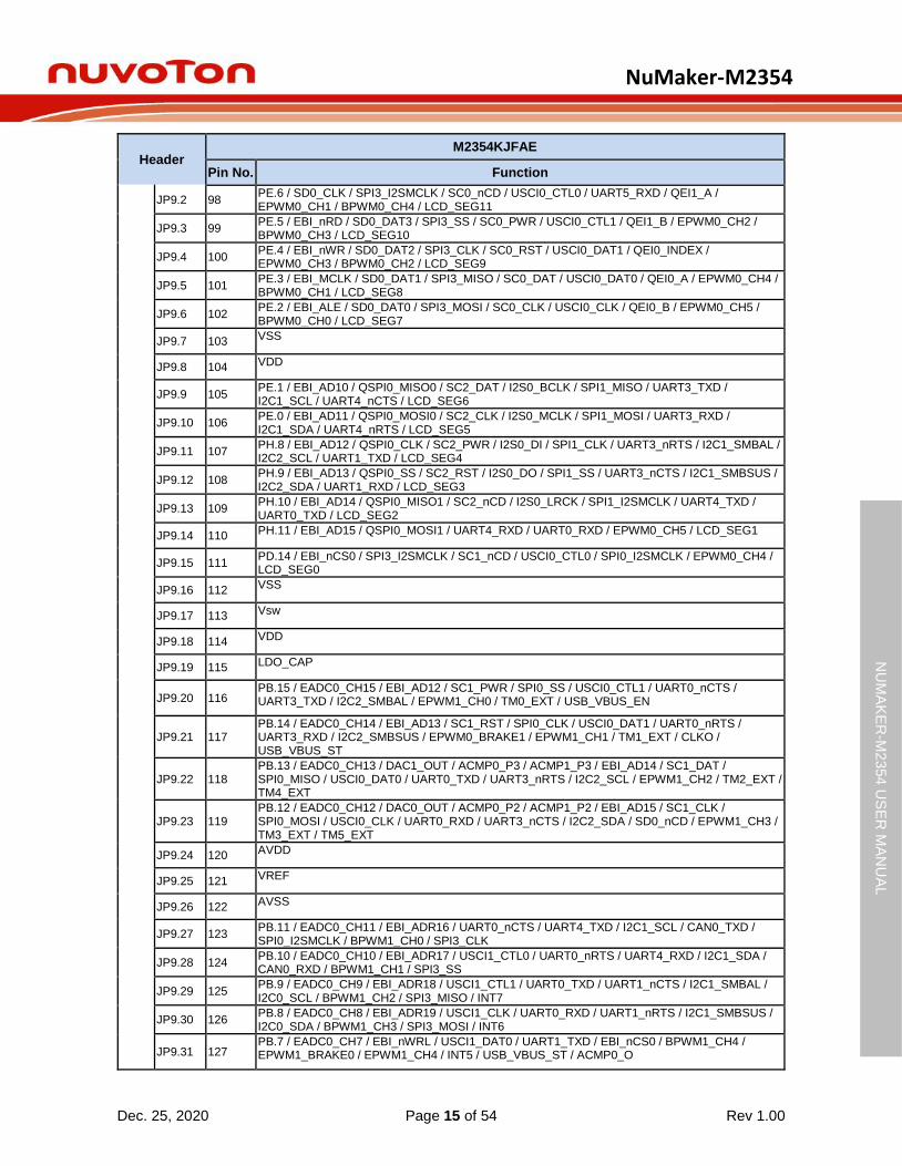
Header M2354KJFAE
Pin No. Function
JP9.2 98 PE.6 / SD0_CLK / SPI3_I2SMCLK / SC0_nCD / USCI0_CTL0 / UART5_RXD / QEI1_A / EPWM0_CH1 / BPWM0_CH4 / LCD_SEG11
JP9.3 99 PE.5 / EBI_nRD / SD0_DAT3 / SPI3_SS / SC0_PWR / USCI0_CTL1 / QEI1_B / EPWM0_CH2 / BPWM0_CH3 / LCD_SEG10
JP9.4 100 PE.4 / EBI_nWR / SD0_DAT2 / SPI3_CLK / SC0_RST / USCI0_DAT1 / QEI0_INDEX / EPWM0_CH3 / BPWM0_CH2 / LCD_SEG9
JP9.5 101 PE.3 / EBI_MCLK / SD0_DAT1 / SPI3_MISO / SC0_DAT / USCI0_DAT0 / QEI0_A / EPWM0_CH4 / BPWM0_CH1 / LCD_SEG8
JP9.6 102 PE.2 / EBI_ALE / SD0_DAT0 / SPI3_MOSI / SC0_CLK / USCI0_CLK / QEI0_B / EPWM0_CH5 / BPWM0_CH0 / LCD_SEG7
JP9.7 103 VSS
JP9.8 104 VDD
JP9.9 105 PE.1 / EBI_AD10 / QSPI0_MISO0 / SC2_DAT / I2S0_BCLK / SPI1_MISO / UART3_TXD / I2C1_SCL / UART4_nCTS / LCD_SEG6
JP9.10 106 PE.0 / EBI_AD11 / QSPI0_MOSI0 / SC2_CLK / I2S0_MCLK / SPI1_MOSI / UART3_RXD / I2C1_SDA / UART4_nRTS / LCD_SEG5
JP9.11 107 PH.8 / EBI_AD12 / QSPI0_CLK / SC2_PWR / I2S0_DI / SPI1_CLK / UART3_nRTS / I2C1_SMBAL / I2C2_SCL / UART1_TXD / LCD_SEG4
JP9.12 108 PH.9 / EBI_AD13 / QSPI0_SS / SC2_RST / I2S0_DO / SPI1_SS / UART3_nCTS / I2C1_SMBSUS / I2C2_SDA / UART1_RXD / LCD_SEG3
JP9.13 109 PH.10 / EBI_AD14 / QSPI0_MISO1 / SC2_nCD / I2S0_LRCK / SPI1_I2SMCLK / UART4_TXD / UART0_TXD / LCD_SEG2
JP9.14 110 PH.11 / EBI_AD15 / QSPI0_MOSI1 / UART4_RXD / UART0_RXD / EPWM0_CH5 / LCD_SEG1
JP9.15 111 PD.14 / EBI_nCS0 / SPI3_I2SMCLK / SC1_nCD / USCI0_CTL0 / SPI0_I2SMCLK / EPWM0_CH4 / LCD_SEG0
JP9.16 112 VSS
JP9.17 113 Vsw
JP9.18 114 VDD
JP9.19 115 LDO_CAP
JP9.20 116 PB.15 / EADC0_CH15 / EBI_AD12 / SC1_PWR / SPI0_SS / USCI0_CTL1 / UART0_nCTS / UART3_TXD / I2C2_SMBAL / EPWM1_CH0 / TM0_EXT / USB_VBUS_EN
JP9.21 117 PB.14 / EADC0_CH14 / EBI_AD13 / SC1_RST / SPI0_CLK / USCI0_DAT1 / UART0_nRTS / UART3_RXD / I2C2_SMBSUS / EPWM0_BRAKE1 / EPWM1_CH1 / TM1_EXT / CLKO / USB_VBUS_ST
JP9.22 118 PB.13 / EADC0_CH13 / DAC1_OUT / ACMP0_P3 / ACMP1_P3 / EBI_AD14 / SC1_DAT / SPI0_MISO / USCI0_DAT0 / UART0_TXD / UART3_nRTS / I2C2_SCL / EPWM1_CH2 / TM2_EXT / TM4_EXT
JP9.23 119 PB.12 / EADC0_CH12 / DAC0_OUT / ACMP0_P2 / ACMP1_P2 / EBI_AD15 / SC1_CLK / SPI0_MOSI / USCI0_CLK / UART0_RXD / UART3_nCTS / I2C2_SDA / SD0_nCD / EPWM1_CH3 / TM3_EXT / TM5_EXT
JP9.24 120 AVDD
JP9.25 121 VREF
JP9.26 122 AVSS
JP9.27 123 PB.11 / EADC0_CH11 / EBI_ADR16 / UART0_nCTS / UART4_TXD / I2C1_SCL / CAN0_TXD / SPI0_I2SMCLK / BPWM1_CH0 / SPI3_CLK
JP9.28 124 PB.10 / EADC0_CH10 / EBI_ADR17 / USCI1_CTL0 / UART0_nRTS / UART4_RXD / I2C1_SDA / CAN0_RXD / BPWM1_CH1 / SPI3_SS
JP9.29 125 PB.9 / EADC0_CH9 / EBI_ADR18 / USCI1_CTL1 / UART0_TXD / UART1_nCTS / I2C1_SMBAL / I2C0_SCL / BPWM1_CH2 / SPI3_MISO / INT7
JP9.30 126 PB.8 / EADC0_CH8 / EBI_ADR19 / USCI1_CLK / UART0_RXD / UART1_nRTS / I2C1_SMBSUS / I2C0_SDA / BPWM1_CH3 / SPI3_MOSI / INT6
JP9.31 127 PB.7 / EADC0_CH7 / EBI_nWRL / USCI1_DAT0 / UART1_TXD / EBI_nCS0 / BPWM1_CH4 / EPWM1_BRAKE0 / EPWM1_CH4 / INT5 / USB_VBUS_ST / ACMP0_O
NuMaker-M2354
Dec. 25, 2020 Page 16 of 54 Rev 1.00
NU
MA
KE
R-M
2354 U
SE
R M
AN
UA
L
Maker N
u-m
bed
NU
C472 U
ser M
an
ual
Header M2354KJFAE
Pin No. Function
JP9.32 128 PB.6 / EADC0_CH6 / EBI_nWRH / USCI1_DAT1 / UART1_RXD / EBI_nCS1 / BPWM1_CH5 / EPWM1_BRAKE1 / EPWM1_CH5 / INT4 / USB_VBUS_EN / ACMP1_O
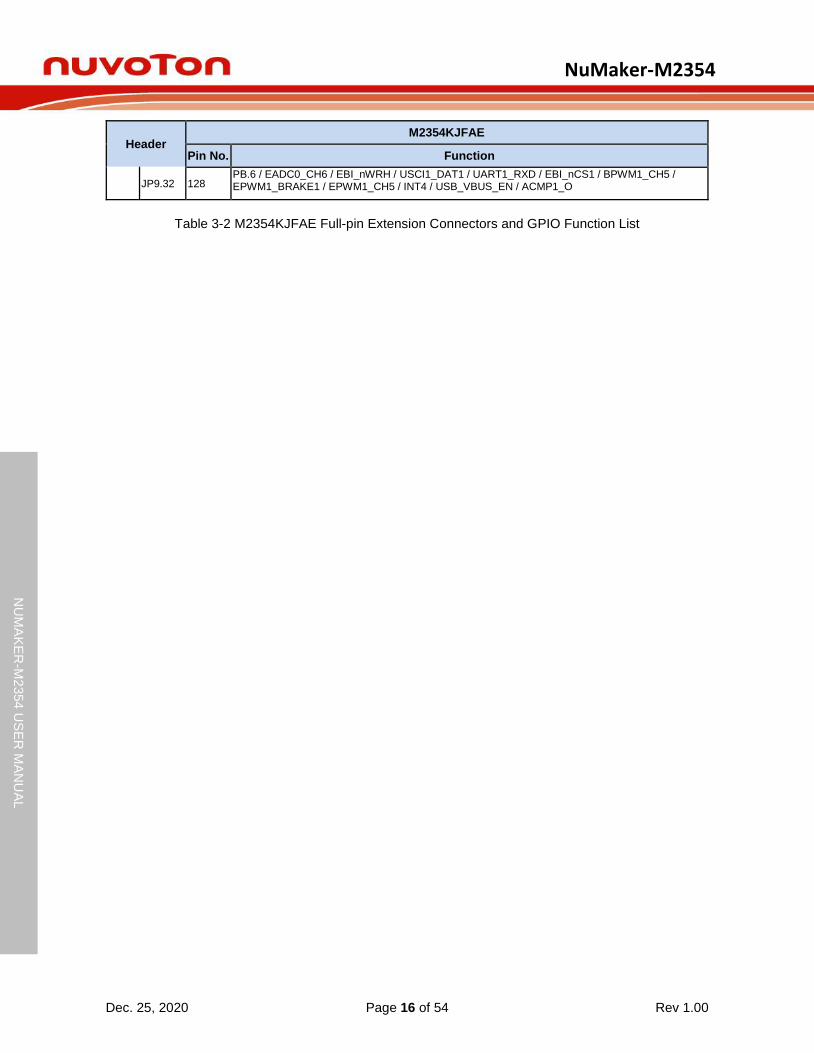
Table 3-2 M2354KJFAE Full-pin Extension Connectors and GPIO Function List

NuMaker-M2354
Dec. 25, 2020 Page 17 of 54 Rev 1.00
NU
MA
KE
R-M
2354 U
SE
R M
AN
UA
L
Maker N
u-m
bed
NU
C472 U
ser M
an
ual
3.3.2 Arduino UNO Compatible Extension Connectors
Figure 3-4 shows the Arduino UNO compatible extension connectors.
MISO CLK RESET SS
PE.1 PH.8 nRESET PH.9
VCC MOSI GND -
PE.0 VSS PH.10
EPWM1_CH3 PC.9 D8EPWM1_CH2 PC.10 D9
SPI0_SS EPWM0_CH2 PA.3 D10SPI0_MOSI EPWM0_CH5 PA.0 D11SPI0_MISO EPWM0_CH4 PA.1 D12
SPI0_CLK EPWM0_CH3 PA.2 D13
VSS VSS
VREF VREF
I2C1_SDA PG.3 SDA
I2C1_SCL PG.2 SCL
UART1_RXD BPWM0_CH3 PA.8 D0UART1_TXD BPWM0_CH2 PA.9 D1I2C0_SCL EPWM1_CH4 PC.1 D2I2C0_SDA EPWM1_CH5 PC.0 D3
EPWM0_CH0 PE.7 D4EPWM0_CH1 PE.6 D5EPWM1_CH0 PC.12 D6EPWM1_CH1 PC.11 D7
VINVSSVSS5V3VRSTIOREF VDD
NC
A5 PB.6 ADC0_CH6A4 PB.7 ADC0_CH7A3 PB.8 ADC0_CH8A2 PB.9 ADC0_CH9A1 PB.10 ADC0_CH10A0 PB.11 ADC0_CH11
Figure 3-4 Arduino UNO Compatible Extension Connectors

NuMaker-M2354
Dec. 25, 2020 Page 18 of 54 Rev 1.00
NU
MA
KE
R-M
2354 U
SE
R M
AN
UA
L
Maker N
u-m
bed
NU
C472 U
ser M
an
ual
Header
NuMaker-M2354
Header
NuMaker-M2354
Compatible to Arduino UNO
GPIO Pin of M2354 Compatible to Arduino UNO
GPIO Pin of M2354
NU4
NU4.1 D0 PA.8
NU2
NU2.6 A5 PB.6
NU4.2 D1 PA.9 NU2.5 A4 PB.7
NU4.3 D2 PC.1 NU2.4 A3 PB.8
NU4.4 D3 PC.0 NU2.3 A2 PB.9
NU4.5 D4 PE.7 NU2.2 A1 PB.10
NU4.6 D5 PE.6 NU2.1 A0 PB.11
NU4.7 D6 PC.12
NU1
NU1.8 VIN
-
NU4.8 D7 PC.11 NU1.7 VSS
NU3
NU3.1 D8 PC.9 NU1.6 VSS
NU3.2 D9 PC10 NU1.5 5V
NU3.3 D10 PA.3 NU1.4 3V
NU3.4 D11 PA.0 NU1.3 RST nRESET
NU3.5 D12 PA.1 NU1.2 IOREF VDD
NU3.6 D13 PA.2 NU1.1 NC -
NU3.7 AVSS GND
NU3.8 VREF VREF
NU3.9 SDA PG.3
NU3.10 SCL PG.2
Table 3-3 Arduino UNO Extension Connectors and M2354KJFAE Mapping GPIO List
NuMaker-M2354
Dec. 25, 2020 Page 19 of 54 Rev 1.00
NU
MA
KE
R-M
2354 U
SE
R M
AN
UA
L
Maker N
u-m
bed
NU
C472 U
ser M
an
ual
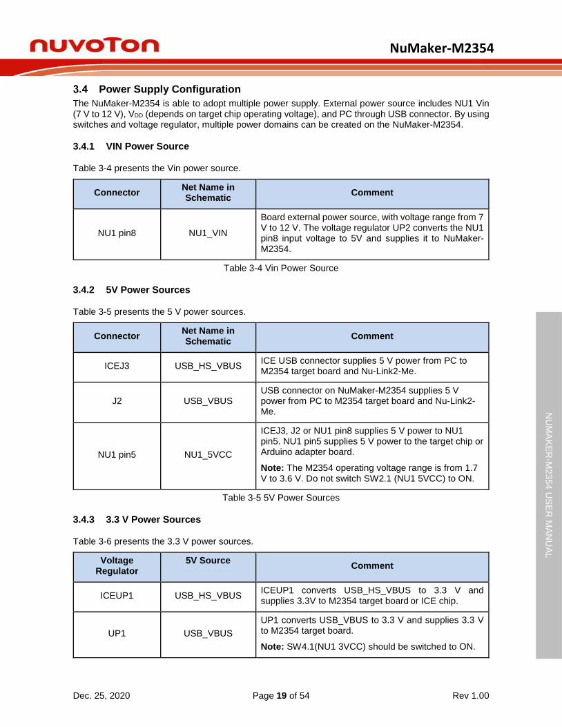
Power Supply Configuration
The NuMaker-M2354 is able to adopt multiple power supply. External power source includes NU1 Vin (7 V to 12 V), VDD (depends on target chip operating voltage), and PC through USB connector. By using switches and voltage regulator, multiple power domains can be created on the NuMaker-M2354.
3.4.1 VIN Power Source
Table 3-4 presents the Vin power source.
Connector Net Name in Schematic
Comment
NU1 pin8 NU1_VIN
Board external power source, with voltage range from 7 V to 12 V. The voltage regulator UP2 converts the NU1 pin8 input voltage to 5V and supplies it to NuMaker-M2354.
Table 3-4 Vin Power Source
3.4.2 5V Power Sources
Table 3-5 presents the 5 V power sources.
Connector Net Name in Schematic
Comment
ICEJ3 USB_HS_VBUS ICE USB connector supplies 5 V power from PC to M2354 target board and Nu-Link2-Me.
J2 USB_VBUS USB connector on NuMaker-M2354 supplies 5 V power from PC to M2354 target board and Nu-Link2-Me.
NU1 pin5 NU1_5VCC
ICEJ3, J2 or NU1 pin8 supplies 5 V power to NU1 pin5. NU1 pin5 supplies 5 V power to the target chip or Arduino adapter board.
Note: The M2354 operating voltage range is from 1.7 V to 3.6 V. Do not switch SW2.1 (NU1 5VCC) to ON.
Table 3-5 5V Power Sources
3.4.3 3.3 V Power Sources
Table 3-6 presents the 3.3 V power sources.
Voltage Regulator
5V Source Comment
ICEUP1 USB_HS_VBUS ICEUP1 converts USB_HS_VBUS to 3.3 V and supplies 3.3V to M2354 target board or ICE chip.
UP1 USB_VBUS
UP1 converts USB_VBUS to 3.3 V and supplies 3.3 V to M2354 target board.
Note: SW4.1(NU1 3VCC) should be switched to ON.
NuMaker-M2354
Dec. 25, 2020 Page 20 of 54 Rev 1.00
NU
MA
KE
R-M
2354 U
SE
R M
AN
UA
L
Maker N
u-m
bed
NU
C472 U
ser M
an
ual
UP1 NU1_5VCC
UP1 converts NU1_5VCC to 3.3 V and supplies 3.3 V to M2354 target board.
Note: SW4.1(NU1 3VCC) should be switched to ON.
Table 3-6 3.3 V Power Sources
3.4.4 1.8V Power Sources
Table 3-7 presents the 1.8 V power source.
Voltage Regular 5V Source Comment
ICEUP2 USB_HS_VBUS ICEUP2 converts USB_HS_VBUS to 1.8V and supplies 1.8V to M2354 target board or ICE chip.
UP3 NU1_5VCC UP3 converts NU1_5VCC to 1.8V and supplies 1.8V to internal VDDIO pin.
Table 3-7 1.8V Power Sources
3.4.5 Power Connectors
Table 3-8 presents the power connectors.
Connector Comment
JP13,JP14,JP15 VDD connector on the NuMaker-M2354.
Note: M2354 operating voltage range is from 1.7 V to 3.6 V.
JP4, JP5, JP10 and JP11,JP12
VSS connector on the NuMaker-M2354.
JPR_VBAT VBAT connector on the NuMaker-M2354.
Table 3-8 Power Connectors
3.4.6 USB Connectors
Table 3-9 presents the USB connectors.
Connector Comment
ICEJ3 ICE USB connector on Nu-Link2-Me for power supply, debugging and programming from PC.
J2 USB FS connector on NuMaker-M2354 for power supply.
Table 3-9 USB Connectors
3.4.7 Power Switches
Table 3-10 presents the power switches.
Switch Comment

NuMaker-M2354
Dec. 25, 2020 Page 21 of 54 Rev 1.00
NU
MA
KE
R-M
2354 U
SE
R M
AN
UA
L
Maker N
u-m
bed
NU
C472 U
ser M
an
ual
ICEJPR1
Configures the target chip operating voltage at 1.8 V / 3.3 V / 5 V.
Note: M2354 operating voltage range is from 1.7 V to 3.6 V. Do not switch ICEJPR1 (MCUVCC) to 5 V.
ICEJPR2 Configures the ICE chip operating voltage at 1.8 V / 3.3 V.
SW4_PowerSelect Configures the target chip power source from ICE or NU1_3VCC.
Table 3-10 Power Switches
3.4.8 Power Supply Models
External Power Supply through Nu-Link2-Me to Target Chip
The external power supply source on Nu-Link2-Me is shown in Figure 3-5.
ICE USB Connector (ICEJ3)
Nu-Link2-Me
Figure 3-5 External Power Supply Sources on Nu-Link2-Me
To use ICEJ3 as external power supply source with Nu-Link2-Me, please follow the steps below:
1. Solder the resistor on ICEJPR1 (MCUVCC) depends on the target chip operating voltage.
2. Solder the resistor on ICEJPR2 (ICEVCC) depends on the ICE chip operating voltage.
3. Connect the external power supply to ICEJ3.
Table 3-11 presents all power models when supplying external power through Nu-Link2-Me. The Nu-Link2-Me external power sources are highlighted in yellow.
Model Target Chip
Voltage ICEJ3
ICEJPR1 (MCUVCC) Selection [1]
ICEJPR2 (ICEVCC)
Selection [2]
ICE Chip
Voltage
SW4 Selection
J2 Vin JP13
1 1.8 V Connect
to PC 1.8 V 1.8 V 1.8 V Off - -
1.8 V output
2 3.3 V Connect
to PC 3.3 V (default)
3.3 V (default)
3.3 V Off - - 3.3 V output
3 5 V Connect
to PC 5V
3.3 V (default)
3.3 V Off - - 5 V
output
-: Unused.
Note:

NuMaker-M2354
Dec. 25, 2020 Page 22 of 54 Rev 1.00
NU
MA
KE
R-M
2354 U
SE
R M
AN
UA
L
Maker N
u-m
bed
NU
C472 U
ser M
an
ual
1. 0 Ω should be soldered between ICEJPR1’s MCUVCC and 1.8 V / 3.3 V / 5 V.
2. 0 Ω should be soldered between ICEJPR2’s ICEVCC and 1.8 V / 3.3 V.
Table 3-11 Supply External Power through Nu-Link2-Me
External Power Supply through M2354 target board to Target Chip
The external power supply sources on M2354 target board are shown in Figure 3-6.
Figure 3-6 External Power Supply Sources on M2354 target board
To use Vin or J2 as external power supply source, please follow the steps below:
1. Switch the SW4.2 to ON.
2. Remove the resistor on ICEJPR1 (MCUVCC).
3. Solder the resistor on ICEJPR2 (ICEVCC) depends on the ICE chip operating voltage.
4. Connect the external power supply to Vin or J2.
To use JP13/JP14/JP15 as external power supply source, please follow the steps below:
1. Switch the SW4 to OFF.
2. Remove the resistor on ICEJPR1 (MCUVCC).
3. Solder the resistor on ICEJPR2 (ICEVCC) depends on the ICE chip operating voltage.
4. Connect ICEJ3 to PC.
5. Connect the external power supply to JP13.
To use Vin or J2 as external power supply source with Nu-Link2-Me separated from NuMaker-M2354, please follow the steps below:
1. Switch the SW4.2 to ON.
2. Separate the Nu-Link2-Me from NuMaker-M2354.
3. Connect the external power supply to Vin or J2.

NuMaker-M2354
Dec. 25, 2020 Page 23 of 54 Rev 1.00
NU
MA
KE
R-M
2354 U
SE
R M
AN
UA
L
Maker N
u-m
bed
NU
C472 U
ser M
an
ual
To use JP13/JP14/JP15 as external power supply source with Nu-Link2-Me separated from NuMaker-M2354, please follow the steps below:
1. Switch the SW4 to OFF.
2. Separate the Nu-Link2-Me from NuMaker-M2354.
3. Connect the external power supply to JP13.
Figure 3-7 Separate the Nu-Link2-Me from NuMaker-M2354
Table 3-12 presents all power models when supplying external power through the M2354 target board. The M2354 target board external power sources are highlighted in yellow.
Model Target Chip
Voltage Vin [1] J2 ICEJ3
SW4 Selection
JP13 ICEJPR1
(MCUVCC) Selection [2]
ICEJPR2 (ICEVCC)
Selection [3]
ICE Chip Voltage [4]
4 3.3 V 7 V ~ 12 V
Input - -
SW4.2 ON
3.3 V output Remove resistor
3.3 V 3.3 V
5 3.3 V - Connect
to PC -
SW4.2 ON
3.3 V output Remove resistor
3.3 V 3.3 V
6 1.8 V ~ 3.6 V - [5] - [5] Connect to
PC OFF DC Input
1.8 V ~ 3.6 V Remove resistor
1.8 V / 3.3 V 1.8 V / 3.3 V
7 1.8 V ~ 3.6 V - [5] - [5] Nu-Link2-Me
removed OFF DC Input
1.8 V ~ 3.6 V - - -
-: Unused.
Note:
1. The Vin input voltage will be converted by voltage regulator UP2 to 5 V.
2. 0Ω should be removed from ICEJPR1’s MCUVCC and 1.8 V / 3.3 V / 5 V.
3. 0Ω should be soldered between ICEJPR2’s ICEVCC and 1.8 V / 3.3 V.
4. The ICE chip voltage should be close to the target chip voltage.
5. JP13 external power input only provides voltage to the target chip. Supplying external power to Vin or J2 can provide 5V to NU1 pin5 (5V) and 3.3V to NU1 pin4 (3VCC).
Table 3-12 Supply External Power for M2354 target board

NuMaker-M2354
Dec. 25, 2020 Page 24 of 54 Rev 1.00
NU
MA
KE
R-M
2354 U
SE
R M
AN
UA
L
Maker N
u-m
bed
NU
C472 U
ser M
an
ual
External Reference Voltage Connector
Table 3-14 presents the external reference voltage connector.
Connector Comment
VREF1 VREF1 is used to easily connect to the external reference voltage pin of the target chip. Remove the L11 ferrite bead before using it.
Table 3-13 External Reference Voltage Connector
Ammeter Connector
Table 3-14 presents the ammeter connector.
Connector Comment
AMMETER AMMETER is used to easily measure the target chip power consumption. Remove the R16 resistor before using it.
Table 3-14 Ammeter Connector
Remove the R16 Resistor
Figure 3-8 Wiring between Ammeter Connector and Ammeter
Push-Buttons
Table 3-15 presents the push-buttons.
Component Comment
ICESW1 Off-line program button to start off-line programming the target chip.
SW1 Reset button to reset the target chip.
SW2 Push-Button to control application process.
Table 3-15 Push-Buttons
MicroSD Card Slot
U9: MicroSD card slot for application use.

NuMaker-M2354
Dec. 25, 2020 Page 25 of 54 Rev 1.00
NU
MA
KE
R-M
2354 U
SE
R M
AN
UA
L
Maker N
u-m
bed
NU
C472 U
ser M
an
ual
SWD / ETM interface
The ETM is a debug interface that enables reconstruction of program execution. It provides instruction and data tracing of a processor. The traced data can be used to capture events leading to a breakpoint, or used for code coverage statistics or execution information.
ETM1: SWD / ETM interface connector with 20 pins on the NuMakerM2354 board.
LEDs
Table 3-16 presents the LEDs.
Component Comment
Power LED The power LED indicates that the NuMaker-M2354 is powered.
PD2, PD3 LED The LED is connected to the target chip PD.2 and PD.3.
ICES0, ICES1, ICES2 and ICES3
Nu-Link2-Me status LED.
Table 3-16 LEDs
Wi-Fi Module (ESP-12)
U10: Wi-Fi Module ESP-12 on the NuMaker-M2354 board for application use.
NuMaker-M2354
ESP-12 Description
UART4_RXD UTXD_ESP12 UART data out from ESP-12
UART4_TXD URXD_ESP12 UART data in from ESP-12
UART4_nRTS UCTS_ESP12 CTS pin for flow control
UART4_nCTS URTS_ESP12 RTS pin for flow control
PD.12 IO0_ESP12 General Purpose Input/Output Interface
PC.13 RST_ESP12 General Purpose Input/Output Interface
J5 IO0_ESP12 For Wi-Fi updated
Table 3-17 Optional Function of ESP-12

NuMaker-M2354
Dec. 25, 2020 Page 26 of 54 Rev 1.00
NU
MA
KE
R-M
2354 U
SE
R M
AN
UA
L
Maker N
u-m
bed
NU
C472 U
ser M
an
ual
HTN-LCD Panel
The NuMaker-M2354 equip with a COM/SEG LCD interface which can connect to LCD panel.
JLCD_1: 8 COM / 40 SEG LCD connective interface.
JLCD_2: LCD Panel (HTN-3.3V)
Figure 3-9 LCD interface

NuMaker-M2354
Dec. 25, 2020 Page 27 of 54 Rev 1.00
NU
MA
KE
R-M
2354 U
SE
R M
AN
UA
L
Maker N
u-m
bed
NU
C472 U
ser M
an
ual
Nu-Link2-Me
The Nu-Link2-Me is an attached on-board debugger and programmer. The Nu-Link2-Me supports on-chip debugging, online and off-line ICP programming through SWD interface. The Nu-Link2-Me also supports virtual COM port (VCOM) for printing debug messages on PC. Besides, the programming status can be shown on the built-in LEDs. Lastly, the Nu-Link2-Me can be detached from the evaluation board and becoming a stand-alone mass production programmer. For more information about Nu-Link2-Me, please refer to Nu-Link2-Pro Debugger and Programmer User Manual.
3.13.1 VCOM Switches
Table 3-18 presents how to set the VCOM function by ICESW2.
ICESW2
Pin Function Description
1 TXD On: Connect target chip PA.7 (UART0_TXD) to Nu-Link2-Me.
Off: Disconnect target chip PA.7 (UART0_TXD) to Nu-Link2-Me.
2 RXD On: Connect target chip PA.6 (UART0_RXD) to Nu-Link2-Me.
Off: Disconnect target chip PA.6 (UART0_RXD) to Nu-Link2-Me.
Note: Pin 3 and 4 is unused.
Table 3-18 VCOM Function of Nu-Link2-Me
3.13.2 Status LEDs
Table 3-19 presents the status LEDs patterns for different operation on Nu-Link2-Me.
Operation Status Status LED
ICES0 ICES1 ICES2 ICES3
Power on Flash x 3 Flash x 3 Flash x 3 Flash x 3
Connected to IDE/NuTool Flash x 3 Flash x 3 Flash x 3 On
ICE online (Not connected to a target chip) On - Flash x 3 Flash x 3
ICE online (Connected to a target chip) On - - On
ICE online (Failed to connect to a target chip) On Any Flash On
During Off-line Programming - On - Flash
Off-line Programming Completed On - - -
Off-line Programming Completed (Auto mode) On On - -
Off-line Programming Failed On Flash - -
Table 3-19 Status LEDs patterns of Nu-Link2-Me

NuMaker-M2354
Dec. 25, 2020 Page 28 of 54 Rev 1.00
NU
MA
KE
R-M
2354 U
SE
R M
AN
UA
L
Maker N
u-m
bed
NU
C472 U
ser M
an
ual
4 QUICK START
Toolchains Support
Install the preferred toolchain. Please make sure at least one of the toolchains has been installed.
KEIL MDK Nuvoton edition M0/M23
IAR EWARM
NuEclipse (GCC)(Windows)
NuEclipse (GCC)(Linux)
Nuvoton Nu-Link Driver Installation
Download and install the latest Nuvoton Nu-Link Driver.
Download and install Nu-Link_Keil_Driver when using Keil MDK.
Download and install Nu-Link_IAR_Driver when using IAR EWARM.
Skip this step when using NuEclipse.
Please install the Nu-Link USB Driver as well at the end of the installation. The installation is presented in Figure 4-1 and Figure 4-2.
Figure 4-1 Nu-Link USB Driver Installation Setup

NuMaker-M2354
Dec. 25, 2020 Page 29 of 54 Rev 1.00
NU
MA
KE
R-M
2354 U
SE
R M
AN
UA
L
Maker N
u-m
bed
NU
C472 U
ser M
an
ual
Figure 4-2 Nu-Link USB Driver Installation
NuMaker-M2354
Dec. 25, 2020 Page 30 of 54 Rev 1.00
NU
MA
KE
R-M
2354 U
SE
R M
AN
UA
L
Maker N
u-m
bed
NU
C472 U
ser M
an
ual
BSP Firmware Download
Download and unzip the Board Support Package (BSP).
Hardware Setup
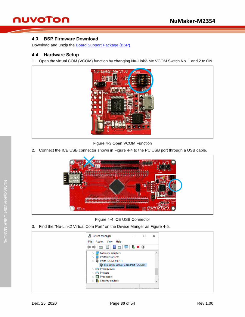
1. Open the virtual COM (VCOM) function by changing Nu-Link2-Me VCOM Switch No. 1 and 2 to ON.
Figure 4-3 Open VCOM Function
2. Connect the ICE USB connector shown in Figure 4-4 to the PC USB port through a USB cable.
Figure 4-4 ICE USB Connector
3. Find the “Nu-Link2 Virtual Com Port” on the Device Manger as Figure 4-5.
NuMaker-M2354
Dec. 25, 2020 Page 31 of 54 Rev 1.00
NU
MA
KE
R-M
2354 U
SE
R M
AN
UA
L
Maker N
u-m
bed
NU
C472 U
ser M
an
ual
Figure 4-5 Device Manger
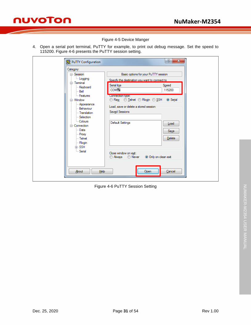
4. Open a serial port terminal, PuTTY for example, to print out debug message. Set the speed to 115200. Figure 4-6 presents the PuTTY session setting.
Figure 4-6 PuTTY Session Setting

NuMaker-M2354
Dec. 25, 2020 Page 32 of 54 Rev 1.00
NU
MA
KE
R-M
2354 U
SE
R M
AN
UA
L
Maker N
u-m
bed
NU
C472 U
ser M
an
ual
Finding the Example Project
Use the “Blinky” project as an example. The project can be found under the BSP folder as shown in
Figure 4-7.
M2354_BSP
SampleCode
NuMaker
Blinky
Keil
IAR
GCC
Figure 4-7 Blinky Project Folder Path
Executing the Project under Toolchains
Open and execute the project under the toolchain. The section 4.6.1, 4.6.2, and 4.6.3 describe the steps of executing project in Keil MDK, IAR EWARM and NuEclipse, respectively.
4.6.1 Keil MDK
This section provides steps to beginners on how to run a project by using Keil MDK.
1. Double click the “Blinky.uvprojx” to open the project.
2. Make sure the debugger is “Nuvoton Nu-Link Debugger” as shown in Figure 4-8 and Figure 4-9.
Note: If the dropdown menu in Figure 4-8 does not contain “Nuvoton Nu-Link Debugger” item, please rework section 4.2.
2
1
Figure 4-8 Debugger Setting in Options Window

NuMaker-M2354
Dec. 25, 2020 Page 33 of 54 Rev 1.00
NU
MA
KE
R-M
2354 U
SE
R M
AN
UA
L
Maker N
u-m
bed
NU
C472 U
ser M
an
ual
3
4
5
Figure 4-9 Programming Setting in Options Window
3. Rebuild all target files. After successfully compiling the project, download code to the Flash memory. Click “Start/Stop Debug Section” icon to enter debug mode.
Figure 4-10 Compile and Download the Project

NuMaker-M2354
Dec. 25, 2020 Page 34 of 54 Rev 1.00
NU
MA
KE
R-M
2354 U
SE
R M
AN
UA
L
Maker N
u-m
bed
NU
C472 U
ser M
an
ual
4. Figure 4-11 shows the debug mode under Keil MDK. Click “Run” and the debug message will be printed out as shown in Figure 4-12. User can debug the project under debug mode by checking source code, assembly language, peripherals’ registers, and setting breakpoint, step run, value monitor, etc.
Figure 4-11 Keil MDK Debug Mode
Figure 4-12 Debug Message on Serial Port Terminal Windows

NuMaker-M2354
Dec. 25, 2020 Page 35 of 54 Rev 1.00
NU
MA
KE
R-M
2354 U
SE
R M
AN
UA
L
Maker N
u-m
bed
NU
C472 U
ser M
an
ual
4.6.2 IAR EWARM
This section provides steps to beginners on how to run a project by using IAR EWARM.
1. Double click the “Blinky.eww” to open the project.
2. Make sure the toolbar contain “Nu-Link” item as shown in Figure 4-13.
Note: If the toolbar does not contain “Nu-Link” item, please rework section 4.2.
Figure 4-13 IAR EWARM Window
3. Make target file as presented in Figure 4-14. After successfully compile the project, download code to the flash memory and enter debug mode.
1 3
2
1. Make2. Successfully compile3. Download and Debug
Figure 4-14 Compile and Download the Project

NuMaker-M2354
Dec. 25, 2020 Page 36 of 54 Rev 1.00
NU
MA
KE
R-M
2354 U
SE
R M
AN
UA
L
Maker N
u-m
bed
NU
C472 U
ser M
an
ual
4. Figure 4-15 shows the debug mode under IAR EWARN. Click “Go” and the debug message will be printed out as shown in Figure 4-16. The project can be debugged under debug mode by checking source code, assembly language, peripherals’ registers, and setting breakpoint, step run, value monitor, etc.
1 3
1. Go2. Break3. Reset
2
Figure 4-15 IAR EWARM Debug Mode
Figure 4-16 Debug Message on Serial Port Terminal Windows

NuMaker-M2354
Dec. 25, 2020 Page 37 of 54 Rev 1.00
NU
MA
KE
R-M
2354 U
SE
R M
AN
UA
L
Maker N
u-m
bed
NU
C472 U
ser M
an
ual
4.6.3 NuEclipse
This section provides steps to beginners on how to run a project by using NuEclipse. Please make sure the filenames and project folder path contain neither invalid character nor space.
1. Double-click NuEclipse.exe to open the toolchain.
2. Import the “Blinky” project by following the steps presented in Figure 4-17and Figure 4-18.
1
2
3
4
Figure 4-17 Import the Project in NuEclipse
5
6
7
Figure 4-18 Import Projects Windows
3. Click the “Blinky” project and find the project properties as shown in Figure 4-19. Make sure the
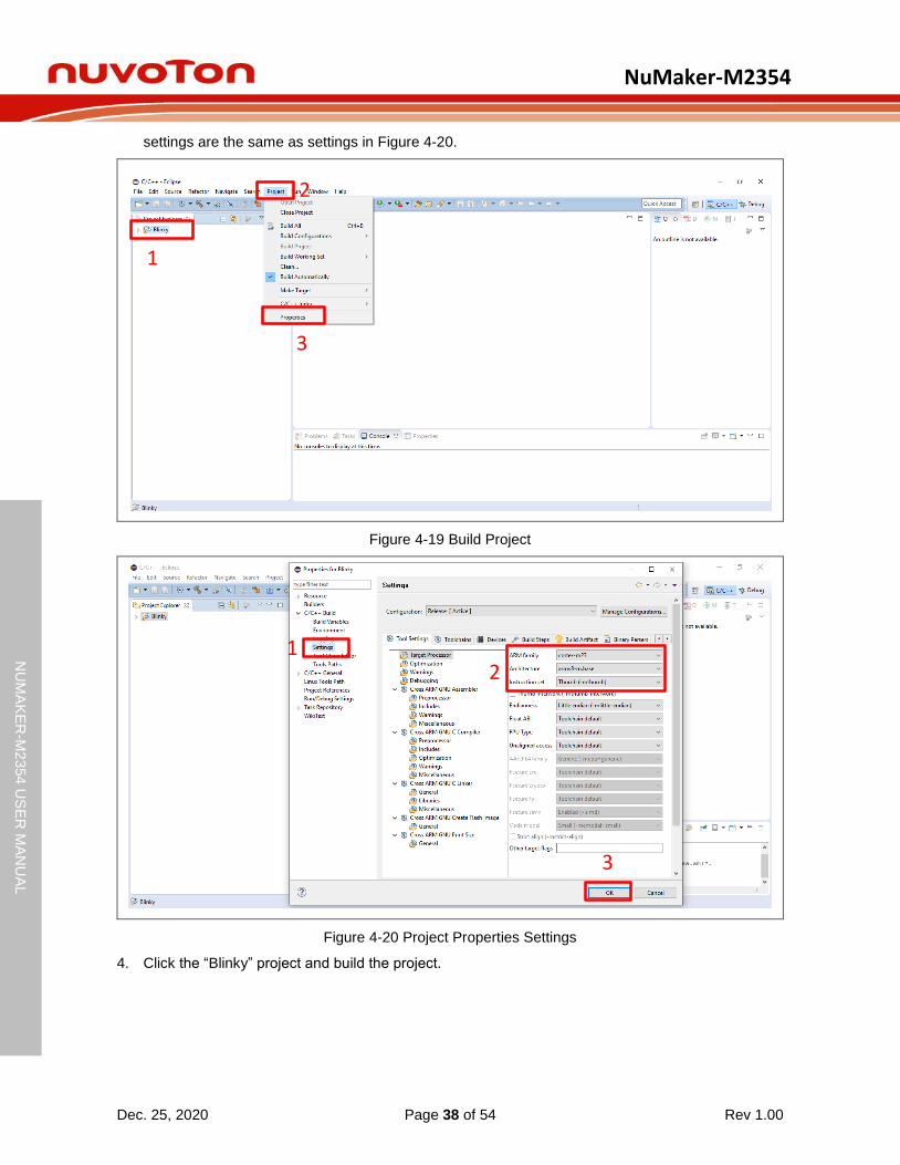
NuMaker-M2354
Dec. 25, 2020 Page 38 of 54 Rev 1.00
NU
MA
KE
R-M
2354 U
SE
R M
AN
UA
L
Maker N
u-m
bed
NU
C472 U
ser M
an
ual
settings are the same as settings in Figure 4-20.
1
2
3
Figure 4-19 Build Project
12
3
Figure 4-20 Project Properties Settings
4. Click the “Blinky” project and build the project.

NuMaker-M2354
Dec. 25, 2020 Page 39 of 54 Rev 1.00
NU
MA
KE
R-M
2354 U
SE
R M
AN
UA
L
Maker N
u-m
bed
NU
C472 U
ser M
an
ual
1
2
3
Figure 4-21 Build Project
5. After the project is built, click the “Blinky” project and set the “Debug Configuration” as shown in Figure 4-22. Follow the settings presented in Figure 4-23, Figure 4-24 and Figure 4-25 to enter debug mode.
1
2
3
Figure 4-22 Open Debug Configuration

NuMaker-M2354
Dec. 25, 2020 Page 40 of 54 Rev 1.00
NU
MA
KE
R-M
2354 U
SE
R M
AN
UA
L
Maker N
u-m
bed
NU
C472 U
ser M
an
ual
4[1]
5[2]
Note 1: Double click the “GDB Nuvoton Nu-Link Debugging” to create the subitem.
Note 2: After the project is built, the “*.elf” file will be shown in “C/C++ Application” frame.
Figure 4-23 Main Tab Configuration
6
7
Figure 4-24 Debugger Tab Configuration

NuMaker-M2354
Dec. 25, 2020 Page 41 of 54 Rev 1.00
NU
MA
KE
R-M
2354 U
SE
R M
AN
UA
L
Maker N
u-m
bed
NU
C472 U
ser M
an
ual
8
11
9[1]
10
Note 1: Please follow the settings highlighted in green triangles and configure other settings depending on the needs.
Figure 4-25 Startup Tab Configuration

NuMaker-M2354
Dec. 25, 2020 Page 42 of 54 Rev 1.00
NU
MA
KE
R-M
2354 U
SE
R M
AN
UA
L
Maker N
u-m
bed
NU
C472 U
ser M
an
ual
6. Figure 4-26 shows the debug mode under NuEclipse. Click “Resume” and the debug message will be printed out as shown in Figure 4-27. User can debug the project under debug mode by checking source code, assembly language, peripherals’ registers, and setting breakpoint, step run, value monitor, etc. For more information about how to use NuEclipse, please refer to the NuEclipse User Manual.
1 2 4 31. Resume2. Suspend3. Restart the debugging session4. Terminate
Figure 4-26 NuEclipse Debug Mode
Figure 4-27 Debug Message on Serial Port Terminal Windows

NuMaker-M2354
Dec. 25, 2020 Page 43 of 54 Rev 1.00
NU
MA
KE
R-M
2354 U
SE
R M
AN
UA
L
Maker N
u-m
bed
NU
C472 U
ser M
an
ual
5 NUMAKER-M2354 SCHEMATICS
Nu-Link2-Me
Figure 5-1 shows the Nu-Link2-Me circuit. The Nu-Link2-Me is a debugger and programmer that supports on-line programming and debugging through a SWD interface.
Figure 5-1 Nu-Link2-Me Circuit
GND
GREENRED
SW
DH
_C
LK
NU
LIN
K_
ID0
NU
LIN
K_
ID1
SW
DH
_D
AT
SW
DH
_R
ST
#IC
EV
DD
ICE
LE
D
ICEVDDICE_RST
HX
T_
I
HXT_O
SWO
KEY1ISPLED
US
B_
HS
_R
EX
T
US
B_
HS
_C
AP
US
B_
HS
_V
BU
S
ICEVDDGND
USB_HS_CAP
US
B_
HS
_D
-
US
B_
HS
_D
+G
ND
SP
IM_
CS
SP
IM_
MIS
O0
ICE
_C
LK
ICE
_D
AT
ICEVDD
GND
SP
IM_
CL
K
SP
IM_
MO
SI0
RESETDEBUG
ICE_RST
ICE_RSTICE_CLKICE_DAT
ICE_DAT
ICE_CLK
ETMCK_MOSIETMD0_MISO
ETMD3_SSETMD2_CK
ICE_RXICE_RX_S
VCOM SWITCH
ICE_TX_S ICE_TX
ETMD3_SSETMD2_CKETMD0_MISOETMCK_MOSI
NULINK_ID0
NULINK ID
Nu-Trace, ID0 = 1, ID1 = 1Nu-Link2, ID0 = 0, ID1 = 1Nu-LInk2-Me, ID0 = 0, ID1 = 0
NULINK_ID1
SWDH_DAT
SWDH_RST#SWDH_CLK
ICE_RX_SICE_TX_S
HS
US
B_
VD
D3
3
HXT_O
HXT_I
12M Crystal
Title
Size File Name : Rev
Date: Sheet of
Author :
Nu-Link2-Me 1.0
Nu-Link2-Me
CACHENA3
1 3Friday, May 22, 2020
SPIM_MISO0
SPI FLASH
ICEJ3
micro USB 5pin
MICRO_USB_AB
VBUS1
D-2
D+3
GND5
ID4
Shield6
Shield7
Shield8
Shield9
Shield10
Shield11
ICEX1
12MHz SMD X3225B1
XIN
2
GND
4GND
3XOUT
SPIM_CLK_LV
ICEC11 20p
C0603
SPIM_CS
SPIM_CS_LV
SPIM_MOSI0_LV
ICER210K
R0603
SPIM_MOSI0SPIM_CLKSPIM_CS_LV
ICEUP2ACE1117_ADJ
IN3
AD
J1
OU
T2
OU
T4
ICEL1
FERRITE BEAD
SPIM_MOSI0_LVSPIM_CLK_LV
ICEC10 20p
C0603
ICEUP1AMS1117_3.3v
IN3
GN
D1
OU
T2
OU
T4
ICEC6
1u
C0603
ICER70
ICEU2
W25Q16JVSSIQ
SOP8\5.23/1.27MM
CS#1
DO2
WP#3
GND4
DI5CLK6HOLD#7VCC8
1 2
ICES30805 LED G (綠光) 高亮
LED0805
ICEJPR2
1&2 (0 ohm)
123
ICER410K
R0603
1 2
ICED4
SS24A
ICEJPR1
1&2 (0 ohm)
1234
ICER1910KR0603
1 2
ICES00805 LED R (紅光) 高亮
LED0805
ICEC7
4.7u
C0603
ICER310KR0603
ICER1810KR0603
ICEJ4
HEADER 2.54 5X2 (NC)
1 23 45 67 89 10
ICER510KR0603
ICERP1
8P4R-330
8P4RA
1 23 45 67 8
ICECT210uF/10VTANT-A
12
1 2
ICES20805 LED R (紅光) 高亮LED0805
ICESW13x6x5 2PIN SMD
SW-2P-SMD
ICER1200 1%
R0603
ICESW2
SMD HPS604-E
1 2
ICES10805 LED Y (黃光)高亮
LED0805ICER982, 1%
R0603
ICEC5
0.1u
C0603
ICEC12
0.1u
C0603
ICEC8470p
C0603
ICER60
ICEU1
<M48SSIDAE>
PB
.61
PB
.52
PB
.43
PB
.34
PB
.25
PB
.16
PB
.07
PA
.11
8
PA
.10
9
PA
.910
PA
.811
PF
.612
VB
AT
13
PF
.514
PF
.415
PF
.316
PF.217PC.718PC.619PA.720PA.621VSS22VDD23LDO_CAP24PA.525PA.426PA.327PA.228PA.129PA.030VDDIO31nRESET32
PF
.033
PF
.134
PC
.535
PC
.436
PC
.337
PC
.238
PC
.139
PC
.040
HS
US
B_
VR
ES
41
HS
US
B_
VD
D3
342
HS
US
B_
VB
US
43
HS
US
B_
D-
44
HS
US
B_
VS
S45
HS
US
B_
D+
46
HS
US
B_
VD
D1
2_
CA
P47
HS
US
B_
ID48
VSS49
LDO_CAP50
VDD51
PC.1452
PB.1553
PB.1454
PB.1355
PB.1256
AVDD57
VREF58
AVSS59
PB.1160
PB.1061
PB.962
PB.863
PB.764
ICED30.1u
C0603
ICEL2
FERRITE BEAD
L0603
ICECT110uF/10VTANT-A
12
ICEC9
1uC0603
ICEC1
0.1u
C0603
ICEJ2
HEADER04(NC)
1234
ICEJ1
HEADER_5(NC)
12345
ICEC3
1u
C0603
ICE INTERFACE
ICEC2
1u
C0603
1 2ICED1
SS24A
SN74LV2T45DCUR
ICEU4
SOP8/3.1/0.5
GND4 A23
VCCA1
DIR5
A12
B26B17VCCB8
ICEC4
0.1u
C0603
SN74LV2T45DCUR
ICEU3
SOP8/3.1/0.5
GND4 A23
VCCA1
DIR5
A12
B26B17VCCB8
ICECT310uF/10V
12
ICER8120,1%R0603
3.3V
ICEVDD
ICE5V
ICEVCC
3.3VUSB_HS_VBUS
ICEVDDICEVCC
1.8V
MCUVCC
ICEVDD
MCUVCC
ICEVDD
ICEVDD
ICEVDD
USB_HS_VBUS
ICEVDD
MCUVCC_DIODE
MCUVCC_DIODE
USB_HS_VBUS
3.3V
ICE5V
USB_HS_VBUS
3.3V ICEVDD
3.3V
3.3V
3.3V ICEVDD
RESET
TICEDAT
GND
3.3V
TICECLK
M2354_TXDM2354_RXD
MCUVCC_DIODE
ICE5V
SWDH_CLKSWDH_DAT
SWDH_RST#
ICE_RX_S
SWO
ICE_TX_S
MSG_EN
MS
G_
EN
ETMD3_SS I2C1_SCL QSPI_SS BUSY
5V
ETMD0_MISO UART0_TX QSPI_MISOFAILICE_TX
ETMCK_MOSI UART0_RX QSPI_MOSIPASSICE_RX
ETMD2_CK I2C1_SDA QSPI_CLK START
DP
DM
USB_HS_D+
USB_HS_D-
USB 2.0 HIGH SPEED DEVICES
ICELED
RED
ISPLED
GREEN
DMDP
LED
KEY
KEY1
ICEVDD
5V
Power Switch
1.8V 3.3V3.3V 1.8V
Off-page Connector

NuMaker-M2354
Dec. 25, 2020 Page 44 of 54 Rev 1.00
NU
MA
KE
R-M
2354 U
SE
R M
AN
UA
L
Maker N
u-m
bed
NU
C472 U
ser M
an
ual
M2354 target Board
Figure 5-2 shows the pin assignment of the M2354.
Figure 5-2 M2354 Pin Assignment
R4330R
R0603
VCC
12
POWER
Red(LED0805)
LED
ICEDATICECLKRESETM2354_TXD
M2354_RXD
VCC
ICE
XT1_IN
C320pF
R1NC
C4
20pF
XT1_OUT
Y2
12MHz SMD X3225B
XIN1
GND2
GND4
XOUT3
CRYSTAL
P69P68P67P66P65
P72P71P70
P67 PD.9 COM7P66 PF.1 ICECLKP65 PF.0 ICEDAT
P72 PC.2 COM2P71 PC.3 COM3P70 PC.4 COM4P69 PC.5 COM5P68 PD.8 COM6
XT32_IN XT32_OUT
C2
20pF
Y3
X3215 32.768KHz SMDC1
20pF
~
~
P97
P128
P1
P32
~
P33
P64
~
P65
P96
P57 PA.3 D10 SPI0_SSD9 EPWM1_CH2PC.10P7D8 EPWM1_CH3PC.9P8
PA.1P59 D12 SPI0_MISOP60 PA.0 D11 SPI0_MOSI
P58
P60P57
P1
PA.2P58 D13 SPI0_CLK
P107
P105
P7P8
P59
JP1
HEADER 2.54 5X2 (NC)
1 23 45 67 89 10
P108
P106
PE.1P105 SPI1_MISOP106 PE.0 SPI1_MOSI
PF.10P25
P109
P2
P109 PH.10P108 PH.9 SPI1_SS
PH.8P107 SPI1_CLK
PF.6P29PF.7P28PF.8P27PF.9P26
GND
NU1_3VCCNU1_5VCCGNDGND
PF.4P32 XT32_OUTPF.5P31 XT32_IN
P30 VBAT
NU1_5VCCGND
P3
nRESET RESETP64VCC
VCC
NU1_3VCC
PC.11P6 EPWM1_CH1D7
P98
P6
P64
P5P4
PC.12P5 EPWM1_CH0D6PE.6P98 EPWM0_CH1D5
P74
P5
P6
PC.0P74 EPWM1_CH5D3P73
P97
NU1_VIN
PE.7P97 EPWM0_CH0D4
Digital In1
Digital In0
Analog In
NU1_VIN
PC.1P73 EPWM1_CH4D2
UNO Interface
PA.8 D0P16 UART1_RXDPA.9 D1P15 UART1_TXD
P122
P16P15
PB.6P128 A5 EADC0_CH6
P122 AVSS
P128
PB.8P126 A3 EADC0_CH8PB.7P127 A4 EADC0_CH7
P126P127
PG.2P21 SCL I2C1_SCLP22P21
P121 VREFP22 PG.3 SDAI2C1_SDA
P125
P121
PB.10P124 A1 EADC0_CH10PB.9P125 A2 EADC0_CH9
P124P123
PB.11P123 A0 EADC0_CH11
P24 PF.11P23 PG.4 SEG37P22 PG.3 SEG38P21 PG.2 SEG39
P24P23P22P21
P25
SW2
SMD按鍵開關6X6X5H(黑)卷代
SW4-SMD
R6210KR0603
VCC
P7
P24 PF.11
PE.8P41 TRACE_D3
PE.10P43 TRACE_D1PE.11P44 TRACE_D0PE.12P45 TRACE_CLK
PE.9P42 TRACE_D2UTXD_ESP12URXD_ESP12
VCCGND
VCC
URTS_ESP12UCTS_ESP12
P37
P18 PD.12IO0_ESP12
GND
P42P41P40P39P38
UART4_nRTSP46 PE.13
P17 PC.13RST_ESP12
P47P46P45P44P43
UART4_TXDP48 PC.7
UART4_nCTSP47 PC.8
WIFI Off-page
P53P52P51P50P49P48
UART4_RXDP49 PC.6
P58P57P56P55P54
P63P62P61P60P59
P64
P97 PE.7 SEG12
AVSSP122P122
12
LEDG
Yellow(LED0805)
R64330R
R0603
VCC
P89 PD.2
P109
P115
P112P113
P110P111
P121
P118P119
P116P117
P114
P124P125
P122P123
P120
P128
P126P127
Title
Size Document Number Rev
Date: Sheet of
NuMaker-M2354
V1.1M2354KJFAE(LQFP128) MCUCustom
2 10Tuesday , April 14, 2020
P74P73
P80P79P78P77P76P75
P85P84P83P82P81
P90P89P88P87P86
P96P95P94P93P92P91
P101P100
P99P98P97
P106P105P104P103P102
P108P107
12
LEDY
Green(LED0805)
SW1
SMD按鍵開關6X6X5H(黑)卷代
SW4-SMD
R65330R
R0603
VCC
P88 PD.3
R210KR0603
RESET
C5
1uFC0603
VCC
RESET
BUTTON
U1
M2354_LQFP128
PB
.51
PB
.42
PB
.33
PB
.24
PC
.12/U
AR
T0_T
XD
5
PC
.11/U
AR
T0_R
XD
6
PC
.10
7
PC
.98
PB
.19
PB
.010
VS
S11
VD
D12
PA
.11
13
PA
.10
14
PA
.915
PA
.816
PD
.12/C
LK
O18
PD
.11
19
PD
.10
20
X32_IN
/PF
.531
X32_O
UT
/PF
.432
XT1_IN/PF.337PF.2/XT1_OUT38
PE.841PE.942PE.1043PE.1144PE.1245PE.1346PC.847PC.748PC.649UART0_TXD/PA.750UART0_RXD/PA.651VSS52VDD53LDO_CAP54PA.555PA.456PA.357PA.258UART0_TXD/PA.159UART0_RXD/PA.060VDDIO61PE.1462PE.1563nRESET64
PF
.0/I
CE
_D
AT
65
PF
.1/I
CE
_C
LK
66
VS
S75
VD
D76
PD
.784
PD
.685
PD
.586
PD
.487
UA
RT
0_T
XD
/PD
.388
UA
RT
0_R
XD
/PD
.289
PD
.190
PD
.091
PD
.13
92
US
B_V
BU
S/P
A.1
293
US
B_D
-/P
A.1
394
UA
RT
0_T
XD
/UD
B_D
+/P
A.1
495
UA
RT
0_R
XD
/US
B_O
TG
_ID
/PA
.15
96
PE.797
PE.698
PE.599
PE.4100
PE.3101
PE.2102
PE.1105
PE.0106
VSS112
VDD114
LDO_CAP115
PB.15116
PB.14/CLKO117
PB.13/UART0_TXD118
PB.12/UART0_RXD119
AVDD120
VREF121
AVSS122
PB.11123
PB.10124
PB.9/UART0_TXD125
PB.8/UART0_RXD126
PB.7127
PB.6128
VB
AT
30
VSW113
PF
.728
PF
.629
PD
.967
PD
.868
PC
.569
PC
.470
PC
.371
PC
.272
PC
.173
PC
.074
PC
.13/C
LK
O17
PG
.221
PG
.322
PG
.423
PF
.11
24
PF
.926
PF
.10
25
PF
.827
RTC_LDO/PH.433PH.534PH.635PH.736
VSS39VDD40
PG
.977
PG
.10
78
PG
.11
79
PG
.12
80
PG
.13
81
PG
.14
82
PG
.15/C
LK
O83
VSS103
VDD104
PH.8107
PH.9108
PH.10/UART0_TXD109
PH.11/UART0_RXD110
PD.14111
P1 PB.5P2 PB.4
P5 PC.12P4 PB.2P3 PB.3
P7 PC.10P6 PC.11
P10 PB.0P9 PB.1
P12 VDD_MCUP13 PA.11
P11 VSS GND
P16 PA.8P15 PA.9P14 PA.10
P18 PD.12P17 PC.13
P20 PD.10P19 PD.11
CM3
0.1uF
C0603
CM4
0.1uF
C0603
P76
P81 PG.13 SEG17P82 PG.14 SEG16
LDO2_CAPP54
P83 PG.15 SEG15
P104
LDO1_CAPP115
P84 PD.7 SEG14
P53
P85 PD.6 SEG13P97P86 PD.5P87 PD.4
P40
P88 PD.3P89 PD.2
P12
P90 PD.1
CM5
0.1uF
C0603
CM6
0.1uF
C0603
CM8
0.1uF
C0603
CM7
0.1uF
C0603
P91 PD.0P27P28
P32P31
P29P30
GND
P114
P8 PC.9P8P9
P11P10
P13P12
VDDIO
P26
P15P14
ICE5V
VDDIOP61
VDD_MCU
ICE5V
P17P16
P121 VREF
NU1_3VCC
VDD_MCU
NU1_3VCC
P61P121
P18
VDDIOP61
NU1_5VCC
VCCGND
USB_VBUS
NU1_5VCC
P109 PH.10 SEG2
VBATNU1_VIN
GNDVCC
POWER Off Page
USB_VBUS
USB_Host_5V
VBATP30NU1_VIN
MCUVCC_DIODE
USB_Host_5V
MCUVCC_DIODE
P20P19
P110 PH.11 SEG1P111 PD.14 SEG0P112 VSS GND
P3
P2
P1
P7
P8
P9
P5
P6
P4
P15
P16
P10
P11
P12
P113 Vsw
P18
P19
P20
P13
P14
P28
P21
P22
P23
P24
P17
P114 VDD_MCU
P32
P31
P25
P26
P27
P29
P30
P115 LDO1_CAPP116 PB.15
P120AVDDP120
P117 PB.14P118 PB.13
P120 AVDDP119 PB.12
LDO_CAP
MCU bypass CAP
VDD_MCU
P96 PA.15
P101 PE.3 SEG8P100 PE.4 SEG9P99 PE.5 SEG10P98 PE.6 SEG11
P106 PE.0 SEG5P105 PE.1 SEG6P104 VDD_MCUP103 VSS GNDP102 PE.2 SEG7
P108 PH.9 SEG3P107 PH.8 SEG4
P65
P66
P71
P72
P67
P68
P69
P70
P95 PA.14P94 PA.13P93 PA.12P92 PD.13
USB_VBUS_ST
USB_IDUSB_D+PA.14P95USB_IDPA.15P96
P128 PB.6
USB_D+
USB_VBUSPA.12P93USB_D-PA.13P94
USB1.1 OTG&HOST
USB_VBUSUSB_D-
PB.15 USB_VBUS_ENP116PB.14 USB_VBUS_STP117
GND
USB_Host_5VVCCGND
USB_PWR_EN
USB_Host_5VVCC
P124 PB.10
P121 VREFP122 AVSS
P125 PB.9
P123 PB.11
P126 PB.8P127 PB.7
CM1
2.2uF
C0603
CM2
2.2uF
C0603
P47 PC.8PE.13P46PE.12P45
P52 VSS GNDPA.6P51PA.7P50PC.6P49
P48 PC.7
PA.3P57 SEG27PA.4P56 SEG28PA.5P55 SEG29
P54 LDO2_CAPP53 VDD_MCU
P62 PE.14 SEG23P61 VDDIOP60 PA.0 SEG24
PA.1P59 SEG25PA.2P58 SEG26
P64 nRESET RESETP63 PE.15 SEG22
PE.11P44PE.10P43 SEG30
PE.8P41 SEG32PE.9P42 SEG31
P103
P98P99P100P101P102
VswP113
L144.7uH
P104
PF.3P37 XT1_INPF.2P38 XT1_OUT
P40 VDD_MCUP39 VSS GND
VDD_MCU
P106P105
P107
CT1210uF/10V(0805)C0805
P108
P35P34P33
P77
P75
P76
P74
P73
P36
P83
P84
P79
P80
P78
P86
P87
P88
P81
P82
P96
P89
P90
P91
P92
P85
P93
P94
P95
P40
P45P46
P37P38P39
P51
P41P42P43P44
P55P56
P47P48P49P50
P61P62
P52P53P54
P57P58P59P60
P63P64
P111P112
P116P117P118
P109P110
P121P122P123
P113P114P115
P126P127P128
P119P120
P124P125
PA.7P50 M2354_TXD
PA.6P51 M2354_RXD
ICE Off Page
RESET
M2354_RXD
TICECLK
GND
M2354_TXD
TICEDAT
GND
PF.0 ICEDATP65
nRESET RESETP64
PF.1 ICECLKP66
PH.7P36 SEG33
P34 PH.5 SEG35PH.4P33 SEG36
P36
P34P35
P33
PH.6P35 SEG34
P9
P3
P10PB.0P10 SD0_CMD
P4PB.2P4 SD0_DAT0PB.3P3 SD0_DAT1
PB.1P9 SD0_CLK
P119PB.12P119 SD0_nCD
P2 PB.4 SD0_DAT2
SD CARD
P2P1
P1 PB.5 SD0_DAT3
GNDVCC
VCCGND
P73 PC.1 COM1
P75 VSS GNDP74 PC.0 COM0
P77 PG.9 SEG21P76 VDD_MCU
P80 PG.12 SEG18P79 PG.11 SEG19P78 PG.10 SEG20
RESET
ETMVCC
ETM1
ETM Interf ace
VDD1
SDWIO2
GND3
SWDCLK4
GND5
NC6
NC7
NC8
GNDDetect9
nRESET10
NC11
TRACECLK12
NC13
TRACEDATA[0]14
GND15
TRACEDATA[1]16
GND17
TRACEDATA[2]18
GND19
TRACEDATA[3]20
ICEDATICECLK
R72100KR
R0603
R73100KR
R0603
T1 T2 T3 T4
Hole

NuMaker-M2354
Dec. 25, 2020 Page 45 of 54 Rev 1.00
NU
MA
KE
R-M
2354 U
SE
R M
AN
UA
L
Maker N
u-m
bed
NU
C472 U
ser M
an
ual
USB 2.0 FS OTG
Figure 5-3 shows the USB 2.0 FS OTG circuit on the NuMaker-M2354 board.
Figure 5-3 USB 2.0 FS OTG Circuit
Title
Size Document Number Rev
Date: Sheet of
NuMaker-M2354
V1.1USB OTGA4
3 10Tuesday , April 14, 2020
USB1.1 OTG HOST/DEVICE
USB_VBUS_ST
USB_VBUS_ST
USB_D+
USB_D-
USB_OTG_ID
CT710uF/10VTANT-A
12
USB_VBUS_EN
USB_VBUS
High Activ e
D-
D++
CT1
1uF/10V
TANT-A
R184.7K
R0603
R9 27R
R0603C10
0.1uF
C0603
C26
0.1uF
C0603R1910K
R0603
USB_Host_5V U4
TPS2065CDBVR-2
OUT1
GND2
OC#3
IN5
EN/EN#4
VCC
R20 27R
R0603 GND
OC# is Open-drain Pin
D+D-
J3
NC
12345
USB_VBUS
HJ2
micro USB 5pin
MICRO_USB_B
VBUS1
D-2
D+3
GND5
ID4
Shield6
Shield7
Shield8
Shield9
Shield10
Shield11
D-
D+
USB_VBUS
USB_OTG_IDUSB_OTG_ID
L4
FERRITE BEADL0603
J2
micro USB 5pin
MICRO_USB_AB
VBUS1
D-2
D+3
GND5
ID4
Shield6
Shield7
Shield8
Shield9
Shield10
Shield11
USB_VBUS_ST
USB_OTG_IDPA.15P96USB_ID
USB_D-PA.13P94USB_D+PA.14P95
USB1.1 OTG&HOST
USB_D+
PB.14 USB_VBUS_STP117USB_VBUSPA.12P93
USB_VBUSUSB_D-
GND
PB.15 USB_VBUS_ENP116
VCCGND
USB_Host_5VVCC
USB_PWR_EN
USB_Host_5V

NuMaker-M2354
Dec. 25, 2020 Page 46 of 54 Rev 1.00
NU
MA
KE
R-M
2354 U
SE
R M
AN
UA
L
Maker N
u-m
bed
NU
C472 U
ser M
an
ual
Power Supply
Figure 5-4 shows power configurations of NuMaker-M2354 board.
Figure 5-4 Power Circuit and Configurations
JP10
VSS (NC)
12
JP11
VSS (NC)
12
JPR_VBAT
2&3 (0 ohm)
123
VBAT 1.6V
P122AVSSP122
PowerSelector
Power Connector
Title
Size Document Number Rev
Date: Sheet of
NuMaker-M2354
V1.1POWERCustom
4 10Monday , December 14, 2020
VDDIO_1.8V
UP3AMS1117_1.8v
IN3
GN
D1
OU
T2
OU
T4
CT1310uF/10VTANT-A
12
SW4_PowerSelect
SMD HPS602-E
UP2AMS1117_5v
IN3
GN
D1
OU
T2
OU
T4
USB_Host_5V
C181uC0603
C190.1u
NU1_VIN
VBAT
1 2
D2
SS24A
CT510uF/10VTANT-A
12
R16 0
AMMETERNC
1 2
1 2
D3
SS24A
L11
FERRITE BEAD
C151uC0603
VCC
UP1AMS1117_3.3v
IN3
GN
D1
OU
T2
OU
T4
NU1_3VCC
CT410uF/10VTANT-A
12
NU1_5VCC
AVSS
JP12_GND
VSS (NC)
1234
ADAVSS
JP13_VCC
VCC (NC)
1234
C120.1u
C140.1u
AVDDVDD_MCU
C110.1u
VREF
VREF1NC
1 2CT210uF/10V
12
CT610uF/10V
12
L3
FERRITE BEAD
AVSS
L15
FERRITE BEAD
ADAVSS
C130.01u
VCC
L16
FERRITE BEAD
C161uC0603
R15 0
VDDIONC
1 2
VDDIO_1.8V
C170.1u
VDDIO
ICE5V
USB_VBUS
U10
NCT3705U-A (NC)
2
GND
IN1
SHDN#3
OUT5
SET4
CB12
1uF
C0603
R833KR
R0603
R10120KR
R0603
1.6V
VDDIO
VDD_MCU
ICE5V
VDDIOP61
VDD_MCU
ICE5V
VDDIOP61P121 VREF
NU1_3VCCNU1_3VCC
P61P121
NU1_5VCC
CB15
4.7uF
C0603
VCC
NU1_5VCC
VCCGND
USB_VBUS
VBATNU1_VIN
GND
NU1_VIN
POWER Off Page
USB_VBUS
MCUVCC_DIODE
USB_Host_5V
VBATP30
MCUVCC_DIODE
USB_Host_5V
P120AVDDP120
VDD_MCUVDD_MCU
MCUVCC_DIODE
NU1_3VCC
JP4
VSS (NC)
12
JP14
VCC (NC)
12
VCC VCC JP15
VCC (NC)
12

NuMaker-M2354
Dec. 25, 2020 Page 47 of 54 Rev 1.00
NU
MA
KE
R-M
2354 U
SE
R M
AN
UA
L
Maker N
u-m
bed
NU
C472 U
ser M
an
ual
MCU Connector
Figure 5-5 shows the MCU Connector of JP6 to JP9.
Figure 5-5 MCU connector
JP7
HEADER 2.54 16X2 (NC)
2468101214161820222426283032
13579
1113151719212325272931
JP8
HEADER 2.54 16X2 (NC)
2468101214161820222426283032
13579
1113151719212325272931
JP9
HEADER 2.54 16X2 (NC)
2468101214161820222426283032
13579
1113151719212325272931
P36P34
P38
P50
P56
P40
P58
P54
P44P42
P46
P60P62
P52
P48
P64
P51P53
P45
P35P33
P49P47
P59
P39P41
P61
P57
P43
P63
P37
P55
P85
P89
P95
P79
P73
P87
P91
P81P83
P75
P93
P77
P82
P74
P86
P80
P84
P88P90
P78
P92P94P96
P76
P65
P71P69P67 P68
P72
P66
P70
P111
P115
P121
P127
P117
P113
P123P125
P109
P119
P116
P112
P126P128
P120P118
P114
P110
P124P122
P97P99 P100
P98
P101
P105P103
P107
P102P104P106P108
P66P65
P69P68P67
P66 PF.1 ICECLKP65 PF.0 ICEDAT
P72P71P70
P67 PD.9 COM7
P70 PC.4 COM4P69 PC.5 COM5P68 PD.8 COM6
P33
P64
~
P72 PC.2 COM2P71 PC.3 COM3
P65
P96
~
P97
P128
P1
P32
~
~
P1
PF.8P27PF.9P26PF.10P25
P2
P30 VBATPF.6P29PF.7P28
P4P3
PF.4P32 XT32_OUTPF.5P31 XT32_IN
P6P5
P22 PG.3 SEG38P21 PG.2 SEG39
P22P21
P24 PF.11P23 PG.4 SEG37
P38P37
P7
P25P24P23
P43P42P41P40P39
P48P47P46P45P44
P54P53P52P51P50P49
P59P58P57P56P55
P64P63P62P61P60
P113
P110P111
P109
P97 PE.7 SEG12
P116P117
P114P115
P112
P122P123
P120P121
P118P119
P128
P126P127
P124P125
P77P76P75P74P73
P83P82P81P80P79P78
P88P87P86P85P84
P93P92P91P90P89
P99P98P97
P96P95P94
P104P103P102P101P100
P108P107P106P105
P2 PB.4
P5 PC.12P4 PB.2P3 PB.3
P1 PB.5
P10 PB.0P9 PB.1
P7 PC.10P6 PC.11
P14 PA.10
P12 VDD VDD_MCUP13 PA.11
P11 VSS GND
P18 PD.12P17 PC.13P16 PA.8P15 PA.9
P81 PG.13 SEG17
P20 PD.10P19 PD.11
P85 PD.6 SEG13P84 PD.7 SEG14P83 PG.15 SEG15P82 PG.14 SEG16
P88 PD.3P87 PD.4P86 PD.5
P27P28
P91 PD.0P90 PD.1P89 PD.2
P32P31
P29P30
P8 PC.9
P12P11P10
P9P8
P16
P26
P15P14P13
P20P19P18P17
P109 PH.10 SEG2
P112 VSS GNDP111 PD.14 SEG0P110 PH.11 SEG1
P116 PB.15P115 LDO1_CAPP114 VDD_MCUP113 Vsw
P119 PB.12P120 AVDD
P118 PB.13P117 PB.14
P100 PE.4 SEG9P99 PE.5 SEG10P98 PE.6 SEG11
P96 PA.15
P103 VSS GNDP102 PE.2 SEG7P101 PE.3 SEG8
P106 PE.0 SEG5P105 PE.1 SEG6P104 VDD VDD_MCU
P93 PA.12P92 PD.13
P108 PH.9 SEG3P107 PH.8 SEG4
P124 PB.10
P128 PB.6
P95 PA.14P94 PA.13
P125 PB.9
P123 PB.11
P121 VREFP122 AVSS
PE.13P46PE.12P45
P127 PB.7P126 PB.8
PA.7P50PC.6P49
P48 PC.7P47 PC.8
P53 VDD VDD_MCUP52 VSS GND
PA.6P51
PA.3P57 SEG27PA.4P56 SEG28PA.5P55 SEG29
P54 LDO2_CAP
P60 PA.0 SEG24PA.1P59 SEG25PA.2P58 SEG26
P63 PE.15 SEG22P62 PE.14 SEG23P61 VDDIO
PE.8P41 SEG32PE.9P42 SEG31
P64 nRESET RESET
PF.3P37 XT1_INPF.2P38 XT1_OUT
PE.11P44PE.10P43 SEG30
PH.4P33 SEG36
P40 VDD VDD_MCUP39 VSS GND
PH.6P35 SEG34PH.7P36 SEG33
P34 PH.5 SEG35
P36
P34P35
P33
P73 PC.1 COM1
P76 VDD VDD_MCUP75 VSS GNDP74 PC.0 COM0
P79 PG.11 SEG19P78 PG.10 SEG20P77 PG.9 SEG21
P80 PG.12 SEG18
Title
Size Document Number Rev
Date: Sheet of
NuMaker-M2354
V1.1MCU ConnectorA4
5 10Tuesday , April 14, 2020
JP6
HEADER 2.54 16X2 (NC)
2468101214161820222426283032
13579
1113151719212325272931
P29
P19
P2
P24
P27
P4P1
P14
P7
P22
P26
P18
P21
P16
P6
P17
P25
P11P9
P20
P31P30P28
P13
P3
P23
P5
P12P10
P15
P8
P32
MCU CONNECTOR

NuMaker-M2354
Dec. 25, 2020 Page 48 of 54 Rev 1.00
NU
MA
KE
R-M
2354 U
SE
R M
AN
UA
L
Maker N
u-m
bed
NU
C472 U
ser M
an
ual
Arduino UNO Compatible Interface
Figure 5-6 shows the Arduino UNO compatible interface of NU1 to NU5 connectors.
Figure 5-6 Arduino UNO Compatible Interface
GND
NU1_5VCC
VCC
NU1_3VCC
NU1_VIN D8 EPWM1_CH3PC.9P8D9 EPWM1_CH2PC.10P7
P57 PA.3 D10 SPI0_SSP60 PA.0 D11 SPI0_MOSI
PA.1P59 D12 SPI0_MISOPA.2P58 D13 SPI0_CLK
NU3
HEADER 2.54 10X1 f emale
D81D92D103D114D125D136VSS7VREF8I2C_SDA9I2C_SCL10
NU1
HEADER 2.54 8X1 f emale
NC1
VDD2
MCU_RESET3
3VCC4
5VCC5
VSS6
VSS7
VIN8
NU2
HEADER 2.54 6X1 f emale
A01
A12
A23
A34
A45
A56
NU4
HEADER 2.54 8X1 f emale
D01D12D23D34D45D56D67D78
NU1_3VCC
VCC
NU1_VIN
NU1_5VCC
Title
Size Document Number Rev
Date: Sheet of
NuMaker-M2354
V1.1UNO InterfaceA
6 10Tuesday , April 14, 2020
P106 PE.0 SPI1_MOSIGND
NU5
header 2.54 2X4 male
SPI1_MISO1
VCC2
SPI1_CLK3
SPI1_MOSI4
RESET5
GND6
SPI1_SS7
GPIO8
VCC
P108 PH.9 SPI1_SS
PE.1P105 SPI1_MISOPH.8P107 SPI1_CLK
RESETP109 PH.10
RESET
UNO INTERFACE CONNECTOR
D8 EPWM1_CH3PC.9P8
P60 PA.0 D11 SPI0_MOSIP57 PA.3 D10 SPI0_SS
D9 EPWM1_CH2PC.10P7
PA.2P58 D13 SPI0_CLKPA.1P59 D12 SPI0_MISO
P59P58
P60P57
P107
P105
P7P8
P106 PE.0 SPI1_MOSI
P108
P106PH.8P107 SPI1_CLK
PE.1P105 SPI1_MISO
P109
GND
P109 PH.10P108 PH.9 SPI1_SS
GND
VCC
NU1_3VCCNU1_5VCCGND
NU1_5VCCGND
PC.11P6 EPWM1_CH1D7
nRESET RESETP64
VCC
NU1_3VCC
PE.6P98 EPWM0_CH1D5P98
P6
P64
PC.12P5 EPWM1_CH0D6
P74
P5
PE.7P97 EPWM0_CH0D4PC.0P74 EPWM1_CH5D3
P73
P97
PC.1P73 EPWM1_CH4D2
NU1_VIN
Digital In1
Digital In0
Analog In
NU1_VIN
PA.9 D1P15 UART1_TXD
UNO Interface
P122 AVSS
PA.8 D0P16 UART1_RXD
P122
P16P15
PB.6P128 A5 EADC0_CH6P128
PG.2P21 SCL I2C1_SCL
PB.8P126 A3 EADC0_CH8PB.7P127 A4 EADC0_CH7
P126P127
P22 PG.3 SDAI2C1_SDAP22P21
PB.9P125 A2 EADC0_CH9
P121 VREF
P125
P121
PB.11P123 A0 EADC0_CH11PB.10P124 A1 EADC0_CH10
P124P123
PB.11P123 A0 EADC0_CH11PB.10P124 A1 EADC0_CH10PB.9P125 A2 EADC0_CH9PB.8P126 A3 EADC0_CH8PB.7P127 A4 EADC0_CH7PB.6P128 A5 EADC0_CH6
PA.8 D0P16 UART1_RXDPA.9 D1P15 UART1_TXDPC.1P73 EPWM1_CH4D2PC.0P74 EPWM1_CH5D3PE.7P97 EPWM0_CH0D4PE.6P98 EPWM0_CH1D5PC.12P5 EPWM1_CH0D6PC.11P6 EPWM1_CH1D7
P122 AVSSP121 VREFP22 PG.3 SDAI2C1_SDA
PG.2P21 SCL I2C1_SCL
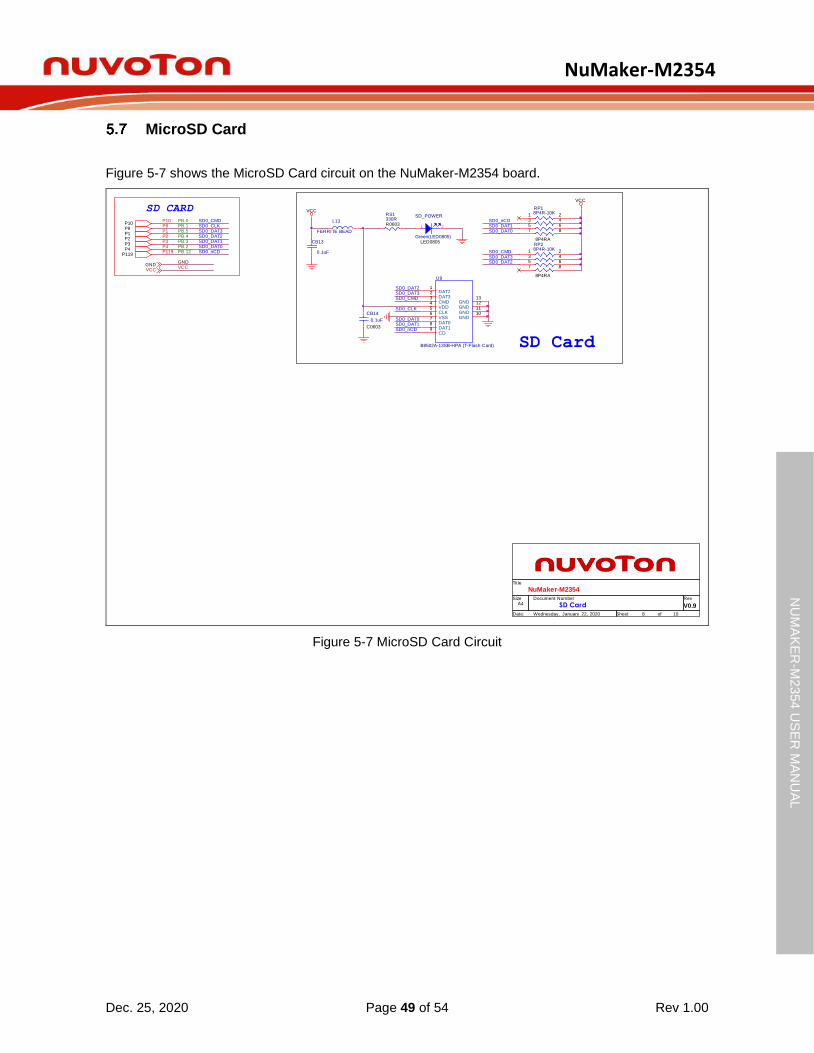
NuMaker-M2354
Dec. 25, 2020 Page 49 of 54 Rev 1.00
NU
MA
KE
R-M
2354 U
SE
R M
AN
UA
L
Maker N
u-m
bed
NU
C472 U
ser M
an
ual
MicroSD Card
Figure 5-7 shows the MicroSD Card circuit on the NuMaker-M2354 board.
Figure 5-7 MicroSD Card Circuit
Title
Size Document Number Rev
Date: Sheet of
NuMaker-M2354
V0.9SD CardA4
8 10Wednesday , January 22, 2020
SD CardSD0_nCD
SD0_DAT3
SD0_DAT1
SD0_DAT2
SD0_CMD
SD0_nCD
SD0_CMD
SD0_DAT0
SD0_DAT3
SD0_DAT2
SD0_CLK
SD0_DAT0
SD0_DAT1
CB13
0.1uF
RP28P4R-10K
8P4RA
1 23 45 67 8
L13
FERRITE BEAD
RS1330RR0603
U9
B8502A-13SB-HPA (T-Flash Card)
DAT21
DAT32
CMD3
VDD4
CLK5
VSS6
DAT07
DAT18
CD9
GND10GND11GND12GND13
1 2
SD_POWER
Green(LED0805)LED0805
CB14
0.1uF
C0603
RP18P4R-10K
8P4RA
1 23 45 67 8
VCC
VCC
PB.0P10 SD0_CMD
P9
P3
P10
PB.3P3 SD0_DAT1
PB.1P9 SD0_CLK
P4PB.12P119 SD0_nCDPB.2P4 SD0_DAT0
P1
P119
P1 PB.5 SD0_DAT3P2 PB.4 SD0_DAT2
SD CARD
VCC
P2
VCCGND
GND

NuMaker-M2354
Dec. 25, 2020 Page 50 of 54 Rev 1.00
NU
MA
KE
R-M
2354 U
SE
R M
AN
UA
L
Maker N
u-m
bed
NU
C472 U
ser M
an
ual
Wi-Fi Module (ESP-12)
Figure 5-8 shows the Wi-Fi Module (ESP-12) for wireless application on the NuMaker-M2354 board.
Figure 5-8 Wi-Fi Module Circuit
U2ESP-12
RST1
ADC2
EN3
IO164
IO145
IO126
IO137
VCC8
TXD22
RXD21
IO520
IO419
IO018
IO217
IO1516
GND15
CS
09
MIS
O10
IO9
11
IO1
012
MO
SI
13
SC
LK
14
URXD_ESP12UTXD_ESP12
C60.1uC0603
R310KRR0603
VCC
RST_ESP12
R510KRR0603
VCC VCC
R610KRR0603
R710KRR0603
URTS_ESP12
VCCIO0_ESP12
UCTS_ESP12 IO0_ESP12J5
HEADER 2.54 6X1 f emale (NC)
GPIO1
GND2
URXD_ESP12
GND
URTS_ESP12UCTS_ESP12
UTXD_ESP12
VCCGNDVCC
P18 PD.12IO0_ESP12
UART4_nRTSP46 PE.13
P17 PC.13RST_ESP12
UART4_TXDP48 PC.7
UART4_nCTSP47 PC.8
WIFI Off-page
UART4_RXDP49 PC.6
Title
Size Document Number Rev
Date: Sheet of
NuMaker-M2354
V0.9WIFI Module(ESP-12)A4
9 10Wednesday , January 22, 2020

NuMaker-M2354
Dec. 25, 2020 Page 51 of 54 Rev 1.00
NU
MA
KE
R-M
2354 U
SE
R M
AN
UA
L
Maker N
u-m
bed
NU
C472 U
ser M
an
ual
LCD interface
Figure 5-9 LCD interface Circuit shows the LCD connective interface and LCD panel for display application on the NuMaker-M2354 board.
Figure 5-9 LCD interface Circuit
SEG23 P62SEG24P60SEG25 P59SEG26P58SEG27 P57SEG28P56SEG29 P55SEG30P43
SEG2P109
SEG31 P42SEG32P41SEG33 P36SEG34P35SEG35 P34SEG36P33SEG37 P23SEG38P22
Title
Size Document Number Rev
Date: Sheet of
NuMaker-M2354
V1.1LCD interfaceA
2 10Monday , September 14, 2020
SEG3 P108SEG4P107
P91DH2
JLCD_1
HEADER 24X2 f emale
2468
1012141618202224262830323436384042444648
1357911131517192123252729313335373941434547
C_VLCD1uF
P90DH1
C_DH12(NC)0.1uF
GND
P[1:128]
LCD Off-page
SEG0P111
GND
P[1:128]
SEG1 P110
SEG5 P106
P92VLCD
SEG6P105SEG7 P102
SEG39 P21
SEG8P101SEG9 P100SEG10P99SEG11 P98SEG12P97SEG13 P85SEG14P84SEG15 P83COM0P74COM1 P73COM2P72COM3 P71COM4P70COM5 P69COM6P68COM7 P67SEG16P82SEG17 P81SEG18P80SEG19 P79SEG20P78SEG21 P77SEG22P63
U1
HTN LCD 8X40
COM522
COM724 COM623
SEG1625
SEG3241SEG3140SEG3039SEG2938SEG2837SEG2736SEG2635SEG2534SEG2433SEG2332SEG2231SEG2130SEG2029SEG1928SEG1827SEG1726
SEG12 SEG01
SEG67
SEG23
SEG34
SEG45
SEG56
SEG3342
SEG3443
SEG3544
SEG3645
SEG3746
SEG3847
SEG3948
COM017
COM118
COM219
COM320
SEG78
SEG89
SEG910
SEG1011
SEG1112
SEG1415
SEG1516
COM421
SEG121314
SEG13
SEG24P60SEG23 P62
SEG28P56SEG27 P57 SEG26P58SEG25 P59
SEG31 P42
SEG2P109
SEG30P43SEG29 P55
SEG35 P34 SEG34P35SEG33 P36 SEG32P41
SEG3 P108
SEG38P22SEG37 P23 SEG36P33
SEG4P107
JLCD_2
HEADER 24X2 male
2468
1012141618202224262830323436384042444648
1357911131517192123252729313335373941434547
SEG0P111
SEG7 P102 SEG6P105SEG5 P106
SEG1 P110
SEG10P99SEG9 P100 SEG8P101
SEG39 P21
SEG14P84SEG13 P85 SEG12P97SEG11 P98
COM2P72COM1 P73 COM0P74SEG15 P83
COM6P68COM5 P69 COM4P70COM3 P71
SEG18P80SEG17 P81 SEG16P82COM7 P67
SEG22P63SEG21 P77 SEG20P78SEG19 P79
SEG0
SEG2SEG1
SEG3SEG4
SEG6SEG5
SEG7SEG8
SEG10SEG9
SEG11SEG12
SEG14SEG13
SEG15
SEG16
SEG18SEG17
SEG19SEG20
SEG22SEG21
SEG23SEG24
SEG26SEG25
SEG27SEG28
SEG30SEG29
SEG31SEG32
SEG34SEG33
SEG35SEG36
SEG38SEG37
SEG39
COM0
COM4
COM2
COM6
COM1
COM5
COM3
COM7
Title
Size Document Number Rev
Date: Sheet of
LCD panel (8 COM x 40 SEG)
V1.0A
2 10Wednesday , April 08, 2020
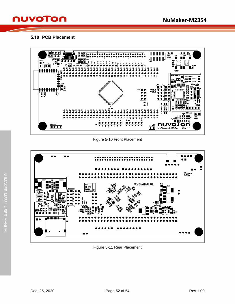
NuMaker-M2354
Dec. 25, 2020 Page 52 of 54 Rev 1.00
NU
MA
KE
R-M
2354 U
SE
R M
AN
UA
L
Maker N
u-m
bed
NU
C472 U
ser M
an
ual
PCB Placement
Figure 5-10 Front Placement
Figure 5-11 Rear Placement
NuMaker-M2354
Dec. 25, 2020 Page 53 of 54 Rev 1.00
NU
MA
KE
R-M
2354 U
SE
R M
AN
UA
L
Maker N
u-m
bed
NU
C472 U
ser M
an
ual
6 REVISION HISTORY
Date Revision Description
2020.12.25 1.00 1. Initially issued.

NuMaker-M2354
Dec. 25, 2020 Page 54 of 54 Rev 1.00
NU
MA
KE
R-M
2354 U
SE
R M
AN
UA
L
Maker N
u-m
bed
NU
C472 U
ser M
an
ual
Important Notice
Nuvoton Products are neither intended nor warranted for usage in systems or equipment, any malfunction or failure of which may cause loss of human life, bodily injury or severe property damage. Such applications are deemed, “Insecure Usage”.
Insecure usage includes, but is not limited to: equipment for surgical implementation, atomic energy control instruments, airplane or spaceship instruments, the control or operation of dynamic, brake or safety systems designed for vehicular use, traffic signal instruments, all types of safety devices, and other applications intended to support or sustain life.
All Insecure Usage shall be made at customer’s risk, and in the event that third parties lay claims to Nuvoton as a result of customer’s Insecure Usage, customer shall indemnify the damages and liabilities thus incurred by Nuvoton.