npl report mat 18 method for anisotropicpublications.npl.co.uk/npl_web/pdf/mat18.pdf · method for...
TRANSCRIPT

NPL REPORT MAT 18
On-wafer Testing of PCB Tracks as CPW Lines as a Production Assessment Method for Anisotropic Conductive Film Bonding M WICKHAM, M SALTER, N RIDLER, M DUSEK and C HUNT NOT RESTRICTED APRIL 2008


NPL Report MAT 18
On-wafer Testing of PCB Tracks as CPW Lines as a Production Assessment Method for Anisotropic Conductive Film Bonding
Martin Wickham, Martin Salter, Nick Ridler, Milos Dusek and Christopher Hunt Industry and Innovation Division
ABSTRACT To assess its suitability for production assessment of anisotropic conductive film (ACF) joints between flexible and rigid substrates, time domain reflectometery (TDR) characterisation, using a vector network analyser (VNA), of a range of differently bonded test samples has been undertaken. Based on the analysis of the reflected signal from various points on the sample, the aim was to interpret some factor that corresponded to the quality of the ACF joint. The high frequency electromagnetic TDR technique was able to successfully detect the bonding section joining the PCB lines including the beginning and ending of the bonded section along the length of the PCB lines. However, the technique was not able to detect any significant changes in the performance of the bonds due to ageing, nor was it able to detect the effect of graduated bonding pressure on the performance of the bonds. Some suggestions have been made for future investigations that could be undertaken to improve the sensitivity of this test system and test method so that changes due to ageing and/or bond pressure may become discernible.

NPL Report MAT 18
© Crown copyright 2008 Reproduced with the permission of the Controller of HMSO
and Queen’s Printer for Scotland
ISSN 1754-2979
National Physical Laboratory Hampton Road, Teddington, Middlesex, TW11 0LW
Extracts from this report may be reproduced provided the source is acknowledged and the extract is not taken out of context.
Approved on behalf of the Managing Director, NPL, by Dr M G Cain, Knowledge Leader, Materials Team
authorised by Director, Industry and Innovation Division

NPL Report MAT 18
CONTENTS
1 INTRODUCTION ..................................................................................................1
2 EXPERIMENTAL DETAILS ...............................................................................2 2.1 TEST VEHICLE...............................................................................................2 2.2 CHOICE OF PROBES .....................................................................................6
2.2.1 Bandwidth considerations.............................................................................6 2.3 VNA CALIBRATION......................................................................................9 2.4 TIME-DOMAIN.............................................................................................10
3 RESULTS ..............................................................................................................10 3.1 EXPERIMENT 1: MEASUREMENT OF AN UNBONDED PCB...............10 3.2 EXPERIMENT 2: BENCHMARK DATA FOR MATCHED AND
OPEN-CIRCUITED BONDED SAMPLES...................................................11 3.3 EXPERIMENT 3: EFFECTS OF AGEING ON BONDING
INTERCONNECTION...................................................................................13 3.4 EXPERIMENT 4: GRADUATED BONDING INVESTIGATION..............15
4 SUMMARY ...........................................................................................................18
5 ACKNOWLEDGMENTS....................................................................................19
6 REFERENCES .....................................................................................................19


NPL Report MAT 18
1
1 INTRODUCTION
Anisotropic conductive films (ACFs) have been widely used in electronics manufacturing for fine pitch interconnect for many years. Consisting of widely dispersed conductive spheres in an adhesive binder, they are bonded using temperature and pressure to trap the spheres between the raised surfaces of conductive tracks or bond pads on the substrates to be joined. This ensures electrical conduction in the z-axis, but the spheres are sufficiently isolated from each other to prevent conductive in the x and y axis’ (see Figure 1).
Substrate
Flexible
Compression load applied during bonding
Substrate
Flexible
Z-axis conduction path
Substrate
Flexible
Compression load applied during bonding
Substrate
Flexible
Z-axis conduction path
Figure 1: Example ACF bonding
The increased use of ACFs has been driven by their suitability for fine pitches. Their lighter weight compared to solders can also be used to advantage. Their low temperature fabrication has enabled them to be used in a wide range of applications where solder and particularly where the higher processing temperatures required by SnPb alternative solder alloys required under RoHS legislation [1], would be unsuitable. Available since the mid 1980’s, anisotropic conductive adhesives have found applications in tape automated (TAB) and flip-chip bonding, where they have the additional advantage as acting as an underfilling, thus negating the requirement for further processing [2]. Industrial applications have included smart cards, disk drives and graphics drivers. ACFs have found a particular niche market in packaging flat panel displays. Here the materials are used to interconnect a flexible circuit to both the glass backed display and the display driver PCB. Flat panel displays are utilised in an extraordinary range of applications from calculators and mobile phones through domestic white and brown goods, to PC monitors and televisions. Ruggedised versions have also found applications in military and avionics electronics. However, ACAs are still in their infancy when compared to the use of solders in electronics manufacture. Their conductivity can deteriorate over time particularly when subject to damp environments. Their impact strength has been shown to be poor and they tend to have a lower current carrying capacity when compared to solders [3]. There are also critical issues in manufacturing such as controlling the bonding pressure and temperature to ensure that sufficient mechanical and electrical contact are produced. Poor temperature control can lead to adhesion failures, moisture ingression and resistance increases. Insufficient pressure can lead to conductivity problems as the

NPL Report MAT 18
2
conductive spheres will have poor contact with the upper or lower substrates surfaces. Excessive bonding pressure can lead to crushing of the conductive spheres. Where these are metal-coated polymer spheres, this may result in rupturing of the plating and thus poor connectivity. If the bonding head is not planar, then either or both of these conditions can exist in a bond. Process control of the bonding process is limited. To ensure bond planarity, bonders can be characterised with pressure sensitive tapes to ensure even pressure across the bond. However, the industry does not have an in-process inspection tool to differentiate between acceptable and unacceptable bonds. Test methods are required as loss of performance, even in a single interconnect, is directly apparent to the end user as a non-functioning pixel on their flat panel display. Resistance testing can obviously be used to determine non-functioning joints, but no protocols are available to weed out joints which are likely to fail prematurely due to insufficient or excessive bonding pressures. The purpose of this work is to investigate the suitability of time-domain reflectometry for this task. High frequency electromagnetic TDR is primarily used in the electrical and electronics industries to characterize and locate faults in cabling such as twisted wire pairs or coaxial cables. Applications in testing of high speed PCBs are also under development. Conventional TDR transmits a fast rise time pulse along the conductor. The method used here involved synthesising the fast rise time pulse using a Vector Network Analyser (VNA) to generate a series of measurement points over a broad range of frequencies. For a well terminated conductor of uniform impedance, the pulse will be absorbed at the far-end of the termination and no signal will be reflected. However, any discontinuities in the conductor will produce echos that are reflected back. This is similar in principle to radar. 2 EXPERIMENTAL DETAILS
2.1 TEST VEHICLE To determine if the techniques under assessment were capable of differentiating between well and poorly bonded samples, test vehicles with three different levels of bonding planarity were fabricated. To mimic the bond between a flexible and a display driver PCB, the test vehicle consisted of an FR4 PCB with ENIG (electroless nickel/immersion gold) finished tracks bonded to a polyimide flexible, again with tracks finished in ENIG. The tracks, when bonded successfully, form a continuous meander, alternatively between PCB and flexible, across the width of the test vehicle. Test pads on the PCB allowed segments of the meander to be measured separately for comparison. For the TDR measurements, the end of the flexible and PCB were cropped as indicated in Figure 2, to provide a series of parallel tracks. The tracks were 125 μm wide with a 125 μm gap. The test vehicles were fabricated using 45μm thick, thermoplastic based ACF with 2μm diameter Ni particles. Bonding was typically at 180oC for 10 seconds at 2MPa pressure. Samples were fabricated with three different bonding planarities; (A) normal, (B) mild misalignment and (C) gross misalignment. Figure 3 shows a bond height scan using a

NPL Report MAT 18
3
laser profiling indicating a difference across the bond for a grossly misaligned sample of approximately 30μm.
Figure 2: ACF test vehicle
Figure 3: Laser surface scan of grossly misaligned test vehicle
Crop lines for TDR ACF bond area
180
190
200
210
220
230
240
250
260
270
0.75 1 1.25 1.5 1.75 2 2.25 2.5 2.75
Distance across ACF bond (cm)
Z di
men
sion
(mic
rons
)
NPL Report MAT 18
4
The test coupon consists of a series of nominally straight, parallel, metallic conductive tracks mounted on top of an insulating substrate. For any given set of three adjacent tracks, these can be viewed as a form of co-planar waveguide (CPW) transmission line [4, 5]. The two outer tracks provide the ground for the transmission line whereas the central track provides the signal carrying line. Therefore, this form of transmission line is often referred to as CPW with a Ground-Signal-Ground (GSG) configuration. The high frequency electromagnetic properties of such lines can be measured using GSG on-wafer probes connected to a Vector Network Analyser (VNA) [6]. When there are many such tracks, as with the test coupon shown in Figure 2, then adjacent sets of three tracks can be measured sequentially as a series of GSG CPW lines. So, for a series of n tracks, the following series of adjacent tracks can be measured in this way: (1, 2, 3), (2, 3, 4), . . . , (n – 2, n – 1, n). This results in a total of (n – 2) CPW lines being available for measurement. However, CPW lines formed in this way cannot be considered as truly independent of each other, since each track on the PCB will be used to form up to three CPW lines, i.e. twice as the Ground conductor and once as the Signal conductor. Therefore, in general, if one track is damaged in a way that affects its ability to act as part of a CPW line, then this is likely to affect measurements of three adjacent CPW lines that use the damaged track to form the lines. The test method used here relies on using a VNA configured to perform GSG CPW measurements using on-wafer probes. The VNA measures the reflection response, in terms of the magnitude of the complex-valued Voltage Reflection Coefficient (VRC), of each CPW line and displays the result in the time-domain (i.e. as a function of time). If the wave velocity, v, is known, then the magnitude (or amplitude) of the VRC, |VRC|, can be displayed as a function of distance, d, using:
2
tvd ×= (1)
where t is the displayed time and the factor 2 takes account of the there-and-back travel of the wave due to reflection. (The plots shown in this report include this factor 2 in the time axis, and so it is not used here when converting from time to distance.) The wave velocity, v, is given by:
*
r
cvε
= (2)
where εr
* is the effective relative permittivity of the dielectric of the CPW line and c is the speed of light in vacuo (= 299 792 458 ms-1). Since the dielectric, as ‘seen’ by the travelling electromagnetic wave, comprises effectively a combination of approximately 50 % air and 50 % PCB substrate, the effective relative permittivity, εr
*, can be estimated as the average of the relative permittivity of air and the PCB substrate material, i.e.:
NPL Report MAT 18
5
2
1 rr
ε+≈ε * (3)
where εr is the relative permittivity of the PCB substrate and 1 is the relative permittivity of air (to three significant figures).
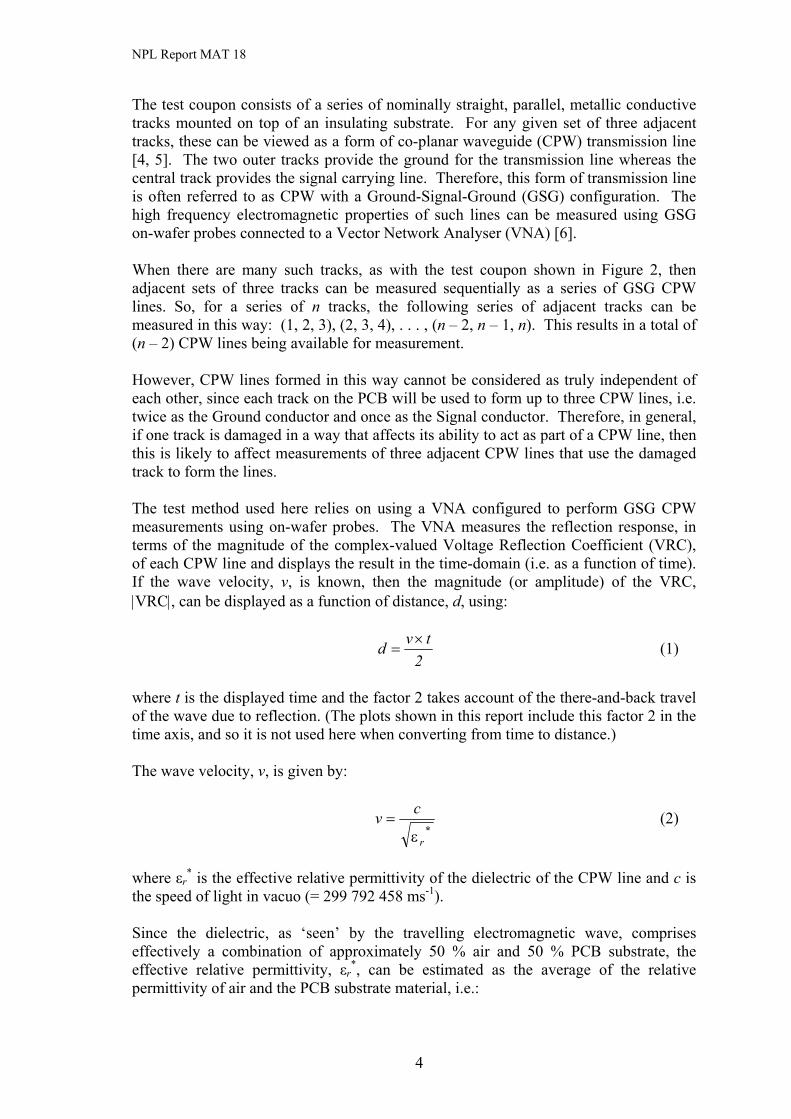
If the mechanical properties (physical dimensions, material construction, etc) of the line under test remain the same along the entire length of the line, then there will be no reflected signal as the wave travels along the line. This results in an observed |VRC| of zero. If, however, there is a change in the mechanical properties of the line (e.g. a discontinuity in the line) then an amount of signal will be reflected and the observed |VRC| becomes greater than zero. (By definition, 0 ≤ |VRC| ≤ 1.) In general, the larger the discontinuity, the larger the observed value of |VRC|. For example, a significant discontinuity will always occur at the interface between the on-wafer probe tip used to connect to the line and the CPW line under test, and this will be observed on the VNA as a reflection at t = d = 0. The purpose of the test described here is to investigate the quality of a join between two sets of tracks at a distance, D, along the line – see Figure 4. If the observed |VRC| at D is small, then the joining mechanism used for all (three) tracks forming the CPW line under test is expected to be of good quality. If the observed |VRC| at D is large, then the joining mechanism on any one (or more than one) track forming the CPW line under test is expected to be of poor quality.
Figure 4: Interconnect under test joining rigid and flexible PCBs. The join occurs at a distance D along the line
The observed |VRC| can be interpreted as a measure of the broadband resistance (or, more generally, impedance) of the joint. It therefore gives an indication of the performance of the join when operating over a wide range of frequencies. For example, high-speed digital waveforms comprise a broad spectrum of frequency components, so a large |VRC| observed during this test suggests that such waveforms may become distorted or significantly attenuated as they pass through the join.
D

NPL Report MAT 18
6
2.2 CHOICE OF PROBES A key parameter that needs to be considered when using on-wafer probes is the pitch of the probe. This is a measure of the separation between the adjacent fingers of the probe that are used to make contact with the conductors of the CPW. Figure 5 gives a close-up view of a GSG probe tip and shows the contact fingers.
Figure 5: A close-up view of a GSG CPW probe tip
The separation between adjacent tracks on the test coupon was approximately 500 μm and so a probe with a pitch of 500 μm was chosen for the measurements. This ensured that the probe would land close to the centre of each of the tracks comprising the CPW lines formed on the test coupon. Figure 6 shows a photo of a typical probe used for this type of measurement. This shows the GSG probe tip as well as the coaxial connector used to connect the probe, via a coaxial cable, to the VNA. Most of the probe consists of a mechanism for transforming from the coaxial input section to the GSG CPW output section.
Figure 6: A typical CPW on-wafer probe
2.2.1 Bandwidth considerations Before performing measurements of the test coupon, it is first necessary to establish the bandwidth, i.e. frequency range, for the test measurements. This bandwidth is restricted
Ground
Signal
Ground
GSG probe tip
Coaxial connector
NPL Report MAT 18
7
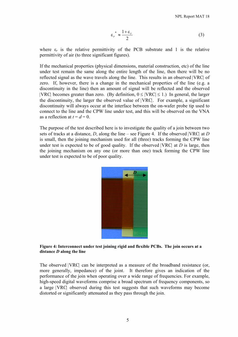
by either the bandwidth of the measuring system (VNA, calibration standards, cables and probes) and/or the bandwidth of the CPW lines formed on the test coupon. In the case of the measuring system, the cables, calibration standards and probes were chosen so that their bandwidth exceeded, or was at least equal to, the bandwidth of the VNA. The bandwidth of the VNA used for these measurements was 40 MHz to 40 GHz. Figure 7 shows a photo of the overall test set-up comprising probe, probe station, test cables and VNA.
Figure 7: The complete measurement system: VNA (right-hand-side); probe station (centre); and, probe/test coupon (immediately below the microscope)
In the case of the CPW lines, the bandwidth is constrained by the frequency range over which a single electromagnetic mode can be expected to propagate, i.e. below the frequency at which higher-order modes may be expected to propagate [7]. This is because if frequencies are used for the test where higher-order modes are propagating, then the measurements may become unreliable and unrepeatable. Higher-order mode behaviour occurs in all forms of transmission line and has been studied in detail in the literature [8, 9]. For example, studies in coaxial lines (see, for example, [10]) have shown that the onset of higher-order modes results in an increase in both return and insertion loss (i.e. an increase in reflected signal and a decrease in transmitted signal). In addition, the amount of reflected and transmitted signal varies considerably as the connection to a device is broken then remade. This is illustrated in Figure 8, which shows the magnitude of the change in VRC due to disconnecting and reconnecting a pair of precision coaxial connectors with a rated upper operating frequency of 18 GHz. Below 18 GHz the observed variation is very small whereas above 18 GHz the variation rises dramatically.

NPL Report MAT 18
8
Lin 0.10
0.09
0.08
0.07
0.06
0.05
0.04
0.03
0.02
0.01
0.00
S11
Start: 45.000000 MHz Stop: 26.500000 GHz
1
1 18.034400 GHz 1.3015 mLin
Figure 8: Magnitude of measured change in VRC as a function of frequency, due to disconnecting and reconnecting a pair of coaxial connectors
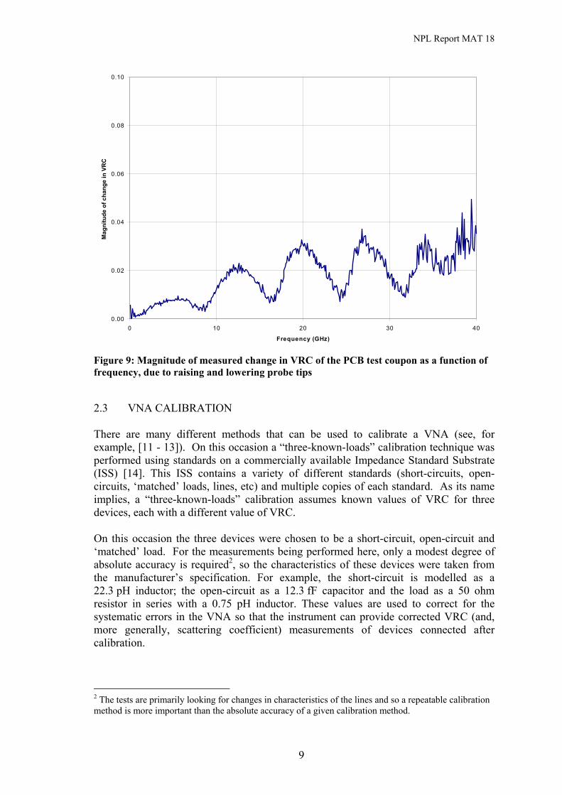
A similar test was made on the PCB test coupon used here by making repeated connections with the on-wafer probe. These tests were performed using the full bandwidth of the VNA (i.e. to 40 GHz). A result from these tests is shown in Figure 9. This does not show the onset of a significant lack of repeatability across this frequency range.1 This suggests that significant amounts of higher-order modes are not being stimulated at frequencies up to 40 GHz. It is therefore considered safe to interpret measurements made over this full bandwidth. (At some higher frequency, it is almost certain that higher-order modes will begin to cause problems with measurements on these lines, but the frequency at which this is expected to occur is above the 40 GHz limit of this test set-up.)
1 The slow undulating ripple seen on this trace is likely to be caused by variations in probe contact impedance interacting with post-calibration residual errors in the VNA. Such behaviour is to be expected for this type of measurement.
NPL Report MAT 18
9
0.00
0.02
0.04
0.06
0.08
0.10
0 10 20 30 40
Frequency (GHz)
Mag
nitu
de o
f cha
nge
in V
RC
Figure 9: Magnitude of measured change in VRC of the PCB test coupon as a function of frequency, due to raising and lowering probe tips
2.3 VNA CALIBRATION There are many different methods that can be used to calibrate a VNA (see, for example, [11 - 13]). On this occasion a “three-known-loads” calibration technique was performed using standards on a commercially available Impedance Standard Substrate (ISS) [14]. This ISS contains a variety of different standards (short-circuits, open-circuits, ‘matched’ loads, lines, etc) and multiple copies of each standard. As its name implies, a “three-known-loads” calibration assumes known values of VRC for three devices, each with a different value of VRC. On this occasion the three devices were chosen to be a short-circuit, open-circuit and ‘matched’ load. For the measurements being performed here, only a modest degree of absolute accuracy is required2, so the characteristics of these devices were taken from the manufacturer’s specification. For example, the short-circuit is modelled as a 22.3 pH inductor; the open-circuit as a 12.3 fF capacitor and the load as a 50 ohm resistor in series with a 0.75 pH inductor. These values are used to correct for the systematic errors in the VNA so that the instrument can provide corrected VRC (and, more generally, scattering coefficient) measurements of devices connected after calibration.
2 The tests are primarily looking for changes in characteristics of the lines and so a repeatable calibration method is more important than the absolute accuracy of a given calibration method.

NPL Report MAT 18
10
2.4 TIME-DOMAIN Most modern VNAs include a facility for transforming a frequency-domain measurement response into an equivalent time-domain response. The technique is based on the application of Fourier analysis [15], which relates mathematically a response as a function of frequency to a response as function of time. For a VNA, the frequency-domain response consists of a series of discrete frequency points. If there are N frequency points, f0, f1, . . . , fN-1, let the mth measured VRC, Γ, at frequency fm be Γ(fm), then the inverse discrete Fourier transform used to compute the time-domain response, γ(tn), is given by:
∑Γ=γ=
πN
k
Nnkj
mn e)f(N
)t(0
21
Computational details of this transformation are given in [16]. The specific variety of transformation used in the VNA is the Chirp z-transform, a full description of which is given in [17]. This transform, so called because the input signal resembles a “chirp” waveform3 used in some radar systems, has been used extensively in many areas of spectral and frequency analysis. It is used in this investigation in Time Band Pass mode, as this mode of operation is simple to use and is less likely to yield spurious responses. Some guidance on using a VNA in Time Band Pass mode is given in [18], and its successful operation has been demonstrated previously in [19]. 3 RESULTS Results are shown for four different experiments:
1. Measurement of an unbonded PCB; 2. Benchmark data for ‘matched’ and open-circuited bonded samples; 3. Effects of ageing on bonding interconnection; 4. Graduated bonding investigation.
3.1 EXPERIMENT 1: MEASUREMENT OF AN UNBONDED PCB Some typical results for a section of unbonded ‘rigid’ PCB of approximately 13 mm in length are shown in Figure 10. Moving from left to right along the horizontal axis of this Figure, the first observed peak occurs at approximately 0 ps. This corresponds to the position of the launch of the test signal onto the PCB, i.e. where the probe tip touches the PCB. This form of ‘interconnect’ produces a discontinuity, the size of which should be similar for each probe/PCB connection. This discontinuity is observed here to be |VRC | ≈ 0.27. A similar value of |VRC | at t = 0 is expected for all subsequent test results reported here.
3 A “chirp” waveform is one whose frequency increases continuously with time.

NPL Report MAT 18
11
0
0.1
0.2
0.3
0.4
0.5
0.6
0.7
0.8
-100 -50 0 50 100 150 200 250 300 350 400
Time (pS)
Line
ar m
agni
tude
VR
C
Figure 10: Time-domain assessment of an unbonded PCB. The peaks are caused by observed reflections on the PCB
The second peak, occurring at approximately 65 ps and of |VRC| ≈ 0.7, corresponds to the position of the end of the PCB. This forms effectively an open-circuit and causes almost all the remaining electromagnetic energy to be reflected back along the CPW line. If we assume the relative permittivity of the substrate of this PCB is approximately equal to 4.4, then we can use equations (1) to (3) to estimate the distance from the probe contact point to the end of the PCB, i.e. d ≈ 12 mm. This agrees with the approximate physical length of the PCB, measured using a ruler, and so provides some assurance when interpreting the peaks in this, and subsequent, Figures. The other peaks occurring at approximately 130 ps and 200 ps are due to multiple reflections caused by interactions between the two previous peaks. These peaks are of no real significance concerning the investigation reported here.
3.2 EXPERIMENT 2: BENCHMARK DATA FOR MATCHED AND OPEN-CIRCUITED BONDED SAMPLES
Measurements were made on some ‘rigid’ PCBs where a section of flexible PCB has been attached using the bonding process that forms the subject of this investigation. Figure 11 shows a diagram of this form of ‘bonded’ PCB. Some typical results are shown in Figure 12 and Figure 13 for two PCBs. One of these PCBs had some resistive material applied to the end of the flexible section of PCB. This was an attempt to reduce the amount of signal reflected back by the otherwise open-circuited line. The results for the PCB containing resistive material are shown in Figure 12 whereas the results for the open-circuited PCB are shown in Figure 13.

NPL Report MAT 18
12
0
0.05
0.1
0.15
0.2
0.25
0.3
0.35
0.4
0.45
0.5
-100 -50 0 50 100 150 200 250 300 350 400
Time (pS)
Line
ar m
agni
tude
VR
C
Figure 12: Time-domain assessment of a bonded PCB sample. This sample contained resistive material at the end of the flexible PCB to help absorb some of the reflected energy
Rigid PCB
Flexible PCB Bonded section
Start Stop
Figure 11: Diagram of the cross-section of a bonded PCB sample. This shows: the rigid PCB (on the left); the flexible PCB (on the right); and, the bonding section (in the middle). The Start and Stop positions of the bonded sections are also shown. (This diagram is not drawn to scale.)

NPL Report MAT 18
13
0
0.05
0.1
0.15
0.2
0.25
0.3
0.35
0.4
0.45
0.5
-100 -50 0 50 100 150 200 250 300 350 400
Time (pS)
Line
ar m
agni
tude
VR
C
Figure 13: Time-domain assessment of a bonded PCB sample. The flexible PCB on this sample was left open-circuited
Both these figures show a small peak (or disturbance) at around 40 ps (i.e. a distance of approximately 8 mm from the beginning of the line). This distance agrees well with the start point of the bonded section shown in Figure 11. The larger peak at around 65 ps (i.e. a distance of approximately 12 mm from the beginning of the line) corresponds as before to the end of the PCB. The larger peak at around 120 ps is produced by the end of the flexible PCB. The amplitude of the peak in Figure 13 is greater (|VRC | ≈ 0.42) than for the sample in Figure 12 as there is no resistive element to absorb the signal. This shows that this test is detecting the bonded section. A small peak is seen at approximately 90ps, and this could be (if real) due to some anomaly in the flex half way between the joint and the end of the flex. An anomaly could be a crease or change in cross section. No artefacts were identified in the sample and the source of this peak remains unknown.
3.3 EXPERIMENT 3: EFFECTS OF AGEING ON BONDING INTERCONNECTION
Both resistively terminated and open-circuits PCBs were subjected to an ageing process. The results for both resistively terminated and open-circuited PCBs showed similar trends and so only the open-circuited results are given here. Figures 14, 15 and 16 show the performance of the same PCB after 340 hours, 640 hours and 1000 hours of ageing, respectively. Of main interest in these Figures is the behaviour of the two previously identified peaks occurring at approximately 40 ps and 65 ps, as these correspond to the position of the bonded section of the PCBs. There is no obvious difference between these peaks in these Figures and so it is concluded that either the performance of the PCBs is not changing significantly as a result of this ageing process, or the test method is not able to detect any change in performance due to this ageing.

NPL Report MAT 18
14
0
0.05
0.1
0.15
0.2
0.25
0.3
0.35
0.4
0.45
0.5
-100 -50 0 50 100 150 200 250 300 350 400
Time (pS)
Line
ar m
agni
tude
VR
C
Figure 14: Bonded PCB sample after 340 hours of ageing
0
0.05
0.1
0.15
0.2
0.25
0.3
0.35
0.4
0.45
0.5
-100 -50 0 50 100 150 200 250 300 350 400
Time (pS)
Line
ar m
agni
tude
VR
C
Figure 15: Bonded PCB sample after 640 hours of ageing

NPL Report MAT 18
15
0
0.05
0.1
0.15
0.2
0.25
0.3
0.35
0.4
0.45
0.5
-100 -50 0 50 100 150 200 250 300 350 400
Time (pS)
Line
ar m
agni
tude
VR
C
Figure 16: Bonded PCB sample after 1000 hours of ageing
3.4 EXPERIMENT 4: GRADUATED BONDING INVESTIGATION All the traces shown in Figures 12 to 16 show a significant ‘blurring’ with regard to the observed height of each of the peaks. This blurring is caused by the different GSG CPW lines formed on the PCB having a slightly different value of |VRC| at the same position along the lines. To investigate this further, the 65ps peak in Figure 12 was selected and the height of each trace forming the peak was plotted as a function of GSG CPW line number. An example of such a plot is shown in Figure 17. This effectively shows that the impedance of the bond varies across the PCB, which in turn suggests that the quality of the bond appears to vary systematically across the PCB.

NPL Report MAT 18
16
0
0.1
0.2
0.3
0.4
0.5
0 10 20 30 40 50
Transmission line number
Mag
nitu
de V
RC
at s
elec
ted
peak
Figure 17: A plot showing how the height of a given peak varies as a function of CPW line number Based on the above observation, three bonded samples were fabricated with varying amounts of graduated applied pressure used when forming the bond:
i) no graduated pressure; ii) a mild amount of graduated pressure; iii) a significant amount of graduated pressure.
Each sample was tested without ageing. The results are shown in Figures 18 to 20. These results do not show any obvious difference between these Figures (at 40 ps and 65 ps) and so it is concluded that either the PCBs are not changing significantly as a result of varying the bonding pressure, or that the test method is not able to detect any change in performance of the bond due to varying the bonding pressure.

NPL Report MAT 18
17
0
0.1
0.2
0.3
0.4
0.5
0.6
-100 -50 0 50 100 150 200 250 300 350 400
Time (pS)
Line
ar m
agni
tude
VR
C
Figure 18: Sample A1, bonded using un-graduated bonding pressure
0
0.1
0.2
0.3
0.4
0.5
0.6
-100 -50 0 50 100 150 200 250 300 350 400
Time (pS)
Line
ar m
agni
tude
VR
C
Figure 19: Sample B1, bonded using a mild amount of graduated bonding pressure

NPL Report MAT 18
18
0
0.1
0.2
0.3
0.4
0.5
0.6
-100 -50 0 50 100 150 200 250 300 350 400
Time (pS)
Line
ar m
agni
tude
VR
C
Figure 20: sample C1, bonded using a significant amount of graduated bonding pressure
4 SUMMARY From the above investigation, the following conclusions can be drawn concerning the use of a high frequency electromagnetic time-domain technique:
1. The technique was able to successfully detect the bonding section joining the PCB lines. n fact the technique was able to detect the beginning and ending of the bonded section along the length of the PCB lines;
2. The technique was not able to detect any significant changes in the performance of the bonds due to ageing;
3. The technique was not able to detect the effect of graduated bonding pressure on the performance of the bonds.
Potential future investigations that could be undertaken to improve the sensitivity of this test system and test method so that changes due to ageing and/or bond pressure may become discernible, include:
1. Perform tests using different signal bandwidths; 2. Use a more sophisticated form of time-domain analysis (e.g. low-pass step
and/or impulse modes); 3. Use time-domain signal processing (e.g. gating and windowing functions to
help isolate features of interest); 4. Look at the transmitted as well as the reflected properties of the PCBs; 5. Look at the PCB tracks as differential transmission lines. This could lead to
simultaneous testing of many tracks using a multi-port VNA approach; 6. Use a better (i.e. lower |VRC|) system to connect the test system to the
PCBs.

NPL Report MAT 18
19
5 ACKNOWLEDGMENTS The work was carried out as part of a project in the Processing Programme of the UK Department Innovation Universities and Skills. We gratefully acknowledge the support and co-operation of Martin Barthlomew and Steve Riches, of GE Dyamnics. 6 REFERENCES [1] DIRECTIVE 2002/95/EC OF THE EUROPEAN PARLIAMENT AND OF
THE COUNCIL of 27 January 2003 on the restriction of the use of certain hazardous substances in electrical and electronic equipment; http://www.rohs.gov.uk/Docs/Links/RoHS%20directive.pdf
[2] Kivilahti J.K. and Savolainen P.: Design and modelling of solder-filled ACAs
for flip-chip and flexible circuit applications; Conductive adhesives for electronics packaging, edited by Johan Lui, Electrochemical publications 1999, ISBN 0 901150 37 1
[3] Fan, S. H. and Chan, Y. C.; Current-carrying capacity of anisotropic-conductive
film joints for the flip chip on flex applications; Journal of Electronic Materials, Feb 2003
[4] Gupta, K. C. et al; Microstrip lines and slotlines, 2nd Ed, Artech House,
Norwood MA, 1996. [5] Simons, R. N.; Coplanar waveguide circuits, components and systems, Wiley
Interscience, New York, 2001 [6] Lucyszyn, S.; RFIC and MMIC measurement techniques, in “Microwave
Measurements” chapter 11, in “Microwave Measurements”, 3rd edition, Institution of Engineering and Technology, Electrical Measurement Series 12, edited by R J Collier and A D Skinner, pp 217-262, 2007.)
[7] Riaziat, M. et al; Propagation modes and dispersion characteristics of coplanar
waveguides, IEEE Trans. MTT, Vol. 38, No. 3, pp 245-251, March 1980 [8] Marcuvitz, N.; Waveguide Handbook, MIT Radiation Laboratory Series,
Vol 10, McGraw Hill, New York, 1951. [9] Ramo, S. and Whinnery, J.; Fields and Waves in Modern Radio, John Willey
and Sons, Inc, New York, 1956. [10] Gilmore, J. F.; TE11-mode resonances in precision coaxial connectors, GR
Experimenter, Vol 40, No 8, pp 10-13, August 1966. [11] Rumiantsev, A. and Ridler, N.; Vector Network Analyzer Calibration, accepted
for publication, IEEE Microwave Magazine, June 2008

NPL Report MAT 18
20
[12] Rytting, D.; An analysis of vector measurement accuracy enhancement techniques, RF & Microwave Symposium and Exhibition, Hewlett Packard, Santa Rosa, CA, USA, 1980.
[13] Marks, R. B.; Formulations of the basic vector network analyzer error model
including switch terms, 50th ARFTG conference digest, pp 115-126, December 1997.
[14] Calibration Substrate Part Number CS-9, GGB Industries Inc, Naples, FL, USA.
(www.picoprobe.com). [15] Brigham, E. O.; The Fast Fourier Transform and its applications, Prentice-Hall,
1988. [16] Press, W. H., Flannery, B. P., Teukolsky, S. A. and Vetterling, W. T.; Numerical
Recipes, Cambridge University Press, 1988 [17] Rabiner, L. R., Schafer, R. W. and Rader, C. M.; The Chirp z-transform
algorithm and its application, Bell System Tech J (USA), Vol 48, pp 1249-1292, May-June 1969.
[18] Ridler, N. M. (Ed); Time domain analysis using network analysers: some good
practice tips, ANAMET Report 027, September 1999. [19] Horibe, M. and Ridler, N.; Using time-domain measurements to improve
assessments of precision coaxial air lines as standards of impedance at microwave frequencies, 70th ARFTG Microwave Measurement Conference digest, pp 84-90, Tempe, AZ, USA, November 2007.