novel adder circuits based on quantum-dot cellular ...file.scirp.org/pdf/cs_2014061314463612.pdf ·...
TRANSCRIPT
Circuits and Systems, 2014, 5, 142-152 Published Online June 2014 in SciRes. http://www.scirp.org/journal/cs http://dx.doi.org/10.4236/cs.2014.56016
How to cite this paper: Ahmad, F., Bhat, G.M. and Ahmad, P.Z. (2014) Novel Adder Circuits Based on Quantum-Dot Cellular Automata (QCA). Circuits and Systems, 5, 142-152. http://dx.doi.org/10.4236/cs.2014.56016
Novel Adder Circuits Based on Quantum-Dot Cellular Automata (QCA) Firdous Ahmad1*, Ghulam Mohiuddin Bhat1, Peer Zahoor Ahmad2 1Department of Electronics & IT, University of Kashmir, (J&K) India 2Department of Computer Science University of Kashmir, (J&K) India Email: *[email protected] Received 2 April 2014; revised 3 May 2014; accepted 11 May 2014
Copyright © 2014 by authors and Scientific Research Publishing Inc. This work is licensed under the Creative Commons Attribution International License (CC BY). http://creativecommons.org/licenses/by/4.0/
Abstract Quantum-dot cellular automaton (QCA) is a novel nanotechnology that provides a very different computation platform than traditional CMOS, in which polarization of electrons indicates the digi-tal information. This paper demonstrates designing combinational circuits based on quantum-dot cellular automata (QCA) nanotechnology, which offers a way to implement logic and all intercon-nections with only one homogeneous layer of cells. In this paper, the authors have proposed a novel design of XOR gate. This model proves designing capabilities of combinational circuits that are compatible with QCA gates within nano-scale. Novel adder circuits such as half adders, full ad-ders, which avoid the fore, mentioned noise paths, crossovers by careful clocking organization, have been proposed. Experiment results show that the performance of proposed designs is more efficient than conventional designs. The modular layouts are verified with the freely available QCADesigner tool.
Keywords Quantum Dot Cellular Automata (QCA), XOR Gate, Half Adder, Full Adder, Nanotechnology, QCADesigner
1. Introduction Quantum-dot cellular automaton (QCA) is a new nanotechnology that can help us to achieve low power con-sumption, high device density, and high clock frequency. Since QCA, size is smaller than CMOS it can, even be implemented in molecular or atomic size. Further, in CMOS, by decreasing the transistor sizes, some problems such as power consumption cannot be ignored. A number of research efforts have been focused on new devices
*Corresponding author.
F. Ahmad et al.
143
that might replace CMOS technology [1]. Utilizing the QCA technology [2] for implementing logic circuits is one of the approaches which, in addition to decreasing the size of logic circuits and increasing the clock fre-quency and reduces the power consumption of these circuits. The emerging technologies pertaining to circuit design lay great emphasis on small size, high device density, and low power dissipation to achieve objective of portability of systems [3]. Quantum-dot Cellular Automata (QCA) [4] [5], promises aforementioned features.
The implementation of circuits using QCA is based on coulombic interactions. QCA circuits can be used to implement combinational circuits by arranging cells with proper clock delays. So far, several studies have been reported about QCA full adder [6]-[12]. Initial adder designs were constructed with five majority gates (a fun-damental QCA logic gate) and three inverters [11]. Tougaw and Lent proposed the first design for a QCA 1-bit full adder by connecting “n”, such 1-bit QCA full adders, a carry look ahead (CLA) adder can be obtained, since the carry is generated before the sum in the QCA adder [13]. A new bitserial QCA adder has also been proposed [14], which uses carry feedback and only requires three majority gates and two inverters. However, this bit-serial approach requires a complicated clocking scheme and feedback control. In this paper, we propose an efficient XOR gate with proper clock delay organizations which has been presented. The present design consists of less area to conventional designs [15].
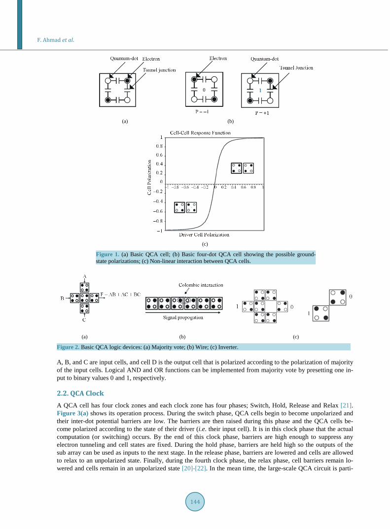
2. Quantum-Dot Cellular Automata (QCA) The fundamental unit of QCA device is QCA cell. A QCA cell, created with four quantum Dots positioned at the vertices of a square [16] [17], coupled by tunneling barriers has been in Figure 1(a). These quantum dots are sites in which electrons are able to tunnel between them but cannot leave the cell. The electrons will tend to oc-cupy diagonally opposite sites into the quantum dots due to electrostatic force of interaction.
Quantum dots are small semi-conductor or metal islands with a diameter that is small enough to make their charging energy greater than kbT (where kb is Boltzmann’s constant and T is the operating temperature).
Two mobile electrons are loaded in the cell, which can move to different quantum dots in the QCA cell by means of electron tunneling. The lines connecting the quantum dots in Figure 1(b) can represent tunneling paths. The electrons in the cell, placed adjacent to each other will interact; as a result, the polarization of one cell will be directly affected by the polarization of its neighboring cells.
If the barriers between cells are sufficiently high, the electrons will be well localized in individual dots. The Coulomb repulsion between the electrons will tend to make them occupy antipodal sites in the square as shown in Figure 1(b). For an isolated cell there are two energetically equivalent arrangements of the extra electrons which we denote as a cell polarization P = +1 and P = −1. The term “cell polarization” refers only to this ar-rangement of charge and does not imply a dipole moment for the cell. The cell polarization is used to encode binary information, thus, P = +1 represents a binary 1 and P = −1 represents a binary 0. The two polarization states of the cell will not be energetically equivalent if other cells are nearby. Consider two cells close to one another as shown in the inset of Figure 1(c). It illustrates the case when cell 2 has a polarization of P = +1 state, the ground-state configuration of cell 1 follows the same polarization. Similarly if cell 2 is in the P = −1 state, the ground state of cell 1 will match it. This shows the nonlinear response of the cell–cell interaction, which plays the role of voltage gain in conventional devices.
In QCA implementations, the power consumption of QCA circuits is mainly affected by clock signals. Therefore, in practice using a proper clock, the power consumption will be very less but still it is data dependent. In order to remove the data dependency of power traces, Bennett clocking scheme can be used for different in-puts [18]. By using Bennett clocking, the power dependence of QCA circuits on the inputs can be effectively removed making it impossible to perform power analysis attack [19].
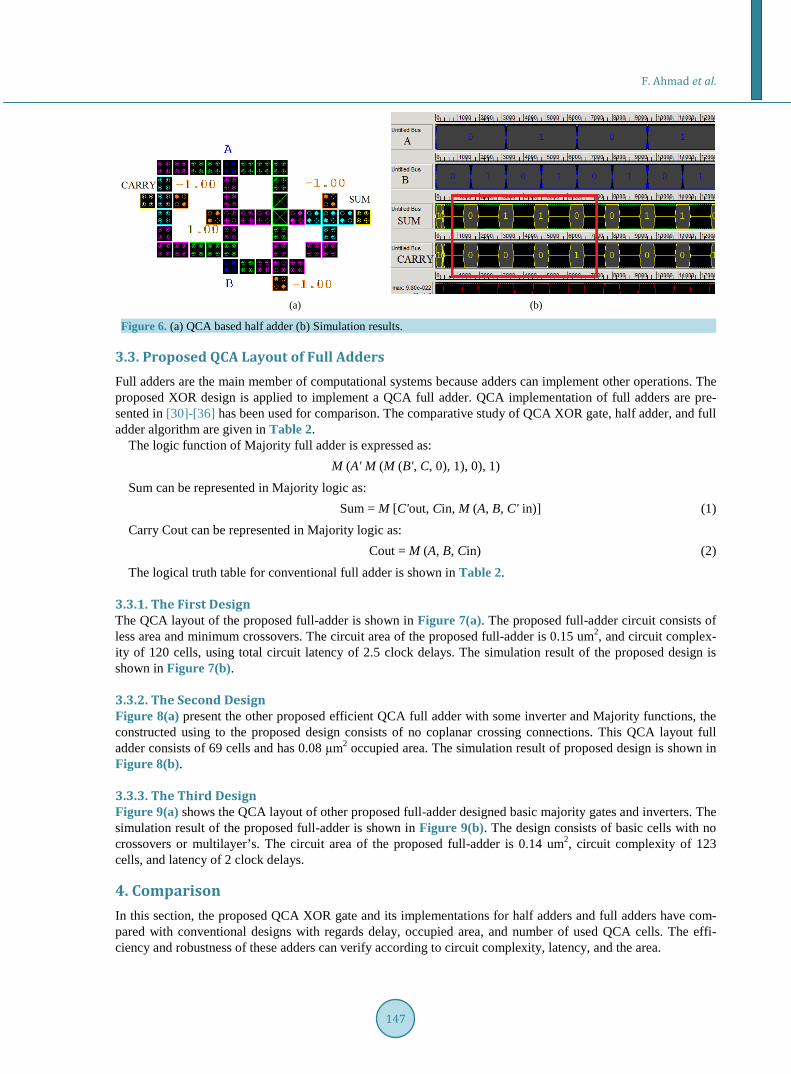
2.1. QCA Logic Circuits Some basic elements for QCA logic implementation are wire, inverter, and majority voter [20] shown in Figure 2(a), Figure 2(b) & Figure 2(c). The QCA wire is formed by an array of QCA cells shown in Figure 2(b), which provides a medium for data propagation based on Coulomb interactions. The simplest inverter is built by placing QCA cells in a diagonal structure shown in Figure 2(c). The polarization of the output QCA cell “out” or “output” is the opposite of the polarization of input QCA cell “in” or “input”. Here the MV, is equivalent to a logic function F (A, B, C) =AB + AC + BC and can be implemented by five QCA cells arranged in a cross. Cells
F. Ahmad et al.
144
(a) (b)
(c)
Figure 1. (a) Basic QCA cell; (b) Basic four-dot QCA cell showing the possible ground- state polarizations; (c) Non-linear interaction between QCA cells.
(a) (b) (c)
Figure 2. Basic QCA logic devices: (a) Majority vote; (b) Wire; (c) Inverter. A, B, and C are input cells, and cell D is the output cell that is polarized according to the polarization of majority of the input cells. Logical AND and OR functions can be implemented from majority vote by presetting one in-put to binary values 0 and 1, respectively.
2.2. QCA Clock A QCA cell has four clock zones and each clock zone has four phases; Switch, Hold, Release and Relax [21]. Figure 3(a) shows its operation process. During the switch phase, QCA cells begin to become unpolarized and their inter-dot potential barriers are low. The barriers are then raised during this phase and the QCA cells be-come polarized according to the state of their driver (i.e. their input cell). It is in this clock phase that the actual computation (or switching) occurs. By the end of this clock phase, barriers are high enough to suppress any electron tunneling and cell states are fixed. During the hold phase, barriers are held high so the outputs of the sub array can be used as inputs to the next stage. In the release phase, barriers are lowered and cells are allowed to relax to an unpolarized state. Finally, during the fourth clock phase, the relax phase, cell barriers remain lo-wered and cells remain in an unpolarized state [20]-[22]. In the mean time, the large-scale QCA circuit is parti-

F. Ahmad et al.
145
tioned into four clock zones; Figure 3(b) shows each clock zone signal and demonstrates pipeline mechanism. All cells in a certain zone are controlled by the same QCA clock signal. Cells in each zone perform a specific calculation; the state of a zone is then fixed so that it can serve as input signal to the next zone. This results into information transfers in a pipelined fashion.
3. QCA Implementations In addition to basic logic gates, exclusive-OR (XOR) and exclusive-NOR (XNOR) gates are also used in the de-sign of digital circuits. These have special functions and applications. These gates are particularly useful in arithmetic operations as well as code generators. XOR and XNOR gates are usually found as 2-input gates. No multiple-input XOR/XNOR gates are available since they are complex to fabricate with hardware. Different au-thors have proposed QCA XOR gates for conventional layout [23]-[25]. The design has complexity of cells and coplanar crossovers or multiple layers to implement. The area of these conventional designs is large. The per-formance of various QCA layouts XOR gates has been shown in [26].
3.1. Proposed XOR Gate It is possible to implement all combinational and sequential logic functions by properly arranging cells so that the polarization of one cell sets the polarization of a nearby cell [27]. According to previous studies, several logic gates and computing devices [28] are implemented with QCA. We propose an efficient XOR gates with less crossovers, area 0.03 μm2, of 30 cells and 0.5 clock delays as shown in Figure 4(a) compared to previous designs [26]. The simulation results of proposed XOR gate is shown in Figure 4(b).
(a) (b)
Figure 3. (a) Four phases of QCA clock; (b) Clock zones signal.
(a) (b)
Figure 4. (a) QCA layout of XOR gate; (b) Simulation results.

F. Ahmad et al.
146
3.2. Proposed QCA Layout of Half Adders Digital computers perform various arithmetic operations. The most basic operation is the addition. The addition operation is achieved by majority logic that can reduce the overall number of gates required to create the adder circuits. Researchers have proposed the QCA implementation of half adder [29]. The design needs either copla-nar crossovers or multiple layers to implement. The half adder is a combinational circuit that performs addition of two bits. It is designed conventionally by XOR and AND gates. When two inputs A and B are added, the Sum and Carry outputs are produced. The truth table of conventional half adder is shown in Table 1. The logic func-tion for half adder is:
Sum = A'.B + A.B' which is exclusive-OR (XOR) function Carry = A.B, which is an (AND) function
Thus, QCA majority logic can be written as: Sum = m (m (A', B, 0), 1) Carry = m (m (A, B, 0))
3.2.1. The First Design QCA based half adder circuit proposed in this paper has been shown in Figure 5(a). A simulation result of the proposed design is shown in Figure 5(b). The simulation results of this gate have been checked using QCADe-signer. The circuit is designed with the regular arrangement of QCA cells with proper latency. The proposed half-adder consists of 27 cells, area 0.03 um2 and latency 0.5 clock delays, which is less as compared to [27]- [29]. The simulation results of novel half adder circuits have been checked with Table 1. The advantage of computing with the truth table is that it ensures the computing process to generate same output.
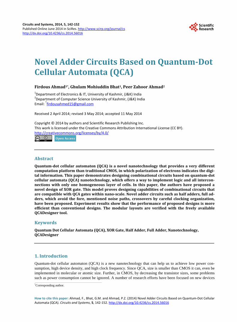
3.2.2. The Second Design Another QCA half-adder is shows in Figure 6(a) using fewer crossovers. The construction of the half-adder is very simple consists of homogeneous layer of cells. The sum is carried out with XOR gate and carry is carried out with AND gate. The proposed half-adder consists of 46 cells, area 0.06 um2 and total circuit latency of 1 clock delays. The simulation result of the proposed half-adder is shown in Figure 6(b).
Table 1. Truth table for conventional half adder.
A B SUM CARRY
0 0 0 0
0 1 1 0
1 0 1 0
1 1 0 1
(a) (b)
Figure 5. (a) QCA based half adder; (b) Simulation results.
F. Ahmad et al.
147
(a) (b)
Figure 6. (a) QCA based half adder (b) Simulation results.
3.3. Proposed QCA Layout of Full Adders Full adders are the main member of computational systems because adders can implement other operations. The proposed XOR design is applied to implement a QCA full adder. QCA implementation of full adders are pre-sented in [30]-[36] has been used for comparison. The comparative study of QCA XOR gate, half adder, and full adder algorithm are given in Table 2.
The logic function of Majority full adder is expressed as: M (A' M (M (B', C, 0), 1), 0), 1)
Sum can be represented in Majority logic as: Sum = M [C'out, Cin, M (A, B, C' in)] (1)
Carry Cout can be represented in Majority logic as: Cout = M (A, B, Cin) (2)
The logical truth table for conventional full adder is shown in Table 2.
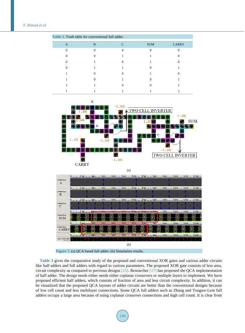
3.3.1. The First Design The QCA layout of the proposed full-adder is shown in Figure 7(a). The proposed full-adder circuit consists of less area and minimum crossovers. The circuit area of the proposed full-adder is 0.15 um2, and circuit complex-ity of 120 cells, using total circuit latency of 2.5 clock delays. The simulation result of the proposed design is shown in Figure 7(b).
3.3.2. The Second Design Figure 8(a) present the other proposed efficient QCA full adder with some inverter and Majority functions, the constructed using to the proposed design consists of no coplanar crossing connections. This QCA layout full adder consists of 69 cells and has 0.08 μm2 occupied area. The simulation result of proposed design is shown in Figure 8(b).
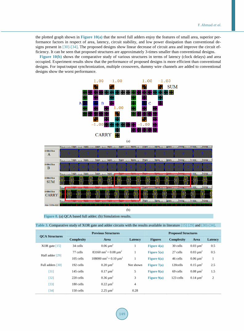
3.3.3. The Third Design Figure 9(a) shows the QCA layout of other proposed full-adder designed basic majority gates and inverters. The simulation result of the proposed full-adder is shown in Figure 9(b). The design consists of basic cells with no crossovers or multilayer’s. The circuit area of the proposed full-adder is 0.14 um2, circuit complexity of 123 cells, and latency of 2 clock delays.
4. Comparison In this section, the proposed QCA XOR gate and its implementations for half adders and full adders have com-pared with conventional designs with regards delay, occupied area, and number of used QCA cells. The effi-ciency and robustness of these adders can verify according to circuit complexity, latency, and the area.
F. Ahmad et al.
148
Table 2. Truth table for conventional full adder.
A B C SUM CARRY
0 0 0 0 0
0 0 1 1 0
0 1 0 1 0
0 1 1 0 1
1 0 0 1 0
1 0 1 0 1
1 1 0 0 1
1 1 1 1 1
(a)
(b)
Figure 7. (a) QCA based full adder; (b) Simulation results.
Table 3 gives the comparative study of the proposed and conventional XOR gates and various adder circuits like half adders and full adders with regard to various parameters. The proposed XOR gate consists of less area, circuit complexity as compared to previous designs [15]. Researcher [17] has proposed the QCA implementation of half adder. The design needs either needs either coplanar crossovers or multiple layers to implement. We have proposed efficient half adders, which consists of fraction of area and less circuit complexity. In addition, it can be visualized that the proposed QCA layouts of adder circuits are better than the conventional designs because of low cell count and less multilayer connections. Some QCA full adders such as Zhang and Tougaw-Lent full adders occupy a large area because of using coplanar crossover connections and high cell count. It is clear from
F. Ahmad et al.
149
the plotted graph shown in Figure 10(a) that the novel full adders enjoy the features of small area, superior per-formance factors in respect of area, latency, circuit stability, and low power dissipation than conventional de-signs present in [30]-[34]. The proposed designs show linear decrease of circuit area and improve the circuit ef-ficiency. It can be seen that proposed structures are approximately 3-times smaller than conventional designs.
Figure 10(b) shows the comparative study of various structures in terms of latency (clock delays) and area occupied. Experiment results show that the performance of proposed designs is more efficient than conventional designs. For input/output synchronization, multiple crossovers, dummy wire channels are added to conventional designs show the worst performance.
(a)
(b)
Figure 8. (a) QCA based full adder; (b) Simulation results. Table 3. Comparative study of XOR gate and adder circuits with the results available in literature [15] [29] and [30]-[34].
QCA Structures Previous Structures Proposed Structures
Complexity Area Latency Figures Complexity Area Latency
XOR gate [15] 34 cells 0.06 µm2 1 Figure 4(a) 30 cells 0.03 µm2 0.5
Half adder [29] 77 cells 83160 nm2 = 0.08 µm2 1 Figure 5(a) 27 cells 0.03 µm2 0.5
105 cells 108000 nm2 = 0.10 µm2 1 Figure 6(a) 46 cells 0.06 µm2 1
Full adders [30] 192 cells 0.20 µm2 Not shown Figure 7(a) 120cells 0.15 µm2 2.5
[31] 145 cells 0.17 µm2 5 Figure 8(a) 69 cells 0.08 µm2 1.5
[32] 220 cells 0.36 µm2 3 Figure 9(a) 123 cells 0.14 µm2 2
[33] 180 cells 0.22 µm2 4
[34] 150 cells 2.25 µm2 0.28

F. Ahmad et al.
150
(a)
(b)
Figure 9. (a) QCA based full adder; (b) Simulation results.
(a) (b)
Figure 10. (a) Efficiency of proposed designs versus conventional designs (b) Area versus latency.

F. Ahmad et al.
151
5. Conclusion The proposed designs are a solution for implementations of QCA based circuits using minimum number of QCA cells, lesser clock delays and reduced area. This paper has demonstrated the design of improved QCA XOR gate and its implementations as novel adder structures, which will be useful as an efficient building block for larger arithmetic units. The simulation results of proposed (half/full) adder circuits have been verified using QCADe-signer. These novel units have been found to have less practical latency and better throughput compared to the best corresponding cases found in the literature, the circuit area is found to be reduced to a fraction of the pre-vious noise rejecting implementations. One aim of this paper is to design simple QCA structures with available basic gates with capable versatility and minimum garbage outputs susceptibility. In addition, results are verified by the truth table.
6. The Future Work This paper has demonstrated the design of improved QCA XOR gate and its implementations as novel adder circuits, which will be useful as an efficient building block for larger arithmetic logic units (ALU) in future. In addition, the proposed designs are a solution for minimum number of QCA cells. The proposed architectural structures can be applied not only to general purpose processing, but to special purpose processing as well. The possibilities of applying the QCA technology to special purpose processing (such as digital signal processors) can also be explored. The QCA layouts and the simulation results are not only demonstrated but also analyzed for a clear understanding and facilitation of the future work. Control signal routing techniques above, work in the immediate future will have an extensive focus on methods for efficient interconnect and routing. Further-more, an efficient and “safe” method of interconnect (i.e. one that avoids as much as possible the design prob-lems) must be considered.
Acknowledgements The authors would like to thank Prof. (Dr.) Rafiq Ahmad Bhat for his literature contribution.
References [1] Compano, R., Molenkamp, L. and Paul, D.J. (1999) Technology Roadmap for Nanoelectronics. Proceeding of the Eu-
ropean Commission IST Programme, Future and Emerging Technologies, Conference 1999. [2] Lent, C.S., Taugaw, P.D., Porod, W. and Berstein, G.H. (1993) Quantum Cellular Automata. Nanotechnology, 4, 49.
http://dx.doi.org/10.1088/0957-4484/4/1/004 [3] Compano, R., Molenkamp, L. and Paul, D.J. (2000) Technology Roadmap for Nanoelectroincs. European Commission
IST Programme, Future and Emerging Technologies. [4] Smith, C.G. (1999) Computation without Current. Science, 284, 274. [5] Lent, C.S., Tougaw, P.D. and Porod, W. (1994) Quantum Cellular Automata: The Physics of Computing with Arrays
of Quantum Dot Molecules. Proceedings of the Workshop on Physics and Computing, Dallas, 17-20 November 1994, 5-13,
[6] Ahmad, P.Z., Ahmad, F. and Khan, H.A. (2014) A New F-Shaped XOR Gate and Its Implementations as Novel Adder Circuits Based Quantum-Dot Cellular Automata (QCA). IOSR Journal of Computer Engineering (IOSR-JCE), 16, 110-117.
[7] Wang, S. and Cai, L. (2007) Novel Exclusive-OR Gate and Full Adder Implementation Using Quantum Cellular Au-tomata. Solid-State Phenomenon, 565-569.
[8] Hänninen, I. and Takala, J. (2007) Robust Adders Based on Quantum-Dot Cellular Automata. IEEE, 1-4244-1027-4. [9] Dehghan, B. (2014) Design Multipurpose Circuits with Minimum Garbage Outputs Using CMVMIN Gate. Chinese
Journal of Engineering, 2014, Article ID: 532121. [10] Vetteth, A. Walus, K. Jullien, G.A. and Dimitrov, V. (2002) Quantum Dot Cellular Automata Carry-Look-Ahead Ad-
der and Barrel Shifter. Proceedings of the IEE Emerging Telecommunication Technologies, Dallas Tex, 2, 1-4. [11] Tougaw, P.D. and Lent, C.S. (1994) Logical Devices Implemented Using Quantum Cellular Automata. Journal of Ap-
plied Physics, American Institute of Physics, 75, 1818-1824. [12] Cho, H. and Swartzlender, E.E. (2007) Adder Designs and Analysis for Quantum-Dot Cellular Automata. IEEE
Transactions on Nanotechnology, 6, 374-383.

F. Ahmad et al.
152
[13] Vetteth, A., Walus, K., Dimitrov, V.S. and Jullien, G.A. (2002) Quantum-Dot Cellular Automata Carry-Look-Ahead Adder and Barrel Shifter. Proceedings of IEEE Emerging Telecommunications Technologies Conference, Dallas, Sep-tember 2002.
[14] Fijany, Toomarian, N., Modarress, K. and Spotnitz, M. (2003) Bit-Serial Adder Based on Quantum Dots. NASA Tech-nical Report, Jan.
[15] Beigh, M.R., Mustafa, M. and Ahmad, F. (2013) Performance Evaluation of Efficient XOR Structures in Quantum-Dot Cellular Automata (QCA). Circuits and Systems, 4, 147-156. http://dx.doi.org/10.4236/cs.2013.42020
[16] Walus, K., Wang, W. and Julliaen, G.A. (2004) Quantum Cellular Automata Adders. Proceedings of the IEEE Confe-rence on Nanotechnology, 3, 461-463.
[17] Walus, K., Schulaf, G. and Julliaen, G.A. (2004) High Level Exploration of Quantum Dot Automata. Proceedings of the IEEE Conference on Nanotechnology, 2, 30-33.
[18] Lent, C.S., Liu, M. and Lu, Y.H. (2006) Bennett Clocking of Quantum-Dot Cellular Automata and the Limits Tobinary Logic Scaling. Nanotechnology, 17, 4240. http://dx.doi.org/10.1088/0957-4484/17/16/040
[19] Liu, W.Q., Srivastava, S., Lu, L., O’Neill, M. and Swartzlander, E.E. (2012) Are QCA Cryptographic Circuits Resis-tant to Power Analysis Attack? IEEE Transactions on Nanotechnology, 11, 1239-1251. http://dx.doi.org/10.1109/TNANO.2012.2222663
[20] Amlani, I., Orlov, A.O., Toth, G., Bernstein, G.H., Lent, C.S. and Snider, G.L. (1999) Digital Logic Gate Using Quan-tum-Dot Cellular Automata. Science, 284, 289-291. http://dx.doi.org/10.1126/science.284.5412.289
[21] Lent, C.S. and Tougaw, P.D. (1997) A Device Architecture for Computing with Quantum Dots. Proceedings of the IEEE, 85, 541-557. http://dx.doi.org/10.1109/5.573740
[22] Smith, C.G. (1999) Computational without Current. Science, 284, 274. [23] Karthigai lakshmi, S. and Athisha, G. (2010) Efficient Design of Logical Structures and Functions Using Nanotech-
nology Based Quantum Dot Cellular Automata Design. International Journal of Computer Applications (0975-8887), 3, 35.
[24] Tougaw, P.D. and Lent, C.S. (1999) Logical Devices Implementation Using Quantum Dot Cellular Automata. Journal of Applied Physics, 75, 1818.
[25] Teja, V.C., Polisetti, S. and Santhosh, K. (2008) QCA Based Multiplexing of 16 Arithmetic & Logical Sub-System a Paradigm for Nano Computing. 3rd Annual IEEE-International Conference on Nano/Micro Engineering Molecular System, Sanya, 6-9 January 2008, 758-763.
[26] Shahidinejad, A. and Selamat, A. (2012) Desien of First Adder/Subtractor Using Quantum-Dot Cellular Automata. Advance Materials Research, 403-408, 3392-3397.
[27] Choi, Myungsu and Choi, Minsu (2008) Scalability of Globally Asynchronous QCA (Quantum-Dot Cellular Automata) Adder Design. Journal of Electronic Testing, 24, 313-320. http://dx.doi.org/10.1007/s10836-007-5052-0
[28] Hanninen, I. and Taka, J. (2008) Arithmetic Design on Quantum-Dot Cellular Automata Nanotechnology. Workshop on Embedded Computer Systems Architectures, Modeling, and Simulation SAMOS, Samos, 21-24 July 2008, 43-52.
[29] Lakshmi, S.K. and Athisha, G. (2011) Design and Analysis of Adders Using Nanotechnology Based Quantum Dot Cellular Automata. Journal of Computer Science, 7, 1072-1079. http://dx.doi.org/10.3844/jcssp.2011.1072.1079
[30] Tougaw, P. and Lent, C. (1994) Logical Devices Implemented Using Quantum Cellular Automata. Journal of Applied Physics, 75, 1818-1825. http://dx.doi.org/10.1063/1.356375
[31] Wang, W., Walus, K. and Jullien, G. (2003) Quantum-Dot Cellular Automata Adders. Proceedings of the 2003 3rd IEEE Conference on Nanotechnology, San Francisco, 12-14 August 2003, 461-464.
[32] Kim, K., Wu, K. and Karri, R. (2007) The Robust QCA Adder Designs Using Composable QCA Building Blocks. IEEE Tractions on CAD Integrated Circuits Systems, 26, 176-183.
[33] Ammar Safavi, A. and Mohammad Mosleh, B. (2013) An Overview of Full Adders in QCA Technology. International Journal of Computer Science & Network Solutions.
[34] Santra, S. and Roy, U. (2014) Design and Implementation of Quantum Cellular Automata Based Novel Adder Circuits. World Academy of Science, Engineering, and Technology. International Journal of Computer, Information Science and Engineering, 8.
[35] Walus, K., Wang, W. and Jullien, G.A. (2004) Majority Logic Reduction for Quantum Cellular Automata. Proceedings of IEEE Conference on Nanotechnology, 3.
[36] Walus, K., Schulaf, G. and Jullien, G.A. (2004) Circuit Design Based on Majority Gates for Application with Quantum Dotcellular Automata. Proceedings of the IEEE Conference on Nanotechnology, 4, 1350-1356.