notes for course ee1.1 circuit analysis 2004-05 topic 5 ...cas.ee.ic.ac.uk/people/dhaigh/ee1.1...
TRANSCRIPT

Notes for course EE1.1 Circuit Analysis 2004-05
TOPIC 5 – THE CAPACITOR, INDUCTOR AND TRANSIENT ANALYSIS
Objectives
• Introduce the capacitor and the inductor
• Consider parallel and series connections of capacitors and inductors
• Consider power and energy for the capacitor and the inductor
• Introduce the switch as a circuit element
• Introduce transient analysis through a computer clock rate example
• Generalise to transient analysis of any 1st order RC or RL circuit
1 THE CAPACITOR
A capacitor is a circuit element that stores charge
It can be made by sandwiching an insulator between two conducting plates in a structure called aparallel-plate capacitor:
The two conducting plates have area Ac and are separated by a dielectric layer of thickness d
As positive charge flows into the capacitor, it begins to accumulate on the plate connected to thatterminal, since it cannot continue to flow through the insulating layer
This accumulation of positive charge attracts negative charge to the opposite plate
This negative charge has to come from somewhere; it can be supplied only by the wire connected tothe opposite plate
This flow of negative charge constitutes an electrical current oriented out of the opposing plate,which is equal in magnitude to the current flowing into the capacitor
From a circuit point of view, it appears that a current is flowing directly through the capacitor

Topic 5 – Capacitor, Inductor and Transient Analysis
2
In order to analyse this capacitor, we define parameters as follows:q Charge on the platesv Voltage between platesAc Area of the platesD Distance between platesε Permittivity of the dielectric between the plates
It can be shown that the charge stored on each of the capacitor plates depends on the voltage acrossthe capacitor in the following way:
�
q = εAc
dv
The relationship between these two quantities is linear;
v
q
0
gradient C
We call the constant of proportionality the capacitance (symbol: C):
�
q = Cv
In general capacitance depends on the geometry and construction of the capacitor
For the parallel-plate capacitor we have been considering, the capacitance is given by:
�
C = εAc
dε is usually expressed as:
ε = εRε0
where εR is the dielectric constant and ε0 = 8.854 × 10⁻¹⁴ F/cm is the permittivity of free space
Since q has units of coulombs, and v is measured in volts, the fundamental unit of capacitance isCoulomb per Volt (C/V) which is called a Farad (abbreviation: F)
Any device capable of storing charge acts as a capacitance, including parasitic capacitance
We can derive the terminal current-voltage characteristics of the device by using the definition ofcurrent:
�
i = dqdt
Differentiating the capacitor q expression results in:
�
dqdt
= ddt
Cv( ) = C dvdt
+ v dCdt

Topic 5 – Capacitor, Inductor and Transient Analysis
3
For a time-invariant capacitor, C is a constant and therefore dC/dt = 0
Hence, the current-voltage relationship for a capacitor is given by:
i = dqdt
= C dvdt
In this equation, i is the current flowing through the capacitor, C is the capacitance, and v is voltageacross the capacitor
This expression tells us that the current through a capacitor is proportional to the time derivative ofthe voltage across it
As long as the voltage is changing, there is current flowing through the capacitor
It follows that there is zero current through a capacitor if the voltage across it is constant, and viceversa
The symbol for a capacitor is as follows:
We have derived an equation for i in terms of v
To obtain an expression for v in terms of i, we can integrate both sides of the equation:
�
v = 1C
i t( )dt + v 0( )∫We have replaced i by i(t) to emphasise that it is a function of time
We have also included an arbitrary constant v(0) (v at time t = 0) which is necessary whenintegrating
v(0) is the voltage stored on the capacitor before we apply the current that is integrated by thecapacitor to produce a change in voltage
Since t is the time at the end of the integration period, it is more correct to plot i as a function of adummy variable x, ie i(x) against x, which has the same graph as i(t) against t
Assuming that we start applying current at t = 0 and are interested in v at time t, we can morecorrectly say:
v = 1C
i x( )dx0
t
∫ + v 0( )
If we apply current at time t1 and are interested in the voltage at time t2, then we have:
v = 1C
i x( )dxt1
t2
∫ + v 1( )
2 THE INDUCTOR
Another circuit element which stores energy is the inductor
Topic 5 – Capacitor, Inductor and Transient Analysis
4
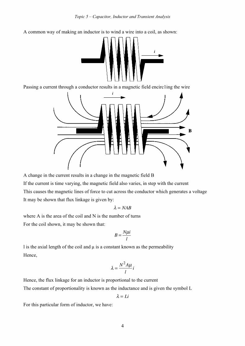
A common way of making an inductor is to wind a wire into a coil, as shown:
Passing a current through a conductor results in a magnetic field encirc1ing the wire
A change in the current results in a change in the magnetic field B
If the current is time varying, the magnetic field also varies, in step with the current
This causes the magnetic lines of force to cut across the conductor which generates a voltage
It may be shown that flux linkage is given by:
λ = NABwhere A is the area of the coil and N is the number of turns
For the coil shown, it may be shown that:
�
B = Nµil
l is the axial length of the coil and µ is a constant known as the permeability
Hence,
λ =N 2Aµl
i
Hence, the flux linkage for an inductor is proportional to the current
The constant of proportionality is known as the inductance and is given the symbol L
λ = LiFor this particular form of inductor, we have:

Topic 5 – Capacitor, Inductor and Transient Analysis
5
L =N 2Aµl
The unit of inductance is the Henry (abbreviation: H), which is equivalent to an ohm-second (Ω-s).
The inductor equation λ = Li corresponds to the equation q = Cv for the capacitor.
The voltage across the inductor terminals is equal to the rate of change of the flux linkage:
v = dλdt
=ddt
Li( ) = L didt
+ i dLdt
Assuming that the inductance L is time-invariant, we have for the inductor:
v = L dtdt
This inductor equation corresponds to the equation i = Cdv/dt for the capacitor.
Note that a constant current flowing through an inductor corresponds to a zero voltage drop
Conversely, if there is zero volts across an inductor, the current through it is constant in time
The circuit symbol for an inductor is as follows:
The reference direction arrow for the current encounters the + sign of the voltage first
We illustrated the phenomenon of inductance using the coil, but it is important to remember thatinductance is an intrinsic property of all conductors, regardless of their shape and it exists whenevercurrent flows; even a straight wire has an inductance, although it is very small.
We have derived an equation for v in terms of i for the inductor
To obtain an expression for i in terms of v, we can integrate both sides of the equation:
i = 1L
v x( )dx0
t
∫ + i 0( )
where x is a dummy variable. If we apply voltage starting at time t1 and are interested in the currentat time t2, then we have:
i = 1L
v x( )dxt1
t2
∫ + i t1( )

Topic 5 – Capacitor, Inductor and Transient Analysis
6
We give a summary of the relationships between i and v for the capacitor and for the inductor:
Expression for i Expression for v
Capacitor
�
i = C dvdt v = 1
Ci x( )dx0
t
∫ + v 0( )
Inductor i = 1L
v x( )dx0
t
∫ + i 0( )
�
v = L didt
The fact that capacitors and inductors can differentiate and integrate voltages and currents makesthem indispensable circuit components, especially for processing signals
Apart from their use as wanted circuit components, it is the case that other types of components,including resistors and transistors, have unwanted parasitic capacitance and inductance which canbe a limiting factor for performance of circuits which operate at high frequencies; hence it is veryimportant to be able to analyze circuits containing capacitors and inductors
2.1 Mechanics analogy
The equations describing electronic components can be regarded as direct mappings of theequations governing mechanics. This leads to an electrical–mechanical analogy:
Electrical Mechanical
Equations
�
i = dqdt
�
v = dsdt
�
v = iR
�
f = vk1
�
v = L didt
�
f = Ma = M dvdt
�
v = 1C
idt∫ f = 1k2
vdt∫ =1k2s
Corresponding parameters
current i ≡ v velocity
charge q ≡ s distance
voltage v ≡ f force
resistance R ≡ k1 damping constant
inductance L ≡ M mass
Capacitance C ≡ k2 inverse spring constant
3 THE SWITCH
The operation of an electrical switch is familiar to all; it passes current when closed, and does notpass current when open
A transistor can acts as a switch

Topic 5 – Capacitor, Inductor and Transient Analysis
7
In fact it is this switching action of a transistor which is exploited in all digital circuits, includingthe computer
The symbol for an ideal switch is as shown
An ideal switch has two states, open and closed
The "switching event" takes place at the time indicated; by convention the switch is drawn in theposition it assumes before the switching event
The switch shown has a switching event at t = t0 and is shown in the open position; thus, byconvention, the switch is open for t < t0, and closed for t> t0
It is also possible to have switches which open at the switching event:
"Open" and "closed" are defined as follows:
• an open switch has i = 0, with no restriction on the voltage across it
• a closed switch has v = 0, with no restriction on the current through it
Upon closer inspection, we see that:
• an open switch can be replaced with an open-circuit or current source of value zero
• a closed switch is identical to a short-circuit or zero-valued voltage source
Ideal switches neither draw nor supply power regardless of the position of the switch
This can be seen from the power relationship p = v × i:
• when the switch is open i = 0
• when the switch is closed v = 0
Suppose we have an ideal switch which closes at t = 0
This means that i = 0 for t < 0 and v = 0 for t > 0
This definition does not strictly define the state of the switch exactly at t = 0

Topic 5 – Capacitor, Inductor and Transient Analysis
8
In order to overcome the ambiguity, we denote as:
V(0–) – voltage at the instant just before switch closure
V(0+) – voltage at the instant just after a switch closure
4 POWER AND ENERGY RELATIONSHIPS FOR R, L AND C
An important aspect of electronic circuits is the rate of energy transfer among the various elements
In this section we develop relationships between circuit variables (such as voltage and current) andthe energy associated with circuit elements
4.1 Power/Energy Relationships for Resistors
Using Ohm's law and the general power formula for a circuit element:
�
p t( ) = v t( )i t( )we find that the power associated with a resistor, pR(t), is:
�
pR t( ) = v t( )i t( ) = i t( )R[ ]i t( ) = Ri2 t( )or, equivalently:
�
pR t( ) = v t( )i t( ) = v t( ) v t( )R
⎡
⎣ ⎢
⎤
⎦ ⎥ =
v 2 t( )R
where v(t) is the voltage drop across the resistor and i(t) is the current through the resistor; we haveassumed that the positive reference arrow for current encounters the + sign of the voltage referencefirst
Note that pR(t) is always a positive quantity; hence resistors always absorb power from theremainder of the circuit (and subsequently convert it into heat); they can never act as a source ofpower
At times it is useful to calculate the total amount of energy absorbed by an element
We can calculate this energy by integrating power over time
For example, the energy absorbed by a resistor from time t = 0 up to time t is given by theexpressions:
ER t( ) = pR t( )dt = Ri2 t( )dt =0
t
∫ R i2 t( )dt0
t
∫0
t
∫
or
ER t( ) = pR t( )dt = v2 t( )R
dt =0
t
∫1R
v2 t( )dt0
t
∫0
t
∫
In either case we see that ER(t) ≥ 0, confirming that resistors always dissipate energy
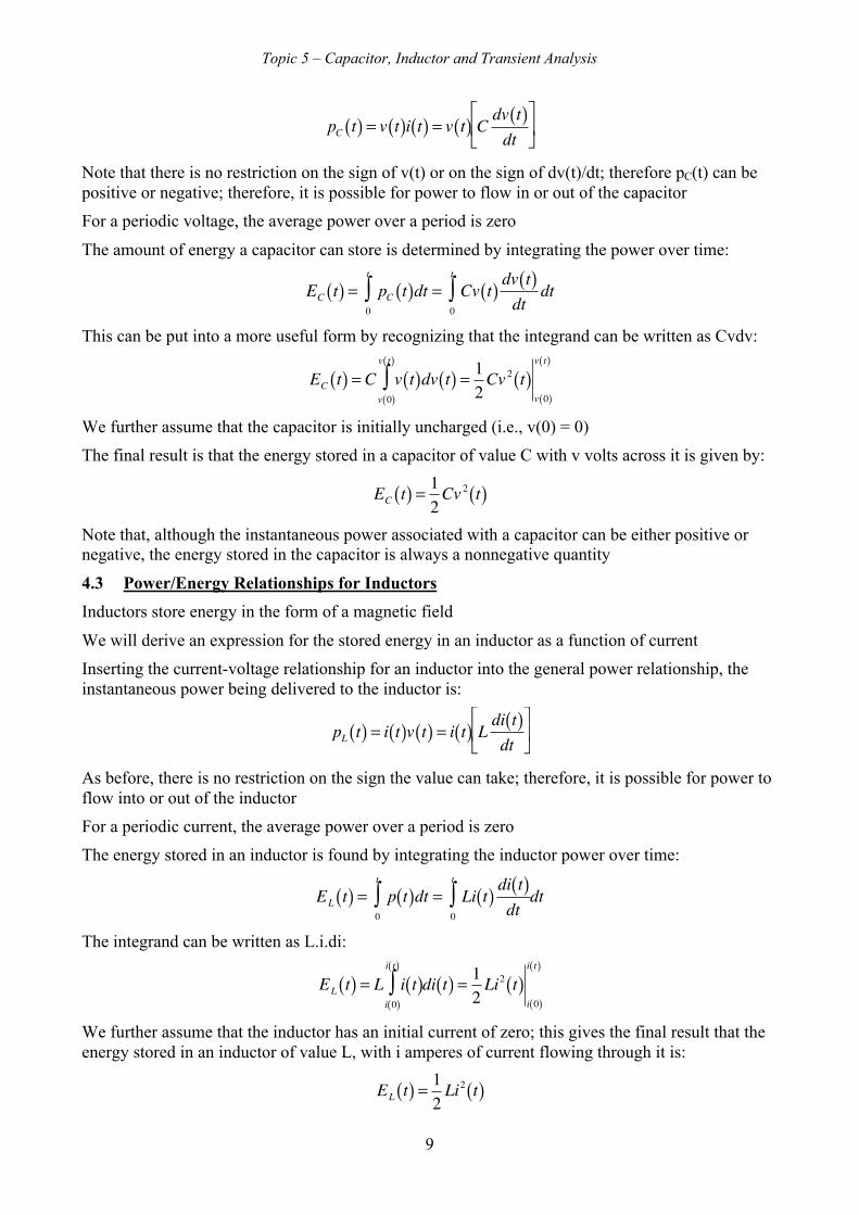
4.2 Power/Energy Relationships for Capacitors
Capacitors are devices which store energy in the form of an electric field, set up by the separation ofcharges
Inserting the current-voltage relationship for a capacitor into the general power relationship, we canexpress the instantaneous power being delivered to the capacitor as:
Topic 5 – Capacitor, Inductor and Transient Analysis
9
�
pC t( ) = v t( )i t( ) = v t( ) C dv t( )dt
⎡
⎣ ⎢
⎤
⎦ ⎥
Note that there is no restriction on the sign of v(t) or on the sign of dv(t)/dt; therefore pC(t) can bepositive or negative; therefore, it is possible for power to flow in or out of the capacitor
For a periodic voltage, the average power over a period is zero
The amount of energy a capacitor can store is determined by integrating the power over time:
�
EC t( ) = pC t( )dt = Cv t( ) dv t( )dt
dt0
t
∫0
t
∫This can be put into a more useful form by recognizing that the integrand can be written as Cvdv:
�
EC t( ) = C v t( )dv t( )v 0( )
v t( )
∫ = 12Cv 2 t( )
v 0( )
v t( )
We further assume that the capacitor is initially uncharged (i.e., v(0) = 0)
The final result is that the energy stored in a capacitor of value C with v volts across it is given by:
�
EC t( ) = 12Cv 2 t( )
Note that, although the instantaneous power associated with a capacitor can be either positive ornegative, the energy stored in the capacitor is always a nonnegative quantity
4.3 Power/Energy Relationships for Inductors
Inductors store energy in the form of a magnetic field
We will derive an expression for the stored energy in an inductor as a function of current
Inserting the current-voltage relationship for an inductor into the general power relationship, theinstantaneous power being delivered to the inductor is:
�
pL t( ) = i t( )v t( ) = i t( ) L di t( )dt
⎡
⎣ ⎢
⎤
⎦ ⎥
As before, there is no restriction on the sign the value can take; therefore, it is possible for power toflow into or out of the inductor
For a periodic current, the average power over a period is zero
The energy stored in an inductor is found by integrating the inductor power over time:
�
EL t( ) = p t( )dt0
t
∫ = Li t( ) di t( )dt0
t
∫ dt
The integrand can be written as L.i.di:
�
EL t( ) = L i t( )i 0( )
i t( )
∫ di t( ) = 12Li2 t( )
i 0( )
i t( )
We further assume that the inductor has an initial current of zero; this gives the final result that theenergy stored in an inductor of value L, with i amperes of current flowing through it is:
�
EL t( ) = 12Li2 t( )

Topic 5 – Capacitor, Inductor and Transient Analysis
10
5 CONTINUITY OF CAPACITOR VOLTAGE AND INDUCTOR CURRENT
5.1 Capacitor voltage continuity
An important function in circuit analysis is the step function:
where the stepped variable could be a voltage or a current
Note that the gradient of the variable at the step is infinite
The branch relationship for a capacitor is:
�
i t( ) = Cdv t( )dt
It follows that the voltage on a capacitor can not be a step function because this would imply aninfinite capacitor current, which is physically impossible
Hence, capacitor voltages must be continuous functions of time, such that the gradient is finite at allvalues of time
The restriction on capacitor voltage in no way prevents discontinuities in capacitor current;capacitor current can change instantaneously and abruptly without restriction
5.2 Inductor current continuity
The branch relationship for an inductor is:
v t( ) = L di t( )dt
Hence, the inductor current must be a continuous function of time and cannot changeinstantaneously
A discontinuity in inductor current would require an infinite amount of voltage which is notpossible in actual circuits
Although inductor currents must be continuous, inductor voltages can change instantaneously andabruptly without restriction
5.3 Forbidden Element Combinations
We showed that the voltage of a capacitor must be a continuous function of time because otherwisethe current would have to be be infinite
Also the current of an inductor must be a continuous function of time because otherwise the voltagewould have to be be infinite
Thus another forbidden combination is a voltage source with a step or pulse waveform connected inparallel with a capacitor
Cvv
t

Topic 5 – Capacitor, Inductor and Transient Analysis
11
Likewise, a forbidden combination is a current source with a step or pulse waveform connected inseries with an inductor
i
t
i L
6 COMBINING REACTIVE CIRCUIT ELEMENTS
6.1 Elements in Series6.1.1 Inductors
Consider the series connection of two inductors shown:
Using KVL and the inductor current-voltage relationship, we can write:
�
v = v1 + v2
= L1di1dt
+ L2di2dt
Since the currents in the two inductors are the same (i1 = i2 = i) it follows that the rates of change ofthe currents are also the same, di1/dt = di2/dt = di/dt:
�
v = L1didt
+ L2didt
= L1 + L2( ) didt
If we replace the two inductors by an equivalent single inductor Leq, we have:
�
v = Leqdidt
Hence,
�
Leq = L1 + L2We can treat the series connection of two inductors as a single equivalent inductance, whose valueis the sum of the inductances
Generalizing, we can replace n inductors in series with an equivalent inductance L equal to the sumof the n individual inductances:
�
Leq = L1 + L2 + ...+ LnIf all n inductors have the same value L:
Leq = nL
Inductors connected in series may be loosely thought of as a single inductor with more turns
Note that for inductors, as for resistors, the equivalent element value is always greater than any ofthe individual element values, assuming positive element values

Topic 5 – Capacitor, Inductor and Transient Analysis
12
6.1.2 Capacitors
Consider the circuit shown:
Applying KVL, we find
v = v1 + v2 + v3
Differentiating this expression:
dvdt
=dv1dt
+dv2dt
+dv3dt
The current-voltage relationship for a capacitor can be expressed as
�
dvdt
= 1Ci
Apply this to each of the derivative terms:
�
dvdt
= iC1
+ iC2
+ iC3
Note that current i is the same for all capacitors
Factoring out i yields:
dvdt
=1C1
+1C2
+1C3
⎛⎝⎜
⎞⎠⎟i
We replace the three series capacitors with an equivalent capacitance Ceq:
This circuit is described by:
�
dvdt
= iCeq
Hence:
�
1Ceq
= 1C1
+ 1C2
+ 1C3
Topic 5 – Capacitor, Inductor and Transient Analysis
13
For capacitors connected in series, the reciprocal of the equivalent capacitance Ceq is given by thesum of the reciprocals of the individual capacitances
Generalising to n capacitors in series:
�
1Ceq
= 1C1
+ 1C2
+ ...+ 1Cn
If all n capacitors have the same value C:
�
1Ceq
= nC
Ceq = Cn
Identical capacitors connected in series may be thought of as a single capacitor where the distancebetween the plates is the sum of the distances for the individual capacitors
Note that the equivalent capacitance of series-connected capacitors is always less than any of theindividual capacitors
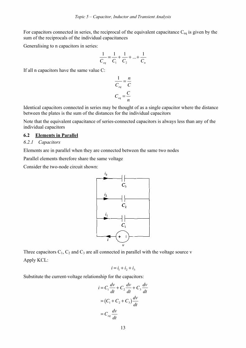
6.2 Elements in Parallel6.2.1 Capacitors
Elements are in parallel when they are connected between the same two nodes
Parallel elements therefore share the same voltage
Consider the two-node circuit shown:
Three capacitors C1, C2 and C3 are all connected in parallel with the voltage source v
Apply KCL:
�
i = i1 + i2 + i3Substitute the current-voltage relationship for the capacitors:
�
i = C1dvdt
+ C2dvdt
+ C3dvdt
= C1 + C2 + C3( ) dvdt
= Ceqdvdt
Topic 5 – Capacitor, Inductor and Transient Analysis
14
Note that since v is the same for all capacitors, dv/dt is also the same; Ceq is a single capacitorequivalent to the three connected in parallel:
Hence:
�
Ceq = C1 + C2 + C3
Ceq is the sum of the individual parallel capacitances
Generalizing for n capacitors in parallel:
�
Ceq = C1 + C2 + ...+ Cn
If all n capacitors have the same value C, then:
Ceq = nC
Capacitors connected in parallel may be loosely thought of as a single capacitor with increased area
Note that the equivalent capacitance of parallel-connected capacitors is always more than any of theindividual capacitors6.2.2 Inductors
It is a straightforward exercise to show that the equivalent inductance of n inductors in parallel isfound using the same rule as for resistors:
�
1Leq
= 1L1
+ 1L2
+ ...+ 1Ln
If all n inductors have the same value L:
1Leq
=nL
Leq =Ln
Note that the equivalent inductance of parallel-connected capacitors is always less than any of theindividual inductors
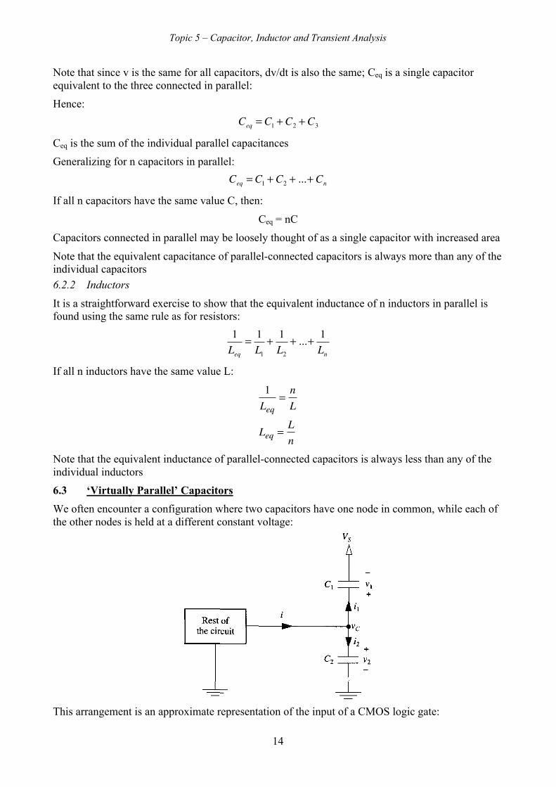
6.3 ‘Virtually Parallel’ Capacitors
We often encounter a configuration where two capacitors have one node in common, while each ofthe other nodes is held at a different constant voltage:
This arrangement is an approximate representation of the input of a CMOS logic gate:
Topic 5 – Capacitor, Inductor and Transient Analysis
15
Applying KCL at node where voltage is vC:
�
i = i1 + i2Substitute current-voltage relationship for each capacitor:
�
i = C1dv1dt
+ C2dv2dt
The two branch voltages v1 and v2, can be related to the node voltages:
�
v1 = vC −VS
v2 = vC − 0 = vChence:
i = C1ddt
vC −VS( ) + C2 ddt vC = C1dvCdt
− C1dVSdt
+ C2dvCdt
Since VS is constant, its derivative is zero:
�
i = C1ddtvC + C2
ddtvC
= C1 + C2( ) dvCdt
Equivalent capacitance Ceq is given by:
�
Ceq = C1 + C2
Hence, the series combination of a DC voltage source (value VS) and a capacitor (C1), is equivalentto the capacitor alone
This is because the current in a capacitor depends on the rate of change of the voltage across it
Since VS is constant with time, the capacitor current is the same as if the capacitor was connected toground instead
The connection of these capacitors is referred to as ‘virtually parallel’
The equivalent capacitance is the same as if the two capacitors were actually in parallel

Topic 5 – Capacitor, Inductor and Transient Analysis
16
6.4 Summary of series and parallel element interconnection rules
Expression for v Expression for i Series Parallel
�
v = Ri
�
i = 1Rv
�
Req = Ri∑
�
1Req
= 1Ri
∑Resistor
v = 1Gi i = Gv
1Geq
=1Gi
∑ Geq = Gi∑
Inductor
�
v = L didt
�
i = 1L
v x( )dxt1
t2
∫ + i t1( )
�
Leq = Li∑
�
1Leq
= 1Li
∑
Voltagesource
�
v =Vs
�
i = arbitrary
�
Veq = Vi∑
�
×
Capacitor
�
v = 1C
i x( )dx0
t
∫ + v 0( )
�
i = C dvdt
�
1Ceq
= 1Ci
∑
�
Ceq = Ci∑
Currentsource
�
v = arbitrary
�
i = Is
�
×
�
Ieq = Ii∑
6.5 DC steady state models for inductors and capacitors
Consider a circuit containing inductors, capacitors and resistors, independent voltage and currentsources and some switches.
When a switch or some switches change state voltages and currents in the circuit will start tochange but they will eventually settle down to the DC steady state values.
The DC steady state solution my be found easily by setting d/dt in the inductor and capacitor v-iand i-v relation to zero:
i-v or v-i relation Relation for t → ∞ Description
Inductor
�
v = L didt v = 0 Short-circuit
Capacitor
�
i = C dvdt i = 0 Open-circuit
Thus we see that the DC steady state model for the inductor is a short-circuit and for the capacitor isan open-circuit.
Hence steady state voltages and currents in a circuit may be obtained by replacing inductors byshort-circuits and capacitors by open-circuits.
We shall use this technique later when we apply transient analysis.
7 DELAY MODEL FOR THE LOGIC INVERTER
7.1 Delays in Logic Circuits
Digital systems, including computers, are mainly composed of logic gates
Topic 5 – Capacitor, Inductor and Transient Analysis
17
Logic gates are circuits that implement logical functions of logic variables
Logical variables take on one of two values, 0 and 1
There is an unavoidable delay between the time at which an input variable changes, from 0 to 1 orfrom 1 to 0, and the time at which the output responds
It is the cumulative effect of these delays which limits the speed of computers and other digitalsystems
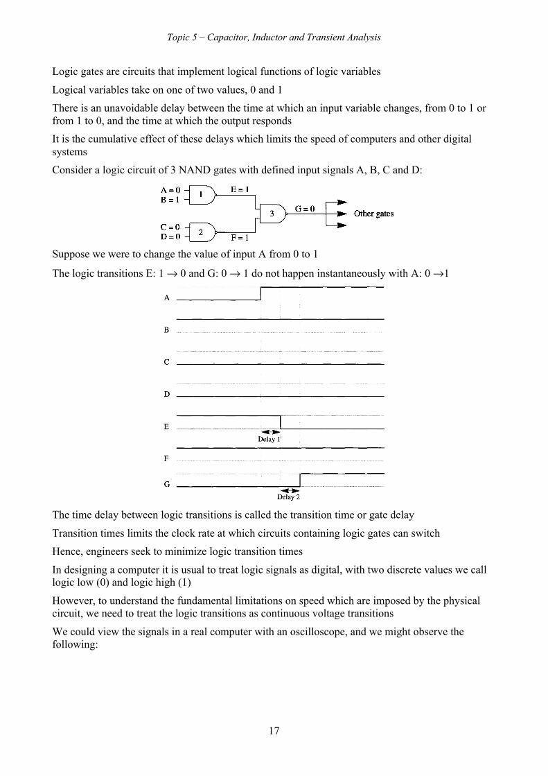
Consider a logic circuit of 3 NAND gates with defined input signals A, B, C and D:
Suppose we were to change the value of input A from 0 to 1
The logic transitions E: 1 → 0 and G: 0 → 1 do not happen instantaneously with A: 0 →1
The time delay between logic transitions is called the transition time or gate delay
Transition times limits the clock rate at which circuits containing logic gates can switch
Hence, engineers seek to minimize logic transition times
In designing a computer it is usual to treat logic signals as digital, with two discrete values we calllogic low (0) and logic high (1)
However, to understand the fundamental limitations on speed which are imposed by the physicalcircuit, we need to treat the logic transitions as continuous voltage transitions
We could view the signals in a real computer with an oscilloscope, and we might observe thefollowing:
Topic 5 – Capacitor, Inductor and Transient Analysis
18
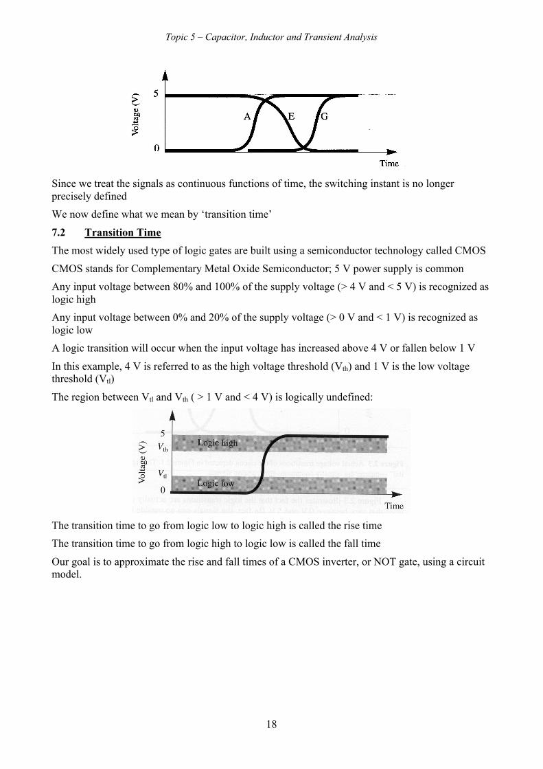
Since we treat the signals as continuous functions of time, the switching instant is no longerprecisely defined
We now define what we mean by ‘transition time’
7.2 Transition Time
The most widely used type of logic gates are built using a semiconductor technology called CMOS
CMOS stands for Complementary Metal Oxide Semiconductor; 5 V power supply is common
Any input voltage between 80% and 100% of the supply voltage (> 4 V and < 5 V) is recognized aslogic high
Any input voltage between 0% and 20% of the supply voltage (> 0 V and < 1 V) is recognized aslogic low
A logic transition will occur when the input voltage has increased above 4 V or fallen below 1 V
In this example, 4 V is referred to as the high voltage threshold (Vth) and 1 V is the low voltagethreshold (Vtl)
The region between Vtl and Vth ( > 1 V and < 4 V) is logically undefined:
The transition time to go from logic low to logic high is called the rise time
The transition time to go from logic high to logic low is called the fall time
Our goal is to approximate the rise and fall times of a CMOS inverter, or NOT gate, using a circuitmodel.
Topic 5 – Capacitor, Inductor and Transient Analysis
19
7.3 Inside the CMOS Inverter
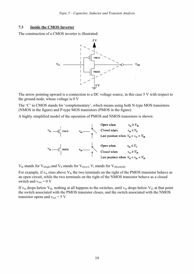
The construction of a CMOS inverter is illustrated:
The arrow pointing upward is a connection to a DC voltage source, in this case 5 V with respect tothe ground node, whose voltage is 0 V
The ‘C’ in CMOS stands for ‘complementary’, which means using both N-type MOS transistors(NMOS in the figure) and P-type MOS transistors (PMOS in the figure)
A highly simplified model of the operation of PMOS and NMOS transistors is shown:
Vth stands for Vt(high) and Vtl stands for Vt(low); Vt stands for V(threshold)
For example, if vin rises above Vth the two terminals on the right of the PMOS transistor behave asan open circuit, while the two terminals on the right of the NMOS transistor behave as a closedswitch and vout = 0 V
If vin drops below Vth, nothing at all happens to the switches, until vin drops below Vtl; at that pointthe switch associated with the PMOS transistor closes, and the switch associated with the NMOStransistor opens and vout = 5 V

Topic 5 – Capacitor, Inductor and Transient Analysis
20
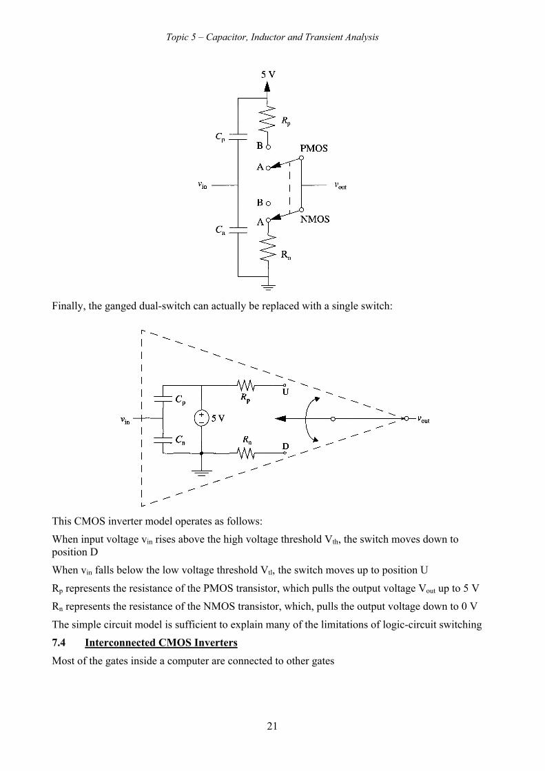
The switch models for the PMOS and NMOS transistors can be combined into a dual-switch modelfor the CMOS inverter:
The two switches move together and simultaneously whenever the input voltage crosses a thresholdvalue
Two key aspects of MOS transistors significantly limit the performance of integrated circuits
MOS transistors do not behave as ideal switches
The path between the two ‘switch contact’ terminals is not a perfect conductor and is bettermodelled by a resistance, typically of the order of 100 Ω
This leads to the dual-resistor-switch model for the CMOS inverter
Separate output resistances Rp and Rn are assumed for the PMOS and NMOS transistors
The other key non-ideal aspect of MOS transistors is input capacitance
We account for this effect by including in the inverter model capacitors Cp and Cn which representthe input capacitances of the PMOS and NMOS transistors, respectively:
Topic 5 – Capacitor, Inductor and Transient Analysis
21
Finally, the ganged dual-switch can actually be replaced with a single switch:
This CMOS inverter model operates as follows:
When input voltage vin rises above the high voltage threshold Vth, the switch moves down toposition D
When vin falls below the low voltage threshold Vtl, the switch moves up to position U
Rp represents the resistance of the PMOS transistor, which pulls the output voltage Vout up to 5 V
Rn represents the resistance of the NMOS transistor, which, pulls the output voltage down to 0 V
The simple circuit model is sufficient to explain many of the limitations of logic-circuit switching
7.4 Interconnected CMOS Inverters
Most of the gates inside a computer are connected to other gates

Topic 5 – Capacitor, Inductor and Transient Analysis
22
Gate delay occurs due to the combination of the output resistance (Rp or Rn) of the first gate and theinput capacitance (Cp and Cn) of the following gate:
The input stage of the first gate is not shown because there is no significant delay between its inputvoltage changing and the switch state changing
Likewise, the output stage of the second gate is not shown because there is no significant delaybetween vc crossing the threshold voltage and its switch state changing
Delay arises only at the interface between gates
When the switch state changes, the capacitor voltage vC can not change instantaneously
The capacitances must be charged or discharged through the resistors tracing out a continuousfunction of time
It is this continuous function of time which determines rise time and fall time which in turndetermine delay and hence maximum clock rate.
The circuit can be analyzed by considering the two possible switching events:
(1) pull-down case when the switch moves down to position D

Topic 5 – Capacitor, Inductor and Transient Analysis
23
(2) pull-up case when the switch moves up to position U
The equivalent circuits to the right are obtained by recognizing that the two capacitors are in the‘virtually parallel’ configuration and may be replaced by a single equivalent capacitor
The two circuits contain one resistor and one capacitor
Circuits that contain only resistors and capacitors, along with sources, are called RC-circuits
Circuits containing only one capacitor, are known as first-order RC-circuits.
8 TRANSIENT ANALYSIS
In circuits containing only resistors and DC voltage and current sources; the currents and voltagesare constant with time
When a circuit contains energy-storage elements such as a capacitance or inductance and switchesthe currents and voltages are functions of time
To determine the current and voltages in our circuit, we will apply Kirchhoff's laws and the v-irelationships for the elements
Consider the pull-down circuit:
Application of KCL at the vc node yields:
�
iR = iCSubstitute the appropriate relations for the branch currents in terms of branch voltages:
�
0 − vCRn
= Cn + Cp( ) dvcdtRearranging:
�
Cn + Cp( ) dvcdt = − vCRn
Consider the pull-up circuit:

Topic 5 – Capacitor, Inductor and Transient Analysis
24
We have:
�
iR = iC
�
5 − vCRp
= Cn + Cp( ) dvcdt
�
Cn + Cp( ) dvcdt = − vCRp
+ 5Rp
To simplify, we let C = Cn + Cp and R = Rn or Rp (as appropriate)
Both the pull-down and pull-up equations can be expressed as the single equation:
�
C dvcdt
= − 1Rvc −Vs( )
Vs = 0 yields the pull-down case and Vs = 5 V yields the pull-up case
Finally, we rearrange the general equation slightly:
�
RC dvcdt
+ vc =Vs
This equation describes the series RC-circuit shown:
The equation we have to solve is a 1st order linear ordinary differential equation
instead of an explicit expression for the variable, vc is expressed in terms of its derivatives(so it is a differential equation).
only the first derivative of the variable vc is present (hence, 1st order);
there are no partial derivatives (therefore, an "ordinary" rather than a "partial" differentialequation);
variable vc occurs as a linear term, not as an argument of another function (hence, linear);
We have taken the case where the switch is closed for both circuits; the equation is valid only for t> 0
9 DIFFERENTIAL EQUATION SOLUTION
The solution involves separating the variables of the differential equation to each side of theequation to allow integration
Since we want to determine vc as a function of time, we denote it by vc(t)
Topic 5 – Capacitor, Inductor and Transient Analysis
25
We put all terms containing variable vc on the left and all terms containing variable t on the right:
�
RCdvc t( )dt
=Vs − vc t( )
RCdvc t( ) = Vs − vc t( )( )dtdvc t( )
Vs − vc t( )= dtRC
dvc t( )vc t( ) −Vs
= − dtRC
Next we integrate both sides of this equation
�
dvc t( )vc t( ) −Vs
∫ = − 1RC
dt∫ + C
C is an arbitrary constant of integration
We need to use the standard result for integration:
�
1xdx∫ = ln x + C
Carrying out the integration:
�
lnvc t( ) −Vs = − 1RC
t + C
Write C as ln(C’) and rearrange:
�
lnvc t( ) −Vs = − 1RC
t + lnC'
lnvc t( ) −Vs − lnC'= − 1RC
t
ln vc t( ) −VsC'
⎛
⎝ ⎜
⎞
⎠ ⎟ = − 1
RCt
Take the exponential of both sides:
�
eln
vc t( )−VsC '
⎛
⎝ ⎜
⎞
⎠ ⎟
= e− 1RC
t
The exponential and natural log are inverse functions:
�
eln x = x
Therefore:
�
vc t( ) −VsC'
=vc t( ) −Vs
C'= e
− 1RC
t
where C’ takes care of the modulus
Hence:

Topic 5 – Capacitor, Inductor and Transient Analysis
26
�
vc t( ) = C'e− 1RC
t+Vs
We now determine the constant of integration C’
Denote the voltage vc(t) at the time when the switch closes (t = 0) by vc(0) = vc0:
�
vc 0( ) = vc0 = C'+VsC'= vc0 −Vs
Hence:
�
vc t( ) = vc0 −Vs( )e− 1RC
t+Vs
Let us do some simple checks on this expression:
1) When t = 0, then vc(t) = vc0, as we specified; this is the initial voltage on the capacitor beforethe switch is closed; we can define it depending on the outcome of the previous switching operation
2) When t → ∞, then vc(t) → Vs, the source voltage
This makes sense because the capacitor can not continue to accumulate charge for ever when thesource is constant with time; once it is charged, the rate of charge flow must fall to zero whichimplies the current is zero; since this current flows also in the resistor, the voltage drop across theresistor must fall to zero; this explains why vc(t) approaches Vs as t → ∞
The exponential term in our equation occurs commonly in transient analysis of circuits and is oftenwritten:
�
e− tRC = e
− tτ
The variable τ is called the time constant
For a series RC-circuit τ = RC
The time constant is a dividing factor on t and its value dictates how rapidly the voltage vc(t) reactsto the change in the switch position
The larger τ is, the slower the response; the smaller τ is, the faster the response
Using τ, the general RC circuit solution may be written:
�
vc t( ) = vc0 −Vs( )e− tτ +Vs
τ is independent of Vs and vc0 and describes the rate of decay of voltage for the RC circuit obtainedwith the switch in its closed state and Vs set to zero, ie Vs is replaced by a short-circuit
The equation:
�
vc t( ) = vc0 −Vs( )e− 1RC
t+Vs
is known as the total response of the circuit

Topic 5 – Capacitor, Inductor and Transient Analysis
27
It consists of two terms, of which one depends on t, and the other is independent of t:
The first term of the general solution is called the transient response:
�
vc0 −Vs( )e− 1RC
t
Just after the switching event at t = 0, the transient response dominates the total response of thecircuit
The transient response of all first order circuits is a decaying exponential function
The transient response decays to zero as t becomes large
This can be seen by examining the limiting value of the transient term as t approaches infinity:
�
limt→∞ vc0 −Vs( )e− 1RC
t⎡
⎣ ⎢ ⎢
⎤
⎦ ⎥ ⎥
= 0
The second part of the solution is called the DC steady-state response
In this example the DC steady-state response is equal to the value of the voltage source Vs
The DC steady-state response is always given by:
�
limt→∞ vc t( )[ ]The notation vc(∞), or just vc∞, is used for DC steady-state capacitor voltage
We now apply the solution to the 1st-order circuit to calculate the switching speed of cascadeddigital inverters
10 CALCULATION OF MAXIMUM COMPUTER CLOCK RATE
10.1 Delays in logic inverters
Using a 1st-order RC model of interconnected inverters, we see that the voltage at the input of thesecond inverter does not change instantaneously when the first inverter switches states
In this section, we examine the waveforms at the input of the second inverter
Consider first the inverter pull-down action
In this case, the second inverter is being pulled down from logic high (5 V) to logic low (0 V):
The input capacitance of the second gate has been given the notation Cin (= Cp + Cn)
We have R = Rn and Vs = 0
Example 2.2
Determine the capacitor voltage as a function of time, given the circuit parameters:
Cin = Cp + Cn = 2 pF

Topic 5 – Capacitor, Inductor and Transient Analysis
28
Rn = 100 Ω
vc0 = 5 V
The time constant is given by:
τ = RnCin = 100 × 2 × 10-12 = 2 × 10-10 = 0.2 ns
From the general solution:
�
vc t( ) = vc0 −Vs( )e− tτ +Vs
For the pull-down switching action:
Vs = 0 V
Hence:
�
vc t( ) = 5 − 0( )e− t2×10−10 + 0
= 5e− t2×10−10
vc(t) is now plotted
The initial transient and the approach to the DC steady state solution can be clearly seen
Note that vc(t) is very close to its DC steady state value around 1 ns, ie after 5 time constants
Now consider the inverter pull-up action
For this case, we have C = Cin = Cp + Cn, R = Rp, Vs = 5 V
The following circuit models the pull-up case of the coupled inverter pair
Topic 5 – Capacitor, Inductor and Transient Analysis
29
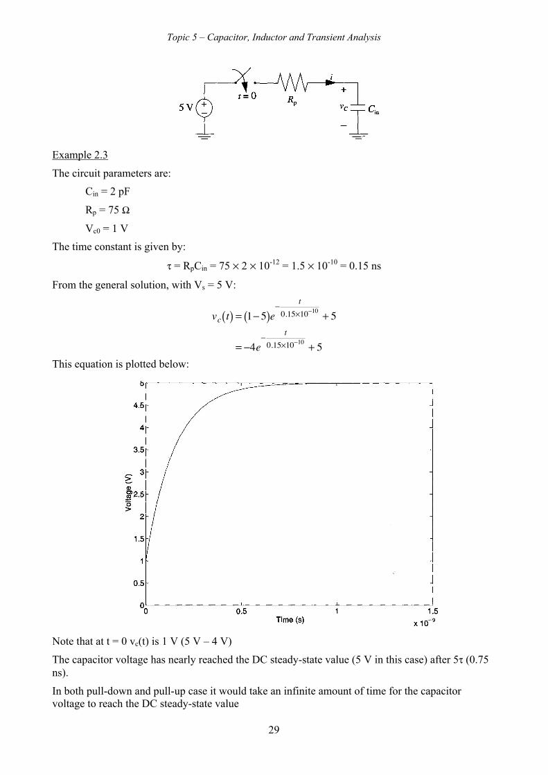
Example 2.3
The circuit parameters are:
Cin = 2 pF
Rp = 75 Ω
Vc0 = 1 V
The time constant is given by:
τ = RpCin = 75 × 2 × 10-12 = 1.5 × 10-10 = 0.15 ns
From the general solution, with Vs = 5 V:
�
vc t( ) = 1− 5( )e− t0.15×10−10 + 5
= −4e− t0.15×10−10 + 5
This equation is plotted below:
Note that at t = 0 vc(t) is 1 V (5 V – 4 V)
The capacitor voltage has nearly reached the DC steady-state value (5 V in this case) after 5τ (0.75ns).
In both pull-down and pull-up case it would take an infinite amount of time for the capacitorvoltage to reach the DC steady-state value

Topic 5 – Capacitor, Inductor and Transient Analysis
30
We observe, though, that there is little change after a period of approximately 5τ
However, it is not necessary for the voltage to completely reach the steady-state value before thenext inverter switches
The important parameters involved in gate switching are the threshold voltages: Vth (for the pull-up)and Vtl (for the pull-down)
The gate delay is defined by the time it takes for the voltage to reach the appropriate thresholdvoltage, which is typically much shorter than 5τ in a well-designed system
For example, if Vth = 4 V, the second inverter would switch well before 2τ, ie 0.3 ns
10.2 Maximum Inverter-Pair Switching Speed
We can now calculate the maximum frequency at which a pair of cascaded CMOS inverter gatescan be switched
We assume that the switch inside the driving inverter changes state at frequency f
When frequency f is too high, the next inverter fails to recognise that a changed state has beenreached and fails to switch
Our task is to determine the frequency f = fmax at which this occurs
The voltage at the output of the switch inside the driving inverter (Vs in our equivalent circuit) canbe assumed to take the form of a square wave, which is typical of signals generated by clock circuitryin computers
We assume that the clock signal is symmetric, spending an equal amount of time at logic high andlogic low
The ratio of time at the high level to the period expressed as a percentage is called the duty cycle
The symmetric clock signals we will deal with have a 50% duty cycle

Topic 5 – Capacitor, Inductor and Transient Analysis
31
In order to calculate the maximum switching frequency, we first assume that the initial conditionsfor the capacitor voltage (vc0) are either 0 V (logic low) or 5 V (logic high)
We will assume the following:
Vth = 3.7 V (therefore vc is logic high if 3.7 ≤ vc ≤ 5)
Vtl = 1 V (therefore vc is logic low if 0 ≤ vc ≤ 1)
Rn = 100 Ω
Rp = 150 Ω
Cin = Cn + Cp = 1 pF
We now calculate the transition time for the input voltage of the second inverter to go from 0 V toVth (pull-up case) and the transition time from 5 V to Vtl (pull-down case)
Once this voltage has reached a threshold value, the load inverter will switch, resulting in a forwardpropagation of the logic signal
If the voltage was to switch before threshold had been reached, the logic signal would not triggerthe next inverter
10.3 Pull-Up Transition Time
The circuit model and the voltage across the capacitor are as follows:
We determine the transition time tl, defined as the time required for vc rise from 0 V to Vth
vc is given by:

Topic 5 – Capacitor, Inductor and Transient Analysis
32
�
vc t( ) = vc0 −Vs( )e− tτ +Vs
Substituting the given values yields:
�
vc t( ) = 0 − 5( )et
1.5×102×10−12 + 5
= 5 − 5e− t1.5×10−10
At time t = tl the capacitor voltage is at the logic high threshold ∴ vc(t1) = Vth = 3.7
�
3.7 = 5 − 5e− t11.5×10−10
Solving for t1:
�
−1.3 = −5e− t11.5×10−10
1.35
= e− t11.5×10−10
ln 1.35
⎛ ⎝ ⎜
⎞ ⎠ ⎟ = − t1
1.5 ×10⁻¹⁰
t1 = −1.5 ×10⁻¹⁰ × ln 1.35
⎛ ⎝ ⎜
⎞ ⎠ ⎟ = 0.202 ×10−9 = 0.202ns
It requires 0.202 ns for the inverter to switch from 0 V to the logic high threshold of 3.7 V
10.4 Pull-Down Transition Time
The circuit model and the voltage across the capacitor at the input of the second inverter are asfollows:
We determine the transition time t2, for vc to fall from 5 V to Vtl
From the general solution, we have:
�
vc t( ) = 5 − 0( )et
102×10−12 + 0 = 5e− t10−10

Topic 5 – Capacitor, Inductor and Transient Analysis
33
At time t = t2 the capacitor voltage is at the logic low threshold ∴ vc(t2) = Vtl = 1
�
1= 5e− t210−10
Solving for t2:
�
15
= e− t210−10
ln 15⎛ ⎝ ⎜
⎞ ⎠ ⎟ = − t2
10−10
t2 = −10−10 × ln 15
⎛ ⎝ ⎜
⎞ ⎠ ⎟ = 0.161×10−9 = 0.161ns
It requires 0.161 ns for the inverter to switch from 5 V to the logic low threshold of 1 V
10.5 Maximum clock rate
The pull-up transition time, 0.202 ns, is greater than the pull-down transition time of 0.161 ns
In designing a digital system we should allow for the worst case and make the clock period at leasttwice the longer delay:
T0 = 2t1 = 2 × 0.202 ns = 0.404 ns
The clock frequency is equal to the reciprocal of the period; this determines the maximum clockfrequency:
�
fmax = 10.404 ×10−9
= 2.48 ×109 = 2.48GHz
This calculated maximum clock frequency is only an approximation of the coupled inverter pair'strue operating limit as we have used many simplifying assumptions
These include a linear circuit model for the inverters and the assumption that the critical vc
transitions started from initial conditions of 0 V and 5 V
In practice, the initial condition voltage on the capacitor would be the result of the previoustransition
As a result, the following waveforms are more likely:
On the positive transition, vc passes the Vth by a reasonable margin reaching a maximum of vh
On the negative transition, vc passes the Vtl by a reasonable margin reaching a minimum of vl

Topic 5 – Capacitor, Inductor and Transient Analysis
34
The equations we have developed can be applied to this case also and typically lead to maximumclock rates about 10 % higher than figures produced under the previous assumptions
11 GENERAL RESULT FOR 1ST ORDER RC CIRCUIT
The general pull-up/pull-down circuit is:
The general equation for the capacitor voltage we have derived is as follows::
�
vc t( ) = vc0 −Vs( )e− tτ +Vs
where vc0 is the initial condition voltage on the capacitor at t = 0
Since for t → ∞ , vc(t) → Vs, the equation may be written
�
vc t( ) = vc0 − vc∞( )e− tτ + vc∞
= vc∞ − vc∞ − vc0( )e− tτ
= Final value – (Range)× e− tτ
where vc(t → ∞) is abbreviated to vc∞:
When t = 0, e-t/τ = 1 and vc(t) = vc0
When t → ∞ , e-t/τ → 0 and vc(t) → vc∞
The equation may be written in the alternative form:
�
vc t( ) = vc0 + vc∞ − vc0( ) 1− e− tτ
⎛
⎝ ⎜ ⎜
⎞
⎠ ⎟ ⎟
= Initial value +(Range)× 1− e− tτ
⎛
⎝ ⎜ ⎜
⎞
⎠ ⎟ ⎟
When t = 0, 1 – e-t/τ = 0 and vc(t) = vc0
When t → ∞ , 1 – e-t/τ → 1 and vc(t) → vc∞
We can find the slope of vc(t) by differentiating:
�
vc t( ) = vc∞ − vc∞ − vc0( )e− tτ
dvc t( )dt
= vc∞ − vc0τ
e− tτ
The initial slope is obtained by setting t = 0:
Topic 5 – Capacitor, Inductor and Transient Analysis
35
�
dvc t( )dt t=0
= vc∞ − vc0τ
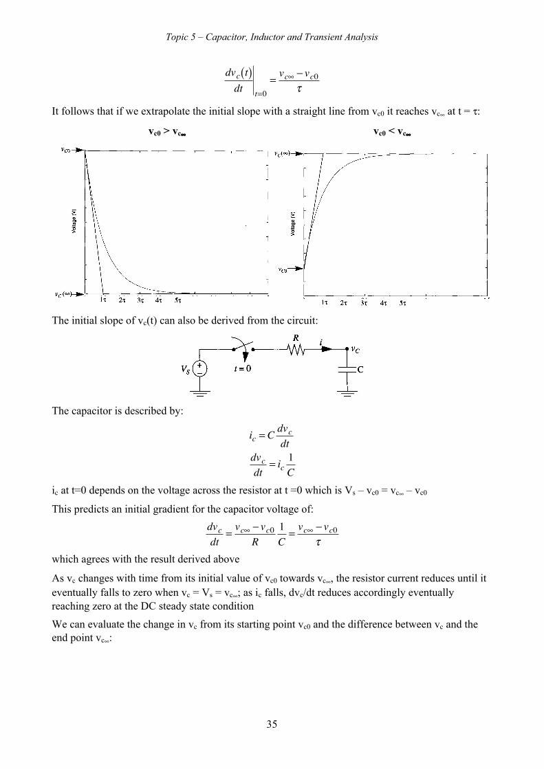
It follows that if we extrapolate the initial slope with a straight line from vc0 it reaches vc∞ at t = τ:
vc0 > vc∞ vc0 < vc∞
The initial slope of vc(t) can also be derived from the circuit:
The capacitor is described by:
�
ic = C dvcdt
dvcdt
= ic1C
ic at t=0 depends on the voltage across the resistor at t =0 which is Vs – vc0 = vc∞ – vc0
This predicts an initial gradient for the capacitor voltage of:
�
dvcdt
= vc∞ − vc0R
1C
= vc∞ − vc0τ
which agrees with the result derived above
As vc changes with time from its initial value of vc0 towards vc∞, the resistor current reduces until iteventually falls to zero when vc = Vs = vc∞; as ic falls, dvc/dt reduces accordingly eventuallyreaching zero at the DC steady state condition
We can evaluate the change in vc from its starting point vc0 and the difference between vc and theend point vc∞:
Topic 5 – Capacitor, Inductor and Transient Analysis
36
�
vc t( ) − vc0 = 1− e− tτ
⎛
⎝ ⎜ ⎜
⎞
⎠ ⎟ ⎟ vc∞ − vc0( )
vc∞ − vc t( ) = e− tτ vc∞ − vc0( )
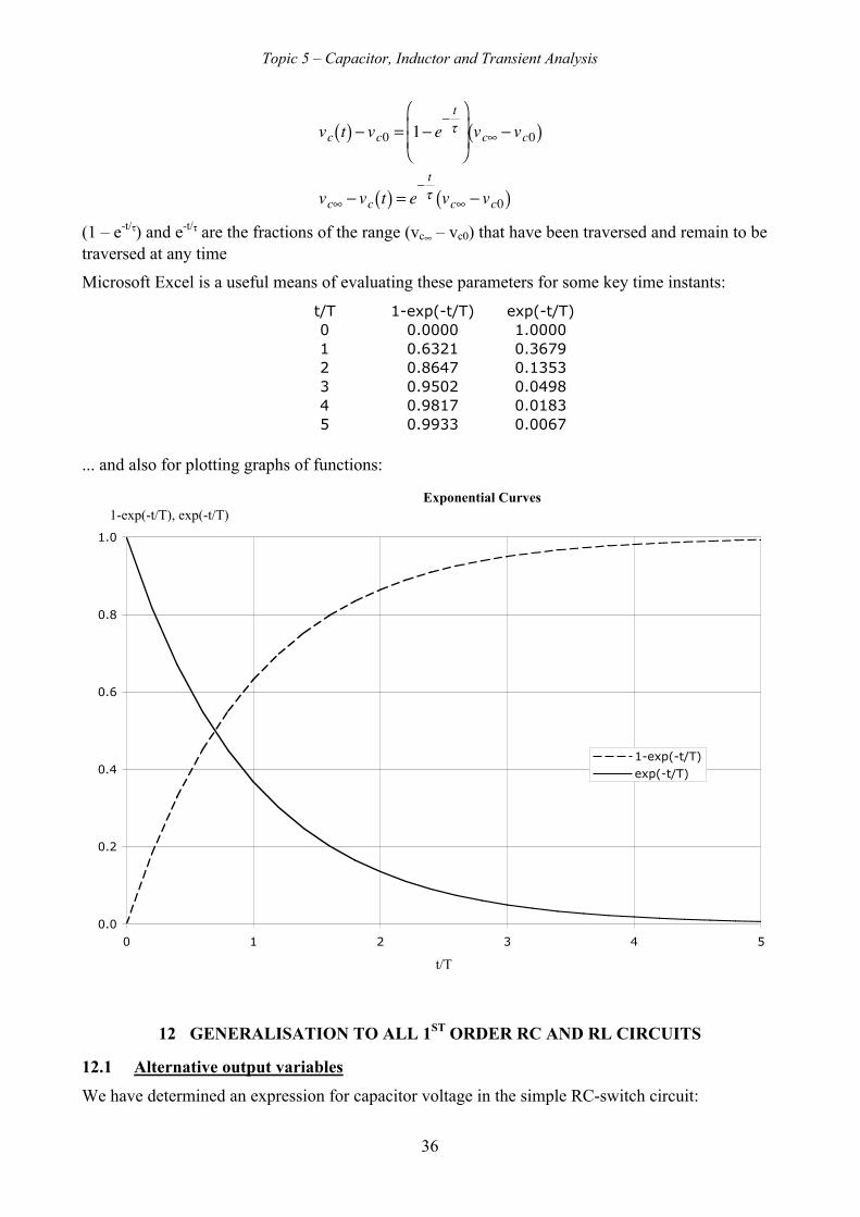
(1 – e-t/τ) and e-t/τ are the fractions of the range (vc∞ – vc0) that have been traversed and remain to betraversed at any time
Microsoft Excel is a useful means of evaluating these parameters for some key time instants:
t/T 1-exp(-t/T) exp(-t/T)0 0.0000 1.00001 0.6321 0.36792 0.8647 0.13533 0.9502 0.04984 0.9817 0.01835 0.9933 0.0067
... and also for plotting graphs of functions:
Exponential Curves
0.0
0.2
0.4
0.6
0.8
1.0
0 1 2 3 4 5
t/T
1-exp(-t/T), exp(-t/T)
1-exp(-t/T)exp(-t/T)
12 GENERALISATION TO ALL 1ST ORDER RC AND RL CIRCUITS
12.1 Alternative output variables
We have determined an expression for capacitor voltage in the simple RC-switch circuit:
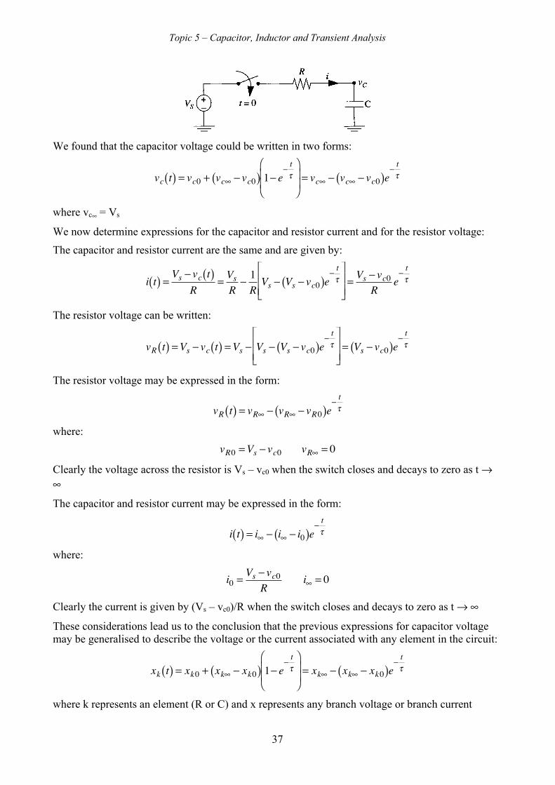
Topic 5 – Capacitor, Inductor and Transient Analysis
37
We found that the capacitor voltage could be written in two forms:
�
vc t( ) = vc0 + vc∞ − vc0( ) 1− e− tτ
⎛
⎝ ⎜ ⎜
⎞
⎠ ⎟ ⎟ = vc∞ − vc∞ − vc0( )e
− tτ
where vc∞ = Vs
We now determine expressions for the capacitor and resistor current and for the resistor voltage:
The capacitor and resistor current are the same and are given by:
�
i t( ) =Vs − vc t( )
R= VsR
− 1RVs − Vs − vc0( )e
− tτ
⎡
⎣ ⎢ ⎢
⎤
⎦ ⎥ ⎥
= Vs − vc0R
e− tτ
The resistor voltage can be written:
�
vR t( ) =Vs − vc t( ) =Vs − Vs − Vs − vc0( )e− tτ
⎡
⎣ ⎢ ⎢
⎤
⎦ ⎥ ⎥
= Vs − vc0( )e− tτ
The resistor voltage may be expressed in the form:
�
vR t( ) = vR∞ − vR∞ − vR0( )e− tτ
where:
�
vR0 =Vs − vc0 vR∞ = 0
Clearly the voltage across the resistor is Vs – vc0 when the switch closes and decays to zero as t →∞
The capacitor and resistor current may be expressed in the form:
�
i t( ) = i∞ − i∞ − i0( )e− tτ
where:
�
i0 = Vs − vc0R
i∞ = 0
Clearly the current is given by (Vs – vc0)/R when the switch closes and decays to zero as t → ∞
These considerations lead us to the conclusion that the previous expressions for capacitor voltagemay be generalised to describe the voltage or the current associated with any element in the circuit:
�
xk t( ) = xk0 + xk∞ − xk0( ) 1− e− tτ
⎛
⎝ ⎜ ⎜
⎞
⎠ ⎟ ⎟ = xk∞ − xk∞ − xk0( )e
− tτ
where k represents an element (R or C) and x represents any branch voltage or branch current
Topic 5 – Capacitor, Inductor and Transient Analysis
38
Once k and x are chosen, it is only necessary to determine by inspection the values of xk at t = 0+
and for t → ∞ and the time constant τ in order to write down the expression for xk(t)
If the resistor and capacitor in the circuit are interchanged, the voltages and currents associated withthe elements do not change
Infact, this approach is valid for any RC circuit topology with a single time constant
It also applies to any RL circuit with a single time constant; in this case, the initial condition wouldbe an inductor current rather than a capacitor voltage and the time constant is given by τ = L/R
We now consider the case of circuits where there is more that one resistor or capacitor
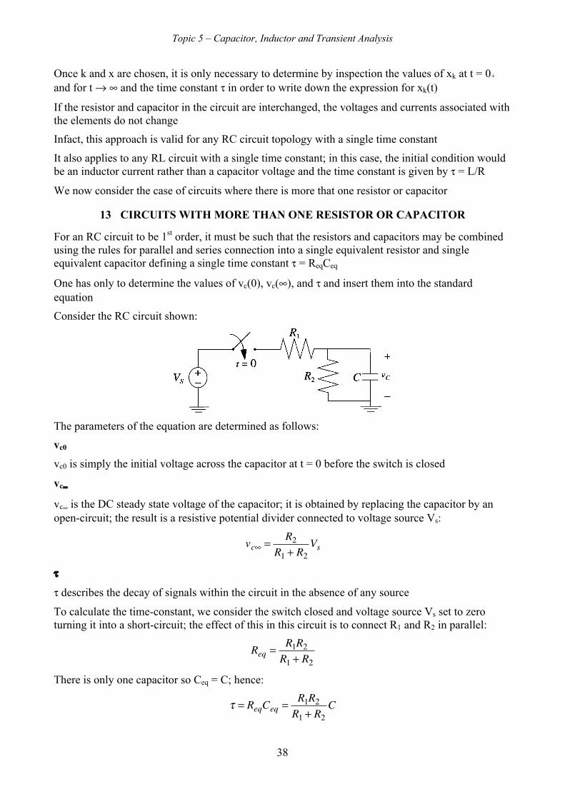
13 CIRCUITS WITH MORE THAN ONE RESISTOR OR CAPACITOR
For an RC circuit to be 1st order, it must be such that the resistors and capacitors may be combinedusing the rules for parallel and series connection into a single equivalent resistor and singleequivalent capacitor defining a single time constant τ = ReqCeq
One has only to determine the values of vc(0), vc(∞), and τ and insert them into the standardequation
Consider the RC circuit shown:
The parameters of the equation are determined as follows:
vc0
vc0 is simply the initial voltage across the capacitor at t = 0 before the switch is closed
vc∞
vc∞ is the DC steady state voltage of the capacitor; it is obtained by replacing the capacitor by anopen-circuit; the result is a resistive potential divider connected to voltage source Vs:
�
vc∞ = R2R1 + R2
Vs
τ
τ describes the decay of signals within the circuit in the absence of any source
To calculate the time-constant, we consider the switch closed and voltage source Vs set to zeroturning it into a short-circuit; the effect of this in this circuit is to connect R1 and R2 in parallel:
�
Req = R1R2R1 + R2
There is only one capacitor so Ceq = C; hence:
�
τ = ReqCeq = R1R2R1 + R2
C
Topic 5 – Capacitor, Inductor and Transient Analysis
39
The capacitor voltage in this circuit is given by substituting these expressions into the generalequation:
vc t( ) = R2R2 + R1
Vs −R2
R2 + R1Vs − vc0
⎛⎝⎜
⎞⎠⎟e−t R1+R2( )R1R2C
If there is more than one switch in the circuit and they close at different times, then the method isused to find the capacitor voltage when the second switch changes state; this can be used as theinitial condition for the next switching action and so on
13.1 Worked examples
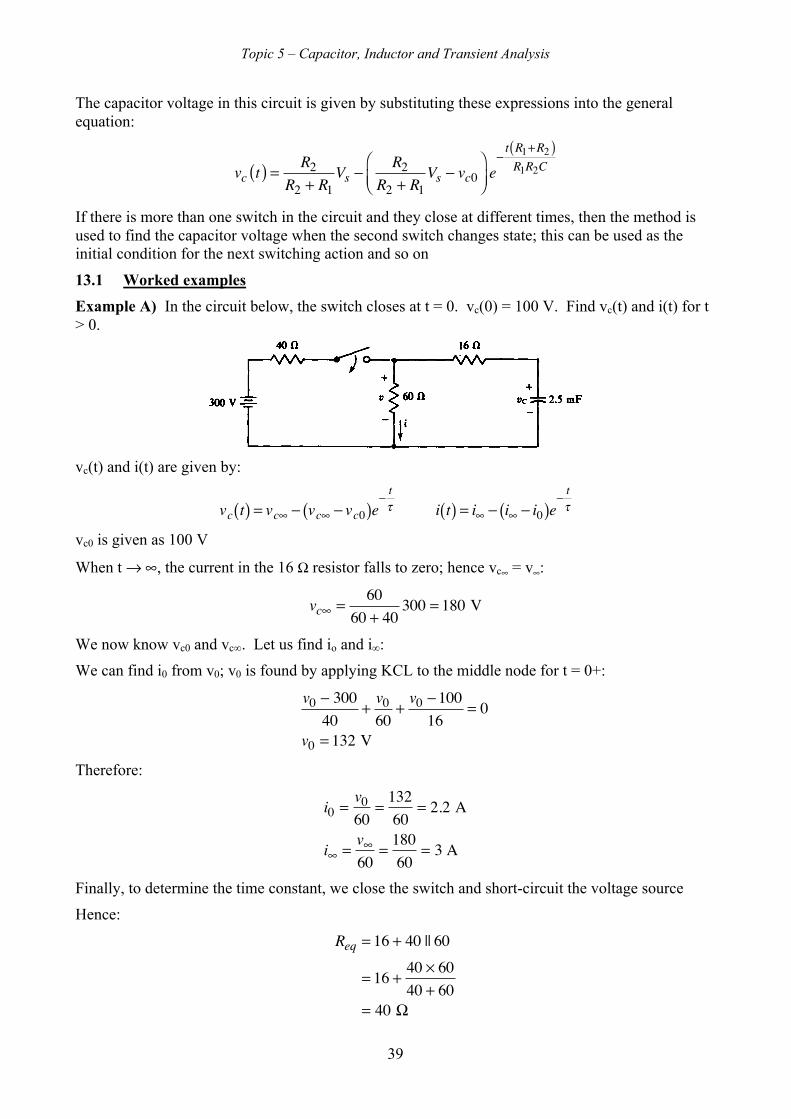
Example A) In the circuit below, the switch closes at t = 0. vc(0) = 100 V. Find vc(t) and i(t) for t> 0.
vc(t) and i(t) are given by:
�
vc t( ) = vc∞ − vc∞ − vc0( )e− tτ i t( ) = i∞ − i∞ − i0( )e
− tτ
vc0 is given as 100 V
When t → ∞, the current in the 16 Ω resistor falls to zero; hence vc∞ = v∞:
vc∞ =60
60 + 40300 = 180 V
We now know vc0 and vc∞. Let us find io and i∞:
We can find i0 from v0; v0 is found by applying KCL to the middle node for t = 0+:
v0 − 30040
+v060
+v0 −100
16= 0
v0 = 132 V
Therefore:
i0 =v060
=13260
= 2.2 A
i∞ =v∞60
=18060
= 3 A
Finally, to determine the time constant, we close the switch and short-circuit the voltage source
Hence:
Req = 16 + 40 || 60
= 16 +40 × 6040 + 60
= 40 Ω
Topic 5 – Capacitor, Inductor and Transient Analysis
40
�
τ = CReq= 2.5 ×10−3 × 40= 0.1s
Hence, vc(t) and i(t) are given by the following:
�
vc t( ) = 180 − 180 −100( )e−10t = 180 − 80e−10t
i t( ) = 3− 3− 2.2( )e−10t = 3− 0.8e−10t
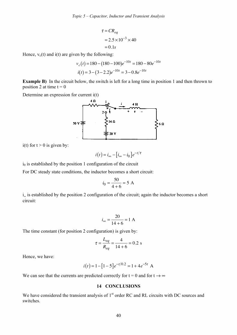
Example B) In the circuit below, the switch is left for a long time in position 1 and then thrown toposition 2 at time t = 0
Determine an expression for current i(t)
i(t) for t > 0 is given by:
i t( ) = i∞ − i∞ − i0[ ]e−t τi0 is established by the position 1 configuration of the circuit
For DC steady state conditions, the inductor becomes a short circuit:
i0 =50
4 + 6= 5 A
i∞ is established by the position 2 configuration of the circuit; again the inductor becomes a shortcircuit:
i∞ =20
14 + 6= 1 A
The time constant (for position 2 configuration) is given by:
τ =LeqReq
=4
14 + 6= 0.2 s
Hence, we have:
i t( ) = 1− 1− 5[ ]e−t 0.2 = 1+ 4e−5t A
We can see that the currents are predicted correctly for t = 0 and for t → ∞
14 CONCLUSIONS
We have considered the transient analysis of 1st order RC and RL circuits with DC sources andswitches.

Topic 5 – Capacitor, Inductor and Transient Analysis
41
All voltages and currents in such circuits are exponential functions of time governed by RC or L/Rtime constants.
The coefficients in the equations depend on the initial and final values of a voltage or current.
Next we consider analysis of circuits with voltages and currents which are sinusoidal functions oftime.