not ice · o+f -the-shelf i n st rument a t i on was not available. . ... bridge expansion joints,...
TRANSCRIPT

NOT I C E
THE UNITED STATES GOVERNMENT DOES NOT ENDORSE PRODUCTS OR
SOLELY BECAUSE THEY ARE CUNSIDERED ESSENTIAL TO THE OBJECT OF T H I S TECHNICAL MANUCIL.
MANUFACTURERS. TRADE OR MANUFACTURERS’ NAMES APPEAR HEREIN
D I SCLA I MER STATEMENT
THE CONTENTS OF T H I S REPORT REFLECT THE VIEWS OF THE AUTHOR WHO I S RESPONSIBLE FOR THE FACTS AND THE ACCURACY OF THE DATA PRESENTED HEREIN. THE CONTENTS DO NOT NECESSARILY REFLECT THE O F F I C I A L VIEWS OR POLIC IES OF THE NEW JERSEY DEPARTMENT OF TRANSPORTATION OR THE UNITED STATES DEPARTMENT OF TRANSPORTATION, FEDERAL HIGHWAY ADMINISTRATION. T H I S REPORT DOES NOT CONSTITUTE A STANDARD, SPECIFICATION OR REGULATION.
COPYRIGHT NOTICE
COPYRIGHT (C) 1985 B Y WALLACE C. RICHARDSON. THE NEW JERSEY DEPARTMENT OF TRANSPORTATION AND THE UNITED STATES DEPARTMENT OF TRANSPORTATION, HOWEVER, ARE GRANTED “ROYALTY FREE NON EXCLUSIVE AND IRREVOCABLE RIGHTS TO REPRODUCE, PUBLISH, OR OTHERWISE US€ AND TO AUTHORIZE OTHERS TO USE THE WORK FOR DOVERMENT PURPOSES.”
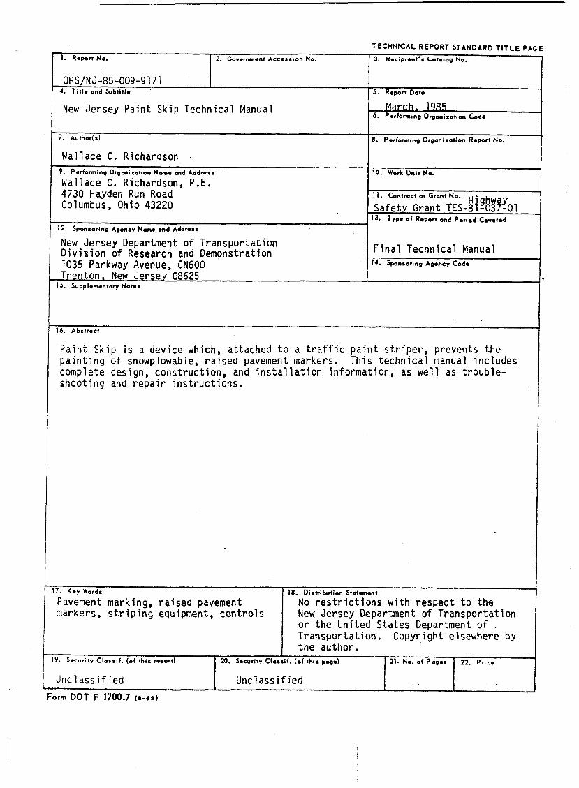
1. Report No.
OHS/NJ-85-009-9171
New Jersey Paint Skip Technical Manual
2. Govemmont Accession No. 3. Recipient's Catalog No.
March. 1985 6. Performing Organization Code
4. Title m d Subtitle '
I 18. Performing Orgonixation Report NO. 7. Aurhor(s) I
5. Report Date
Wallace C. Richardson . I 1 9. Porforming Organization Nomo md Address
Wallace C. Richardson, P.E.
Columbus, Ohio 43220 4730 Hayden Run Road
12. Sponsoring Agency N a e ond Addrers
10. Work Unit No.
H'gh Y 11. Contract or Grant No.
Safety Grant TES-8l-0!!?-01 13. TYPO of Report and Period Covered
New Jersey Department of Transportation Division of Research and Demonstration 1035 Parkway Avenue, CN600
7. K e y Words
Pavement marking, raised pavement markers, striping equipment, controls
Final Technical Manual 14. Sponsoring Agency Cod.
18. Distribution Statwarn?
No restrictions with respect to the New Jersey Department of Transportation or the United States Department of . Transportation. Copyright elsewhere by the author.
Trenton. New Jersey- 08625 I IS. Supplementary Notes
9- Security Classif. (of thls r m p w r )
Unclassified
16. Abrtroct
20. Security Classif. (of th is pogo) 21- No. of Pages 22. Prtce
Unclassified
Paint Skip i s a device which, attached to a traffic paint striper, prevents the painting of snowplowable, raised pavement markers. This technical manual includes complete design, construction, and installation information, as well as trouble- shooting and repair instructions.

TABLE O F CONTENTS
PAGE
1. I NTRODUCT ION New Jersey Ohio
2.THEORY OF OPERATION General Host Paint System P s i nt-Sk i p Ci r cui t Det ai 1 s
3. REFERENCES
4. CONSTRUCT I ON
5. INSTALLATION
6.0PERATION AND MAINTENANCE Front Panel Back Panel Adjustment Maintenance
7.CHECKOUT FIND TROUBLESHOOTING Equi pment Needed Bench Checkout Test Fai 1 ure Procedures Voltage and Waveform Table Troubleshooting Guide
APPENDICES
A. FIWRES 1.Paint System Operation 2. Pai nt-Ski p Funct i onal B1 ac k Di agram 3.Paint-Skip Schematic Diagram 4.Front Panel Drill Template S.Rear Panel Drill Template 6.Bottom Panel Drill Template 7.Front Panel Lettering 8.Rear Panel Lettering 9.Chasrir Parts Layout 10.Parts Placrmcant-PC Component Side 1l.Parts Placement-Foil Side 12.Antenna Construction
1 2
5 5 & 9
13
14
20
23 24 24 26
27 28 30 31 33
36 37 38 39 40 41 42 43 44 425 46 47

A. FIGURES (Cont. 1 13. Asrembl y Drawi ng 14.Printed Circuit
E.PARTS LIST AND SOURCES O F SUPPLY Parts Lirt and Recommended Spare Parts Sources of Supply
C. WAVEFORM PICTORIALS Waveform 1 Waveform 2 Waveform 3 Wavdorm 4 Waveform 5 Waveform 6 Waveform 7 Waveform 8 Waveform 9 Waveform 10
D.SEMIC0NDUCTOR CCITALOG PAGES Q2-Trrnsi stor, PNP Power Darl i nqton Z1-Integrated Circuit, Phase Lock Loop Z2-Integrated Circuit, Operational Amplifier Z3-Integrated Ci rcui t, Dual Timer Z4-Integrated Circuit, Hex Inverting Buffer ZS-Integrated Circuit, Voltage Regulator
48 49
51 56
60 60 61 61 62 62 63 63 64 64
66 71 76 81 90 94

1 . I NTRODUCT I ON
NEW JERSEY
Snowplowable Raised Pavement Markers (8RPM6) have been inrjtalled on the center lines and edge lines, in line with the skip lines and in gore areas on various New Jersey roadways. This action was taken as a result of the guidelines developed over many years of testing and development.
The effect of the SWMs at nighttime (especially during rain) is to provide delineation that would otherwise be lost to the driver, and i 6 a vatst improvement over newly painted lane lines. During daytime hours the driver cannot use the SRPMs for guidance and therefore lane lines are required. Both SRPMs and lane lines are required for twent y-f our hour , a1 1 -weather gui dance.
During the many year6 of testing and development of SRPMs in New Jersey the SRPMs were placed only near the lines. When SRPMs were adopted f o r use throughout the State, they w e placed upon the painted lines thus presenting a consistent roadway to the motorists day and night. Thi6 placement required instrumentation to prevent painting the reflectors in the metal castings of SRPMs when the lane lines were restriped.
Commercially obtained o+f -the-shelf i n st rument a t i on was not available. . Development of instrumentation by the State was considered. The time required was excessive and the cost exceeded desirable limits. It was decided to obtain instrumentation through an agreement with the original inventor of the Paint-Skip unit for the Ohio Department of Transportation since this was the only instrumentation that worked on the magnet i c pri nci pl e.
The original agreement required manufacturing six Paint-Skip units, their installation an three striping trucks <two units per truck, one per paint gun carriage), making the units operational, the acceptance of the units through trials on roadway sections, a s i x month warranty after acceptance, and the composition of a technical manual for the construction, operation and repair of the units.
During the course of thi6 agreement a more vwsatile Paint-Skip unit was developed which was offered to and accepted by the State. The agreement was modified to include delivery of another five units. 6 1 1 striping trucks in the New Jersey Department of Transportation were then equipped with two of the revised Paint-Skip units each. A spare unit w a s also available.
The agreement required that a technical manual be
Various options were considered.
1

written and that the technical manual contain the theory of o p w a t i on, construction procedures, troubleshooting procedures, test points with waveforms, vol taqe and current values, schematic diagrams, assembly drawings, the required test equipment and tools, replaceable parts list, list of parts sources, operational procedures, calibration procedures, installation and acceptance procedures, and all other instructions relating to the maintenance and repair of the units.
This manual is the result of the above requirement. The New Jersey Department of Transportation now
requires in its bid specification that all new striping trucks be delivered with Paint-Skip or equivalent units already installed and that they be operational. The accuracy of the Paint-Skip units or their equivalrnt shall be such that, with proper control settings, on a properly maintained striper and roadway, and in the absence of other metal than SRPM6 on or in the roadway (reinforcing bar6 too near the surface, foil-backed pavement marking tape, bridge expansion joints, etc.), only one reflector or less in 10,000 will be painted when at least one-half the width of the SRPM is within the width of the antenna.
OHIO (Author 1
This operation and service manual was prepared under an agreement (as amended) between the author and the New Jersey Department of Transportation for production, delivery and acceptance testing of eleven Paint-Skip units.
Paint-Skip is a device which is attached to a traffic paint striper to prevent its painting over (and destroying the reflectivity of the reflector in) snowplowable, raised pavement markers. Paint-Skip was invented by the author in 1977 at the Ohio Department of Transportation. Ohio was then in the process of developing specifications for all aspects of the USQ of snonplauJilrble, raised pavement marksrrs (then nicknamed "Life-Litas" in Ohio but abbreviated "SRPM" herein, according to N e w Jersey's custom), and the need was forseen for some arrangement to avoid painting over the ref lectors.
The first Point-Skip design was distance-based, making use of a fifth-wheel. A project interim report (Reference 1 1 8 was published, which describes the first design. /Is second desiqn was completed in 1978. It was time-based and abuut half as costly, because of the elimination of the fifth-wheel. Like the first model, it acted through
References are listed on page 13.
2

the "host" paint controller and required electrical interface with the host. Thirteen of these Paint-Skips were made for the Ohio Department of Transportation, and a few more are being used by striping contractors. A report (Reference 2) was published in 1978 which included construction and operation information. The design is therefore in the public domain. The report is available from the Ohio Department of Transportation. It was this second design which was originally the subject of the agreement between the author and the New Jersey Department of Transportation.
In 1981 the author was commissioned by Traffic Specialists, Inc. of Springboro, Ohio to design a version of Paint-Skip which would not require electrical interface with the host controller, but instead act through auxilliary electric air valves on the signal air controlling the paint guns. Such a device, furnished with auxilliary air valves and other hardware, could be sold over-the-counter for the user to instal 1.
This (third) version of Paint-Skip was in use when, in March, 1982, the author, with the agreement of Traffic Specialists, Inc., proposed to the New Jersey Department of Transportation that it be substituted for the second design Paint-Skip. The proposal was accepted and the units were del i vered and accepted.
In accordance with the agreement, the departments of Highways or of Transportation of the State of New Jersey and of all the other states, and the United States Department of Transportation, are granted "non exclusive, non transferable and royalty free license to practice each invention and to manufacture, use and dispose of any article or material and to use any method that may be developed as a part of the work under this Agreement."
Manufacture and use of this device under all other circumstances shall be in accord with the rights of ownership of the design accruing to M r . M a r k Barton, MB Enterprises, P.O. Box 4205, Newark, Ohio 43055 (telephone number 614-345-6197), who acquired all interest in the
. design from Traffic Specialists, Inc., and who currently is marketing the device.
The author gratefully acknowledges the most gracious and unstinting help of the contract manager, M r . Karl Brodtman of the Division of Research and Demonstration, New Jersey Department of Transportation.
3

NOTES: THIS I S A TECHNICAL MANUAL. A L L FIGURES AND ALL WAVEFORMS ARE BROUPED TOOETHER I N THE APPENDICES FOR EASE AND CONVENIENCE OF PERSONS WHO HAVE TO MAKE USE OF THE MANUAL FOR THE INSTALLATION, ADJUSTMENT, MAINTENANCE AND TROUBLESHOOTING OF THE PAINT-SKIP UNITS.
ELEVEN PAINT-SKIP UNITS WERE FURNISHED UNDER THE REFERENCED CONTRACT. THESE ARE CONSECUTIVELY "IBERED BE8INNINO WITH SERIAL NUMBER 101 AND ENDING WITH NUMBER 111. THIS MCINUAL UNLESS OTHERWISE DESIONATED APPLIES ONLY TO THOSE ELEVEN UNITS.

2. THEORY OF OPERATION
GENERAL
Pa in t -Sk ip causes t h e p a i n t t o s t o p for a s h o r t space around e a c h SRPM. A t y p i c a l p r i n t sys t em is shown s c h e m a t i c a l l y i n F igure 1. ( A 1 1 f i g u r e s are found i n numerical o r d e r i n 4ppendix 4.) The sys t em cons is t s of a p r e s s u r i z e d p a i n t t a n k , u s u a l l y a p a i n t h e a t e r , a p a i n t gun, and control system. The h o s t ( e x i s t i n g ) control sys t em c o n s i s t s of t h e h o s t p a i n t control ler (used by t h e o p e r a t o r t o mlect t h e l i n e p a t t e r n s ) which e l e c t r i c a l l y controls a h o s t a i r v a l v e which i n t u r n controls s igna l a i r t o t u r n on and o f f t h e p a i n t gun. A . f i f t h wheel, or odometer sys tem, s u p p l i e s d i s t a n c e i n f o r m a t i o n f o r t h k h o s t control 1 er. I n a Pa in t -Sk ip i n s t a l l a t i o n an a u x i l l i a r y a i r v a l v e is placmd between t h e h o s t a i r v a l v e and t h e p a i n t gun. The P a i n t - S k i p control box, r e c e i v i n g s i g n a l s f r o m t h e a n t e n n a when a m e t a l SRPM p a s s e s under i t , e l e c t r i c a l l y c o n t r o l s t h e a u x i l l i a r y a i r v a l v e , which o v e r r i d e s t h e h o s t a i r v a l v e t o s h u t off t h e p a i n t i n t h e p r e s e n c e of an SRPM. N o t shown are minor s y s t e m s such as a t o m i z i n g a i r a t t h e p a i n t gun n o z z l e ; bead t a n k s , l i n e s , guns; and so f o r t h . These are n o t d i r e c t l y r e l a t e d t o t h e Pa in t -Skip o p e r a t i o n .
HOST PRINT SYSTEM
M o s t s t r i p e r s are equ ipped w i t h p a i n t guns t h a t u s e a n a i r p r e s s u r e s i g n a l t o control p a i n t flow. P a i n t (or o t h e r material) is p r e s e n t i n t h e gun, under p r e s s u r e . A s p r i n g - c l o s e d v a l v e controls t h e f l o w of p a i n t . T h i s v a l v e is opened by t h e s i g n a l a i r p r e s s u r e a c t i n g a g a i n s t a p i s t o n or diaphragm i n t h e gun which is connected to t h e p a i n t valve. Atomizing air is led t o t h e p a i n t nozz le t o p r o d u c e t h e c h a r a c t e r i s t i c "fan" of p a i n t . When t h e s igna l a i r i s s h u t o f f and e x h a u s t e d , t h e p a i n t v a l v e closes unde r t h e a c t i o n of t h e r e t u r n s p r i n g , and p a i n t s t o p s .
The s i g n a l a i r is c o n t r o l l e d by a n e l e c t r i c a l l y o p e r a t e d a i r v a l v e h a v i n g t h r e e p o r t s , c a l l e d "IN"; "OUT" (or "CYL", f o r " c y l i n d e r " ) 8 and *EXH" ( f o r "exhaus t * 1. I n t h e "open" p o s i t i o n a i r under pressure a t t h e inpu t p w t is l e d t o t h e o u t p u t p w t (and from t h e r e t o t h e p a i n t gun) and a t t h e s a m e t i m e t h e t h i r d , or e x h a u s t , p o r t is clmsed. The p a i n t gun is t u r n e d on.
I n t h e "closed" p u s i t i o n t h e i n p u t p w t is closed and t h e o u t p u t p o r t i5 l e d t o t h e e x h a u s t p o r t . The air p r e s s u r e h o l d i n g t h e p a i n t gun v a l v e open is exhaus ted and
5

p a i n t s t o p s , The air v a l v e c a n be made l lnormal ly open" 60 t h a t t h e
electric s i g n a l closes it , or "normal ly closed" so t h a t t h e electric s i g n a l o p e n s it.
The electric c u r r e n t f l o w s t h rough a s o l e n o i d (coil) i n t h e v a l v e and t h e v a l v e e l e m e n t s are moved by magne t i c forces due t o t h i s c u r r e n t . When c u r r e n t is s h u t off suddenly , as i n normal o p e r a t i o n , a v o l t a g e of o p p o s l t e p o l a r i t y t o t h a t first impressed on t h e s o l e n o i d is induced i n t h e s o l e n o i d by t h e c o l l a p r i n g magnet ic f i e l d . T h i s r a p i d l y - r i s i n g " s p i k e " 16 a t roub le some or harmful n o i s e to t h e e l e c t r o n i c p a i n t c o n t r o l sys tem, i n c l u d i n g Paint-Skip. A common remedy i 6 t o p l a c e a rectifier d i o d e across t h e s o l e n o i d w i t h its cathode a t t h e t e r m i n a l t h a t i s made p o s i t i v e by t h a c o n t r o l 1 er. T h e vol tage-reversed s p i k e is s h o r t e d by t h e diode. T h e r e s u l t i n g c u r r e n t i n t h e s o l e n a i d c a u s e s a s m a l l d e l a y i n t h e v a l v e a c t i o n .
The re is a n o t h e r , p o t e n t i a l l y more s e r i o u s , s o u r c e of de lay . When t h e s i g n a l a i r is e x h a u s t e d t o s t o p p a i n t i n g , t h e a i r i n t h e p a i n t gun and t h e ho6e c o n n e c t i n g t h e gun and a i r v a l v e must p a s s t o t h e a tmosphere t h r o u g h a n or i f ice i n t h e va lve . If t h e h o s e is long, or t h e or i f ice too s m a l l (a 1/4-inch orifice is t h e normc b u t o c c a s i o n a l l y 1/8-inch ones are f o u n d ) , p a i n t shut -of f w i l l b e de layed .
To o v e r r i d e t h e h o s t a i r v a l v e s and c a u s e t h e p a i n t t o s t o p for a s h o r t s p a c e around each SRPM w i t h a minimum of d i s r u p t i o n t o t h e e x i s t i n g equipment , normally-apen, electric a i r v a l v e s are placed i n t h e s i g n a l a i r l i n e s between each p a i n t gun and its r e s p e c t i v e c o n t r o l va lve . These a u x i l l i a r y v a l v e s are wired i n p a r a l l e l and closed by s h o r t c u r r e n t p u l s e s f rom Pain t -Skip a s a n SRPM passes under t h e guns. These normally-open a u x i l l i a r y a i r v a l v e s c a n be left i n place b u t e lectr ical ly d i s c o n n e c t e d f r o m Pain t -Skip and t h e s t r i p e r w i l l f u n c t i o n normal ly .
The placement of a u x i l l i a r y v a l v e s close t o t h e p a i n t g u n s c a n also l o w e r gun recipmw time. I n t h i s p o s i t i o n t h e c o n n e c t i n g a i r l i n e s are short and t h e gun tu rn -o f f i s faster because less s i g n a l a i r n e e d s t o be exhaus ted .
PCIINT-SKIP ( R e f e r t o F i g u r e 2)
Pain t -Skip c o n s i s t s of a s m a l l box c o n t a i n i n g electronic c i r c u i t s and t h e controls r e g u l a t i n g t h e i r o p e r a t i o n , a n an tenna-sensor which is mounted j u s t ebove t h e road and i n f r o n t of t h e p a i n t guns, and t h e r u x i l l i r r y a i r v a l v e s w i t h associated h r r d n a r o . T h e s p e c i f i e d a u x i l l i a r y v a l v e s have l /4- inch orifices.
T h e a n t e n n a is part of a "mine detector" c i r c u i t which r e s p o n d s t o t h e metal SRPM by t r i g g e r i n g a t i m i n g c i r c u i t

which produces two sequential time intervals. The end of the first timing interval triggers the second timing interval, and at the end of the second interval Paint-Skip resets to be ready for another SRPM.
The first timing interval delays paint shut-off until the guns are close to the SRPM. The second interval actuates the auxilliary air valves and shuts off paint as the guns pass over the SRPM. Both intervals are adfurtrble over a wide range. The first interval is called "DELAY". A control of that name is on the control panel of Paint-Skip. There is a160 a fine adjustment on the control panel for this interval, called "SPEED COMP". Because Paint-Skip is bared on time, not distance, proper operation depends on a fairly constant truck speed. SPEED COW (speed compensator) is intended for use by the operator to compensate for slight speed variations, to keep the s k i p centered on the SRPMs longitudinally.
The duration of the second time interval, and the length of the skip, are adjusted by means of the "SKIP" control.
Bead guns, because of their slow response to on and off commands, are not controlled by Paint-Skip.
The relationships among the various system delays and the two timing intervals af Paint-Skip are discussed below.
*Let T1 be the first timing interval of Paint-Skip, and T2 the second interval. Then
and T2= (S /V ) -T (on) +T (off 1
where D-distance between leading edge of sensor antenna and paint guns
S=length o+ skip in paint over the SRPM, centered on the reflector of the SRPM
Vstruck speed, or painting speed
T(off )=delay between electrical "off" command and cessation of painting
T(on)=delay between electrical "on" command and beginning of printing.
Solving the first equation for V,
Vm (D-S/2) / (Tl+T (off ) 1 . It can be seen that painting speed, V, is increased by increasing D and by lowering T1 and T(uff). In practice,
7

T ( o f f ) is u s u a l l y t h e major e f f e c t , r e a c h i n g v a l u e s of 0.15 second or greater i n s o m e cases ( c o r r e s p o n d i n g t o 21 i n c h e s a t 8 m i l e s / h o u r ) . T h e r e f o r e D w i 11 be made as large as p o s s i b l e and T i w i l l b e made close t o z e r o t o maximize . speed. For wel l -ma in ta ined i n s t a l l a t i o n s i n which p r o p e r a u x i l l i a r y v a l v e s are used , MOUNTED CLOSE TO THE PAINT GUNS, s k i p p i n g s p e e d s of f i f t e e n m i l e s / h o u r have been achieved .
A mid-range s e t t i n g of t h e SPEED COMP c o n t r o l is used a t t h e normal p a i n t i n g s p e e d so t h a t t h e o p e r a t o r w i l l b e able t o compensa te for c h a n g e s i n speed . The DELAY c o n t r o l is advanced ( t u r n e d c l o c k w i s e ) t o e n a b l e lower p a i n t i n g speeds .
A t y p i c a l s y s t e m w i t h a c o n s e r v a t i v e s k i p l e n g t h , S, of about o n e foot w i l l tolerate t r u c k s p e e d v a r i a t i o n s of p l u s or minus a b o u t 1.5 i n i l e s /hour w i t h o u t p a i n t i n g t h e reflector, and t h e o p 0 r a t o r ' 6 u s e of t h e SPEED WW c o n t r o l w i l l i n c r e a s e t h e t o l e r a n c e t o p l u s or minus about t h r e e m i l e r / h o u r . Expe r i enced c r e w s w i l l t e n d t o s h o r t e n 8 t o a b o u t n i n e i n c h e s for an e x c e l l e n t l i n e appearance .
S o l v i n g t h e second e q u a t i o n f o r s k i p l e n g t h , S,
S=V ( T (on 1 +T2-T ( o f f 1 1 . The dependence of S on V is immedia t e ly a p p a r e n t . T h e main p o i n t , however, is t h e sys t em ' s dependence on the! d e l a y s T(on) and T t o f f ) . A s t h e s e are i n t u r n dependent on c o n s i s t e n t p a i n t gun per formance , GOOD MAINTENANCE O F THE W N S AND ASSOCIATED EQUIPMENT IS O F GREAT IMPORTANCE.
P a i n t - S k i p is t r i g g e r e d by a metallic object moving th rough t h e h i g h f r e q u e n c y ( abou t 480 kHz1 magnet ic f i e l d a round t h e a n t e n n a s e n s o r , which is p a r t of an osc i l la tor c i r c u i t . Foi l -backed pavement marking t a p e , r e i n f o r c i n g bars close t o t h e pavement s u r f a c e , manhole cove r s , etc., w i l l b e detected a b o u t as w e l l as SRPMs. The metal c a u s e s a n i n c r e a s e i n i n d u c t a n c e of t h e a n t e n n a , and t h e Pa in t -Skip oscil lator 's f r e q u e n c y unde rgoes a r a p i d rise-fa11 c y c l e as t h e a n t e n n a p a s s e s over t h e SRPM. Slow c h r n g e s ( d r i f t ) i n t h e oscil lator f r e q u e n c y w i l l n o t c a u s e a s k i p reaction. S e n s i t i v i t y is c o n t r o l l e d by a combina t ion of an tenna h e i g h t above t h e pavement and t h e s e t t i n g of t h e s e n s i t i v i t y (SEW) f r o n t - p a n e l c o n t r o l . T h i s c o n t r o l r e q u i r e s a s p e c i a l a d j u s t m e n t p r o c e d u r e , described i n t h e "Opera t ion and Main tenance" s e c t i o n of t h i s manual 8
The on-off s w i t c h and r e a r - p a n e l j a c k f o r a t t a c h m e n t of a manual s k i p c o n t r o l complete t h e o p e r a t o r ' s c o n t r o l s .
I t w i l l i n e v i t a b l y be asked, why a n odometer-based d e v i c e was n o t b u i l t , t o be independen t of p a i n t i n g speed. I n fac t , t h e f i r s t Pa in t -Skip , descr ibed i n a 1977 i n t e r i m r e p o r t of t h e Ohio Department of T r a n s p o r t a t i o n (Refe rence 1 1 , w a s 6UCh a device. I t s p a r t s cost was a b o u t d w b l a t h a t of t h e f i n a l d e s i g n b e c a u s e of t h e coot of t h e f i f t h - w h e e l f o r d i s t a n c e s e n s i n g . T h e p a i n t sys tem d e l a y s
8

(notably T (of f 1 1 , however , made the distance s e t t i ngs meaningless a t any acceptable pa in t ing speed (eight-plus miles/hour); and there was s t i l l the undesirable va r ia t i on i n skip pos i t ion over the marker w i t h changes i n pa in t ing speed. Rather than take the expensive step of modifying the pa in t system f o r very f a s t response, and t o save the cost o f the distance measuring comp~nents, a time-based Paint-Skip was designed, the forerunner of the unit described herein. That unit was described i n a 1978 repor t o f the Ohio Department o f Tranoportation (Reference 2).
CIRCUIT DETAILS (Refer t o Figure 3)
Inductor L1 i s the antenna sensor; when connected t o the "Antenna" jack, J1, i t becomes p a r t o f the o s c i l l a t o r c i r c u i t around t rans i s to r Ql, consist ing of Ql , Ll, Rl-R5, and C1-CJ. The o s c i l l a t i o n frequency is about 475 kHr.
Capacitor C4 couples the sampled frequency t o the phase-lock loop (PLL) c i r c u i t around 21. (See Reference 3.) Diodes D1 and D2 protect the Zl input from excessive voltage swings. The PLL consists o f a vol tage-control led o s c i l l a t o r (VCO), a phase comparator, and a loop f i l t e r cons is t ing of R5, RS, and CS. The VCO i s made t o t rack the incoming signal i n phase. Phase errors are sensed by the phase comparator, which issues voltage pulses (smoothed by the loop f i l t e r ) t o r a i s e or lower the control voltage which, i n turn, ra ises or lowers the frequency of the VCO t o res to re the phase match between the VCO and the input signal. The contro l voltage i s sampled a t p i n 10 of Z 1 .
A s an SRPM passes under the antenna, temporari ly increasing i t s inductance, the Q1 o s c i l l a t o r frequency undergoes a r i s e - f a l l cycle. The PLL fo l lows the input frequency a6 i t maintains a zero-phase di f ference between i t s VCO and the input signal. The VCO control voltage therefore also undergoes a r i s e - f a l l cycle, which is ruperimposod on the steady-state DC level . CI LiRPM w i l l t y p i c a l l y cause a momentary r i s e i n the VCO frequency of one or t w o kHz. The corresponding r ise i n voltage a t p i n 10 of Z 1 is 13 to 26 n i l l i v d t 6 . Thirteen m i l l i v o l t s per kHz can be sa id t o be the "demodulation g r i n " of the system.
Components CS, RS and R 6 estab l i sh the range of operation o f the PtL a t about 200 t o 700 kHz. Moderately out-of-tolerance components around Q1 and 2 1 w i l l not move the o s c i l l a t o r frequency out of the PLL operation range.
22, an operational ampl i f ier , is used 'as a " t racking" comparator w i t h hystereui s. It "tracks", in t ha t slow vol tage changes a t pin 10 of Zl (due t o temperature e f f e c t s on c i r c u i t componentsc m o i s t u r e w pa in t absorption by the antenna or road surface, etc.) w i l l not t r i gge r the comparator because of the AC coupling (by C9) of the 22
9

inver t ing input (p in 2) t o ground. Triggering describes the react ion of the comparator t o small voltage increases a t the non-inverting input compared w i t h the inver t ing input (p in 3). This voltage i s ampl i f ied by the c i r c u i t by such a la rge factor tha t p r a c t i c a l l y any p o s i t i v e voltage between pins 3(+) and 24-1 of 22 r e s u l t s i n the p i n 6 output going t o V+j otherwise the output goes t o ground. Slow voltage changes a t p i n 5 w i l l charge C 3 through R11 and p i n 2 w i l l " track" p i n 3, although obviously not perfect ly. Rapid changes w i l l t r i gge r 22 because C9 prevents e f f e c t i v e tracking a t high ra tes o f change. Hysteresis re fe rs t o the pos i t i ve feedback from p i n 6 t o p i n 3 through R12, which resu l t s i n an upper t r i g g e r po int below which a r i s i n g input voltage (p in 3 p o s i t i v e w i t h respect t o p i n 2) w i l l not d r ive the output p o s i t i v e (V+), and a lower t r igger po in t above which a f a l l i n g input voltage w i l l not d r ive the output negative (ground). The upper t r i gge r po int i s higher than the lower t r i g g e r point, and the d i f ference is ca l led hysteresis. The e f fec t i s t o make the comparator res is tan t t o input noise, which i n t h i s case includes the s l i g h t input voltage tha t i s present when the input increases slowly fo r reasons given above. Another feature of t h i s comparator c i r c u i t i s the use of the input o f f s e t adjustment, R13, marked "SENS*' ( s e n s i t i v i t y ) on the f r o n t panel, t o fo rce a s l i g h t l y negative e f f e c t i v e input o f f s e t voltage between pins 3 and 2.
I f the input r i s e - f a l l pulse t o p i n 3 of 22 i s rap id enough and of s u f f i c i e n t amplitude, the output w i l l undergo a rap id r i s e from zero Volt5 (ground) t o V+, and then re tu rn to zero. T h i s pulse s t a r t s the Paint-Skip t iming sequence. I t can be seen why PAINT-SKIP WILL RESPOND TO RELATIVE MOTION BETWEEN METAL OBJECTS AND THE ANTENNA BUT NOT TO
CAN BE LAID ON THE ANTENNA AND PAINT-SKIP WILL STILL OPERATE.
The p rac t i ca l se t t i ng of t he SENS contro l i s s l i g h t l y counterclockwise o f the s e t t i n g where t he inherent input o f f s e t voltaqe of 22 is exact ly nulled, and the c i r c u i t OPcillates. Further negative o f f met (control counterclockwise) lowers the s e n s i t i v i t y of Paint-Skip t o metal objects by requ i r ing greater and greater input pulse l eve l s to t r i gge r 22. THIS, WITH THE ANTENNA HEIBHT ADJUSTMENT, CAN OFTEN BE USED TO DISCRIMINATE BETWEEN SRPMs
Given the var ia t ions i n input o f f s e t voltages from par t t o par t among 22 samples, the physical threshold se t t i ng of the SENS contro l w i l l vary from box t o box. Use of A- or B-suffix p a r t s fw 22 w i l l minimize th is ef fect , but a t added cost.
The output pulse from Z2 i s used t o t r i gge r the dual one-shot ti=, 23. The c i r c u i t is configured f o r posi t ive-tr igger, non-retriggerable operation, and the f i r s t
SUSTAINED PRESENCE OF SUCH AN OBJECT. I N FACT, AN SRPM
AND METAL TWE, REINFORCING BARS, ETCm
10

section triggers the 6econd section at the completion of its output pulse. (See the product description reproduced in Appendix D of this manual for detail6.)
Duration of the first interval is set by front-panel contr~lo DELAY and SPEED COMP. The duration, Tl, is given approx i mate1 y by
where capacitance is in Farads resistance is in Ohms time is in seconds.
The range of T1 is from practically zero to about 0.75 second. Because operators will tend to run with T1 at a minimum to gain painting speed, and because the circuit will latch "on" if R16+R17+R18=Og Rl6 establishes a negligible minimum of about 0.005 second for T1 to ensure triggering of T2. Whatever the DELAY setting, it is intended that normal painting speed be established with SPEED COMP at mid range, giving the operator the ability to compensate for plus and minus truck speed variations.
Duration of T2 is given approximately by
T2=(C13) (R19)
No minimum is established for T2, and it will latch "on" if R 1 9 is set to zero. The range is from practically zero to about 0.5 second.
C19 and R24 are used to hold the Z3 reset terminals momentarily at ground upon turn-on of Paint-Skip. This prevents any 23 output from causing an unwanted paint skip. It does result, however, in about a 3/4-second period of "warm-up" before Paint-Skip will react to SRPMs.
The output of 23 is buffered by Z4d and Z4c to drive Q2, a PNP Darlington power transistor. There is an alternate mounting position shown for R21 to enable normally-on operation of Q2 if, for example, only normal 1 y-cl ored aux i 1 1 i rry ai r val ves are avai 1 abl e. 81 nce Q2 operates from the battmry voltage and the buffer output logic-1 level is about eight volts (V+) , Zener diode D3 is used to prevent a logic-1 buffer output from turning on Q2. R21 limits base drive current. Diodes D4 and DS limit the reverse voltage spike from the auxilliary valve(rr) to about 16 volts to protect Q2. Use of DS to allow the spike to rise to 16 volts speeds valve action because reverse current does not flow i n the valve rolenoid(s1 for
solenoid(s). As noted earlier, current due to the shorted reverse voltage "spike" acts to hold the valve closed, the s a m e as current flowing in the normal direction.
Light emitting diodes Ml,M2 and H3 are driven by
a6 lmq a time a6 it would with Just D4 PCTO66 the
11

sections of inverting buffer 24 through current-limiting resistors. The signal for driving M1 comes from pin 1 of Z1. This signal consists of negative-going pulses (from V+ to ground) coinciding with the rising edge of the 480 kHz VCO waveform, whose widths are proportional to the phase error between the input and VCO output. Therefore when the VCO is "out of lock" with the input, the resulting wide pulses at pin 1 will cause Ml to light. Because very short pulses are present even when the PLL is "in lock", C18 is needed to prevent a slight glow in M1 during normal operation. A GLOWING Ml ALMOST ALWAYS INDICATES CI PROBLEM WITH THE ANTENNA, Ll, OR ITS CONNECTOR.
"Raw" 12-volt power is conditioned by the filter composed of C21, L2 and C22; Zener diode D6 (for both overvol tage and reversed-polarity protection) g 8-VOl t regulator Z5; and capacitors C15 and C17. Note that the PLL, Zl, Is decoupled by R4 and C6. This circuit is very sensitive to supply voltage noise. C20 and C21 are placed at the point of entry of 12-volt power, right at connector P2, to shunt very high frequency noise components to ground. Part of the bench checkout procedure is to touch the leads of an air valve solenoid to the power leads of Paint-Skip lightly enough to produce sparks. The bursts of hi gh-f requency noi se which result must be successf ul 1 y attenuated, so that Paint-Skip does not trigger falsely. Regulator Z5 produces a nominal 8-volt output so long as the supply is greater than the output by at least two volts. Conservatively, Paint-Skip must have at least 10.5 volts input to satisfy this requirement. fibnormally-high or reversed-polarity inputs wi 1 1 cause the 1/2-ampere fuse to open, because of Zener diode D6.
Zener diode D7 supplies the anodes of the light erni tting diodes. It is used to prevent logic-1 buffer outputs from turning on the light emitting diodes.
Manual actuation of Paint-Skip can be accomplished if desired by making up a remote switch as shown in the schematic. When plugged into the rear panel "REn" (remote) jack, 53, closure of the switch will turn on 42 and stop painting. D 8 , D9 and R23 protect the circuit from harmful signals that may be introduced at 53.
Connectors P2 and 52 enable enough flexibility that Q2 can, if desired, be powered from a separate 12-volt circuit, for instance in the case of an electrically operated paint gun.
Provision was also made for a "Test-Run-Defeat" switch at R15 as shown on the schematic. Moving the switch to the "Test" position would trigger a skip sequrmcer. Grounding R15 ("Defeat") would prevent skipping. This function is normally performed by just using the on-off switch, S1.
12

3 . REFERENCES
1. RICHARDSON, WmC-B PAINT-SKIP ( I N T E R I H REPORT), BUREAU OF TRAFFIC, OHIO DEPARTMENT OF TRANSPORTATION, NOVEMBER, 1977.
2. RICHARDSON, WmC., PRINT-SKIP (FIN6L REPORT), BUREAU OF TRAFFIC, OHIO DEPARTMENT O F TRANSPORTATION, MARCH, 1978.
3. "THE RCA COS/MOS PHASE-LOCKED LOOP...cI VERSATILE BUILDING BLOCK FOR MICRO-POWER D I G I T A L AND ANALOO APPLICATIONS", APPLICATION NOTE ICAN-6101, RCA CORPORATION.

4. CONSTRUCT I ON
C o n s t r u c t i o n o f P a i n t - S k i p s h o u l d b e u n d e r t a k e n o n l y by p e r s o n s w i t h p r e v i o u s e x p e r i e n c e i n e l e c t r o n i c f a b r i c a t i o n . No a t t e m p t is made h e r e , f o r i n s t a n c e , to d e t a i l t h e p r e p a r a t i o n of a r t w o r k f o r making p r i n t e d c i r c u i t s , o r t o i n s t r u c t t h e t e c h n i c i a n i n how t o s t r i p w i r e or s o l d e r c o r r e c t l y . T h e s e and o t h e r s k i l l s c a n o n l y b e l e a r n e d w i t h p r a c t i c e . P a r t s p r o c u r e m e n t s h o u l d b e c o m p l e t e b e f o r e t h e w o r k is s t a r t e d . S u b s t i t u t i o n s of e q u i v a l e n t or b e t t e r p a r t s f o r t h o s e shown i n t h e P a r t s L i s t c a n b e made w i t h c o n f i d e n c e . I n most cases s u g g e s t e d s u b s t i t u t e s are l i s t e d .
M a r k , punch and d r i l l t h e lower h a l f of e n c l o s u r e Mh u s i n g f u l l s i z e t e m p l a t e s i n F i g u r e s 4, 3, a n d 6. Be c a r e f u l t o c o r r e c t l y d i f f e r e n t i a t e 'between t h e f r o n t and rear p a n e l s . Debur r a l l h o l e s , d e g r e a s e and a p p l y rub-on let ters M 2 8 a c c o r d i n g t o F i g u r e s 7 and 8 . (411 p a r t s are i d e n t i f i e d i n t h e p a r t s list i n Appendix E.) Apply a t l eas t t h r e e coats o f p r o t e c t i v e f i n i s h M29 o v e r t h e letters.
R e f e r t o F i g u r e 9, t h e c h a s s i s p a r t s l a y o u t , i n which p a r t s o r i e n t a t i o n and t e r m i n a l n o m e n c l a t u r e are shown, f o r t h e f o l l o w i n g s t e p s :
1. D i s a s s e m b l e 52 (78RS8) . I n s t a l l P2 (86-CP8) i n t h e ' f l a n g e i n p l a c e of t h e j a c k and s e c u r e w i t h t h e c l i p . T h i s a s sembly w i l l b e c a l l e d P2; t h e s o c k e t w i l l become 52 . A l i g n so t h a t t h e p o l a r i z i n g r i d g e w i l l b e a5 shown i n F i g u r e 9. Assemble t o c h a s s i s u s i n g t w o e a c h M23a,b9c.
2. Assemble J1 t o c h a s s i s u s i n g t w o e a c h M23a,b,c.
3. Assemble J 3 t o c h a s s i s so t h a t t h e w i r e l u g "T" c o n n e c t i o n ) is uppermost .
4. I n s t a l l t e r m i n a l s t r i p M21 u s i n g t w o e a c h M23d,f t h r e e M29e. U s e o n e lockwashe r be tween l u g 1 and c h a s s i s .
( t i p
and t h e
5. B e s u r e t h e area u n d e r Q2 is d e b u r r e d and smooth. I n s t a l l Q2 u s i n g i n s u l a t o r k i t M 2 4 and o n e e a c h M15 and MZ3c. S p r e a d t h e l e a d s of Q2 so t h a t t h e y e n t e r l u g s 4,s and 6 of M21. The s t e p washer and n y l o n ' s c r e w enter f r o m o u t s i d e t h e c h a s s i s . C o a t t h e mica i n s u l a t o r w i t h h e a t c o n d u c t i v e g r e a s e M38. The r e c t a n g u l a r s p a c e r g o e s be tween t h e n u t and t h e t a b of Q2. T i g h t e n so t h a t t h e screw is s l i g h t l y s t r e t c h e d , s q u e e z i n g o u t excess g r e a s e . BE AWARE THAT 14 STEP WASHER THAT HAS TOO LONG A SLEEVE CAN PREVENT SNUGGING THE TRCSNSISTOR UP TO THE CHASSIS. TEST EACH STEP WGSHER, AND SHORTEN THE SLEEVE WITH SANDPCIPER I F NECESSARY.

60 I n s t a l l f u s e h o l d e r s M 4 and MS as shown. Rubber washe r s go o u t s i d e t h e c h a s s i s .
7. I n s t a l l t h r e a d e d s t a n d o f f s Ml6,17,18 and 19 u s i n g o n e e a c h M23a,b f o r e a c h s tandcrff . The lockwashe r s g o between t h e s t a n d o f f s and c h a s s i s .
8. I n s t a l l p o t e n t i o m e t e r s R13,17,18 and 19 u s i n g t h e lockwashe r s f u r n i s h e d w i t h them i n s i d e t h e Chd66iS. (Read s t e p 12 and r e t u r n h e r e . ) Use f l a t w a s h e r s M23g under t h e n u t s o u t s i d e t h e c h a s ~ i s . I n s t a l l t h e c l u t c h n u t s of R13,18 and 19 f i n g e r t i g h t .
9. I n s t a l l t e r m i n a l s t r i p M 8 u s i n g t w o e a c h M23a,c and t h r e e M23b. One lockwasher goes between l u g 8 and t h e c h a s s i s .
10. I n s t a l l l i g h t e m i t t i n g d i o d e s Ml,M2 and M 3 u s i n g a t t a c h i n g hardware M30a, b,c . O r i e n t as shown. Cathode l e a d s (K) have s h o u l d e r s .
11. I n s t a l l s w i t c h S1.
12. F a s t e n knob Mi4 t o R17. I f t h e JSC1 p a r t w a s s u b s t i t u t e d f o r R13, t h e s h a f t w i l l have t o b e c u t off . Suppor t t h e s h a f t i n a v i s e w h i l e c u t t i n g .
Us ing F i g u r e 10 a s a gu ide , " s t u f f " t h e p r i n t e d c i r c u i t board (PCB). Observe p o l a r i t y markings on c a p a c i t o r s where shown. I n t e g r a t e d c i r c u i t s o c k e t s are i n s t a l l e d w i t h t h e no tched end c o r r e s p o n d i n g wi th p i n 1. Looking a t t h e component s i d e of t h e PC8 w i t h t h e l a r g e s o l d e r pads fo r off -board w i r e s to t h e l e f t , a l l i n t e g r a t e d c i r c u i t s o c k e t s w i l l h ave t h e i r no tched e n d s ( p i n 1) t o t h e l e f t . Keep a l l components t i g h t t o t h e PCS. Jumpers are made u s i n g c l i p p i n g s from t h e d i o d e s D4-D7. C a r e f u l l y examine a l l salder j o i n t s for i n t e g r i t y , c o l d ( " f r o r t y " - l w k i n g ) j o i n t s or b r i d g i n g . U s e o n l y h i g h q u a l i t y so lder such as t h a t l i 6 t e d as M7.
Proceed to t h e Wiring L i s t for c h a s s i s w i r ing and f o l l o w e l l i n s t r u c t i o n s t h e r e i n . Note t h a t p a r t s are called out by t h e i r P a r t s L i s t d e s i g n a t o r s . "NS" means "no s o l d e r " (connect o n l y ) . "Sl", "S2", etc. aman t o s o l d e r a p a r t i c u l a r connec t ion , where t h e numeral confirms t h e num&er of c o n d u c t o r 6 t h a t j o i n a t t h a t p l a c e . The entire assembly s h o u l d b e c a r e f u l l y examined a t t h e end of c o n s t r u c t i o n . C h e c k f o r p r o p e r connections, qcmd s o l d e r j o i n t s and correct p o s i t i o n s of t h e p a r t s . F i n a l l y , b u n d l e t h e c h d r i i s w i r e s i n t o a " h a r n e s ~ " u s i n g s t r i n g ties or o t h e r methods.

WIRING L I S T
1. SOLDER Q2 LEADS (H21-4,5p6) (RIVET ENDS OF TABS) AND
2- PLACE C18 BETWEEN M 3 '*CSNT" LED CATHODE K (M8-7) (NS) AND 1 TRIM FLUSH WITH TERMINAL STRIP.
GROUND LUG (M8-8) (S1)
I N TERMINALS OF p1B (NS). CRTHODES K (SEE FIOURE) 80 TO M8-3,5,7.
LUG)
STRIP 314" OF INSULATION OFF EACH END OF JUMPER. . . . 2 1/2"
CIND M21-2(S1). C22 IS ABOVE M21. TRIM LEADS FLUSH WITH M21.
3. INSTALL LEDS (MlpM2,M3) CIND BEND LEADS DOWN INTO LARGE HOLES
4- PUT 5/16" PIECE OF 1/8" SHRINK TUBE M33 OVER H21-8 (GROUND
5. JUMPER P2-54Sl) AND P2-6(S1). USE INSULATED WIRE.
6. PUT C22 I N RIVET ENDS OF TABS OF M21-l(GND)(Sl)
7. PUT 1 112" PIECE OF 112" SHRINK TUBE M 3 2 OVER CHOKE L2. 80 PUT CHOKE L2 BETWEEN M21-2tNS) AND M21-7(NS)o CHOKE
SHOULD WNO 3/16" BELOW M21. USE SPAGHETTI M 2 2 ON LEADS. 9. INSERT (NS) C20 BETWEEN P2-1 AND P2-7. INSERT (NS) C21
BETWEEN P2-2 AND P2-7. TWO CAPACITOR LEADS WILL BE I N P2-7. PUSH CAPACITORS I N 4s CLOSE CSS POSSIBLE TO P2.
10.CONNECT (USING INSULATED WIRE) P2-7tS3) TO GROUND LUG
11.GROUND LUG M21-1 (NS) TO SLEEVE TERMINAL "S" OF J3(S1) . . 2" 12.COLLECTOR C OF Q2(NS) TO P2-3(S1). . . . . . . . . 5 112" 13. CHOKE L2 (M21-7) (S2) TO OUTER FUSE ( 1 /2 AMP) OUTER
14.CHOKE L2 (M21-2) (52) TO POWER SWITCH S1 LOWER INSIDE
1S.INNER FUSE (5 AMP) OUTER CONNECTION ( S l ) TO POWER EiWITCH
M21-l(NS) rn rn 0 rn rn rn 0 m rn 3"
LUG (S1) . 0 . 0 0 0 = rn 3 112"
TERMINAL (S l ) . 0 0 0 0 0 = 0 0 9 114"
S l LOWER OUTSIDE TERMINAL (S l ) . rn rn m rn 0 - 6 112" 16mINNER FUSE CENTER LUQ (S1) TO P2-2(52) 0 0 0 8 1/4" 17mOUTER FUSE CENTER LUG (S1) TO P2-14S2) = - rn 8 114" 18.PDWER SWITCH 61 CENTER OUTSIDE TERMINAL ( S l ) TO
19.Hf4RK BOTH f 3 D S OF "ANT GND" LEAD ON PCB (PRINTED EMITTER E OF 612 (S1). 0 0 0 m = rn 0 8 1/2"
CIRCUIT BOCIRD) WITH W I T € PAINT. BE SURE THAT MFIRK IS AWAY FROM END So THAT STRIPPER DOES NOT REMWE IT. TWIST "CINT CSND "ANT GND" LEADS ON PCB Tf3?3ETHER0 CONNECT "ANT *" LEAD TO T I P T E R M I W (S1) OF Jl. CONNECT *ANT BND" LEAD TO MOUND TERMINCK. (S1) OF J1 v . rn 0 0 m m 2X(2 314")
16

20m"A SENS" ON PCE TO R13-CCW (81) 0 0 m 0 rn 0 10 3/4" 21."B SENS" ON PCB TO R13-CW (S1) . . . . . . . . . . . . 8 314" 2 2 . " T l " ON PCB TO R17-CCW (S1). . . . . . . . . . . . . . . . 5" 230"T2" ON PCB TO R19-W (81). 0 . . 0 . . 0 . 0 0 0 7 314'' 24oNO CONNECTION TO "DEFEAT" ON PCB. 2Sm"REMOTE SW." ON PCB TO T I P "T" TERMINAL OF J3 (S1) rn . 0 0 8"
27o"ANT" ON PCB TO CATHODE K OF M 3 "ANT" LED (M8-7) (S3) 8 1/4" 28o"SKIP" ON PCE TO CATHODE K OF M2 "SKIP" LED (Me-5) (82) 7 1/4" 29o"VLED" ON PCE TO ANODE A OF M1 "DET" LED (MB-2) (NS). rn 5 314" 30mUSING INSULATED WIRE, J O I N ALL LED ANODES A
26. "DET" ON PCB TO CATHODE K OF M1 "DET" LED (118-31 (S2) . 6 1/4"
(M8-2p4,6)(S3,S2pS2) 0 0 0 s 0 w = 0 0 2 X ( 1 1/4") 31."+12 V" ON PCE TO POWER SWITCH S1 CENTER I N S I D E
TERMINAL (S1) T H I S IS ROUTED AROUND THE BCICK OF T H E B O X - 0 0 rn 0 0 0 0 0 m 0 . rn 0 . 0 16"
32o"VDD" ON PCE TO R18-W (NS) 0 0 0 . 0 0 0 0 6'' 33.R18-W (S2) TO R19-CCW (S1) 0 0 0 rn rn 0 0 0 a 0 2 1/4" 34o"GND" ON PCB TO BRMIND LUG M21-1 (NS)o 0 0 0 8" 3Sm"C" ON PCB TO COLLECTOR C OF Q 2 (S2) 0 = 0 0 0 rn 9" 36."B" ON PCB TO BASE B OF Q 2 (S1) . . . . . . . . . . . 9 1/2" 37sGROUND LUG M21-1 (S4) TO R13-W (S) 0 0 0 0 0 0 - 12" 38sR17-W (S) TO Rl8-CCW (S) 0 0 0 rn 0 a 0 0 0 0 0 0 2 3/4" 39.WIRE J2. THE HALF OF THE PLUG SET P4-J4 WITH RED LEAD
COMING FROM AN INSULATED TERMINAL GOES TO 52 AND WILL BE CALLED P4. THE OTHER HALF WITH RED LEAD COMING FROM A BARE TERMINAL WILL BE CALLED 54.
A. PUSH BOTH LEADS OF P 4 THROUGH STRAIN-RELIEF CAP OF J2. 8. TRIM BOTH LEADS FROM P 4 TO SAME LENGTH AND STRIP. Co RED LEAD FROM P4 TO J2-3(S). USE 1/2" PIECE OF 118"
SHRINK TUBE ON THE CONNECTION. Do WHITE LEAD FROM P4 TO J2-5(S). USE 1/2" PIECE OF 118"
SHRINK TUBE ON THE CONNECTION. E. 19" PIECE OF t6-BA. RED WIRE TO 52-1tS) AND J2-2(8) F. 19" PIECE OF 16-M. BLACK WIRE TO J2-6tS) AND J2-7(S) 0. PUSH BOTH 16-QA. WIRES THRWQH THE STRAIN-RELIEF CAP OF
52 AND INSTALL CaP ON J2.
40.CLEAN FLUX FROM PCE AND INSTCltL PCB ON STANDOFFS. 41.TRIM WIRE ENDS THAT PROTRUDE FROM THE PINS OF P2. 42.INSERT FUSES AND INTEGRATED CIRCUITS AND TEST UNIT.
1 7

NOTEP YOU MAY PREFER TO CUT PCB WIRE LEADS TO LENGTH AND SOLDER THEM TO THE PCE IMMEDIATELY AFTER STUFFINO THE EOCIRD, THEN
LEN€ THE OUTBOARD ENDS UNSTRIPPED UNTIL READY TO CONNECT. DEFLUX. HERE IS CI SUMMARY OF THE WIRE LEADS 4ND LENGTHS.
PCB PAD NhME WIRE LENGTH
A S E W ANT * ANT BND E SENS T 1 T2 DEFEAT REMOTE SW DET ANT SKI? VLED +12v VDD GND C COLLECTOR 1 E (BASE)
10 314 INCHES 2 3/4 2 3/4 (MARKED WHITE BOTH ENDS) 8 3 / 4 5 7 3/4 N/C 8 6 1 / 4 8 1/4 7 1 / 4 s 3 / 4
16 45 8 9 9 112
18

C a n s t r u c t t h e a n t e n n a s e n s o r , Ll. The an tenna is made from a seventeen- inch p i e c e of clear, s t r a i g h t 2 x 6 p l a n k accord ing t o F i g u r e 12. fi r o u t e r i5 used t o remove wood f o r t h e f i g u r e - e i g h t w i r e s lot . Magnet w i r e or a n o t h e r t y p e of 14 AWG w i r e is wound around t h e t w o " i s l a n d s " , s e v e n t u r n s each i n t h e same s e n s e ( d i r e c t i o n ) . S p l i c e , solder and i n s u l a t e t h e coil and cable M31. T i e a knot i n t h e cable close t o t h e s p l l c e . The coil, s p l i c e and knot are p o t t e d (cemented) I n t o t h e slot u s i n g t h e same epoxy t h a t is used to i n s t a l l SRPMr (M35).
The w i r e co i l s should be as compact as p o s s i b l e in s e c t i o n ( t u r n s close t o each o t h e r ) and as close t o t h e bottom of t h e s lo t a6 p o s s i b l e . Do n o t a b u s e t h e wire p r i o r t o p o t t i n g , a s s h o r t s between t u r n s w i l l r u i n t h e an tenna . Pegs or some o t h e r d e v i c e s s h o u l d be used t o hold t h e w i r e down w h i l e t h e g l u e sets.
T h e cable a s s ignmen t is shown i n F i g u r e 12. T h e white (clear) i n s u l a t e d w i r e is a l o n e and g o e s t o t h e t i p of p l u g P1. B l a c k and s h i e l d ( d r a i n w i r e ) go t o t h e shell (g round) of P1.
When comple te , t h e a n t e n n a and 17 f e e t of cable h a v e t h e f o l l o w i n g p r o p e r t i e s ( a l l are approx ima te ) :
R e s i s t a n c e 0.45 ohm I n d u c t a n t e 35 microHenr i e s Q 0.35
T h e f r e q u e n c y of o s c i l l a t i o n of a t y p i c a l a n t e n n a and Pa in t -Skip w i l l be around 475 kHz. The a n t e n n a shou ld b e h e l d away from metal objects for t h e test.
Before i n s t a l l i n g Pa in t -Sk ip , pe r fo rm t h e checkou t operations g i v e n in t h e s e c t i o n "Checkout and Troubleshoot ing . "

5. INSTALLATION
There are o n l y 5 i x cr i t ical p o i n t s t o i n s t a l l i n g Pai nt-Ski p z
1. The 12-vol t power f u r n i s h e d t o t h e Pa in t -Skip c o n t r o l l e r must be between 10.5 and 14.5 v o l t s and m u s t be f r e e of electrical "no i se . "
2. T h e c o n t r o l box must be k e p t o u t of t h e r a i n . 3. The a n t e n n a must be mounted s e c u r e l y so t h a t i t
does n o t v i b r a t e or swing or i n t e r f e r e w i t h e x i s t i n g t r u c k or p a i n t carriage components.
4. The a n t e n n a must be t h i r t y i n c h e s or more ahead of t h e p a i n t guns.
5. The a n t e n n a w i r e must b e p r o t e c t e d . 6. A i r l i n e s c o n n e c t i n g a u x i l l i a r y a i r v a l v e s and
p a i n t guns s h o u l d n o t be o v e r 24 i n c h e s long.
I n s t a l l t h e a n t e n n a a t least t h i r t y i n c h e s i n f r o n t of, and c e n t e r e d on, t h e p a i n t guns. I t should be p o s i t i o n e d so t h a t t h e l o n g s i d e s are a t r i g h t a n g l e s t o t h e d i r e c t i o n of t r a v e l , and must t r a v e r s e w i t h t h e guns. Attachment s h o u l d be r i g i d enough t o p r e v e n t v i b r a t i o n of t h e a n t e n n a , and t h e a n t e n n a s h o u l d be clear of metal mud g u a r d s , wheels ( i n c l u d i n g p a i n t carriage caster whee l s i n t h e fo rward -po in t ing or r e v e r s e d d i r e c t i o n ) , frames, metal-clad h o s e s , e tc . , which c o u l d b e s e n s e d and c a u s e s p u r r i o u s s k i p s . C a r r i a g e s t h a t t e n d t o bob around, p e r h a p s b e c a u s e of a n undamped caster wheel o s c i l l a t i o n , must b e s t a b i l i z e d , b e c a u s e e x c e s s i v e v e r t i c a l bobbing of t h e a n t e n n a w i l l c a u s e d e t e c t i o n f a i l u r e s and p a i n t e d SRPMs. Attachment w i l l v a r y w i t h t h e t r u c k and p r e f e r e n c e s of t h e mechanic. Welded or bolted-on s u p p o r t b r a c k e t s are e q u a l l y good. T y p i c a l l y , t w o steel a n g l e b racke t s are attached s e c u r e l y t o t h e p a i n t carriage, p o i n t i n g forward. T h e material w i l l be steel, 1 1/2 or 2 i n c h webs of 1/4 i n c h t h i c k n e s s . The b r a c k e t s w i l l s u p p o r t t h e a n t e n n a a t least 30 i n c h e s ahead of t h e guns. T h e fo rward e n d s of t h e b r a c k e t s w i l l be s p r e a d apart and d r i l l e d t o accept t w o 112 t o 5 / 8 i n c h diameter all-thread rods, 9 i n c h e s on c e n t e r s . The a n t e n n a w i l l b e d r i l l e d i n t h e area of t h e " i s l a n d s " i n s i d e t h e p o t t e d coi ls , t o a c c e p t t h e all- thread rods 9 i n c h e s on c e n t e r s ( a l t h o u g h t h a t d i s t a n c e may v a r y ) . T h e all-thread rods are l o n g enough t o a l l o w a d j u s t m e n t of t h e a n t e n n a road c l e a r a n c e f rom o n e t o f o u r i n c h e s . T h e rods are a t t a c h e d t o t h e a n t e n n a u s i n g two n u t s and t w o f la twashers . The rod on t h e bottom of t h e a n t e n n a is l e f t p r o t r u d i n g from t h e l o w e r n u t j u s t enough t o peen over. The lower n u t is backed down i n t o t h e peen ing and t h e n u t above is r u n down h a r d t o s e c u r e t h e an tenna . T h e
20

rods are held to the brackets with nuts above and below the brackets, allowing height adjustment. The antenna wire must be taped to the supports to protect it f r o m chafing or tearing out. RUN THE WIRE TO THE PRINT-SKIP CONTROLLER VIh A PROTECTED ROUTE.
Install the auxilliary air valves M 3 9 , with M40 and M41 in the paint gun signal air lines, between the host air valves and the guns. Mount them as close as possible to the paint guns. They may in some cases be close nippled to the guns. Put the filters in the EXH ports to exclude dirt. Pipe the CYL port to the paint Puns, and the IN ports to the CYL (output) ports of the host air valves, using 1/4 inch ID hose. Check to see that the host air valves and lines have 114 inch orifices or larger, and replace them if necessary. Action of the normally-open auxilliary valves will be adversely affected if there is upstream flow restriction. This effect will cause the auxilliary valves to seem to leak from the EXH ports on host turn-on. Sufficient pressure and flow will prevent this.
Wire a l l auxilliary air valves in parallel and connect to the Paint-Skip polarized valve connector, 54. Polarity is unimportant. Use 16 AWG automotive primary wire (M36 and/or M37) and protect it from damaging conditions. It is always best to solder wire connections. Do not use acid core solder. Use of splicing devices of the type that employ insulation displacing forks in a hinged plastic snap-together shell is discouraged.
Run power supply lines from the Paint-Skip main connector to a source of noise-free 12 volt power. Use 16 AWG automotive primary wire (M36 and MS7) and solder a l l splices. Run the lines to either the chassis or compressor engine area. The black lead coming out of the Paint-Skip main connector strain relief is ground, the red one is positive. The 12 volt source may be switched by an ignition or other switch, but may not share a fused circuit with any other device. Paint-Skip is internally fused, but the user may also fuse the line at the scwrce with a five! ampere fuse. With a voltmeter, verify that the black Paint-Skip supply wire is ground and the other is +11 to +14 volts with the engine running. All power connections shall be clean, secure, soldered and insulated.
NOTE; In extreme cases, some electrical devices in the existing system may cause spurrious skips. Devices with rolenoids (valver, counters, @tc. 1 or devices which draw enough current to momentarily lower the voltage at Paint-Skip to 10.5 volts or lees may cause this condition. Solenoids can be suppressed fw "back-EMF" using a rextifier diode (see the THEORY section of this manual for details). Extreme voltage lOS5 can usually be traced to shorted devices or bad (resistive) connections.
2 1

A t t a c h t h e Pa in t -Skip c o n t r o l box t o a c l e a n , c o n v e n i e n t p l a c e o u t of t h e wea the r . Do n o t d r i l l t h e box for a t t a c h i n g s c r e w s , e x c e p t t h a t t h e t o p may be d r i l l e d in t h e left and r i g h t e n d s i f it is first removed f r o m the bottom. Any f a s t e n e r s used must n o t c o n t a c t i n t e r i o r components, and must be f a s t e n e d t o t h e t o p so t h a t t h e y do n o t l o o s e n and f a l l i n s i d e . P r o v i s i o n must be made f o r e a s y detachment i n case of need t o move t h e box o u t of t h e r a i n .
N o t e t h a t a u x i l l i a r y a i r v a l v e s are w i r e d t o t h e 2 - w i r e p o l a r i z e d p lug set F4-J4 a t t a c h e d t o t h e main c o n n e c t o r J2. By a c q u i r i n g a d d i t i o n a l v a l v e s , a n t e n n a and p o l a r i z e d p l u g s , u s e r s can q u i c k l y change from left t o r i g h t s i d e o p e r a t i o n o f Fa in t -Sk ip s i m p l y by chang ing a n t e n n a and a u x i l l i a r y v a l v e c o n n e c t i o n s and r e - a d j u s t i n g t h e SENS c o n t r o l . If Pa in t -Skip is t o be used on both s i d e s of t h e t r u c k a t t h e same t i m e , a second c o n t r o l box is r e q u i r e d .
22

6. OPERATION AND MAINTENANCE
F i r s t , r e v i e w t h e o p e r a t i o n of t h e controls and i n d i c a t o r s .
FRONT PANEL
1. "DELAY" T h i s r o t a r y c o n t r o l sets t h e d e l a y ( T i ) t i m i n g c i r c u i t between zero and a b o u t 112 6@cond, t o a d j u s t for t h e d i s t a n c e between t h e a n t e n n a and p a i n t guns, t h e speed of t h e s t r i p e r and t h e r e s p o n s e t i m e of t h e p a i n t guns. Maximum s t r i p i n g speed wi th Pa in t -Sk ip w i l l b e a t t h e "zero" ( coun t erc 1 oc k w i se) set t i ng . 2. "SPEED COMP" (speed compensa to r ) T h i s r o t a r y control ( w i t h p o i n t e r knob) is a f i n e a d j u s t m e n t of t h e d e l a y (T1) t i m e r . I f normal s t r i p i n g speed is e s t a b l i s h e d w i t h t h e p o i n t e r a t t h e " t w e l v e o'clock" p o s i t i o n , t h e n t h e p a i n t o p e r a t o r can use i t t o compensate f o r s p e e d changes of a b o u t p l u s or minus 1.5 m i l e d h o u r .
3. "SKIP" T h i s r o t a r y control sets t h e l e n g t h of t h e " s k i p " ( T 2 ) t i m e r and t h e r e f o r e t h e l e n g t h of t h e s k i p o v e r t h e SRPM. S k i p l e n g t h is also dependen t on s t r i p i n g speed.
4. "SENS" ( S e n s i t i v i t y ) T h i s r o t a r y control a d j u s t s t h e s e n s i t i v i t y of t h e SRPM s e n s i n g c i r c u i t .
NOTE: DO NOT OVER-TIGHTEN THE CLUTCH NUTS ON THE ROTARY CONTROLS. FINGER-TIGHT IS USU4LLY ENOUGH TO PREVENT ACCIDENTAL TURNING OF THE SHAFTS.
5. "ON-OFF" T h i s t o g g l e s w i t c h c o n t r o l s t h e o p e r a t i o n of Pa i n t -Ski p . I t c a n b e used t o momentar i ly d i sab le Pa in t -Sk ip t o a v o i d s k i p p i n g f o r manhole c o v e r s , atc. There is a o n e second "warm-up" upon turn-on, d u r i n g which Pa in t -Sk ip w i l l n o t respond.
6. "DET" ( D e t e c t i o n ) T h i s LED i n d i c a t o r i n d i c a t e s t h e d e t e c t i o n of a SRPM and t h e b e g i n n i n g of t h e d e l a y ( T t ) t i m e r . I t s d u r a t i o n is n o t a d j u s t a b l e and is n o t impor t an t .
7 . "SKIP" T h i s LED i n d i c a t o r l i g h t s d u r i n g t h e s k i p (T2) i n t e r v a l .
8. ''ANT" (Clntenna) THIS LED INDICATOR LIGHTS I F THERE IS A MCSLFUNCTION I N THE SENSOR CIRCUIT.
2 3

BOCK PANEL
9. Fuse holders. Use only the ind icated amperage fuses.
10. "REM SW" (Remote Switch) A normally-open switch, wired t o 8 1/8 inch m i n i plug inser ted here, c8n be used t o sk ip manually, Plug and switch are not furnished.
11. aaMAINDo This 8-pin connector is disconnected when the contro l box is stored. I t should be protected f r o m d i r t and paint.
12. IIANTa' (Antenna) The SRPfl sensor antenna is plugged i n here. Protect the plug from d i r t and paint , and keep it t i g h t - f i t t i n g t o the jack, t o avoid loose connections and undesirable "extra" skipsi.
ADJUSTMENT
I t i s assumed tha t the Paint-Skip w a s bench tested successfully, and tha t the i n s t a l l a t i o n was co r rec t l y performed. Pr-oceed as fol lows. Fa i l u re a t any step should lead the user t o the sections on i n s t a l l a t i o n and troubleshooting.
1. Double check a l l connections and be sure tha t ba t te ry vol taqe is present a t Paint-Skip.
2. ADJUST THE FINTENNA TO A HEIGHT ABOVE THE PCIVEMENT OF TWO TO THREE INCHES.
3. Set SPEED COMP, DELAY and SKIP f u l l y clockwise.
4. Tu rn on Paint-Skip power switch.
5. Adjust SENS contro l about f i v e degrees counterclockwise o f the po in t w h e r e spontaneous DET ind ica tor f lash ing occurs. A l l three ind ica tors should remain dark.
6. Slide a metal p l a t e such as a l i cense p l a t e or 4x6 inch aluminum p l a t e under the antenna, T h i s m u s t be done b r i sk l y . The DET ind ica tor should b l i nk , then the SKIP i nd i ca to r should l i g h t for about m e h a l f second a f t e r a 314 second pause. Cl t the same t i m e , the a u x i l l i a r y a i r valve(s) should be heard t o respond.
24

7. Prepare f o r a tes t run by lay ing out some approximately 4x6 inch metal p lates i n a path eas i l y followed by the s t r iper , about twenty feet apart. The p la tes may be s tee l or aluminum. Lay the plates perpendicular t o the d i r e c t i o n of painting. Set SPEED COMP a t mid range and DELAY f u l l y counterclockwise. Set SKIP a t mid range. Re-check the se t t i ng of t he SENS control.
8. Make a paint ing run over the metal p la tes a t e igh t miles/hour, watching f o r detections a t each p l a t e and r o t a t i n g the SKIP control un t i l a ten or twelve inch sk ip i s achieved. Pay no at tent ion t o whether or not the p la tes are painted.
9. Leaving the control set t ings as-is, make another run over the plates, varying the speed un t i l the skips are centered over the plates. T h i s i s the maximum speed f o r the ex is t ing hardware configuration, w i th SPEED COMP centered t o a1 low operator compensation f o r speed var iat ion. SKIP may have t o be readjusted t o restore the desired skip length fo r the speed.
10. I f the speed i s too fas t then advance the DELAY contro l s l i g h t l y and repeat the run u n t i l sat is f ied.
11. SPEED COMP w i l l enable the operator t o compensate f o r p lus or minus var ia t ions i n pa int ing speed. Experiment un t i l i t 5 operation i s fami l iar . I f the t ruck slow^, the sk ip w i l l f a l l behind the SRPM. Turning the SPEED COMP control clockwise w i l l advance the skip. I f the t ruck speeds up, the skip w i l l move ahead of the SRPM. Turning the SPEED COMP counterclockwise w i l l move the skip t o the rear.
I f re in fo rc ing bars, metal f o i l pavement markinq tape, etc. cause spurrioue skips, the SENS control or the antenna height can be varied i n an a t t m t t o correct the s i tuat ion, although i t i s not always pcrrsible t o achieve this. T r y lowering the antenna as f a r as possible and reducing the SENS se t t i ng (counterclockwise). The SENS adjustment w i l l be much more c r i t i c a l i n th is s i tuat ion, and the chance i s increased that so08 SRPMs w i l l be painted. T h i s may nevwthelasc be preferable t o the spurrious skips t h a t result from the causes mentioned. F o i l tape has been especial ly troublesome for Paint-Skip because i t remains on the pavement *or years. It can a f f e c t Paint-Skip operation even where the f o i l i s wcwn through by t r a f f i c a t the high points, and the co lor i s worn o f f , so t ha t i t can hardly be seen by the s t r i p e r operator. Some au tho r i t i es have been persuaded t o discontinue use of metal f o i l i n favor of Paint-Skip operations.

During l o n g p e r i o d s of n o t b e i n g used , t h e Pa in t -Skip c o n t r o l l e r and a n t e n n a s h o u l d b e d i s c o n n e c t e d and stored. Do n o t allow t h e c o n t r o l l e r t o become w e t .
MAINTENANCE
P a i n t gun h y g i e n e i6 t h e m o s t i m p o r t a n t ma in tenance i t e m for s u c c e s s f u l Fa in t -Sk ip o p e r a t i o n . Gun a c t i o n must b e as r a p i d a6 p o s s i b l e . More f r e q u e n t f l u s h i n g s and o v e r h a u l s s h o u l d be expected.
The gun s i g n a l a i r sys t em, i n c l u d i n g t h e a u x i l l i a r y a i r v a l v e s , also n e e d s care. Take care t h a t h o s e s are n o t p inched , t h a t e x h a u s t por t m u f f l e r s are c l e a n , and t h a t t h e r e g u l a t e d a i r p r e s s u r e is correct.
C h e c k t h e c o n d i t i o n of t h e a n t e n n a w i r e and keep i t f r o m be ing damaged. If i t becomes damaged, s p l i c e w i t h soldered and i n s u l a t e d c o n n e c t i o n s . Keep t h e a n t e n n a p l u g and j a c k c l e a n and t i g h t .
T h e p a i n t carriage must move smoothly. Ma in ta in proper t i re p r e s s u r e and correct any t endency fo r caster w h e e l s to oscil late.
2 6

7 m CHECKOUT AND TROUBLESHOOTINO
EQUIPMENT NEEDED
1 m CI t e n or f i f t e e n MHt bandwidth or g r e a t e r t r i g g e r e d o s c i l l o s c o p e , dual tracm, 10 nV/divir ion s e n s i t i v i t y or g r e a t e r , f o r examplea
am Leader Model LEO-514 bm B&K Model 1420P ( b a t t e r y p o r t a b l e ) c . E&K Model 1476P dm T e k t r o n i c s Model T922 e. P h i l l i p s Model PM3207
2 m A d i g i t a l mult imeter wi th 0.5% b a s i c DC accuracy, 3 1/2 d i g i t , w i t h mi l l iampere ranges, f o r example:
a m F luke Model 80208 b. Data P r e c i s i o n Model 945
3 m A frequency counter is d e s i r a b l e but n o t necessary, f o r example F luke Model 1900Am
4. Any l a b power supply, cont inuous ly v a r i a b l e DC from 0 to 25 v o l t s a t 2 amps, f o r example B&K Model 1601.
5. Two s p a r e a u x i l l i a r y a i r valves , M39.
6. f4 s p a r e Paint-Skip antenna.
7. Recommended s t o c k of s p a r e p a r t s (see PARTS LIST).
8. T o o l s a.
b. C m
d.
em
So lde r ing i r o n of 30 or fewer w a t t s , wi th 3-wire (grounded) cord. W i c k t y p e deso lde r ing a i d , I n t e g r a t e d c i r c u i t p u l l e r , for example General Cement
I n t e g r a t e d c i r c u i t test c l i p , f o r example General Cemen t #9487m Miscel laneous hand tool si long-nose p l iere, sc rewdr ive r s , diagonal w i r e c u t t e r s , etc.
#4 1-6 I 4
Vol tages and wavefwms are measured between c i r c u i t p o i n t s c i t e d and c h a s s i s ground. (Waveform p i c t o r i a l s are given i n Appendix C . ) C a r e must be e x e r c i s e d to avoid s h o r t i n g a d j a c e n t electrodes whm us ing test probes. Follow o p e r a t i o n and s a f e t y i n s t r u c t i o n s of t h e manufac turers of t h e test i n s t r u m e n t s u d . CIlDzj i n t e g r a t e d c i r c u i t s are s u s c e p t i b l e to damage due t o s t a t i c e l e c t r i c i t y d ischarge .
27

P r e c a u t i o n s are p r e s c r i b e d i n any CMOS handbook/catalog. I n making r e p a i r s , u s e o n l y a grounded ( 3 - w i r e )
s o l d e r i n g i r o n of n o t o v e r 30 watts. To remove p a r t s , t h e u s e of a wick-type d e s o l d e r i n g d e v i c e is recommended. D o n o t o v e r h e a t or t h e p r i n t e d c i r c u i t and component may b e damaged. On f i n i s h i n g , remove s o l d e r f l u x w i t h any of s e v e r a l s o l v e n t s , t a k i n g care n o t t o c o n t a m i n a t e i n t e g r a t e d c i r c u i t s o c k e t c o n t a c t s . I n t e g r a t e d c i rcui ts must n o t b e removed or r e p l a c e d w i t h power r p p l i e d t o t h e c i r c u i t .
BENCH CHECKOUT
Connect t h e Pa in t -Skip t o t h e power s u p p l y , p l u g i n t h e an tenna , a d j u s t SENS a c c o r d i n g t o s t e p 5 of t h e ADJUSTMENT s e c t i o n and c o n n e c t one of t h e s p a r e a u x i l l i a r y a i r v a l v e s t o p o l a r i z e d c o n n e c t o r P4. Set SPEED COMP t o mid-range, DELAY t o z e r o , and SKIP t o mid-range. Per form t h e f o l l o w i n g tests:
CCSUTION: NEVER APPLY MORE THAN 20 VDC TO PAINT-SKIP POWER INPUT TERMINALS.
T e s t 1 Voltage Regu la t ion Connect t h e mul t ime te r (set t o measure 0 t o 20 v o l t s
DC) between t h e + end of C15 and chassis ground. Turn on t h e power s u p p l y and a d j u s t t h e o u t p u t t o seven v o l t s . S lowly i n c r e a s e t h e s u p p l y v o l t a g e w h i l e o b s e r v i n g t h e v o l t m e t e r . When t h e v o l t a g e a t C15 stops r i s i n g ( a t a b o u t 8.0 V o l t 5 1 s t o p and n o t e t h e s u p p l y v o l t a g e . The s u p p l y v o l t a g e minus t h e regulated v o l t a g e must be less t h a n 2.5 v o l t s , and t h e r e g u l a t e d v o l t a g e must be 8 v o l t s p l u s or minus 10Z.
T e s t 2 I n p u t C u r r e n t With 13.0 v o l t s i n p u t measure t h e c u r r e n t i n o n e o#
t h e p w e r c o n d u c t o r s a t 52 u s i n g t h e multimeter as a m i l l i a r m e t e r i n eerier; w i t h t h e conductor . U s e a scale t o read 0 t o 100 mil l i amperes . T h e i n p u t c u r r e n t must b e 23 p l u s or minus 5 mil l i amperes .
T e s t 3 O e c i 1 la tor Connect one channel of t h e oscilloscope between t h e
c e n t e r t e r m i n a l of J1 and cha6s is grwnd. The v e r t i c a l ampl i f ie r s h o u l d be set f o r 2 v o l t a / d i v i s i o n and t h e sweep should be set a t 1 microsecondJd iv i s ion . The p r o b e is assumed t o be l r l , or having n o a t t e n u a t i o n . The wavc+:wm s h o u l d l o o k l i k e t h e one shown i n Waveform 1: a b o u t 16 V o l t 5
28

peak t o peak, and abou t 4.8 c y c l e s i n 10 microseconds , or 480 kHz. The v a l u e s o b t a i n e d must be w i t h i n 10X of t h e s e . A f r e q u e n c y c o u n t e r may be u s e d i n s t e a d of t h e o s c i l l o s c o p e for a1 1 b u t t h e v o l t a g e measurement I
T e s t 4 B a s i c Opera t ion With t h e a n t e n n a suspended , tease t h e a n t e n n a ( p a s s
a metal p l a t e b r i s k l y unde r i t ) and o b s e r v e t h a t t h e a u x i l l i a r y v a l v e is a c t u a t e d ( i t c l i c k s ) .
T e s t 5 REM SW Func t ion Using a Jumper w i r e , momentar i ly c o n n e c t t h e "T" and
"S" t e r m i n a l s of t h e REM SW j a c k 53. The a i r v a l v e s h o u l d act u a t e.
T e s t 6 LED O p e r a t i o n Shor t t h o an tenna c e n t e r t e r m i n a l of J l t o chassis
ground. The ANT LED M l s h o u l d l i g h t . Unplug t h e an tenna . M 1 s h o u l d a g a i n l i g h t . P l u g i n t h e a n t e n n a . T e a s e t h e a n t e n n a aga in . The i n d i c a t o r LEDs M 2 end M3 6hould l i g h t i n sequence. (The v a l v e w i l l a c t u a t e w h i l e M 3 is l i g h t e d . )
T e s t 7 C o n t r o l Range Turn SPEED COMP and DELAY f u l l y c o u n t e r c l o c k w i s e .
Turn SKIP f u l l y c l o c k w i s e and tease t h e a n t e n n a . The v a l v e s h o u l d a c t u a t e for abou t 112 second t h e i n s t a n t t h e a n t e n n a is teased. Turn SKIP n e a r l y f u l l y c o u n t e r c l o c k w i s e ( a b o u t 9r00 p o s i t i o n ) . The v a l v e s h o u l d m a k e a v e r y short c l i c k when t h e a n t e n n a is teased. ( I f t h e SKIP c o n t r o l is reduced too f a r t h e v a l v e w i l l n o t respond even though a c u r r e n t p u l s e is d e l i v e r e d . Minimum v a l v e t i m e is a b o u t 0.02 second. ) P l a c e SKIP a t mid - ro t a t ion . Turn SPEED COMP t o f u l l c l o c k w i s e p o s i t i o n . CI n o t i c a b l e d e l a y s h o u l d e x i s t between t e a s i n g t h e a n t e n n a ( t h e DET LED f l a s h e s ) and t h e v a l v e sound. Turn DELAY f u l l y c l o c k w i s e . There s h o u l d be a 314 second d e l a y before the v a l v e a c t u a t e s . N o t e t h e p o s i t i o n of t h e SENS c o n t r o l . I t s h o u l d be a t mid-range p l u s or minus 45 degrees whrn i n a d j u s t e m e n t .
T e s t 8 T r a n s i s t o r Q2 S a t u r a t i o n Voltage Turn SKIP f u l l y c o u n t e r c l o c k w i s e and tease t h e
an tenna . The v a l v e s h o u l d l o c k on. Us ing t h e v o l t m e t e r measure t h e v o l t a g e t o ground a t e i t h e r t e r m i n a l of t h e 9 ampewe f u s e h o l d e r M12 and a t t h e collector of Q2. T h e d i f f e r e n c e must n o t be more t h a n 0.9 v o l t s . c) nominal v a l u e is 0.8 v o l t .
Test 9 N o i s e Immunity With Pa in t -Sk ip powered, t ouch t h e leads of t h e second
s p a r e a u x i l l i a r y v a l v e r e p e a t e d l y t o t h e power i n p u t t e r m i n a l s a t t h e e n d s of t h e w i r e s coming from 52. Pa in t -Sk ip s h o u l d n o t t r i g g e r f a l s e l y b e c a u s e of t h e
2 9

electrical n o i s e produced.
TEST FAILURE PROCEDURES
Follow t h e i n d i c a t e d p r o c e d u r e t s ) i n case o n e or m o r e of t h e above T e s t s f a i l . Check by p a r t s u b s t i t u t i o n u n l e s s o t h e r w i s e i n s t r u c t e d . Each test p r o c e d u r e is based on t h e s u c c e s s of t h e p r e v i o u s one.
1 a. If t h e o u t p u t v o l t a g e V+ does n o t rise w i t h t h e s u p p l y v o l t a g e t o 8 VDC, t h e n u s i n g t h e v o l t m e t e r trace t h e v o l t a g e s from t h e i n p u t (52 p i n 1) t h rough M l l , L2, S 1 and 25. One of t h e s e c o m p o n m t s m a y have f a i l e d "open"g or one of t h e capacitors C21, C22, C17 or C 1 5 ~ or Z 5 or d i o d e D6 may b e shorted.
8.8 VDC t h e n Z S s h o u l d be replaced. b. I f V+ t r a c k s t h e i n p u t v o l t a g e up t o and beyond
2 E x c e s s i v e c u r r e n t i n d i c a t e s a short t o ground i n P2/J2, 25, L2, D6, C21, C22, C17 or Cl5.
3 B e s u r e t h a t P l / J 1 are c l e a n and t i g h t . Try a known good antenna . Be sure V+ is p r e s e n t , t h e n s u b s t i t u t e Ql, C2, C3, C4, Rl-R3, D l , D2.
4 Check s e t t i n g of SENS c o n t r o l . C h e c k f u s e M12. C h e c k all chassis w i r i n g c o n n e c t i o n s . C h e c k p r i n t e d c i r c u i t f o r incorrect i n s e r t i o n of par t s and bad or br idged solder j o i n t s . If t h e s e c h e c k s are n e g a t i v e , t h e n isolate f a u l t y s e c t i o n by c o n n e c t i n g oscilloscope t o read Waveforms 7,8,9 and 10. Make c o n n e c t i o n s of t h e p r o b e s a s s p e c i f i e d on t h e r e s p e c t i v e Waveform. If Waveform 7 is n o t correct, t h e n s u s p e c t ( s u b s t i t u t e ) 21 and 22 and associated components. If Waveform 8 is n o t correct t h e n s u s p e c t Z 2 and 23 and associated components. If Waveform 9 is n o t cwrmct t h e n s u s p e c t 23 and associated components. If Waveform 10 is not correct t h e n s u s p e c t 25, Z 4 c , Z4d, R21, DJ, 42, D4, DS, S1 and M12.
5 Check w i r i n g of 53.
6 If j u s t o n e LED is not l i g h t i n g , t h e n replace it. S u b s t i t u t e 24 and D7.
7 C h e c k chassis w i r i n g of a l l rotary controls. a. ( n o r e s p o n s e t o SPEED COMP or DELAY or SKIP)
S u b s t i t u t e 23; check C12, C13.

b. (no response t o SPEED COMP or DELAY) S u b s t i t u t e
c. (no response t o SKIP) S u b s t i t u t e R19, C13. d. (SENS not centered p lus or minus 45 degrees)
R17, Rl8, C12.
Subs t i tu te 22. Use A - s u f f i x par t .
8 Observe Waveform 10. 2 3 ( p i n 9) should behave as shown. Check M12, S1, D3, R21, Z4d, Z ~ C , D4, D5 and Q2.
9 Check C15, C17, C20, C21, C22, L2, ZS. Be sure t h a t C20 and C21 are pushed c lose t o P2 so t h a t the i r leads are as short as possible.
VOLTAGE AND WAVEFORM TABLE
Vo l t termi n a l s Waveforms t e s t s the
ages DC (VDC) or waveforms are i n d i c a t e d f o r most o f the t r a n s i s t o r s and in teg ra ted c i r c u i t s . r e f e r r e d t o are p i c t u r e d i n Appendix C. For these con t ro l s a re set as fo l lows:
SPEED COMP-mi d range DELAY------ f u l l y counterclockwise SKIP------- mid range.
The supply vo l tage i s nominal ly 12.5 VDC. V+ i s nominal ly 8.0 VDC.
Q1 c o l l e c t o r Waveform 1 base Waveform 2 emi t te r Waveform 3
Q2 c o l l e c t o r 0 VDC base +12.5 VDC (supply vo l tage) emi t te r +12.5 VDC/Waveform 10 dur ing s k i p
c y c l e
Z 1 p i n 1 5 6 7 8 9
10 11 12 14 16
Waveform 5 0 Waveform 6 Waveform 6 0 3.6 VDC 1.8 VDC/Waveform 7 1.7 VDC 5.6 VDC Waveform 4 7.6 VDC

2 2 p in 1 0.07 VDC 2 2.2 VDC 3 1 .8 VDC 4 0 5 0.07 VDC 6 0 7 v+ 8 7.6 VDC
2 3 p in 1 2 3 4 3 7 8 9
10 11 12 13 14 15 16
0 7.9 VDC ( t ) 7.4 VDC ( S t ) 0 V+ V+ 0 V+ 0 0 V+ 7.9 VDC ( f ) 7.6 VDC ( f t t ) 0 V+
* V+ through R24 loaded by the meter input impedance
f t Depends on sett ings of R17, R18 S f f Depends on set t ing of R19
2 4 p in 1 2 3 4 5 6 7 8 9
10 11 12 14 15
V+ Waveform 5 inverted Waveform 5 V+ 0 V+ 0 0 V+ 0 0 V+ Waveform 5 inverted Waveform 5
Z 5 input terminal +12.5 (supply voltage) output terminal V+ (8.0 VDC) ground terminal 0
32

TROUBLESHOOTIN(3 GUIDE
1. No r e s p o n s e f r o m Paint-Skip, no power t o c o n t r o l box a. blown f u s e i n c o n t r o l box or a t s o u r c e b. broken or s h o r t e d power leads; c. 12 v o l t supply p o l a r i t y r e v e r s e d d. c o n t r o l box d e f e c t i v e (perform BENCH CHECKOUT)
2. DET and SKIP LEDs l i g h t b u t Paint-Skip a u x i l l i a r y v a l v e s a re dead
a. blown 5 amp f u s e i n c o n t r o l box b. p o l a r i z e d connec tor P4/J4 d e f e c t i v e or p u l l e d apart C. broken or shor ted w i r e s t o Paint-Skip dux. v a l v e s d. v a l v e exhaus t p o r t s c r e e n s plugged w i t h d i r t e. d e f e c t i v e v a l v e
3.
4.
5.
6 .
S p u r r i o u s s k i p s , no appa ren t cause a. loose or d i r t y an tenna plug and j ack P l / J l b. w i r e broken i n an tenna p lug P1 C. SENS c o n t r o l o u t of ad jus tment d. an t enna w i r e p inched or abraded, open or shorted e. electrical n o i s e on 12 v o l t supply f m metal object moving close t o antenna, e.g. caster
wheel of p a i n t carriage, mud guard g. l o w v o l t a g e on 12 v o l t supply h. d e f e c t i v e an tenna i . other metal o b j e c t s i n road, e.g. aluminum f o i l
pavement marking tape, r e i n f o r c i n g bars, etc. j . d e f e c t i v e c o n t r o l box (perf a r m BENCH CHECKOUT,
s t e p 9 )
ANT LED i n d i c a t o r b l i n k s or g l o w s s t e a d i l y a. Loose or d i r t y an tenna p lug and j a c k P l / J l b. w i r e broken i n an tenna p lug P1 C. SENS c o n t r o l o u t of ad jus tment d. an tenna w i r e p inched or abraded, open or s h o r t e d e. metal object moving close to antenna, e.g. caster
f . d e f e c t i v e an tenna wheal of p a i n t carriage, mud guard
Unable t o d e t e c t SRpfls (DET i n d i c a t o r e i t h e r l i g h t s c o n t i n u o u s l y or does n o t b l i n k when SRPM passes under sensor8 ANT l i g h t is d a r k )
a. SENS c o n t r o l o u t of adjus tment b. an t enna adjusted too high above highway c. d e f e c t i v e antenna d. d e f e c t i v e Paint-Skip c o n t r o l l e r (pe r fo rm
BENCH CHECKOUT)
Skip l e n g t h and/or p o s i t i o n v a r i e s , t r u c k speed c o n s t a n t a. d e f e c t i v e SPEED COMP, MLhY or SKIP c o n t r o l b. broken or s h o r t e d aux. valve w i r e s
3 3

c. d e f e c t i v e v a l v e s d. plugged s c r e e n s i n Pa in t -Skip aux. a i r v a l v e
e x h a u s t p o r t s
7. I n d i s t i n c t or unequal l e a d i n g or t r a i l i n g edges of p a i n t l i n e s d u r i n g e i t h e r normal o p e r a t i o n or s k i p p i n g ; or n o t i c e a b l y delayed turn-on ( n o t s k i p p i n g ) a. a l u g g i 6 h p a i n t guns (overhaul guns) b. open or shorted w i r e s t o Pa in t -Sk ip dux. v a l v e s c. p lugged s c r e e n s i n Pa in t -Skip aux. v a l v e e x h a u s t
d. s l u g g i s h or d e f e c t i v e dux. a i r v a l v e s em e x i s t i n g sys tem a i r v a l v e s or hoses w i t h restricted
a i r p a s s a g e s f . l o w a i r pressure 9. i n c o r r e c t h o s t sys t em a i r v a l v e s w i t h smaller t h a n
p o r t s
1/4 i n c h orifices
NOTE: Causes of unequal per formance of p a i n t guns c a n be traced by s e l e c t i n g "double y e l l o w " p a t t e r n and making a p a i n t r u n o v e r metal p la tes (see ADJUSTMENT). Switch t h e s i g n a l a i r l i n e s t o t h e p a i n t guns. If t h e error r e m a i n s t h e same i n t h e p a i n t p a t t e r n , t h e n t h e g u n ( s ) are a t f a u l t .
8. A n unwanted s k i p is produced on turn-on a. On u n i t s w i t h serial #lo7 or above, per form
BENCH CHECKOUT. Locate c a u s e of slower than normal rise i n V+ a t turn-on, which momentar i ly p u l l s t h e base of Q2 l o w enough t o turn it on and c a u s e a short s k i p .
b. On u n i t s w i t h ser ia l numbers under #107, change components; R24, C 6 and C1S t o t h e v a l u e s s p e c i f i e d i n t h e PCSRTS LIST. These p a r t s w e r e changed at #lo7 t o p r e v e n t t h e turn-on s k i p , which man i fe s t ed itself i n b u t one u n i t .
9. ANT i n d i c a t o r LED glows s l i g h t l y , a l l else normal a. On u n i t s w i t h swial #lo7 and above, r e p l a c e Z 1 . b. On u n i t s w i t h swial number below R107, add C18
between l u g s 7 and 8 of t e r m i n a l s t r i p M8.
3%

APPENDIX A
FIOURES
1.Paint System Operation 2. Pai n t - S k i p Functional B l ock D i agram 3.Paint-Skip Schematic Diagram 4.Front Panel D r i l l Template 5. R e a r Panel D r i 11 Template 6.Bottom Panel D r i l l Template 7. Front Panel Le t te r ing 8.Rear Panel Le t te r ing 9. ChaSsi 6 Parts h y o u t 10. Parts P1 acement-PC Component Side 11 .Parts P1 acement-Foi 1 S i d e 12.Antenna Construction 13.Assembly Drawing 14.Printed C i r c u i t
PAGE
36 37 38 39 40 41 42 43 44 45 46 47 48 49
35

I $1
w I- z a
5 L L n

d

I I
I- -1
0 w I - - - - - - - -1
5 ' + I
I - w 5 ; D 0- i ii" 2
w o
k r "\
1 3 8 I G I w I- 0 2
N v) a 4
0 a 5 a - I t -I w
+ > I ~ " 4 m
I I

FIGURE 4
DRILL TEMPLATE - FRONT
+ + t + 3/0 3/8 I /4
+ 3 /8
FULL S I Z E

F I G U R E 5
DRILL TEMPLATE- REAR
T O P
+ I + + &?8
4=4 4 -I- + 1
1-1/4 I
1 /4 PUNCH t *2 8
I /4
$28 + 3/8
FULL SIZE

t t
+ t
41

F fu
FIGURE 7
FRONT PANEL LETTERING
I
+
+ t + DET SKIP ANT
0
+ + SPEED COMP
0 € L A Y SKIP
J
+ + SENS O F F
FULL S I Z E

F' W
+ +
F I G U R E 8
REAR PANEL LETTERING
4- 1/2
A M ?
5
AMP
+ R E M sw MAIN
-t
ANT
FULL SIZE

9 F I G U R E
C H A S S I S PARTS LAYOUT OUTER INNER
E C B M 4 M 5
@ J I
1 2 3 4 5 6 7 8 M 2 I +!+W LATE
9 P' P 2 J 3
M I 8 ;i: .-.
P R I N T E D C I R C U I T L 2
EARLY
NOT TO SCALE
nCW Q.Q.. w ccw W INNER OUT W 'ER
M 2 M 3 MI * USE LOCKWASHER L U G TO CHASSIS
V I E W WITH CHASSIS FLATTENEO
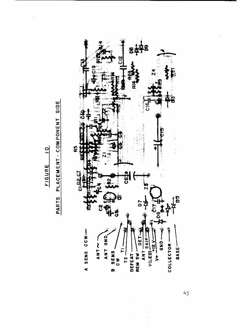
a m 0 W W O K 0
c
45

FIGURE I I
PARTS PLACEMENT- F O I L S I D E
'-IP 23 tR2 C 1 4 ~ R22
'4 RIG- RIS- CI 2 ------1t
I
w -- I Y l
/ B
L T I ____I__
SENS c w T 2
' * I S L J E - -b . - -DEFEAT
l R E M - DET SW
J( R'2 - - R23
07 25 + -"(LED) KIP ANT
-+ I2 v 0 L C 1 ' D 6 , # T 04 - G N D V+
T O8 * R14 +
09
la- +A&
R 9
+ --bc - COLLECTOR D 3 - -BASE D 5

FIGURE 12
ANTENNA CONSTRUCTION
NOT TO SCALE

FIGURE 13
ASSEMBLY DRAW1 NG

49

4PPENDIX B
PARTS L I S T AND SOURCES O F SUPPLY
Parts L i s t and Recommended Spare Par ts
Sources of Supply
PAGE
s1
56

PARTS L I S T
PART DESIGNhTION DESCRIPTION, MANUFACTURER, PART NO.
R1929 5,16 RESISTOR, 10K OHM, CARBON COMPOSITION OR CARBON F ILM, 1/4 WATT, 10% TOLERANCE OR BETTER, MFR. STCICKPOLEB PfiNCISONIC, OTHERS
R 3 RESISTOR, 220 OHM, AS ABOVE R 4 RESISTOR, 180 OHM, AS ABOVE R 6 RESISTOR, 68K OHM, CIS ABOVE R 7 , 10, 15,22 RESISTOR, l 00K OHM, AS M O V E R 8 RESISTOR, 4.7K OHM, CIS ABOVE R9,14, 20,219 23 RESISTOR, 1K OHM, AS ABOVE R11,24(NOTE 1) RESISTOR, 1M O H M , AS ABOVE R 1 2 RESISTOR, 220K OHM, AS ABOVE 1
R 1 3 POTENTIOMETER, l 00K OHM, LOCKING SHAFT CLARO 53C2-100K SUB OHMITE CLU-1041
CLARO 53C3-250K SUB CLARO S3C1-250K AND CUT SHAFT TO 1/2"
CLARO J3C2-1M SUB OHMITE CLU-1052
R 1 7 POTENTIOMETER, 250K OHM, P L A I N SHAFT
R 18,19 POTENTIOMETER, 1M OHM, LOCKING SHAFT
f f NOTE: 1K=1,000 lfl=l, OOO,000 ** $$ NOTE: SUB=SUBSTITUTE PERMITTED t f
C1,7,10,14,16 CAPACITOR, D I S C CERAMIC, 0.01 MICROFARfiD, SO VOLT CRL UKSO-103 SUE CRL CK-103
0.0047 MICROFARAD, 10% TOLERANCE, SO VOLT CRL CW 1 SC472K SUB CRL CW15A472K
10X TOLERANCE, 1000 VOLT CRL DD-500 SUB CRL DD-510
C2,3 CAPACITOR, MONOLITHIC, TEMPERATURE STABLE,
C4,11 CWACITORB DISC CERAMIC, 50 PICOFARADS
cs CAPACITOR# MONOLITHIC, TEMPERATURE STABLE, 100 PICOFARAD, 10X TOLERANCE, SO VOLT CRL C N l S A l O l K SUB MAL CK05BX101K
SPRAGUE TVA-1160.6 SUB SPRAWE TVA-1207.7
C 6 (NOTE 2) CAPACITOR# ELECTROLYTIC, 200 MICROFARAD, 16 VOLT

C 8
C 9 (NOTE 3)
C12,13
C 1 5 (NOTE 4)
C17,19
C 1 8 (NOTE 5 )
CAPACITOR, MONOLITHIC, TEMPERATURE STABLE, 0. 01 MICROFARAD, 10% TOLERANCE, 50 VOLT CRL CW15C103K SUB HAL CKOSBX103K
0.018 MICROFARAD, 10% TOLERANCE, 50 VOLT HAL CKOSBX183K SUB CRL CW20Cl83K CAPACITOR, METAL FILM,
CDE WMFOSP47-10 SUB CDE WMFOSPS-10 SUE CDE WMFlP47-10 SUB CDE WMFlPSO-10
SPRAQUE TVA-1160 SUB SPRAGUE TVA-1207 CAPACITOR, DIPPED TANTALUM, 1 MICROFARAD, 35 VOLT SPRAGUE 196D105X9035HAl SUB SPRAGUE 196D105X9050HAl SUE PANASONIC ECS-F35E1
0.001 MICROFARAD, 10% TOLERANCE, 1000 VOLT CRL DD-102 SUE SPRAGUE 5GA-Dl0
CAPACITOR, MONOLITHIC, TEMPERATURE STFIELE,
0.47 TO 0.5 MICROFARAD, 10% TOLERANCE, 50 VOLT
CAPACITOR, ELECTROLYTIC, 100 MICROFARAD, 16 VOLT
CAPACITOR, D I S C CERAMIC,
C20,21(NOTE 6) CAPACITOR, D I S C CERAMIC, 0.1 MICROFARAD, 50 VOLT CRL UK50-104 SUB CRL CK-104
CRL CK-203 SUB CRL UKJO-223
C 2 2 (NOTE 6) CAPACITOR, D I S C CERAMIC, 0.02 MICROFfiRAD, 50 VOLT
L1 ANTENNA C O I L - SPECIAL CONSTRUCTION (SEE TEXT) L2 (NOTE 7) HfSSH CHOKE, 500 MICROHENRIES, 0.26 OHM
MILLER 5256 SUB ANY SPWLL E-CORE CHOKE, APPROX. 1 TO 4
MILLIHENRIES, 1 AMPERE, TAB MOUNT
D1,2,8,? RECTIF IER DIODE, 1N914 (OE, FA11 D3,7 ZENER DIODE, 6.8 VOLT, 1 WATT, 1N4736A (MOT, TEL) D 4 RECTIF IER DIODE, 1N4007 (MOT) DS, 6 ZENER DIODE, 16 VOLT, 1 WATT, 1N4745CI (MOT, TEL)
Ql 612
z 1
TRANS I STOR, 'PNP , 2NS355 ( C3E, MOT 1 TRANSISTOR, PNP POWER DARLINGTON, TIP-126 (MOT, T I )
INTEGRATED CIRCUIT, PHASE LOCK LOOP RCA CD4046EE SUB MOT MC14046BCP

22
23
24
Z!3
s1
P1 J l P2 (NOTE 8) J2 (NOTE 8 )
53
P4eJ4
M1,2,3 M4,S M 6 M 7
MB M 9
MlOa, b,c
M 1 1 M 1 2 M 1 3 M 1 4 M1S
M1&-19
M 2 0 M 2 1
INTEGRATED CIRCUIT, OPERATIONAL AMPLIFIER RCA CA3130AE SUE RCA CA3130AS SUB RCA CA3130E, -S, -BE, -BS INTEGRATED CIRCUIT, DUAL TIMER RCA CD4538BE SUE MOT MCl4538ECP INTEGRATED CIRCUIT, HEX INVERTING BUFFER RCA CD4049BE OR -UBE SUB MOT MC14049BCP INTEORATED CIRCUIT, VOLTAGE REOULATOR, 8 VOLT MOT MC78LOBCG SUB MOT MC78L08ACG SUB W T MC78L08CPs -ACP (DIFFERENT LEAD PATTERN)
SWITCH, MINIATURE TOGGLE, SEALED HANDLE, DPDT ALCO MTE-206N
JACK, "RCA PHONO", SWC 3501F PLUG, OCTAL, AMPHENOL 86-CP8 JACK ASSEMBLY, OCTAL, WITH FLANGE AND RETAINER AMPHENOL 78RS8 JACK, MINIATURE 1/8 INCH, ENCLOSED, SWC 1426 SUE SWC 41 TWO CONDUCTOR POLARIZED CONNECTOR SET COLE-HERSEE 11172 (AUTOMOTIVE PARTS STORES)
PLUG, "RCA PHONO", SWC 3502
L I G H T E M I T T I N G DIODE, GENERAL INSTRUMENTS CMD-5022 FUSE HOLDER, BUSS HKP ENCLOSURE, BUD SC-3032 SOLDER, E R S I N "MULTICORE" OR OTHER H I G H QUALITY '* RAD 10" SOLDER TERMINAL STRIP, TRW J 6 A SOCKET, 8-PIN DUAL INLINE AUGAT 208AG29D SUB HAL DILB8f11 SOCKET, 16-PIN DUAL INLINE A W T 216AG29D SUB MCIL D I L B 1 6 P l 1 FUSE, BUSS A6C 1/2 FUSE, BUSS AGC 5
KNaE, KURZ-KASCH S-292-1L SCREW, NYLON, #&-32 X S/8", ROUND HEAD SMITH 2524 SUB CONCORD 701-6626
#4-32, 5/8" LONG, Si l ITH 8424 SUE CONCORD 6356-7610-19 c.csP FOR 52, AHPHENOL 86-3-24 TERMINAL STRIP, MINIATURE, SMITH 1075 SUB CONCORD 707-5129
HOOKUP WIRE, 22 AWG STRANDED, BELDEN 8524
STANDOFF, ALUMINUM, 1/4" HEX, INTERNAL THREAD
53

M 2 2 M23
M24
M 2 5
M26
M27 M28 M29 M30a, b, c
M 3 1
M 3 2 M33 M 3 4
a
M3S
M 3 6
M37
M38 M39
M40
M 4 1
" S P A W E T T I " WIRE INSULATION, 1/16" I.D. FASTENERS, STEEL, PLATED
a.SCREW, PAN HEAD, #6-32 X 1/4" 14 REQ. b.LOCKWASHER, INTERNAL TOOTH, 86 11 REQ. c.NUT, HEX, #6-32 6 REP. d.SCREW, ROUND HEAD, #2-56 X 1/4" 2 REQ. e . LOCKWASHER, INTERNAL TOOTH , #2 3 REQ. f .NUT, HEX, #2-56 2 REQ. g.FLAT WCISHER, 3/8" 1.D. X 11/16" OmDm 4 REQ.
MOUNTIN(3 HCSRDWRE FOR Q2 (MICA INSULATOR, STEP
WIRE, MAGNET, FOR L2, BELDEN 8073 (1 LB. ROLL MAKES THREE ANTENNAS) PAINT, FOR ENCLOSURE TOP, ANY SPRAY ENAMEL SUCH AS RUST OLEUM 7745 SUNSET YELLOW PRINTED CIRCUIT BOARD (SPECIAL-SEE FIGURE 14)
SPRAY FINISH FOR M28, DATAK 04177 MOUNTING HARDWARE FOR M1,2,3 GENERAL INSTRUMENTS CMP-22
BELDEN 8760 (ABOUT 17' PER ANTENNA) SHRINK TUBE, 1 / 2 " X 1 7/16" LONG, ALPHA F I T 221-1/2" SHRINK TUBE, 1/8", ALPHA F I T 221-1/813
CLEAR, STRAIGHT, 17" LONG POTTING MATERIAL FOR L1 ANTENNA, USE ANY R I G I D - SETTING EPOXY SUCH AS THAT USED TO INSTCILL SRPMs
(J2 REQUIRES 19") WIRE, BLACK, AUTOMOTIVE PRIMARY, 16 AWG (J2 REQUIRES 19") HEAT S INK COMPOUND, GENERAL CEMENT DC-Z(7 AUXILLIARY A I R VALVE, 12 VOLTS DC, NORMALLY-OPEN, THREE-WAY, FLANGE MOUNT, 1 /4" ORIFICE, HUMPHREY 250E1-3-11-21-35-61 (12VDC) MUFFLER FOR PROTECTION OF M39 EXHAUST PORT FROM D I R T ENTRY, SINTERED BRONZE, HUMPHREY EM2
CIND FASTENERS FOR INSTALLATION OF M39
WASHER, SPACER), RCA KC318
TRANSFER LETTERS, DATAK 9601
WIRE, 2 CONDUCTOR SHIELDED, FOR L l
WOOD FOR MAKING ANTENNA L1, STANDARD 2x6" PLANK,
WIRE, RED, AUTOMOTIVE PRIMARY, 16 AWG
1/4" I D HOSES, NIPPLES, CLAMPS AND OTHER F I T T I N G S

NOTES:
1. 2. 3.
4. 5.
6.
7.
8.
PRIOR TO SERIAL #107 R24 WAS l 0 0 K OHM PRIOR TO SERIAL # lo7 C 6 WAS 640 MICROFARAD PRIOR TO SERIAL #lo7 C 9 WAS 0.2 MICROFARAD D I S C CERAMIC. THE CHANGE WAS MADE NECESSARY BY PART MANUFACTURER’S
PRIOR TO SERIAL #107 C1S WAS 1000 MICROFARAD PRIOR TO SERIAL #lo7 C 1 8 W S 220 PICOFARAD. THE CHANGE WAS MADE TO SUPPRESS A SLIGHT BLOW I N LED M I UNDER NORMAL CONDITIONS FOR SOME UNITS. C20,21 CIND 22 WERE ADDED AFTER SERIAL # lo6 TO IMPROVE NOISE IMMUNITY. PRIOR TO SERIAL #107, L2 WAS A SMALL E-CORE UNIT AS DESCRIBED. CHANBE OF CHOKE L2 AND REVISED MOUNTING OF L2 WERE MADE NECESSARY BY PART MANUFACTURER’S DROPPING THE PART. P2 AND 52 ARE TO BE MODIFIED AS DESCRIBED I N THE TEXT.
CHANGE I N SPECIFICATION FOR THE PART.
R24, C& AND C l S NEED NOT BE CHANGED UNLESS A PROBLEM ARISES WITH UNDESIRED SKIPS AT TURN-ON. I N THAT CASE, UPGRADE A L L THREE PARTS.
L I S T OF RECOMMENDED SPARE PARTS
ONE EACH: P l ~ J 1 ~ Q l ~ Q 2 ~ Z 1 - Z 5 ~ D 6 ~ R l 3 ~ R l 7 ~ R l 8 / l 9 ~ L l ASSEMBLY, S1 ,M1 l r M 1 2

SOURCES OF SUPPLY
This l i s t w i l l i d e n t i f y the manufacturers given i n the p a r t s l i s t , some of which were given abbreviated names t o save space. Sourcex 1984185 ed i t ions of 501d Eook and EEM.
1 . ELECTRONIC DESION' S "OOLD BOOK" M Y D E N PUBLISHING COMPCINY 50 ESSEX STREET ROCHELLE PARK, NJ 07662 201-845-0550
2. EEM, ELECTRONIC ENGINEERS MCISTER HECSRST BUSINESS COMMUNICATIONSS INC./UTP D I V I S I O N 645 STEWART AVE. GARDEN CITY, NY 11530 516-222-2500
ALCO ELECTRONIC PRODUCTS, INC. 1551 OSGOOD ST. N. ANDOVER, HA 01845 617-685-4371
ALPHA WIRE CORP. 711 LIDGERWWD AVE. P.O.BOX 711 ELIZABETH, NJ 07207 201-925-8000
AMPHENOL, AN A L L I E D CO. 2122 YORK RD. OAK BROOK, I L 60521 312-986-1200
CWGCST, INC. 33 PEMY WE., BOX 779 ATTLEBORO, Mcs 02703 617-222-2202
BELDEN ELECTRONIC WIRE CIND CCIBLE P.O. B O X 1980 RICHMOND, IN 47575 317-983-5200
BUD RADIO
WILLOWHBY, OH 44094 216-946-3200 4605 E m 355th ST.
B U S S W DIV. (BUSS) P.O. 14460 ST. LOUIS, MO 63178 314-394-2877

CENTRALAB, INC. (CRL) 5855 NORTH GLEN PARK ROAD MILWAUKEE, W I 53209 414-228-7380
CLAROSTAT MFG. (CLARO) WFSSHINGTON ST. DOVER, NH 03820 603-742-1120
COLE-HERSEE COO (AVAILABLE I N AUTO PARTS STORES) 20 OLD COLONY AVE. BOSTON, flA 02127 617-268-2100
CONCORD ELECTRONICS 30 GREAT JONES ST. NEW YORK, NY 10012 212-777-6571
DATAK CORP. 65 71st ST. GUTTENBURG, NJ 07093 201-869-2200
F A I R C H I L D CAMERA AND INSTRUMENT CORP. (FA11
MOUNTAIN VIEW, CA 94042 413-962-5011 464 E L L I S ST., MS15-1035
GENERAL CEMENT 400 SOUTH WYMAN ST. ROCKFORD, I L 61101 815-968-9661
GENERAL ELECTRIC (GE) W. GENESSEE ST. AUBURN, NY 13021 315-253-7321
GENERAL INSTRUMENTS 600 W. JOHN ST. HICKSVILLE, NY 11802 516-733-3107
HUMPHREY PRODUCTS KILGORE AT SPRINKLE P.O. BOX 2008 KALAHAZOO, H I 49003 616-381-5500
KURZ-KASCH 711 HUNTER DR. WILMINGTMU, OH 45177 513-382-0966
MALLORY C A P W I T O R CO. (HAL) 3029 E. WASHINGTON ST. INDIFSNAPOLIS, I N 46201 317-636-3353
J . W . H I L L E R DIV., BELL INDUSTRIES 19070 REYES CIVE. P.O. BOX 5825 RANCHO DOMINGUEZ, CA 90224 213-!537-S200

MOTOROLA SEMICONDUCTOR PRODUCTS (MOT) BOX 20412 PHOENIX, A2 85036 602-244-6900
OHMITE MFG. CO. 3601 HOWARD ST. SKOKIE, IL 60076 312-675-2600
PANASONIC IND'L. ELECTRONIC COMPONENTS BOX 1503 SECAUCUS, NJ 07094 201-348-7000
RCA SOLID STATE DIV. ROUTE 202 SOMERVILLE, NJ 08876 201-685-6000
Ha H m SMITH (KULKfi-SMITHS INCm 1 (SMITH) 1913 ATLANTIC AVE. MANhSQUAN, NJ 08736 201-223-9400
SPRAGUE ELECTRIC CO.
NO.ADAMS, MCS 01247 413-664-4411 481 MARSHALL ST.
STACKPOLE CORP. STACKPOLE ST. ST. MARYS, PA 15857 014-781-1234
SWITCHCRAFT, INC. (SWC) 5555 N. ELSTON CHICAGO, I L 60630 312-792-2700
TELEDYNE SEMICONDUCTOR (TEL)
MOUNTAIN VIEW, CA 94040 415-968-9241 1300 TERRA BELLA AVE.
TEXAS INSTRUMENTS, INC. ( T I ) BOX 225012-MS-84 DCSLLAS, TX 75265 214-995-6611
TRW CONNECTOR DIV. 1301 MORSE WE. ELK GROVE VILLAGE, I L 60007 312-981-6000

CIPPENDIX C
WAVEFORM PICTORIALS
Waveform 1 Waveform 2 Waveform 3 Waveform 4 Waveform 5 Waveform 6 Waveform 7 Waveform 8 Wave+orm 9 Waveform 10
PAGE
60 60 61 61 62 62 63 63 64 64
THE FOLLOWING PHOTOGRAPHS WERE MADE OF ACTUAL OSCILLOSCOPE TRACES FROM A WORKING PAINT-SKIP. PROBE CONNECTIONS CIND OSCILLOSCOPE SETTINGS ARE L ISTED FOR EACH WAVEFORM. UNLESS OTHERWISE NOTEDp
1. CHANNEL B I S THE LOWER TRACE, AND I S USED FOR THE TRIG8ER SIGNALc + SLOPE.
2. WAVEFORMS ARE TAKEN WITH RESPECT TO CHASSIS GROUND, DC COUPLED VERTICAL AMPLIFIERS.
3. INPUT IMPEDCINCE I S 1 NEGOHW I N PARALLEL WITH 20 PICOFARADS.
4. PAINT-SKIP CONTROL SETTINGSr
SPEED COMP 5 0 X DELAY 0% S K I P 90%
39

WAVEFORM 1
HORIZONTALP 1 MICROSECOND/DIVISION CHANNEL A: 2 VOLTS/DIVISION AT Q1 (COLLECTOR)
WAVEFORM 2
HORIZONTCICx 1 MICROSECOND/DIVISION CHANNEL At 2 VOLTS/DIVISION AT Ql (BASE)

^ .
0
WAVEFORM 3
HORIZONTAL: 1 MICROSECOND/DIVISION CHANNEL A; 2 VOLTS/DIVISION AT Q1 (EMITTER)
:----I--
WAVEFORM 4
HORIZONTAL: 1 MICROSECOND/DIVISION CHANNEL f i r 2 VOLTWDIVISXON A T 21 (PIN 14)

WAVEFORM 5
HORIZONTAL: 1 MICROSECOND/DIVISION CHANNEL A: 2 V O L T S / D I V I S I O N CIT Z 1 (PIN 1)
WCIVEFORH 6
HORIZONTFSL; 1 MICROSECOND/DIVISION CHANNEL FI: 2 V O L T W D I V I S I O N AT Zl (PIN 6 OR 7 )
62

WAVEFORM 7
HORIZONTAL: 20 MILLISECONDS/DIVISION CHANNEL A: 1 VOLT/DIVISION AT Zl (PIN 10) CHANNEL B: S VOLTS/DIVISION AT Z2 (PIN 6 )
0
0
WVEFORM 8
HORIZONTALz 20 MILLISECONDS/DIVISION CHANNEL Ar 5 VOLTWDIVISION 6T 23 (PIN 6) CHANNEL B t 5 VOLTS/DIVISION AT 22 (PIN 6 )

0
0
WAVEFORM 9
....
HORIZONTAL8 50 MILLISECONDS/DIVISION CHANNEL A: 5 VOLTWDIVIS ION AT Z 3 ( P I N 10)
CHANNEL B I 5 VOLTS/DIVISION AT 2 3 ( P I N 6)
f I .... .... . . . . . . . . . . , . . . . . ... . . . . , . . .
0
I 1 I I I
WGVEFORM 10
HORIZONTALx 50 H I L L I S E C ~ N D S / D I V I S I O N CHANNEL A: 10 VOLTS/DIVISION AT 42 (COLLECTOR)
CHANNEL B: 5 VOLTWDIVIS ION AT Z 3 (PIN 9 ) TR113GER IS CHANNEL B, - SLOPE

APPENDIX D
SEMICONDUCTOR CATALOG PAGES
PAGE
Q2-Transistor, PNP Power Darlington 66 Zl-Integrated Circuit, Phase Lock Loop 71 22-Integrated Circuit, Operational Amplifier 76
Z4-Integrated Circuit, Hex Inverting Buffer 90 23-Integrated Circuit, Dual Timer 81
ZS-Integrated Circuit, Voltage Regulator 94

NPN PNP
Rating
Collecror-Emmer Voluga Coilecror-eau V o i r m Emittar-8au Vo(rwJ.
Collbcror Currmt - Contlnuour Peek
TIP120 TIP125
TIP120. TIP121, TIP122. TIP125 TIP126 TIP127 Unlr
Svmbol
VCEO 60 80 100 Vdc VCB 60 80 100 Vdc VEB -5.0- Vdc
.c---- 5.0 - Ic - 0.0 -
TIP121 TIP126
B a u Curronc
Total Power Oiutoatlon 6 TC - 25OC Oerate a t m u 25Oc
Dorare above 25OC
Load Enww I1 1
Total Power Oirt~oat~on 6 TA - Z°C
Unclemoed Induct~ve
TIP122 TIP127
~
Ig -120- mAdc
-a- Watts -0.52- WPC c-- 2 0 - Warts - 0.016 - WPC
E - M - m J
REPRODUCED COURTESY OF MOTOROLA, INC.
TJ. T,,, Ooeratinp and Storage hrnctlon.
Tsmwnrure Renp.
I PLASTIC MED I UM-POW ER 1 1
C- -65 to +150 - OC
COMPLEMENTARY SILICON TRANSISTORS . . . designed for general-purpose amplifier and low-speed switching applications.
High DC Current Gain - hFE * 2500 (Typ) @ IC 4.0 Adc
Chnener ln la Thermal Rearmnee, Juncrlon to Cam Thermal Roorarrce. Juncrlon to A m b m r
DARLINGTON
COMPLEMENTARY SILICON POWER TRANSISTORS
a AMPERE
Symbd Max Unrt
1.92 OCW JA 62.5 OCW
(1 ) I c - 1 A. L - 100mH. P.R.F. - 10 HI. V c c - 2 0 V . R g ~ - 100n.
TA 10
0
~ ~~
'C FIGURE 1 -POWER DERATING
0 19 40 60 80 'UO 110 X O I60
STYLE I PIN I . 3ASE
2. COLLECTOR 3. EUITTER 4. COLLECTOR
CASE ZZlAQL T O M A I

TlPl20, TIP121, TIP122, NPN, TIP125, TIP126, TiP127, PNP
Collector-Emitter Sustaining Vo1t.o. (1) ( Ic - 100 mAdc. Ig - 0 ) TIP120, TIP125
TIP121, TIP126 TIP122, TIP127
TIPl20, TIP125 TIP121.TIP126
Collator Cutoff Current ~ V C E - 30 Vdc. Ig - 01 (VCE - 40 Vdc, Ig - 01 (VCE 50 Vdc, Ig - 0 ) TlP122. TIP127
Collector Cutoff Current TIPlZO, TIP125 TIP121. TIP126
(Vcg -60Vdc. I € -01 (Vcg - 80 Vdc. IE = 01
I
Vdc - VCEO(rur)
60 80 - 100 -
ICE0 mAdc 0.5 0 5 0.5
'CEO mAdc - 0.2 - 02
- - -
(Vcg 100 Vdc. I E - 01 TlP122. TIP127 Emitter Cutoff Current
~ V R E - 5.0 Vdc. lr - 01 I 0.2 - mAdc - i 2.0
'EEO I -- 1 I 1 I I I
ON CHARACTERISTICS (1)
I DC Current Gain I h c c I I I - 1 (IC 0.5 Adc. VCE = 3.0 Vdc) llc 3.0 Adc. VCE - 3.0 Vdcl
tic 3.0 Adc. Ig - 12 mAdcl Collccror-Emitrer Saturation Voltage
l o o 0 - loo0 -
Vdc - I 2 0 VC E I ra t )
(1c - 5.0 Adc. Ig = 20 mAdct Baw.Emirtcr On v01Z.o.
(Ic 3.0 Adc, VCE * 3.0 Vdc)
FIGURE 2 - SWITCHING TIMES TEST CIRCUIT
4 .O - VBEionl VdC
- 2.5
*< : I . .
Smell-Signal Current Gain
Output Csoecitance (Ic - 3.0 Adc. VCE - 8.0 Vdc. f = 1 .O MHz)
(Vcg - 10 Vdc. I E - 0 . t - 0.1 MHz) TtP125. TlP126. TIP127 TIP12O. TIP121. TIP122
1 hfe - 8 .o - coo PF - 300 - I 2w

TIP120, TIP121, TIP122, NPN, TIPl25, TIP126, TIP127, PNP
FIGURE 4 - THERMAL RESPONSE
L J C I l l rl t l b J C 0 JC - 3 1250 C?n MIX
o cunvEs A m y F O R POWER PULSE TRAIN SHOWN REAO TIME AT t i
- . I a k l - TC a PIO~I GJCI~, O U T Y CYCLE 0 = 11 12
5w l o t 50 100 200 Y 0 ' 0 20 0 0 1 002 3 0 5 0 1 0 2 I 5 3 2 0 * i UE -5,
FIGURE 5 - ACTIVE-REGION SAFE OPERATING AREA
I . '302, , I ; ( I 0
s o
2 0
10
0 5
0 7 - - - o I-SECONO~REAKOOWNLIMITEO I I I I I I I I - " u 0.1 CURVES APPLY BELOW RATED VCEO
n n& I , TlP lZ l TIP126. : - ! I I ". 0021 1 : 1 I [ { I TIP122 TIP127 f ; :
I 0 1 0 3 0 5 0 7 0 1 0 20 30 5 0 7 0 1 0 0
VCE COLLECTOR EMITTER VOLTAGE (VOLTS1 .
FIGURE 6 - SMALLSlGNAL CURRENT G A I N
1 0 2 0 3 0 D 20 50 I00 200 500 Joo
' FREOUENCY I L t i i l
There are rwo limirarionr on the Dower handling aoilitv of a transistor average Iuiution temoerature and IQCOnd breakdown Safe oonatiog area C U N ~ moicate 1c - VCE Itmirr 01 the van. sistor fhar must beobserved tor reigacle werocion. I c.. rhe transistor must not be sublected to geater amoat ion tnan rnecurvcr indicate
The data of Figure 5 1s oasea on T J ( o t l - 150%. T c *svrriaOle deoending on conditions Sacono Ireahdown oulla l imtrs are valld
calculared from the dara on Flgure 4 A t ntgn case rem~erarurer. thermal timitations wtll reduca :nc Dower rnar can be handled to vaiues lass then the Iirnitarlonc ammwd by =and breakdown
for du ly CVCleS tO PfOvlatO T J ( ~ * ) < 15OOC T j (ok ) may be
FIGURE 7 -CAPACITANCE

TIP120, TIP121, TIP122, NPN, TlP125, TIP126, TlP127, PNP
NPN TIP120, TIP121, TIP122
FIGURE 8 -
0 1 0 2 0 1 0 5 0 7 1 0 2 0 3 0 5 0 7 0 10
It. COLLECTOR C U R R E N T (AMPI
FIGURE 9 - COLLEC
0 3 0.5 0 7 1 0 2.0 3.0 5.0 7.U 10 20 30
18. BASE C U R R E N T ImA)
PN P TIP125, TIP126, TIP127
EURRENT GAIN
lr COLLECTOR iJSRENTlAMPI
SATURATION REGION
In BASE C U R C E \ T lmAl
' VOLTAGES

NPN TIPlZO, TIPl21, TIP122
FIGURE 1 1 - TEMP
- so l 0 1 0 2 0 3 0 5 0 7 10 2 0 30 5 0 I0 10
Ic. COLLECTJR CURRENT 'AMPI
FIGURE 11 - COLLE
105 I
V ~ E . EASE EMITTER VOLTAGE IVOLTSJ
FIGURE 13 - OAR1
PNP TIP125, TIP126. TIP127
rURE COEFFICIENTS
I I ' , I ' 1 1 ; ' I -5 0 -
I
0 1 0 2 0 3 0 5 1 0 i J ; J $ 2 7 0 10
I t . COLLECTOR CURRENT (AMPI
- - 5 0
R CUTOFF REGION
105
104 t
V g c EASE EMITTER VOLTAGE [VOLTS)
TON SCH€MATlC
COLLECTOR PNP
TIP126 r------ TIP125
r TIP121 ;
6 EMITTER

REPRODUCED COURTE8Y OF MOTOROLA, INC.
@ MOTOROLA
PHASE-LOCKED LOOP
The MC14046B phase-locked loop contains two phase compara tors, a voltagecontrolled oscillator (VCO). source follower, and Zener diode. The comprrators haw two common signal inputs. PCAin and PCBin. Input PCAin o n be used d i m l y coupled to large voltage signals, or indirectly coupled (with a series capacitor) to small voltage signals. The self-bias circuit adjusts smal l voltage signals in the linear region of the amplifier. Phase comparator 1 (an exclu- sive OR gate) powides a digital error signal PClout, and maintains 900 phase shift at the center frequency between PCAin and PCBin signals (both a t 50% duty cycle). Phase comparator 1 (with larding edge sensing logic) provides digital error signals PChut and PCPout, and maintains a phase shift between PCAin and PCBin signals (duty cycle i s immaterial). The linear VCO produces an output signal vcoou t whose frcquency is determined the volt- of input VCOin and the capacitor and resistors connrcted tO pior CIA, ClB. R 1 . and RZ. The lourcc-follower output SF,t with an external re- sistor i s used where the VCOin signal is needed but no lording u n be tolerated. The inhibit input Inh. when high. disables the VCO and source follower to minimize standby power consumption. The Zener diode can be used to assist in power supply regulation.
Appliutions include FM and FSK modulation and dmodulation, frequency synthesis and multiplication. frequency discrimination. tone decoding, data synchronization and conditioning, voltage-to- freguency conversion and motor speed control.
VCO Frequency - 1.4 MHr Typical @ VDD
0 VCO Frwuency Drift with Temperature = 0.049CPC T y p d @ VDD = 10 Vdc VCO Linearity = 1% Typical Quiescent Current = 5.0 nA/package typical @ 5 Vdc Low Dynamic Power Dissipation - 70 pW Typical 8 fo - 10 kHr. V ~ ~ = 5 . 0 V d c . R 1 = 1.0Mn. R Z = m , R ~ ~ w O D Buffered Outputs Compatible with MHTL and Low-Power TTL Diode Protection on All Inputs Supply Voltage Range = 3.0 to 18 Vdc Pin-forPin Replacement for C040468
10 Vdc
BLOCK DIAGRAM ----------------- 2 ?Clout *h.r
Crcvir como.r.tor 1
MC14046B 1
CMOS MSI ILOWPOWER COMPLEMENTARY MOS)
PHASE- LOCK ED LOOP
L SUFFIX P SUFFIX CERAMIC PACKAGE PLASTIC PACKAGE
CASE 620 CASE 648
ORDERING INFORMATION
MCl4xxx8 Suttt i Oonotai
L Cmrmnic Pack.- P *imt*c P.c*.o. A E a n r n n d Ooeroting
TompraNra Ronga C Limitod Owrat ing f T m w o t u r a Ran-
71

MC14046B
DC Suoolv Volriqc
lnout Volta-. All Inputs
QC Currtnr Drain Dcr Pm Omrating Tempraturc Ranp. - A L Device
Storage Temwrature Ranw
CLICP Deve.
MAXIMUM RATINGS (Voltages referenced ro V s s l
r Rattno 1 Svmbol I Value I Unit 1 VDO 1 -05ro -18 I Vdc
V,, I - 0 5 t o V ~ o + 0 5 Vdc I 10 m Aac
T A -55 10 + I 25 OC
T,,, -65 to -150 OC -40 ro -85
TIOW. 25% voo ChU-K Svmbol Vdc Min . Mar Min Typ Mar
Ourour V o I r w "O"LIWI VOL 5.0 - 0.05 - 0 0.05 Vin = VDO or 0 .. 10 - . 0.05 - 0 0.05
"1" L m d V a n 5.0 4.95 - 4.95 5.0 - v,n ' 0 Or VDO 10 9.95 - 9.95 10 -
15 14.95 - 14.95 15 - I V o - 4.5 or 0.5 Vdcl 5.0 1.5 2.25 1.5
10 - . 3.0 - 4.50 3.0
15 - 0.05 - 0 0.05
Inout Voft-. "0" Lave1 VI L - -
Th*. Min Mar
- 0.05 - 0.05 - 0.05 4.95 - 9.95 - I495 - - I .5 - 3.0
( V o =0.5 w4.5 Vdcl
(vo - 1 5or 13.5 Vdcl ( V O = 1 .o or 9.0 Vdcl
- Outour Drw8 Current I A L Davser IDH
5.0 ' (VOH - 2.5 vdc l SOUrCe (VOH * 4.6 Vdcl 5.0 I V o n - 9.5 Vdcl 10
(VOL - 0.4 Vdcl Sink IOL 5.0 (VOL - 0.5 Vdcl 10
W o n 13.5 Vdcl 15
( V O L - I 5 Vdcl
(VOH 2.5 vdc) Source 5.0 (VOH 4.6 Vdcl 5.0 ( V n u - 9.5 Vdcl 10
15 Output Drtw Cwrent (CLICP & w e 1 IOH
3.5 - * 3.5 2.75 - 3.5 - 7.0 5.50 - 7.0 - 7.0 - - 11.0 8.25 - 11.0 - 1 1 .o
-1.2 - -1.0 -1.7 - -0.7 - 4.25 - -0.2 -0.36 - -0.14 .( - 4.62 - -0.5 -0.9 - -0.35 - -1.8 - -1.5 -3.5 - -1.1 - 0.64 - 0.51 0.88 - 0.36 - - 0.9 1.6 1.3 2.25 - 4.2 - . 3.4 8.8 - 2.4 -
-1.0 -0.6 - -0.2 - -0.16 -0.36 - -0.12 - -0.5 - -0.4 -0.9 - -0.3 -
-
- -0.8 -1.7 -
- Unit
Vdc
- Vdc
- Vdc
Vdc
- m A a c
7
mAdc
7 2

MC140468
Minimum Marmum V o o AL CLICP T v ~ l u l AL CLICP
Ch..ccWUllC Symbol Vdc W Owur AII1yp.r Ow- Owlcr Unns
Output Rise T i m tTLH nr - - 180 350 400 l TLH - (3 0 nrloFF) CL + 30 m tTLH - I1 5 m l d l CL + 15 m 'TLH - (1 1 nsloFI CL + 10 nr 15 - - 65 110 160
~ T H L - 10 75 nrloF1 CL + 12 5 m 10 - - 50 75 100 tTHL - (0 55 ns/oFl CL + 9 5 nr 15 - - 37 55 80
5.0 10 - - 90 150 Mo
Output Fall T i m ~ T H L nr - ~ T H L (1.5 nr/pFl CL + 25 nr 5.0 - 100 175 200
i
- PCB., I - Minimum lnout SenrittvitV Van 5 0
15 - AC Cou@sd - PCA,, 10 - C serm - 1OOOoF. t - 50 k H z
I - 200 300 400 m v p p 400 600 800 700 1050 1400
- -
7 3
DC COUDled - PCA,,. PCB,, - St0 15 See Noise lmmunitv
Maximum Freauency fmax (VCO,, VDD C1 - 50 OF R 1 - 5 k R a n d R 2 = - l
(RZ - -I - Temperature - Frequency Stability
- Linur t tv (R2 - -1 (VCO,,- 2 5 O V : 030 V, R l > 1Okf:l lVCOtn 5 00 V t 2 50 V. R 1 > 400 kRJ IVCOln - 7 50 v t 5 00 V. R1 > loo0 kRI
Output Dutv Cvclc -
5 0 050 035 0 7 0 - - M W z 10 10 0 7 14 - - 15 14 1 0 1 9 - - 5 0 0 1 2 - - X P C
0 0 4 - - 0015 - 10 15
5 0 - 10 1 - 15 1 - -
- - - - -
% - - - : I
1 - - - - -
- - 5 to15 - 50 - %
lnout Rmistantx - VCOIn I Rtn I 16 150 16 I 1500 I - I - I MR
Offset Voltage IVCO,, minus SFoul. RSF > 50 kRl
lVCOIn - 2 50 V : 0 30 V. RSF r' 50 kR1
fVCOIn - 7 50 V : 5 00 V, R S F > 50 kR)
L i near+ t y
( v c o i n - 5 w V: 2 5 0 v, RsF > 5 0 k R I
- - 5 0 - 165 2 2 2 5 vac 10 - 15
5 0 0 1 - - 10 0 6 - - 15 - 0 8 - -
- 165 2 2 2.5 165 2 2 2 5 - -
- 'c - - - - -

MC140468
FIGURE 1 - PHASE COMPARATORS STATE DIAGRAMS
PHASE COMPARATOR 1
PHASE COMPARATOR 2
I I
Refer to Wweforms in Figure 3.
FIGURE 2 - DESIGN INFORMATION
Locks on harmonica of emtor frwwnc
Wm: 1OK<R1 C 1M 10K < R 2 < 1M loo06 < c 1 < .01 rrF
I

MC140468
FIGURE 3 - GENERAL PHASE-LOCKED LOOP CONNECTIONS A N 0 WAVEFORMS
Typiul Low-Pass Filtrs
Tyolcally :
Note: for further information. see: Ill F. Gardmr. "Phw-Lock Tuhnauer", John WiIev md Son. New York. 1966. (21 G. S. Mouhytz, 'Minuture RC Filten Using Phase-Locked LOOP". ESTJ, May, 1965.
(3) Ganh Nnk. *'PhN-LOfk L m M i g n Fundunentalr". AN-535. Motorola Inc.
Waveforms Phew COmMretOr I
PCIWI _ n _ n _ n _ n _ ' O " vo L
nUw Commarator 2
- VOH
- VOL
VCOin ,
75

REPRODUCED COURTESY O F RCA CORPORATION
CA3130, CA3130A, CA3130B Types
BiMOS Operational Amplifiers
Features: MOSIFET input r u g . provides:
wry hi* 21 - 1.5 T n (1.5 x lo1* WP. very low I1 - 6 PA typ. a t 16-V operation With MOS/FET Input, COS/MOS Output
RCACA313OT. CA313OE. CA3130S. CA- 31 30AT.CA3130AS.CA3130AE.CA31~8T. and CA3130BS are integratedcircuit oper- ational amplifiers that combine the rdvan- cages of both COSlMOS and bipolar t r m . istors on a monolithic chip.
Cuto-protected p m n n e l MOSlFET (PMOS1 transistors are used in the input circuit to provide wry-high-input impedance. wrylow- input current. and exclotional spced per- fornuno?. The use of PMOS ficldiffect transistors in the input stage results in common-mode input.volt.ge capability down to 0.5 volt below the ncgltivewpply ter- minal, an important attribiite in single.supply applications.
A ~mplementarv.symrnerry MOS lC0Sl MOS] transistor-pair. capable of swinging the output voltage to within 10 millivolts of either supply.voltage terminal (at very hlgh values of load impedanal. is employed as the output circuit.
The CA3130 Scries circuits operate n suppiy voltages ranging from 5 to 16 volts. or $2.5 to t 8 volts when using split supplies. Thev can be phase comwnsated with a single ex- ternal capacitor. and have terminals for adjustment of offset volt- for applications
requiring offrt.nulI capability. Terminal pro- visions are also made to permit strobing of the output st-.
The CA3130 Series is supolied in standard &lead TO.5 style packages (T suffix). &lead dual-in4ine formed lead TO-5 style ''OIL- CAN" &ages (S ruffixl. The CA3130 i s available in chi0 form IH suffix). The CA3130 and CA3130A are also available in the Mini-DIP & l e d aual-in-line plastic package (E suffixl. All types operate o w the full military-temperature range of -55OC to +125%. The CA31308 is intended for applications requiring premiumgrade specifications and with limits ntablished for: input current, temperature coefficient of inout-offrct voltage, and gain over the range of -55OC to +125OC. The CA3130A offers superior input cnaracteristics over those of the CA 3 130.
I t . I
I ' I
I I i 1 I
1 I 1 I
ZWT I
I I I I I I
m LOW vIo: 2 mv MX. (CA313OB) W i b BW: 16 MHr ryp. (uniWg.in crorwrwrl High SR: 10 V/* typ. hitywin tollowwl High output cumnt (10): 20 mA tvp. High AOL: 320,000 010 dBJ typ.
m Compnution with tingle oxtomal capacitor
Applications: Ground-ratwenad unglcupply amplifiers Faat umpk-hdd a m ~ i f u r r Longduration timur/monort.blor High4nputimpedMa ~ m p m t 0 r S
High.inputimpdma widob~nd amplifier$
Ie.9.. toll- tor dnglcupply OIA converter1
(permits contml of output voltage down to MW dul
(ideal intorha with digital COSMOS1
Voltage follawr
Volup.rrgul.pon
Peak deraton m Single-wppk MI-wave prociaion rectifiers
Photo-diode m w r amptitiers

CA3130, C ,3130A, CA31308 Typer MAXIMUM RATINGS. Ibsoarur#-M~rrrmum
2C SUPPLY VOLTAGE 18.nw.n V' and V- T.rmm.kb . . . . . . 16 V
0IFFERENTIAL.MCIllF - - - - - - - INPUT VOLTAGE .................. t9 V
INPUTVOLTAGE.. . N + d V l m IV'4.5 V l COMMON-MOO€ M:
INPUT-TERMINAL CURRENT ......... 1 mA DEVICE DISSIPATION: WITWOUTHEATSINK -
UP TO 5 5 0 ~ ................... A8OVE 55OC .... ORW t i m w 6.67 mwPC
A T 125OC ..................... 418 mW BELOW 125OC ... Oarice l inrrly 16.7 mWPC
630 mW
W I T H HEAT SINK -
TEMPERATURE RANGE: OPERATING IalI NP.I ..... -66 m + 1 Z o C STORAGE I . 0 w m l - ...... -45 m + 150°C
OUTPUT s n o R i k i r i c u i i DURATION ? ............ INOEFINITE
LEA0 TEMPERATURE IOURING SOLDERINGI: AT OISANCE l I 1 6 f l l f l INCH I1.Y) 2 0.79 mml FROM WE FOR 10 SECONDS MAX. .... .ZOS*C
1 Maximum Output I 1 I I I l l I 1 I VoI1.KIe: 1 1 1 1 1 1 " . .....I I 1.) I , * ? I
,2 1
vow- - 0 10.01 - 0 0.01 - 0 0
v z - - 0 At R L = ~ kR
VOM* 14.99 15 I - 14.99 15 - 14.99 1s - .01 At RL" -
Maximum Output I
V
- Current:
IOM+ (Source) O 12 22 45 12 22 45 12 22 45 v o - o v mA
[OM- (Sink) 8 I V n = 1 5 V I 12 I 20 I 45 I 12 I 20 1 4 5 1 1 2 I 20 I 4 5 I I
I
1
-...., -..., .... . * I ..... I ...... ......... ~- . . . . . . ...-. ... ,

CA3130, CA3130A, CA3130B Types . TYPICAL VALUES INTENDED ONLY FOR DESIGN GUIDANCE
I TEST
CONDITIONS
v + - + 7 s v
CA31308 CA3130A CA3130 UNITS v- - -7.5 v
IUnlrss Other-
CHARACTERISTIC 1 TA -250c I 1T.S) 1 1T.S.E) 1 1T.S.E) 1 Input Offset Voltage Adjustment Range
IVoltagc
Follower I 1.2 1.2 1.2 US Settling Time (4 Vp.p
Input to <O.l%)
' Althoupn a 1 . ~ ~ 2 I O U ~ C ~ t i uud for Ihti ten. the eowvuew inwt not= remains constant for values of RS UD to 10 Mn
CONDITIONS ~
v * = s v j v - - 0 v '
CHARACTERISTIC T A m 2 5 0 C CA31308 CA313OA I ITS1 1T.S.EI (UnknOthcr. :
I wise Sp.cified1
Inour Onvr Voirage VIQ ! l 2 Inout Offset Currcn:. IIC 1 I 0.1 j 0.1 Inour Current. 1 1 I 1 2 I 2
CA3130 1T.S.E)
8 0.1 2
80 100 k
100
0 10 2.8
300
MI.. . . . . . . . . . . . . . . . . - .+. C.. ,.., . . 04 W l W I . O c I Y C I.*,.Vl . & _ . . '
- I V . 0
. . . . . . . . . . . . IC Ioc om. 00' c

CA3130, CA3130A, CA3130B Types CI RC'JIT OESCRIPTIOR
Fig. 3 s 3 5oct oiaqram of the CA3130 Ser:es CCSIMCS Ooerationai Amoiifiers. The inout :erminals may be ooerated down to 0.5 V below the negative suoolv rail. and the output can be swung very close to either supply rail in many applications. Consc- quently, the CA3130 Series circuits are ideal for singla-suooly owat ion. Thrsc C l a n A amplifier stages. having the individual win capability and current consumption shown in Fig. 3. provide the total gain of the CA3130. A biasing circuit provides two potent ia ls for common use in the first and second stages-Term. 8 can be used bofh for phase cornwnsation and to strobe the output stage into auiescena. When Term. 8 i s tied to the negative supply raii (Term. 4 ) by mechanical or s lmriul means, the output potential a t Term. 6 essentially rises to the positive supply-rail potential a t Term. 7. This condition of essentially zero current drain in the output nage under the rtrobed "OFF" condition can only be achieved when the ohmic load resistance presented to the amplifier isvery high k g . , when the amplifier outout i s used to drive COS/MOS digital circuits in cornoarator apdications).
lnpur Stages-The circuit of the CA3130 is shown in Fig. 1. It consins of a differential- input nag^ using PMOS field-effecl tran- sistors fQ6. 07) working into a mirror.pair of biwlar transistors 109. QlO) functioning as load resistors together with resistors R3 through R6. The mirror-pair transistors a h funnion as a differential-to-sin01e~nded con- vener to provide base drive to the second- stage biwlar transistor (01 1 ). Offset nulling. when desired, can be effected by connecting a 100,000-ohm wtentiometer across Terms. t and 5 and the potentiometer slider arm to Term. 4. Carcodeconnected PMOS transistors Qz. 0 4 are the constantcurrent source for the input stage. The biasing circuit for the constant~urrent source is rubrequentlv de- scribed. The small diodes 05 through 08 provide gate-oxide protecfion against high- voltage transients. e.g.. including static elec- tricity during handling for Q6 and 07.
second-Stage-most of the vol taq gain in the CA3130 is provided by the second amplifier stage. consisting of bipolar transistor Q1 1 and i t s carcodesonnested load resistance Provided by PMOS transistors 03 and a. The source of bias potentials for c h a r PMOS transistors is subsequently described. Miller- Effen cornomsation (roll-off) i s accom- Plished by simply connecting a Small c a M titor between Terms. 1 and 8. A 47.picofarad CIoacitor provider sufficient compensation for stable unityqain operation in m o s t aoplicationr.
Bias-Source Circuit-At total SUP@V voltages. Iornewhrt above 8.3 volts. resistor A 2 and Zener diode 21 serve to establish a VOlt.gc of 8.3 volts across the serierconoected circuit. consisting of resistor R l . diodes 01 through Do, and PMOS transistor 01. A fa0 at the iunction of resistor R1 and diode w provides a gate.bias potential of about 4.5 volts for
PMOS transistors Qj an0 CS rvt*n *?soect !o Term. 7 . A mtenttai 0: doou: 1.2 roits . I dcveiooea across dioouonnectec lMOS tram sistor 01 with respect to Term. 10 orovide gate bias for PMOS transistors Qz an0 03. It should be noted rhat 01 i s "mirrorcon- n.cted"T to both Q2 and 03. Sna tran- sistors Q 1 , Q2. 03 are drrigntd to k iden. tical. the aowoximately 2OO-micmamwre current in Q1 establishes a similar current in Q2 and 03 JS constantcurrent wurm for both the first and second amplifier stages. resoectively.
At total supply voltages somewhat les~ than 8.3 volts. Zener diode 21 becomes non- amdunive and tha potential. developad across series-cannccred A t . 01-04. and 01. varies direc:iv with vninions in suUPp(V voltage. Consequentlv. the gate bias for 04. 05 and 02. 03 varies in aceordance with wpp(y.voitage variations. T h i s variation re- sults in deterioration of the power-ruooly- rejection ratio (PSRR) a t total ruodv volt- ages below 8.3 volts. Operation a t total SUP-
ply voltages below awut 4.5 volts results in seriously degraded performance.
Output Stage-The outout stage consists of a drain-loaded invening arnaifier using COS/ MOS transistors ooerating in the Class A mode. When Operating into very hiqh resist. ance lords. the output can be swung within millivolts of either suooly rail. B a u s e the output stage is a drain4oaded amolifier, i t s gain i s dependent upon the load im-na. The transfer characteristics of me output stage for a load returned ro :he negative suppty rail are shown in Fig. 6. Typical OP- am0 loads are readilv drinn by the outout nage. Because Iarge-signal cxcursiom are nono linear, requiring feedback for good waveform reproduction. Rmsient delavs may be en- countered. As a voltage follower, the amdi- fiercan achieve 0.01 per cent accuracy levels. including the negative suoply rail.
Input Current Variation mth Common- M o 6 Input Volupr
As shown In the Table of Electrical Charac. teristiu. me input current foc the CA3130 Series OwAmos is tvpiolly 5 PA a t T~=25oC when terminals 2 and 3 are at a common- mode potential of +? 5 volts mth respect m negative SUOQIV Terminal 4. Fig 11 contains data showing the variation of inout current as a function of common-mode inout voltage at TA * 25OC. h e aata show m a t arcuit designers can advntageously exoloit these characteristiu to design arcuiu wnich tyw- cally require an inwt current of less than 1 pA. provided the common-mode input volt age does not exceed 2 volts. As Dreviwsly noted. the input current is essentially the result of the leakage current through the
gate-orotecrton diodes on :he mout circuit and. inereiore. a function ot tne aoplied
-I ~ " 1 I., I- #a . -.- Ftg. 11 - lnmr curmnr n. cammomnod# rQmfu.
voltaga. Although the finite resiswoc of the glass terminal-to-case insulator of the TO-5 package also contributes a n inuement of leakage current. there are useful comwnsa- ting fanors. Because rhe gate-motection net- work funnions as i f i t 6 connccfed to Terminal 4 potential. and the TO-5 case of the CA3130 is also mernally tied to Term- inal 4. input terminal 3 is essentially "guarded" from spurious leakaga currenrs. Offset Nulling Offset-voltage nullmg i s usually Kcomolished with a lW.000-ohm potentmmeter con- nected across Terms. I and 5 and with the potentiometer slider arm connecred to Term. 4 A fine offset-null adiurtment usuatlv can be effected with the dlder arm positioned in the mid-point of the wtentiomecer'r total
Input-Current Variation with Temperature The input current of the CA3130 series cir- c u m IS typicallv 5 pA a t 25OC. The mator portion ot this inout current is due to leakage current through the gate-orotectin diodes in the mput cmuit As with any sennconductor. junction oevice. including op am- with a lunction-FET mput stage. the leakage cur- rent aoproximately doubles for e n r v tO0c increase in temtxrature. Fig.12 povida data on the typlcal variation of inwt bras current as a funnion of temperature in the CA3130.
range
; ,t.A / 1 1
I - . ~ - w - - e a a m o w m m a 0 ~ -
U U e . 7 ? C M * . t ( C I I.,l-.c -... U.
Fq. I t - Inwr curnnr n mm4naw nnwuarur..
In apphcacions requiring the lowest practical Input current and incremental increase in
79

CA3130, CA3130A, CA3130B Types current because of "warm-up" effects. i t I S
suggested that an appropriate heat sink be used w i th me CA3130. In addition. when "sinking" or "sourcing" significant OutDut current the chip temperature increases, causing an increase in the input-wrrent. In such cases. heatlinking can also w r y mar- kedly reduce and stabilize input current variations.
Input-Offut-Vdtap (V~ot Variation wi th
It is well k n w that the churteristicr of a MOWFET device can change slightly when a dc wte-source bias potential is applied to the device for extended time periods. The mrgni. tude of the change is increased at high tem- peratures. Users of the ('33130 should be alert to the possible immcts of this effect i f the application of the dev ia involves ex- tended operation at high temPeratures wi th a signifion: differential dc bias voltsgc applied across Terms. 2 and 3. Fig.13 shows typical data pertinent to shifts in offset voltage encountered with CA3130 devices ( T O 4 package) during life testing. At lower tem- peratures (TO.5 and plasticl. for example at 85OC. this change in voltage is C o n - siderably less. In typical linear appliCa. tions where the differential voltage is Small and symmetrical. these incremental changes are of about the same magnitude as those encountered in an o w r a t i w l amplifier em- ploving a bipolar transistor input stage. The two-volt dc differential voltage example reo- resents conditions when the amplifier outnut stage is "toggled", e.g., as in comparator applications.
6i.S VS. k V * r w a t h q Life
Pomr-Supply Conaderations &cause the CA3130 is very useful in sinale rupply apolications. it i s pertinent to rcview some considerations rehting to power.ruodv amen( consumption under both siogle and dual-supply service. Figs. 14a and 14b show the CA3130 connected for both dud- and single-supply operation.
Dual-suoply ooeratim. whm the outoul roltage a t Term. 6 i s zerc-vdts. the currents supplied by the two power supples are w u a l When the gate terminals of 08 a n d 012 are driven increasingly wsitiyc mrh reswc :C pround. current f low through 012 ffron m e
negative supolv) 10 the load i s increased and current f low through 08 (from tne p o s i t i v e supply) decreases correswndinglv Wnen the gate terminals o f Q8 and 012 are driven in. creasingly negative w i th r e s m to ground. current f b w throuqh 08 i s increased and current f low through 012 is decreased accordingly. Single-supply operation: Initially. le t it be assumed that the value of R i s very high (or dirconnected). and that theinout-terminal bias merms. 2 and 3) i s such that the out- put terminal (No. 61 voltage i s a t V'2. i t . the voltagedrops across Q8 anc 0 1 2 are of equal magnitude. Fig. 7 shows tvpical guies. cent supplycurrent vs. supolv.voltagC for the CA3130 operated under there conditions. Since the output stage is ooerating as a Class A amplifier, the suppivsurrent will remain constant under dvnamic ooeraling conditions as long as the transistors are operated in the linear portion o! their voltage-transfer char r te r is t ia m e Fig. 6:. I f either 08 or 012 are w u n p out of the i r linear regions toward cut-off la nod inear regionl. there w i l l be a corresooncing r e duction in supplycurrent. Ir. the extreme case, e.g., w i th Term. 8 swuqg aown 13 ground potential (or tied to ground NhQS transistor 012 i s Comoletclv C U T of f and m e supplycurrent to series-connected lransislo'f 08. 012 goes essentially to zero. The two preceding stages in the CA3'30. howeve'. continue to draw modest supptv.curre?t 1%' the lower curve in Fig. 7 ) eve- tnough trw output stage i s strobed off. Ft;. 14a snows a dual-supply arrangement for IPC OU:XI stace that can also be strobed off, asr;min$ f i ~ ' ~ . by pulling the wten t ia l of Te*m. 8 c3wn I; that of Term. 4.
Let it now be assumed that a icad.res*stance of nominal value (e.g.. 2 kilc?ms: IS COP.
mcted between Term. 6 anc younc in :he circuit of Fig.14b. Let i t furrPt* be essumec again that the input-terminal D as (Te-mc. 2 and 31 is such that the OU~DU: :ermc-,ai l k . 6) vol~age is a V+/2. Since Ph'OS t:a?sis:o' 08 must now supply auiesce-t current :c both RL Md transistor 0 1 2 . i t should bc applrent that under these conditloqs tne IupOlycurrenr must increase as an inverw function of the R L magnitude. Fig. 9 shows the volttgc-drop across PMOS :ramistor 06 na func r iono f loadcurrent at Icveral SuPDIv. voltages. Fig. 6 shows the roi;rge.transfe- charrcteristin o f the output s:agc for Several values of )om resistance.
Wideband Not= From the standpoint of low.~otse Dcr fo r r ance considerations. the use o* me C.43133 1s mon advantageous in apo~cat ionr where in the source resistance of the mu ' signal 1s 10 the order of 1 m q o h m c' more In T ~ I S caw. the total input-referrec - w e voltaw IS r /pcZnv only 23 uV wher :*c teY circu : amolifwr of Fig. 15 1% ooe*a:ec a- a to:a' suodv rcftage o f 15 volts --s "a'ue ?' toial mput-referred noise re-; - I esse'ila \
constent. ever thougr :Pt . i - 5 c' s5-.::
resistance is raised by an order of magnitude T h i s characteristic is due to the fact that reactance of the inout capacitance becomes i significant factor in shunting the source resistance It should be noted. however. that for values of source resistance very much greater than 1 mqohm. the total noise voltage gemrated can be dominated bv the thermal noise contributions o f both the feedback and source resistors
80

i
REPRODUCED COURTESY OF MOTOROLA, INC.
inout Volmge. A l l Inputs
DC Current Drain per Pin
Gwrrting Tmoeraturc R a w - AL Device
@ MOTOROLA
Vtn 1 - 0 5 t o V ~ ~ + 0 . 5 Vdc
I 10 rnAac TA I -55 to -125 oc
DUAL PRECISION RETRIGGERABLE/RESETTABLE MONOSTABL E MU LTlV I BR AT0 R
- CLlCP Dcvlcc I
The MC145388 is a dual. retriggerable. resettable monostable multivibrator. It may be triggered from either edge of an input pulse, end wil l produce an accurate output pulse over a wide range of widths, the duration and accuracy of which are determined by the external timing components, C x and Rx. Linear CMOS techniques allow more precise control of output pulse width.
I
--40 to + i 5
21 0% Typical Pulsewidth Variation from Part to Part
20 5% Typical Pulsewidth Variation over Temperature Range
New Formula. T = R C (T in seconds. R in ohms, C in farads)
Pulse Width Range = 10 ps 10
Symmetrical Output Sink and Source Capability
Latched Trigger Inputs
Separate Latched Reset Inputs
Quiescent Current (Standby) = 5 0 nA/package typical @ 5 Vdc
3.0 Vdc to 18 Vdc Operational Limits
Triggerable from Positive or Negative-Going Edge
0 Capable of Driving Two Low-power TTL Loads, One Low-power Schottky TTL Load or Two HTL Loads Over the Rated Tempera- ture Range
Pin.for-ptn Compatible with MC145288 and CD45288 (CD4098)
For Pulse Widths Less Than 10 ps the MC145288 is Recommended
M A X I M U M RATINGS tVoIt.gtr rrtcrcncad to V+cl
I I I
I Thn ocvce eontmn circurtw to ProfaCt me inputs aganst amape a ~ e to him static VOIUOIT or a a t r c fceias. homer, it i s MVIUC mat nomui orew.tuoni be taken 10 wad Wteation of vdtage higher than rnuL#rnurn rated voltagr to rhtr him-irnDodmce C I ~ ~ U I L For praOer weratcon it 1s raommenalld that VIn and V,, be cmstr*n.d to the rmngc V s < lVln or VWt) < VQD.
MC14538B
I
CMOS MSI I
I
I LOWPOW E R COMPLEMENTARY MOS l
DUAL PRECISION RETRIGGE RABLE/RESETTAB LE MONOSTABLE MULTIVIBRATOR
L SUFFIX P SUFFIX C E R A M I C PACKAGE PLASTIC P A C K A G E
CASE 620 CASE 648
ORDERING INFORMATION
BLOCK DIAGRAM
5
7
3
--
VDD - P m 16 Vss - Pin 8. Pin 1. Pin 15

MC 14538 B
ELECTRICAL CHARACTER ISTICS
Input Volr.gar '-0" LOW1
IVo - 4.5 or 0.5 Vdcl ( V o - 9.0 or 1 .O Vdc)
IVo - 0.5 or 4 5 Vdcl ( V o - 1.0 or 9.0 Vdc) ( V o = 1.5 or 13.5 Vdc) I
OUIDUI O w e Current I A L Oeviccl 1 IOH I I (VOH - 2.5 Vdc) Source &'OH = 4.6 Vac) IVOH = 9.5 Vdcl
i I -1.6
~ V O L - 0.5 Vdcl I V n i 1.5 Vdc)
10 1.3 I I 15 I 3.6
nout Current. Pin 2 or 14 I l,n I 15 I - nput Current. Omcr Inputs I A L 3evicel 1 lln I 15 I - nout C u r m t . Other Inouts ICLJCP Oevical 1 I:.. I 15 i - nout Caouitmce. Pin 2 or 14 I Cin 1 - I - nout Caomtmce, Other lnouu
luisrcont Current I A L Device) I 1 - 1 - win - 01
IPar P r k y y )
Iuirrc.nt Current ICLlCP D.VKI) (Per Packwyl
luiescmt Current. Actiw State '00 (at - Loqlc 1 I ( a 2 - Loolc 01
'Total Supolv Current a t an r x t n n a l loM
W. 25'C 1 Max I Min I T yp I Max I Min I M a r Unit
0.05 0.05
v e c 3.5 2.75 3.5
mAdc - -2.4 4 . 2 1 - -1.7 - - 6 . 5 1 4.88 j - 4.36 - - -3.4 -8.8 ~ - -2.4 - - 0.51 0.88 I - 0.36 - mAoc - 1.3 2.25 I - 0.9 -
-2.1 4 . 2 1 - -1.7 - - 4.44 4.88 I - 4.36 - - - I -1.1 -2.25 1 - 4.9 -
- -1.3 -2.25 1 - 4.9 -
- 3.4 8.8 I - 2.4 - mAdc
tO.M)0011 20.3
1
5.0 - 0.m 5.0 - 150 FAdC 10 - 0.010 10 - 300 20 - 0,015 , 20 - 6M) 20 - 0.005 1 20
- 150 PA& 40 - 0,010 40 - 300 80 - 0.015 80 - 600 - - 35 - - - #Ads
- - 125 - - - -
.TI- - -55OC for A L Drvse. 4 0 ° C for CUCP Owicr.
& o w wnmunirv wuifimd tor w o n t - u n input combinetian. Thlph - +12SoC (Or AL omice. *8S0C for CUCP OH5* .
Noru hlwqln both "1" Jnd "0" :uval - 1.0 Vdc min W VDO - 5.0 Vdc 2.0 Vbc rnin Q V o o 4 10 Vdc 2.5 Vdc rnin @ V b o - 15 Vdc
"The formulaa qiven are for the rvo icJ CharWIrriscics only at 25%.
82

MC14538B
W I T C H I N G CHARACTERISTICS ICL - WPF, T A . ZS0Cl
Charrruistu Svmbol
Output R i t e Tlme ~ T L H ~ T L H - 11.35 mlpF) CL + 33 nr tTLH - (0.60 nr/PF) CL 20 m tTLH - (0.40 mloFL CL * 20 nr
1THL - (1 .75m/pF lC~*U M tTHL - 10.60 m/pF) CL + 20 M
Outart Fall Tim. tTHL
tTnL - (0.40 m/pF) CL 20 nr
A or 8 to Q or a Prwwt ion W a v T i e tPLH*
WHL t p ~ ~ . t p ~ ~ - 10.90 crtlpF1 CL 255 nr t p ~ ~ , t p ~ ~ - 10.36 mlpFl CL + 132 m tpL+ t p ~ ~ - 10.26 mlpF1 CL + 97 nr
t p ~ ~ . tpHL- 10.90mlpFI C ~ + 2 0 5 n r t p ~ ~ , t p ~ ~ - (0.36 mlpF) CL + 107 nr
C g t o Q o r U
t p ~ ~ . t p ~ ~ - (0.26 mlpF) CL + 82 nr Minimum Input Pulm Width IWH,
A. B or Co 'WL
Minimum Retrigger Time trr
output Pulse wldm - Q or a Refer to F~gure 9 for other V D I U ~ of R X md cx.
C x 0 0 0 2 r F . R ~ 100 t i2
"OD VdC
5.0 10 15
6.0 10 15
5.0 10 15
5.0 10 15 5.0 10 15 5 .O 10 15
5 .o 10
C x = 0.1 uF. RX - 100 kR
All Trpn
Min TVP Mar
- 100 200 - 50 100 - 40 80
- 100 200 - 50 100 - 40 80
C x - 10 uF. R X 100 kR
Unit
nr
ns
5.0
222 224 226
15 Pulse Width March batmen C i W l l S In 100(T1 -Tz l 5.0
the same Package. T1 10 Cx -0.1 r F . R X - 1OO k l l 15
US
234 236 238
*I 190
210 21 2 214
0.93 0.98 1.03 0.94 0.99 1 .ac - t l - x

MCl45388
voo FIGURE 2 - POWER DISSIPATION TESF CIRCUIT AND WAVEFORMS
zon'----ly I- 20n' voO
''8, o v
our" CVCI. - sox
i L
FIGURE 3- SWITCHING TEST CIRCUIT
50% A

MC14538B
FIGURE 2 - POWER DISSIPATION TEST ClRCUm AND WAVLK)R# 'i" 1 0 . 1 UI:
5 O O o F ;f; @ Cararnlc
I 6 vss
FIGURE 3 - SWITCHING TEST CIRCUIT
INPUT CONNECTIONS
CHARACTERISTICS I CO I A I &
-
FIGURE 4 - SWITCHING TEST WAVEFORMS

MC14538B
FIGURE 6 - TYPICAL NORMALIZED OlSTRlBUTlON OF UNITS FOR OUTPUTPULSE WIDTH
Y U 2
a Y
a a :: 10
> 0 '
0
0
U 2 I
c
2 0 6
0 4
Y E
2 c
5 0 2 Y a
0 - 4 - 2 0 1 b
T O U T P U T P U L S ~ ~ ~ ~ T ~ IW
FIGURE 7 - TYPICAL TOTAL SUPPLY CURRENT V.IWS OUTPUT DUTY CYCLE
100
10
L I L.
FIGURE 6 - TYPICAL PULSE WIDTH VARIATION AS A FUNCTION OF SUPPLY VOLTAGE V o o
V o o . SUPPLY V O L T A G 1 IVolirl
FIGURE 7 -TYPICAL PULSE WIDTH ERROR V'.~OUS TEMPERATURE
I l ! l \ 1 1 1 1 -60 -40 -20 0 20 b0 60 10 IM I20 140
11. AMBIENT TEMCERATURE lot)
FIGURE 9- TYPICAL PULSE WIDTH ERROR tmrsus TEMPERATURE
-6G -40 - 2 5 0 20 4s 6G 80 IW 110 140 T * AMBIENT TEMPERATURE 1%)
86

MC14538B
THEOR OF OPERATION
I I I I I I
TRIGGER OPERATION The Mock diagram of the MC145388 is shown in
Figure 1, with circuit operation following. As shown in Figures 1 and 10. before an input trigger
oc~ l r s , the monostable is in the quiescent state with the Q wtput low. and the timing capacitor Cx complete(y charged to V D ~ . When tha trigger input A goes from V s to Voo (while inputs 8 and Co are held to Voo) a valid aiggsr is raognizd, which turns on compamtor C1 md N4hann.l msistor Nl (D. At tho m e time the output latch is sot. With transistor N1 on, the capacitor Cx rapidly ditch.cgll towud’Vss until Vrrf 1 is ruched. At this point tho output of compomtor Cl dunpa state wd transistor N1 hmrr off. Comprntor C1 then turns off while at thr m e time amparator C2 turns on. With mnrirtor N1 off, Uw capacitor C, kgiw to durp. through me timing resistor, R,. toward Voo. wh.n the VOIW .QOI Cx WUJIS Vref 2. m ~ ~ * t o r a dmg.l state, awing me output latch to reset (Q poa low) while at tha m e t h o diablinq compantor =a. This #rdr the timing cyde with tho monorublo in the qukc8nt st~te, waiting for tho next trigger.
It &odd tn norad M in dn q-t mi, C, is
m “oft” with ch. tat.( fully c+mpd 6 VDO causing tho armnt throu* rclirtor Rx to k r m . Bort,
device current due only to reverse junction leakages. An added feature of the MC145388 is that the output latch is set WJ me input trigger without regrrd to the capacitor voltage. Thus, propagation delay from trigger to Q is independent of the value of Cx. R,. or the duty cycle of the input waveform.
RETRIGGER OPERATION Th. MC145388 is rmiggefed i f a valid trigger occurs
Q f O l b W a d by another VJlid tripgar@bafore the Q Output has roturnad to the quiescent (zero) mta. Any retriggar, J f t r th. timing node voltage a t pin 2 or 14 has begun to f l ~ from Vref 1, but h a r)ot yet rmched Vrcf 2. will Qum m incfease In Output pulse widm T. When a valid mtrigpr & initiated 8, tho voltage a t 12 will again drop
to V d 1 before progressing aioog the RC charging curve towud V ~ D . Tho 0 output will remain high until time T, after the 1 . n va~ih retrigger.
RESET OPERATION Th. MC145388 may be resot during the generation of
Fh. output prlrr. In tho reset mode of o m t i o n , an input pol- on Cg M th. resot latch .nd ausm the capacitor to k ha c h a r d to V o o by turning on transistor Pla). When th volup. on tho amitor. r&ec Vr*f 2, me
I

MC14538B
'
reset latch will clear, .nd will then be mady to accept another pula. If the Cg input is held low, any trigger inputs that occur will be inhibited and the Q and Q out- p u t s of the output latch will not change. Since the Q output is reset when an input low level is detected on the Cg input, the output pulse T can be made significantly shorter than the minimum pulse width specification.
POWER-DOWN CONSIDERATIONS Large capacitance values can cause problems due to the
large amount of energy stored. When a system containing the MC145388 (or MC145288) is powered down, the capacitor voltage may discharge from Vgg through the standard protection diodes at pin 2 or 14. Current through the protection diodes should be limited to 10 mA and therefore the discharge time of the V g g supply must not be faster than (Vg~)*(C)/(10 mA). For example. if VDg = 10 V and Cx = 10 pF, the V g g supply should discharge no faster than (10 V) x (10 pF)/(10 mA) = 10 ms. This is normally not a problem since power supplies are heavily
filtered and cannot discharge at t h i s rate. When a more rapid decrease of VDD to zero volts
occun. the MC145388 can sustain damage. To avoid this possibility, a protection resistor. Rp. can be pl8CGd between the capacitor Cx and pin 2 (or 14) of the device to limit the discharge current from the capacitor t o the V g g wpply. Internally. the protection diode is equivalent to a diode and resistor connected in series between pin T2 and Vgg. The diode has a forward drop of 0.625 V and the resistance is about 250 fi.
To limit the discharge current to 10 mA under con- ditions of instantaneous change of pin 16 from V g o to Vss. R p is calculated from the equation:
(VDD -0.625V) -250 Rp (0.010 Amp)
The pulse width formula now changes from T = RxCx t o T = ( R x + Rp) Cx. Figure 11 demonstrates the proper connection of the protection resistor.
FIGURE 11 - U u of Rai t tor 10 Limit Power Down Current Surw
1 VOO I

M C 1 4538 8
TYPICAL APPLICATIONS
FIGURE 12 - Rmi*.bl* MonorUblr CLcuitry
.
1
T r i e r Riling E d d y k
"OD co Y
VDO vbo - I
FIGURE 15 - Cannation of Unuwd Srtiom
I , . j
I

REPRODUCED COURTESY OF MOTOROLA, INC. ’
R a r q I Svrnbod I VJIUO
OC SUOOIV Voltage 1 V D D -0 5 to +18 lnout Volrage. Al l Inputs I Vtn -0.5 I0 +la OC Current Drain mr Input Pin I 10
Unit
Vdc
Vdc
mAdc
DC Current Drain per Outout Pin
Oonatiog Ternperaturn Range - A L Devici I 1
T A C L K P Dewce
45 mAac
-55 10 +125 ^C
-40 io +85
Storage Ternwrwure Range . fStg i -6s ro +is0 ‘ C
* MC14049UB MC14050B
@ MOTOROLA
CMOS SSI (LOWPOWER COMPLEMENTARY MOS)
H E X B U F F E R S
The MC14049UB hex inverrerlbuffer and MC14050B noninverting hex buffer are constructed with MOS Pchannel and N-channel enhancement mode devices in a single monolithic structure. These complementary MOS devices find primary use where low power dissipation andlor hign nolse immunity is desired. These devices provide logic-level conversion using only one supply voltage, Vcc . The input-signal high level IVIHI can exceed the V c c supply voltage for logic-level conversions. Two TTL;DTL Loads can be driven when the devices are used as CMOS-to-TTL,’DTL converters ( V c c = 5.0 V. VOL < 0.4 V. IOL > 3.2 mA). Note that pin 16 i s not connected internally on these devices: consequently connections to this terminal will nor affect circuit ooeratcon.
High Source and Sink Currenrs
High-to-Low Level Convener Quiescent Current = 2.0 nA/package typical @ 5 Vdc
Supply Voltage Range = 3.0 Vdc :o 18 Vdc
Meets JEOEC UE Specifications-MC14049UB Meets JEDEC 6 Specification-MCl40508
HEX B U F F E R S Inverting - MC14049UB
Noninverting - MC140508
L SUFFIX P SUFFIX CERAMlC PACUAGE PLASTIC PACKAGE
CASE 620 CASE 648
ORDERING INFORMATION
MAXIMUM RATINGS Wofcages refwtnceo to Vss. Pin 81
LOGIC DIAGRAMS
MC 14O49UB MC14050B
CIRCUIT SCHEMATIC l 1 1 6 0 F CIRCUIT SHOWN1
M C 1 4 M W B
y vcc Mc140506


MC14049UB * MC14050B
I
FIGURE 2 - TYPICAL OUTPUT SOURCE CHARACTERISTICS
I 1
M c 1 4 0 1 9 u B ~ y:c
I i \ i
MC lAO6OB rj:,,
I
-10 4 3 4.0 -1.0 -2.0 0 Vos ORAIW.TO50URCE VOLTAGE i V 4 l
I I
I 100.
I ! \ I I
I
FIGURE 3 - TYPICAL OUTPUT SINK CHARACTERISTICS
MClIOA9UB T V c c TVcc MC1-
Tdl 1 1
I ’ j I I I V & . l S V d C J
0 2 3 4 0 6.0 I0 Vos ORAIt4~TO.SOUW.E VOLTAGE (Vdcl
FIGURE 5 - SWITCHING TIME TEST ClRCUlT AND WAVEFORMS
Generaror
Oumur MCl4OSOB
* l n W on MClAOA(W8 odv

MC14049UB 0 MC14050B
ChBrrtUU‘tK
,-
VOD Symbol Vdc Min Typ M a x Unit
FIGURE 1 - WPICAL VOLTAGE TRANSFER CHARACTERISTICS W~SW TEMPERATURE
MC140501 MC14049UB
10 15 18 V, IWUT VOLTAGE (Vdcl
5 l C IS V,- INPUT VOLTAGE (\a’

I I I
MC78LOOC ,AC Series I' I
REPRODUCED COURTESY OF MOTOROLA, INC.
No External Components Required 0 Complementary Negative Regulators Offered
0 Available in Either i5% (ACI or t10% (C) Selections (MC79L00 Series1
, 1
I i
1
G SUFFIX
THREE.TERMINAL POSITIVE VOLTAGE REGULATORS
The MC78L00 Series01 positive voltage regulators are inexpensive. easy-to-use devices suitable for a multitude of applications that re. quire a regulated supply of up to 100 mA. Like their higher powered MC7800 and MC78M00 Serves cousins. these regulators feature internal current l imiting and thermal shutdown making them re. mrrkably rugged. No external components are requwed w i th the MC78C00 devices in many rwlications.
These devices offer a substantial performance advantage over the traditional Zener diode.reslstor combination. Output impedance is
greatly reduced and quiescent current i s substantially reduced. Wide Range of Available. Fixed Output Voltages Low cost
0 Internal ShortGrcui t Current Limiting Internal Thermal Overload Protection
TH REE-TERM INAL POSITIVE FIXED
VOLTAGEREGULATORS
I J
?in I Output 7. Grouna
1
REPRESENTATIVE CIRCUIT SCHEMATIC
l"0"I
Common 0
MC I B L O X 1 MCIBLOSAC 1 :[ MC7lLoBc uC7lLoBAC M C I8C I X MC78L I ?AC MC78LtX MC?8Ll5AC M C 7 8 L l I I c MC78L I l A C M C 7 8 L W C MC78LWAC I
1 2
STANDARD A W C I C W I O N

MC78LOOC, AC Series
MC78L00 S~WS MAXIMUM RATINGS ( 1 ~ - *l?s°C un1.n oth.rmr now.)
sv- Vdu. Unlt
Vdc ( 1 2 V - 1 8 V I 124 V I
- 6 S t o + 1 5 0
MC78L05C. MC78L05AC ELECTRICAL CHARACTERISTICS (V , = 10 V 10 - 40 mA C I * 0 33 UF Co - 0 1 rF.

MC78LOOC, AC Series
MC78L 12c. MC78L 12AC EL .ECTRICAL
Charactoristic
Outour Voliagc IT , -35OCI
CHARACTERISTICS I V i - 19 V 10 - 4 0 - A CI * 0 33 rF. Co 0 I rF O°C i T J . * 12S°C unless otheiww noiea I
v,,vo 1 7 Vdc -

MC78LOOC. AC Series
P SUFFIX CASE n a
TO 07 - m o o c w
MC78L24C. MC78L24AC ELECTRICAL CHARACTERISTICS (V I - 33 V 10 - 40 mA C( * 0 33 u F . Cg - 0 I uF
THERMAL IN FOR MAT ION
- h - I . I . .
I ,
u . c.- , . a *.
The mailmum power consumption an integrated C I ~ C U I I
can tolera:e a t a gwen operating amblent ternperaidre can be courd ''om rne eauation
T j t m a x ) = Maximum Operating Junction Temperature
TA = Maxtmum Desired Operattng A m 0 en:
R,j jAITYp) = T v p ~ d Thefnal Rerirrdf>ce J L n C l l O n 10
Ambtent Is = Total Supply Currenl
as listed In the Maa8murn Aattngr Sectton
TJirnakl - T A .. Temperature
P D ~ T ~ I = R,j,A(TVp, " 1 ' 5 V O ' 0
Were p 3 ( T A , = Power Dissipation allowable ar a gwen owfdttcc ambent xmperarure
I OUTLINE DIMENSIONS 1 - - I
, .. ' I
S C ' .. E
- - I
- * - - _..
- 0 - - t i
- * * -
G SUFFIX
10 J 9 cui ma
1sooc rW :::: : 40% w

MC78LOOC, AC Series
TY PlCAL CHARACTER ISTICS I T A - *2SoC unless otherwtse noted.)
FIGURE 1 - DROPOUT CHARACTERISTICS n o - . ---
I " ' . I . . . . .
0 1 0 4 0 s c a o 10
FIGURE 3 - INPUT BIAS CURRENT wrumi AMBIENT TEMPERATURE
4 1 I T ---------p
1 0 15 50 75 100 115
l q A U e l E N T TEYPERPTURE I°Cl
FIGURE 5 - M A X I M U M AVERAGE POWER DISSIPATION v.nurAMBIENT TEMPERATURE -TO.9ZTyp. Pack#.
10 om __ - 3
1
F IGURE 2 - DROPOUT VOLTAGE r ( l lus JUNCTION TEMPERATURE
1 5
? O
I 5
1 0
I O ~ Q D U U I 01 R q u t a l ~ o o ,I o 5 - a t h w d m r ,
I I
V O ' P . ~ I ' ~ I I I
1 j i f 0 0 25 50 15 I W 1?5
7: JUNCTlOk T E h V E R A l U ~ E InCI
FIGURE 4 - INPUT BIAS CURRENT vwws INPUT VOLTAGE
50,- - . I
FIGURE 6 - MAXIMUM AVERAGE POWER DISSIPATION mws AMBIENT TEMPERATURE - T0.39 Typ.P.c*.~.
g g two - - < . n VI 3 P
F loo .. 0 .
10 7s M I S I00 125 150
1~ A U O l f N T T f W f R A l U I E l'cl

MC78LOOC, AC Series
APPLICATIONS INFORMATION 1 O n q n Canud.ratlons
The MC78LOOC Series oi l ined uolimge rqulators u e dcsognd wsth Thermal Overload Piolurion that shuts down lhc Circuit when sub jec t4 to an excessive power overload condiaon. Internal ShortGrcui t Protul ion that limils the maximum current the cir.
In many low current applications. comgenut8on capxitors w e not r q u m d Howvef . 01 ts recommended that the regulator inwt be bypassed with a caoui tor 1 1 the regulator II connected to the POW, su~p ly Iilter with long wwe lengths. of 41 the O ~ t P u t load capac$Iance 4s large An i n o u t bvpass CaDacitor should be
Cult Will DaSS
FIGURE 7 - C U R R E N T REGULATOR
The MC78LOOC regulators C M ahso be u u d .a a current source when connac td as &ow. In wdcr 10 mmtmize dm(ulon the MC78LOSC $I chosen In thns appllcarlon Reswor R bc tom~ncs tha current as f3!1ow1
u l u l c d to prow& good hqh.lr.quencv charutwistici lo onsure stable ope~at ion under all lo& condotaons A 033 rF 01 1arp.r tantalum mylar of other CapullOr hawing low mlernd Imprdance at h#* lrequencws should be chosen The bypass CaDK110r should be mountad with the ihorttst Possible leads directly KrOss the regulators input termindl Normdly construclion techniquu should be used to minimize ground loom and lead resistance drops sancc the regulwror has no external sense lead Bvpalrinp the
O U I D U ~ 8s also recommended
FIGURE 8 - * 15 V TRACKING VOLTAGE REGULATOR
10 k
.- -
I FIGURE 9 - POSITIVE A N 0 NEGATIVE REGULATOR I i
FC

21 4 0 4 6
A v+
C19 R 2 4 C14 .. " P 2 J2
23 4 5 3 8
IN4007 16V
F + I 2 "
C O U P V +
SCHEMATIC
NOTES. 1 CAPACITANCE I N ,AF
U N L E S S SHOWN OTIIEHWlbE 2 P C TO CHASblS L U N N t C l l O N
SHOWN A S -8- O U T
E C 0
BASE DIAGRAMS
WHITE !& -; I - - - - -
% $ j - - +