non-isolated high-side buck converter with … high-side buck converter with ucc28910 ......
TRANSCRIPT

1SNVA750–June 2016Submit Documentation Feedback
Copyright © 2016, Texas Instruments Incorporated
Non-Isolated High-Side Buck Converter with UCC28910
Application ReportSNVA750–June 2016
Non-Isolated High-Side Buck Converter with UCC28910
DavidJi
ABSTRACTThe non-isolated Buck topology is widely applied in the LED driver and low power products. A buckconverter can obtain smaller size and fewer components compared to a flyback. This paper discusses theBuck converter design steps and theoretical analysis with wide input voltage range. It is practical to solvethe limit of input voltage hysteresis by adding a few components. Electrical performance is tested andpresented.
Contents1 Introduction ................................................................................................................... 12 Design Parameters Consideration......................................................................................... 23 Test Result Waveform ...................................................................................................... 74 Layout Suggestion ......................................................................................................... 125 Conclusion .................................................................................................................. 126 Reference ................................................................................................................... 12
List of Figures
1 Schematic..................................................................................................................... 22 Buck Converter Function Diagram ........................................................................................ 23 Bulk Capacitor Ripple Voltage ............................................................................................. 44 Add Resistor Solution Schematic.......................................................................................... 55 Add Diode and Resistor Schematic ....................................................................................... 66 MOSFET Voltage Stress.................................................................................................... 77 Efficiency Comparison ...................................................................................................... 78 Standby Power ............................................................................................................... 89 Dynamic Response.......................................................................................................... 810 115 Vin Output Ripple Voltage at No Load and Full Load ............................................................. 911 230 Vin Output Ripple Voltage at No Load and Full Load ............................................................. 912 85 Vin Thermal Performance ............................................................................................. 1013 230 Vin Thermal Performance............................................................................................ 1014 230 Vin EMI Performance................................................................................................. 1115 115 Vin EMI Performance................................................................................................. 11
1 IntroductionThis paper is based on a non-isolated high-side Buck design using the UCC28910. The UCC28910integrates an internal 700-V MOSFET, which enables universal AC input operation. It is also easier to usefewer components through the internal, integrated control loop compensation. Fewer components make alow-cost solution possible. The UCC28910 uses peak current control and DCM mode operation only,which avoids the extra slope compensation requirement. Also, the IC integrates various protectionfeatures to meet more application requirements. This topology using an inductor can save size and lowercost compared to a flyback transformer. It can also achieve higher efficiency compared to HV LDOtopology. Therefore, non-isolated high-side Buck is suitable for limited size and cost applications.
Copyright © 2016, Texas Instruments Incorporated
UCC28910
DRAIN
Vin
VS
0.25-VClamp
R2
IVSL
GND
VO
R1
RF1
ACR1
20.0 kQ
L2
220 µH
C7
47 µF
D2
US1G-E3/5AT
D3
US1G-E3/5AT
C4
0.1 µF
C1
0.1 µF
R3
84.5 lQ
R2
336 lQ
L1
1 mH
C3
100 µF
C2
10 µF
C6
0.1 µF
R4
1.30 lQ
C8
100 pF
VS5
VDD6
8DRAN
IPK
GND
GND
GND
4
3
2
1
D1
RH06
RV1
Copyright © 2016, Texas Instruments Incorporated
Design Parameters Consideration www.ti.com
2 SNVA750–June 2016Submit Documentation Feedback
Copyright © 2016, Texas Instruments Incorporated
Non-Isolated High-Side Buck Converter with UCC28910
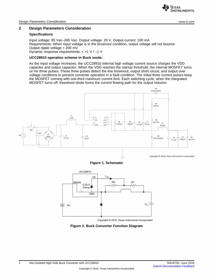
2 Design Parameters ConsiderationSpecificationsInput voltage: 85 Vac–265 Vac. Output voltage: 20 V, Output current: 100 mARequirements: When input voltage is in the brownout condition, output voltage will not bounce.Output ripple voltage < 200 mVDynamic response requirements: < +1 V / –1 V
UCC28910 operation scheme in Buck mode:As the input voltage increases, the UCC28910 internal high voltage current source charges the VDDcapacitor and output capacitor. When the VDD reaches the startup threshold, the internal MOSFET turnson for three pulses. These three pulses detect the line brownout, output short circuit, and output overvoltage conditions to prevent converter operation in a fault condition. The initial three current pulses keepthe MOSFET running with one-third maximum current limit. Each switching cycle, when the integratedMOSFET turns off, freewheel diode forms the current flowing path for the output inductor.
Figure 1. Schematic
Figure 2. Buck Converter Function Diagram

CCRpk
pk
VI
R=
2 3out VSR
2
R RV V
R
+
= ´
pkout
IV L
(1 D) T= ´
-
out
brownout
VD
V=
www.ti.com Design Parameters Consideration
3SNVA750–June 2016Submit Documentation Feedback
Copyright © 2016, Texas Instruments Incorporated
Non-Isolated High-Side Buck Converter with UCC28910
2.1 Output InductorConsidering the output inductor size and output capacitance, it is desired to set the controller switchingfrequency to 60 kHz. Discontinuous conduction mode (DCM) with valley switching is used to reduceswitching losses. Assuming the converter is working in the boundary conduction mode at lowest inputvoltage and highest load condition, the output inductor value is designed by the following equations:
where• Vbrownin = 72 V• Vbrownout = 43 V (1)
where• L = 290 µH (2)
To keep the converter working in DCM, TDK B82464P4224M000 is selected. The saturation current is0.75 A.
2.2 Output CapacitorOutput capacitance is a key factor to transient response, output voltage ripple, and system stability. Due tothe internal compensation of the UCC28910, the loop gain and phase cannot be obtained throughmeasurements. However, the load transient test can be used to verify the loop stability. After verification, a100-µF or more Aluminum capacitor is proved to allow stable operation.
2.3 VS pin: Divided ResistorsWhen MOSFET is off and inductor current comes to zero, the UCC28910 VS pin is used to detect theoutput voltage. Select the voltage divider ration to meet equation Equation 3:
where• VVSR = 4.05 V (3)
2.4 Startup ProcedureThrough internal integrated high voltage current source, the current source charges the VDD capacitorand output capacitor. When the VDD reaches the startup threshold, the internal MOSFET turns on forthree pulses. The controller sends out three pulses for detecting the UVLO, output short circuit, and outputovervoltage protection. The initial three current pulses keep in one-third maximum current limit.
2.5 Current LimitUse Equation 4 to calculate the current limit.
where• VCCR = 540 V (4)
To avoid the noise interference, the Ipk pin is preferred to be shorted to GND of the chip.
brownout VSL(stop) 2 outV I R V= ´ +
brownin VSL(run) 2V I R= ´
( )22out1 2 min p p
P 1(t t ) C V V V
eff 2
é ù+ = - - Dê úë û
Vp Vbulk
∆V
t1 t2
Design Parameters Consideration www.ti.com
4 SNVA750–June 2016Submit Documentation Feedback
Copyright © 2016, Texas Instruments Incorporated
Non-Isolated High-Side Buck Converter with UCC28910
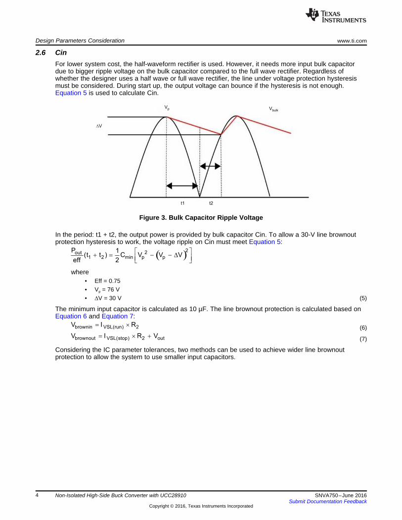
2.6 CinFor lower system cost, the half-waveform rectifier is used. However, it needs more input bulk capacitordue to bigger ripple voltage on the bulk capacitor compared to the full wave rectifier. Regardless ofwhether the designer uses a half wave or full wave rectifier, the line under voltage protection hysteresismust be considered. During start up, the output voltage can bounce if the hysteresis is not enough.Equation 5 is used to calculate Cin.
Figure 3. Bulk Capacitor Ripple Voltage
In the period: t1 + t2, the output power is provided by bulk capacitor Cin. To allow a 30-V line brownoutprotection hysteresis to work, the voltage ripple on Cin must meet Equation 5:
where• Eff = 0.75• Vp = 76 V• ∆V = 30 V (5)
The minimum input capacitor is calculated as 10 µF. The line brownout protection is calculated based onEquation 6 and Equation 7:
(6)
(7)
Considering the IC parameter tolerances, two methods can be used to achieve wider line brownoutprotection to allow the system to use smaller input capacitors.
2 3 5out VSR
3 5
R R / /RV V
R / /R
+
= ´
( )outbrownout VSL(stop) 2 5
2
VV I R / /R
R
æ ö= + ´ç ÷
è ø
( )brownin VSL(run) 2 5V I R / /R= ´
RF1
ACR1
20.0 kQ
L2
220 µH
C7
47 µF
D2
US1G-E3/5AT
D3
US1G-E3/5AT
C4
0.1 µF
C1
0.1 µF
R3
84.5 kQ
R2
336 kQ
L1
1 mH
C3
100 µF
C2
10 µF
C6
0.1 µF
R4
1.30 kQ
C8
100 pF
VS5
VDD6
8DRAN
IPK
GND
GND
GND
4
3
2
1
D1
RH06
RV1
R5
336 kQ
Copyright © 2016, Texas Instruments Incorporated
www.ti.com Design Parameters Consideration
5SNVA750–June 2016Submit Documentation Feedback
Copyright © 2016, Texas Instruments Incorporated
Non-Isolated High-Side Buck Converter with UCC28910
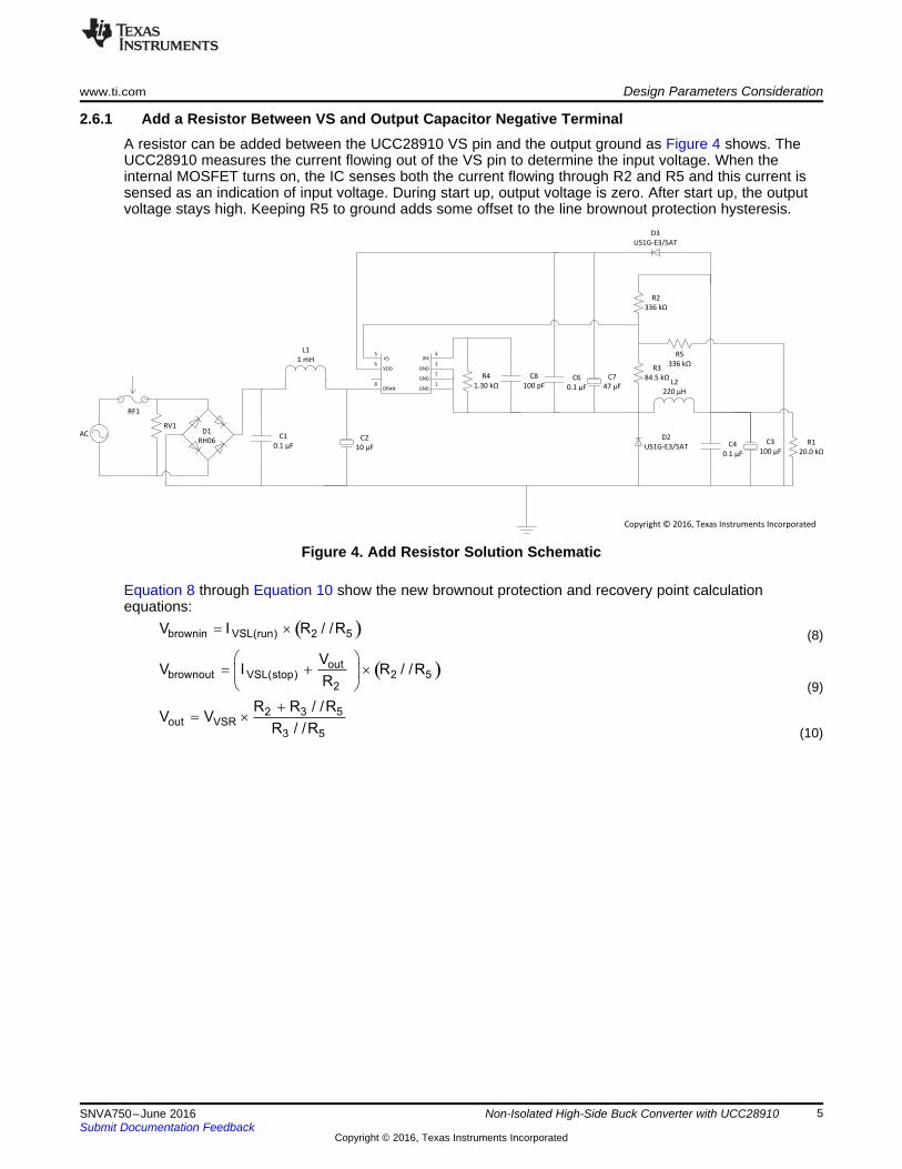
2.6.1 Add a Resistor Between VS and Output Capacitor Negative TerminalA resistor can be added between the UCC28910 VS pin and the output ground as Figure 4 shows. TheUCC28910 measures the current flowing out of the VS pin to determine the input voltage. When theinternal MOSFET turns on, the IC senses both the current flowing through R2 and R5 and this current issensed as an indication of input voltage. During start up, output voltage is zero. After start up, the outputvoltage stays high. Keeping R5 to ground adds some offset to the line brownout protection hysteresis.
Figure 4. Add Resistor Solution Schematic
Equation 8 through Equation 10 show the new brownout protection and recovery point calculationequations:
(8)
(9)
(10)
( )brownout VSL(stop) 2 5V I R R= ´ +
( )brownin VSL(run) 2 5V I R R= ´ +
RF1
ACR1
20.0 lQ
L2
220 µH
C7
47 µF
D2
US1G-E3/5AT
D3
US1G-E3/5AT
C4
0.1 µF
C1
0.1 µF
R3
84.5 lQ
R2
336 lQ
L1
1 mH
C3
100 µF
C2
10 µF
C6
0.1 µF
R4
1.30 lQ
C8
100 pF
VS5
VDD6
8DRAN
IPK
GND
GND
GND
4
3
2
1
D1
RH06
RV1
R5
336 lQ
D4
US1G-E3/5AT
Copyright © 2016, Texas Instruments Incorporated
Design Parameters Consideration www.ti.com
6 SNVA750–June 2016Submit Documentation Feedback
Copyright © 2016, Texas Instruments Incorporated
Non-Isolated High-Side Buck Converter with UCC28910
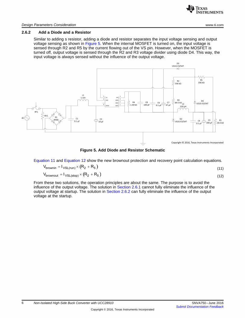
2.6.2 Add a Diode and a ResistorSimilar to adding s resistor, adding a diode and resistor separates the input voltage sensing and outputvoltage sensing as shown in Figure 5. When the internal MOSFET is turned on, the input voltage issensed through R2 and R5 by the current flowing out of the VS pin. However, when the MOSFET isturned off, output voltage is sensed through the R2 and R3 voltage divider using diode D4. This way, theinput voltage is always sensed without the influence of the output voltage.
Figure 5. Add Diode and Resistor Schematic
Equation 11 and Equation 12 show the new brownout protection and recovery point calculation equations.
(11)
(12)
From these two solutions, the operation principles are about the same. The purpose is to avoid theinfluence of the output voltage. The solution in Section 2.6.1 cannot fully eliminate the influence of theoutput voltage at startup. The solution in Section 2.6.2 can fully eliminate the influence of the outputvoltage at the startup.

Load (mA)Input Voltage (V)
30 mA
100 mA
10 mA
50 mA
230 V115 V
Eff
icie
ncy
Eff
icie
ncy
www.ti.com Test Result Waveform
7SNVA750–June 2016Submit Documentation Feedback
Copyright © 2016, Texas Instruments Incorporated
Non-Isolated High-Side Buck Converter with UCC28910
3 Test Result Waveform
3.1 MOSFET StressDue to the Buck configuration, the MOSFET voltage stress is about the same as input voltage. No voltagespike is observed. Figure 6 illustrates MOSFET voltage stress.
Figure 6. MOSFET Voltage Stress
3.2 EfficiencyDue to the nature of low duty cycle, the Buck converter is not able to achieve very high efficiency.However, the simple topology and few-external components still make it an attractive solution for certainapplications. Figure 7 illustrates comparisons in efficiency.
Figure 7. Efficiency Comparison
Test Result Waveform www.ti.com
8 SNVA750–June 2016Submit Documentation Feedback
Copyright © 2016, Texas Instruments Incorporated
Non-Isolated High-Side Buck Converter with UCC28910
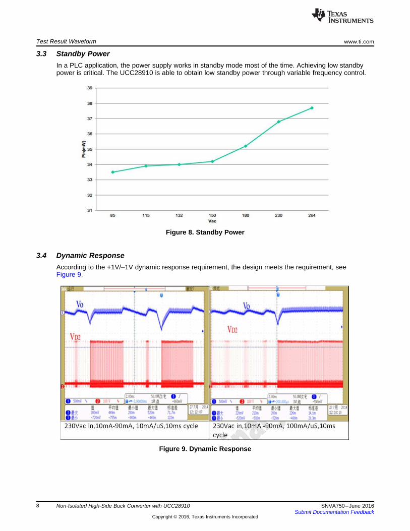
3.3 Standby PowerIn a PLC application, the power supply works in standby mode most of the time. Achieving low standbypower is critical. The UCC28910 is able to obtain low standby power through variable frequency control.
Figure 8. Standby Power
3.4 Dynamic ResponseAccording to the +1V/–1V dynamic response requirement, the design meets the requirement, seeFigure 9.
Figure 9. Dynamic Response
www.ti.com Test Result Waveform
9SNVA750–June 2016Submit Documentation Feedback
Copyright © 2016, Texas Instruments Incorporated
Non-Isolated High-Side Buck Converter with UCC28910
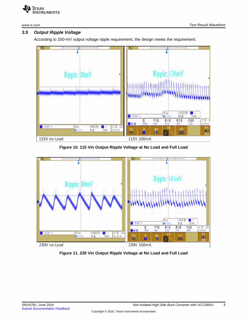
3.5 Output Ripple VoltageAccording to 200-mV output voltage ripple requirement, the design meets the requirement.
Figure 10. 115 Vin Output Ripple Voltage at No Load and Full Load
Figure 11. 230 Vin Output Ripple Voltage at No Load and Full Load

Test Result Waveform www.ti.com
10 SNVA750–June 2016Submit Documentation Feedback
Copyright © 2016, Texas Instruments Incorporated
Non-Isolated High-Side Buck Converter with UCC28910
3.6 Thermal Test at 25°CAccording to the 45° temperature rise requirement, the design meets the requirement.
Figure 12. 85 Vin Thermal Performance
Figure 13. 230 Vin Thermal Performance

www.ti.com Test Result Waveform
11SNVA750–June 2016Submit Documentation Feedback
Copyright © 2016, Texas Instruments Incorporated
Non-Isolated High-Side Buck Converter with UCC28910
3.7 EMI TestAccording to the EN55022B EMI limit, the design meets the requirement. Note: Output is not grounded.
Figure 14. 230 Vin EMI Performance
Figure 15. 115 Vin EMI Performance

Layout Suggestion www.ti.com
12 SNVA750–June 2016Submit Documentation Feedback
Copyright © 2016, Texas Instruments Incorporated
Non-Isolated High-Side Buck Converter with UCC28910
4 Layout SuggestionTo increase the reliability and feasibility of the design, TI recommends the layout uses the followingguidelines:1. Place the Ripk resistor as close as possible to the UCC28910 with the shortest traces possible.2. Try to minimize the area of DRAIN trace, this helps keep EMI disturbance low.3. A copper area connected to the GND pins improves heat sinking thermal performance.4. Place the auxiliary voltage sense resistor divider directly on the VS pin keeping traces as short as
possible.
5 ConclusionThrough test and optimization, the non-isolated Buck converter achieves the performance meeting thespecifications. This paper also details two methods for improving the hysteresis for line brownoutprotection. EMI standard EN55022B is also compliant. The non-isolated Buck converter is suitable forindustrial and appliance applications.
6 Reference1. UCC28910: High-Voltage, Flyback Switcher with Primary-Side Regulation and Output Current Control
(SLUS769)2. PMP4443: Universal AC input, 20V/100mA Non-isolated High-side Buck Converter

IMPORTANT NOTICE
Texas Instruments Incorporated and its subsidiaries (TI) reserve the right to make corrections, enhancements, improvements and otherchanges to its semiconductor products and services per JESD46, latest issue, and to discontinue any product or service per JESD48, latestissue. Buyers should obtain the latest relevant information before placing orders and should verify that such information is current andcomplete. All semiconductor products (also referred to herein as “components”) are sold subject to TI’s terms and conditions of salesupplied at the time of order acknowledgment.TI warrants performance of its components to the specifications applicable at the time of sale, in accordance with the warranty in TI’s termsand conditions of sale of semiconductor products. Testing and other quality control techniques are used to the extent TI deems necessaryto support this warranty. Except where mandated by applicable law, testing of all parameters of each component is not necessarilyperformed.TI assumes no liability for applications assistance or the design of Buyers’ products. Buyers are responsible for their products andapplications using TI components. To minimize the risks associated with Buyers’ products and applications, Buyers should provideadequate design and operating safeguards.TI does not warrant or represent that any license, either express or implied, is granted under any patent right, copyright, mask work right, orother intellectual property right relating to any combination, machine, or process in which TI components or services are used. Informationpublished by TI regarding third-party products or services does not constitute a license to use such products or services or a warranty orendorsement thereof. Use of such information may require a license from a third party under the patents or other intellectual property of thethird party, or a license from TI under the patents or other intellectual property of TI.Reproduction of significant portions of TI information in TI data books or data sheets is permissible only if reproduction is without alterationand is accompanied by all associated warranties, conditions, limitations, and notices. TI is not responsible or liable for such altereddocumentation. Information of third parties may be subject to additional restrictions.Resale of TI components or services with statements different from or beyond the parameters stated by TI for that component or servicevoids all express and any implied warranties for the associated TI component or service and is an unfair and deceptive business practice.TI is not responsible or liable for any such statements.Buyer acknowledges and agrees that it is solely responsible for compliance with all legal, regulatory and safety-related requirementsconcerning its products, and any use of TI components in its applications, notwithstanding any applications-related information or supportthat may be provided by TI. Buyer represents and agrees that it has all the necessary expertise to create and implement safeguards whichanticipate dangerous consequences of failures, monitor failures and their consequences, lessen the likelihood of failures that might causeharm and take appropriate remedial actions. Buyer will fully indemnify TI and its representatives against any damages arising out of the useof any TI components in safety-critical applications.In some cases, TI components may be promoted specifically to facilitate safety-related applications. With such components, TI’s goal is tohelp enable customers to design and create their own end-product solutions that meet applicable functional safety standards andrequirements. Nonetheless, such components are subject to these terms.No TI components are authorized for use in FDA Class III (or similar life-critical medical equipment) unless authorized officers of the partieshave executed a special agreement specifically governing such use.Only those TI components which TI has specifically designated as military grade or “enhanced plastic” are designed and intended for use inmilitary/aerospace applications or environments. Buyer acknowledges and agrees that any military or aerospace use of TI componentswhich have not been so designated is solely at the Buyer's risk, and that Buyer is solely responsible for compliance with all legal andregulatory requirements in connection with such use.TI has specifically designated certain components as meeting ISO/TS16949 requirements, mainly for automotive use. In any case of use ofnon-designated products, TI will not be responsible for any failure to meet ISO/TS16949.
Products ApplicationsAudio www.ti.com/audio Automotive and Transportation www.ti.com/automotiveAmplifiers amplifier.ti.com Communications and Telecom www.ti.com/communicationsData Converters dataconverter.ti.com Computers and Peripherals www.ti.com/computersDLP® Products www.dlp.com Consumer Electronics www.ti.com/consumer-appsDSP dsp.ti.com Energy and Lighting www.ti.com/energyClocks and Timers www.ti.com/clocks Industrial www.ti.com/industrialInterface interface.ti.com Medical www.ti.com/medicalLogic logic.ti.com Security www.ti.com/securityPower Mgmt power.ti.com Space, Avionics and Defense www.ti.com/space-avionics-defenseMicrocontrollers microcontroller.ti.com Video and Imaging www.ti.com/videoRFID www.ti-rfid.comOMAP Applications Processors www.ti.com/omap TI E2E Community e2e.ti.comWireless Connectivity www.ti.com/wirelessconnectivity
Mailing Address: Texas Instruments, Post Office Box 655303, Dallas, Texas 75265Copyright © 2016, Texas Instruments Incorporated