no. 2d730-i 36e*c diagnostic function manual for model … · no. 2d730-i 36e*c diagnostic function...
TRANSCRIPT

No. 2D730-I 36E*C
DIAGNOSTIC FUNCTION MANUAL
FOR
MODEL SSA-340A
SERVICE TEST SYSTEM
(ZD730=136E*C)
TOSHIBA CORPORATION
@ TOSHIBA CORPORATION 1995
ALL RIGHTS RESERVED

No. 2D730-136E*C
REVISION RECORD
REV. DATE REASON PAGE SER. DOC. (hlAliYY) /AUTHOR CHANGED No. PRODUCT.
INI. 02/'95 Mr. Nakajima -_----- TM-WW
*A 111'95 121'95 upgrade is supported. P. 4-113 to Mr. Yamazaki 115
"B lo/'96 121'96 upgrade is supported. Mr. Okumoto
"C 071'98 101'98 upgrade is supported. Mr. Okumoto
R-l *

No. 2D730-136E
CONTENTS
1.
2.
3.
INTRODUCTION ____________________------- ____________________~~~~~~~~ l-l
OUTLINE OF THE TEST SYST~_~~~_____~~~~~__~~~~~~~~~~~~~~~~~~~~~~~~~2~1
2.1 Configuration of the Test System ____________________~~~~~~~~~~ 2-l
2.2 Diagnostic Items and Nature of Tests in the Test System-------2-l
2.3 Test Modes (ALL, SUB) -------------- ____________________------- 2-12
TROUBLESHOOTING _______~____~~~~___~~~~~_~~~~~~~~~~~~~~~~~~~~~~____~3~1
3.1 Preparatory Work --------------- ____________________~~~~~~~~~~~ 3-3
3.2 Operating Precautions for the Test Systems --------------------3-3
3.3 Operating Procedure ___~~~~__~~~~~~~~~~~~~~~~~~~~~~~~~~~~~~_~~~3~4
3.3.1 Procedure until the menu message is displayed ----------3-4
3.3.2 Flowchart of the ALL mode ~~~~~~~~~~~~~~~~~~~~~~~~~~__~~3~6
3.3.3 Flowchart of the SUB mode ~~~~_~~~~~~~~~~~~~~~~~~~~~___~3~6
3.3.4 Command ___________________________--____----___~~~~____3_S
3.3.5 Changing the frequency of test execution---------------3-10
3.4 Error Code Table ______~~~~_~~~~~~~~~~~~~~~~~~~~~~~~~~~~~~~~~~~3~13
4. FLOWCHARTS FOR IDENTIFYING MALFUNCTIONS ____________________~~~~~~~~ 4-l
Page
4.1 Identifying Faults in the CPU Unit _______________--___~~~~~~~~ 4-l
4.1.1 Preparatory work________~_____~~~~~_~~~~~~_______~_____4~~
4.1.2 Flowchart for identifying malfunctions -----------------4-l
4.1.3 Decision criteria____~~~~_-__~~~~~~~~~~~~~_~_~~~~~_~~~~4~3
4.1.4 Supplement----------- ____________________~~~~~~~~~~~~~~ 4-13
4.2 Identifying Faults in the PANEL Unit ____________________------ 4-13
4.2.1 Preparatory work_~_______~___~_~--~~---------------~~~-4-13
4.2.2 Flowchart for identifying faults -----------------------4-13
4.2.3 Criteria ____________________~~~~~~~~~~~~~~~~~~~~~~~~~~~ 4-14
4.2.4 Sunnlement ____________________~~~~~~~~~~~~~~~~~~~~~~~~~ 4-16
-a-

No. 2D730-136E
CONTENTS - continued
Page
4.3 Identifying Faults in RPG ____________________~~~~~~~~~~~~~~~~~ 4-18
4.3.1 Preparatory work ____________________~~~~~~~~~~~~~~~~~~~ 4-18
4.3.2 Troubleshooting flowchart ____________________~~~~~~~~~~ 4-18
4.3.3 Decision tree ______-__-__________~~~~~~~~~~~~~~~~~~~~~~ 4-20
4.3.4 Supplement _________-__________~~~~~~~~~~~~~~~~~~~~~~~~~ 4-21
4.4 Identifying Faults in the DSC Unit ____________________~~~~~~~~ 4-23
4.4.1 Preparations _______-____________~~~~~~~~~~~~~~~~~~~~~~~ 4-23
4.4.2 Troubleshooting flowchart------------------------------4-23
4.4.3 Criteria ____________________~~~~~~~~~~~~~~~~~~~~~~~~~~~ 4-25
4.5 Identifying Faults in the T/R Unit----------------------------4-56
4.5.1 Preparations _______-____________~~~~~~~~~~~~~~~~~~~ ____4_56
4.5.2 Fault diagnosis flow chart ____________________~~~~~~~~~ 4-56
4.5.3 Criteria ____________________~-~~~~~~~~~~~~~~~~~~~~~~~~~ 4-59
4.5.4 Supplement ____________________~~~~~~~~~~~~~~~~~~~~~~~~~ 4-71
4.6 Identifying Faults in the FFT Unit----------------------------4-76
4.6.1 Preparatory work ____________________~~~~~~~~~~~~~~~ --m-4-76
4.6.2 Flowchart for identifying faults -----------------------4-76
4.6.3 Criteria ____________________~~~~~~~~~~~~~~~~~~~~~~~~~~~ 4-79
4.6.4 Supplement ~~~~~~~~~~___~__~~~~~~~~~~~__~~~~~~~~~_~~~~~~4~~~
4.7 Identifying Faults in the CFM Unit ----------------------------4-87
4.7.1 Preparatory work_~_~________~~~~~_~~~______~~~_____~~~~4~87
4.7.2 Flowchart for identifying faults -----------------------4-87
4.7.3
4.7.4 Results of the diagnostic tests ------------------------4-105
4.7.5 Supplement ____________________~~~~~~~~~~~~~~~~~~~~~ ----4-111
4.8 Maintenance ____________________~~~~~~~~~~~~~~~~~~~~~~~~~~~~~~~ 4-113
-b-

No. 2D730-136E
CONTENTS - continued
Page
5. APPENDIX ____________________~~~~~~~~~~~~~~~~~~~~~~~~~~~~~~~-~~~~~~~ 5-1
5.1 Error Codes for Self-diagnosis ___-________________~~~~~~~~~~~~ 5-1
5.2 Patch Menu Operation ____________________~~~~~~~~~~~~~~~~~~~~~~ 5-5 <.
5.2.1 Applicable equipment ____________________~~~~~~~~~~~~~~~ 5-5
5.2.2 Starting ____________________~~~~~~~~~~~~~~~~~~~~~~~~~~~ 5-5
5.2.3 Memory R/W & dump ____________________~~~~~~~~~~~~~~~~~~ 5-6
5.2.4 Coordinate check (X,Y) ____________________~~~~~~~~~~~~~ 5-7
5.2.5 Image cant external value set ____________________------ 5-7
5.2.6 Address & data value save ______________________________5_g
- c -

No. 2D730-136E
1. INTRODUCTION
Test systems are service test units for the ultrasonic diagnostic equipment model SSA-340A.
This manual explains the diagnostic procedures.
Furthermore, since certain PWBs can be checked only if the system
operates normally, it is necessary to perform testing in the following
order.
(1) CPU unit
(2) RPG
(3) DSC unit
(4) T/R unit
(5) FFT unit
(6) CFM unit
(7) PANEL unit
l-1

No. 2D730-136E
2. OUTLINE OF THE TEST SYSTEM
If a malfunction occurs, the test system will indicate the test results with respect to PWBs and PWB blocks, identifying those which are
responsible for the malfunction by displaying error codes. Alternately,
the test system will indicate a pattern which permits assessment of the quality of each block.
Tests principally involve the CPU unit, PANEL unit, RPG, DSC unit, T/R ;2-----_
unit, FFT unit, and CFM unit. Although not all units are included, it is possible to test the basic units required for generating an image. Therefore, troubleshooting is expedited if the test system succeeds in helping identify faulty units.
Furthermore, at the time of maintenance and checking it is possible to assess changes in ultrasonic wave transmission which-are difficult to observe during- the normal service period; degradation of system performance; and memory errors of any addresses caused by faulty reception.
In addition, there are guidelines for test performance frequency. This
is useful for checking faults that occur infrequently, caused by RS-232C communication errors.
2.1 Configuration of the Test System
This test system is incorporated in the main unit of the diagnostic ultrasound system.
This manual describes the operating procedures for the test system.
2.2 Diagnostic Items and-Nature of Tests in the Test System
PWBs which are tested by the test system are shown in figure 2-1 to figure 2-3. Details concerning each test item are given in tables 2-1 and 2-2.
2-l

No. 2D730-136E

No. 2D730-136E
Table 2-1 Table of equipment and corresponding test items
0 : Function available x: Function not available
Execution Unit under seauence test
Check item SSA-340A
3 GRAPHIC MEMORY CHECK 0
4 RS-232C CHl CHECK 0
5 RS-232C CH2 CHECK X
6 CENTRONICS CHECK X
7 PANEL unit LED CHECK 0
8 I ~ RPG T RATE CHECK I 0
-4 DSC unit 1 B/W FM CPU R/W I 0
r- ~~ B/W TEST PATTERN (SYNC) I_ 0
1 B/W TEST PATTERN (ASYNC) 1 o
I B/W LIP TEST PATTERN I COLOR FM CPU R/W I CAL TEST PATTERN (R)
1 CAL TEST PATTERN (THETA) ) o
I COLOR RIP TEST PATTERN I 0
I COLOR LIP TEST PATTERN I 0
T/R unit 1 T/R CONT RAM CHECK I 0
DELAY CONT RAM CHECK 0
R-CHANNEL CHECK (SECTOR) X
1 R-CHANNEL CHECK (CONVEX) 1 o
1 T-CHANNEL CHECK (CONVEX) 1 o
1 DELAY TIME CHECK (CONVEX) 1 o
I PH.D OSC CHECK I 0 24 FFT unit
25
26
27
28 CFM unit
I FORWARD FLOW CHECK I 0
I REVERSE FLOW CHECK I 0
29 I 30 I
31 I 1 LB/FIL/CORR/CAL SELF TEST 1 o
32 LB/CAL CHECK 0
33 LB/FIL/CORR/CAL CHECK 0
2-3

Table 2-2 Table of test items
Execu- tion se- quence
1
2
3
4
Unit under test
CPU unit
Check item
CPU RAM R/W CHECK
CPU ROM CHECK
GRAPHIC MEMORY CHECK
RS-232C CHl CHECK
Purpose of test (nature of check)
Confirmation of RAM operation in the CPU program [The CPU writes data in RAM and then reads the same data. It then checks RAM function by comparing the two sets of data.]
Confirmation of ROM operation in the CPU program [ROM data are added and compared with data added and stored previously. The system checks ROM operation by comparing the two sets of data.]
Confirmation of memory operation for display of characters and graphics [The CPU fills the entire memory with alternating l's and O's, thus filling the screen with entirely white and entirely black areas.] (When color is used, blue and green are also displayed.)
Checking of RS-232C transmission and reception for CHl [Transmitted data are received unchanged, and compared.]
Message displayed (error code)
Normal: 'OK"
Abnormal: Display of abnormal RAM address
Normal: 11 OK II
Abnormal: Display of abnormal RAM address
Normal: A black and white (green and blue) pattern is seen over the entire screen. .
Abnormal: Dot-like and line artifacts are seen.
Normal: ” OK "
Abnormal: Display of error type
Judge- ment
Remarks
CPU
CPU
Service engineer
CPU Loopback CNN is required.
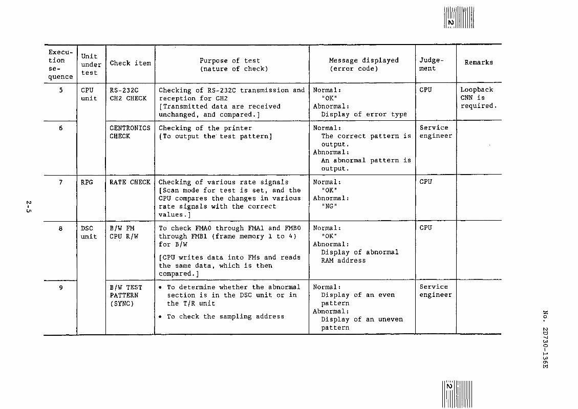
Execu- tion se- quence
5
Unit under test
CPU unit
Message displayed (error code)
Judge- ment
Purpose of test (nature of check)
Checking of RS-232C transmission and reception for CH2 [Transmitted data are received unchanged, and compared.]
Remarks Check item
CPU Loopback CNN is required.
RS-232C CH2 CHECK
Normal: "OK"
Abnormal: Display of error type
Normal: The correct pattern is output.
Abnormal: An abnormal pattern is output.
Service engineer
6 CENTRONICS CHECK
Checking of the printer [To output the’ test pattern]
Normal: t1 OK II
Abnormal: "NG"
CPU 7 RPG RATE CHECK Checking of various rate signals [Scan mode for test is set, and the CPU compares the changes in various rate signals with the correct values.]
To check FMAO through FMAl and FMBO through FMBl (frame memory 1 to 4) for B/W
[CPU writes data into FMs and reads the same data, which is then compared.]
CPU 8 DSC unit
B/W FM CPU R/W
Normal: "OK"
Abnormal: Display of abnormal RAM address
l To determine whether the abnormal section is in the DSC unit or in the T/R unit
l To check the sampling address
Normal: Display of an even pattern
Abnormal: Display of an uneven pattern
9 Service engineer
B/W TEST PATTERN (SYNC)

Execu- tion se- quence
10
11
tu
b 12
13
Unit under test
DSC unit
Check item
B/W TEST PATTERN (ASYNC)
B/W LIP TEST PATTERN
COLOR FM CPU R/W
CAL TEST PATTERN
(R)
Purpose of test (nature of check)
l To determine whether the abnormal section is in the DSC unit or in the T/R unit
l To check the multistage transmission
To determine whether the abnormality is before the output section or after in the DSC unit [The test pattern is input in the linear interpolation circuit.]
To check FMAO through FM2 and FMBO through FM82 (frame memory 1 to 6) for COLOR [CPU writes data into FMs and reads the same data, which is then compared.]
l To check the interpolation function (RIP) in the DSC unit
l To determine whether the abnormality is in the MT1 unit or in the DSC unit
[Interpolation check in the DSC r-direction and threshold check in
the e-direction]
(RIP: Radius direction interpolation)
Message displayed (error code)
Normal: Display of an even pattern
Abnormal: Display of an uneven pattern
Normal: Display of a pattern of the interpolated vertical lines
Abnormal: Display of an abnormally interpolated pattern.
Normal: ” OK ”
Abnormal: Display of abnormal RAM address
Normal: Display of an even pattern interpolated in the r-direction
Abnormal: Display of an abnormally interpolated pattern
Judge- ment
Service engineer
Service engineer
CPU
Service engineer
Remarks

Execu- tion se- quence
14
15
16
17
Unit under test
DSC unit
T/R unit
Check item
CAL TEST PATTERN (THETA)
COLOR RIP TEST PATTERN
COLOR LIP TEST PATTERN
T/R CONT RAM CHECK
Purpose of test (nature of check)
l To check the interpolation function (WIP) in the DSC unit
l To determine whether the abnormal portion is the MT1 unit or in the DSC unit
[Interpolation check in the DSC r-direction and threshold check in the 8-direction]
(WIP: Write interpolation)
To determine whether the abnormal section is before or after the input system of the DSC system. (Identifying the abnormality between the MT1 unit and in the DSC unit)
[The test pattern is input in the RIP circuit.]
To determine whether the abnormality is in the section before the output section of the DSC unit or after
[The test pattern is input to the linear interpolation circuit.]
To confirm COMMAND RAM operation [The CPU writes data into COMMAND RAM, and reads the same data, then performs checking by comparing the two.]
Message displayed (error code)
Normal: Display of an even pattern interploated in the U-direction
Abnormal: Display of an abnormally interpolated pattern
Normal: Display of an interpolated pattern
Abnormal: Display of an abnormally interpolated pattern
Normal: Display of a pattern of interpolated vertical lines
Abnormal: Display of an abnormally interpolated pattern
Normal: "OK"
Abnormal: Display of abnormal address in RAM
Judge- ment
Service engineer
Service engineer
Service engineer
CPU
Remarks

Execu- tion se- quence
18
19
20
21
22
Unit under test
T/R unit
Check item
DELAY CONT RAM CHECK
R-CHANNEL CHECK (RESERVE)
R-CHANNEL CHECK (CONVEX)
T-CHANNEL CHECK (CONVEX)
DELAY TIME CHECK (CONVEX)
Purpose of test (nature of check)
To confirm BRI RAM operation [The CPU writes data into BRI RAM, and reads the same data, then performs checking by comparing the two.]
To confirm that each channel of R- DELAY in the CONVEX system is receiving correctly [Transmission is made by multiple channels, and is sequentially received by one channel at a time for each rate, thus constructing an image.]
To confirm that each channel of PULSER is transmitting correctly (Transmission is made sequentially by one channel at a time for each rate, thus constructing an image.]
To confirm that the delay time in transmission system is controlled correctly [Pattern resulting from the initial echo is to be continuous without any differences in level. (It should be checked comparing the pattern resulting from the CPU.)]
Message displayed (error code)
Normal: "OK"
Abnormal: Display of abnormal address in RAM
Normal: No variations in brightness
Abnormal: Variations in brightness
Normal: No variation in brightness
Abnormal: Variations in brightness
Normal: Delay time pattern of continuous type
Abnormal: Pattern of non- continuous type
Judge- ment
CPU
Service engineer
Service engineer
Service engineer
Remarks

Execu- tion se- quence
23
24
25
N
\o
26
27
Unit under test
FFT
CFM
Check item
PH.D OSC CHECK
FORWARD FLOW CHECK
REVERSE FLOW CHECK
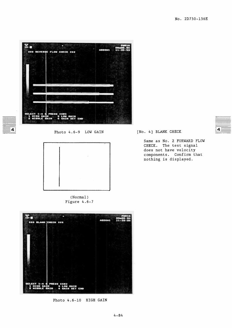
BLANK CHECK
LB SELF TEST
Purpose of test (nature of check)
Determining whether the abnormal portion is in the FFT or in the T/R system. [To send the test pattern to the PHASE DETECTION input]
To test for abnormalities following FFT [To send the sequential test pattern to the FFT input]
To test for abnormalities following FFT [To send the reverse test pattern to the FFT input]
Same as above [To send the non-signal test pattern to the FFT input]
The test pattern is input, and the results of operation are compared with the correct value. [To test only the test RAM of the line buffer]
Message displayed (error code)
Normal: Agress with the expected value pattern
Abnormal: Does not agree with the expected value pattern
Same as above
Normal: Agress with the expected value pattern
Abnormal: Does not agree with the expected value pattern
Normal: No message
Abnormal: Display of white points, etc.
Normal: II OK II
Abnormal: Display of error message
Judge- ment
Remarks
Service engineer
Service engineer
Service engineer
Service engineer
CPU
Execu- tion se- quence
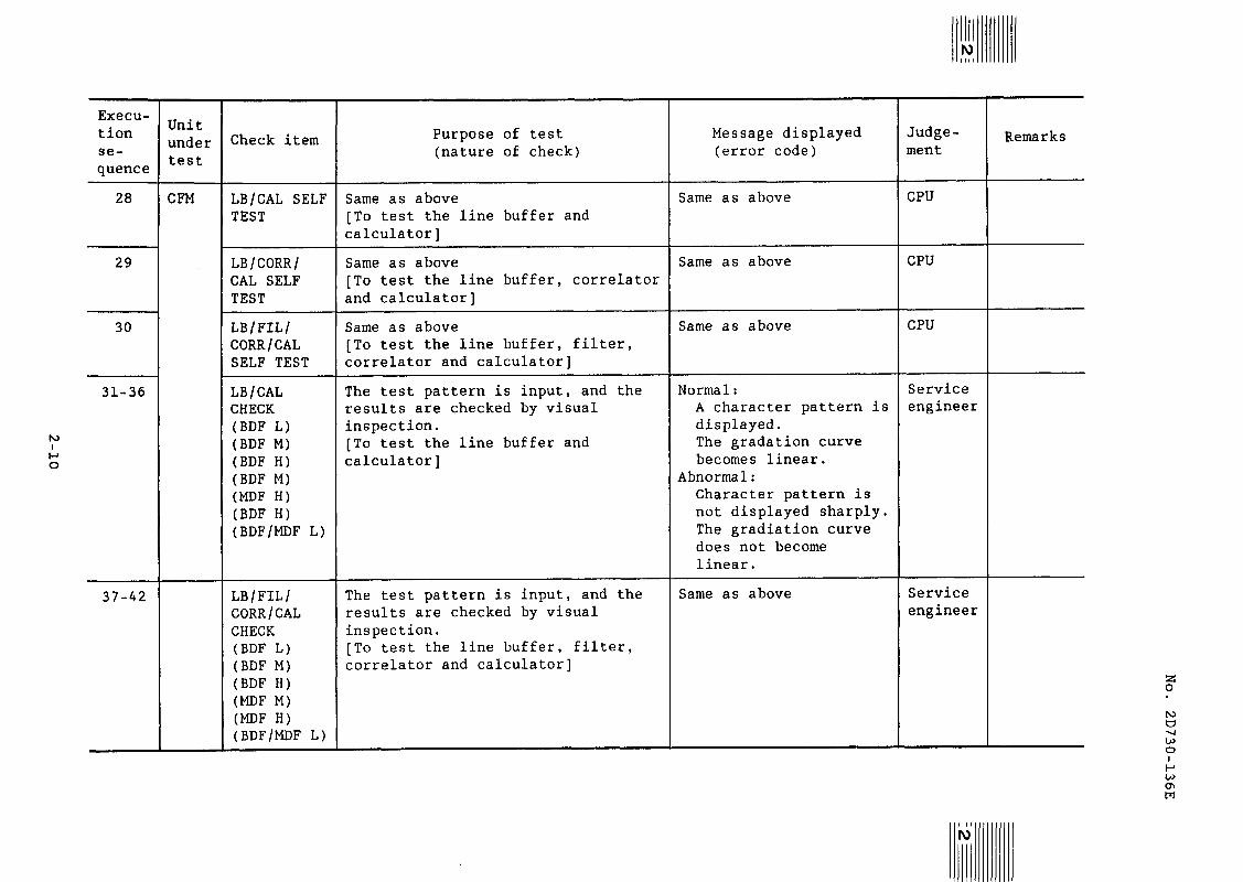
28
29
30
31-36
37-42
Unit under test
CFM
Check item
LB/CAL SELF TEST
LB/CORR/ CAL SELF TEST
LB/FIL/ CORR/CAL SELF TEST
LB/CAL CHECK (BDF L) (BDF M) (BDF H) (BDF M)
WDFH) (BDF H) (BDF/MDF L
LB/FIL/ CORR/CAL CHECK (BDF L) (BDF M) (BDF H)
WDFM) WFH) (BDF/MDF L)
Purpose of test (nature of check)
Same as above [To test the line buffer and calculator]
Same as above [To test the line buffer, correlator and calculator]
Same as above [To test the line buffer, filter, correlator and calculator]
The test pattern is input, and the results are checked by visual inspection. [To test the line buffer and calculator]
The test pattern is input, and the results are checked by visual inspection. [To test the line buffer, filter, correlator and calculator]
Message displayed (error code)
Same as above
Same as above
Same as above
Normal: A character pattern is displayed. The gradation curve becomes linear.
Abnormal: Character pattern is not displayed sharply. The gradiation curve does not become linear.
Same as above
Judge- ment
CPU
CPU
CPU
Service engineer
Service engineer
Remarks

No. 2D730-136E
2-11
No. 2D730-136E
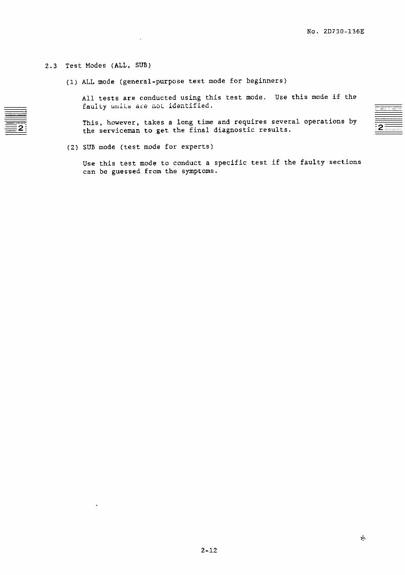
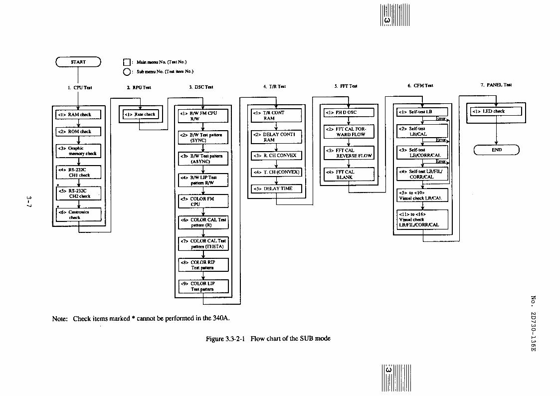
2.3 Test Modes (ALL, SUB)
(1) ALL mode (general-purpose test mode for beginners)
All tests are conducted using this test mode. Use this mode if the
faulty units are not identified.
This, however, takes a long time and requires several operations by the serviceman to get the final diagnostic results.
;2E
(2) SUB mode (test mode for experts)
Use this test mode to conduct a specific test if the faulty sections can be guessed from the symptoms.
2-12

No. 2D730-136E
3. TROUBLESHOOTING
Carry out tests to identify malfunctions according to the following procedure:
(1) Preliminary survey
(2) Preparatory work (with the power off)
(3) Setting of the service mode
(4) Setting of the test mode (ALL, SUB mode)_
(5) Test
*(6) Identification of malfunction based on the error code table
Figure 3-l shows the flowchart for the above procedure.
Preliminary survey
Survey the stated problems not just by relying on information from the customer, but also by checking carefully the status of each mode and function. Problems that occur only occasionally cannot be identified by the test system when it is not actually occurring.
(For tests which are controlled by the CPU, such as the check of the RS- 232C or the R/W of MM, the test system can provide a means of reproducing the phenomenon by repeating the test sequence an unlimited number of times.)
3-1

No. 2D730-136E
(5 Preparatory work
J. , 4 . Rcfcrcncc manual for the test system
(This manual)
. Set of gcncral service tools l Jigs rcquircd Tar the test
I Prcparc tools, etc. t
. ..* . . . . .
1 . Connect the specified probe
(See section 3.2. (I)). l Set the B-GAIN to MAX. l Set the DEPTH to 10 cm.
3 Turn on the power.
to display the
SETTING menu
I Move the cursor to [SERVICE] in the SETTING menu and I
* : The proccdurcs for entering the SERVICE menu differ dcpcnding on the site. I 0 press I . 0
* i
_____-__---____ __________---- 1
___
__-
- At thus tlmc, the system enters the
Press @ , @ on the
keyboard. At this time, the system enters the SERVICE menu.
_________----- 1
Move the cursor to [TEST] in
the SERVICEmcnu and 1 /o/
.
At this time, WSTj is high- lighted and the TV screen changes to the screen for testing.
+ I t
Enter numbers (for example, [0] the keyboard.
@ ) from
I Carry out various tests. I (Carry)
I Error codes and messages will bc displayed. I
I Identify faulty PWBs using the error code table. I
Figure 3-1
3-2

No. 2D730-136E*C
3.1 Preparatory Work
Prepare the required tools/devices (such as a return connector) in accordance with the "Preparatory work" in section 4. (ex. LOOP BACK CNN)
3.2 Operating Precautions for the Test Systems
(1) Before carrying out tests, the transducer shold be connected as specified below. Do not pull out or connect a probe during the test unless so instructed, otherwise a malfunction may occur.
1 TRANSDUCER C ) TRANSDUCER B I TRANSDUCER A
SSA-340A No connection Linear or convex transducer, PVF-375MT or no connection
(2) A transient phenomenon is displayed while the test is being carried out; however, this is not abnormal.
(3) The time, heart rate, PWR value, ID area and hospital name are not erased. The ID indication is erased.
(4) Pressing (/LJI1 at the graphic check of the CPU may cause a blank area
on the upper right of the image; however, this is not abnormal (Photo 3.2-l).
(5) Although most switches are disabled during the serviceman test, do not press the following switches to avoid a malfunction:
l VCR SW (on the panel) l Palm controller trackball l Trackball (TRACK BALL FUNCTION)
(6) When the graphic check of the CPU is completed, either of the two lines for time display may not be displayed; however, this is not abnormal.
(7) Because peripheral devices may malfunction during testing, disconnect the control cables of all peripheral devices during testing. Alternatively, turn OFF the power of all peripheral devices.
(8) Be sure to execute New Patient after the test has been completed.
3-3

No. 2D730-136E
Photo 3.2-l
3.3 Operating Procedure
3.3.1 Procedure until the menu message is displayed
First perform the "Setting of the service mode" of the flowchart shown
in figure 3-1.
The screen shown in figure 3.3-l-l first appears in the serviceman test. Then the caution screen shown in photo 3.3-l-Z appears, requesting that the following be checked.
(1) The probes specified in section 3.2 (1) have been connected.
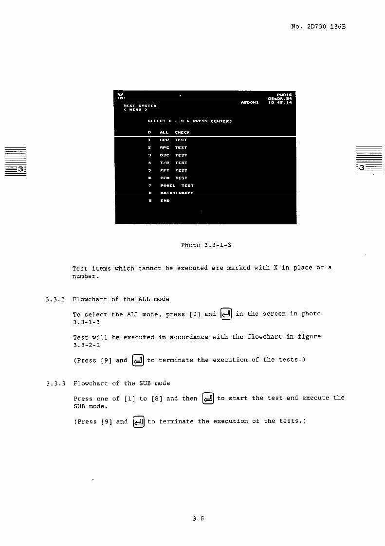
After confirming the above, press &J and the screen in photo 3.3-l-3 will appear.
0
3-4

Photo 3.3-l-l
No. 2D730-136E*B
Photo 3.3-l-Z
3-5
No. 2D730-136E
Photo 3.3-l-3
Test items which cannot be executed are marked with X in place of a number.
3.3.2 Flowchart of the ALL mode
To select the ALL mode, press [0] and 4 in the screen in photo 0 3.3-l-3
Test will be executed in accordance with the flowchart in figure 3.3-2-l
(Press [9] and mto terminate the execution of the tests.)
3.3.3 Flowchart of the SUB mode
Press one of Cl] to [8] and then 4 to start the test and execute the SUB mode.
U
(Press [9] and mto terminate the execution of the tests.)
3-6
No. 2D730-136E
1
_,I! 0
!!I A
ii 1
I
No. 2D730-136E
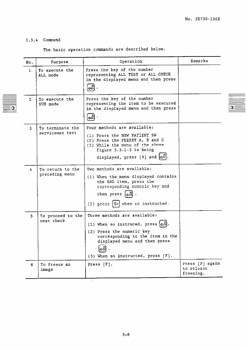
3.3.4 Cormnand
The basic operation commands are described below.
Remarks Purpose Operation No.
Press the key of the number representing ALL TEST or ALL CHECK
I
in the displayed menu and then press
1 :o execute the LLL mode
IO 4 .
Press the key of the number representing the item to be executed in the displayed menu and then press
2 Co execute the XJB mode
Four methods are available:
(1) Press the NEW PATIENT SW (2) Press the PRESET A, B and C (3) While the menu of the above
figure 3.3-l-3 is being
displayed, press [9] and 4. 0
3 To terminate the serviceman test ,
Two methods are available:
(1) When the menu displayed contains the END item, press the corresponding numeric key and
4 To return to the preceding menu
then press 141 .
(2) press + when so instructed. U Three methods are available: To proceed to the
next check 5
When so instruced, press 4. 0 Press the numeric key corresponding to the item in the displayed menu and then press
(1)
(2)
(3)
@I . When so instructed, press [F].
Press [P] again to release freezing.
Press [PI. 6 To freeze an image
3-8
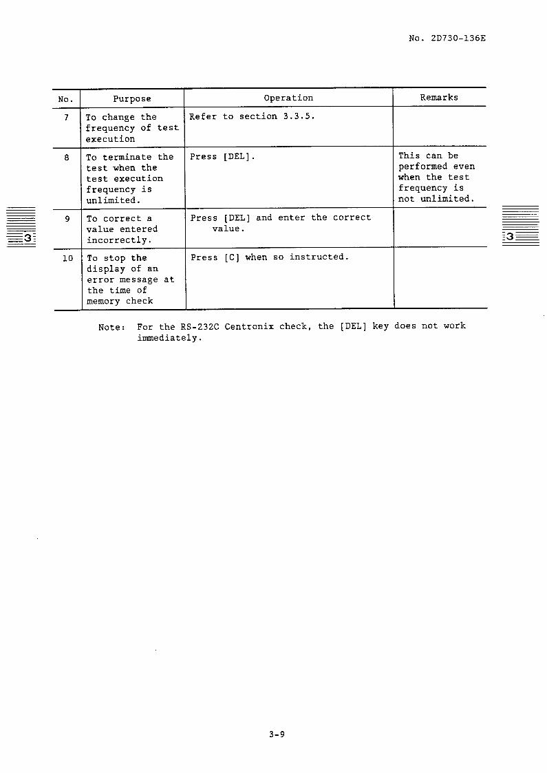
No. 2D730-136E
No.
7
8
9
10
Purpose
To change the frequency of test execution
To terminate the test when the test execution frequency is unlimited.
To correct a value entered incorrectly.
To stop the display of an error message at the time of memory check
Operation I Remarks
Refer to section 3.3.5.
Press [DEL]. This can be performed even when the test frequency is not unlimited.
Press [DEL] and enter the correct value. I
Press [C] when so instructed.
Note: For the RS-232C Centronix check, the [DEL] key does not work immediately.
3-9
No. 20730-136E
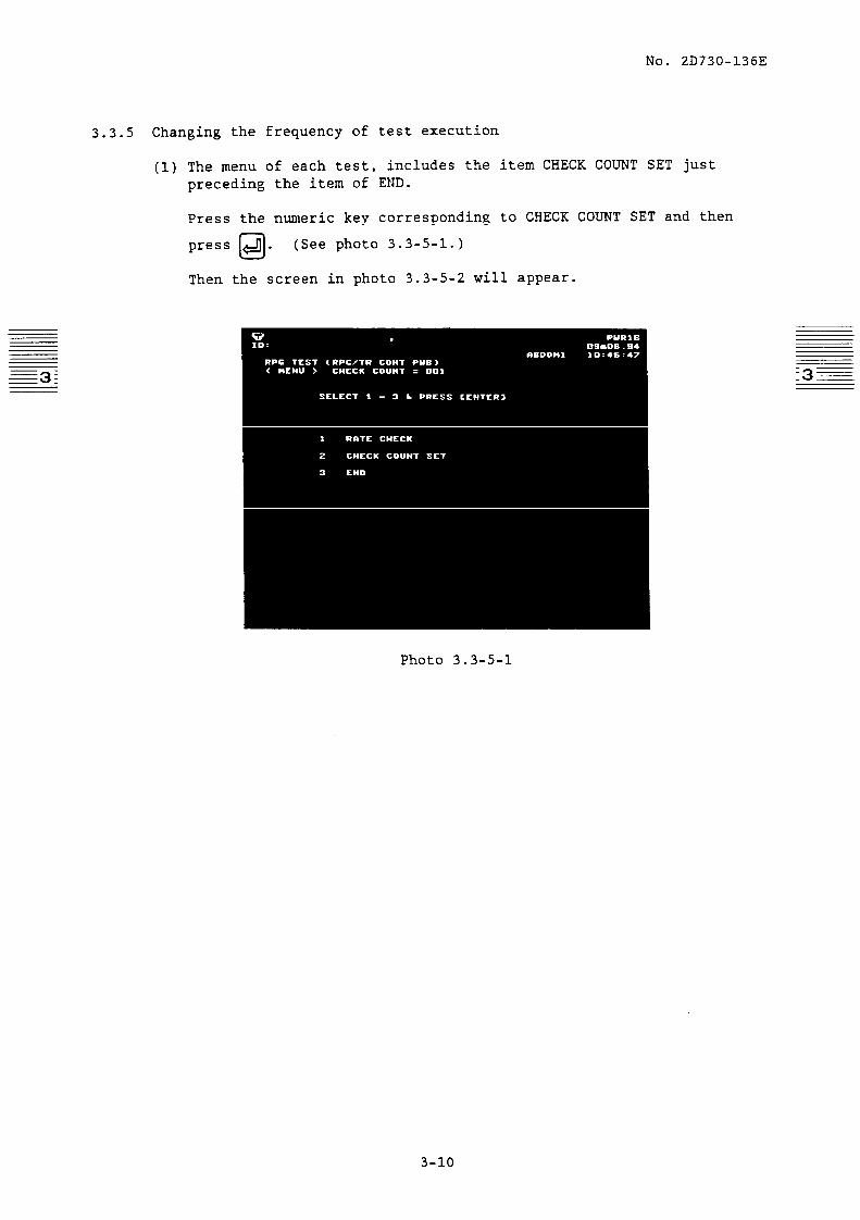
3.3.5 Changing the frequency of test execution
(1) The menu of each test, includes the item CHECK COUNT SET just
preceding the item of END.
Press the numeric key corresponding to CHECK COUNT SET and then
press +Jj. 0 (See photo 3.3-5-l.)
Then the screen in photo 3.3-5-2 will appear.
Photo 3.3-5-l
3-10

No. 2D730-136E
(2) Press the numeric key corresponding to the desired text execution
frequency and then press 4 . U When [0] and 141 are pressed, the frequency will be an unlimited
number of times.
Photo 3.3-5-2
3-11
No. 29733-136Z
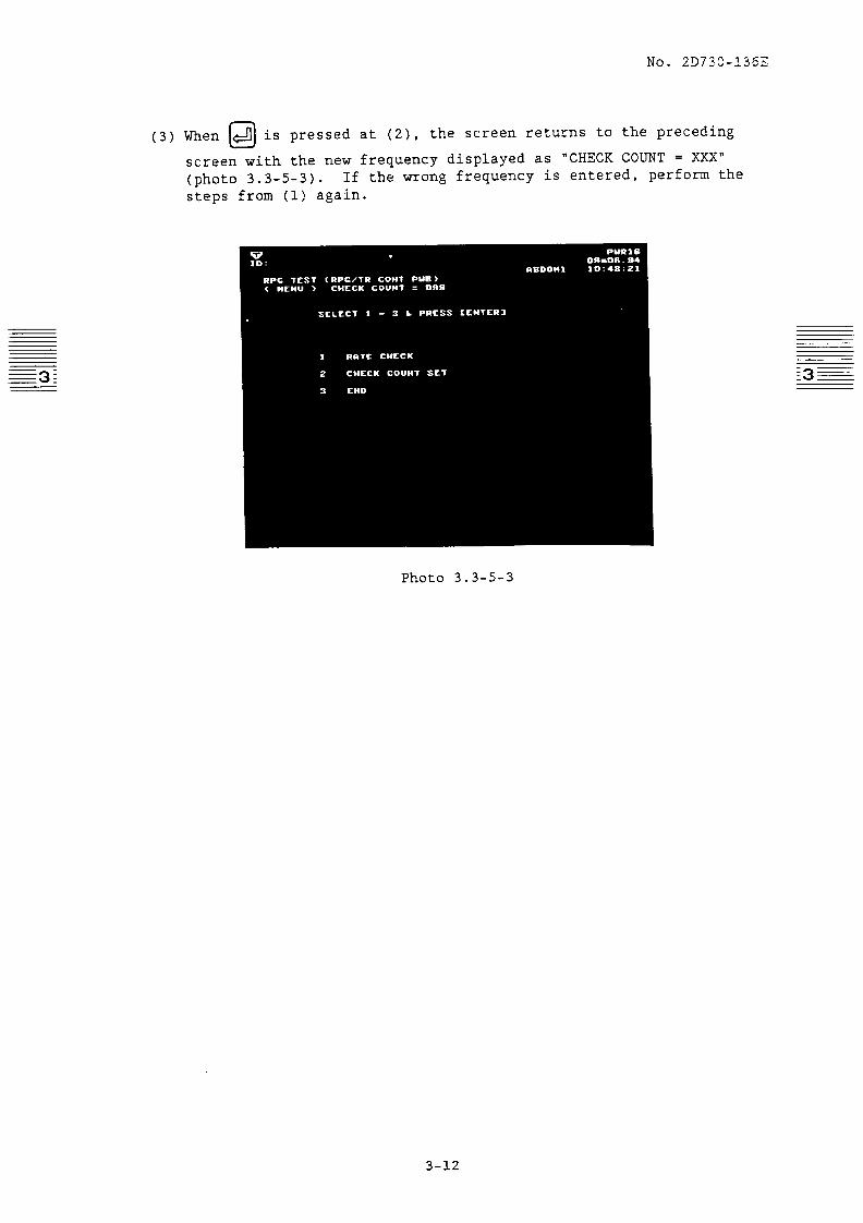
(3) When a is pressed at (2), the screen returns to the preceding
screen with the new frequency displayed as "CHECK COUNT = XXX" (photo 3.3-5-3). If the wrong frequency is entered, perform the
steps from (1) again.
Photo 3.3-5-3
3-12

No. 20730-136E
3.4 Error Code Table
The error codes for visual check are described below.
Error PWB error code has occurred
CPU 00 CPU
Detail of the error
Graphic memory abnormal
Reference
No. 3 of 4.1.3
CPU 01 CPU I Centronics abnormal I No. 6 of 4.1.3
PNL 00 PANEL
I CPU
4.2.3
DSC 01 PC DSC
DSC02 RPG/TR CONT B b W DSC
Sampling address abnormal
Raster address abnormal
No. 2 of 4.4.3
No. 3 of 4.4.3 .
(-- DSC 03 B & W DSC FM-OUT GA abnormal or abnormal
/ between FM-OUT GA and GAMMARAM 1 No* 4 Of 4*4*3
DSC 04 ADC/LB/CAL CFM DSC RGB CONVERTER
RIP abnormal, etc. No. 6 of 4.4.3
DSC 05 Ditto WIP abnormal, etc. No. 7 of 4.4.3
DSC 06 CFM DSC and the FM-IN SC abnormal, etc. No. 8 of 4.4.3
subsequent PWBs
DSC 07 ADC/LB/CAL CFM DSC RGB CONVERTER
FM-OUT GA abnormal, etc. No. 9 of 4.4.3
T/R 00 Reception system abnormal 4.5
I Reception system abnormal I 4.5
T/R 02 ) I Transmission system abnormal I 4.5
T/R 03 I Delay-line system abnormal I 4.5
FFT 01 PHASE DETECTOR FFT UNIT
FFT 02 FFT/CONT/AUDIO
Analog system abnormal (PHASE DETECTOR FFT I/O)
Digital system abnormal FFT/CONT/AUDIO
4.6.2
4.6.2
FFT 03 FFT AUDIO & L/M FFT CONT
Digital system abnormal (FFT) 4.6.2
FFT 04 FFT AUDIO & L/M FFT CONT
Digital system abnormal (FFT) 4.6.2
3-13

No. 2D730-136E
Error code
CFMOl to cFMo3
cFMo4 to CFMOS
CFM06
E3; CFMll to cFM13
cFM14 to cFM15
CFM16
PWB error has occurred
CAL section on the ADC/LB/CAL PWB
(BDF)
CAL section on the ADC/LB/CAL PWB
(MDF)
CAL section on the ADC/LB/CAL PWB (BDF/MDF)
ADC/LB/PWB and FIL/CORR PWB (BDF)
ADC/LB/CAL PWB and FIL/CORR PWB (MDF)
ADC/LB/CAL PWB and FIL/CORR PWB (BDF/MDF)
Detail of the error
Abnormal ROM table and control system in the BDF channel system.
Abnormal ROM table and control system in the MDF channel system.
Abnormal ROM table and control system in the BDF/MDF channel system.
Abnormal control system and. memory channel in the BDF channel system
Abnormal control system and memory channel in the MDF channel system.
Abnormal control system and memory channel in the BDF/MDF channel system.
Reference
No. 5 to 7 of 4.7.3
No. 8 to 9 of 4.7.3
No. 10 of 4.7.3
No. 11 to 13 of 4.7.3
No. 14 to 15 of 4.7.3
No. 16 of 4.7.3
3-14

No. 2D730-136E
4. FLOWCHARTS FOR IDENTIFYING MALFUNCTIONS
4.1 Identifying Faults in the CPU Unit
4.1.1 Preparatory work
The following preparatory work is required before carrying out the tests for the CPU which are listed below:
(1) When the RS-232C interface is checked
(a) The power to the ultrasonic diagnostic equipment is switched OFF.
(b) Connect the loopback connector to the PS-232C connector on the bottom of the main panel of the diagnostic ultrasound equipment.
For the loopback connector, use the connector to which the
following pins have been connected in the shell of the DSUB-25s connector.
I) SD (pin 2) - RD (pin 3)
(c) The power to the ultrasonic diagnostic equipment is switched ON, and the CPU test is selected.
4.1.2 Flowchart for identifying malfunctions
The flow of processing of the CPU test system is shown as a flowchart. Figure 4.1-1 shows the processing flow of the entire CPU test system.
Since actual processing will proceed according to this flowchart when the test system is operated, it is recommended that the fault be
diagnosed while confirming the processing currently being performed with respect to the entire test system by referring to this flowchart.
4-l

No. 2D730-136E
f
4-2
No. 2D730-136E
4.1.3 Decision criteria
This section shows decision criteria (normal or abnormal) for results of the tests performed according to the flowchart in section 4.1.2, depending on the messages resulting from images obtained.
Items which do not match the normal data shown here are faults as test results and faulty portions.
4-3
No. 2D730-136E
Photo 4.1-l
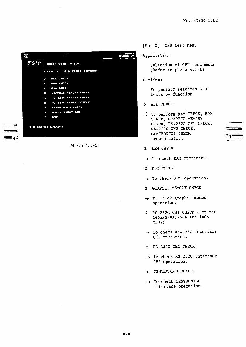
[No. 0] CPU test menu
Application:
Selection of CPU test menu (Refer to photo 4.1-l)
Outline:
To perform selected CPU tests by function
0 ALL CHECK
4
1
+
2
+
3
-+
4
+
X
+
X
+
To perform RAM'CHECR, ROM CHECK, GRAPHIC MEMORY CHECK, RS-232C CHl CHECK, RS-232C CH2 CHECK, CENTRONICS CHECK sequentially.
RAM CHECK
To check RAM operation.
ROM CHECK
To check ROM operation.
GRAPHIC MEMORY CHECK
To check graphic memory operation.
RS-232C CHl CHECK (For the 160A/270A/250A and 140A CPUS)
To check RS-232C interface CHl operation.
RS-232C CH2 CHECK
To check RS-232C interface CH2 operation.
CENTRONICS CHECK
To check CENTRONICS interface operation.
4-4

No. 2D730-136E
7 CHECK COUNT
+ To set the frequency of the CPU test. (This is preset
at a frequency of one normally.)
8 END
+ To complete the CPU test and return to the main menu.
Procedure:
+ To input the No. of the test which is to be performed
Example . . . . . ROM CHECK
Input 123 order.
H in that
Note:
Before performing a check, including the RS-232C CHl CHECK, RS-232C CH2 CHECK, and CENTRONICS CHECK, refer to 4.1.1 Preparatory work.
4-5

No. 2D730-136E
[No. 13 CPU RAM CHECK
Photo 4.1-Z
Application:
Operation check of RAM for the CPU program
Outline:
After data is written into RAM, data is read, then compared with the written data. If they do not match, non-matching addresses are indicated.
Procedure:
1)
2)
3)
The CPU carries out the test automatically and i4E
displays the message in 1):
**Jr CPU RAM CHECK Jr**
Results are displayed sequentially in the RAM unit.
When test results are normal:
The displayed image is as shown in photo 4.1-2.
The system advances to the next CHECK (CPU ROM CHECK)
when n +JJ is pressed.
The CPU test menu is
displayed when + is pressed.
0
4-6

No. 2D730-136E
4) When test results are abnormal:
Based on the results of comparison, abnormal addresses are displayed.
Bits set to "1" indicate bits with abnormal RAM.
If [F] is pressed, advances to the next address.
If [C] is pressed, completes the present MM check, and performs the next RAM check.
Operation upon completion of all addresses is the
;4=
same as in 3) above.
RAM showing abnormal addresses in the above tests are faulty. Replace the CPU PWB.
4-7

No. 2D730-136E
z:.
IIt CPU ROM CHECK tf* * CPU PUB
13Y (X08) llF7 OK 12Y (X10) FPZF OK 1DY (X18) 665E OK 12v (X30) 1645 OK 1DV (X38) 6763 OK 12T (X40) 5161 OK 1DT (X48) F674 OK 12R (X50) BDPl OK 1DR (X59) DD25 OK END
PUR16 llml7.94
RBDOMl 20:!56:55
Photo 4.1-3
[No. 21 CPU ROM CHECK
Application:
Operation check of ROM for the CPU program
Outline:
Checksum is performed by reading the contents of ROM, then comparison is made with the previous checksum results, and IC locations and checksum results (OK = normal) are indicated.
Procedure:
The CPU carries out the test :4=
automatically, and displays the message in 1):
1) *** CPU ROM CHECK ***
2) Results are displayed sequentially for each ROM unit.
3) When test results are normal:
The displayed image is as shown in photo 4.1-3.
With Isl) ON, the system
advances to the next CHECK (GRAPHIC MEMORY).
With u ON, the CPU test
menu is displayed.
4) When test results are abnormal:
The location of abnormal ROM is displayed.
Operations upon completion of all ROM CHECKS are the same as those in 3) above.
Abnormal ROM is identified from the above results. Faulty ROM should be replaced.
4-8

No. 2D730-136E
[No. 31 GRAPHIC MEMORY CHECK
Photo 4.1-4
Application:
Operation check of CPU GRAPHIC MEMORY
Outline:
"1" and "0" are written on 6 planes of GRAPHIC MEMORY.
The CRT screen will appear black and white. (With the color display, the CRT screen will appear green and blue.)
Procedure:
2)
3)
Check visually that the CRT screen displays a normal black and white pattern.
*Jr* GRAPHIC MEMORY CHECK *Jr* (Refer to photo 4.1-4)
The test starts when 4 is pressed.
0 When test results are normal:
The CRT screen becomes "white" as shown in photo 4.1-5. Then, when [F] is pressed, the CRT screen becomes "black" as shown in photo 4.1-6, permitting visual check.
If [F] is pressed, the next GRAPHIC MEMORY CHECK is performed.
Photo 4.1-5 After checking 6 planes of GRAPHIC MEMORY, the system advances to the next CHECK
when 4 is pressed. U (RS-232C CHl CHECK).
The CPU test menu is
displayed when + is pressed. 0
4-9


No. 2D730-136E
Photo 4.1-8
Photo 4.1-9
[No. 41 RS-232C (CHl) CHECK
Application:
Transmission and reception check for the CPU RS-232C interface CHl
Outline:
The contents of transmission from the equipment and reception from the return connector are compared, and-if the two do not agree, an error is indicated.
Procedure:
The CPU carries out the test automatically and displays the message in 1):
1) **Jr RS-232C (CHl) CHECK ***
2) When test results are normal:
The displayed image is as shown in photo 4.1-8.
The system advances to the
next CHECK when 4 is pressed.
0 (RS-232C CH2 CHECK).
The CPU test menu is
displayed when + is pressed.
0 3) When test results are
abnormal:
An error message is displayed as shown in photo 4.1-9.
Types and meanings of error messages are given in table 4.1-1.
Operations after display of an error message are the same as in 2) above.
4-11

No. 2D730-136E
-4i
No. Error message
FRAMING ERROR
OVERRUN ERROR
PARITY ERROR
TIME OUT ERROR
5
6
NO ANSWER BACK
COMPARE ERROR
Note:
Before performing this CHECK, refer to 4.1.1 Preparatory work.
If the return connector is not connected, a NO ANSWER BACK occurs.
Table 4.1-1 Error messages
Meaning
Format of 1 character received is not correct.
Before 1 character received is processed, the next character is received.
A parity error has occurred within 1 character received.
Transmission could not be performed within one minute upon completion of preparation.
Text could not be received.
Transmitted and received text do not agree.
4-12
No. 2D730-136E
4.1.4 Supplement
The checksum value must be registered prior to the CPU ROM check. Two
different registration methods are available.
(1) Refer to subsection 4.8.
(2) This method clears the preset data, and requires resetting of the
preset data.
(a)
(b)
w
(d)
Turn on No. 3 of the DIP SW on the CPU PWB.
Turn on the power.
When the following message is displayed, key-in Y:
INITIALIZE PRESET DATA ARE YOU SURE?
After the initial screen displaying a B mode image appears, turn off No. 3 of the DIP SW.
Note: The above procedure has been already performed before shipment from the factory.
4.2 Identifying Faults in the PANEL Unit
4.2.1 Preparatory work
No preparatory work is required.
4.2.2 Flowchart for identifying faults
START cr’ The LED on the panel blinks at intervals of approx. 1 second.
Figure 4.2-l
4-13

No. 2D730-136E”B
4.2.3 Criteria
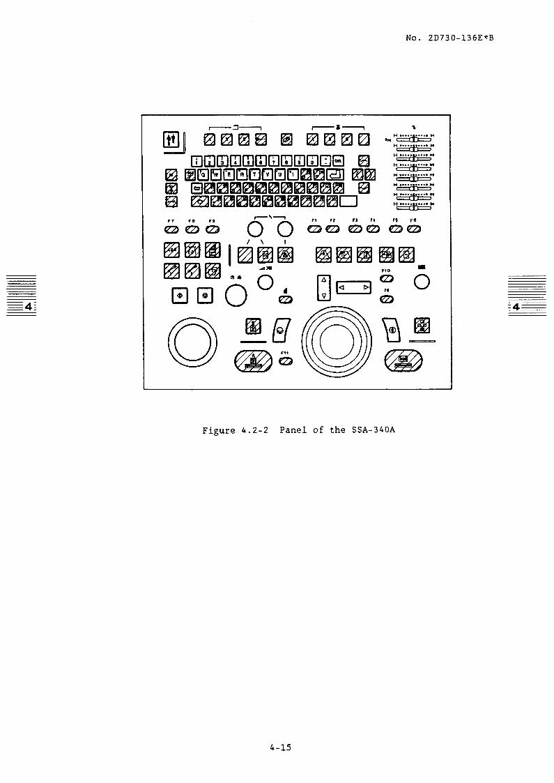
(Purpose) To identify faults in the PANEL unit.
(Outline) Turns the LEDs of the switches
indicated by in figure 4.2-2 ON/OFF at intervals
of approximately one second.
Not all LEDs on the PANEL are turned OFF/ON at intervals of about 1 s (Some LEDs may be always on, always off, or going OFF/ON at intervals other than 1 s).
I (1) Either the LEDs of switches not on . _ 1
the full keyboard are abnormal
(2) Ke LEDs of switches on the
No Both groups (1) and (2) are abnormal.
l . keyboard are abnormal. I I
It is highly probable that the PANEL is faulty.
It is highly probable that the CPU PWB or the cable between the CPU and the PANEL is faulty. . (If the panel data bus is faulty, LEDs in both groups (1) and (2) will be abnormal, regardless of the panel’s condition.)
Note : The above is based on the assumption that the D & D MOTHER PWB is normal.
4-14
No. 2D730-136E*B
a ” . . . . . . . . . . .
” . . . . . & . . . . . M
” .r... . . . . . M
“z+ ” . . . . . . . . . . w
“WM
Figure 4.2-2 Panel of the SSA-340A
4-15

No. 2D730-136E
4.2.4 Supplement
CPU
I=- a AA
Trackball, STC VR data 1 D&D MOTHER INITIAL
Data bus Address bus
1 I b .
* Cable
I 1
PAN-EL
Figure 4.2-3 Peripheral control signal path
4-16


No. 2D730-136E
4.3 Identifying Faults in RPG
4.3.1 Preparatory work
None
4.3.2 Troubleshooting flowchart
Troubleshooting procedures for RPG faults are shown in the flowchart.
<RPG CHECK>
START cr’ Checking of various enable signals, raster addresses, OF, generated in the RFG
4-18

Signal names and functions which can be checked using this test program and PWB names which utilize these signals are shown in the table below.
Signal name
(between boards)
BSAENO
MlSAENO
MZSAENO
DSAENO
FFTCMDO c-
BDFSAENO
MDFSAENO
DFINTO
DFA*O (3 bit)
TRAST*O Raster address for 0
(12 bit) transmission and reception
DRAST*O Raster address for (12 bit) indication
Function
CPU
Signal showing B mode echo o sampling rate
k Signal showing Ml mode echo o sampling rate
Signal showing M2 mode echo sampling rate
Signal showing D mode echo o sampling rate
Signal showing MDF mode echo sampling rate
0
Signal showing initial CFM operation sampling rate
ID signal showing position o of transmission focus
PWB utilizing the signal
B & W DSC CFM DSC IMAGE MEMORY FFT/CONT/AUDIO MIT CONT ECG/NON FADE
0 0 0
0 0 0 0
0
0 0 0 0
0 0
0 0
0
0 0 0
0 0 0

No. 2D730-136E
4.3.3 Decision tree
From the test results, normal (OK) or abnormal (NG) is determined for each signal as shown below.
If NG is indicated, it is highly likely that the RPG PWB is faulty, and the PWB should be replaced.
4-20
No. 2D730-136E
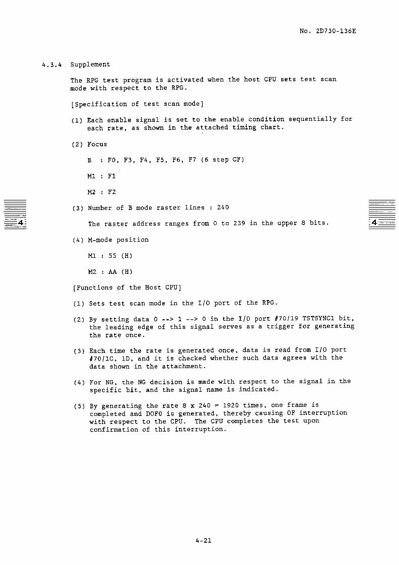
4.3.4 Supplement
The RPG test program is activated when the host CPU sets test scan mode with respect to the RPG.
[Specification of test scan mode]
(1) Each enable signal is set to the enable condition sequentially for each rate, as shown in the attached timing chart. _.
(2) Focus
B : FO, F3, F4, F5, F6, F7 (6 step CF)
Ml : Fl
M2 : F2
(3) Number of B mode raster lines : 240
The raster address ranges from 0 to 239 in the upper 8 bits.
(4) M-mode position
Ml : 55 (H)
M2 : AA (H)
[Functions of the Host CPU]
(1)
(2)
(3)
(4)
(5)
Sets test scan mode in the I/O port of the RPG.
By setting data 0 --> 1 --> 0 in the I/O port #70/19 TSTSYNCl bit, the leading edge of this signal serves as a trigger for generating the rate once.
Each time the rate is generated once, data is read from I/O port #7O/lC, lD, and it is checked whether such data agrees with the data shown in the attachment.
For NG, the NG decision is made with respect to the signal in the specific bit, and the signal name is indicated.
By generating the rate 8 x 240 = 1920 times, one frame is completed and DOFO is generated, thereby causing OF interruption
with respect to the CPU. The CPU completes the test upon confirmation of this interruption.
4-21

No. 2D730-136E
._ _
I: me- C
_L
s .
__ _-_--.
-----.
_-----.
a----_
_-----
we_
.
1T
_-a I: ._.
r
_
-r
L
-me c
aho
qe
se
sues .-_
c
,-- .
ozo
ovv
055
ahoqo S
t? aum
S
ozo
010
ovv
05s
CM
OqlZ
66
EU
lIt?S
OT
0
___
C
__
08L
0 9
9
oz5
OT
9
80C
‘Ioz
ZOT
(H) T 0
0
3IIOL #
0 00
0 vv
0 25
(H)
0 00
1 aI/of
i
1 eqep alod
30 sanTaA
anzLl

No. 2D730-136E
4.4 Identifying Faults in the DSC Unit
4.4.1 Preparations
No preparations are required to test the DSC.
4.4.2 Troubleshooting flowchart
Figure 4-11 shows a flowchart for DSC unit test system processing. This flowchart shows the actual processing flow.
When operating the test system, perform troubleshooting by checking the current processing on the flowchart.
4-23

<DSC TEST>
I I I 0: ALL
CHECK
B/W FMAO-I, FMBO-1
I B/W DSC test pattern Ckk I
I Color FMAO-2, FMBO- R/W check
I cola crJcul8ta tcu paean check I
I
I Cola LIP test Pattun ChCCk I
1: B/WFM 2: BIWTEST 3: B/WTEST CPuR/w PATTERN PA-lTERN
(SYNC) (ASYNC)
B/W
c P&k
I
B/W FMAl R/W check
I B/W FMBO R/W check
I B/W FMBl R/W check
I RETURN
4: R/wLrP 5: COLOR 6: CALTEST TEST FJMRAM PATIERN PAlTERN R/W (RI
7: CALTEST 8: COLOR 9: COLOR lo: END PATI-ERN PRIP TEST LIP TEST
(THETA) PATTERN PATTERN
I Cola FMBO R/W check I
Figure 4-l 1

No. 2D730-136E
4.4.3 Criteria
This section describes the criteria for normality or abnormality, based on the messages displayed on the screen, for the results of tests performed according to the flowchart.
If any test item does not meet the requirements, it is rejected.
4-25

No. 2D730-136E
NO
Faulty PWB: CPU B & W DSC 4
NG
Frame memory error. Faulty PWB: B&WDSC
(CPV)
I
OK
Raster address or transmission stage count error. Faulty PWB: B&WDSC RPG/IR CONT
I No error in LIP and subsequent units
Figure 4-12
4-26

No. 2D730-136E
NO
, Faulty PWB: CPU B_& W DSC
NG END
Frame memory ermr. Faulty PWB: CFMDSC . (CPv)
I
OK
NG
Sampling address error. Faulty PWB: CFM DSC
OK
The DSC unit is normal. No signal is sent from the CFM unit.
Raster address error Faulty PWB: CFM DSC RPGIrR CONT
b A
4-27
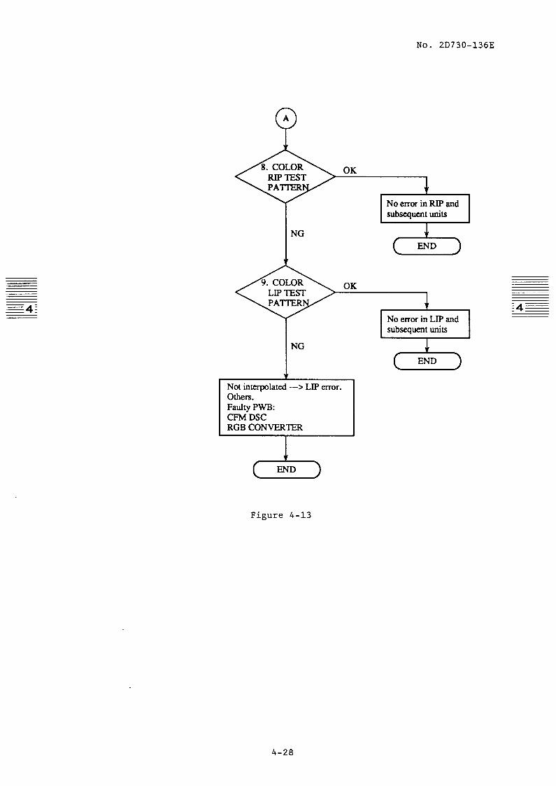
No. 2D730-136E
No error in RIP and
OK
No error in LIP and subsequent units I
A END
Figure 4-13
4-28

No. 2D730-136E
Note: If the gradation is abnormal, proceed to the test of the next item. If the gradation becomes normal at item "n", it shows that the path of the signal at item "n-l" not included in the signal of item "n" is abnormal.
Abnormal Normal Item "n" Item "n-l"
Faulty PWB
2
{ I 4 B & W DSC 3
4 ___ B & W DSC
8 CFM unit, CFM DSC
8 9 CFM DSC
yr---- 1 CFM DSC, RGB CONVERTER
4-29

No. 2D730-136E
Image mode at the time of DSC test
No. 2 B/W TEST PATTERN (SYNC)
I
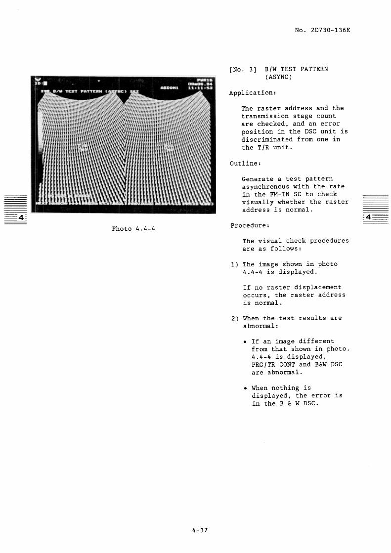
No. 3 B/W TEST PATTERN (ASYNC)
No. 4 B/W LIP TEST PATTERN
No. 6 CAL TEST PATTERN (R)
No. 7 CAL TEST PATTERN (THETA)
No. 8 COLOR RIP TEST PATTERN
No. 9
COLOR LIP TEST PATTERN
TV display
FMA I
FMB
TV1 TV2
TV? TV2
FMA FMB
I
TV? TV2
FMA FMB
,
TV? TV2
Display mode
!4tB
B-Dual
B-Dual
MtB
B-Dual
B-Dual
B-Dual
4-30
No. 2D730-136E
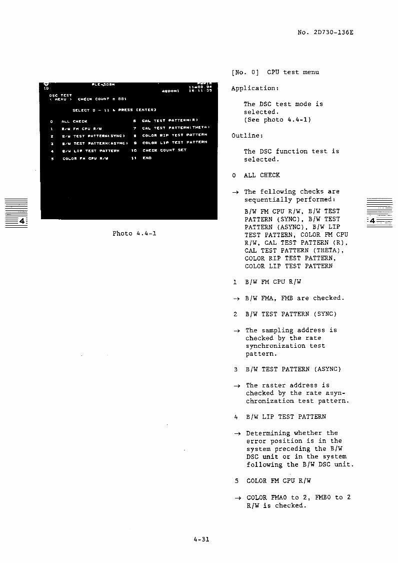
[No. 0] CPU test menu
Application:
The DSC test mode is selected. (See photo 4.4-l)
Outline:
The DSC function test is selected.
0 ALL CHECK
The following checks are sequentially performed:
B/W FM CPU R/W, B/W TEST PATTERN (SYNC), B/W TEST PATTERN (ASYNC), B/W LIP TEST PATTERN, COLOR FM CPU R/W, CAL TEST PATTERN (R), CAL TEST PATTERN (THETA), COLOR RIP TEST PATTERN, COLOR LIP TEST PATTERN
Photo 4.4-l
1 B/W FM CPU R/W
+ B/W FMA, FMB are checked.
2 B/W TEST PATTERN (SYNC)
-+ The sampling address is checked by the rate synchronization test pattern.
3 B/W TEST PATTERN (ASYNC)
+ The raster address is checked by the rate asyn- chronization test pattern.
4 B/W LIP TEST PATTERN
+ Determining whether the error position is in the system preceding the B/W DSC unit or in the system following the B/W DSC unit.
5 COLOR FM CPU R/W
+ COLOR FMAO to 2, FMBO to 2 R/W is checked.
4-31
No. 2D730-136E
6 CAL TEST PATTERN (R)
+
7
+
0
-+
9
+
11
The sampling address and r-direction thresholds are checked.
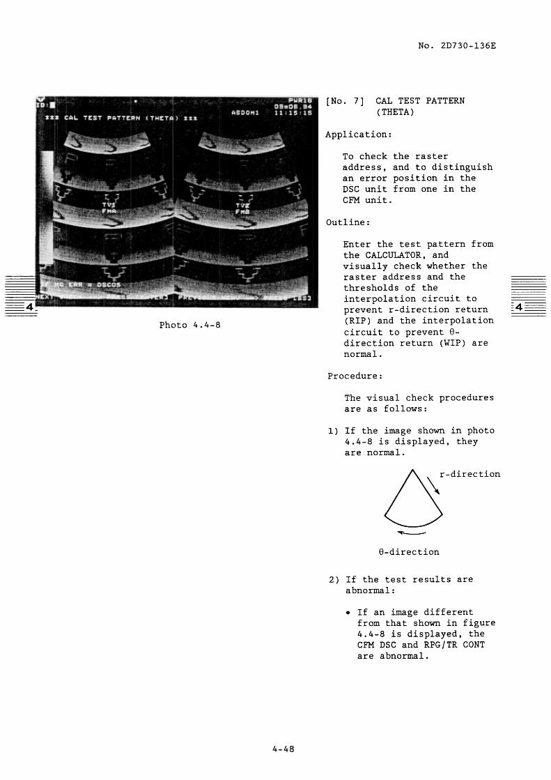
CAL TEST PATTERN (THETA)
The raster address and
r-direction and e-direction thresholds are checked.
COLOR RIP TEST PATTERN
The RIP test pattern is checked.
COLOR LIP TEST PATTERN
Determining whether the error position is in the system preceding the color DSC unit or in the system following the color DSC unit.
-LA END
+ The DSC tests are completed, and the screen returns to the main menu.
Procedure:
Enter the test number.
Example . . .
B/W TEST PATTERN (SYNC)
Input [2] @ in that order.
Caution:
Characters should be displayed on the screen. If no characters are displayed, either the CPU, B&W DSC, or CPM DSC PWB is abnormal.
4-32

No. 20730-1363
[No. l] B/W FM CPU R/W
Application:
FM memory IC operation is checked.
Outline:
Data is written into RAM, then read. If the read data does not match the written data, the address is displayed.
Procedure:
Photo 4.4-2 1)
2)
3)
4)
The CPU carries out the test automatically, and displays the message in 1): i4E
**** B/W FM RAM CHECK ***Jr
The result is displayed sequentially for each RAM.
When F'MAO is completed, FMAl and FMBO are checked in that order.
When the test results are normal, the image shown in photo 4.4-2 is displayed.
When 4 is pressed, it 0 proceeds to the next check (B/W TEST PATTERN (SYNC)).
When * is pressed, the 0 DSC test menu is displayed.
The error address and the comparison result are displayed. A bit which is set to 1 is an error bit in the RAM.
4-33

No. 2D730-136E
If the [F] key is pressed, the next address is tested.
When [C] is pressed, this check is terminated.
The operations when all addresses have been tested are the same as the operations described in 4).
4-34


No. 2D730-136E
+- 4 a
X
3
ml
4-36

No. 2D730-136E
3) When +!I is pressed, the 0 operation proceeds to the next check (B/W LIP TEST PATTERN).
When + is pressed, the U DSC test menu is displayed.
Note:
When both check results, B/W TEST PATTERN (ASYNC) and B/W TEST PATTERN
(SYNC). are normal, the DSC unit is normal. No signal is sent from the Receiver.
4-38

No. 2D730-136E
u4 0
4-39

No. 2D730-136E
Note:
If the check result is normal and no pattern is displayed when B/W TEST PATTERN (SYNC) or B/W TEST PATTERN (ASYNC) is checked, the error is in the system from the FM-IN SC to the FM- OUT.
4-41

BaW DSC
Flow chart of B/W LIP TEST PATTERN signal
I t
I Character
7
CONTROL
BLOCK 0 RPG
,
. * 66000
BLOCK o HOST
CPU
ENC/
DEL

No. 2D730-136E
Photo 4.4-6
[No. 51 COLOR FM CPU R/W
Application:
EM memory IC operation is checked.
Outline:
Data is written into RAM, then read. If the read data does not match the written data, the address at which the discrepancy has occurred is displayed.
Procedure:
1)
2)
3)
4)
5)
The CPU carries out the test automatically, and displays the message in 1):
**** CF'M FM RAM CHECK ****
The result is displayed sequentially for each RAM.
When FMAO is completed, F'MAl and F'MA3 are checked in that order.
When the test result is normal, the image shown in photo 4.4-6 is displayed.
When 4 is pressed, the U operation proceeds to the next check (CAL TEST PATTERN (R)).
When m is pressed, the
DSC test menu is displayed.
If COLOR FM CPU R/W is selected, the DSC test menu
is displayed when the &/ key is pressed.
0 The error address and the comparison result are displayed. A bit which is set to 1 is an error bit in the MM.
4-43

No. 2D730-136E
l If the [F] key is pressed, the next address is tested.
When [C] is pressed, this check is terminated.
The operations when all the addresses have been tested are the same as the operations in 4).
4-44


No. 2D730-136E
l If the pattern is otherwise abnormal, the error is in the CALCULATOR PWB or CPM DSC PWB.
l If no pattern is displayed, the error is in the CALCULATOR PWB, CPM DSC PWB, or RGB CONV PWB.
3) When m is pressed, the
system proceeds to the next check (CAL TEST PATTERN (THETA)).
When + is pressed, the U DSC test menu is displayed.
Note:
If both check results, CAL TEST PATTERN (R) and CAL TEST PATTERN (THETA), are normal, the DSC unit is normal. No signal is sent from the CPM unit.
4-46

No. 2D730-136E
4-47

No. 2D730-136E
l If the pattern is otherwise abnormal the error is in the CALCULATOR PWB or CPM DSC PWB.
0 If no pattern is displayed, the error is in the CALCULATOR PWB, CF'M DSC PWB or RGB CONV.
3) When +lJ is pressed, the 0 proceeds to the next check
- (COLOR RIP TEST PATTERN).
When + is pressed, the U DSC test menu is displayed.
Note:
If both check results, CAL TEST PATTERN (THETA) and CAL TEST PATTERN (R) are normal, the DSC unit is normal. No signal is sent from the CPM unit.
4-49

I I
9
x 3 5 L
I . .
1
’ a
% E
l E
L
1 z 8s~ L
I
%
( 4
No. 2D730-136E
d Y
3 3 %
4-50


No. 2D730-136E
I-
: v f 4-52

No. 2D730-136E
3)
4)
When the test results are abnormal:
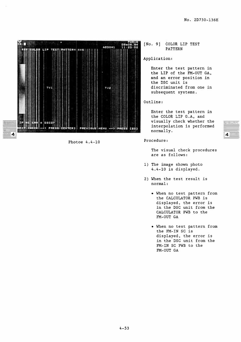
0 When interpolation is not performed normally, the error is in the FM-OUT GA.
0 When no pattern is displayed or the color tone is incorrect, the error is in the CPM DSC PWB or RGB CONVERTER PWB subsequent to the FM-OUT GA. .
If ALL CHECK or COLOR LIP TEST PATTERN is selected, the DSC test menu is
displayed when the + key 0 g4E
is pressed.
4-54

No. 2D730-136E
P-l
k’
l-l
No. 2D730-136E
4.5 Identifying Faults in the T/R Unit
4.5.1 Preparations
Ultrasonic jelly is required in the items listed below:
(1) T/R test item No. 4 R-channel check (CONVEX)
(2) T/R test item No. 5 T-channel check (CONVEX)
4.5.2 Fault diagnosis flow chart
Figure 4.5-l shows the processing for the T/R test.
4-56

<T/R TEST>
Tut mode sclactim
0: ALL CHECK
2 DLCONT RAM CHJXK
I Command RAM R/w ChCCk I
I Rccqxion chumcl chat (=W 1
l’hcT/Rtcstis complctcd 8nd Ihc. main mu is displayed once again
I
I 1 I
Figure 4.5 1
( RETURN )
No. 2D730-136E
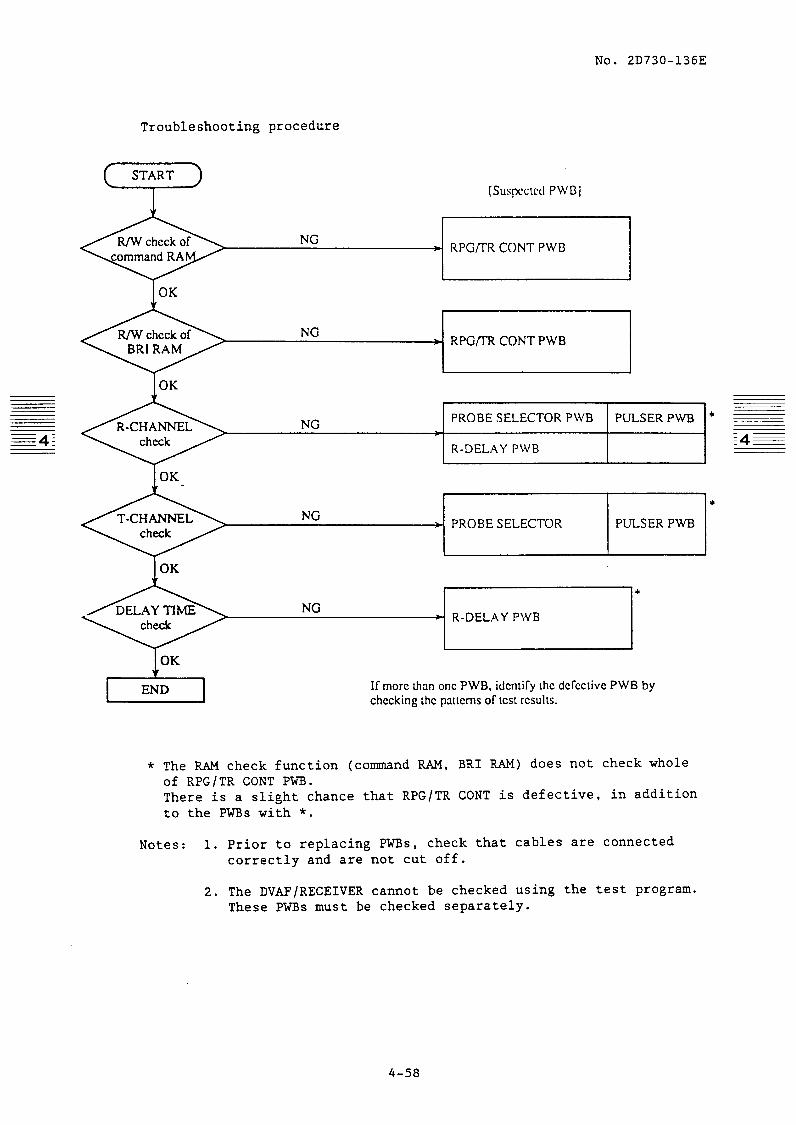
Troubleshooting procedure
[Suspcctcd PM’B 1
,
NG * RPG/l-R CONT PWB
IOK
NG * RPG/T’R CONT PWB
NG PROBE SELECTOR PWB PULSER PWB *
R-DELAY PWB *
NG w PROBE SELECTOR
*
PULSER PWB
NG
r
* R-DELAY PWB
‘*
1 END ] If more than one PWB, identify the dcfcctive PWB by checking the patterns of test results.
* The RAM check function (command RAM, BRI RAM) does not check whole
of RPGjTR CONT PWB. There is a slight chance that RPG/TR CONT is defective, in addition to the PWBs with Jr.
Notes: 1.
2.
Prior to replacing PWBs, check that cables are connected
correctly and are not cut off.
The DVAF/RECEIVER cannot be checked using the test program. These PWBs must be checked separately.
4-58

No. 2D730-136E
4.5.3 Criteria
[No. 13 T&R TEST MENU
Purpose:
T&R test menu selection
Outline:
Select the test for each block.
0 ALL CHECK
The following tests are executed sequentially.
1 T&R CONT RAM CHECK
The RAM for T/R CONTl and 2
Photo 4.5-l
delay time data is checked for read and write.
2 DELAY CONT RAM CHECK
The RAM for DELAY CONT delay time data is checked for read and write.
x R-CHANNEL CHECK (RESERVE)
4 R-CHANNEL CHECK (CONVEX)
Each channel of the convex reception system is checked.
5 T-CHANNEL CHECK (CONVEX)
Each channel of the sector transmission system is checked.
6 DELAY TIME CHECK (CONVEX)
The sector transmission - reception delay time is checked.
7 CHECK COUNT SET
4-59

No. 2D730-136E
8 END
The T&R test is completed. The [No. l] menu is displayed.
Procedure:
_ Enter the number of the test to be executed.
Example . . . . . R-CHANNEL CHECK (CONVEX)
Press the [4] and in that order.
@J keys
4-60
No. 2D730-136E
Photo 4.5-2
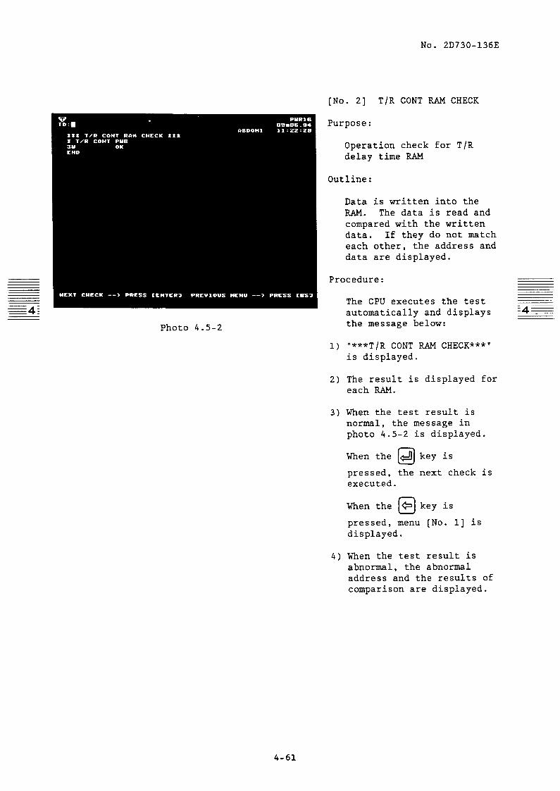
[No. 21 T/R CONT RAM CHECK
Purpose:
Operation check for T/R delay time RAM
Outline:
Data is written into the MM. The data is read and compared with the written data. If they do not match each other, the address and data are displayed.
Procedure:
The CPU executes the test automatically and displays the message below:
1) "***T/R CONT RAM CHECK***" is displayed.
2) The result is displayed for each RAM.
3) When the test result is normal, the message in photo 4.5-2 is displayed.
When the 4 key is 0 pressed, the next check is executed.
When the + key is 0 pressed, menu [No. l] is displayed.
4) When the test result is abnormal, the abnormal address and the results of comparison are displayed.
4-61
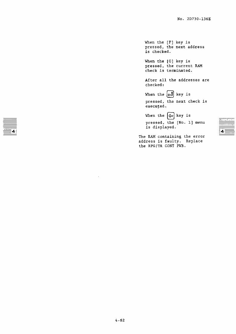
No. 20730-1363
When the [F] key is pressed, the next address is checked.
When the [C] key is pressed, the current RAM check is terminated.
After all the addresses are checked:
When the 4 key is 0 pressed, the next check is executed.
When the + key is 0 pressed, the [No. l] menu is displayed.
The RAM containing the error address is faulty. Replace
the RPG/TR CONT PWB.
4-62

No. 2D730-136E
Photo 4.5-3
[No. 31 DELAY CONT MM CHECK
Purpose:
BRI RAM operation check
Outline:
Data is written into the MM, then the data is read and compared with the written data. If they do not match each other, the address and data are displayed.
Procedure:
The CPU automatically executes the test and displays the message below:
1) "***DL CONT RAM CHECK***" is displayed.
2) The result is displayed for each RAM.
3) When the test result is normal:
a) The message in photo 4.5-3 is displayed
When the 4 key is 0 pressed, the next check is executed.
When the C=, key is U pressed, menu [No. l] is displayed.
4-63

No. 2D730-136E
4) When the test result is abnormal, the abnormal address and the result of comparison are displayed.
When the [F] key is pressed, the next address is checked.
When the [C] key is pressed, the current RAM check is terminated.
After all the addresses are checked:
When the 4 key is 0 pressed, the next check is executed. ;4---
When the + key is n pressed, the menu [No. l] is displayed.
The RAM containing the error address is faulty. Replace the RPG/TR CONT PWB.
4-64


No. 2D730-136E
When the + key is u
pressed, menu [No. l] is displayed.
When the [SPACE] key is pressed, the first half and the second half of the channels are switched. (See the figure below.)
If the values of the STC controls are set too high, the brightness of the line of a faulty channel increases, making it difficult to detect faulty channels.
CH64 cH5 t I m129 @WI
Examples:
Photo 4.5-4 shows an example of a normal result for channels 5 to 64. Photo 4.5-S shows an example of a normal result for channels 65 to 124.
For abnormal results, the defective ch is black.
4-66


No. 2D730-136E
Example
Photo 4.5.6 shows an example of normal 5 to 64 ch and photo 4.5.7 shows an example of normal 64 to 124 ch.
The marker on the raster is displayed every 10 channels.
If the channel for the transmission system is defective, the raster corresponding to the channel is black.
The gain dial has no effect, so adjust the STC ;4=
to clarify the black area.
4-68


No. 2D730-136E
3) Press the [DEL] key to terminate the delay time check. Figure 4.5.19 is displayed.
When the 4 key is 0 pressed, the next menu is displayed.
When the e key is 0 pressed, the menu No. 1 is displayed.
4) Adjust the STC controls so that a narrowest echo pattern is generated.
Photo 4.5-10
4-70
No. 2D730-136E
4.5.4 Supplement
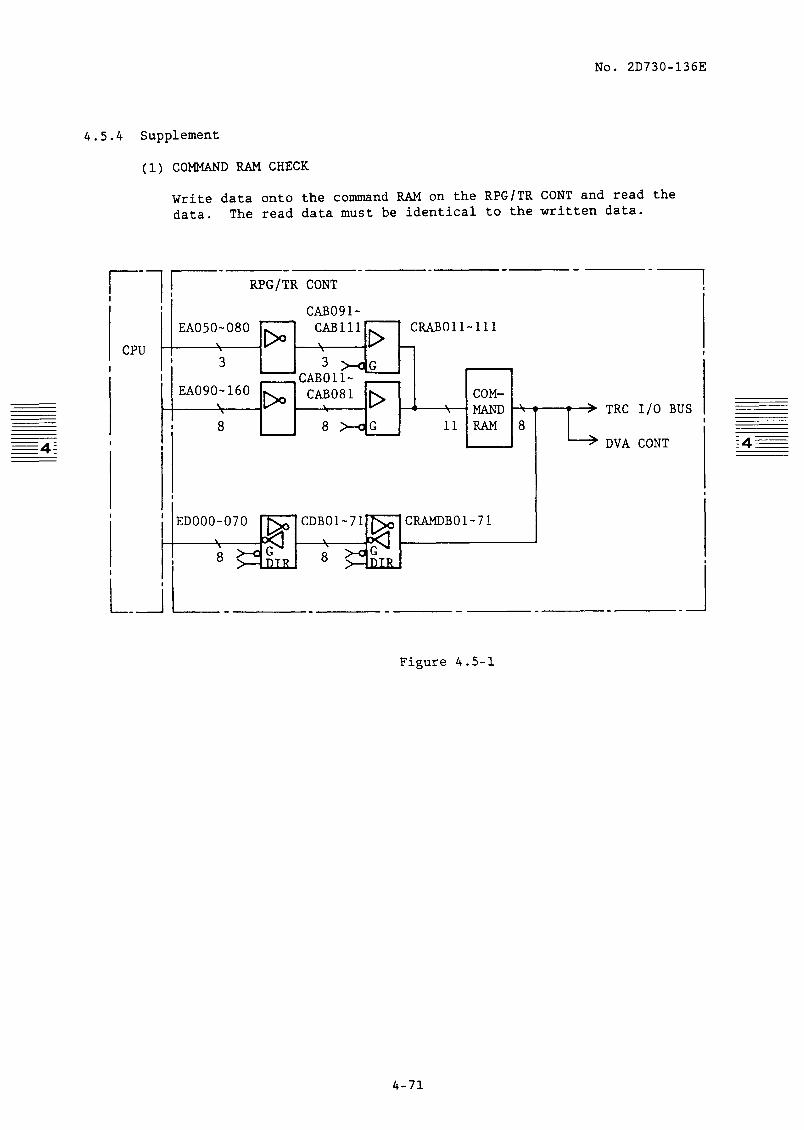
(1) COMMAND RAM CHECK
Write data onto the command RAM on the RPG/TR CONT and read the data. The read data must be identical to the written data.
I RPG/TR CONT I
I cABo91-
CPU
EAOSO-080 T ’ cAB111' \ . ,Do. ',
CRAB01 .D _
I 3 3-G. I CABOll- ,
EA090-160 _I>o.
CAB081 \ \ .D .+ \ \ . \
i a 8 FOG 11 \
+; l TRC I/O BUS 8 I
+ DVA CONT
Figure 4.5-l
4-71
No. 2D730-136E
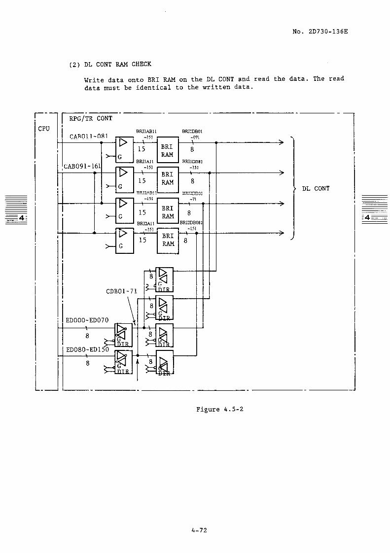
(2) DL CONT RAM CHECK
Write data onto BRI RAM on the DL CONT and read the data. The read data must be identical to the written data.
I I RPG/TR CONT I
BRIM31 1 BRIlDBOl
c~~Oll=081 ' -151 . -071 \ ’ \ 1
BRI \
I 15 8 >-G
BRIlAll 1 BRIlDBIl
,cmO91- 161 -151 h -151 \
’ 7 BRI - ‘, 15 w 8
i I *G
I I - BRK?.ABll- BRI2DBOl
I i +,;
-151 ’ ’ -71 L 1 BRI
I >-G 15 RAM 8
BRIZAll * - BRI2DBOS
. -151 -151 c A \ 1 I a I
15 BRI ' ' 7
t-G RAM 8
, 1
CDBOl-71
' EDOOO-ED070
-’
>
DL CONT
I
Figure 4.5-2
4-72

No. 2D730-136E
(3) T/R R channel check (convex)
For the R channel check (convex), a reception check is performed
during convex operation. It is possible to identify possible
defective Pubs if the R channel check and reception check interpolate each other. This check is based on transmission from
multiple elements and reception by a single element. The figure
below outlines this operation. Probe channels 1 to 4 and 125 to
128 cannot be checked due to limitations.
124 123 122 97 96 82 818079 78 77 51504948474645 10 9 8 7 6 5 Probe channels
II 1 w 1 IN 1 I 1 I I InI I I I 1 I I IN 1 I 1 I 11
Transmission
-------- Reception
124 123 122-- 9796 ~~~~~~~~-~~~~~-~t~-~~~~49 48 47~---_--------- 8 7 6 5 Raster
Note: The number of transmission chennels changes from 9 to 47 depending on the raster.
Figure 4.5-3
If one of the reception channels is defective, the corresponding raster is cut off. Display is as follows:
64 5ch c -c
------I
Figure 4.5-4
4-73
124 65 l -
__---_-__
f

No. 2D730-136E
(4) T/R T channel check (convex)
For the T channel check (convex), a transmission check is performed during convex operation. In combination with the R channel check (convex), follow the flowchart of figure 4.5.2-3. This check is based on transmission from a single element and reception by multiple elements. The figure below outlines this operation. Probe channels 1 to 4 and 125 to 128 cannot be checked due to limitations.
124123 122 97 96 828180 79 78 77 5150494847 46 45 10 9 8 7 6 5 Probe channels
Transmission
-------- Reception
124 123 122-97 96 ___________-______-_------- 49 48 47 ---_--------e-8 7 6 5 Raster
Note: The number of transmission chennels changes from 9 to 47 depending on the raster.
Figure 4.5-5
If one of the reception channels is defective, the corresponding raster is cut off. Display is as follows:
64 5ck
I
________-I
*
124 65 .e
Figure 4.5-6
4-74

No. 20730-136E
(5) T/R DELAY TIME CHECK (CONVEX)
In this check, only one channel is turned ON for transmission and reception, and the initial echo pattern is displayed. This
pattern is a delay track for the specified channel when scanning is performed for lines 0 to 239.
Check whether the initial echo pattern matches the graphic pattern. If they do not match each other, there is a fault in the system.
Graphic pattern
Initial echo image
(Example of convex)
Figure 4.5-7
4-75

No. 2D730-136E
>,
I 91
-I 31 - ;r PH.D OSC CHECK
t
A test signal is input to An error position is the PHASE DETECTOR distinguished from one in
I [21 the prestage (T/R unit). - c FORWARD FLOW CHECK
1
A forward flow test signal An error position is
is input to the FFT distinguished from one in
(digital section). the prestage (FFT analog
I [31 processing unit). - c REVERSE FLOW CHECK
v
A reverse flow test signal An error position is
is input to the FFT distinguished from one in
(digital section). the prestage (FFT analog
[41 'processing unit). c BLANK CHECK .
4.6 Identifying Faults in the FFT Unit
4.6.1 Preparatory work
Set the audio VR (L,R) to MIN.
4.6.2 Flowchart for identifying faults
(1) Operating procedure
Perform visual comparison check between the expected value pattern displayed on the monitor screen and the Doppler image resulting from the FFT of test signals.
<FFT TEST>
A no flow test signal is
input to the FFT (digital section).
to the next
I An error position is distinguished from one in the prestage (FFT analog processing unit).
Figure 4.6-l
4-76

No. 2D730-136E
(2) Troubleshooting expected failures of PWBs
v
- RECE I VER m , +
T/R -
SPEAKER{ L,R)
LEVEL METER
HOST CPU
RPG
Figure 4.6-Z
4-77

No. 2D730-136E
START
v v 7 PH.D OSC CHECK
6 ,
N
1 FORWARD FLOW CHECK 1
*
REVERSE FLOW CHECK
I
+A--.. I BLANK CHECK I
Failure of the PHASE DETECTOR, FFI’-I/o or FFI’/CONT/AUDIO FFI’/CONT/AUDIO
Failure of the prestage (T/R unit)
Figure 4.6-3
4-78


No. 2D730-136E
4.6.4 Supplement
When starting this test system, the normal PANEL SW does not operate,
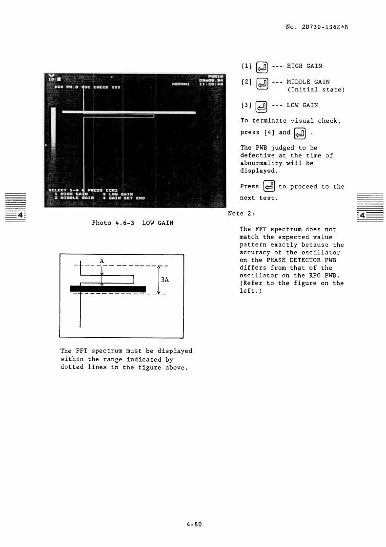
and quantitative evaluation is performed with the conditions limited to the three GAIN levels.
The changes of the FFT spectrum display can be checked by operating the PANEL SW as required as described below.
(1) PH.D OSC signal check (with the probe of 3.75MHZ and REFERENCE = M)
Turn off the test. Place it in the PATCH input mode. Write the following data.
R204000 @ W 1 @
R224000 4 0 W 80 4 0 R224044 0 4 wg 0 dJ (To release, write W 0 U +Q .)
R204000 0 &j w” 0 4 Release the PATCH input mode.
Now, the PANEL SW can be operated so changes in the image can be checked with the SW functioning. (To release it, turn off the
power or write R224044 @ W 0 @.)
Notes: 1. This check can be applied to the COLOR (BDF, MDF) as well as the PW Doppler.
2. The setting can be changed as required with the PANEL SW. Saturation and too much narrowing prevent changing some combinations.
(2) FFT CAL signal check
Turn [ON] FFT CAL using the service function.
Now, the PANEL SW can be operated to permit checking the operation of the switch. (However, the analog unit control SW = FFT GAIN is not working.)
4-86

No. 2D730-136E
4.7 Identifying Faults in the CFM Unit
4.7.1 Preparatory work
To check the system using the test pattern, set the STC-volume to the
minimum.
4.7.2 Flowchart for identifying faults
2-l Procedure
Perform self-diagnosis and visual check of the 280 of the CFM unit by the commands of the HOST CPU (68000) by the following procedure.
Hardware (CFM unit) FIL/CORR self-diagnostic pulse
4_ LB Visual ,(LB test r 1 7 c F I L CORR d CAL ’
RAM) 4, . r-y * ------%tput
/ * ‘I I *
t IL FILTER throughJself-diagnosis , ----_---
Writing in the L____________________~ LB/CAL self-diagnostic path
LB test RAM
pat tern
280
LB/CAL self-diagnostic path __-----_-_____-__-- ---_
pat$
CAL output buffer lead
Error code
generatior simulation 1
normal code
4-87

No. 20730-136E
2-2 Faults-identifying path
(1) Self-diagnostic path
(a) LB test RAM, test
ADC/LB/CAL FIL/CORR
B m test
A I
v vv
280 MT I -CONT
\
(b) LB/CAL test
ADC/LB/CA L
The shaded part (B) is to be checked.
FIL/CORR
To DSC >
280 MT I -CONT
C
To DSC m
The shaded parts ( tzI
) are to
be checked.
4-88

No. 2D730-136E
(c LB/CORR/CAL test
ADC/LB/CA I_ F 1 UCORR
MTI-CONT 280
(d LB/FIL/CORR/CAL test
ADC/LB/CA L
MT I II-- ADC
The shaded parts be checked.
(El
FIL/CORR
To DSC
are to
MT I -CONT 280
To DSC
The shaded parts (a be checked.
are to
4-89

No. 2D730-136E
(2) Visual check path
(a) CAL test patterns 1, 2 and 3
ADC/ LB/CA L F I L/CORR
MTI C ADC - -
7 /// LB 4
-test I I
v I
l’o DSC
MTI -CONT 280
, .
The shaded parts (a) are to be checked.
(b) LB test pattern 1 and 2
ADC/LB/CA L F I L/CORR
*
MTI
ADC --)
. .
To DSC
The shaded parts (B) are to be checked.
4-90

No. 2D730-136E
4.7.3 Criteria
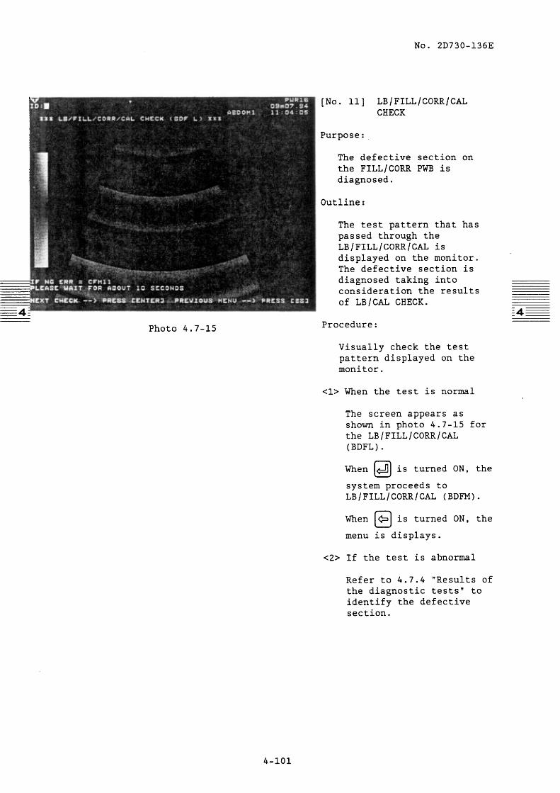
This subsection describes the criteria for determining whether the results of tests carried out according to the flowchart in 4.7.2 are abnormal based on messages displayed on the screen.
Items which do not match the normal data shown here are faults and faulty portions.
4-91

No. 2D730-136E
[No. 0] CFM test menu
Photo 4.7-l
Purpose:
Selecting the test mode for CFM (Refer to figure 4.7-l.)
Outline:
Select tests by function of WM.
0 ALL CHECK
-> Carry out test items 1 to 16 sequentially.
1 LB SELF TEST
-> Carry out self diagnosis of the LB test MM.
2 LB/CAL SELF TEST
-> Carry out self diagnosis of LB/CAL.
3 LB/CORR/CAL SELF TEST
-> Carry out self diagnoses of LB/CORR/CAL.
4 LB/FIL/CORR/CAL SELF TEST
-> Carry out self diagnoses of LB/FIL/CORR/CAL.
5 to 10 LB/CAL CHECK
-> Display the test pattern for the LB/CAL path and visually check it.
11 to 16 LB/FIL/CORR/CAL
-> Display the test pattern for the LB/FIL/CORR/CAL path and visually check it.
4-92

No. 2D730-136E
Photo 4.7-2
[No.11 LB SELF TEST
Purpose:
Self diagnosis of the LB test MM is carried out.
Outline:
R/W is performed from/to the LB test RAM to diagnose the LB test RAM by comparing written data with read data.
Procedure:
The CPU automatically performs the test and displays the results on the _4--_
monitor.
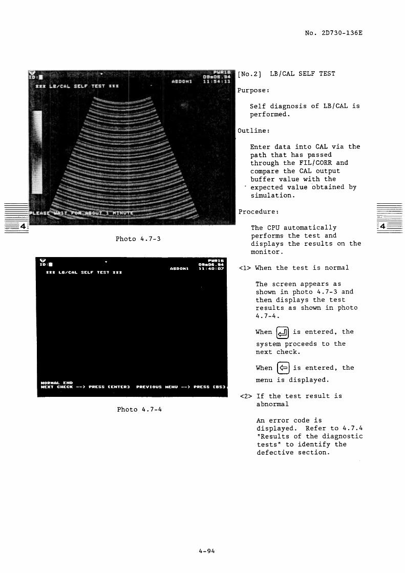
<l> When the test is normal
The screen appears as shown in photo 4.7-2 after a transit image has been displayed.
When 4 is (entered, the 0 system proceeds to the next check.
When + is entered, the 0 menu is displayed.
<2> If the test result is abnormal
An error code is displayed.
Refer to 4.7.4 "Results of the diagnostic tests" to identify the defective section.
4-93


No. 2D730-136E
4.7.4 Results of the diagnostic tests
(1) Definition of error codes of self-diagnosis
MSB 15 14 13 12 11 10 9 8 7 6 5 4 3 2 1 0 LSB r
10 0 0 0 0 0 0
Description of error Error code
Normal 0 0 0 0 0 0 0 0 00
LB test RAM abnormal 0 0 0 0 0 0 0 1 01
LB/CAL v abnormal 010 0 0 0 01 41
LB/CAL P abnormal 010 0 0'010 42
LB/CAL 0 abnormal 010 0 010 0 44
LB/FIL/CORR/CAL 10 0 010 0 0 88 v abnormal
LB/FIL/CORR/CAL 10 010 0 0 0 90 P abnormal
LB/FIL/CORR/CAL 1010 0 0 0 0 A0 CT abnormal
LB/CORR/CAL 010 010 0 0 48 v abnormal
LB/CORR/CAL 01010 0 0 0 50 P abnormal
LB/CORR/CAL 0110 0 0 0 0 60 (r abnormal
4-105

No. 2D730-136E
(2) Example
r lame of the ;elf-diagnostic
Lest applied
Faulty PWBs Error code PWB name Details of fault
,B test RAM test 01 [TI-CONT 1) 280 I/F section with LB/CAL abnormal (Location: OS, OR, OT, OQ)
12) 280 and 280 peripheral (ROM, RAM) abnormal (Location: 7T, 3S, 5T etc.)
LDC/LB/CAL ;l) Test RAM abnormal (Location: 12G, 12F and 12E)
:2) I/F section with Z80 abnormal (Location: B2P, BlN, BlP, BlM, 14F, 14E, 14C, B12D, B12A, B13A, 12D)
41 (Note 1)
ITI-CONT ,B/CAL test (1) Control unit abnormal (Location: 35, 2L, 2M, 25, 2H, lL, lJ, lH, 2C, lD, OD etc.)
DC/LB/CAL (1) Operation ROM table section (circuit diagram page 10/14) abnormal
(2) CAL output buffer section 280 I/F defective (Location: B6K, 7G, 6J, 8G, 6H, B5F, B5E)
(3) CAL output buffer RAM abnormal (Location: 6G and 6F)
(4) CAL output buffer memory read/write control section abnormal (Circuit diagram page 13114)
(5) Data number encode section (location B3P and 3N) and gradation cut control code (location BlR) abnormal
D b D MOTHER (1) MTI-CONT PWB, ADC/LB/CAL PWB mother board contact defective
42 (Note 1)
MTI-CONT (1) MTI-CONT PWB, LB/CAL PWB mother board contact defective
LB/CAL test
LB/CAL
D & D MOTHER
LB/CAL test 44 (Note 1)
MTI-CONT Same as above
LB/CAL
D & D MOTHER
4-106

No. 2D730-136E
Error code
48
(Note 2)
50 (Note 2)
60 (Note 2)
88 (Note 3)
PWB name
[TI-CONT
IL/CORR
1 & D MOTHER
4TI-CONT
'IL/CORR
1 & D MOTHER
4TI-CONT
FIL/CORR
D b D MOTHER
qTI-CONT
FIL/CORR
D b D MOTHER
Faulty PWBs
Details of fault
1) Control unit abnormal (Location: lY, lBB, lAA, OCC, 3DD, ODD, ZDD, XC, 7D, 5B, OBB etc.)
1) CORR section control PAL abnormal (Location: 4G, 45, 4L, 55, 5F, 3K,
3L)
2) Discrete logic around the above control PAL is abnormal
3) CORR Z-I memory (location 8D and 7D) and C memory (location 7A to 7C and 8C) abnormal
14) Gate array (location 7K) abnormal
15) FILTER through gate (location 2W, 3V, 3W) operation defective
11) Contact of the MT1 CONT PWB, ADC/LB/CAL PWB FIL/CORR PWB with the mother board defective
same as above
same as above
(1) Control unit defective (Location: lY, lBB, lAA, OCC, 3DD, ODD, 2DD, 2CC, 7D, 5B, OBB etc.)
(1) Control PAL abnormal (Location 4M, 4H, 4K, 4G, 45, 4L, 3K, 3L, 5H, 5L, SK, 5G, 5J, 5F, 6H)
(2) Discrete logic around the above control PAL is abnormal
(3) Z-1, Z-2 memory (location 8S, 8D, 81 and 8U) abnormal or coefficient memory (location 6s and 6R) abnormal
(4) Gate array (location 5U) abnormal
(1) Contact of the MTI-CONT PWB, ADC/LB/CAL PWB, FIL/CORR PWB with the mother board defective
game of the self-diagnostic
test applied
LB/CORR/CAL test
LB/CORR/CAL test
LB/CORR/CAL test
LB/FIL/CORR/CAL test
4-107

No. 2D730-136E
Error Faulty PWBs
code I PWB name I Details of fault
90 MTI-CONT (Note 3) -
FILjCORR Same as above
ID & D MOTHER1
“ate 3, IFiSarne as above
ID & D MOTHER1
Name of the self-diagnostic
test applied
LB/FIL/CORR/ CAL test
LB/FIL/CORR/ CAL test
(Note 1): First, complete normally the LB test RAM test. (Note 2): First, complete normally the LB test RAM test and LB/CAL test. (Note 3): First,
---_ complete normally the LB test RAM test, LB/CAL test and
LB/CORR/CAL test.
4-108

No. 2D730-136E
(3) CAL test pattern
(a) CAL test pattern
No.
1
2
3
4
5
6
Phenomenon
The character S is not displayed.
The dispersion display has no gradation.
The character P is not displayed.
The power display has no gradation.
The character V is not displayed.
The speed display has no gradation.
Faulty units
(1) CAL operation ROM table speed operation unit (Location: lG, lF, BZE, BlG, BlF, BSB, 6B, SB, B6B, BSC, lOD, B8C, B6C, 8D, B8B, 8B)
(2) CAL operation power ROM unit (Location: 6D, B6C, BllC; B12B) abnormal
(1) CAL operation ROM table speed operation unit (Location: SB, SD, BSC, BSD, lOE, BlOB, BlOC, lOB, BlOE, llE, 11D) abnormal
(1) CAL operation ROM table speed operation unit abnormal
(2) CAL operation power ROM unit abnormal
(1) CAL operation power ROM unit abnormal
(1) CAL operation ROM table speed operation unit abnormal
(2) CAL operation power ROM unit abnormal
(1) CAL operation ROM table speed operation unit abnormal
(2) CAL operation power ROM unit abnormal
televant ?WB
&B/CAL
,B/CAL
LB/ CAL
Remarks
If the phenomena nentioned at the left occur together, the cause may be one of the following:
Pipe line lock is out of order.
The CAL output buffer read/write is out of order.
The MT1 CONT control system is out of order.
;4---
No control signal has come from the PRG.
MTI-CONT ADC/LB/CAL D & D MOTHER
Note: When the number of MDF data is H, the characters SPW are not displayed.
4-109

No. 2D730-136E
No.
1
2
3
(b) LB test pattern
Normal display should be checked with the CAL test pattern beforehand.
Phenomenon
B There is no gradation of dispersion display.
D Dispersion display is not ’ performed.
There is no gradation of power display.
Power display is not performed.
l There is no gradation of speed display.
l Speed display is not performed
Faulty units
(1) LB section RAM (including initial value subtraction RAM) abnormal
(2) FILTER section abnormal
(3) CORR section abnormal
(4) MTI-CONT abnormal
Same as above
Same as above
Relevant PWB
ADC/LB/CAL
FIL/CORR
FIL/CORR
MTI-CONT
Same as above
Same as above
Remarks
Perform
I self-diagnosis test.
Same as above
Same as above
If any of the above phenomena occur, the cause may be the following:
(1) LB RAM read/write abnormal (2) Initial value subtraction abnormal (3) MTI-CONT control unit abnormal
(c) CAL Test Patterns 2 and 3 (for checking the DSC interpolation and threshold)
These test patterns are omitted as they are for checking the B-direction interpolation, r-direction interpolation, e-direction threshold and r-direction threshold value.
4-110
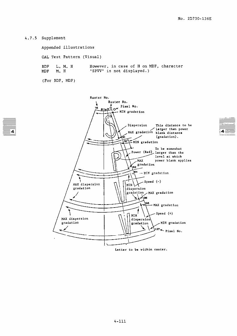
No. 2D730-136E
4.7.5 Supplement
Appended illustrations
CAL Test Pattern (Visual)
BDF L, M, H However, in case of H on MDF, character MDF M,H "SPW" is not displayed.)
(For BDF, MDF)
Raster No.
\ Raster No.
Pixel No.
HIN gradation
This distance to be /larger than power
MAX gradation blank distance
l
lat
MAX dispersion
- MIN gradat ion
C-J
gradat ion
MAX gradation
Letter to be within raster.
4-111

No. 2D730-136E
LB Test Pattern (Visual)
BDF L, K H MDF M,H
(For BDF, MDF) (Except when alternating rate.)
Note: All values of dispersion, power, etc. represent gradations.
Raster NO. Raster No.
$ rl 15 0 Pixel No.
I MAX rt i criers i nn ---r-------
i,
J I
MIN dispersion
kersion
MIN dispers
axe P persion
r
)
0 dispersion
4-112

No . 2D730-136E*C
4.8 Maintenance
Maintenance is not part of the test, but is used to support the test
Initial operation:
MAINTENANCE <MENU>
SELECT1 - 4 h PRESS [ENTER]
1 CHECK SUM
2 PWB REVISION
3 SYSTEM SETUP
4 END
Figure 4.8-l
Enter [83 cg I
, at the
stage shown in photo 3.3-1- 3. The screen shown in figure 4.8-l appears.
This maintenance menu includes the following menus: the CHECK SUM menu for registering the check sum value of the ROM directly controlled by the CPU, the PWB REVISION menu for displaying the revision of the PWB used currently for the system, and the ;4=
SYSTEM SETUP menu for DIP SW settings by the software for initialization.
When [4] is selected and
is pressed on the
screen shown in figure 4.8-1, the system returns to the screen shown in photo 3.3-1-3.
4-113

No. 2D730-136E"C
[No. 11 CHECK SUM
PLEASE WAIT FOR ABOUT 1 MINUTE.
(NOW REGISTRATION OF CHECK-SUM IS EXECUTING.)
Figure 4.8-2
On the menu shown in figure
4.8-1, enter [l] m .
and the maintenance procedure described below is performed.
Purpose/outline:
The check sum value for the ROM containing the programs of the CPU (host) is registered. The CPU ROM check described in No. 2 of subsection 4.1.3 will fail without this registration.
In addition to this registration, the check sum
:4--_
value for "self-diagnoses" is also registered simultaneously.
Procedure:
Press [l] on the
menu shown in figure 4.8-l. The screen message shown in figure 4.8-2 is displayed during execution. It takes approximately one minute to complete this step of the maintenance. After completion, the screen returns to that shown in photo 3.3-l-3 automatically.
4-114

No. 2D730-136E*C
[No. 21 PWB REVISION
PREVIOUS MENU --> PRESS [BS]
MAINTENANCE <PWB REVISION>
PWBNAME
CPU/P-IF/STC: E FE F
RPG/TR CONT : E 8 F F
ECG/NFADE : - 0 0 0
B&W DSC :- F D E
COLOR DSC : - ED E
IMAGE MEM : - F C E
FtGB/CONv : - F F F
ENC/DEC : - F F F
MT1 CONT : E F F F
FFT AUDIO : F F F F
MFEHA CONT : - FF F
Figure 4.8-3
When [Z] is entered
on the menu in figure 4.8- 1, PWB REVISION is executed as shown below.
Purpose/outline:
Displays the revision of each PWB used in the system.
Procedure:
ii-n When PI ISJ is pressed
while the menu in figure 4.8-l is displayed, PWB revisions are displayed. Figure 4.8-3 shows an example of this.
When @ D
(BS) is pressed,
the system returns to the screen in figure 4.8-l.
4-115

No . 2D730-136E*C
[No. 31 SYSTEM SETUP
When [3] IO
is pressed
on the menu shown in figure 4.8-1, the fo:Llowing settings are executed.
MAINTENANCE <SYSTEM SETUP>
SELECT 1 - 6 & PRESS [ENTER]
1 DIPSW3 : PRESET DATA
2 DIPSW5 : USER REG., UF KEY, IP
3 DIPSWC : GAMMA CORR, STC, GAIN
4 ALLON : ALL DATA(PATIENT DATA, APPLI. MEASURE)
5 ALL OFF
6 END
DIPSW3: OFF OR ON
DIPSWS: OFF OR ON
DIPSWC: OFF OR ON
Figure 4.8-4
Purpose/outline:
DIP SW3, DIP SW5, and DIP SW6 are set by the software. By these settings, EEPROM INITIALIZE processing can be started when the system is started.
Procedure:
While the menu shown in figure 4.8-4 /LS displayed,
When [l] is pressed, :4--_
DIP SW3 can be set ON/OFF.
When [Z] is pressed,
DIP SW5 can be set ON/OFF.
When [3] is pressed,
DIP SW6 can be set ON/OFF.
When [4] is pressed,
all DIP SWs can be set to ON.
When [5] is pressed,
all DIP SWs can be set to OFF.
When [6] is pressed
on the screen shown in figure 4.8-4, the screen returns to the screen shown in figure 4.8-1.
After the above dip switches are set, EEPROM initialization should be performed by turning the power OFF and then ON again or by resetting the software using the CPU RESET SW on the rear panel.
4-116

No. 2D730-136E*C
Supplement:
If one of DIP SW3, DIP SW5, and DIP SW6 on the CPU PWB is set to ON, DIP SW setting by the software is invalid.
DIP SW setting by the software is automatically set to OFF if EEPROM INITIALIZE processing is executed or interrupted.
4-117

No. 2D730-136E
5. APPENDIX
5.1 Error Codes for Self-diagnosis
Explanations up to now have concerned only test systems which are activated by service personnel.
In the SSA-340A in addition to the above test systems, other built-in test systems are provided in the equipment. These test systems monitor the ultrasound system constantly, and whenever an error occurs, a corresponding message is indicated (self-diagnosis).
The messages mentioned above are described in the service manual for the equipment. However, they are also attached here for reference. (Table 5.1-l)
5-l

Table 5.1-1 Error messages for self-diagnostic tests
Check item Purpose of test Message displayed Judge-
(nature of check) (error code) ment
RAM CHECK Confirmation of RAM operation for CPU Abnormal:
programs "ERR = 50"
[The CPU writes data into RAM and reads the same data, then performs checking by comparing the two.]
of ROM operation for CPU Abnormal: "ERR = 51"
are added and compared with data added and stored previously, and checking is performed by comparing the two.]
GDC FIFO When the power is ON and FIFO is not empty, Abnormal: CHECK the LED on the CPU PWB lights. The LED 0 on the
CPU PWB lights.
ERROR CODE Refer to table 5.1-2. Same as left
ERROR
I
Refer to table 5.1-3. Same as left
MESSAGE
CPU
CPU
CPU
CPU
CPU
Remarks
Activated once when power is turned ON.
Incorporated into the Host CPU
software as a test routine.

No. 2D730-136E
Table 5.1-2 Table of error codes
The host CPU detects errors and outputs error codes and messages.
If an error code appears on the monitor, find it in the following list:
Error code Description
5200
5201
5202
5204
5205
5206
5208
5209 The host CPU failed to access the C-RAM in the FFT/CONT/AUDIO ;5-----
5215
5218
5219
5223
5224 The host CPU received no OF interrupt (or ECG OF interrupt
5225
5226
5450
rhe local CPU of the monochrome DSC generated an interrupt but the host CPU did not receive it.
Vo FI interrupt from the PANEL I/F section on the CPU PWB in calculation of TR delay time.
The local CPU of the ECG/NONFADE board generated an interrupt but the host CPU did not receive it.
The host CPU failed to access the C-RAM in the monochrome DSC.
The host CPU failed to access the C-RAM in the color DSC.
Undefined probe ID detected by the host CPU.
The local CPU of the COLOR DSC generated an interrupt but the host CPU did not receive it.
board.
The host CPU received no OF interrupt from the RPG section on RPG/TRCONT board after sending OF RESET information to the RPG section.
The host CPU received no OF interrupt from the RPG section before sending TR OFF information to the T/R CONT section on the RPG/TRCONT PWB in freeze on mode.
The host CPU received no OF interrupt from the RPG section on the RPG/TRCONT PWB before erasing frame memory.
The host CPU received no OF interrupt from the RPG section on the RPGITRCONT PWB when it expected the interrupt.
during ECG SYNC) from the RPG section on the RPG/TRCONT PWB when the freeze switch was pressed during recording in B-LOOP image memory mode.
The host CPU received no OF interrupt from the RPG section on the RPG/TRCONT while re-recording images in image memory.
The host CPU received no OF interrupt from the RPG section on the RPG/TRCONT when the image memory is to be erased.
The host CPU failed to access the C-RAM on the ECG/NONFADE board.
5-3
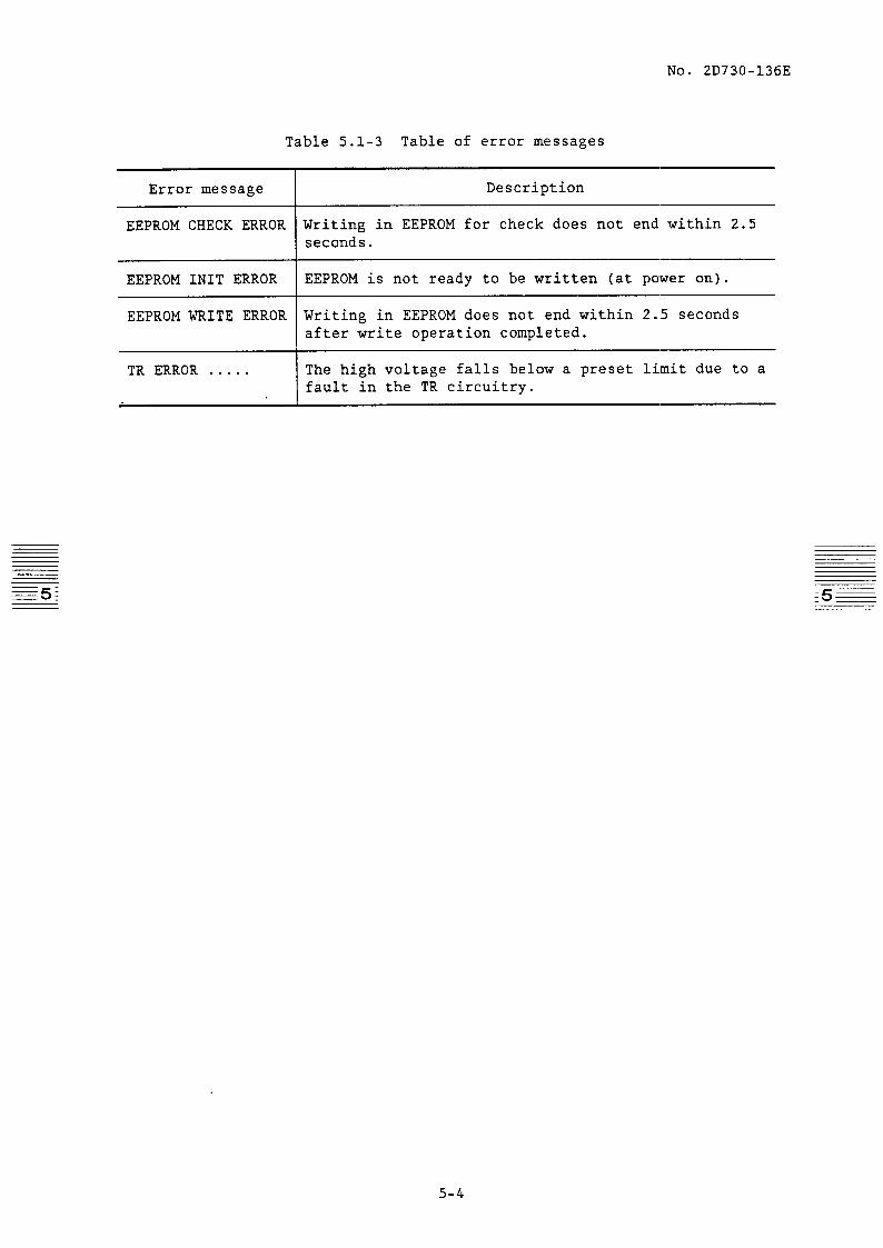
No. 2D730-136E
Table 5.1-3 Table of error messages
Error message Description
EEPROM CHECK ERROR Writing in EEPROM for check does not end within 2.5 seconds.
EEPROM INIT ERROR EEPROM is not ready to be written (at power on).
EEPROM WRITE ERROR Writing in EEPROM does not end within 2.5 seconds after write operation completed.
TR ERROR . . . . . The high voltage falls below a preset limit due to a fault in the TR circuitry.
.
5-4

No. 2D730-136E
5.2 Patch Menu Operation
5.2.1 Applicable equipment
SSA-340A
5.2.2 Starting
Important notice:
This starting procedure is for authorized personnel only (for software protection). This procedure must not be disclosed to thle user.
(1)
(2)
(3)
(4)
IsETTINGl menu, 1-1
&
On the full-keyboard =/,[:I
&
Also start with the -1 menu, by pressing Es].
The PATCH MENU is displayed.
PATCH MENU
HIT (I - 4) KEY
1. MEMORY R/W & DUMP To write data (e.g., a test pattern) to a desired memory port
2. COORDINATE CHECK (X, Y) To display a point at a desired set of coordinates in graphic memory for coordinate checking
3. IMAGE-CONT EXTERNAL VALUE SET Turns off control from the IMAGE CONT and uses fixed values
4. ADDRESS St DATA VALUE SAVE To write data to up to 20 ports
To select a patch item from the PATCH menu, press the number key on the full-keyboard. See 5.2.3 to 5.2.6 for descriptions of patch items 1 to 4.
Quit with the 1-1 menu, by pressing 1-1.
Notes: 1. Data set in the PATCH menu cannot be cleared with a CONDITION PRESET operation.
2. Data set in the PATCH menu can be cleared by a NEW PATIENT operation.
5-5

No. 2D730-136E
5.2.3 Memory R/W & dump
(1) When "1" is entered in the PATCH menu, the following menu is displayed:
HIT (1 - 4) KEY
1. I/O READ
2. I/O WRITE
3. HEX DUMP
4. LISTOUT (HEX & ASCII)
(2) To select a desired item from this menu, enter the number (or "R" for item 1, or "W" for item 2) on the full-keyboard.
(3) Functions of the other keys with this menu
(a) [S] key
When this key is pressed, this menu ends and the PATCH menu (see 5.2.2 (2)) is redisplayed.
(b) [--+I key
When this key is pressed, the address is increased by two.
W [+I key
When this key is pressed, the address is decreased by two.
(d) [?I key
When this key is pressed, the address is increased by 256.
When this key is pressed, the address is decreased by 256.
5-6
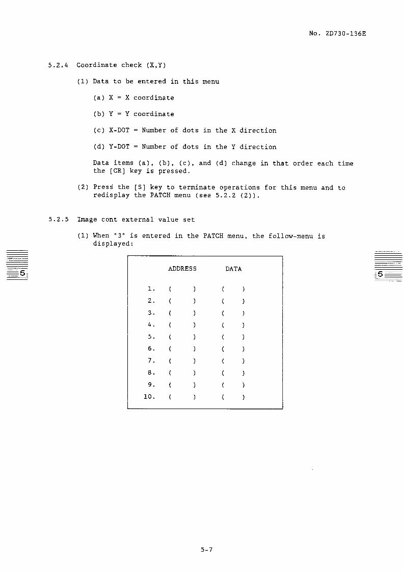
No. 2D730-136E
5.2.4 Coordinate check (X,Y)
(1) Data to be entered in this menu
(a) X = X coordinate
(W Y = Y coordinate
(c) X-DOT = Number of dots in the X direction
(d) Y-DOT = Number of dots in the Y direction
Data items (a), (b), (c), and (d) change in that order each time the [CR] key is pressed.
(2) Press the [S] key to terminate operations for this menu and to redisplay the PATCH menu (see 5.2.2 (2)).
5.2.5 Image cant external. value set
(1) When "3" is entered in the PATCH menu, the follow-menu is displayed:
1.
2.
3.
4.
5.
6.
7.
8.
9.
10.
ADDRESS
( >
( >
( 1
( >
( >
( >
( >
( >
( >
( >
DATA
( >
( >
( >
( 1
( >
( >
( >
( >
( >
( 1
5-7

No. 2D730-136E
(2) Functions of the other keys in this menu
(3)
(4)
(5)
(a) [ENTER] key
Press this key after entering an address and data.
(b) [DELI key
Press this key to delete all addresses and data.
(c) [SPACE] key
Press this key to delete one address and data value.
(d) [?I key
Press this key to move the cursor up (from 10 to 1).
(e) [Al key
Press this key to move the cursor down (from 1 to 10).
PATCH MENU display by KEY IN "S". (Return to the status in
5.2.2 (2).)
Data output timing
o IMAGE CONT EXTERNAL VALUE SET is selected in the PATCH menu.
Data is output before hardware-controlling I/O processing is performed.
("(PM3)" is displayed during execution of the program.)
Turn off the PATCH menu. The PATCH program starts.
Note: To terminate processing, call up the PATCH menu again.
5-8
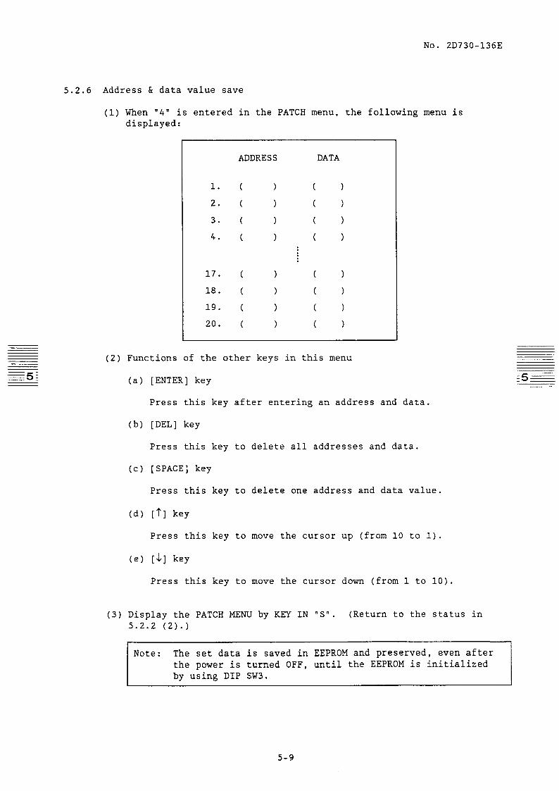
No. 2D730-136E
5.2.6 Address & data value save
(1) When "4" is entered in the PATCH menu, the following menu is displayed:
ADDRESS DATA
1.
2.
3.
4.
( >
( )
( 1
( 1
17. ( >
18. ( 1
19. ( >
20. ( >
( 1
( >
( 1
( > : : :
( >
( 1
( >
( 1
(2) Functions of the other keys in this menu
(a) [ENTER] key
Press this key after entering an address and data.
(b) [DEL] key
Press this key to delete all addresses and data.
(c) [SPACE] key
Press this key to delete one address and data value.
(d) [?I key
Press this key to move the cursor up (from 10 to 1).
(e) [J] key
Press this key to move the cursor down (from 1 to 10).
(3) Display the PATCH MENU by KEY IN "S". (Return to the status in
5.2.2 (2).)
Note: The set data is saved in EEPROM and preserved, even after the power is turned OFF, until the EEPROM is initialized
by using DIP SW3.
5-9

No. 2D730-136E
(4) Data output timing
l ADDRESS & DATA VALUE SAVE is selected in the PATCH menu.
Data is output after hardware-controlling I/O processing performed ("(PM4)" is displayed during execution of the program).
(5) Turn off the PATCH menu. The PATCH program starts.
is
I Note: To terminate processing, call_ up the PATCH menu again. I
S-10

TOSHIBA
TOSHIBA CORPORATION
1385,SHIMOISHIGAMI,OTAWARA-SHI,TOCHIGI-KEN 324-8550,JAPAN