new sled 3 system for multi-mega watt rf compressor chen
TRANSCRIPT
New SLED 3 system for Multi-mega Watt RF compressor
Chen Xu, Juwen Wang, Sami Tantawi
SLAC National Accelerator Laboratory, Stanford University, Stanford, CA 94309, USA Electronic address: [email protected]
Abstract
A compact X band SLED is introduced for X band RF compressing application. This SLED
compressor consists two major parts: a rectangular to circular waveguide converter and an overmoded
spherical cavity. The RF compressor is designed to convert 50 magawatt X band RF power with pulse
length 1.5 microseconds and deliver 200 megawatts with pulse length 106 nanoseconds to the X band
accelerating structure.
1. Introduction
SLAC has successfully designed and utilized X band and S band RF power compressor for NLC
project and LCLS project. SLED is named as SLAC's Energy Doubling accelerating gradient. The
conventional idea for SLED is that to store the first part energy of input RF pulse by cavities and releases
the stored energy in cavities along with the second part of the pulse. Since the pulse power phase has been
turned 180 degree, the output pulse is a combination in phase of the leakage power and input power. Thus,
the pulse power is compressed and increased. Compression ratio, namely, the duration ratio between
before and after compression is around 6. There are two critical points for this SLED technique: 1. The
cavities must be over-coupled in order to obtain a output power higher than the original input power. 2.
The pulse delivery network must be directional in order to combine leakage power and the flipped input
pulse. The schematic system is shown in fig.1.

Fig.1. schematic drawing of the SLED microwave network.
A 3db coupler is a four ports directional coupler. It is designed to convert a rectangular waveguide
TE10 mode to equally feed two cavities without leakage to the fourth ports in fig.2.
Fig.2. High power short slot hybrid 3db coupler.
Moreover, when the power is leaked from these two cavities, the power from port 2 and 3 are
canceling output to port 1 and combining output to port 4. This directional coupling characteristic is
essential for the SLED technique.
This conventional SLED utilized two single-moded pillbox cavities with quality factor around 105.
The cavity mode at 2.8GHz is TE015 mode. The mode has a pattern showing in fig.3. The mode has

Q~105 and coupling coefficient ( ~5), therefore, the loaded QL is
42 10 and mode bandwidth is
90KHz.
The whole structure is utilized in the current LCLS accelerator main linac, and it helps boosting the
LCLS accelerated electron energy from 6GeV to 12GeV. However, the two bulky cavities and a 3 db
coupler have size of 1.5 1.5 1.5m m m for S band operation. Our goal is reduce its size and increasing
the compression ratio to around 10. This goal yields higher compressed power and shorter output pulse
for X band operation.
2. Design concept
We recently design three versions of dual modes circular polarized couplers. These couplers can
convert TE10 rectangular waveguide into two TE11 modes with different polarization in a circular
waveguide. This over-moded structure can replace the conventional 3db couplers even though it only has
three physical ports. The over-moded output can feed an overmoded cavity to avoid the second cavity in
the conventional SLED design. Similarly, the modes inside this cavity will have the same , Q and
degeneration frequency.
An ideal candidate for this application is a spherical cavity. Spherical cavity has analytical solution
for TE and TM modes. A TEmnp or TMmnp modes are labelled for azimuthal, polar and radial directions.
The TEmnp field scalar potential is formulated in following. The field potential patterns are shown in Fig. 4.
The electromagnetic field for TEmnp can be derived the equation below :
22
2
2
2
0 ( )
1 1
sin
1 1
sin
r r r
r r
r r
E H k Fr
F FE H
r r r
F FE H
r r r
Fig.4. The electromagnetic field pattern for TE 114 mode.
Note these three modes have identical field pattern but different polarizations. In a spherical structure,
the mode orientation is determined by the excitation signal from a give port. For example, dipole input
feeds on the spherical cavity wall will coupling TE114 dipole modes. However, the TE014 cannot be
excited by any dipole mode in a circular waveguide, thus this TE014 would have very small coupling .
In order to avoid close neighbor modes and obtain higher Q0, TEn14 modes are chosen. In this Ten14
family, there are three degeneration modes: one TE014 and two TE114 modes. When spherical cavity
has a radius of 5.8749cm, the TEn14 family has a degeneration frequency of 11.424GHz and the Q0 is
around 105. We need to design a coupler to this spherical cavity, and make large enough to obtain the
maximum output. Assumed the traveling back wave accelerating structure to feed has a feeding time
around 100ns, the gradient reaches maximum when is around 9. The outputs of the circular polarizer
are from one circular waveguide, and each polarization mode in this waveguide is used to feed the
different modes in the spherical cavity. Two single mode cavities is replaced by two polarization in one
cavity, and spherical cavity and polarizer supple two modes and feeds with identical RF characteristics.
3. Characteristic of the dual circular polarizer and spherical ball design
3.1. Dual modes Circular converter
The polarizer has three physical ports but the output circular waveguide supports two modes. These
two TE11 modes have the same power magnitude, different polarization and 90 degree phase delay.
Using this two TE11 circular modes to feeds two TE114 modes in the cavity, the input power are split
into two cavity modes which canceling each other at the output rectangular waveguide. The scattering
matrix for this structure is shown below:

The electric field on the surface of this structure is shown in Fig. 4.
Fig.4: The complex magnitude of E field on coupler surface.
This structure has a fairly wide RF operation bandwidth. The output of this coupler is a TE11 circular
mode rotating on port 3. The frequency spectrum of scattering parameters is shown in Fig 5, and it
shows that the port 1 has neither reflection nor a transmission, and all power equally split into two modes
in port 3.

Fig.5. Scattering parameters frequency spectrum.
3.2. Spherical cavity design.
The radius of a spherical cavity is 5.8749cm when the resonating frequency is 11.424GHz. The
unloaded Q is 51 10 and an ideal goal is around 10. It is convenient to connect the spherical cavity
directly with the circular waveguide. An iris is introduced to control the coupling. The larger iris radius
will bring larger . While the operating frequency 11.424GHz is beyond the cutoff frequency of the
circular waveguide, the waveguide with an iris can cut off the 11.424GHz field within the iris region.
However, the thickness of this iris aperture is small, thus the evanescent TE11 mode can still couple into
the cavity. By optimizing this thin iris, one can obtain the coupling coefficient around 10. Fig.6 shows the
cavity E field on the surface of a given snapshot.
Fig.6 The snapshot of E field pattern at different frequency inside of the spherical cavity. Left is the
TE014 mode and right is one polarized TE114 mode.
The change of the iris radius can vary the coupling coefficient, because the leakage to the circular
waveguide is determined by the level of cutoff at the iris region. A larger iris can increase , but the
change is not a linear variation. Meanwhile, the TE114 resonating frequency is also change with change
of the iris radius. The scattering parameters are swept at different frequency in Fig. 7 and of each
resonating modes are calculated with different iris radius.
5.8mm

6.2mm

6.6mm
7mm
8mm

9.5mm
Fig.7. the scattering matrix and Smith chart of each frequency sweep.
Since the simulation from HFSS is in a steady state, one can extract of each iris radius setups
from the scattering parameter by the equation.
11
11
1
1
S
S
Smith charts are used to determine is under coupled or over coupled. The TE114 resonating
frequency, scattering matrix and the dependency with the iris radius are shown in Fig8.

nim
11.424
11.426
11.428
11.43
11.432
11.434
11.436
11.438
11.44
11.442
3 4 5 6 7 8 9 10
TE114 frequency vs Iris
-5
-4.5
-4
-3.5
-3
-2.5
-2
-1.5
-1
-0.5
0
3 4 5 6 7 8 9 10
Scattering vs Iris

Fig.8, The resonating frequency, scattering matrix and dependency with the change of the iris
radius.
3.3 Combination.
A copper sheet with thickness of 5mm is machined to this structure. The geometry of this SLED is
shown in Fig. 9. A snapshot of the surface E field is shown in Fig 10, and the input power from WR 90 is
1W. The peak E surface occurs at the waveguide, not on the surface of spherical cavity. When the input
power is 50MW, the peak surface E field is 8.63MV/m.
0
20
40
60
80
100
120
140
160
180
3 4 5 6 7 8 9 10
Beta vs Iris
Fig.9. the actual mechanical design of SLED system.
4. Frequency response, Transient response and Multi-physics concern.
4.1 Frequency response:

The cavity is simulated with frequency scan from GHz to GHz, and the frequency sweep is shown in
Fig.7. Smith chart is also plotted in the fig.10. The center resonating peak suggests the two TE114 modes
and the smaller peak on the right indicates the TE014 with very weak coupling. The TE114 modes have
two polarizations, and the fields’ patterns are identical except the orientation.
D
Fig.10: The scattering parameters scan of driving frequency.
4.2 Transient response:
Input pulse of this SLED compressor is a square pulse with a modulated rising time and at certain
time duration, the input pulse phase is flipped 180 degree. The pulse is both plotted in time domain and
frequency domain. The spectrum contains the center frequency and side band frequencies lobes and the
cavity resonates at the center frequencies. After convoluting the cavity spectrum in Fig 7 with input pulse
spectrum in fig.10, we inverse Fourier transform this output back to time domain and obtain an output
with a compressed pulse in fig 11.
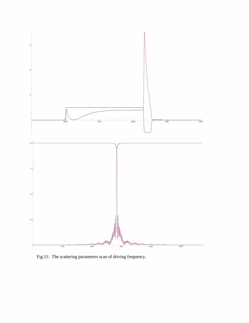
Fig.11: The scattering parameters scan of driving frequency.
5600 5700 5800 5900 6000
2
4
6
2000 4000 6000 8000 10000
0.5
1.0
1.5
2.0

5600 5700 5800 5900 6000
1.0
0.5
0.0
0.5
1.0

4.3 Thermal concern:
The SLED spherical cavity has fairly high Q0, thus the loss on the cavity wall is small compared with
the energy stored in the cavity. The major RF loss is from the waveguide, and the power loss on the
convertor and the system within a RF cycle is shown in Fig.12. The input power is normalized to 1W.
The integrated RF surface loss are W and W respectively.
2000 4000 6000 8000 10000
0.5
1.0
1.5
2.0
2000 4000 6000 8000 10000
0.5
1.0
1.5
2.0

Fig. 12. RF loss distribution on the converter and the system.
By using this RF loss as input load, ANSYS workbench is used to calculate temperature rise on the
copper internal surface. Note, the SLED is operated in a pulse mode, and the repetition rate of an X band
klystron is 120hz and duty factor is 0.18‰. This means the HFSS result which is a CW calculation needs
to multiply this duty factor to obtain averaged RF loss. A steady thermal calculation is simulated in
ANSYS. The temperature distribution on the internal surface is illustrated in Fig. 13.
Fig. 13. Temperature distribution on the system and the mode convertor.
4.4 Mechanical concern:
The cavity has two resonating modes and the total Q0 is the same as the individual Q0 because the
two modes are identical. The loaded Q is about one tenth of the Q0 and QL is around 104. The Lorentz
force on the cavity wall can be calculated locally with equation:
2 2
0surfaceP E H
The electric field acts as an attractive force and magnetic field acts a repulsively force. The
combination pressure on surface causes the deformation of the spherical cavity and leads to frequency
detuned. To avoid this, a mechanical enhancement is added to support the exterior. The force and
deformation on the surface are shown in the Fig. 14.

Fig .14. Surface force and deformation with input power 1W.
The detune frequency of spherical cavity is formulated in equation below:
0
0
m eU U
U
Assumed the is 10 and the input power is 50MW, and that make the power loss
2
4
1d fP P
on the wall is 16MW at steady state, thus the stored energy d LP QU
is around at 2.2 Joule at peak
charge. The typical coefficient to quantify this frequency tuning is Hz/(MV/m)2. As stated above, when
the ratio between max E surface field over input power is about 3500V/mW. Thus, the tuning coefficient
is Hz/W. We need a tuning range of MHz to operate 50MW on this SLED.
4.5 Tuning capability and Multipacting:
The cavity requires a tuning system to accurately adjust resonating frequency to 11.424GHz. As
stated above, the frequency will be tuned with stored energy, and we need a frequency tuner with a
frequency range around 20Mhz. A waveguide with a plunger can be an ideal tuner. One can use either a
circular waveguide with propagating or evanescent TE11 mode to tune this spherical cavity; however
both tuners have different frequency variation range and tuning sensitivity.
The setups of plunger tuners are demonstrated in Fig.15. A center rod with a stem is introduced to cut
off the TE11 coaxial mode in the pipe for both tuners. It is necessary to implement a choke joint structure
to prevent leakage in this coaxial for the propagating waveguide plunger. The space between two plates
in Fig15b, is this choke, and the distance in between is a quarter of waveguide wavelength in the choke
joint.
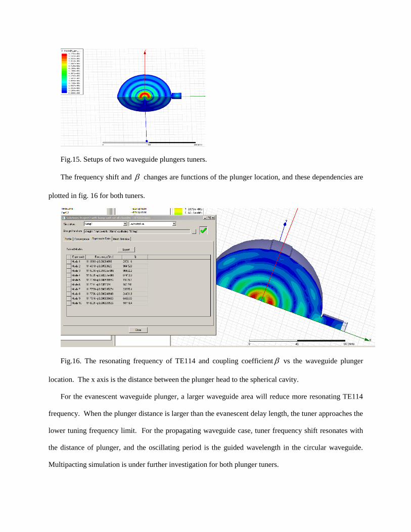
Fig.15. Setups of two waveguide plungers tuners.
The frequency shift and changes are functions of the plunger location, and these dependencies are
plotted in fig. 16 for both tuners.
Fig.16. The resonating frequency of TE114 and coupling coefficient vs the waveguide plunger
location. The x axis is the distance between the plunger head to the spherical cavity.
For the evanescent waveguide plunger, a larger waveguide area will reduce more resonating TE114
frequency. When the plunger distance is larger than the evanescent delay length, the tuner approaches the
lower tuning frequency limit. For the propagating waveguide case, tuner frequency shift resonates with
the distance of plunger, and the oscillating period is the guided wavelength in the circular waveguide.
Multipacting simulation is under further investigation for both plunger tuners.

5. Conclusion
A novel compact SLED is introduced and designed. The RF and multi-physics simulation suggests
that it can operate with input power of 50MW with pulse length of 1.5microseconds and output power of
150MW with pulse length 100ns. A prototype of this SLED is about to make and tested soon.
Acknowledgement
We would like to thank Dr David Farkas from SLAC national accelerating laboratory
for some useful discussions. This work was supported by Department of Energy Contract
No. DE-AC02-76SF00515.
Reference
1. H. Padamsee, J. Knobloch, and T. Hays, RF Superconductivity for Accelerators.
2nd Edition (Wiley and Sons, New York,NY, 2008).
2. W.-D. Moeller for the TESLA Collaboration, “High Power Coupler For The
TESLA Test Facility”, Proceedings of the 9th Workshop on the RF
Superconductivity, 1999, Santa Fe, V.2, pp.577-581.
3. J. R. Delayen, L.R. Doolittle, T. Hiatt, J. Hogan, J. Mammosser. “An R.F. Input
Coupler System For The CEBAF Energy Upgrade Cryomodule.” Proceedings of
the 1999 Particle Accelerator Conference, New York, 1999. pp1462-1464.
4. S. Belomestnykh, et al., “High Average Power Fundamental Input Couplers for
the Cornell University ERL: Requirements, Design Challenges and First Ideas,”
Cornell LEPP Report ERL 02-8 (September 9, 2002).
5. RF windows
6. E. Snitzer. “Cylindrical dielectric waveguide modes” Journal of the Optical
Society of America, Vol. 51, Issue 5, pp. 491-498 (1961)
7. Zaki, K.A. Atia, A.E. “Modes in Dielectric-Loaded Waveguides and Resonators. ”
Microwave Theory and Techniques, IEEE Transactions on V.31 , I.12 ,1982.
pp1039 – 1045.

8. Clarricoats, P.J.B .“Properties of dielectric-rod junctions in circular waveguide”,
Electrical Engineers, Proceedings of the Institution of (Volume:111 , Issue: 1 ).
1964. Pp.43 – 50
9. Clarricoats, P.J.B. ; Taylor, B.C. “Evanescent and propagating modes of
dielectric-loaded circular waveguide”. Electrical Engineers, Proceedings of the
Institution of (Volume:111 , Issue: 12 ) 1964 pp.1951-1956.
10. Walter M. Elsasser. “Attenuation in a Dielectric Circular Rod”. J. Appl. Phys. 20,
1193 (1949)
11. Rothwell, E.J. and Frasch, L.L. “Propagation characteristics of dielectric-rod-
loaded waveguides”.Microwave Theory and Techniques, IEEE Transactions
on (Volume:36 , Issue: 3 ) 1988. pp 594 – 600.
12. Optics book
13. S.F.Mahmoud. “Electromagnetics waveguides theory and applications”. The
Institution of Engineering and Technology (December 1991)
14. A.A. Mostafaa, C.M. Krowneb, K.A. Zakic & S. Tantawid “Hybrid-Mode Fields
in Isotropic and Anisotropic Planar Microstrip Structures.” Journal of
Electromagnetic Waves and Applications Volume 5, Issue 6, 1991
Appendix:

01 01
02 02
01 01
02 02
01 01 01
02 02 02
01 01 01
02 02 02
0
-Cos[ ] - e -Cos[ ] + e Sin[ ]0 0 0
2 2 2
-Cos[ ] - e -Cos[ ] + e Sin[ ]0 0 0
2 2 2
-Cos[ ] + e -Cos[ ] - e Sin[ ]0 0 0
2 2 2
-Cos[ ] + e -Cos[ ] - e Sin[ ]0 0 0
2 2 2
Sin[
i i
i i
i i
i iS
1 0101
02 0202
] Sin[ ]0 0 Cos[ ] 0
2 2
Sin[ ] Sin[ ]0 0 0 Cos[ ]
2 2
Table 5


5650 5700 5750 5800 5850 5900
1.0
0.5
0.5
1.0
1.5
2.0
5000 6000 7000 8000
0.5
1.0
1.5