new design proposals for high-power renewable … & solar power new design proposals for...
TRANSCRIPT

WIND & SOLAR POWERNew Design Proposals forHigh-Power Renewable Energy Applications
ISSUE 4 – June 2010 www.power-mag.com
Also inside this issueOpinion | Market News | PCIM 2010 Report | Renewable Energies: Solar Power | Wind Power | Products | Website Locator
01_PEE_0410_p01 Cover 03/06/2010 16:30 Page 1

02_PEE_0410_02_PEE_0410 03/06/2010 14:13 Page 1

CONTENTS
Power Electronics Europe Issue 4 2010 www.power-mag.com
3
Editor Achim Scharf
Tel: +49 (0)892865 9794
Fax: +49 (0)892800 132
Email: [email protected]
Production Editor Chris Davis
Tel: +44 (0)1732 370340
Financial Clare Jackson
Tel: +44 (0)1732 370340
Fax: +44 (0)1732 360034
Circulation Manager Anne Backers
Tel: +44 (0)208 647 3133
Fax: +44 (0)208 669 8013
Email: [email protected]
INTERNATIONAL SALES OFFICES
Mainland Europe:
Victoria Hufmann, Norbert Hufmann
Tel: +49 911 9397 643 Fax: +49 911 9397 6459
Email: [email protected]
Armin Wezel
Tel: +49 9568 897 097 Fax: +49 9568 897 096
Email: [email protected]
UK
Steve Regnier, Tim Anstee
Tel: +44 (0)1732 366555
email: [email protected]
Eastern US
Karen C Smith-Kernc
email: [email protected]
Western US and Canada
Alan A Kernc
Tel: +1 717 397 7100
Fax: +1 717 397 7800
email: [email protected]
Italy
Ferruccio Silvera
Tel: +39 022 846 716 Email: [email protected]
Taiwan
Prisco Ind. Service Corp.
Tel: 886 2 2322 5266 Fax: 886 2 2322 2205
Publisher Ian Atkinson
Tel: +44 (0)1732 370340
Fax: +44 (0)1732 360034
Email: [email protected]
www.power-mag.com
Circulation and subscription: Power ElectronicsEurope is available for the following subscriptioncharges. Power Electronics Europe: annual chargeUK/NI £60, overseas $130, EUR 120; single copiesUK/NI £10, overseas US$32, EUR 25. Contact: DFA Media, Cape House, 60a Priory Road, Tonbridge,Kent TN9 2BL Great Britain. Tel: +44 (0)1732 370340. Fax: +44 (0)1732360034. Refunds on cancelled subscriptions willonly be provided at the Publisher’s discretion, unlessspecifically guaranteed within the terms ofsubscription offer.
Editorial information should be sent to The Editor,Power Electronics Europe, PO Box 340131, 80098Munich, Germany.
The contents of Power Electronics Europe aresubject to reproduction in information storage andretrieval systems. All rights reserved. No part of thispublication may be reproduced in any form or by anymeans, electronic or mechanical includingphotocopying, recording or any information storageor retrieval system without the express prior writtenconsent of the publisher.Printed by: Garnett Dickinson.ISSN 1748-3530
PAGE 16
Three-Phase Two-HF-Switch PVInverter with Thyristor InterfaceTo feed-in an alternating current into the medium voltage AC grid several
requirements have to be kept. Next to rugged and interference-insusceptible
electronics, attention has to be given to the new grid connection guidelines in
Germany since 2008. Such new rules significantly affect the cost of inverters
nowadays, especially when usual semiconductor devices like IGBTs are employed.
This paper, awarded as best paper at PCIM 2010, deals with an inverter-topology
which combines the rugged properties of well known thyristor-circuits with the
features of modern inverters. Christian Nöding, Benjamin Sahan, Peter
Zacharias, Center of Competence for Distributed Power Technology
(KDEE), University of Kassel, Germany
PAGE 20
Power Semiconductor Technologiesfor Renewable Energy SourcesHigh power semiconductors are key components for controlling the generation
and connection to the network of renewable energy sources such as wind-
turbines and photovoltaic cells. For a highest efficiency of the energy source, it is
therefore essential to select the right device for the given conditions. This article
looks at the performance features for the available high power semiconductors of
choice and also takes a look at future device technologies and their expected
impact on efficiency. Björn Backlund and Munaf Rahimo, ABB Switzerland
Ltd, Semiconductors, Lenzburg, Switzerland
PAGE 28
GaN Power Devices for Micro InvertersGaN power products are set to have a direct impact on future efficient PV solar
inverter/converters. By reducing losses in each stage of the power conversion,
GaN based devices will help in increasing total energy harvesting. The integration
with driver ICs and other components will drive the size reduction and high
volume commerzialisation. Alberto Guerra and Jason Zhang, International
Rectifier, El Segundo, USA
PAGE 32
Transfer Mold IPM for PhotovoltaicApplicationA new low loss large Dual In-line Package Intelligent Power Module with rating of
50A/600V is designed for photovoltaic generation. It features a high heat
dissipating insulation sheet, 5th generation CSTBT IGBTs and high output current
driver IC leading to higher switching frequencies. Ming Shang, Hirofumi Oki,
Kazuhiro Kuriaki, Toru Iwagami, Toshiya Nakano, Power Device Works,
Mitsubishi Electric Corporation, Fukuoka-City, Japan
PAGE 37
Product Update A digest of the latest innovations and new product launches
PAGE 41
Website Product Locator
New Design Proposals forHigh-Power RenewableEnergy Applications Renewable energy applications are a great challengefor Power Electronics, with efficiency and reliabilitybeing the prevailing requirements. Today, 1700V low-voltage Silicon is vastly superior. For input/outputpowers of several MW, dozens of modules with dozensof chips need to be connected in parallel. The bestsolution is paralleling inverters / power blocks, butsuch solutions require additional low-voltagetransmission from the source to the medium-voltage(MV) transformer. An alternative solution is a MVsource and transmission connected to MV grid-sideinverter based on low-voltage Silicon - power blocks -connected in series. In addition, interleaved PWMreduces the size of the sinusoidal filter and theswitching frequency, as well as the total losses. Fullstory on page 24.
Cover supplied by SEMIKRON, Nuremberg, Germany
COVER STORY
PAGE 6
Market NewsPEE looks at the latest Market News and company
developments
PAGE 13
Back to GrowthPCIM Europe 2010 was held from May 4 - 6 in
Nuremberg and confirmed with an increase of 3% in
visitors (6300), 619 conference delegates and last
but not least 255 exhibitors its leading position
p03 Contents_p03 Contents 03/06/2010 16:05 Page 3

Core Components for Soft Starters
Broadest portfolio of SCR for Soft Starters Applications
� Isolated SCR modules from 1.2 kV up to 3.6 kV
� SCR Discs from 1.2 kV to >6.5 kV
� Current capability from 100A to >3000A
� Robust designs for highest performance and highest reliability
� Global sales and distribution network
� Excellent service and support
For further information please visit our website.
[ www.ifbip.com] ...for energy efficiency!
Infineon Technologies BipolarGmbH & Co. KG
04_PEE_0410_04_PEE_0410 03/06/2010 13:47 Page 1

OPINION 5
Power Electronics Europe Issue 4 2010 www.power-mag.com
The last time the global semiconductor industryachieved annual revenue growth greater than 30%was when the Dot-Com boom was hot. Now, 10years after the chip business’s whopping 37%expansion of 2000, according to market researcheriSuppli the industry is expected to finally break the30% barrier once again in 2010, with revenue set torise to $300 billion, up 30.6% from $230 billion in2009. Unlike the Internet-crazed spike in 2000,growth in chip sales this year will be driven by realfundamental supply/factors that slowly have beengaining momentum during the past 12 months.2010 is bringing a return to normal semiconductormarket conditions after the aberrant industryperformance in 2009, when chip sales plunged dueto external economic conditions. Compared to 2008,the semiconductor industry in 2010 will achievemore moderate revenue growth of 15.4%.
The power semiconductor market (discretes andpower modules) was worth $10.1 billion in 2009,declining by 24% from 2008 (power modulesdropped 26%, and discretes 24%). The market hasnot dropped by such a large extent since 2001,when it fell 22% because of the “Dot-Com” collapse.By end of 2010 a recovery up to $12 billion isexpected by IMS Research. EMEA’s powersemiconductor market fared little better in 2009, asthe European industrial markets finally plunged intothe downturn at the end of Q1 09; some countriesare still fighting their way out. This could explain whythe American power semiconductor marketoutperformed those of Japan and EMEA, as the USAwas one of the first countries to enter the globaldownturn and was one of the first countries out. TheSiC Schottky diode market was worth an estimated$29 million in 2009. It fell in line with the totalpower semiconductor market during the globaldownturn; but enjoyed strong demand in 2H 2009.Overall the SiC Schottky diode revenues wereestimated to be 25% higher in 2009 than in 2008.The SiC Schottky diode market will increase by over50% in 2010. PFC power supplies for server andtelecom applications currently account for the mostSiC Schottky diodes sold. The huge developments inthe Chinese telecom and cellular infrastructure, andhigh system-efficiency standards generally, are drivingtheir adoption. However, PV inverters could becomethe largest market for SiC Schottky diodes within thenext 3-4 years. Currently, SiC Schottky diodes are theonly SiC power devices sold in large volumes. SiC
JFETs are also available on the commercial marketbut have not yet succeeded to the same extent. IMSforecasts the SiC power semiconductor discrete andmodule market will be worth $110 million by 2012.Interestingly, the GaN power device market isprojected to be worth $20 million in 2012. Althoughthese GaN revenues are much lower than predictedby some other industry observers, they are muchhigher than SiC Schottky diodes achieved in their firstthree years on the market.
At PCIM 2010 all power semiconductor suppliersfelt enthusiastic about full manufacturing capacityloading, but on the other hand this situation leads tolong lead times of more than 28 weeks for smallerand around 12 weeks for larger orders i. e. for powerMOSFETs, according to market observers. Evenlonger lead times up to 40 weeks are announced forIGBTs. Thus power electronics system suppliers withtheir typical smaller orders are facing shortages incomponents supply and in consequence marketopportunities. Chinese power semiconductormanufacturers and their distributors such asAdvanced Power Electronics Corp. (www.a-powerusa.com) or Alpha Europe (www.alpha-europe.de) offer compatible products at competitivepricing and lower lead times in the range of 4 - 6weeks.
Another way to cope with long lead times isramping-up production capabilities, as TexasInstruments is demonstrating with the recentpurchase of more than 100 tools from formermemory maker Qimonda North America andQimonda Dresden, Germany. This is the first step inlaunching the Phase II expansion of RFAB, theindustry’s first 300mm analog/power wafer fab,located in Richardson, Texas. TI additionally invested$172.5 million to purchase this semiconductormanufacturing equipment at an opportune price.Phase II of RFAB will double the analogmanufacturing capacity in the North Texas facility,bringing its revenue capability to about $2 billion.First products qualified by end of 2010 are based onthe company’s LBC7 linear BiCMOS technologywhich is capable of integrating a variety ofcomponents, including power transistors (up to40V), CMOS logic, bipolar transistors and passives.Key benefits of LBC7 are low on-resistance, highcurrent carrying capabilities, high integration capabilityand extremely low leakage. With shipmentsbeginning by the end of the year, this phase IIexpansion will give TI a head start in providingcustomers access to significant analog capacity tofuel their growth, according to TI.
More on that and on PCIM at the following pages.
Achim ScharfPEE Editor
Good Times forPower SemiconductorSuppliers
- AUSTRIA DAU Ges.m.b.H. & Co. KG
Tel: +43 (0) 31 43 / 23 51 - 0 [email protected]
- USA DAU Thermal Solutions Inc.Phone: +1 519 954 0255
AIR COOLING
LIQUID COOLING
FOR CLAMPING TSINKSHEA
LIQUID COOLED AIR AND
ACKS)(STSYSTEMS
IR COOLING
stable construction for production process patented manufacturedwithout busbaravailable with and low thermal resistancehigh fin density design
AIR COOLING
high clamp force
.H. & Co. KGDAU Ges.m.b - AUSTRIA - AUSTRIA
high clamp forcestable construction for low thermal resistanceconnectorwith and without busbar semiconductors available nearly all sizes of disc several standard sizes for
.dau-at.com
.dauusa.com
0 - 1 523 / 43 1 3(0) el: +43 T.H. & Co. KGDAU Ges.m.b
25519 954 0Phone: +1 5DAU Thermal Solutions Inc.
- USA - USA
05_PEE_0410_NEW_p05 Opinion 03/06/2010 15:39 Page 5

By taking over the majority ofCompact Dynamics GmbH, adesigner for innovative electricaldrives and control systems,Semikron can now offerdevelopment competence frompower electronics to electricalmotors. Recently a new line of
Semikron Invests in Hybrid and Electric Vehicles
6 MARKET NEWS
Issue 4 2010 Power Electronics Europe www.power-mag.com
converters for special (H)EVs wasintroduced.The company’s aim is to develop
high efficiency, light-weight andcompact systems in order to meetthe ever increasing demand for
highly compact drives combiningstate-of-the-art power electronicsand control systems. The drivesystems are optimized for use inhybrid and electric vehicles such ascars, busse s and utility vehicles, aswell as construction, forest,agricultural systems and forklifttrucks. “We complement each otherperfectly, both our companies havelong ranging experience in powerelectronic systems”, said Semikron’sCEO Dirk Heidenreich. “Together,we integrate the technology ofelectrical motors, control electronicsand power electronics to offerhighly efficient, compact and light-weight driv e systems to vehiclemanufacturers”, added MaximilianEck, General Manager of CompactDynamics. Compact Dynamicsspecializes in the development andprototyping of electric drivesystems with a particular focus onautomotive applications includinghigh-power electric drives for motorsport applications. Following thejoint venture with Magna in June2009 and the launch of the newSemikron SKAI2 IGBTs andMOSFE T systems for hybrid andelectric vehicles in May 2010, thisinvestment is another step into themarket for electro-mobility.SKAI systems are developed in
line with the latest automotivestandards and are supplied asstandard modules with low-voltageMOSFETs, high-voltage IGBTs or
with the topology of single, dualand multiple inverters. SKAIsystems are also developed tomeet individual customerspecificatio ns. All SKAI 2 modulesare fully qualified using analysissuch as highly-accelerated lifetesting (HALT) and end ofcomponent-life testing, with fullfailure-mode effect analysis studiesconducted at all critical points ofthe design cycle, to ensure thatthey are in line with relevantautomotive standards.The high-voltage SKAI 2 is a
water-cooled 600/1200V IGBTinverter system, and has beenoptimised for use in applicationssuch as full-electric cars, plug-inhybrid cars and electric buses. Thissystem is based on the sintered,solder-free SKiM93 IGBT modulesand a polypropylene film DC-linkcapacitor, driver electronics, alatest-generation DSP controller,EMC filters, and current, voltageand temperature sensors, andcomes in an IP67 module case.Communication with the vehiclemaster controller is via a CAN bu s.These systems are designed foroutputs of up to 250kVA. The low-voltage SKAI 2 is an air-cooled orwater-cooled 50/100/150/200VMOSFET single and dual invertersystem that is used mainly in fork-lift trucks and other materials-handling applications suitable formotor output of up to 55 kVA. They
incorporate many of the samefeatures as the IGBT-basedsystems. The third type of SKAI 2platform is a multi-converter boxalso housed in water-cooled, IP67-protected case. The signal interfacefeatures analog and digital I/Os toallow for the connection of a wide
variety of sensors, such astemperature sensors and resolverinputs. A typical multi-convertersystem would include a three-phase 40kVA active f ront-endconverter, a three-phase 20kVAdrive inverter, a three-phase 10kVAdrive inverter, and a 14V/300A or28V/165A DC/DC converter.“Our SKAI products are complete
converters exclusive software andcan be used for all wheel-equippedvehicles”, commented PeterBeckedahl, Semikron’s ManagerConcepts & Application. “The low-voltage SKAI2 is equipped with SJMOSFETs from Infineon and Vishay,for the high-volt age version we useIGBTs from ABB, Fuji and Infineon.We do not address the massmarket, typical units are in therange of 1000”.
www.semikron.com
By taking over the majority of CompactDynamics Semikron’s CEO DirkHeidenreich takes another step towardselectro-mobility
“With SKAI we offer complete convertersexclusive software which can be used forall wheel-equipped vehicles”, commentedSemikron’s Manager Concepts &Application Peter Beckedahl
SKAI2 parameters and applications
Market News_Layout 1 03/06/2010 13:51 Page 6

���������
National Technology Park, Ashling Building, Limerick, Ireland • 353-61-504300 • www.ar-europe.ieCopyright © 2010 AR. The orange stripe on AR products is Reg. U.S. Pat. & TM. Off.
A Partnership Where Everyone Benefits.
One exists for the other. It’s profoundly simple. And powerfully successful. At AR Europe, we supply power amplifiers, antennas, and modules for EMC testing, wireless,medical and industrial applications. Over the last 40 years, we’ve learned some important lessonsabout partnerships. Our partners have taught us that when you set your standards (and your sights) high, there’s no telling how far you can go. We’ve learned that when you meet people more than half way, they usually do the same. We’ve learned that a company is only as strong as it’s weakest link. Which is why we forge al-liances with only the best in the field. Most important, partnerships teach us that success is more than just sharing products. It’s sharingresources. Lending a hand. And maybe an ear once in a while. It’s the difference between a partnership that withers, and one that really takes off. If that’s youridea of a mutually beneficial relationship, we invite you to explore one with AR.
Contact Enda Murphy [email protected]. or call 353-61-504300
AR BeneluxTel: 31-172-423-000BelgiumLuxembourgNetherlands
AR FranceTel: 33-1-47-91-75-30France
AR United Kingdom Ltd.Tel: 441-908-282766IrelandUnited Kingdom
Caltest OyTel: 358-9-530-6070EstoniaFinlandLatviaLithuania
CE-BIT Elektronik ABTel: 46-8-7357550Sweden
Emitec AGTel: 41-41-748-6010Switzerland
EMV GmbhTel: 49-89-614-1710AustriaGermany
Erik BlichfeldTel: 45-7552-2020�������
H TESTTel: 420-235365207�$������� ����� ����#���!����
Nortelco ElectronicsTel: 47-22-57-6100��"�#
ORKOTel: 90-312-438-2213 ���#
Radiant-ElcomTel: 7495-725-0404����� �� �����������
Teseo S.p.A.Tel: 39-011-994-1911����#
Urzadzenia Elektroniczne ImportTel: 022-313-17-35 �����
Vector Technologies Ltd.Tel: 30-210-6858008�������� ��������������#�� ��������������������������������!����
Wavecontrol, S.L.Tel: 34-933-208-055��� ��������
07_PEE_0410_07_PEE_0410 03/06/2010 14:12 Page 1

8 MARKET NEWS
Issue 4 2010 Power Electronics Europe www.power-mag.com
300 Millimeter Fab for Analog and PowerTexas Instruments is expanding itsanalog/power manufacturingcapacity with the recent purchase ofmore than 100 tools from formermemory maker Qimonda NorthAmerica and Qimonda Dresden,Germany. This is the first step inlaunching the Phase II expansion ofRFAB, the industry’s first 300mmanalog wafer fab, located inRichardson, Texas, near TI’sheadquarters. Texas Instruments’ latest US-based
manufacturing facility (RFAB) wascompleted in 2006. Since that time,the company has weathered theeconomic downturn and focused itsbusiness on analog and embeddedprocessing, while watching marketdemand to determine when to equip
and open the facility. This productionstrategy has enabled the company toramp up production when conditionscall for increased production.The RFAB project began with
ambitious goals regarding cost,energy and the environment, andrequired rethinking every aspect ofthe design. TI engineers spent timewith experts from the RockyMountain Institute to create anextremely efficient complex unlikeany other semiconductor facility. Itsenergy-saving features will enable35% more efficiency than coderequirements, which will help reducerelated emissions by 50%. Waterconversation efforts, including re-useand recycling, will reduce waterconsumption by 40%. In total, TI
spent about $1.5 million of its $320million construction costs onsustainable design. In return, thecompany expects to see a milliondollars of savings in the first year ofproduction, ramping up to more than$4 million a year once the factory isfully operational.TI additionally invested $172.5
million to purchase semiconductormanufacturing equipment at anopportune price from bankruptQimonda. Phase II of RFAB willdouble the analog manufacturingcapacity in the North Texas facility,bringing its revenue capability toabout $2 billion. The fab will produceanalog ICs based on TI’s proprietaryprocesses. First products qualified byend of 2010 are based on the
company’s LBC7 linear BiCMOStechnology which is capable ofintegrating a variety of components,including power transistors (up to40V), CMOS logic, bipolar transistorsand passives. Key benefits of LBC7are low on-resistance, high currentcarrying capabilities, high integrationcapability and extremely low leakage.“Our 300mm fab is a uniquecornerstone of our analog business.With phase I progressing well and ontrack to begin shipments by the endof the year, this phase II expansionwill give us a head start in providingour customers access to significantanalog capacity to fuel their growth,”said TI’s SVP Gregg Lowe.
www.ti.com
TI’s new RFAB in Richardson/Texas incorporating 300mm wafer manufacturing equipment for analog and power semiconductors
Market News_Layout 1 03/06/2010 13:52 Page 8

Next generation inverter designs for renewable energy applications demand
reliable DC link capacitors with higher capacitance values, voltage, and cur-
rent ratings. Now available in new case sizes, Cornell Dubilier’s expanded
range of Type 947C power � lm capacitors meet or exceed the requirements
for bulk energy storage, ripple � ltering and life expectancy for wind and
solar power inverter designs, as well as electric vehicle applications. Select
from hundreds of standard catalog listings, or connect with CDE engineers to
develop special designs to your requirements.
For sample requests or more technical information, visit www.cde.com/pe
C A PAC I TO R S O L U T I O N S F O R P OW E R E L E C T R O N I C S
TYPE 947C POWER FILM CAPACITORS
85, 90 & 116 mm CASE SIZES
CAPACITANCE VALUES TO 1500 µF
APPLIED VOLTAGE TO 1300 Vdc
RIPPLE CURRENT RATINGS TO 100 Arms
M O R E O P T I O N S F O R P O W E R E L E C T R O N I C S
09_PEE_0410_09_PEE_0410 03/06/2010 16:13 Page 1

10 MARKET NEWS
Issue 4 2010 Power Electronics Europe www.power-mag.com
Higher Power Density for DC/DC ConvertersPicor, a subsidiary of VicorCorporation specialising inthe design and developmentof high performance powermanagement solutions,announces surface-mountisolated DC/DC convertersdelivering 3-4 times morepower density than existingsolutions.Vicor’s revenues for the
first fiscal quarter endedMarch 31, 2010, increased to$51,709,000, compared to$50,448,000 for thecorresponding period a yearago, and increased from$49,138,000 for the fourthquarter of 2009. “Each of ourthree primary business unitsexperienced improvedbookings and revenue.Consolidated revenueincreased 5.2% sequentially,while the consolidated book-to-bill ratio for the firstquarter was 1.39:1, ascompared to 1.16:1 for thefourth quarter of 2009 . Totalbacklog at the end of thefirst quarter of 2010 was$78,407,000, as compared to$58,489,000 at the end of2009”, said CEO PatrizioVinciarelli. “Our brickcomponents business grewsequentially, with particularstrength in its configurableproduct lines. V-I Chiprevenue for the first quartergrew 99% sequentially, whilebookings grew at a fasterpace as a large customerplaced initial productionorders for new programs. V-IChip also received initialorders from other earlyadopters of FactorizedPower. With increasedvolume, we expect to achieveimprovement in product-level profitability, althoughwe do not expect to reachour efficiency and margintargets in 2010. Picor alsogrew sequentially and
experienced strong bookings.Picor is collaborating closelywith V-I Chip in providingpower managementsolutions and, in particular,is sharing in V-I Chip’ssuccess with important earlyadopters.” Picor as a relatively new
subsidary is focusing onSilicon solutions contributingwith single digit share forVicor’s power modulesbusiness. “Besides Silicon weare looking for the featuresof the upcoming GaN powerdevices”, said Carl Smith,Director Strategic Marketing& Business Development.“Next generation ASICs,DSPs, FPGAs and high-speed
microprocessors areconstantly evolving to enableenhanced systemperformance. But it’s not allabout the processor!Improvements are requiredin component technologyand packaging concepts inall areas of the system tokeep pace with system-levelgoals. Next generationprocessors demand higherpower requirements, morevoltage rails, while leavingless aggregate real estate forthe power convers ionsolutions. Even thoughmaybe not obvious to theend-system designer, thechoice of power conversionsolution & power
architecture is a technologyenabling decision. Thus ourCool-Power high-densityisolated DC-DC convertertechnology was developedfor end-systems such asadvanced telecom andwireless infrastructure,networking &communications, Power-over-Ethernet applicationsand high speed serverplatforms. The PI3101 is thefirst in a new family of high-density power conversionproducts that leverages thecompany’s core strength inpower management, siliconintegration and system-levelpackaging.”The Cool-Power family is
built on a proprietary ZVStopology with planarmagnetics enablingswitching frequencies inexcess of 1MHz with up to87% efficiency. Delivering aregulated 3.3V output at upto 18A output curren t, from awide input voltage range of36V to 75VDC, the PI3101achieves 25W/cm3
(400W/in3), representing 3-4times the power density ofexisting solutions, andoptimises board area byproviding 16.5W/cm2
(105W/in2). The PI3101combines isolation, voltagetransformation and outputregulation into a highdensity, surface-mountPower-System-in-Package(PSiP) platform with a tinyfootprint 3.6cm2 (0.57in2) andvery low profile 6.7mm(0.27in). “This equals to halfof the size of a sixteenthbrick” Smith stated.
www.picorpower.com
Picor’s Carl Smith showing anevaluation board for the company’snew Cool-Power device
Market News_Layout 1 03/06/2010 13:52 Page 10

MARKET NEWS 11
www.power-mag.com Issue 4 2010 Power Electronics Europe
Highest Annual Growth in 10Years for SemiconductorsThe last time the globalsemiconductor industry achievedannual revenue growth greater than30% was when the Dot-Com boomwas hot. Now, 10 years after the chipbusiness’s whopping 37% expansionof 2000, the industry is expected tofinally break the 30% barrier onceagain in 2010, with revenue set torise to $300 billion, up 30.6% from$230 billion in 2009.However, unlike the Internet-crazed
spike in 2000, growth in chip salesthis year will be driven by realfundamental supply/factors that slowlyhave been gaining momentum duringthe past 12 months. “Building on thecontinuing expansion in sales thatfollowed the downturn in late 2008and early 2009, the semiconductorindustry is set to achieve remarkablerevenue growth and record size in2010,” said iSuppli’s analyst Dale Ford.“Chip sales growth this year will befueled by a number of key factors,including continued strong consumerdemand for hot electronic products,diligent inventory and capacitymanagement efforts among chipmakers and the arrival of innovativetechnologies at both the componentand end-system levels.”This year will mark an all-time
annual high for global semiconductorrevenue, eclipsing the previous recordof $274 billion set in 2007 by about9%. Ford noted that 2010 is bringinga return to normal semiconductormarket conditions after the aberrantindustry performance in 2009, whenchip sales plunged due to externaleconomic conditions. “While thegrowth in 2010 is impressive, it stillneeds to be viewed in context of the
dismal results in 2009. Compared to2008, the semiconductor industry in2010 will achieve more moderaterevenue growth of 15.4%.”The stage for strong annual growth
in 2010 was set by unusually robustconditions in the first quarter.“Semiconductor sales mostcommonly decline in the seasonallyslow first quarter compared to thepeak holiday period in the fourthquarter. However, in 2010, first-quarter chip sales expanded by 1.1%compared to the fourth quarter of2009. This is the first time theindustry has achieved sequentialgrowth in the first quarter since 2004,
and it represents the strongest growthduring the period since 2002, whenrevenue grew by 5.4%”, Fordobserved. A major factor driving demand in
the first quarter and beyond isconsumer demand for electronicproducts, which continues to surpassexpectations. Strong sales growth ispredicted for 2010 in PCs, mobile
handsets, LCD-TVs and othersemiconductor-rich electronicsystems. This will propel global factoryrevenue for electronic systems to arecord high of $1.55 trillion in 2010,up 10.4% from $1.4 trillion in 2008.The previous high for electronic OEMrevenue was $1.53 trillion in 2008.Overall electronic equipment
demand is being boosted by thehealth of the overall economy. “Theeconomy represents the biggest wildcard in our 2010 forecast,” Fordwarned. “While many indicators haveshown sustained improvement, thereare, however, a number of financialand economic trouble spots that
semiconductor companies have beenable to hold supplies at levels lessthan demand. As a result, manysemiconductor product segments areexperiencing strong upward pricepressure”, Ford said. Dramatic growth in DRAM revenues
will be a major driver of growth in theoverall semiconductor market. DRAMrevenue growth in 2010 is projectedto reach nearly 77%. Other major growth drivers in 2010
will be NAND flash memory, analogICs, discretes, LEDs andProgrammable Logic Devices (PLDs).All of these major market segmentsare forecasted to attain growth of
could endanger the continued growthin the market before the end of2010.” Beyond strong demand,
semiconductor suppliers also arebenefitting from careful managementof chip inventories and tight controlson manufacturing capacity.“By keeping a tight reign on
stockpiles and production,
more than 30% during the year. Mostof the significant product segmentsare expected to expand by more than20%.According to market researcher
Gartner total worldwidesemiconductor revenue reached$228.4 billion in 2009, down $26.8billion, or 10.5%, from 2008. Intelheld the No. 1 position ($33.253billion) for the 18th consecutive year.It increased its market share to 14.6%in 2009 from 13.6% despite itsrevenue declining $1.6 billion. Thisperformance was primarily due to therelative strength of the PC market,mobiles in particular, which sold welldespite the recession. With a hugegap (7.7% market share) Samsungwas second, followed by Toshiba(4.2%).
www.isuppli.comwww.gartner.comForecast of annual global semiconductor revenue growth Source: iSuppli
Forecast of quarterly global semiconductor revenue growth Source: iSuppli
Market News_Layout 1 03/06/2010 13:52 Page 11

12 MARKET NEWS
Issue 4 2010 Power Electronics Europe www.power-mag.com
The power semiconductor market wasworth $10.1 billion in 2009, decliningby 24% from 2008 (power modulesdropped 26%, and discretes 24%).The market has not dropped by such alarge extent since 2001, when it fell22% because of the “Dot-Com”collapse. By end of 2010 a recovery upto $12 billion is expected by IMSResearch. The Japanese powersemiconductor market was the worsthit in 2009, falling from $3.2 billion to$2.1 billion. However, the JapaneseYen dropped 10% against the US $,which accounts for some of the fall.Indeed, some Japanese power modulesuppliers reported customer ordersdropping by 50-60% in 2009, in theinduction heating and welding andcommercial HVAC sectors. EMEA’s power semiconductor
market fared little better in 2009, asthe European industrial markets finallyplunged into the downturn at the endof Q1 09; some countries are stillfighting their way out. This couldexplain why the American powersemiconductor market outperformedthose of Japan and EMEA, as the USAwas one of the first countries to enterthe global downturn and was one ofthe first countries out.Infineon Technologies was
estimated to have increased its powersemiconductor market share to 11.7%in 2009 and remained the largestsupplier to the market for the seventhconsecutive year. Toshiba leapfroggedFairchild, STMicroelectronics andVishay, which followed in that order.These leading five suppliers wereestimated to account for almost 40%
of the total 2009 market. The discrete power semiconductor
market was worth $8.1 billion in 2009.Power MOSFETs and power rectifierstogether accounted for 74% of thetotal revenues; revenues of eachdeclined by over 25%. MOSFETs sawthe largest decline, falling by nearly40%, though this is not surprising asover 95% of their market is theautomotive sector. The supplierrankings for the discrete powersemiconductor market saw animportant change in 2009: Toshibamoved from 5th place in 2008 to 1stin 2009. “Toshiba performed incrediblyin 2009 considering the economicsituation at the beginning of the year.One of the many reasons for Toshiba’sstrong performance was its largecustomer base in rest of Asia. Thediscrete power semiconductor marketin the rest of Asia fell by only 5% to15% depending on the devicecategory”, commented Josh Flood,market analyst at IMS Research.
As for power modules, thethyristor/diode module marketdropped by 30% in 2009, because ofthe induction welding and heatingmarkets being severely hit during theeconomic downturn. Sales of standardIGBT modules remained the mostrobust of the other power moduletypes. This can be attributed to theiruse in the renewable energy markets,such as wind and PV generation, whichwere less ruthlessly hit. Many industryobservers believe the market for highpower industrial motor drives copedbetter than that for low power drives,though opinions still differ. The top fourpower module suppliers - MitsubishiElectric, Infineon, Semikron, and FujiElectric in that order - remainedunchanged in 2009.
Silicon Carbide comes goodThe SiC Schottky diode market wasworth an estimated $29 million in2009. It fell in line with the total powersemiconductor market during theglobal downturn; but enjoyed strongdemand in 2H 2009. Overall the SiCSchottky diode revenues wereestimated to be 25% higher in 2009than in 2008. The SiC Schottky diodemarket will increase by over 50% in2010. PFC power supplies for serverand telecom applications currentlyaccount for the most SiC Schottkydiodes sold. The huge developmentsin the Chinese telecom and cellularinfrastructure, and high system-efficiency standards generally, aredriving their adoption. However, manyindustry experts believe PV inverterscould become the largest market for
SiC Schottky diodes within the next 3-4years, depending on the growth of thePV inverter market. “Currently, SiC Schottky diodes are
the only SiC power devices sold inlarge volumes. SiC JFETs are alsoavailable on the commercial marketbut have not yet succeeded to thesame extent. However, Cree are set tointroduce the SiC MOSFET this year,Transic will be releasing its SiC BJTs in2H 2010, and Infineon will releases itsSiC JFET in 2011; thus SiC powerdevices look very promising for thefuture”, Flood predicts. IMS forecaststhe SiC power semiconductor discreteand module market will be worth $110million by 2012. Interestingly, the GaNpower device market is projected to beworth $20 million in 2012. Althoughthese GaN revenues are much lowerthan predicted by some other industryobservers, they are much higher thanSiC Schottky diodes achieved in theirfirst three years on the market.The PV inverter market raced out of
2009, with record shipments of morethan 8 GW, 30% more than 2008.“Q4’09 saw huge demand for all PVproducts as investors rushed tocomplete systems before feed in tariffswere reduced in many key Europeanmarkets. 2.3 GW of installations werecompleted in Germany alone,”commented IMS analyst SamWilkinson. “This incredible demandresulted in 3.5 GW of inverters beingshipped worldwide in the final quarter.Demand has remained high into 2010and we now see a complete contrast tothe first half of last year with a shortageof components limiting the market,rather than weak demand”. SMA SolarTechnology (Germany) remained thelargest supplier of PV inverters in 2009and increased its share of shipments toan estimated 42%. FroniusInternational remained the secondlargest supplier worldwide and KacoNew Energy maintained its position asthird largest. The competitive landscapechanged somewhat more below thesesuppliers with Power-One and SputnikEngineering emerging as winners,surpassing several suppliers to becomethe fourth and fifth largest in 2009.
www.imsresearch.com
Power Semiconductor MarketRebound in 2010
World market for power semiconductor discretes and modules 2006 - 2010 Source: IMS Research
World power semiconductor supplier market share estimates Source: IMS Research
Market News_Layout 1 03/06/2010 13:52 Page 12

www.pcim.de PCIM 2010 13
www.power-mag.com Issue 4 2010 Power Electronics Europe
Back to GrowthPCIM Europe 2010 was held from May 4 - 6 in Nuremberg and confirmed with an increase of 3% invisitors (6300), 619 conference delegates and last but not least 255 exhibitors its leading position.
The majority of internationalexhibitors came from the USA,followed by Italy, Great Britain andFrance. The number of Asiancompanies was on the rise. As wellas the major players, many aspiringyoung companies were present. ThePCIM Conference encouraged anintensive dialogue between scienceand industry. 170 previouslyunpublished papers have been orallypresented over the three days. In 22presentations and 2 poster sessions,the latest developments have beendiscussed with the conferencedelegates.
Awards for outstanding papersThe conference focused on solarpower, in particular the awardedpapers and PEE’s Special Session.Again this year three Young
Engineer Awards (€1000.00 each)were presented to exceptionalcontributions from youngprofessionals (under 35 years old).The papers were selected by theConference Directors from morethan 100 papers and sponsored byECPE, Infineon Technologies andInternational Rectifier. Dayana El Hage, EPFL,
Switzerland, was awarded for the
paper “A high current pulse-powersupply for flash lamps in PV-panelmeasurement-facilities”.A high current pulse power supply
for the feeding of a flash lamp hasbeen developed, on the base of amultilevel converter with cascadedcells. The pulsed high power isprovided by capacitive energystorage, directly connected to thecells of the converter. A low currentripple is reached by interleavedswitching technique. The originaltopology, its design regarding thesizing of the storage cells, and theassociated control were presented.Christoph Klarenbach, UAS
Cologne, Germany, was the secondawardee with the paper “Fast andhigh precision motor control for highperformance servo drives”.He presented a new architecture
of a fast current controller with twofeedback signals for highperformance motion control. Due toparallel processing inside the FieldProgrammable Gate Array (FPGA),the control algorithm computing timeis significantly less than 1µs.Together with advanced controltechnologies in combination with anew current observer the bandwidthof fast switching IGBT or MOSFET
power stages is not limited by thedelay time of high precision(integrating) current measurementany longer. Using that technologyhigh control bandwidth inconjunction with high precisioncurrent control is now possible at notrade off. The control strategy relieson a simplified machine modelwithout incurring performancedegradations. The presented resultshave been produced with a highspeed Computerized NumericalControlled (CNC) machine (highspeed lathe).Andreas Munding, Liebherr-
Elektronik GmbH, Germany, won theprice for “Compact PCB-packagingand water cooling of a 25-kWinverter”. This work featured simulation
results of a sandwich PCB assemblywith an electronic board and a highcurrent board attached to either sideof an aluminum heat sink. This heatsink is thermally attached to themetal housing and to a liquid coolingchannel which was optimized for lowpressure drop. In addition, the effectof the low pressure drop coolerstructure on the IGBTs of a directlycooled pin-fin based power modulewas simulated and characterized. It
was found that a geometry withlateral coolant impingement exhibitlowest pressure drop and allows fora large flow rate operation range inautomotive applications.The determining criteria for the
Best Paper Award (a PEE-sponsoredpaid trip to PCIM China 2011 inShanghai) were originality, topicalityand quality. Christian Nöding fromUniversity of Kassel, Germany, wonthis price for the paper “Evaluation ofa Three-Phase Two-HF-Switch PVInverter with Thyristor-Interface andActive Power Factor Control”. Thecertificate was handed over by PCIMOrganizer Udo Weller and PEE EditorAchim Scharf on the PCIM 2010opening ceremony A short versionof this paper is published in ourfeature section.For the third time time Power
Electronics Europe has organised aSpecial Session with this year’s focuson Renewable Energy Applicationsfeaturing papers from BjörnBacklund, ABB Switzerland Ltd;Dejan Schreiber, SEMIKRONElektronik (Germany); AlbertoGuerra, International Rectifier (USA)and Shang Ming, Mitsubishi ElectricCorporation (Japan). These paperscan also be found in the featuresection of this issue.
New products and servicesABB Switzerland Ltd, Semiconductorsstarts mass production of 4.5kVSPT+ IGBT modules after successfulqualification and proven ramp-upphase in the traction market.“Our 4.5kV HV-HiPak2 IGBT
modules employ the wellestablished SPT+ IGBT and diodetechnologies. These modules havesignificantly lower conduction andswitching losses while exhibitinghigher SOA capability whencompared to the previousgeneration”, commented Sven Klaka,ABB’s VP Technology & ProductManagement. The SPT+ platform exploits an
Best paper awardee Christian Nöding(middle), PEE Editor Achim Scharf (left)and PCIM Organizer Udo Weller (right) atthe PCIM 2010 opening ceremony
PCIM_0410_Layout 1 03/06/2010 14:01 Page 13

14 PCIM 2010 www.pcim.de
Issue 4 2010 Power Electronics Europe www.power-mag.com
enhanced carrier profile throughplanar cell optimization, which iscompatible with ABB’s cell design.The on-state losses of the new 4.5kVIGBT exhibit approximately a 30%
reduction as compared to thestandard SPT device while keepingthe same Eoff value. For the 1200Arated Hipak2 module the typical on-state voltage drop at nominal currentand Tj=125°C is 3.55V. For the samemodule the typical turn-off switchingenergy (Eoff) at 2800 Vcc andTj=125°C is 6J. The new 4.5kV HV-HiPak2 modules will provide highvoltage system designers withenhanced current ratings andsimplified cooling while furtherenhancing the recently acquiredrobustness of the SPT IGBTs. ABB’s4.5kV modules are available incurrent ratings ranging from 650A -1200A in single IGBT as well asdiode configurations.www.abb.com/semiconductors
Avago introduced three MiniaturePrecision Isolation Amplifiers withincreased accuracy, bandwidth andhigh insulation made possible byproprietary optical isolation. Widelyused for motor phase and rail currentsensing, servo motor drive, switchingpower supply feedback isolation, DClink voltage monitoring, inverter currentsensing and switching power supplyfeedback isolation, the ACPL-C97xtargets industrial automation andinstrumentation, renewable energy,and HVAC markets. In a typical motordrive application, currents through asmall value current sense resistorcause a voltage drop that is sensed bythe ACPL-C79x isolation amplifier anda differential output voltage,proportional to the current, is createdon the output side of the isolationbarrier. Based on sigma-delta analog-to-digital converters and chopperstabilized amplifiers, the new isolationamplifiers feature high gain accuracy,low temperature drift, 3.3 V/5 Voutput supply operation and a wide -40 to +105°C operating temperaturerange. These features are delivered ina stretched SO-8 package that has afootprint 30% smaller than thestandard DIP-8 package. “Whenmounted on a PCB, it occupies aspace that is a fraction of that for atraditional Hall Effect or transformerbased isolation amplifier. The highcommon-mode transient immunity of15kV/µs provides the precision andstability needed to accurately monitorcurrent in high noise motor controlenvironments. This ensures smoothercontrol with less torque ripple in manymotor control applications”,commented Erik Halvordsson, Avago’sEuropean Business DevelopmentManager. www.avagotech.com/optocoupler
Cree announced the firstcommercially available 1700V SiCJunction Barrier Schottky (JBS)diodes targeted at high-voltageapplications in motor drive, windenergy and traction.
Initial products in the 1700Vseries include 10A and 25A JBSdiodes in die form, ready forintegration into 1700V powermodules ranging from 50 to 600A.“The 1700V diodes extend ouroffering in energy-efficient powersystems for datacenter and solarpower to new markets such as windenergy, train, tram and electricvehicle power converters,” saidCengiz Balkas, General ManagerPower and RF. “The advantages ofSilicon Carbide are clear, and forhigh-voltage, high-frequencysystems, you can’t afford not to useSiC.”www.cree.com/power
Dongbu HiTek from Seoul/Koreaoffered its foundry services at PCIM.“Our BCDMOS processes arecompatible with those of NationalSemiconductor or Texas Instrumentsand tailored for power managementICs. June 2008 we launched theworld’s first BCDMOS process at the0.18 micron level node. This year weplan to introduce mid-voltage chipsfor cell-phones as well as a high-voltage, more than 200V, BCDMOSprocess for industrial applications,which is certainly of interest for theEuropean customers”, said Lou N.Hutter, GM of the Analog FoundryBusiness Division. The companyoperates two fabs currently process
ABB’s new 4.5kV SPT+ IGBT modules
“These 4.5 kV modules have significantlylower losses while exhibiting higher SOA capability when compared to theprevious generation”, commented ABB’sSven Klaka
200mm wafers at nodes rangingfrom 350 to 90 nanometers,supported by design support (IP anddesign libraries), prototypedevelopment/verification, andpackaging/module development.Recent references are a LowFrequency (LF) receiver IC for MicroAnalog Systems Oy (MAS), a fablessanalog semiconductor companybased in Espoo/Finland, or high-voltage LED Driver ICs for 60Voperation developed in collaborationwith ADDtek, a Taiwanese fablesscompany. Market researcher ICInsights recently ranked DongbuHiTek as one of the world’s topspecialized foundries. Among theother foundries that IC Insightsranked in the specialized sector wereVanguard in Taiwan, TowerJazz inIsrael and X-FAB in Germany.
According to market researcherGartner Dongbu held in 2009 withrevenues of $370 million position 8in the worldwide foundry ranking,followed by TowerJazz ($298million). Market leader was TSMCwith roughly $9 billion in revenues.www.dongbuhitek.com
Infineon Technologies presentednew developments in MOSFETs,IGBTs, SiC diodes and packaging.The latter is called .XT technologywhich optimizes all interconnectionswithin an IGBT module in regard oflifetime. Lifetime of a power modulecan be defined as the operating timeunder specific load conditions. Thejoining technologies such assoldering or bonding define thelifetime, basically once a failuremechanism occurs. Firstly, a copperfront-side metallization of the Silicondies and a copper bond process wasimplemented. Secondly, the chip-substrate connection is done viadiffusion soldering consisting of high-melting intermetallic phases withjoint thickness of 10µm (comparedto soldering a reduction by a factorup to 8). These efforts lead to amodule lifetime simulation of tentimes longer compared to a standardmodule. Alternatively the outputpower can be increased by 25%.The new .XT technology covers allcritical areas on power cyclingcapability within an IGBT module:bond wiring on the chip front side,soldering on the chip back side (dieto DCB) and the DCB (Direct CopperBond) to base plate soldering. Thenew set of interconnectiontechnology has been developed to
“This year we plan to introduce a high-voltage BCDMOS process for industrialapplications within our foundry services”,said Dongbu HiTek’s Lou N. Hutter
PCIM_0410_Layout 1 03/06/2010 14:02 Page 14

www.pcim.de PCIM 2010 15
www.power-mag.com Issue 4 2010 Power Electronics Europe
fit into most of the existing packagesas well as into new modulepackages. All three new joiningtechnologies are adaptable to thestandard processes and suitable forjunction temperatures up to 200°Cand for high volume production. “Byintroducing the new .XT technologyInfineon is setting a new benchmarkin power cycling capability and as akey enabler for higher junctiontemperature operation”, said MartinHierholzer, General ManagerIndustrial Power. The first .XT productis the PrimePACK 2 moduleFF900R12IP4LD based on IGBT4chips (150°C operation) with dualconfiguration providing 900Arms.Also Infineon Technologies and
Mitsubishi Electric Corporation willboth serve the industrial motioncontrols and drives marketworldwide as sources for theadvanced IGBT module packagesSmartPACKs and SmartPIMs. Thispackage concept, recently developedby Infineon, will be available with thelatest generation of power chiptechnologies from the twocompanies. Under this agreement,Mitsubishi Electric will market itslatest generation power chips ofvarious ratings (15A up to 150A,600V and 1200V) in the Smart-1,-2and -3 housings. Additionally SiC Schottky diodes in
the TO-220 FullPAK package havebeen introduced. The new TO220FullPak portfolio combines the highelectrical performance standards ofthe 2nd generation SiC Schottkydiodes with the advantages of a fullyisolated package, including easierand more reliable mounting withouthaving to use isolating bushing andfoil. The new TO220 FullPAK devices
show a similar junction-to-heatsinkthermal resistance as the standardnon-isolated TO-220 devices. This isaccomplished by using patenteddiffusion soldering technique, whichreduces the chip-to-leadframethermal resistance. The 600V FullPAKportfolio is offered in current ratingsfrom 2A to 6A. According to ArunjaiMittal, President of the DivisionIndustrial & Multimarket, Infineon isalso evaluating the upcoming GaNpower technology and will increasewafer size for SiC production from 4to 6 inch shortly. “And, by the way, Iam very pleased to see Infineonagain as the leading supplier ofpower semiconductors in the IMSstatistics.”In Power MOSFETs Infineon
announced a packaging partnershipwith Fairchild Semiconductor for theirpower MOSFETs in the InfineonPowerStage 3x3 or Fairchild MLP 3x3(Power33TM) packages. Thecompatibility agreement is inresponse to the need for supplysecurity while balancing the drivetowards best-in-class efficiency andthermal performance in DC/DCconversion. It takes advantage of theexpertise both companies offer forasymmetric, dual and singleMOSFETs for DC/DC applicationsfrom 3A to 20A.“Standardizing power packages
benefits our customers as weminimize the amount of ‘unique’packages available in the marketplace, while offering solutions thatenhance performance levels insmaller form factors than theprevious generations,” commentedRichard Kuncic, Infineon’s productline manager low voltage MOSFETs.www.infineon.com
Besides its automotive activitiesSemikron introduced the firstvacuum-sealed packaging for powermodules called SEMISEAL. Thepackaging provides provenmechanical and environmentalprotection from harmful influencessuch as humidity, corrosive elementsand dust, but also from shock andvibration. “The power modules arevacuum-sealed between a plasticfilm and adhesive coatedpaperboard. After production, themodule is immediately sealed usinga close-fitting transparent foil on oneside and coated paperboard on theother side. The packaging stays intactduring stock handling and transport.In comparison to standard packaging,SEMISEAL provides a seal of integrityfor the customer. The quality of themodule is ensured until thepackaging is opened by thecustomer”, explained Semikron’sTechnical Director Stefan Starovecky.The transparency of the state-of-
the-art packaging allows for a visualquality check, inspection by customsand data matrix reading for moduleidentification. SEMISEAL packagingallows for different quantities of onemodule type to be included in asingle package that is perforated to
allow for easy separation of themodules in given quantities asneeded. Fast unpacking is simplydone by first lifting and taking awaythe cardboard and then removingthe film by pressing down the
Infineon’s Martin Hierholzer (left) and Arunjai Mittal presented the specifications of the first .XT power module
cardboard template. The paperboardand plastic film used for SEMISEALare environment-friendly andrecyclable. The vacuum-sealedpackaging units for SEMIPACK 2 andSEMITRANS 2 weight isapproximately 50% less thanstandard packaging units. www.semikron.com
Vincotech announced a new familyof products called flowPHASE 2 S.Designed for fast-switching powerapplications beyond 100 kW, thesenew power modules (600/1200V,up to 400A) provide an ultra-lowinductive path for transient current.Parasitic inductances are a majorproblem in power modules,particularly in fast-switching
applications. To solve this problem,an ultra-low inductive path fortransient current to today’s standardpower module design has beenadded. “This reduces parasiticinductance to 7nH and allows forswitching frequencies up to 20kHz”,commented VP R&D PeterSontheimer. According toVincotech’s GM Joachim Fietz solarpower is one of the boomingmarkets the company is adressingand average lead time is 24 weeks.www.vincotech.com
PCIM Europe 2011 will be heldfrom May 17 - 19.
AS
Semikron’s Technical Director Stefan
Starovecky introduced the first vacuum-
sealed packaging for power modules
Vincotech’s Peter Sontheimer showing amodel of the new low-inductance powermodule design
PCIM_0410_Layout 1 03/06/2010 14:02 Page 15
Three-Phase Two-HF-Switch PVInverter with Thyristor Interface
16 SOLAR POWER www.uni-kassel.de
Issue 4 2010 Power Electronics Europe www.power-mag.com
To feed-in an alternating current into the medium voltage AC grid several requirements have to be kept.Next to rugged and interference-insusceptible electronics, attention has to be given to the new gridconnection guidelines in Germany since 2008. Such new rules significantly affect the cost of invertersnowadays, especially when usual semiconductor devices like IGBTs are employed. This paper, awarded asbest paper at PCIM 2010, deals with an inverter-topology which combines the rugged properties of wellknown thyristor-circuits with the features of modern inverters. Christian Nöding, Benjamin Sahan, Peter Zacharias, Center of Competence for Distributed Power Technology (KDEE), University ofKassel, Germany
Photovoltaic inverter technology rapidlyimproved during last decades, achievingmore than 98% conversion efficiency. Interms of efficiency this leaves little spacefor major improvements. However, invertercost are still relatively high, correspondingto approximately 250€/kW. In order tocompete with conventional energy sourcescost must be drastically cut down withoutsignificant prejudice on the efficiency,functionality and power quality. Anapproach to this is to minimize theamount of HF-switches and to combinehigh performance IGBTs or SiC switcheswith rugged low-cost switches likethyristors.
The thyristor is a proven technologysince its development in the late 1950s.Because of its high current switchingcapability and its robustness this device isstill popular in high power applications.Inverter topologies consisting of thistechnology are well known but only ableto produce a rectangular output currentand therefore require large magneticcomponents which cause higher weightand size of the devices.
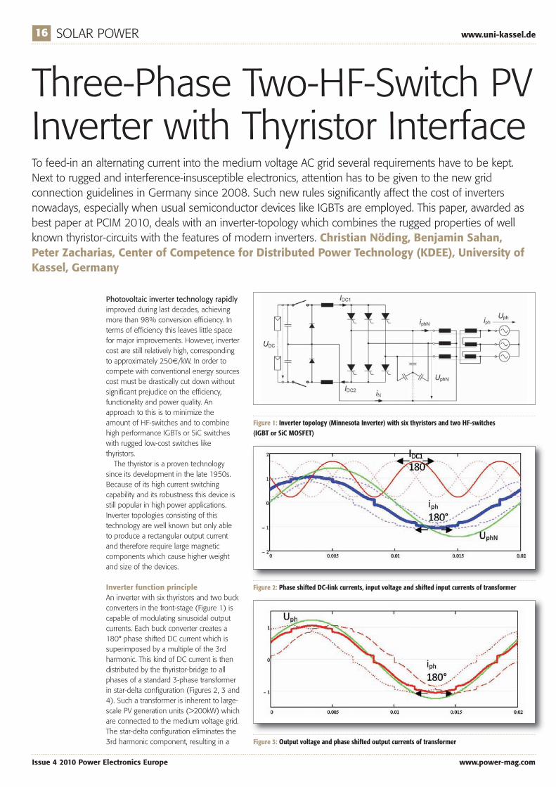
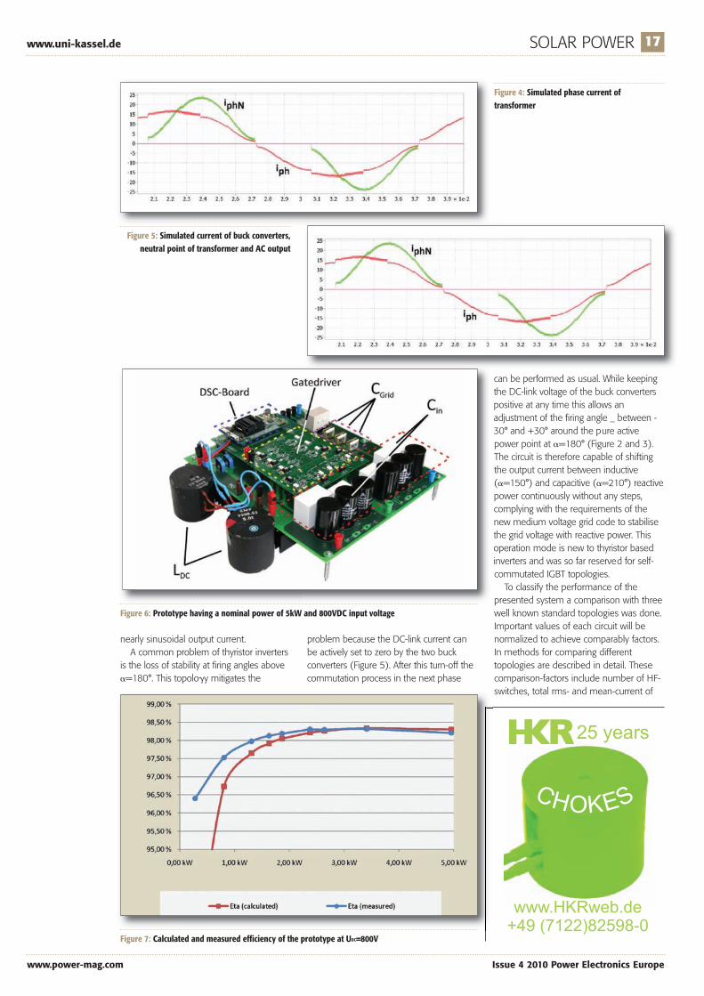
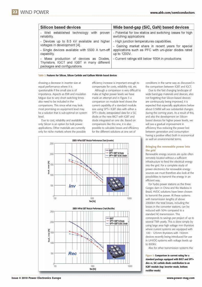
Inverter function principleAn inverter with six thyristors and two buckconverters in the front-stage (Figure 1) iscapable of modulating sinusoidal outputcurrents. Each buck converter creates a180° phase shifted DC current which issuperimposed by a multiple of the 3rdharmonic. This kind of DC current is thendistributed by the thyristor-bridge to allphases of a standard 3-phase transformerin star-delta configuration (Figures 2, 3 and4). Such a transformer is inherent to large-scale PV generation units (>200kW) whichare connected to the medium voltage grid.The star-delta configuration eliminates the3rd harmonic component, resulting in a
Figure 1: Inverter topology (Minnesota Inverter) with six thyristors and two HF-switches (IGBT or SiC MOSFET)
Figure 2: Phase shifted DC-link currents, input voltage and shifted input currents of transformer
Figure 3: Output voltage and phase shifted output currents of transformer
BPA_Kassel Feature_Layout 1 03/06/2010 14:07 Page 16
www.uni-kassel.de SOLAR POWER 17
www.power-mag.com Issue 4 2010 Power Electronics Europe
problem because the DC-link current canbe actively set to zero by the two buckconverters (Figure 5). After this turn-off thecommutation process in the next phase
can be performed as usual. While keepingthe DC-link voltage of the buck converterspositive at any time this allows anadjustment of the firing angle _ between -30° and +30° around the pure activepower point at �=180° (Figure 2 and 3).The circuit is therefore capable of shiftingthe output current between inductive(�=150°) and capacitive (�=210°) reactivepower continuously without any steps,complying with the requirements of thenew medium voltage grid code to stabilisethe grid voltage with reactive power. Thisoperation mode is new to thyristor basedinverters and was so far reserved for self-commutated IGBT topologies.To classify the performance of the
presented system a comparison with threewell known standard topologies was done.Important values of each circuit will benormalized to achieve comparably factors.In methods for comparing differenttopologies are described in detail. Thesecomparison-factors include number of HF-switches, total rms- and mean-current of
nearly sinusoidal output current.A common problem of thyristor inverters
is the loss of stability at firing angles above�=180°. This topolo�y mitigates the
Figure 4: Simulated phase current oftransformer
Figure 5: Simulated current of buck converters,neutral point of transformer and AC output
Figure 6: Prototype having a nominal power of 5kW and 800VDC input voltage
Figure 7: Calculated and measured efficiency of the prototype at UDC=800V
BPA_Kassel Feature_Layout 1 03/06/2010 14:07 Page 17

18 SOLAR POWER www.uni-kassel.de
Issue 4 2010 Power Electronics Europe www.power-mag.com
the semiconductors, total switching-lossvalues and number and volume ofrequired inductors. All factors arenormalized to the values of the well known2-level inverter.
To estimate the pros and cons of eachcircuit, factors for four topologies werecalculated with simulation results(Simulink/PLECS) and listed in Table 1. Allfactors are normalized values in referenceto the 2-level inverter topology at amodulation index of 1 and cos�=1.
Experimental resultsA laboratory prototype (Figure 6) has beenbuilt having a nominal power of 5kW,800VDC input voltage and switchingfrequency of 16kHz to verify the feasibilityof the approach.
To estimate the potential of thistopology the calculated efficiency wascompared to the measured one feedingan ohmic load (Figure 7). A peak efficiencyof 98.4% could be achieved. Due to apessimistic switching loss assumption thecalculated efficiency within low powerregion is below the measured one.
ConclusionsAn inverter topology for photovoltaicsystems connected to the medium voltagegrid using inexpensive thyristors and highperformance IGBTs or SiC switches hasbeen presented. A three-phase sinusoidalcurrent can be generated while complyingwith the reactive power specifications ofthe new medium voltage grid code.Reactive power is an important part ofmodern inverters for grid stability andcompensation features. The majoradvantages of the circuit are the highperformance/cost ratio and the robustnessof the semiconductors. Using factors forcomparing different types of topologies acomparison between common inverterswas made to show the benefits of thepresented system. The feasibility of thistopology was proved by experimentalresults presented in this paper, showing itscorrect operation even with firing anglesabove �=180°. With only two IGBTswitches a peak efficiency of 98.4% couldbe reached with this laboratory setup.Further research of this concept will befocused on behavior of the circuit onsingle- and multi-phase errors defined inthe new grid code.
LiteratureChristian Nöding: “Evaluation of a
Three-Phase Two-HF-Switch PV Inverterwith Thyristor-Interface and ActivePower Factor Control”, PEE SponsoredBest Paper Award in Session “Invertersfor Renewable Energy and UPS”, PCIMEurope 2010, May 6, Room London
Low-ohmic precision resistors VMx
Features: 3 watt power loss (size 2512) max. 25 A constant current Tcr < 20 ppm/K Rthi < 20 K/W
This is unrivalled quality
Telephone: +49 (27 71) 9 [email protected]
www.isabellenhuette.de
Innovation from tradition
The winning pitch
Table 1: Simulationresults
(Simulink/PLECS) forfour topologies
normalized to the 2-level inverter
BPA_Kassel Feature_Layout 1 03/06/2010 14:07 Page 18

Complete thermal solutions for automated dispensing.Gap Filler 1500 is just one of our many robust thermal solutions thatboost your process performance. Confidently tackle your high volumedispensing needs by capitalizing on our expertise. Bergquist can guide youto the best thermal solution from gap fillers to dispensing. Our thermal/ ) ! � # � " % . � * + / . � * * / . " � * . � ! ) + � % . * + * � " ) ! ,� . � ! � / ! * " % . ) # , � . � ! ! + �
Learn more with a FREE Sample Kit.Take a closer look by getting your FREE Gap FillerSample Kit today.Simply visit our website or call usdirectly to qualify.
Liquid Gap Filler1500(Two-Part) Dispenses Where You Want It,Without “Stringing”, Offers Superior Thermal Conductivity.
Gap Filler1500 forms-in-place, offers faster throughputwith reduced pressure – putting less stress on equipment.Gap Filler1500 is an advanced thermal material specifically designed tosupport optimized dispensing control and exhibits an excellent thermalconductivity of 1.8 W/mK. This material features superior slump resist-ance and high shear thinning characteristics for maximum dispensingcontrol. Its smooth dispensing results inprecise material placement, in half thetime as compared to one-part materials.As a mixed system, it cures at roomtemperature and can be acceleratedwith the addition of heat. It is designedto fill unique and intricate gaps andvoids without stress.
FREE Promo Pocket withDispensed Sample and Data Insert.Call +31 (0) 35 5380684 or visit www.bergquistcompany.com/noslump
B E R G Q U I S T H I G H - P E R F O R M A N C E L I Q U I D G A P F I L L E R S
NowThere’s A LiquidGap FillerThatWon’t
Miss Any Curves.
Gap Filler 1500 has natural tack and cleanly flows into positionfor final assembly without leaving thermal material behind.
Thermal Products • Membrane Switches • Touch Screens • Electronic Components
European Headquarters - The Netherlands. Tel: EU +31 (0) 35 5380684 . D +49-4101-803-230 . UK +44-1908-263663
19_PEE_0410_19_PEE_0410 03/06/2010 14:10 Page 1

Power SemiconductorTechnologies for RenewableEnergy Sources
20 WIND POWER www.abb.com/semiconductors
Issue 4 2010 Power Electronics Europe www.power-mag.com
High power semiconductors are key components for controlling the generation and connection to thenetwork of renewable energy sources such as wind-turbines and photovoltaic cells. For a highest efficiencyof the energy source, it is therefore essential to select the right device for the given conditions. This articlelooks at the performance features for the available high power semiconductors of choice and also takes alook at future device technologies and their expected impact on efficiency. Björn Backlund and MunafRahimo, ABB Switzerland Ltd, Semiconductors, Lenzburg, Switzerland
Renewable energy sources as wind-turbines and photovoltaic cells havereached power levels of several MWswhich have resulted in the need for highpower semiconductor devices foroptimized generation and networkconnection. The state-of-the-art devices ofchoice for these power levels are theIGBTs and IGCTs. Due to the power qualityrequirements, the earlier used solutionswith thyristors in the wind turbines arerarely seen today. During the last 15 years,high power semiconductors have gonethrough a remarkable development.Several new generations of IGBT-dies havelead to a reduction in VCEsat of almost 40 %since the early 1990s, and still a potentialfor further improvement is available. TheBipolar devices have also seen largeimprovements where the introduction ofthe IGCT have had a large impact on theMV-Drive design and higher ratings forthem have recently been introduced or arein development. The thyristors have alsonot been standing still but have moved
from 6500 V, 2600 A to 8500 V, 4000 Adevices based on 150mm silicon now inproduction.The power semiconductors are used for
two main tasks in the chain of renewableenergy sources such as conversion of thepower in the plant, as in wind-turbines,and transmission of the power to the grid.The best solution to determine whatsemiconductors to use for these tasks is tomove top-down by following the pathsystem requirements defining equipmentrequirements which in turn are definingthe power semiconductor requirements.Through this chain the requirements onthe devices are determined regardingitems as required voltage and currentratings, needed degree of controllability,and operating frequency.
Power semiconductors for invertersThe possibilities to achieve the aboverequirements will be looked at with focusat power ratings above 0.5 MW. Forinverter applications, the IGBTs and IGCTs
represent the two main candidates due tothe main features listed in Table 1.As can be seen, both devices have a
distinct set of features making the questionwhich one is the best technology obsolete.What it comes down to is to select thedevice based on application requirementsand own capability to utilize the device toits best. Certain comparisons are thoughhelpful to see what is possible to achievewith the two technologies. One example isthe possible out-put power for a 2-levelinverter as function of the switchingfrequency at a given set of conditions asseen in Figures 1 and 2. Othercomparisons can though have beenselected to promote a certain technologyover another and should not be used tofind out which solution is the best for thegiven task.In practice the choice of components
will be governed by considerations asstandardization by the use of basic buildingblocks for various applications andrequests from customers to use a certain
Table 1: Features for IGCT and IGBT
ABB Feature_Layout 1 03/06/2010 14:23 Page 20

www.abb.com/semiconductors WIND POWER 21
www.power-mag.com Issue 4 2010 Power Electronics Europe
comparisons is that SiC and GaN arelimited in voltage, current and componenttypes which means that usefulcomparisons for many systems inrenewable energy are not really possiblesince there are for instance nocomparative GaN and SiC components to
the Silicon-based IGCTs used in 5MW windturbines with full power conversion. Thisoften leads to comparisons for specialcomponents in special applications wherea 1 to 1 comparison is possible thus toooften underestimating the potential ofenergy savings made possible by Silicon or
solution. The fast development of thedevices makes it though necessary to lookcritically at the used solution from time totime to see if it still is the best possibility tofulfill the requirements or if new designswith new devices can improve theequipment performance.
Since the operating conditionsdetermine the preferred semiconductortechnology it is also not possible to givegeneral rules about which component hasthe highest efficiency. This has to bedetermined case by case also consideringthat the different features of the devicetechnologies can have an impact on thecomplete efficiency for the system. It canthough be projected that the efficiency isnot static but will improve with time asnew improved power semiconductors arecontinuously being introduced on themarket.
Wide band-gap materialsAnother interesting item is thedevelopment of new wide band-gapsemiconductor materials in addition to thedominating silicon starting material. Thesalient features of Silicon compared withthe most developed candidates for newsemiconductor materials are listed in Table2. One important aspect of the high powersemiconductor development is its impacton efficiency and energy saving, or in otherwords how “green” it is. Renewable energysources are today almost exclusivelyequipped with power electronics andtherefore it makes a difference what powersemiconductor are used also due to thelarge impact of secondary effects ascooling capacity.
One major issue for efficiency
Figure 1: Comparison in current rating for astandard package equipped with SPT dies
Figure 2: Comparison in current rating forstandard IGCTs
WHEN WE IMPROVE OUR PHOTOCOUPLERSWE THINK BIG – AND SMALL.As a leading manufacturer of photocouplers, Toshiba’s product range continues to pioneerinnovation. Like lower power consumption and higher switching speed. Yet it’s all in newsmaller packages. Our latest SDIP package is 50% smaller than previous devices andis ideal for circuits that require the reinforced isolation demanded for international safetycertification.
Whether your application is for industrial or domestic appliances, drives or factoryautomation interfaces, when you want less, Toshiba gives you more.
Visit us today at www.toshiba-components.com/photocouplers
ABB Feature_Layout 1 03/06/2010 14:23 Page 21
22 WIND POWER www.abb.com/semiconductors
Issue 4 2010 Power Electronics Europe www.power-mag.com
showing a decrease in inverter size atequal performance where it isquestionable if the small size is ofimportance. Aspects as EMI and insulationfatigue due to very short switching timesalso need to be included in thecomparisons. This since what may lookmost promising on equipment level maybe a solution that is sub-optimal on systemlevel.Due to cost, reliability and availability
only Silicon is an option for bulk powerapplications. Other materials are currentlyonly for niche markets where the possible
efficiency increase is important enough tocompensate for costs, reliability risk, etc.Although a comparison is very difficult to
make at higher power levels we havemade an attempt and in Figure 3 acomparison on module level shows thecurrent capability of a standard modulesize using SPT+ IGBT dies with either aSPT+-diode, extrapolated data for a SiCdiode or the new BIGT with IGBT anddiode integrated on one die. Based oncomparisons like this one, it is alsopossible to calculate losses and efficiencyfor the different solutions at one set of
Table 2: Features for Silicon, Silicon Carbide and Gallium Nitride based devices
conditions in the same way as discussed inthe comparison between IGBT and IGCT. Due to the fast changing landscape of
wide band-gap materials and devices, alsonot forgetting that Silicon-based devicesare continuously being improved, it isexpected that especially applications belowabout 0.5MW will see substantial changesduring the coming years. As a result of this,and also the development on Silicon-based devices for higher power levels, wewill see a gradual improvement inefficiency thus reducing the power lostbetween generation and consumptionhaving a positive effect both in economicalas well an environmental terms.
Bringing the renewable power intothe grid Renewable energy sources are quite oftenremotely located without a sufficientinfrastructure to feed the electrical energyinto the grid. For a complete study ofpower electronics for renewable energysources we must therefore also look at thepossibilities to transmit the energy in anefficient way. For hydro power stations as the three
Gorges dam in China and Rio Madeira inBrazil, HVDC solutions have been chosento transmit the power. At these systemswith transmission lengths of above2000km the total losses, including thelosses in the converter stations, can bereduced with 50% compared to astandard AC-transmission. Thiscorresponds to savings per project of up toseveral TWh yearly. This is done simply byusing large area high voltage mm thyristorswhere current systems are equipped with100 - 125mm thyristors with 150mmdevices recently being introduced for usein UHVDC-systems with voltage levels upto 800kV.Also for other transmission systems the
Figure 3: Comparison in current rating for astandard package equipped with BIGT and SPT+dies vs. SiC carbide diode contribution to anIGBT module (top: inverter mode, bottom:rectifier mode)
ABB Feature_Layout 1 03/06/2010 14:23 Page 22

www.abb.com/semiconductors WIND POWER 23
www.power-mag.com Issue 4 2010 Power Electronics Europe
losses and costs can be largely reduced bythe use of HVDC transmission techniques,which is especially apparent for off-shorewind parks where power in the range of300 - 500MW will be transmitted throughthe sea to sub-stations on land. The HVDCLightTM system (Figure 4) is based on IGBTtechnology with a special design thatensures that the module remains shortedin case of a failure enabling a continuationof operation if redundancy is built into thesystem. Starting at the tender power levelof 3MW back in 1997 these systems hasgradually grown larger and it is a merequestion of time until voltage sourceconverter based HVDC-systems with theuse of the latest power semiconductortechnologies will brake the GW-barrier.
Small scale renewable energy with alarge number of units spread over a largearea also create issues for the grid stabilitywhich can be solved with differentmeasures normally referred to as smartgrids. Although power electronics will playan important part in these systems, weleave them out of the discussion heresince they are not directly connected toefficiency of renewable energy sources.
ConclusionsRenewable energy sources as wind
turbines and photo-voltaic cells havegrown rapidly in size and power in recentyears. The requirements on them fornetwork compatibility have also increasedsince their impact on the grid is far fromnegligible. Due to a steady developmenton the high power semiconductor side,devices are available to meet therequirements on controllability andefficiency and new devices and devicematerials are on the way enabling furtherimprovements. To utilize the possibilitiesto their optimum the device choiceshould only be made when therequirements and operating conditions forthe high power semiconductors areknown. To use a device just because it ispopular among other users may notmean that it is the best choice for everycase since the best device is determinedby the particular circumstances for theactual project.
LiteratureBjörn Backlund: “Comparison of High
Power Semiconductor Technologies forRenewable Energy Sources”, PEESpecial Session “Power Electronics forEfficient Inverters in Renewable EnergyApplications”, PCIM Europe 2010, May4, Room Paris
Figure 4: Sea cable for an HVDC LightTM system islaid out for connection of an off-shore windpark to the main land grid
ABB Feature_Layout 1 03/06/2010 14:28 Page 23

New Design Proposals forHigh-Power Renewable Energy Applications
24 WIND & SOLAR POWER www.semikron.com
Issue 4 2010 Power Electronics Europe www.power-mag.com
Renewable energy applications are a great challenge for Power Electronics, with efficiency and reliabilitybeing the prevailing requirements. Today, 1700V low-voltage Silicon is vastly superior. For input/outputpowers of several MW, dozens of modules with dozens of chips need to be connected in parallel. The bestsolution is paralleling inverters / power blocks, but such solutions require additional low-voltagetransmission from the source to the medium-voltage (MV) transformer. An alternative solution is a MVsource and transmission connected to MV grid-side inverter based on low-voltage Silicon - power blocks -connected in series. In addition, interleaved PWM reduces the size of the sinusoidal filter and the switchingfrequency, as well as the total losses. Dejan Schreiber, Senior Application Manager, Semikron,Nuremberg, Germany
Existing new high-power renewableenergy sources are wind turbines (WT)and photovoltaic (PV) applications. Theaverage power of new WTs is over 2MW,but up to 5MW are also in use. As for PV,over the last few years, the trend has beento use individual units of up to 0.5MW,with an increasing tendency towards1MW+ per unit. Large PV systems of10MW are the most common and up to60MW are in operation. Both areconnected to the grid through line-sideinverters, and both supply the grid withlow THD (total harmonic distortion)sinusoidal currents via sinusoidal filters.WTs have generator-side converters with
boost features, rectifying the variablegenerator voltage to constant DC voltagerequired for optimal operation of the grid-side converter. Similarly, PV panels supplyconverters with voltage proportional tosunlight intensity, ambient temperature,load current, and power. The result is avariable input voltage in the range of morethan 1:2. Typically high-power PV grid-sideinverters do not use additional front-endconverters.Power converting efficiency is the No.1
priority. Today, power electronics (PE) usesindustrial Silicon-based components of1200V and 1700V for WTs and 1200V forPV applications (600V for low-powersingle-phase supply). The system efficiencycan be improved with reduced converter
losses by using the right Silicon and newbetter semiconductors technologies. Thisarticle shall not, however, dwell on this forthe simple reason that IGBT’s will remainthe work horse of power electronics for thenext 5 to 10 years, with no notablechanges to speak of.WT designs based on a doubly fed
induction generator (DFIG) are going outof fashion. In fact, WT companies thatemploy DFIG technology are now basingtheir new developments on the full-sizeprinciple, the traditional 4-quadrant drive.WT converter efficiency today, for a full-sizeconstruction with two serial powerelectronics converters placed in onecasing, and measured from the generatoroutput through generator dv/dt filter,generator-side converter, DC link, grid-sideinverter and output sinusoidal filter, is in
the range of 96-97%. Power convertersizing is driven by price and high reliabilityrequirements. Reliability is a very important factor. A
wind turbine must not stop working, mustnot stop turning! First-rate components aretherefore an absolute must. What is alsoimportant, however, is to have a turbinedesign which enables continued operationshould an individual component fail. Thelarge inverter powers in the range ofseveral MVA require considerablequantities of semiconductor chips inparallel, and this is accomplished byparalleling modules.
Solutions for parallel operation ofIGBT modules1) One inverter phase unit is used for theentire power with one driver for many
Figure 1: Turbine construction with threegenerator windings and independent
drive trains
Semikron Feature_Layout 1 03/06/2010 14:31 Page 24

www.semikron.com WIND & SOLAR POWER 25
www.power-mag.com Issue 4 2010 Power Electronics Europe
modules of 1700V have to be used inparallel for one three-phase inverter of 1MW;the maximum available power of a singlethree-phase inverter today is 1.5MW.Therefore, solutions with several generatorwindings facilitate parallelization ofindependent drive trains. At the same time,the reliability of this design is higher than thatof designs with one high-power converterwith the same number of modulesconnected in parallel (see Figure 1).
WT generatorsGenerator requirements such as minimumsize, ripple torque, and short circuit torque,especially for low-speed, direct-drivegenerators, result in generator solutionswith a number of phases, such as 2 or 3 xthree-phase windings, or 6 x three-phasewindings. Generators with poly-phasesystems of 5 or 7 or more phases are notused, because of standard industrial three-phase inverters and controllers. Forgenerator sizes in the range of several MW,the traditional method is a medium-voltageoutput. MV inputs & outputs, however,require the use of MV PE components.State-of-the-art MV converters used on thegrid side, with switching frequencies ofseveral kHz, have a much lower efficiencyand are far more expensive per kW.Additional requirements for renewable
energy sources are: active power control,
reactive power control, low-voltage ride-through capability, as well as a requirementmentioned less often, namely operationunder unsymmetrical grid voltages.Reactive power control for renewableenergy sources, initially used in WTs, andmore recently for PV applications, calls forhigher DC link voltage input to the line-sideinverter.Power flow in the PWM converter is
controlled by adjusting the phase shiftangle � between the source voltage U1and the respective converter reflectedinput voltage Vs1. When U1 leads Vs1 the real power
flows from the AC source into theconverter. Conversely, if U1 lags, Vs1power flows from the converter’s DC sideinto the AC source. The real powertransferred is given by equation 1:
The AC power factor is adjusted bycontrolling the amplitude of Vs1. The perphase equivalent circuit and phasediagrams of the leading, lagging and unitypower factor operation is shown in Fig.2.The phasor diagram shows that to achievea unity power factor, Vs1 has to beaccording to equation 2
Proposal for series connection of highpower WT inverter cells WT designs with full size converters basedon separate generator windings have manyadvantages, but also one large drawback.Many cables are required between thegenerator and the converter - 3 x three-phase winding set. All of these convertersare therefore situated near the generator,in the nacelle. For high powers at lowvoltages, the generator currents are >>1500A. An attractive solution is the MVsynchronous generator and only a dioderectifier. However, in this case, the DC
IGBT modules in parallel. Each IGBTmodule has its own gate resistors andsymmetrical DC & AC connections. Onesuccessful example is SEMIKUBE IGBTpower STACK, for use in PV applications.
2) Paralleling of several inverter-phaseunits, each with own driver operating inparallel. Due to different driver delaytimes, small AC output chokes are alsorequired (paralleling of SKiiP IPM powerstack).
3) Paralleling of three-phase units with aDC link and several modules in parallel,driven by its own drivers. For higherpower, several three-phase inverters areconnected in parallel. Due to differentdriver delay times, AC output chokesare still needed. One PWM signal andone DC link are in use.
4) Parallel operation of three-phaseinverters with one PWM controller andadditional control of load currentsharing of parallelized inverters(sophisticated PWM control).
5) Master-slave drivers with short delaytimes, driving the several modulesconnected in parallel. There is no needfor any additional inductances, and inthe event of damage to asemiconductor chip, only one modulewill be damaged.
6) Parallel inverter operation with galvanicisolation on input or output side - is theoperation in parallel of standard,independent basic units with differentPWM and separate controllers. In some WT designs, the generator and
the entire drive train, as well as the MVtransformer, are placed in the nacelle. Inthese cases, the total weight of the nacelleis very high, but it’s the only way to makethe transmission losses between the LVgenerator and the MV grid bearable. Inother designs, the WT drive train is locatedat the bottom, at the base of the tower.Power transmission over that distance ofabout 100m is low-voltage, with highpower losses and cost.Standard industrial Silicon-based IGBT
Figure 2: Per phaseequivalent circuit of
the line-side inverterand phasor diagrams
for unity, leading,and lagging power
factor operation
Figure 3: MV generator with MV grid-side inverter with several cells connected in series
Semikron Feature_Layout 1 03/06/2010 14:31 Page 25
26 WIND & SOLAR POWER www.semikron.com
Issue 4 2010 Power Electronics Europe www.power-mag.com
voltage variations are large (1:2) andrequire MV Silicon devices. As the WT issupposed to produce power even atminimal rotation speed and a minimal DCvoltage, for instance for 1000VDC, theoutput voltage at the MV transformer isrelatively low, i.e. 660V. At the same time,DC voltage may reach more than 2kV.A logical solution to the MV grid-side
inverter is a string of series connectedinverters, which can divide the variablerectified generator voltage. These grid-sideinverter cells are connected to the primarywindings of the MV line transformer, andindependently maintain their DC linkvoltages. For lower generator voltages,some of the cells must be bypassed, sothat the equivalent total voltage of the cellsis lower and corresponds to the generatorvoltage. The WT torque requirement is thesame as the generator currentrequirement; it is therefore compared withthe real, actual value of the DC current. Ifthe torque demand is higher than theactual current DC value, the sum of bypasstimes should be larger, more cells arebypassed and the equivalent counter-EMFwill be lower, thus increasing DC current. Each of the grid-side inverters used
controls and maintains constant input DCvoltage, for instance 1000V, and isconnected to the primary winding of thetransformer. If the DC voltage is higherthan a set value, the discharge currents willbe larger. The grid-side inverters can besingle- or three-phase units. Single-phaseunits have only one transformer winding.The rectified generator MV, for instance adozen kV, supplies this string of invertercells. Some cells have input bypassswitches which allow for DC link control,and some cells can have no input bypass.They are always connected in series andthe sum of their voltages corresponds tothe minimum generator voltage.Described below is a power conversion
scheme for MW-class wind turbinesconsisting of a medium-voltagesynchronous generator, a diode rectifier inthe nacelle, and an MV DC-efficient powertransmission down to the MV line-sideinverter and the high-voltage gridtransformer (see Figure 3). Several cellsthat share the variable output generatorvoltage are also used. Each cell has a grid-side inverter, three-phase or single-phase,separate transformer windings and DC linkcapacitors. The input power - the currentfrom the MV generator - charges the DClink, and the converter discharges it. This iswhy the DC link voltage remains constant,because the grid-tie inverter controls theDC discharge current to the grid. The cellinput features one half-bridge configuration,for instance a conventional booster; thisoperates, however, as a bypass switch only.
If the generator voltage is lower than thesum of the series connected cells, thecurrent from the generator will decline.More cells therefore have to be bypassed,reducing the number of series cells andincreasing the generator current.
PV applicationsPV applications usually have only one PEline-side grid-tie inverter (GTI). GTI ACoutput voltage is proportional to theminimum DC input voltage - the start-upPV voltage proportional to the minimumsunlight. If the chosen AC output voltage islower, the currents for the rated power willbe higher; at the same time, however, thestart-up voltage will be lower. The ACoutput voltage is therefore a compromise:some products use 3 x 270V, while othersuse 3 x 328 V. The higher AC output voltage design
neglects the minimum energy that couldbe used if the PV voltage / output ACvoltage is lower. In a PV application, GTIoperate at approximately 1/2 of the ratedoutput voltage only; 1200V silicon isdeveloped for input/output voltage of upto 480VAC, and PV applications today usejust 270V...330V. The efficiency of suchoperation is lower, because it is stronglyrelated to the modulation factor m,VAC/VDC ratio. For 400VAC/650VDC or480VAC/800VDC, the efficiency is verysimilar and higher than the ratio used in PV
applications of 270VAC (500...900VDC)(see Figure 4). Described below is a power conversion
scheme (Figure 5) for MW-class PVconsisting of solar panels, an active front-end with symmetrical voltage boostersnext to the solar panels, a DC transmissionline to the inverter station, industrial grid-side converter, sinusoidal filter, andstandard line voltage / MV transformer.Inverter input voltage is optimized to the
AC transformer input voltage, and themodulation factor m is close to 1according to equation 3:
Sample application from the USA: Circuitfrom Figure 5 PV voltage is in the range of200V-600V; booster output voltage /transmission voltage is 800VDC; output:3x480V, a standard transformer is in use.600V Silicon is used for the front end, and1200V for the inverter. For a PV voltage of400V, for example, the DC transmissionlosses are four times lower, while thetransmission voltage is 800V. Therequirement is to have a relatively lowripple current from PV panels, and this canbe achieved with higher inductancebetween the PV panels and the front-endunit, but also with increased switchingfrequency. The inductance of the
Figure 4: GTI (grid-tied inverter) efficiency at various power; switching frequency 5kHz
Figure 5: Voltage booster and GTI
Semikron Feature_Layout 1 03/06/2010 14:31 Page 26
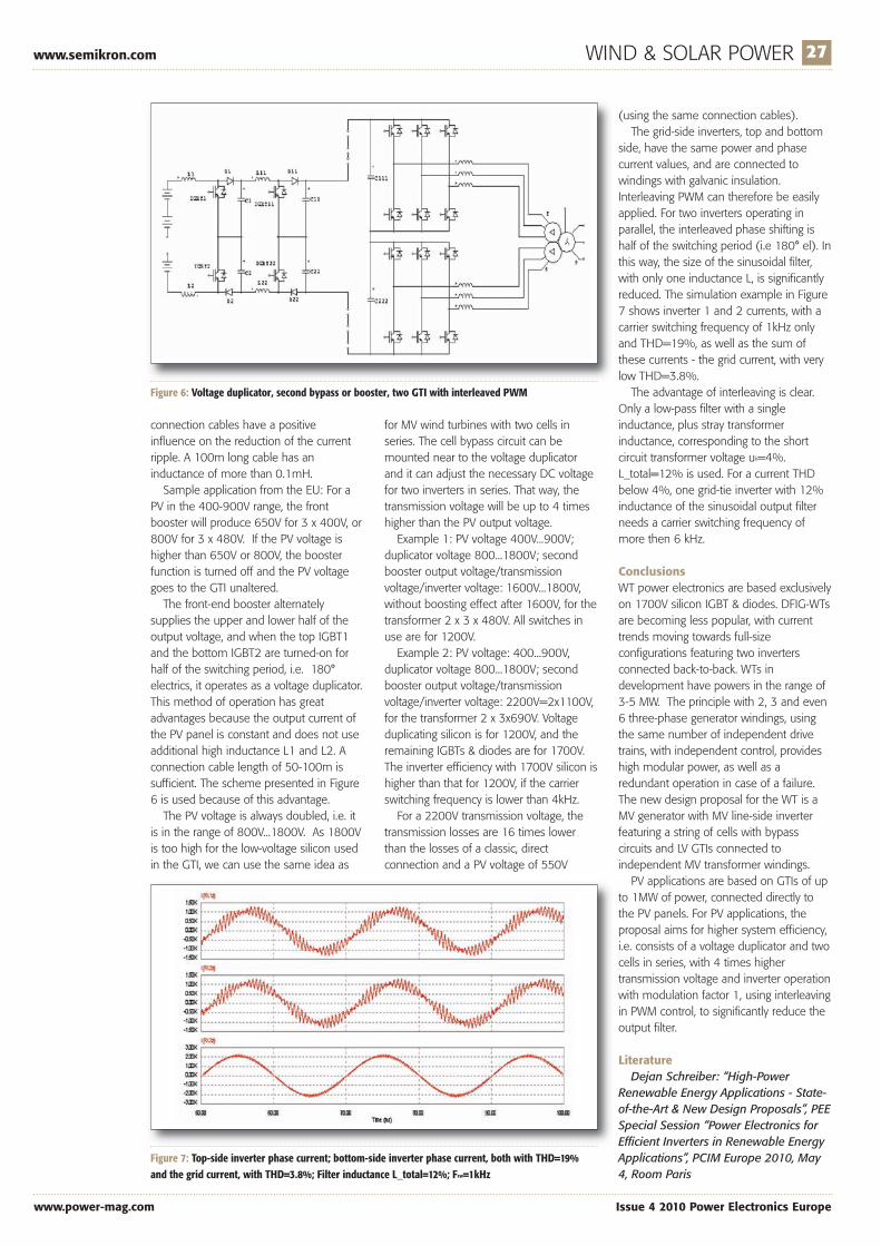
www.semikron.com WIND & SOLAR POWER 27
www.power-mag.com Issue 4 2010 Power Electronics Europe
connection cables have a positiveinfluence on the reduction of the currentripple. A 100m long cable has aninductance of more than 0.1mH. Sample application from the EU: For a
PV in the 400-900V range, the frontbooster will produce 650V for 3 x 400V, or800V for 3 x 480V. If the PV voltage ishigher than 650V or 800V, the boosterfunction is turned off and the PV voltagegoes to the GTI unaltered. The front-end booster alternately
supplies the upper and lower half of theoutput voltage, and when the top IGBT1and the bottom IGBT2 are turned-on forhalf of the switching period, i.e. 180°electrics, it operates as a voltage duplicator.This method of operation has greatadvantages because the output current ofthe PV panel is constant and does not useadditional high inductance L1 and L2. Aconnection cable length of 50-100m issufficient. The scheme presented in Figure6 is used because of this advantage.The PV voltage is always doubled, i.e. it
is in the range of 800V...1800V. As 1800Vis too high for the low-voltage silicon usedin the GTI, we can use the same idea as
for MV wind turbines with two cells inseries. The cell bypass circuit can bemounted near to the voltage duplicatorand it can adjust the necessary DC voltagefor two inverters in series. That way, thetransmission voltage will be up to 4 timeshigher than the PV output voltage.Example 1: PV voltage 400V...900V;
duplicator voltage 800...1800V; secondbooster output voltage/transmissionvoltage/inverter voltage: 1600V...1800V,without boosting effect after 1600V, for thetransformer 2 x 3 x 480V. All switches inuse are for 1200V.Example 2: PV voltage: 400...900V,
duplicator voltage 800...1800V; secondbooster output voltage/transmissionvoltage/inverter voltage: 2200V=2x1100V,for the transformer 2 x 3x690V. Voltageduplicating silicon is for 1200V, and theremaining IGBTs & diodes are for 1700V.The inverter efficiency with 1700V silicon ishigher than that for 1200V, if the carrierswitching frequency is lower than 4kHz. For a 2200V transmission voltage, the
transmission losses are 16 times lowerthan the losses of a classic, directconnection and a PV voltage of 550V
(using the same connection cables).The grid-side inverters, top and bottom
side, have the same power and phasecurrent values, and are connected towindings with galvanic insulation.Interleaving PWM can therefore be easilyapplied. For two inverters operating inparallel, the interleaved phase shifting ishalf of the switching period (i.e 180° el). Inthis way, the size of the sinusoidal filter,with only one inductance L, is significantlyreduced. The simulation example in Figure7 shows inverter 1 and 2 currents, with acarrier switching frequency of 1kHz onlyand THD=19%, as well as the sum ofthese currents - the grid current, with verylow THD=3.8%. The advantage of interleaving is clear.
Only a low-pass filter with a singleinductance, plus stray transformerinductance, corresponding to the shortcircuit transformer voltage uk=4%.L_total=12% is used. For a current THDbelow 4%, one grid-tie inverter with 12%inductance of the sinusoidal output filterneeds a carrier switching frequency ofmore then 6 kHz.
ConclusionsWT power electronics are based exclusivelyon 1700V silicon IGBT & diodes. DFIG-WTsare becoming less popular, with currenttrends moving towards full-sizeconfigurations featuring two invertersconnected back-to-back. WTs indevelopment have powers in the range of3-5 MW. The principle with 2, 3 and even6 three-phase generator windings, usingthe same number of independent drivetrains, with independent control, provideshigh modular power, as well as aredundant operation in case of a failure.The new design proposal for the WT is aMV generator with MV line-side inverterfeaturing a string of cells with bypasscircuits and LV GTIs connected toindependent MV transformer windings. PV applications are based on GTIs of up
to 1MW of power, connected directly tothe PV panels. For PV applications, theproposal aims for higher system efficiency,i.e. consists of a voltage duplicator and twocells in series, with 4 times highertransmission voltage and inverter operationwith modulation factor 1, using interleavingin PWM control, to significantly reduce theoutput filter.
LiteratureDejan Schreiber: “High-Power
Renewable Energy Applications - State-of-the-Art & New Design Proposals”, PEESpecial Session “Power Electronics forEfficient Inverters in Renewable EnergyApplications”, PCIM Europe 2010, May4, Room Paris
Figure 6: Voltage duplicator, second bypass or booster, two GTI with interleaved PWM
Figure 7: Top-side inverter phase current; bottom-side inverter phase current, both with THD=19%and the grid current, with THD=3.8%; Filter inductance L_total=12%; Fsw=1kHz
Semikron Feature_Layout 1 03/06/2010 14:31 Page 27

GaN Power Devices for Micro Inverters
28 SOLAR POWER www.irf.com
Issue 4 2010 Power Electronics Europe www.power-mag.com
GaN power products are set to have a direct impact on future efficient PV solar inverter/converters. By reducing losses in each stage of the power conversion, GaN based devices will help in increasing totalenergy harvesting. The integration with driver ICs and other components will drive the size reduction andhigh volume commerzialisation. Alberto Guerra and Jason Zhang, International Rectifier, El Segundo, USA
The PV industry has shown varioustrends for increasing overall conversionefficiency as well as maximizing theharvesting of solar energy. The specifictrend toward an intelligent PV panelrequires high efficiency, high reliability andlow cost. “In-situ” conversion and “in-situ”pre-regulation with micro-inverters/converters require highly efficientDC/DC stage.
All topologies based on SiliconMOSFETs have intrinsically limitedimprovement capabilities. Based on state-of-the-art active components and passivecomponents, constrained integrationopportunities pose a limit to thetechnology evolution. Gallium Nitride(GaN) based switches, have a better figureof merit (FOM) than other powercomponents based on Si (Silicon) or SiC(Silicon Carbide) material (Figure 1).
The potential improvement exploitablefrom the GaN technology is large, basedon the material limits. The primaryconversion stage of micro-inverters andmicro-converters can be designed aroundwell known topologies (Fly-Back, FullBridge or Buck-Boost). To improve overall
conversion efficiency, all these topologiesrequire the power MOSFETs with thelowest possible specific RON x QG FOM. GaNbased MOSFETs show great potential inFOM improvement over the coming years(Figure 2).
Practical impact of GaN technology inPV applicationsGaN technology is characterized by anintrinsic lateral structure, which simplifies
packaging by virtually eliminating parasiticelements of wire-bonding stray inductanceand parasitic resistance. Moreover, itenables possible integration of multipleswitches and driver IC function withprotection and monitoring elements withincommon packaging or monolithicsolutions. The integration capabilities ofGaN technology can simplify and reducethe cost of design and construction ofpower circuits for solar inverterapplications.
The expansion of small and mid-sizesolar installation is opening new alternativevenues diverging from the traditionalcentral inverter architecture. Adopting adistributed inverter architecture, micro-inverters or dc-dc solutions, certainadvantages over the traditional centralizedarchitecture, are made possible and,among them, the ability to implementmaximum power point tracking (MPPT) atthe panel level. In addition, thesedistributed solutions are required toprocess only the power generated by asingle PV panel, typically in the range of200W; this specific characteristic isopening the possibility for higher degree ofpower semiconductor integration that inFigure 1: Comparison of Specific RON for Si, SiC and GaN.
Figure 2: Possible 150V GaN FOM projection vs.Si MOSFET
IRR Feature_Layout 1 03/06/2010 14:36 Page 28

www.irf.com SOLAR POWER 29
www.power-mag.com Issue 4 2010 Power Electronics Europe
inverter (DC/AC) used for the comparisonand GaN switch evaluation ismanufactured by Enphase Energy, whilethe DC/DC Power Optimizer utilized forthe buck-boost topology evaluation, ismanufactured by SolarEdge. Both systems,intended for “in-situ” single PV panelconnection, have the MPPT (maximumpower point tracking) function performedfor each panel. Module-level MPPT isgenerally considered to be faster and more
optimal than tracking done at the level of acentralized inverter allowing it to betterfollow changes in sun irradiance due toenvironmental factors or weather factors.
Further examples are presented toillustrate the future improvementachievable by applying the GaNtechnology, in this case high-voltageapplications, in centralized inverters withtransformer-less advanced topologies.
150V GaN in Flyback converterEnphase is the leading micro-invertersupplier. Its inverter module is mounted onthe back of each solar panel, and its ACoutput can be directly connected to the ACwiring at any household. This eliminatesthe high voltage DC wiring, and enables asafe and simple installation.
The simplified circuit diagram of themicro-inverter is shown in Figure 3. Aninterleaved two-phase Flyback converter is
return is going to drive the unit cost down. A similar trend in power semiconductor
integration occurred in the applianceindustry a few years ago. Moreenvironmentally friendly governmentenergy saving regulation has drivenmanufacturers of motor drivers and powersemiconductors alike, to develop andadopt advanced system integrationsolutions that have radically reduced thenumber of components, increasedreliability and dramatically reduced costsdelivering on the energy savings targets.
In this article we analyze the practicalimpact of IR GaN technology, whenapplied to the primary stage of a 200Wmicro-inverter module and when used inthe buck-boost circuit of a power-optimizerDC/DC module, replacing traditional powerMOSFET switches. The 200W micro-
XPT-IGBT the newest generation of short-circuit rated IGBTsDrive with the XPT-IGBT
Features:• Easy paralleling due to the positive
temperature coefficient• Rugged XPT design results in:
– Short Circuit rated for 10 sec.– Very low gate charge– Square RBSOA @ 3x Ic– Low EMI
• Advanced wafer technology results in low Vce(sat)
• 10-50 A in 1200 V
Used in:• AC motor drives• Solar inverter• Medical equipment• Uninterruptible power supply
For more information pleaseemail [email protected] or call Petra Gerson: +49 6206 503249
TYPE Configuration PackageMIXA20WB1200TED CBI E2-PackMIXA60WB1200TEH CBI E3-PackIXA37IF1200HJ CoPack ISOPLUS 247IXA20I1200PB Single TO 220
www. ixys .com
For more part numbers, go to www.ixys.com
Figure 3: Micro-Inverter simplifiedschematic
Table 1: Si Power MOSFET and GaN switch comparison
IRR Feature_Layout 1 03/06/2010 14:36 Page 29

30 SOLAR POWER www.irf.com
Issue 4 2010 Power Electronics Europe www.power-mag.com
followed by an inverter bridge. Theperformance is compared by replacing theprimary switches with GaN devices. Table1 compares the parameteric differencesbetween Silicon and GaN switches. GaNMV05 is the sample that is used in thisstudy. GaN Gen1.1 represents GaN devicethat would be made available later thisyear. It is obvious that GaN has asignificant FOM advantage over Silicon at150V, which translates into major Rds(on) andQg reduction with smaller die size. The IRF4321 is a D2Pak power MOSFET
while the GaN switches are smallerenough to be housed in a much smallerPQFN package (5mm x 6mm). PCB layoutwas not fully optimized to take advantageof the smaller footprint but simply for afast drop-in replacement.A power loss modeling is performed to
understand the loss breakdown andexplain the performance. Shown in Figure4, significant power loss reduction of theswitch has been predicted from thesimulation due to fast switching, low Rds(on)
and reduced package parasitic. Asillustrated in Figures 5 and 6, much cleaner
switching waveforms have been observedin the circuit, even when GaN switchesfaster. This is contributed by the lateralnature of GaN power device and how it ispackaged. Also thermal pictures weretaken. At 160W, GaN is slightly warmer(64°C vs. 57°C) even with reduced powerloss. This is due to much smaller packagesize of PQFN comparing to D_Pak.The measured efficiency (with constant
DC voltage of 300V feeding the secondstage H-Bridge), is shown in Figure 7. Dueto other losses in the circuit, the powerloss reduction due to the primary switch istranslated into 0.6% efficiencyimprovement at the system level. With theoptimized Gen1.1, power loss will bereduced by another 20% for the switch,which will reduce the temperature rise of5mm x 6mm PQFN package.
150V GaN power optimizer DC/DCstageSolarEdge, another leader with innovativesolutions for PV solar power management,offers a different architecture. Its DC/DCOptimizer module is mounted on eachsolar panel with local MPPT, and theoutput of multiple panels will beconnected in series. The resulting high-voltage DC bus is distributed to a centralinverter (without MPPT internal stage),which feeds AC power into the grid. Thisimplementation also simplifies installationand provides excellent overall efficiencyand performance. The Power Optimizer isdesigned to work with a standard Siliconbased PV panel as well as a Thin Films PVpanel. The example analyzed in this case isfor Si-based PV panels with average outputvoltage of 40V.Buck-boost topology (Figure 8) is used
in each DC/DC converter module, whichhas the ability to regulate its output voltageabove or below the panel voltage. Thecomparison study was done throughsimulation. All four switches are replacedwith mid voltage GaN devices.Table 2 compares the parametric
differences between a Silicon MOSFET anda GaN switch. GaN MV05 is the samplethat is used in this study. Even with 50Vvoltage rating difference, GaN still offerssignificant Rds(on) reduction with smaller diesize. GaN Gen1.1 represents a 100V GaNdevice that would be released later thisyear.The overall efficiency of the power stage
of the power optimizer module, based on
Figure 4: Primaryswitch power lossbreakdown at 170W
Figure 5: GaNswitching waveforms(Vds and Vgs)
Figure 6: D2PakMOSFET waveforms
(Vds and Vgs)
IRR Feature_Layout 1 03/06/2010 14:36 Page 30
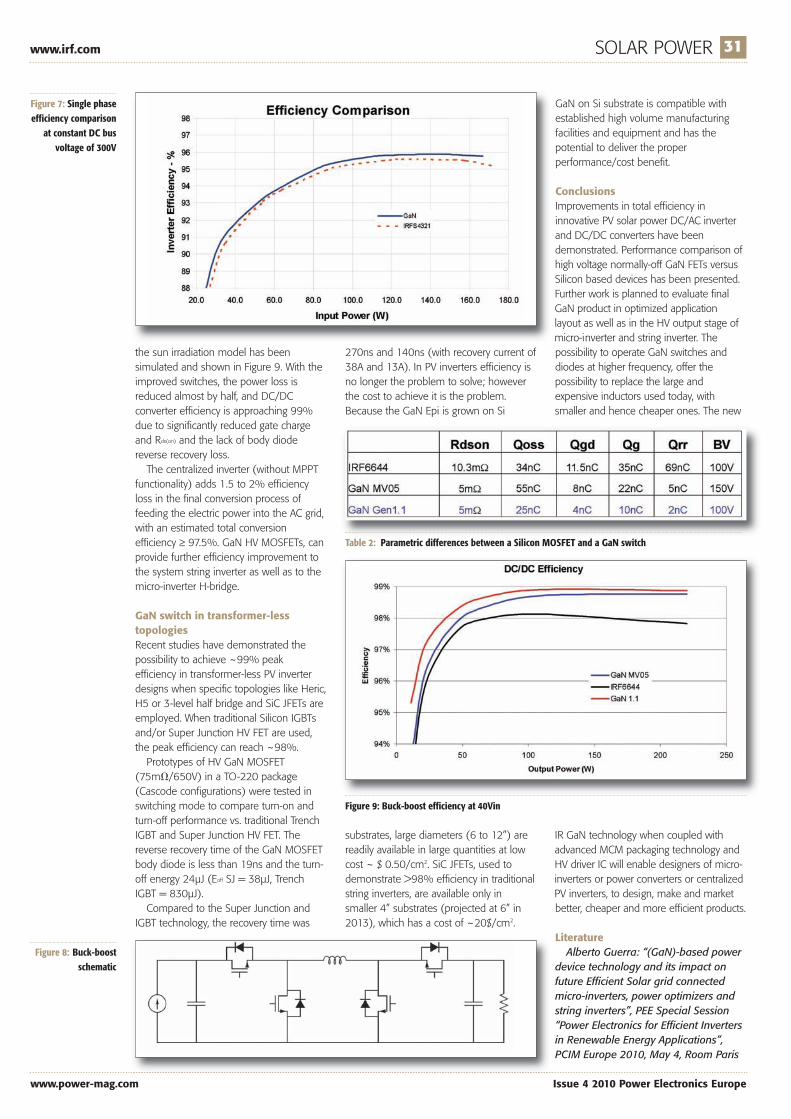
www.irf.com SOLAR POWER 31
www.power-mag.com Issue 4 2010 Power Electronics Europe
the sun irradiation model has beensimulated and shown in Figure 9. With theimproved switches, the power loss isreduced almost by half, and DC/DCconverter efficiency is approaching 99%due to significantly reduced gate chargeand Rds(on) and the lack of body diodereverse recovery loss.
The centralized inverter (without MPPTfunctionality) adds 1.5 to 2% efficiencyloss in the final conversion process offeeding the electric power into the AC grid,with an estimated total conversionefficiency ≥ 97.5%. GaN HV MOSFETs, canprovide further efficiency improvement tothe system string inverter as well as to themicro-inverter H-bridge.
GaN switch in transformer-lesstopologiesRecent studies have demonstrated thepossibility to achieve ~99% peakefficiency in transformer-less PV inverterdesigns when specific topologies like Heric,H5 or 3-level half bridge and SiC JFETs areemployed. When traditional Silicon IGBTsand/or Super Junction HV FET are used,the peak efficiency can reach ~98%.
Prototypes of HV GaN MOSFET(75m�/650V) in a TO-220 package(Cascode configurations) were tested inswitching mode to compare turn-on andturn-off performance vs. traditional TrenchIGBT and Super Junction HV FET. Thereverse recovery time of the GaN MOSFETbody diode is less than 19ns and the turn-off energy 24µJ (Eoff SJ = 38µJ, TrenchIGBT = 830µJ).
Compared to the Super Junction andIGBT technology, the recovery time was
270ns and 140ns (with recovery current of38A and 13A). In PV inverters efficiency isno longer the problem to solve; howeverthe cost to achieve it is the problem.Because the GaN Epi is grown on Si
substrates, large diameters (6 to 12”) arereadily available in large quantities at lowcost ~ $ 0.50/cm2. SiC JFETs, used todemonstrate >98% efficiency in traditionalstring inverters, are available only insmaller 4” substrates (projected at 6” in2013), which has a cost of ~20$/cm2.
GaN on Si substrate is compatible withestablished high volume manufacturingfacilities and equipment and has thepotential to deliver the properperformance/cost benefit.
ConclusionsImprovements in total efficiency ininnovative PV solar power DC/AC inverterand DC/DC converters have beendemonstrated. Performance comparison ofhigh voltage normally-off GaN FETs versusSilicon based devices has been presented.Further work is planned to evaluate finalGaN product in optimized applicationlayout as well as in the HV output stage ofmicro-inverter and string inverter. Thepossibility to operate GaN switches anddiodes at higher frequency, offer thepossibility to replace the large andexpensive inductors used today, withsmaller and hence cheaper ones. The new
IR GaN technology when coupled withadvanced MCM packaging technology andHV driver IC will enable designers of micro-inverters or power converters or centralizedPV inverters, to design, make and marketbetter, cheaper and more efficient products.
LiteratureAlberto Guerra: “(GaN)-based power
device technology and its impact onfuture Efficient Solar grid connectedmicro-inverters, power optimizers andstring inverters”, PEE Special Session“Power Electronics for Efficient Invertersin Renewable Energy Applications”,PCIM Europe 2010, May 4, Room Paris
Figure 7: Single phaseefficiency comparison
at constant DC busvoltage of 300V
Figure 8: Buck-boostschematic
Table 2: Parametric differences between a Silicon MOSFET and a GaN switch
Figure 9: Buck-boost efficiency at 40Vin
IRR Feature_Layout 1 03/06/2010 14:36 Page 31

Transfer Mold IPM forPhotovoltaic Application
32 SOLAR POWER www.mitsubishichips.com
Issue 4 2010 Power Electronics Europe www.power-mag.com
A new low loss large Dual In-line Package Intelligent Power Module with rating of 50A/600V is designed forphotovoltaic generation. It features a high heat dissipating insulation sheet, 5th generation CSTBT IGBTs andhigh output current driver IC leading to higher switching frequencies. Ming Shang, Hirofumi Oki,Kazuhiro Kuriaki, Toru Iwagami, Toshiya Nakano, Power Device Works, Mitsubishi ElectricCorporation, Fukuoka-City, Japan
Mitsubishi Electric manufactured the DualIn-line Package Intelligent Power Module(DIPIPMTM) with transfer mold structure from1997, and since that it has been adopted asthe inverter driver of appliances or industrial
motors. Low loss photovoltaic large DIPIPMis (PV DIPIPM) developed in respond of thecurrent, fast growing photovoltaic generationmarket (Figure 1) providing a good trade-offbetween efficiency and cost. Figure 2 showsa typical block diagram of a photovoltaicinverter. Here the DIPIPM is used as aDC/AC converter to convert the DCelectricity to AC electricity.
Improved IGBT structurePV DIPIPM adopts the Carrier StoredTrench-Gate Bipolar Transistor (CSTBTTM)chip with full gate structure, in order toimprove the trade-off relationship of on-state voltage and turn-off loss achieving aloss reduction of about 10% compared with
conventional CSTBT (plugged cell mergedCSTBT). Figure 3 shows the structure of fullgate CSTBT, Figure 4 the structure ofplugged cell merged CSTBT.
In a normal IGBT, the resistance of the n-
drift layer has to be kept high in order towithstand the blocking voltage at off-state.As the hole injection from collector to n-driftlayer at on-state, the resistance of the n-drift layer is reduced, and power loss isreduced. However, the resistance of the n-drift layer near emitter side is difficult todeduce because the hole density herebecomes low due to the far away distanceto the collector. Hence, it is difficult toachieve a very low on-state voltage.
CSTBT reaches a much lower on-statevoltage by the virtue of optimization of thehole density in the whole n- drift layer. Aspecial n barrier called n barred layer isdesigned under the P base layer to hinderthe holes injected from the collector frompenetrating to the emitter. This makes thefurther reduction of the on-state voltagepossible because hole density is increasedin the n-drift layer even near the emitterside. However, the major hurdle prevent fullgate CSTBT from being used in our pastdesign of DIPIPM are it’s large gate inputcapacitance and weak short-circuit withstandability which need a new driver IC waferprocess.
In order to reduce the input capacitance,conventional CSTBT was developed to bewith high current carrying capability,sometimes it is designed in a structure calledFigure 1: Photovoltaic 50A/600V DIPIPM with package size of 79mm x 31mm
Figure 2: Typical block diagram of photovoltaic generation system
Misubishi Feature_Layout 1 03/06/2010 14:40 Page 32
www.mitsubishichips.com WIND & SOLAR POWER 33
www.power-mag.com Issue 4 2010 Power Electronics Europe
plugged cell merged CSTBT so as to ensurea certain withstanding capability against shortcircuit failure (Figure 4). With this structurethe cell pitch is adjusted by ‘’plugging’’ someportion of the cells in a conventional highcell density device. The polysilicon in the‘’plugging’’ cell is connected to the emitterelectrode. Therefore, the CSTBT was not ableto use 100% of performance in thisstructure.Because the converter used for
photovoltaic generation system applies fastswitching, reducing the switching power losscould be a very effective way to enhance thewhole system efficiency. In order to achievean optimized trade-off relation between on-state voltage and turn-off loss, our PVDIPIPM adopted the fast full gate CSTBTchip combined with the advanced driver ICthat is capable to handle higher short circuitcurrent. Figure 5 shows the improvement ofthe trade-off between on-state voltage
Figure 3: Structure offull gate CSTBT
Figure 4: Structure ofplugged cell mergedCSTBT
Figure 5: Trade-offcharacteristic ofCSTBT
Misubishi Feature_Layout 1 03/06/2010 14:43 Page 33
34 SOLAR POWER www.mitsubishichips.com
Issue 4 2010 Power Electronics Europe www.power-mag.com
(VCE(sat)) and turn-off loss.The internal IC provides optimized drive
for the full gate CSTBT and realizes highfunction by means of the 0.5�m shrinkprocess technology. The traditional offsetstructured transistor has been finelyprocessed in the lateral direction bycombining shallow junction technologywhich increases the output capabilitywithout enlarging the chip size. Although
the full gate CSTBT needs larger drivecapability than a plugging cell, the fineprocess technology can realize an IC withhigh drive capability without sacrificing chipsize.
Circuit configuration and componentsThe internal circuitry of PV DIPIPM iscomposed of IGBTs and FWDs (FreeWheel Diode) in a two-phase inverterstructure together with control ICs, whichmake it different from normal large DIPIPMVer. 4. Figure 6 shows the internal blockdiagram of the PV DIPIPM.Control ICs realize functions such as
IGBT drive, under-voltage (UV) lockout,short circuit (SC) protection and fault signaloutput (FO). The output current of controlIC gate driver circuit is up to 5A ensuringhigh speed IGBT switching. When DIPIPM is used in fast switching
mode, a balanced operation of upper andlower arm power chips is difficult to beachieved. This is because the N-sideIGBT’s VGE could be significantly lowerthan the power supply VN1, due to theeffect of �V1 (�V1=Io×R), generated bythe shunt resistor (R) and �V2
(�V2=di/dt*L), generated by the parasiticinductance (L) of the external circuit.In order to minimize the side-effect of
�V1 and �V2, an extra control terminal pinVNS is internally connected to the emitter ofN-side IGBT (as is shown in Figure 6).Meanwhile, an external opto-coupler isneeded to maintain the isolation betweenpower GND and control GND, since theshort-circuit protection signal can not betaken directly by shunt resistor voltagesampling. External short-circuit protectioncircuit is shown in Figure 7. Experimentalresult has proved that switching power lossof IGBT chip was reduced 13% whencompared with non-VNS pin PV modules.
Loss simulationFigure 8 shows inverter loss simulationresult imitated two phases modulationsinusoidal waveform. This fast CSTBTreduced switching power loss comparedwith a conventional CSTBT leads to a 20%increase in efficiency.
ConclusionsA new low loss Photovoltaic DIPIPM in alarge package has been developed byapplying fast full gate CSTBT and itsoptimized drive IC, together with the high-efficient heat dissipating insulation sheet.
By adopting the high-speed full gateCSTBT, 10% of IGBT power loss wasreduced. By changing the drive circuit of N-side IGBT, since 13% of IGBT switchingloss reduction was realizable, 20% ofmodule total loss reduction was realized.
LiteratureShang Ming: “New Low loss Transfer
Mold IPM for Photovoltaic Generation”,PEE Special Session “Power Electronicsfor Efficient Inverters in RenewableEnergy Applications”, PCIM Europe 2010,May 4, Room Paris
Figure 6: Internal block diagram of Photovoltaic DIPIPM
Figure 7: Short circuitprotection circuit ofPhotovoltaic DIPIPM
Figure 8: Power loss comparison (Conditions:Tj=125_, Vcc=380V, VD=15V, Io=15Arms, PF=0.95,fsw=15.5kHz)
Misubishi Feature_Layout 1 03/06/2010 14:40 Page 34

35_PEE_0410_35_PEE_0410 03/06/2010 14:45 Page 1

Name:
Company Name:
Address:
Postcode: Email:
Tel: Total Number of Copies @ £ p+p Total £
Drives S & S Hyd H/B Pne H/B Ind Mot CompH/B H/B Air
QUANTITY QUANTITY
Drives&Controls
There are now 6 handy reference books available at only £4.99 each from the publishers of Drives & Controlsand Hydraulics & Pneumatics magazines.
Published in an easily readable style and designed to helpanswer basic questions and everyday problems withoutthe need to refer to weighty textbooks, we believe you’llfind them invaluable items to have within arms reach.
From the publishers of
QUANTITY QUANTITY QUANTITY
If you would like to obtain additional copies of the handbooks, please complete the form below and either fax it on 01732 360034 or post your order to:Engineer’s Handbook, DFA MEDIA LTD, Cape House, 60a Priory Road, Tonbridge, Kent TN9 2BL.
You may also telephone your order on 01732 370340
Cheques should be made payable to DFA MEDIA LTD and crossed A/C Payee.
Discounts are available for multiple copies. 2-5 copies £4.30, 6-20 copies £4.10, 20+ copies £3.75.
Postage and Packaging: 1-3 copies £2.49, 4 copies and over £3.49
PLEASE ALLOW UP TO 28 DAYS FOR DELIVERY
QUANTITY
PRACTICAL ENGINEER’S HANDBOOKS
HYDRAULICS
INDUSTRIALMOTORS
SERVOSAND STEPPERS
PNEUMATICS
COMPRESSED AIR
INDUSTRIAL ELECTRIC DRIVES
Hydraulics&Pneumatics
k
ONLY
£4.99 EACH
36_PEE_0410_36_PEE_0410 03/06/2010 16:07 Page 1

PRODUCT UPDATE 37
www.power-mag.com Issue 4 2010 Power Electronics Europe
MAKING MODERN LIVING POSSIBLE
DANFOSS SILICON POWER
SILICONPOWER.DANFOSS.COM
The coolest approach to heat transferBenefit from the most cost-efficient power modules available
It cannot be stressed enough: Efficient cooling is the most important feature in regards to Power Modules. Danfoss Silicon Power’s cutting-edge ShowerPower® solution is designed to secure an even cooling across base plates, offering extended lifetime at no increase in cost. All our modules are customized to meet the exact requirements of the application. In short, when you choose Danfoss Silicon Power as your supplier you choose a thoroughly tested solution with unsurpassed power density.
Please go to siliconpower.danfoss.com to learn about Power Modules that are second to none.
ShowerPower®
900A Current Transducer LEM hasintroduced itsnew ITL 900currenttransducerbased on adouble fluxgateclosed looptechnology forprecisemeasurementof DC, AC andpulsed currentsup to ±900A. Itprovideslinearity error of3ppm over anoperating temperature range of 10°C to 50ºC, offset stability over four hours ofless than 0.5ppm, and offset current temperature coefficient of less than0.3ppm/K. With a wide measurement bandwidth of more than 200kHz (-3dB) fast current transients can be accurately measured. Other advantagesinclude negligible self-magnetisation, a current overload capability, and galvanicisolation between the high-power primary circuit and the electronic secondarycircuit. The ITL 900 works on an internal clock that can also be synchronisedto an external clock signal, increasing immunity to periodic noise.
www.lem.com
STMicroelectronics has introduced an intelligent power switch (IPS) for use inindustrial controls, which provides improved accuracy to minimize energy lossesand prevent system errors when faults occur. This new two-channel IC in 6mmx 5mm footprint integrates all the necessary logic, driver circuitry, power stage,protection, and diagnostic functions. The chip’s inputs are 3.3V TTL/CMOScompatible; its outputs are connected in the high-side configuration; and twoindependent resistive, inductive or capacitive loads can be driven. The chip’s built-in shorted-load protection with independent active current
limitation for each channel prevents load faults from pulling down the systempower supply. If either channel becomes overloaded that channel is turned offindependently while the other continues operating normally, and it is restartedautomatically when the junction temperature has returned to normal. If bothchannels are overloaded, they are restarted non-simultaneously to avoiddrawing high peak currents from the power supply. Other features helpingdesigners to deliver rugged, highly featured solutions include protection against
loss of ground,as well asdiagnosticssuch as open-load detectionin the off state.The deviceoperates at 9Vto 36V supplyvoltage andnominalcurrent of 0.5Aper channel.
www.st.com
Power Switch for Industrial Applications
Product Pages_Layout 1 03/06/2010 14:49 Page 37

38 PRODUCT UPDATE
Issue 4 2010 Power Electronics Europe www.power-mag.com
LED Driver with DynamicHeadroom ControlNational Semiconductor announceda LED driver with dynamic headroomcontrol and multiple outputs forhigh-power applications that drivesup to four strings of LEDs. TheLM3464 is a high-voltage currentcontroller with four individual currentregulator channels. It works inconjunction with external N-channelMOSFETs and sense resistors toaccurately drive current to each LEDstring. The LM3464 features a wideinput voltage range up to 80V todrive multiple LEDs per string. Athermal foldback feature protects theLEDs from unsafe temperatures thatcan significantly degrade the lightoutput or lifetime of the LEDs.During an over-temperaturecondition, the thermal foldbackreduces the current through theLEDs until the LED junctiontemperature of the LEDs returnsback to a safe operatingtemperature. This user-programmable feature allows for amore robust and reliable thermaldesign, helping to ensure the lifetime
and light output of the LEDs overtime and through temperaturevariances due to environmentalconditions of the fixture. Thedynamic headroom control featuremonitors the forward voltages of theLED strings and dynamically adjuststhe LED supply voltage through the
power supply feedback to the lowestlevel required. By directly controllingthe output of the offline regulator,the LM3464 can eliminate thesecond stage switching regulatorcommonly required for offline LEDpower supplies. The device featuresboth pulse-width modulation (PWM)
and analog dimming interfaces toallow the user to select betweenvarious dimming types for differentapplications. The LM3464 is pricedat $4.50 in 1,000-unit quantities.
www.national.com/pf/LM/LM3464.html
CISSOID released their new EREBUS(tm)buck DC/DC converters operating from -55°Cto +225°C. EREBUS can step input voltagesfrom 12V to 50V down to an output voltageadjustable from 10% to 90% of the input.These converters demonstrate efficiencies inexcess of 85% above 200°C. Whenconfigured as synchronous DC/DC converter,it operates in Continuous Current Mode(CCM) at a constant frequency, making ripplefiltering easier for demanding sensorapplications and uses the soft-start capabilityof a PWM controller to enable a smoothstart-up. The input voltage feed forwardcompensation makes it very robust to inputvoltage transient variations and provides a DC
line regulation better than ±1.5mV/V. Thedemonstration board, adjusted to a 5Voutput, is available in two versions, for amaximum input voltage of 40V or 50V. It candeliver up to 70W at 225°C. The boards arerated to 175°C but can sustain shortexcursion to 225°C. EREBUS technology canbe used to build DC/DC buck converterswith output voltages up to 45V anddelivering up to 180W (280W for Vin <40V).The reference design and its active bill-of-material can be mapped onto hightemperature substrates and assembled inhigh reliability modules.
www.cissoid.com
High Temperature DC/DC Converter Platform
To receive your own copy of
subscribe today at:
www.power-mag.com
Product Pages_Layout 1 03/06/2010 14:49 Page 38

PRODUCT UPDATE 39
Higher OperatingTemperatures forBipolar ModulesIXYS announced a new package generation called Simbus A for itsphase-leg rectifier module range featuring spring contacts forsolder-free connection of the control board and a maximumjunction temperature of 140°C. The first products are a set of three1600V phase-leg rectifier topologies. The dual thyristor module“MCMA200P1600SA” features two thyristors of 200A rating inphase leg topology and will be followed by the dual diode version“MDMA200P1600SA” and the thyristor/diode combination“MCMA200PD1600SA” for a more flexible circuit requirement. TheSimbus A also includes IXYS` Direct Copper Bonded (DCB)substrates that allow the user 4800V isolation voltage fromterminals to heatsink.A common application for the Simbus A isthe input bridge rectification for AC or DC motor control with 230VAC mains supply.
www.ixys.com
Ultracapacitors upto 3000 FaradsAbout the size of a can of soda, K2 Series BOOSTCAP® cell operates at 2.7V.Primary applications for Maxwell’s products (cells range from 650 to 3,000F)include automotive subsystems, hybrid and electric vehicle drive trains,renewable energy systems, back-up power, grid stabilization, electric railsystem power and many other transportation and industrial applications thatrequire burst power and heavy cycling (which cannot be efficiently provided bya battery or power supply alone). These new ultracapacitors also work inparallel with batteries for applications that require both a constant low powerdischarge capability (for continual function) and a pulse power capability (forpeak loads). In these applications, the ultracapacitors relieve the batteriesduring peak load periods. This in turn results in an extension of battery life(longer use before replacement), reduced battery maintenance requirements,
and a reduction of overall battery sizeand cost. Individual K2 cells (inproduction volumes) are nowavailable as well as multi-cell
modules from RichardsonElectronics with workingvoltage ranging from 16V to125V.
www.rell.com/RFPD
www.power-mag.com Issue 4 2010 Power Electronics Europe
Product Pages_Layout 1 03/06/2010 14:49 Page 39

40 PRODUCT UPDATE
Issue 4 2010 Power Electronics Europe www.power-mag.com
Texas Instruments’ new TPS63020 power management IC features up to96% efficiency. The buck-boost device operates with a wide input voltage range of 1.8V to
5.5V and can discharge lithium batteries down to 2.5V or lower, whilemaintaining light load efficiency. The single-inductor, 2.4MHz convertercomes in a 3mm x 4mm x 1mm package, and can achieve a completeDC/DC converter solution of 100 mm_. Key features of the device includehigh output current capability allows a battery-powered device to generatethe most current with the greatest amount of efficiency; for example, 3A at3.3V in step-down mode and more than 2.0A at 3.3V in boost mode attypical conditions; dynamic input current limit effectively protects the circuitand system; power save mode maintains high efficiency at light load, and itsupports one-cell lithium-based or 2- or 3-cell Alkaline, NiCd or NiMHbatteries. The TPS63020 and a 3.3V fixed output voltage version, theTPS63021, are available in volume with a suggested resale price of $2.50 in
4A Buck-Boost Converter
1,000-unit quantities. Samples, evaluation modules and application notesare available.
www.ti.com/tps63020-preu
CAPZero ICs Safely Discharge X Capacitors
Power Integrations’ new CAPZero is a two-terminal, automatic X capacitordischarge IC that eliminate power losses while allowing power supplies tocomply with safety standards. X capacitors are typically positioned across apower supply’s input terminals to filter differential EMI noise. Alone, these
components could present a safety hazard because they can store unsafelevels of high-voltage energy for long periods of time after the AC isdisconnected. To meet safety standards, resistors are commonly used inparallel with the X capacitor and across the AC line to provide a discharge path.However, these discharge resistors produce a constant power loss while theAC is connected and are a significant contributor to no-load and standby inputpower consumption. CAPZero acts as a smart high-voltage switch whenplaced in series with discharge resistors. When AC voltage is applied, CAPZeroblocks current flow in the X capacitor safety discharge resistors, reducing thepower wasted in these components to zero at 230 VAC. When the AC voltageis disconnected, CAPZero automatically and safely discharges the X capacitorby closing the circuit through the bleed resistors and directing the energy awayfrom the exposed AC plug. CAPZero is suitable for all AC/DC converters with Xcapacitors that require very low standby power, and is offered with 825V or1000V MOSFETs to support a variety of power supply design needs for a widerange of applications, including appliances requiring EuP Lot 6 compliance andadapters requiring ultra-low no-load consumption. CAPZero devices areavailable in an SO-8 package at $0.40 each for 10,000-piece quantities.
www.powerint.com/lp/capzero
Application Schematic-07LXMG221WW-0700034-D0
Application Schematic-0700034-D0
Microsemi announced the first product in aplanned family of solutions designed to provideoptimized power conversion and lightmanagement for solid state lighting fixtures,enabling the energy and lifetime cost savingspromise of LED-based illumination. Novelfeatures that can be optimally offered by LEDlighting include perfectly tuned and personalizedlight via light intensity and light color controls, aswell as reliable integration into smart power andlighting networks starting to appear in theresidential, office and commercial space. All ofthese will only be possible with smart andoptimized LED drivers. Designated theLXMG221W-0700034-D0, the power supplymodule supports 5 to 16 LEDs and will bejoined by a portfolio of solid state lightingproducts in the coming months. Its universal
input voltage range of 90 to 305V AC enablesoperation in 100, 120, 220-240 and 277V AC,50Hz and 60Hz systems. The module provides90% power conversion peak efficiency whiledelivering non-flickering dimming down to 10%.The module can be easily integrated intodimming and non-dimming fixtures and meetsrequirements for both commercial andresidential applications, including its pending CEand UL1310 certification. Its compact, IP66-rated plastic package protects the power supplyfrom dust and temporary water exposure andoffers a thru-hole for more secure mounting.The LXMG221W-0700034-D0 is in pre-production. Samples are available with pricingfor individual samples at $60.
www.microsemi.com
Driver Module for LED Light Fixtures
Product Pages_Layout 1 03/06/2010 14:49 Page 40

WEBSITE LOCATOR 41
www.power-mag.com Issue 4 2010 Power Electronics Europe
AC/DC Connverters
www.irf.comInternational Rectifier Co. (GB) LtdTel: +44 (0)1737 227200
Diodes
Discrete Semiconductors
Drivers ICS
www.microsemi.comMicrosemiTel: 001 541 382 8028
Fuses
GTO/Triacs
Hall Current Sensors
IGBTs
DC/DC Connverters
DC/DC Connverters
www.irf.comInternational Rectifier Co. (GB) LtdTel: +44 (0)1737 227200
www.power.ti.comTexas InstrumentsTel: +44 (0)1604 663399
www.power.ti.comTexas InstrumentsTel: +44 (0)1604 663399
www.neutronltd.co.ukNeutron LtdTel: +44 (0)1460 242200
Harmonic Filters
www.murata-europe.comMurata Electronics (UK) LtdTel: +44 (0)1252 811666
Direct Bonded Copper (DPC Substrates)
www.curamik.co.ukcuramik� electronics GmbHTel: +49 9645 9222 0
www.irf.comInternational Rectifier Co. (GB) LtdTel: +44 (0)1737 227200
www.mark5.comMark 5 LtdTel: +44 (0)2392 618616
www.mark5.comMark 5 LtdTel: +44 (0)2392 618616
www.dgseals.comdgseals.comTel: 001 972 931 8463
www.microsemi.comMicrosemiTel: 001 541 382 8028
www.irf.comInternational Rectifier Co. (GB) LtdTel: +44 (0)1737 227200
www.digikey.com/europeDigi-KeyTel: +31 (0)53 484 9584
www.irf.comInternational Rectifier Co. (GB) LtdTel: +44 (0)1737 227200
www.mark5.comMark 5 LtdTel: +44 (0)2392 618616
www.irf.comInternational Rectifier Co. (GB) LtdTel: +44 (0)1737 227200
www.protocol-power.comProtocol Power ProductsTel: +44 (0)1582 477737
Busbars
www.auxel.comAuxel FTGTel: +44 (0)7714 699967
Capacitors
Certification
www.powersemiconductors.co.ukPower Semiconductors LtdTel: +44 (0)1727 811110
www.powersemiconductors.co.ukPower Semiconductors LtdTel: +44 (0)1727 811110
Connectors & Terminal Blocks
www.auxel.comAuxel FTGTel: +44 (0)7714 699967
www.productapprovals.co.ukProduct Approvals LtdTel: +44 (0)1588 620192
p49-50 Website Locator_p41-42 Website Locator 03/06/2010 15:00 Page 41

42 WEBSITE LOCATOR
Issue 4 2010 Power Electronics Europe www.power-mag.com
Power Modules
Power Protection Products
Power Substrates
Resistors & Potentiometers
RF & Microwave TestEquipment.
Simulation Software
Thyristors
Smartpower Devices
Voltage References
Power ICs
Switches & Relays
Switched Mode PowerSupplies
Switched Mode PowerSupplies
Thermal Management &Heatsinks
www.irf.comInternational Rectifier Co. (GB) LtdTel: +44 (0)1737 227200
www.rubadue.comRubadue Wire Co., Inc.Tel. 001 970-351-6100
www.irf.comInternational Rectifier Co. (GB) LtdTel: +44 (0)1737 227200
www.irf.comInternational Rectifier Co. (GB) LtdTel: +44 (0)1737 227200
www.mark5.comMark 5 LtdTel: +44 (0)2392 618616
www.irf.comInternational Rectifier Co. (GB) LtdTel: +44 (0)1737 227200
www.irf.comInternational Rectifier Co. (GB) LtdTel: +44 (0)1737 227200
www.power.ti.comTexas InstrumentsTel: +44 (0)1604 663399
www.auxel.comAuxel FTGTel: +44 (0)7714 699967
www.irf.comInternational Rectifier Co. (GB) LtdTel: +44 (0)1737 227200
www.mark5.comMark 5 LtdTel: +44 (0)2392 618616
www.microsemi.comMicrosemiTel: 001 541 382 8028
www.power.ti.comTexas InstrumentsTel: +44 (0)1604 663399
www.ar-europe.ieAR EuropeTel: 353-61-504300
www.power.ti.comTexas InstrumentsTel: +44 (0)1604 663399
www.power.ti.comTexas InstrumentsTel: +44 (0)1604 663399
www.universal-science.comUniversal Science LtdTel: +44 (0)1908 222211
www.power.ti.comTexas InstrummentsTel: +44 (0)1604 663399
www.curamik.co.ukcuramik� electronics GmbHTel: +49 9645 9222 0
www.dau-at.comDau GmbH & Co KGTel: +43 3143 23510
www.denka.co.jpDenka Chemicals GmbHTel: +49 (0)211 13099 50
www.lairdtech.comLaird Technologies LtdTel: 00 44 1342 315044
www.power.ti.comTexas InstrummentsTel: +44 (0)1604 663399
www.universal-science.comUniversal Science LtdTel: +44 (0)1908 222211
www.universal-science.comUniversal Science LtdTel: +44 (0)1908 222211
www.isabellenhuette.deIsabellenhütte Heusler GmbH KGTel: +49/(27 71) 9 34 2 82
ADVERTISERS INDEX
AR Europe 7
Cornell Dubilier 9
CT Concepts IBC
CWIEME 39
Danfoss 37
Dau
DFA Media Ltd 36
Digikey IFC
Fischer 33
Fuji 35
HKR GmbH 17
Infineon 4
International Rectifier OBC
Isabellenhutte 18
Ixys 29
Microsemi Power 23
The Bergquist Company 19
Toshiba Europe 21
Mosfets
Magnetic Materials/Products
Optoelectronic Devices
www.power.ti.comTexas InstrumentsTel: +44 (0)1604 663399
Packaging & Packaging Materials
www.curamik.co.ukcuramik� electronics GmbHTel: +49 9645 9222 0
www.irf.comInternational Rectifier Co. (GB) LtdTel: +44 (0)1737 227200
www.neutronltd.co.ukNeutron LtdTel: +44 (0)1460 242200
www.microsemi.comMicrosemiTel: 001 541 382 8028
www.mark5.comMark 5 LtdTel: +44 (0)2392 618616
www.biaspower.comBias Power, LLCTel: 001 847 215 2427
www.digikey.com/europeDigi-Key Tel: +31 (0)53 484 9584
www.power.ti.comTexas InstrumentsTel: +44 (0)1604 663399
www.digikey.com/europeDigi-Key Tel: +31 (0)53 484 9584
www.irf.comInternational Rectifier Co. (GB) LtdTel: +44 (0)1737 227200
www.power.ti.comTexas InstrumentsTel: +44 (0)1604 663399
www.neutronltd.co.ukNeutron LtdTel: +44 (0)1460 242200
www.microsemi.comMicrosemiTel: 001 541 382 8028
www.mark5.comMark 5 LtdTel: +44 (0)2392 618616
p49-50 Website Locator_p41-42 Website Locator 03/06/2010 15:00 Page 42
5

New High Power Driver
Launching the next generation of high voltage IGBT gate drivers, CONCEPT introduces two new top # � & � � ( � � � % # � � ( ( 1SP0635 and 1SP0335 - with an outstanding performance to cost ratio. Consequent integration enables cost down by 40%
2C) assures excellent electrical performance and
-vers are the perfect choice for high performance traction application, high power inverter and medium voltage drives.
Features
2CGate voltage monitoring
2-level and multilevel topologies
Long service life
www.IGBT-Driver.com
SAMPLES AVAILABLE!
CT-Concept Technologie AG, Renferstrasse 15, CH-2504 Biel, Switzerland, Phone +41-32-344 47 47
Undisputed Competence!
Paralleling with 1SP0335
43_PEE_0410_43_PEE_0410 03/06/2010 15:31 Page 1

Part Number Voltage & ShuntTypical
Load(W)
Io @ TC = 100°C
(A RMS)Package Confi guration
IRAM136-0461G 600V, Integr. Shunt 300W 2
SIP-1
3-phase, 600V + Input bridge
IRAMS06UP60A 600V Open Emitter400W 3
IRAMS06UP60B 600V Integr. Shunt
IRAM136-0760A 600V Open Emitter 400W 3.5
SIP-05IRAM136-1060A 600V Open Emitter 750W 5
IRAM136-1060B 600V Int. Shunt 750W 5
3-phase, 600V
IRAM136-1061A 600V Open Emitter 750W 5 SIP-1A
IRAMS10UP60A 600V Open Emitter750W 5 SIP-1
IRAMS10UP60B 600V Integr. Shunt
IRAMX16UP60A 600V Open Emitter 1500W 8
SIP-2IRAMX16UP60B 600V Integr. Shunt
IRAMX20UP60A 600V Open Emitter 2500W 10
IRAMY20UP60B 600V Integr. Shunt
SIP-3IRAM136-3063B 600V Integr. Shunt 3000W 15
IRAM136-3023B 150V Integr. Shunt 750W 15 3-phase, 150V
IRAM336-025SB 500V Integr. Shunt 200W 1SIP-S
3-phase, 500V
IRAM109-015SD 500V No Shunt 200W 1 H-Bridge
UPowerSupply
EMIFilter +PFC
DIGITAL CONTROLLER
HIGH VOLTAGE GATE DRIVER IC
V W
POWER MODULE
RectifierBridge
AC line MOTOR
Integrated bootstrap diode
Rugged 600V high voltage IC with integrated protection features
High effi ciency, rugged 600V IGBT
Built-in over temperature protection
Built-in over current protection
Minimized EMI due to controlled slew rate
Features
• Utilizes proprietary three-phase monolithic gate driver IC matched with highly effi cient IGBT power switches
• Insulated metal substrate technology for reduced EMI
• Optimized for power up to 3kW
• Web-based design tool at www.irf.com/design-center/ipm
• Replaces more than 20 discrete parts to deliver complete power stage solution
IR’s iMOTION brings digital controllers, analog stage and power modules together in one easy to implement, integrated design platform.
for more information call + 49 (0) 6102 884 311 or visit us at www.irf.com
With IR’s IRAM integrated power modules
IR’s iMOTION (ai mo shan), representing the intelligent motion control Motion Control Engine and Analog Signal Engine, are trademarks of International Rectifi er
Protect and Simplify Your Design
THE POWER MANAGEMENT LEADER
44_PEE_0410_44_PEE_0410 03/06/2010 15:33 Page 1