new approaches for high-efficiency solar cells: final … of algaas to 100 i ... the goal is to...
TRANSCRIPT

December 1997 • NREL/SR-520-23266
New Approach for High-Efficiency lar Cells Final Report
S.M. Bedair and N.A. El-Masry North Carolina State University Raleigh, North Carolina
National Renewable Energy Laboratory 1617 Cole Boulevard Golden, Colorado 80401-3393 A national laboratory of the U.S. Department of Energy Managed by Midwest Research Institute for the U.S. Department of Energy under Contract No. DE-AC36-83CH10093

---� ); r-----------------------�
i I
l .1
I j
.J
\ �
NREL/SR-520-23266 • UC Category: 1260
New Approach for -High-Efficiency - lar Cells -
Final Report
S.M. Bedair and N.A. El-Masry North Carolina State University Raleigh, North Carolina
NREL technical monitor: R. McConnell
National Renewable Energy Laboratory 1617 Cole Boulevard Golden, Colorado 80401-3393 A national laboratory of the U.S. Department of Energy Managed by Midwest Research Institute for the U.S. Department of Energy under Contract No. DE-AC36-83CH10093
Prepared under Subcontract No. XDA-3-12114-5 December 1997
�------------------�

This publication was reproduced from the best available camera-ready copy
submitted b)' the subcontractor and received no editorial review at NREL.
NOTICE
This report was prepared as an account of work sponsored by an agency of the United States government. Neither the United States government nor any agency thereof, nor any of their employees, makes any warranty, express or implied, or assumes any legal liability or responsibility for the accuracy, completeness, or usefulness of any information, apparatus, product, or process disclosed, or represents that its use would not infringe privately owned rights. Reference herein to any specific commercial product, process, or service by trade name, trademark, manufacturer, or otherwise does not necessarily constitute or imply its endorsement, recommendation, or favoring by the United States government or any agency thereof. The views and opinions of authors expressed herein do not necessarily state or reflect those of the United States government or any agency thereof.
Available to DOE and DOE contractors from: Office of Scientific and Technical Information (OSTP.O. Box62
Oak Ridge, TN 37831 Prices available by calling (423) 576-8401
Available to the public from: National Technical Information Service (NTIS) U.S. D epartment of Commerce
5285 Port Royal Road Springfield, VA 22161
n � (703) 487-4650
n
I)
1i #".
t • .: Printed on paper containing at least 50% wastepaper, including 20% postconsumer waste

TABLE OF CONTENTS
1 I
I I
j
�] J
I. Summary . . . . . . . . . . . . . . . . . . . . . . . . . . . . . . . . . . . . . . . . . . . . . . . . . . . . . . . . . . . . . . 1
II. Graduate Students and their Thesis Highlights . . . . . . . . . . . . . . . . . . . . . . . . . . . . . . . . . . 1
ill. Technical Contents . . . . . . . . . . . . . . . . . . . . . . . . . . . . . . . . . . . . . . . . . . . . . ... . . . . . . 3
Atomic Layer Epitaxy ofDevice Quality AlGaAs and AlAs . . . . . . . . . . . . . . . . . . . . . . . . . . . . 7
Selenium Doping of GainP by Atomic Layer Epitaxy . . . . . . . . . . . . . . . . . . . . . . . . . . . . . . . . 21
Al 3�_7As/GaAs Heterojunction Tunnel Diode for Tandem Solar Cell Applications0 . . . . . . . 25
Effect of Strain and Heavy Doping on G� In _�/Ga_5/ln_4;p Band Structure for1BSF and Window Layer Applications . . . . . .. . . . . . . . . . . . . . . . . . . . . . . . . . . . . . . . . 33
Back Surface Fields for nip and p/n GainP Solar Cells . . . . . . . . . . . . . . . . . . . . . . . . . . . . . . . 61
Properties ofHighly Strained GaP and GaP/GaAs/GaP Quantum Wells Grown on GaAs Substrates by Atomic Layer Epitaxy . . . . . . . . . . . . . . . . . . . . . . . . . . . . . . . . 64
AlGaAs/GainP Heterojunction Tunnel Diode. . .................................... 86

\
i I. Summary
This report summarizes the activities carried out in this subcontract. These activities cover, first
the atomic layer epitaxy (ALE) growth of GaAs, AlGaAs and InGaP at fairly low growth
temperatures. This was followed by using ALE to achieve high levels of doping both n-type and
p-type required for tunnel junctions (Tj) in the cascade solar cell structures. Then we studied the
properties of AlGaAs/InGaP and AlGaAs/GaAs tunnel junctions and their performances at
different growth conditions. This is followed by the use of these tunnel junctions in stacked solar
cell structures. The effect of these tunnel junctions on the performance of stacked solar cells was
studied at different temperatures and different solar fluences. Finally, we studied the effect of
different types of back surface fields (BSF), both pin and nip GalnP solar cell structures, and their
potential for window layer applications. Parts of these activities were carried in close
cooperations with Dr. Mike Timmons of the Research Triangle Institute.
r
) j l
J
l
n. Graduate Students and their Thesis high lights:
Three graduate students Ph.D. theses were supported by this subcontract. Copies of there theses
are available upon request.
1) Donggeun Jung- Ph.D. (1993)
The thesis has both experimental and modeling parts.
I. Experimental
• Growth of GaAs.by ALE in a prototype reactor2
• C-doping of AlGaAs to 10 0 I cm3• Low temperature growth oflnGaP by ALE in the range 400-500 °C• Se doping oflnGaP- 9x10¹⁹ I cm3• Properties of tunnel junctions in the AlGaAs/InGaP material systems.• Effect of Annealing on the tunnel junction properties.
1

11. Modeling
• Band line-up of the AlGaAs!InGaP heterointerfaces• Modeling of T .j. I-V characteristics• Effect of depletion layer thickness on peak current in T.j.• Dopants diffusion in annealed T.j.
2) Jamal Eldallal - Ph.D. (1994)
Thesis contains three major parts.
I. ALE Development in a Semiproduction Reactor
• Conditions for monolayer I ALE cycle• Low background carrier concentrations• n+- type doping using silane- 1019 I cm3• High growth rate of2 J.lm I h in multi-wafer reactor (3 wafer, 2" diameter)
2• p-type carbon doping - 10 0 I cm3 in AlGaAs
11. p+- AlGaAsln+- GaAs Tunnel Junction
• I-V characteristics• Dependence of peak currents on growth conditions
m. GaAs/AlGaAs Tandem Cells and their performances
• Temperature effects• High solar concentration effects
3) Nadia Rafat- Ph.D. (1995)
The thesis contains experimental and modeling activities.
I. Experimental
Ji • Growth and characterization of GalnP 2, top cell lattice matched to GaAs
substrate
r_J! • Study the effect of BSF on pin and n/p structures• Compare the performances of abrupt GainP 2, graded GainP 2 and AlGaAs BSF
layers
2
: � '

11. Modeling
• Bandgap calculations to study the bandgap line up in Gao.siOo.sP I G�In1_�material systems
• Study the effect of strain and doping levels on this bandgap line up• Study band line up for window layers including different material systems such as
lfixGa1.� and GaP thin films
m. Technical Contents
Activities were carried along the following six research directions.
I) Atomic Layer Epitaxy of Device Quality AIGaAs and AlAs
Atomic layer epitaxy (ALE) of device quality AIGaAs and AlAs has been demonstrated on
a modified commercial metalorganic vapor phase epitaxial (MOVPE) reactor with a rotating
susceptor. Growth rates up to 2 11m I ·h were achieved in this reactor AlAs had a much narrower
plateau of saturated growth as compared to GaAs and Al0_ .7As, which many be due to the
higher Al-CH bond energy. This growth rate is comparable to that ofMOCVD, however, the3
thickness is controlled to the monolayer level.
2) Selenium Doping of GainP by Atomic Layer Epitaxy
Selenium doping ofGainP was performed using atomic layer epitaxy. The dependence of
the n-type carrier concentration of Se-doped GainP on growth temperature was quite different
from that of Se-doped GaAs. Reducing growth temperature was found to be a crucial factor in
achieving high n-type doping levels in as-grown Se-d oped GainP. Carrier concentrations in the
high I 019 I 3 cm was achieved.
3Gao
'i
3

3
3
3Qa.o.7As
3) Alo.3Ga.o.7As/GaAs Heterojunction Tunnel Diode for Tandem Solar Cell Applications
A p+- Al0_3Ga.o.7Asln+-GaAs heterojunction tunnel diode was fabricated using an Atomic
0 Layer Epitaxy (ALE) growth technique. Background carbon doping of- 102 cm· was achieved
in the p-side of the diode by optimizing growth conditions such as the VIII! ratio, exposure times
to reactant gases, and growth temperature. In the n - side of the diode, GaAs was doped with
1silane and doping concentrations as high as 7xl0 8 cm· were also achieved. The dopants are
chosen to satisfy the high levels and low diffusion requirements. ALE grown p+- Al0_ I n+
-GaAs heterojunction tunnel diodes showed high peak current density of 40 A I cm2 and a high
peak-to-valley ratio of 10. The diode can be used to interconnect the high and low band-gap cells
in the AlGaAsiGaAs cascade solar cell structure. The reactor used in this investigation is a
commercial MOCVD system which has been specially modified for dual operation of ALE and
MOCVD growth modes.
4) Effect of Strain and Heavy Doping on G<txin1_xPIGa.o.51Ino.4;p Band Structure for BSF andWindow Layer Applications
We have carried out bandgap calculations to study the bandgap line-up in the
Ga.o.sino.sPIG<txin1_J> material system. The goal is to determine t:lEc and L1Ev and thus the potential
applications ofG<txln1_x P (x>0.5) both as a BSF window layer, for pi n and n/p structures. In
these calculations the following factors were considered:
I) effect of strainii) effect of heavy doping.
Strain effects were studied using both Van de Walle's and Hrivnak's models. Effective mass data
were obtained using the Krijn approach. These calculations were first applied to the strained
GalnAs ternary alloy and results compared favorably to the available experimental data for this
4

system.
5) Back Surface Fields for ni p and p/ n GainP Solar Cells
We have grown n/ p/ p + GainP 2 top cells, lattice matched to GaAs for multijunction tandem
solar cells. We have studied the, effect of different types of back surface field (BSF) layers on the
cell parameters of each cell. These layers are namely, abrupt strained GalnP2, graded strained
GainP 2, disordered GalnP 2 and AlGaAs layers. The measurements were done under 1-sun AMO
spectrum. The results show that the abrupt strained GalnP2 BSF outperforms the disordered
GalnP2 BSF. Likely related to material quality, the AIGaAs layer clearly produce the least
efficient BSF. It has been found that the abrupt strained Ga,Jn _xp BSF with x=0.56 gives better1
results than the case with x=0.63 for the p/ n/ n+ structure.
6) AIGaAs/GalnP Heterojunction Tunnel Diode for Cascade Solar Cell Application
A p+- AIGaAs/ n+-GainP heterojunction tunnel diode with bandgap Eg z 1.9 eV was
2 1fabricated by atomic layer epitaxy growth. Doping levels of 1xl0 0 cm·3 and 5x10 9 cm·3 were
achieved in the p and n side of the diode using carbon and selenium, respectively. The diode can
be used to interconnect the high and low band-gap cells in the AIGaAs/GaAs cascade solar cell
2structure. For forward current of20 Ncm , which is the expected current density at 1000 suns
operation, there is only - 20 m V voltage drop across the tunnel junction. When annealed at 650
and 750 octo simulate the growth of the top cell, the diode was still suitable for 1000 suns
operation. This is the first reported tunnel diode fabricated in high band-gap material systems that
can be used as the connecting junction in the cascade solar cell structure operating at 1000 suns.
'!
I' I
5

7) Properties of Highly Strained GaP and GaP/GaAs/GaP Quantum Wells Grown on GaAsSubstrates by Atomic Layer Epitaxy
Atomic layer epitaxy (ALE) has been employed for the growth of highly strained (3.6%)GaP films and GaP/GaAs/GaP single quantum wells on (100) GaAs substrates at 500 °C. Misfit
dislocation formation in GaP was observed by Scanning Transmission Electron Microscopy
(STEM) and chemical delineation of dislocations. The onset of dislocations in the GaP layers was
also determined by the onset of degradation in electrical properties (breakdown voltage and
reverse current) ofGaP/GaAs Schottky diodes and in low temperature photoluminescence
(FWHM: and intensity) ofGaP/GaAs/GaP single quantum wells. All techniques experimentally
indicate a critical layer thickness (CLT) greater than 60 A. This value is several times larger than
the theoretical value (he < 20 A) predicted by the force balance model. This result may be related
to the low growth temperature and the two dimensional (2-D) nature of the ALE growth process.
6

Atomic Layer Epitaxy of Device Quality AIGaAs and AlAs
N. Hayafuji
Mitsubishi Electric Corporation, Optoelectronic & Microwave Devices Laboratory, 4-1,
Mizuhara, Itami, Hyogo 664, Japan
G. M. Eldallal, A. Dip, P. C. Colter, and S. M. Bedair
North Carolina State University, Department of Electrical and Computer Engineering,
Raleigh, North Carolina 27695-7911, U. S. A.
ABSTRACT
Atomic Layer Epitaxy (ALE) of device quality AlGaAs and AlAs has been
demonstrated on a modified commercial metalorganic vapor phase epitaxial (MOVPE) reactor
with a rotating susceptor. AlAs had a much narrower plateau of saturated growth as
compared to GaAs and AlQ.3Gao.7As, which would be due to the higher Al-CH3 bond
energy. At 650°C the ALE region of AlAs is confined to a 10% input flux ratio, though tiny
this is the highest temperature reported for self-limited growth of AlAs. Purely ALE grown
p+-Aio.3Gao.7Asfn+-GaAs heterojunction tunnel diodes showed high peak current density
2 of 44mA/cm and high peak-to-valley ratio of 10, which were obtained from a half of 2-inch
diameter wafer. The diodes were successfully applied to interconnect the high and low
bandgap cells in 'I- AlGaAs/GaAs tandem solar cells without any degradation of electrical
performance.
1. Introduction
Current interest in advancing the state of the art in semiconductor technology has Ietd
to several novel devices. Dramatic reductions in device dimensions for improvements in
speed and packing densities have placed stronger demands on the epitaxial methods.
Quantum devices, such as quantum well lasers, resonant tunneling diodes (RTD's) and
transistors (RTT's) have operating characteristics which are strongly dependent upon
monolayer thickness variations. Atomic Layer Epitaxy (ALE) holds great potential as a
growth technique capable of providing control on the atomic scale over thickness and
7

uniformity for tomorrow's ultra-thin semiconductor films. ALE also offers the potential for
high yields over large area substrates in a consistent, reproducible fashion with minimal
periodic system re-calibration. Other appealing features of ALE includes selective area
growth [1], built-in high p-type doping [2] and well-behaved side-wall deposition [3] not
possible by the conventional means.
Recent reports of various GaAs/AlGaAs devices [4,5] have used ALE to grow only
the GaAs layers for part of the device structure, where as the AlGaAs layers were grown at
higher growth temperatures mainly by metalorganic vapor phase epitaxy (MOVPE). This is
chiefly due to the difficulties in growing AlGaAs layers with low background carbon levels
by ALE while maintaining self-limited growth at the optimum growth conditions. This paper
first reports on the method and growth conditions used to overcome those shortcomings of
the ALE method and some preliminary device characteristics achieved using the purely ALE
grown AlGaAs/GaAs layers.
2. Experimental
The design of the ALE system used in this study is based upon one developed
previously in our laboratory [6]. The modified commercial MOVPE reactor was used. The
chamber is subdivided into six equally spaced compartments by the quartz partitions which
separate the reactant gases and shear off a part of the boundary layer above the substrate [7].
A growth cycle is composed of an exposure to the column III reactant gas stream,
purge/dilution by H2, an exposure to the column V reactant gas stream, and purge/dilution by
H2. This sequence is carried out by rotating the substrate holder. The distance between the
substrate and the quartz partitions is finely controlled for improved confinement of reactant
gases and boundary layer sheering. In addition, the inclination of the gas inlet jets is well
adjusted to minimize mixing near the center of rotation.
The metalorganic sources used were trimethlgallium (TMGa) and trimethylaluminum
(TMAl). Pure arsine was used as the arsenic source. A 1000 ppm silane source (n-type) and
8

1 I carbon (p-type) from the metalorganic sources were used as the dopants. All experiments
were conducted at a system pressure of 30 torr.
3. Results and Discussion
3.1 ALE of AlAs and Al0.3Gao.7A s
Figure l shows growth curves for AlAs at 550°C and 650°C using the exposure
times of 0.42 sec and 1.11 sec for each reactant gas, which correspond to the holder's
rotation speeds of 24 rpm and 9 rpm. The saturated growth of AlAs at one monolayer/cycle
was achieved over the input flux range for all cases studied. It should be noted that AlAs has
a much narrower plateau of saturated growth as compared to GaAs. At 650°C the ALE region
of AlAs is confi�ed to a 10% input flux variation, though tiny this is the highest temperaturetl
reported for saturated growth of AlAs. The self-limited behavior of the AlAs is quite narrow.
It would be expected that the higher Al-CH3 bond energies would result in a lower
desorption of CH3 thus increasing the self-limited plateau for similar conditions as in the
GaAs case. Typically, a TMAl radical has a higher decomposition energy than a TMGa
radical [8]. For the TMAl case, the loss of the first methyl to form Al(CH3)2 requires 65.2
kcal/mol [9] compared to TMGa which requires 59.5 kcal/mol to form Ga(CH3)2 [10]. The
loss of the second methyl to form AlCH3 requires 39.9 kcal/mol [11] compared to TMGa
which requires 35.4 kcal/mol to form GaCH3 [10]. The bond energy of the final methyl in
AICH3 can be estimated using the average energy for complete decomposition to atomic AI of
68.3 kcal/mol [ 12] and the published values for removal of the first two methyls provided
above. This yields a value of 99.9 kcal/mol to form Al from AlCH3 as compared to GaCH3
to form Ga which requires 77.6 kcal/mol [10].
Another factor contributing a reduction to the regions of saturated growth may be
attributable to flux variations of the column III reactant gas. It is observed that under
conditions that pennit conventional MOVPE growth to occur (column III and V gas mixing),
a 20-40% variation in layer thickness is observed across the substrate where virtually none
9

would be observed for ALE growth. This suggests that the saturated growth regions are
further reduced due to large input reactant flux variations. The sharp contrast in layer
uniformity between ALE and MOVPE modes of operation truly demonstrates the power and
flexibility of the ALE growth technique.
The regions of saturated growth for both AlAs and GaAs are found to overlap over
the same temperature ranges, exposure times and column III reactant input fluxes. This fact
indicates that we can actually get the self-limiting growth of the Alo.3Gao. 7 As as shown in
fig. 2. The region of saturated growth of fig. 2 appears more related to the AlAs growth
curve than that of GaAs. This implies that the reaction(s) taking place which result in
saturated growth have a higher sensitivity to the TMAl than the TMGa. The electrical
property of the layers was evaluated by Van der Pauw Hall measurement. The variation of
background carbon doping levels for AlGaAs and AlAs was found to increase with
increasing total flux of TMGa and TMAI. The source of the higher carbon incorporation
observed for AlGaAs may be due to the difficulties in breaking the stronger Al-C bond.
17 3 3 Background doping levels from low 10 cm- to mid 1019 cm- were found to be possible
by changing the conditions under which saturated growth is obtained, such as temperature,
exposure time or V /III ratio. Background doping levels are controllable over a much wider
range by more dramatic changes to the V/III ratio or exposure times to the column III flux,
without loss of saturated growth. The n-type doping experiment was also carried out at
650°C with a total column III input flux of about 0.055 J.Lmoles/cycle. These conditions gave
3a background carbon doping level of about 2x1o17 cm- . For example, Si doping levels
17 3 from mid I0 cm- 18 3 to mid 10 cm- were obtained for the Al0.3Gao.7AS layer.
3.2 AlGaAs!GaAs Quantum Wells
The epitaxial layers also demonstrated good optical properties. Intense
photoluminescence (PL) emissions from ALE-grown Al0.3Gao.7As/GaAs/Alo.3Gao.7As
(1500/50/1500A) quantum wells (QW's) were obtained at room temperature (RT) and 77K.
The deviation in the peak emissions of the 50A QW's taken at several locations along the
10

\ )'
substrate's radial (x) and tangential (y) directions are shown in fig. 3. The same data were
obtained reproduciblly for the QW's grown over a one month period (about 25-30 runs apart)
using the same column III dose. The average shift\ in peak energies was 2.9 meV
corresponding to a 0.4 monolayer change in thickness of the QW (±1.4% variation). This
result is comparable to or slightly better than reported for MOVPE grown 40A QW where the
average thickness variation is about ±2.4% [13]. This serves to reiterate an important benefit
of ALE growth, namely desensitization to short and long term system transients or variations
due to mass flow controllers, reactant sources, thermal gradients, etc. An important
advantage of this feature is that periodic system re-calibration is reduced or eliminated thus
increasing productivity.
3.3 Tunnel diode and tandem solar cell
As mentioned in 3.1 and 3.2, the ALE has the feasible controllability of n and p-type
doping for AlGaAs and excellent interface quality of AlGaAs/GaAs. These are very fitted for
the internal connection between the solar cells which requires a low resistance but
transparent structure. Consequently, the ALE growth of tandem solar cell with tunnel
junction was tried. First, the tunnel diode structure was grown by ALE at 650°C. It consisted
of 300A +thick n -GaAs layer (n=7x1o18 -3 +cm ), 300A thick p -Alo. 3Gao.7As layer
(p=8x1019cm-3) and 0.7 +!J.m thick p -GaAs contacting layer (p=5x1o18 3cm- ) on a half of 2
2inch diameter n-GaAs (100) substrate. After growth, mesas with an area of 200 x 200!J.m
were etched using H202-H3P04-H20 (1:2:5) solution. Then, AuGe/Ni/Au and Au were
deposited as the front and back electrodes, respectively. Figure 4 shows the typical current
density-voltage cheracteristics of the tunnel diode. High peak-to-valley ratio of 10 was
obtained in a whole wafer. In addition, the sheet resistance was found to be sufficiently low
(2.2x1 o-3 Qcm2). If used for a tandem solar cell having a current density of 20 mA/cm2 at 1
sun-AM 1.5 condition, there will be only 44 mV voltage drop across the tunnel junction at
1000 suns. Next, the above tunnel junction was used to connect a GaAs bottom cell with an
Alo.3Gao.7As top cell, to form a cascade solar cell structure. Figure 5 show the cross-
1 1

2sectional schematic of the cell structure. The size was 4x4mm . Figure 6 shows a typical
current-voltage characteristics of the cell measured at 10 suns-AM 1.5 condition. The open
circuit voltage of 1.945 V, the short circuit current of 2.465 rnA and fill factor of 0.812 were
obtained. The energy coversion efficiency was estimated as 11.5 %. The reason of a little
low value of the efficiency is thought to be due to the uncertainty of the light intensity of the
solar simulator. Apart from this question, the other characteristics were reasonable and there
was no plateau on the curve. These results indicate that the tunnel juncution does not result in
any appreciable deterioration in solar cell performance.
4. Summary
ALE growth of AlAs, Al0.3Gao.7As was achieved over a wide range of growth
conditions on large area substrates in a specially modified MOVPE reactor. AlAs had a much
narrower plateau of saturated growth as compared to GaAs and Al0.3Gao.1 As, which would
be due to the higher Al-CH3 bond energy. At 650°C the ALE region of AlAs is confined to a
10% input flux ratio, though tiny this is the highest temperature reported for self-limited
growth of AlAs. Photoluminescence results of Al0.3Gao.7As/GaAs quantum wells showed
the material to be high quality and good uniformity (less than 1 monolayer thickness
+ + variation). Purely ALE grown p -Alo.3Gao. 7 Asjn -GaAs heterojunction tunnel diodes
2 showed high peak current density of 44mA/cm and high peak-to-valley ratio of 10, which
were obtained from a half of 2-inch diameter wafer. The diodes were successfully applied to
interconnect the high and low bandgap cells in a AlGaAs/GaAs tandem solar cells without
any degradation of electrical performance.
Acknowledgment
The authors acknowledge support from ONR/SDIO, the National Renewable Energy
Laboratory, and the National Science Foundation for their support which made this work
possible.
12

I
REFERENCES
[1] A. Usui and H. Sunakawa, Jpn. J. Appl. Phys. 25 (1986) L212.
[2] K. G. Reid, H. M. Urdianyk and S.M. Bedair, Appl. Phys. Lett. 59
(1991) 2397.
[3] S.M. Bedair, B. T. McDermott, Y. Ide, N.H. Karam, H. Hashemi,
M. Timmons, M.A. Tischler, J. C. L. Tam and N. El-Masry, J. Cryst.
Growth 93 (1988) 182.
[4] S. P. DenBaars, C. A. Beylar, A. Hariz and P. D. Dapkus, Appl. Phys.
Lett. 51 (1987) 1530.
[5] R. Bhat, J. R. Hayes, E. Colas and R. Esagui, IEEE Electron Device Lett.
9 (1988) 442.
[6] S.M. Bedair, M.A. Tischler, T. Katsumaya and N. A. El-Masry, Appl.
Phys. Lett. 47 (1985) 51.
[7] P. C. Colter, S. A. Hussien, A. Dip, M. U. Ergogan, W. M. Duncan and
S.M. Bedair, Appl. Phys. Lett. 59 (1991) 12.
[8] "Chemical Kinetics", C. H. Bamford and C. F. H. Tipper eds., Elsevier
Publishing (1972) 253.
[9] H. A. Skinner, Adv. Organomet. Chern. 2 (1964) 49.
[10] M. G. Jacko and S. J. W. Price, Can. J. Chern. 41 (1963) 1560.
[11] M. Tirtowidjojo and R. Pollard, J. Crystal Growth 77 (1986) 200.
[12] W. V. Steele, Chern. Soc. Ann. Rep. 71A (1974) 103.
[13] S. Ochi, N. Hayafuji, Y. Kajikawa, K. Mizuguchi and T. Murotani,
J. Crystal Growth 77 (1986) 553.
1 3

LIST OF FIGURE CAPTIONS
Figure 1. AlAs growth rate versus TMAI flow rate.
[( +) TMAl exposed for 0.42 sec at 550°C, C•) TMAI exposed for 1.11 sec at 550 °C,
(0) TMAI exposed for 1.11 sec at 650°C.]
Figure 2 Alo.3Gao. 7 As growth rate versus total flow rate of TMAI and TMGa
[(e) TMAl and TMGa exposed for 0.42 sec at 550°C, <•) TMAI and TMGa exposed for
0.42 sec at 650 °C, ( +) TMAl and TMGa exposed for 1.11 sec at 650°C, (0) TMAI and
TMGa exposed for 2.22 sec at 650°C.]
Figure 3 PL emission scans for a 50A QW conducted at RT.
[(0) scanned in radial (X) direction, C•) scanned in tangential (Y) direction.]
Figure 4 Typical current density-voltage cheracteristics of n+ -GaAsfp+ -Alo.3Gao.7As
tunnel diode grown by ALE at 650°C.
Figure 5 Cross-sectional schematic drawing of AlGaAs/GaAs tandem solar cell
structure grown by ALE.
Figure6 Typical current-voltage characteristics of the cell measured at 10 suns-AM 1.5
condition. Open circuit voltage, short circuit current and fill factor are 1.945 V, 2.465 rnA
and 0.812, respectively.
14

QO
----�----�----�----� �
=
l"
=
..-..
• =
QJ
-�
�
�
..
.._ �
QJ
\C
-
=
0
• e
=
:::t
'-'
� an
0
=
�
• =
� -< �
�
E-c =
• =
�
�--�----_.----�-----�
=
=
= •
�
= •
�
an•
=
I
15 N
. Hay
afuji
Fig
ure et
1 al.

00
,-..
=
�
-•
�
=
�
�
--tl.l
�
-0
= t"-
-::t
=
.._,
•
�
=
�
� � Q \,C
z
=
<•
=
-< � � � lr)
0
=
�
• =
0
� � �
�
< =
�
=
lr)
==
0
• •
� N
�
�
(afJA Jj.IaAntouom) J.tLVll H
�M.O
liD
16 N
. Hay
afuji
Fig
ure et
2 al.

------�----�----�----� =
tnQ
�
C'l.l
-·-s ·
-�
Q
""
�
QJ
�
=
-0
c
0
� �
Q
+I ,.
..j
= �--
--� �
----
-�._
�--
���--
��=
'-=
1.0
tn
1.0
tn
•
• •
• •
�
�
,...j
�
,...j
(A a) .XDH
3N3 N
OISSIW
3 �d
...-.
5 e'-"
z
0 �
� �
rJJ.
0
�
I
1 7
N. H
ayafu
ji
Fig
ure et
3 al.

' \
I r-
•
I i 1-
I ' ,_.,
. If l
_A '
I v
' �
'
! !
............... !-
-._ ' ' I
l I !
·�
l �
('. •
=
\C •
=
1£) •
=
� •
=
�•
=
�•
=
� •
=
= •
Q=
,-....
> "-'
� � < E-� 0 >
N. Hayafuji
Fig
ure et
4 al. 1 8
., u fl
u n u "
.. I I ;_ )

L-------Cr/ Au 1 ° r=t: ,___ p-GaAs, 3om, p=lxtol9cm·3
p-AIGaAs, 30om, p=lxto19cm·3
p-AIGaAs, 0.4!J.m, p=3xtot8cm·3 a---o-AIGaAs, l.S!J.m, o=2xtot7 cm-3
o+ -GaAs, 30om, o=7xt018cm·3
p+ -AIGaAs, 30om, p=8xt019cm-3
p-GaAs, 0.4!J.m, p=3xt018cm-3
o-GaAs, l.S!J.m, o=2xto17cm·3
o-GaAs Substrate
>ii:,.ii:i;,,�/,·,_, .. , .. /. :-;;:,'�--. : .. �- � ,.;;�_,,_. , ·_,,,.,; AuGe/Ni/Au
-\0
. z = � � .....
(JQ � = 2' "1�. ..... t'D ttl - til . !.

...-.. < e'-' � z � � � � u
1.0
- - f- · � f-- !---· -
0.0 I--t-Dark
���- �-..� ....... .,. . ...,� .. ---·.-;
-1.0 "'�' I� --�
-2.0
r-Light f--r
-3.0 0.0 l-
••••
�--· -��--- ---- --� f.-- �-.-.u-
\'V oc = 1.945V -_}sc = -2.465mA
fFF = 0.812
-
1.0
VOLTAGE (V)
• r •
• •
• •••
---- �-···
' ( J :/
J I
� p � m ·r····-
2.0
N 0
z•
= � � -·
� � � = � ., C::: ('D a C\ e. .

Jo.irnal of Electronic :l<laterials, Vol. 24, No.2. 1995
Selenium Doping of GalnP by Atomic Layer Epitaxy D. JUNG"
Department of Physics, North Carolina State University, Raleigh, NC 27695-8202
M. LEONARD, N.E. EL-MASRY, and S.M. BEDAIR
Department of Electrical and Computer Engineering, North Carolina State University, Raleigh, NC 27695-7911
Selenium doping of GalnP was performed using atomic layer epitaxy. The dependence of the n-type carrier concentration of Se-doped GalnP on growth / temperature was quite different from that of Se-doped GaAs. Reducing growth temperature was found to be a crucial factor in achieving high n-type doping levels in as-grown Se-doped GalnP.
Key words: Atomic layer epitaxy (ALE), GaAs, GalnP, selenium (Se)
INTRODUCTION
Recently, there has been great interest in the GaJn _xp alloy with a lattice constant at x
1= 0.51 close
to that ofGaAs. Because of its wide bandgap (-1.9 eV), GaJn1_xp with x = 0.51 (hereafter referred to as GalnP) is a promising material for visible light emitting diodes (LEDs)1 and visible lasers.2 GalnP/GaAs heterostructures may also be a good alternative to AlGaAs/GaAs heterostructures in heterojunction bipolar transistors (HBTs) and in high electron mobility transistors (HEMTs) due to their large valence band discontinuity and the much smaller density of
3DX centers in the n-type GalnP layers. .4 While mostof the donors in AlGaAs with aluminum composition close to the direct-to-indirect transition composition act as deep donors, deep level densities less than
(Received May 25, 1994; revised October 14, 1994) Present address: Laser Diode Laboratory, Samsung
Advanced Institute of Technology, P.O. Box 111, Suwon 440-600, South Korea
1 x 10 3 1 and 1 x 1014 cm-3 are reported in molecularbeam epitaxially (MBE) grown Si-doped GalnP with
1 1017 3n- x cm- ,5 and in metalorganic vapor phase. epitaxially (MOVPE) grown Se-d oped GainP with n =
2-4 x 1017 cm-3•6 GainP was also used in cascade solarcells for the active layer' and for the high bandgap connecting junction.8 Carrier concentrations of ntype GalnP layers in the active layer and the connecting tunnel junction were about 1018 3 cm- and 1019 cm-1, respectively. For device applications, control of doping levels in n-type GalnP is necessary. Selenium (Se) is a common n-type dopant species in III-V compounds due to its low activation energy9 and high
0 solubility.1 Since selenium has a high vapor pressureat elevated temperatures, for the effective Se incorporation into the epitaxial layers, it is necessary to reduce the growth temperatures_ll Atomic layer epitaxy (ALE) can be a good choice because it permits lower temperature growth of several III-V compounds, including GalnP12 3 ·1 than MBE or MOVPE. Low temperature growth is possible even outside of the selflimiting regime, providing the ALE application with
21

� e .!!. c .E '2 c .. u c 0 (.) ... -E
" (.) .. c. z. :Z
1020
1019
• • • • • c
0 •
0
high resistivity /""".. ..
r---0
GaAs •
GalnP ..
• lnP :Ill
GaP 1'! • ----
•
10 1�80 400 420 440 460 480 500 520 540 560 Growth Temperature (c)
a
-M I
E u -. u c: 0 (.)
"-Q,) "-"-('a (.)
b
1020
1019
1018
1017
1016
1015
• (100)A (111)A 6 (111)8
�\ I \ I \ I I I I I I
350 400 450 500 550 600
Growth Temperature (°C) Fig. 1. (a) Dependence of n-type carrier concentrations on growth temperatures in Se-doped GalnP, GaAs, lnP, and GaP. Although carrier concentrations of GaP samples grown at 460 and 420°C were too low to be put on the same scale with those of GalnP, GaAs, and lnP samples, they were included for the ease of comparison, and (b) variation of n-type carrier concentrations of Se-doped GaAs with growth temperatures."
more flexibility. In this paper, we report the ALE growth ofSe-doped
GainP. The dependence of the n-type carrier concentration of Se-doped GainP on growth temperature was studied and compared with that of GaAs. Varia-
tion of the n-type carrier concentration of Se-doped GainP with the Se source flow rate was also studied.
EXPERIMENTS
Atomic layer epitaxial growth of GainP was performed in a modified atmosphere pressure MOVPE system described earlier. H The growth system can also perform conventional MOVPE growth. The group III precursors were trimethylgallium (TMGa) and trimethylindium CTMin). These group III sources were introduced on the column III side of the reactor. AsH3 ( 100%) and PH3 ( 100%) were the group V source materials and were introduced on the column V side of�he reactor. H2Se (45 ppm in H2 ) was used as the ntype dopant source and introduced on the column V side mixed with PH3• Chromium-doped semi-insulating GaAs (100) substrates were used. Before being loaded into the reactor, the substrates were cleaned by organic solvents and etched with H2SO 4:Hz02 :Hp = 7:1:1 solution. Before the growth of GainP, the sample was heated to 650°C and kept at 650°C under AsH3 flux on the column V side for 5 min to remove the native oxide, then cooled to the growth temperature. After the temperature was stabilized, AsH3 was turned off, PH3 was turned on; and after -20 s, the ALE growth was started. The ALE growth consisted of the simultaneous exposure of the substrate to TMGa and TMin fluxes followed by rotation to the PH3 side to complete one cycle. The composition of Ga)n1_xp was controlled by the TMGa/(TMGa + TMin) molar ratio in the column III stream and determined from x-ray diffraction. The growth temperature was varied from 400 to 550 C. The exposure time to TMGa and TMin fluxes was 0.2 s. However, it was necessary to keep the sample under PH3 flux for 3 s due to the low decomposition rate of PH3 at the temperatures used in this experiment.15 In our growth system, since PH3 and H2Se were mixed before they were introduced into the reactor, it was impossible to expose the sample separately to PH3 and H2Se fluxes. Although samples with better quality were obtained with longer exposure to PH3 in the case of undoped GainP, an exposure time of 3 s was used for Se-doped GainP. Longer exposure of the sample to the mixture ofPH3 and H?Se resulted in the degradation of the surface morphology probably due to the formation of high concentration of selenium compounds. X-ray diffraction spectra from films grown with 3 s exposure time to PH3 + H2Se flux showed reasonable crystallinity. The growth parameters were adjusted to achieve high n-type doping levels rather than to achieve the monolayer-per-cycle growth rate. Thicknesses of the samples were measured by a surface profilometer (Dektak). Carrier types and concentrations were determined by the Hall technique.
RESULTS AND DISCUSSION
Figure 1a shows the variation of n-type carrier concentrations of Se-doped GainP with growth temperatures. N-type carrier concentrations of Sedoped GainP showed a strong dependence on the
Jung, Leonard, El-Masry, and Bedair
22

Se Doping of GainP by ALE
growth temperature, as in the case of Se-doped GaAs which was studied by U sui et al. 11 and shown in Fig. lb. In our experiment, growth temperatures for Sedoped GainP were varied from 400 to 550°C, and H2Se flow rate was kept at 10 seem. All the samples showed gallium composition around 51%, as determined from x-ray diffraction. As the growth temperature was reduced from higher temperature to 450°C, the carrier concentration increased quite rapidly, which is expected to be due to the high vapor pressure ofSe at elevated temperatures.11 In the growth temperature range of 400-450°C, the carrier concentration increased only slowly with decreasing growth temperature. This behavior is quite different from the previously reported Se-doped GaAs case shown in Fig. lb, where the carrier concentration had a peak at around 440°C and decreased drastically on both sides of the peak. In Ref. 11, the fast decrease of the electron concentration on the lower temperature side was attributed to the formation of gallium selenides in GaAs at low temperatures, at which Se incorporation is so high as to form gallium selenides rather than isolated Se atoms in GaAs. It was also suggested that those Se atoms which formed gallium selenides such as GaSe, Ga2Se , and Ga2Se do not act as donors in3GaAs, and the carrier concentration decreases when these are formed. To see if the difference between Sedoping behavior ofGainP in our experiment, and that of GaAs in Ref. 11 comes from the difference between two growth systems, rather than the properties of the two materials, we also performed Se-d oping of GaAs by ALE. To make the growth conditions for Se-doped GainP and Se-d oped GaAs similar, flow rates of TMGa for GaAs were kept twice as high as those for Ga0_5 In0_4 P, and flow rates of AsH and H2Se for GaAs1 9 3 were kept the same as those of PH3 and H2Se for Ga0_ 1In0_4 P. In our results shown in Fig. la, the 5 9carrier concentration of Se-doped GaAs had a peak value of 3.95 x 1019 cm-3 at 460. °C and decreased on both sides of the peak. This behavior is similar to the results shown in Fig. lb. In our case, however, the decrease on the lower temperature side of the peak is not as drastic as in Fig. lb. This may be due to the difference in growth methods used in the two experiments. In our case, AsH and H2Se were introduced 3 together into the reactor. This does not allow for the formation of gallium selenides as effectively as in the case of Ref. 11, where AsH and H2Se were introduced 3 separately at different ALE cycles. From the result of Se-doping of GaAs using our experimental setup, it is obvious that the difference between Se-d oping behavior of GainP in our experiment and that of GaAs in Ref. 11 comes from the difference between the properties of the two materials. In order to investigate the possible reasons for the difference between Se-doped GainP and GaAs, we performed growths of Se-doped InP and GaP at 420 and 460°C, where the behaviors of Se-doping of GainP and GaAs are quite different. Due to the slow growth rate, thicknesses of InP and GaP were limited to -100 and -40 nm, respectively. Carrier concentrations of Se-doped InP were as high
as 9.05 x 1019 cm-3 at 42o=c and 8. 78 x 1019 em-� at 460°C, respectively, while carrier concentrations of Se-doped GaP were not high enough to be measured for the epitaxial layers as thin as -40 nm. In the intensively studied GaAs case, due to surface and interface depletions, GaAs films of thickness -50 nm even with electron concentrations around 5 x 1017 cm-3 show apparent Hall carrier concentrations 101�cm-3,16 which is difficult to be measured by our Hallmeasurement setup. From the results ofSe-doping of InP and GaP by ALE, it could be suggested that, while a large portion of Se atoms incorporated in GaP sublattices of Ga0_5 In0 P do not act as donors, as in1 A9the case of Se-doped GaAs grown at lower temperatures than 440°C. However, Se atoms incorporated in InP sublattices contribute to n-type conduction, thereby not resulting in the decrease of the carrier concentration of Se-doped GainP grown at low temperatures. The difference in theSe-doping behavior of GaP and InP can be due to the relative stability of "second phases of selenium" in GaP and InP such as gallium selenides and indium selenides at the growing surface. More stable gallium selenides consume the selenium source more readily, at the growth temperatures, thus reducing the selenium incorporation as ionized impurities during the growth of GaP. It is also possible that indium selenides are not readily formed in InP, and, therefore, more selenium
23
Intensity (a. u.) G&As
1200
1000
800
600 GalnP
400
200 ./.\. Angle( see) . 4500 -4000 . 35·)0 -3000 -2soo -2000
a
650 lntensiry 600 (a. u.) GaAs
sso 500 450 400 350 300 250 200 '�� 150 100
so Angle( sec) - Jcro · 2900 -Z80o -mo -l;c0 -zo:; -1ooo -zJoo -zzoo
b Fig. 2. X-ray diffraction patterns from Se-doped GalnP grown at 440°C (a) and 400°C (b).

1 0 20,-------------------------------,
•
• •
•
:::
-•
42o'c 0
4so'c '----
5 10 15 20 25 H2Se Aow ( seem )
Fig. 3. Variation of n-type carrier concentrations in Se-doped GalnP with H2Se flow rates. Se-doped GalnP was grown at 420 and 460°C.
atoms from the selenium source are consumed as shallow donor atoms in InP. More experiments such as secondary ion mass spectroscopy (SIMS) are needed to clarify the Se incorporation process in GainP. At growth temperatures lower than 450°C, carrier concentrations in the range of 4-6 x 1019 cm-3 were achieved. These are considered to be the highest doping levels ever reported for high bandgap (E "' 1.9 geV) III-V compounds semiconductors.
Figures 2a and 2b are the x-ray diffraction spectra of GainP films grown at 440 and 400°C, respectively. Lattice mismatches between the epilayers and the substrates are 4.6 x 1Q-4 and 4.5 x 10⁻⁴ for (a) and (b), respectively. The ratio of peak intensities of the deposited GainP film and the GaAs substrate is higher in Fig. 2a than in Fig. 2b, implying a higher quality for the sample grown at 440°C. The degradation in the crystal quality of the samples grown at these low temperatures can be due to the second Se-phases in the epitaxial films. Selenium atoms which form these Se-phases such as GaSe and Ga2Se may act as defects 3 in the epitaxial layers rather than donors. It should also be mentioned that GainP can be deposited in ordered or disordered structures depending on the growth conditions. With these fairly high levels of doping, the disordered phase will be dominant as has been previously reported.10
The variation of n-type carrier concentration ofSedoped GainP with respect to H2Se flow rate was also investigated at two growth temperatures, 420 and 460°C, as shown in Fig. 3. At 420°C, as H2Se flow rate was increased, the carrier concentration increased and then nearly saturated for H2Se flow rates above. 10 seem. At 460°C, the carrier concentration stayed at the value of 2.5 x 1019 cm-3 with a H2Se flow rate of 10
Jung, Leonard, El-Masry, and Bedair
seem. A higher flow rate of 20 seem did not increase the carrier concentration. Under this growth condition, an opaque surface resulted. This indicates that in order to achieve high doping levels in GainP using H2Se as the dopant source, it is crucial to reduce the growth temperature. This is possible with atomic layer epitaxy. ·
SUMMARY
Selenium doping of Gaxin _xP with x 1 == 0.51 wasperformed using the atomic layer epitaxial technique. N-type carrier concentrations higher than 5 x 1019 cm-3 were achieved. The dependence of the carrier concentration on the growth temperature for Se doping of GainP is quite different from that of Se doping of GaAs. This may be due to the difference in the properties of Se in InP and GaP. Reduced growth temperatures were found to be a crucial factor for achieving high doping levels in GainP.
ACKNO\VLEDGEMENT
This work is supported by NREL, NSF, and ONR.
REFERENCES
1. T . Iwamoto, K. Mori, M . Mizuta and H . Kukimoto, J. Cryst. Growth 68, 27 ( 1984).
2. I. Hino, A. Gomyo, K. Kobayashi, T. Suzuki and K. Nishida, Appl. Phys. Lett. 43, 987 (1983).
3. H. Kroemer, J. Vac. Sci. Technol. B 1 , 126 ( 1983); M. J.Mondry and H. Kroemer, IEEE Electron Deuice Lett. 6, 175( 1 985).
4. Y.J. Chan, D. Pavlidis, M. Razeghi and F. Omnes, IEEE Trans. Electron Deuices 37, 2141 ( 1990).
5 . H. Tanaka, Y. Kawamura, S. Nojima, K. Wakita and H. Asahi, J. Appl. Phys. 61, 1713 (1987).
6. M.O. Watanabe and Y. Ohba, J. Appl. Phys. 60, 1032 ( 1986).7. J.M. Olson, S.R. Kurtz, A. E. Kibbler and P. Faine,Appl. Phys.
Lett. 56, 623 ( 1990).8. D. Jung, C.A. Parker, J. Ramdani, M. Leonard, N. El-Masry
and S.M. Bedair, Proc. 1992 Electron. Mater. Con{ Cambridge, MA (24 June 1992).
9. T. Ishikawa, T. Maeda and K. Kondo, J. Appl. Phys. 68, 3343( 1 990).
10. S.R. Kurtz, J.M. Olson, J.P. Goral, G. Kibbler and E. Beck, J. Electron. Mater. 19, 825 (1990!.
11. G. Usui and H. Sunakawa, GaAs and Related Compounds, Inst. Phys. Conf. Ser. No. 83 (Bristol, England: lOP, 1987 J, p. 129.
12. G. Usui and H. Sunakawa,Ext. Abs. 20th Con{ on Solid State Deuices and Materials, Tokyo, Japan, (1988), p. 379.
13. B.T. McDermott, N.A. El-Masry, F. Hyuga and S.M. Bedair, J. Cryst. Growth 107, 96 (1991).
14. M.A. Tischler and S.M. Bedair, Atomic Layer Epitaxy, ed.Suntola and Simpson (Glasgow and London: Blackie, 1990J,Ch. 4.
15. P. Abraham, A. Bekkaoui, V. Souliere, J. Bouix and Y.Monteil, J. Cry•st. Growth 107, 26 ( 1991).
16. A. Chandra, C.E.C. Wood, D.W. Woodard and L.F. Eastman, Solid State Electron. 22, 645 ( 1!;179).
24

i
A10.3Ga0.7As/G aAs H ETEROJ U N CTI O N TU N N EL D I O D E FO R TAN D EM S O LAR C ELL
APPLI CATI O N S
G . M . Eldal la l , N . Hayafuji t , M . S . A b o u Elwaffa� , M . A . Elgammal�, and S . M. Bedair .
N o rth Carol ina State University, Dep a rtment of Electrical and Co mputer En gineerin g , Raleigh , N C 27695-79 1 1 (USA)
ABSTRA CT
A p + -Al0_ Ga0.7As/n +- GaAs h eteroju nction tunnel d i o d e was3fab ricated u sing Atomic Layer Epitaxy ( A LE} g rowth technique. Backg rou n d carbon d op ing of - 1 020 cm·3 was ach ieved i n the p-side of the d iode b y o ptimizin g g rowth cond itions such a s VIl l i ratio , exposure times t o reactantgases, a n d g rowth temperature . I n t h e n- s ide of the diode G aAs was d oped with s i lane and doping concent rations as h igh as 7x 1 0 1 8 cm·3 were a lso achieve d . The dopants are cho s e n to satisfy the high levels and low d iffusion requirements . The diode can be used to interconnect the h igh a n d low band-gap cel ls in the AIGaAs/GaAs casca d e solar cel l structure. The reactor used i n this i nvestigation is a c o mmercia l MO CVD system which has been s pecia l ly modified fo r dual o p e ratio n of ALE and M O CVD g rowth mod es .
I NTRO D U CTI O N
Tan d e m cel ls a re attractive for c o n ce ntrator terrestrial and space so larce l ls because they can ach ieve h igher e ffi c i�nc ies than sing le-junction ce l ls . I n add iti o n , the convers io n . effic iency of a concentrator cel l usual ly, i n c reases as concentratio n ratio increases u p to the point where the p ower loss d ue . t o the g rowing series resistan c e begins to reduce the efficie n cy. Theoretical ly, for a two cel l structure, c onvers ion efficiencies of 3 0 % a n d 40 % c a n b e achieved for o n e s u n a nd 5 00 s uns, respectively . 1 The A I GaAs/GaAs system has been co n s i d e red as a potential can d id ate to i l lustrate this concept. To reduce inte r n a l power loss, the active junctions need to b e connected · with a low resistance b ut transparent structure .
' O n leave from Optoelectronic & Microwave Devices Laboratory, Mitsubishi Electric Corporation, Japan.
·
* Alexandria University, Department of Mathematics and Engineering Physics, Egypt.
25

Diffic u lt ies i n o btaining a p p ropriate t u n n e l j unctions to interconnect the casca d e structure . have · hampered the d evelopment of multij unctio n concentrato r ce l ls in this system. M etal interconnects have been used for G aAs-based m ultijunctio n tandem cel ls to overcome this p rob lem.2 H owever, metal g ro oves and contact g rid l ines on the s u rface usual ly red uce the effective a re a . The peak c urrent dens ity {J ) of the tunne l junction shou ldPb e g reater than the short-circuit current d ensity {Jsc) of the tandem solar ce l ls {abo ut 20 mA/cm2 at 1 sun) .
I n th is study we p resent a new a p p ro ach to achieve a heterostructure tunnel d i o d e in the AIGaAs/GaAs materia l system with performance suitable for high s o l a r concentrations . AIGaAs was chosen for the p-type material rathe r than G aAs to avoid the high o ptica l a bsorptio n of p-type GaAs . Also, the AIGaAs layer may act as a barr ier to d iffusion of o ptica l ly generated e lectrons from underlying p-GaAs layer . A d d itiona l ly, carbon concen.tratio ns i n AIGaAs a re substantia l ly higher t h a n i n GaAs g rown under the same conditions . This can be attributed to t h e stronger AI-C bond that leads to an e n h anced incorporation of carbon i nto the fi l m . G aAs was used for n
3typ e s i d e to avoid the p roblem of provi d i n g heavily-doped n-type AIGaAs .Carb o n was a lso chosen for the p + - d o p i n g d ue to two reasons: First, Carbon has been reported to have a v e ry low d iffus ion coefficient and relatively s m a l l ionizatio n energy making it attractive for the heavily doped p+ - layer of the interconnecting junction in the multij unction structure where a 4h igh ly c ontrolled and thermally sta b l e dop ing profi le is req uired . •5Second , t h e o rganometal l ic precurs o rs p resent in the g ro wth ambient are the s ources of carbon . H igh levels of b ackgro u nd carbon concentrations can b e a c h i eved without the need of a ny othe r d opant source such as CCI •6"8 O n the other hand, Si was s e lected for the n+ -doping because of4its low v a p o r pressure and low d iffu s i o n coeffic ient to preserve abrupt d op i n g p rofi l e .
RES U LTS A N D D I S C U S S I O N S
The reactor used i n this stud y i s b ased o n the rotating s uscepto r concept. the deposition chamber is s u b d ivide d i nto s ix equal ly spaced compartme nts using quartz separators . A p lan view schematic of the g ro wth c h amber is shown in Figure 1 . The separators he ight above the substrate {H } can be finely contro l led for improved confinement of reactantPgases a n d b o u ndary layer shearing .9 The chamber as modified is capable of us ing u p to two gas in lets for each reactant gas . ALE growth was c o n d u cted u pon adjusting H to 1 mm a n d rotatin g the substrate, whichP resu lts in a n exposure to column I l l reacta nts, then f lushing by H , fol lowed2by an exp o s u re to column V reactants a n d flushing by H at a system2
26

l
pressure of 30 torr. M O CVD growth was also conducted without H2 flow i n the fo ur purge injectors with H = 1 Omm, and a susceptor rotational rateP of 3 0 0 rpm to p ro mote gas phase mixing of the reactants at a system pressure of 60 torr.
Quartz Separatoz:s
TMG
Figure 1 . Plan View Schematic of the G rowth Chamber.
. . .
ALE g rowth was chosen rathe r than M O CVD for epitaxial g rowth of th is . heavily d oped h eterostructure for two reasons : .
{ i ) I n genera l , carbon incorporation efficiency and electrical ly-active carbon conce ntrations a re significantly h igher in ALE g rown fi lms compared to M O CVD . As ind icated in Figure 2, for the same V/1 1 1 ratio, the b ackground carbon incorporation in the ALE A10.3Ga0.7As · g rown films is about two o rd e rs of magnitude higher compared to M O CVD grown _fi lms . This is d ue to gas phase mixing in MOCVD growth mechanism which al lows reactio n s between AsH3 and (TMG or TMA) to form C H4• This resu lts in a red uction of the concentration of methyl g roups avai lable for decomposition and incorporation as carbon into the growing film.
·
27

1£+20 ..s · i iE+Ig
-
� IE+ta � 0
T .. - 1£+17 :!
IE+ IS 0 100 [ 0
200 c
1 300 400 Cd V/Cd I �oHo
9y loiOC'#t) - 9y ..U:
fi..s5o "c I
500 ,00
Fig u re 2. Ba ckground Carbon Dopin g of ALE a n d MOCVD Grown AI0_3Ga0_7As as a Functio n of V/1 1 1 Rati o .
Also shown i n Fig . 2, A10. Ga0.7As with backg ro u nd carr ier concentrations of38 x 1 01 9 cm·3 were achieved us ing ALE g rowth mode upon rotating the s ubstrate at 60 rpm, corresponding to 1 67 ms exp o s u re to either colu mn Il l and column V reactants with g rowth rate of 1 pm/hr and V /I l l ratio of 6 6 .
( i i ) Consistently with othe r observations, where i ncreasing the S i concentrat ion beyond - 5 x 1 01 8 cm·3 d oes not typ ica l ly resu lt in any furthe r 0i n crease i n the free carrier concentrat ion i n MOCVD GaAs grown fi lms1 , F igure 3 s h o ws that the electron concentration i n M O CVD Si-doped GaAs g rown fi lms reaches a maximum val u e of 5 x 1 01 8 c m·3 • However, ALE of G aAs with e lectron carrier co ncentrations as h i g h as 7 x 1 018 cm·3 were achieved u s i n g V /Il l ratio of 470, exposu re t imes of 2 . 2 sec, 1 . 1 sec to TMG and AsH respectively, and a growth rate of 0 . 1 5 pm/hr . It is be li eved3 that this is d u e to ALE g rowth mechanism that p rovides complete s u rface coverage which resu lts in a m o re ideal s u rface for p lanar doping .
The tunne l d iode structure was g rown on n-typ e GaAs substrate at 6 50 ° C. It cons isted of 300 A n +-GaAs layer (n = 7 x 1 01 8 cm·3L 300 A p + AI0_ Ga0_7As layer {p = 8 x 1 01 9 c m-3) a n d 0 . 7 pm p + -GaAs contacting layer3(p = 5 x 1 01 8 c m-3) . For e lectr ical evaluatio n p u rposes, a 0 . 1 pm AuGe/300 A Ni/0 . 2 pm Au were deposited on the back s ide of the n-GaAs substrate and 0 . 2 pm Au was d e p osited on the p-GaAs top layer us ing photo lithogra phy techn iques . Mesas with an area o f 200 x 200 pm2 were etched us ing {5 H20 :2 H3P04 : 1 H202 by vo l u me ) .
28

1 £+ 1 9
% 2 1 £+ 1 8 ... .. a: ... ::z: ... u a u 1 E+ I 7 "' ... a: "' .. u
1(+ 1 6 0 . 1
. . . �r-· -� """'
I l l ' ' '
Ill 1 1 1 1
" ' I I I I I I
. . I I -
I o I
i I I
I I I I 1 0 1 00 SUN( FLOW (seem)
( • 8'1' \.IOCVO c BY ,I.L£
1000
Figure 3. Ha l l n-Type Doping of GaAs Fi lms Grown by ALE a n d M O CVD Modes of Growth .
l j'
Fig ure 4 shows the current- voltage ( 1-V) characteristics of the asg rown tu nnel d iodes at room temperatu re fo r three d ifferent g rowth cond iti o n s . Diode (A) was grown using the . two growth conditions i l l ustrated i n Fig . 2 a n d Fig .3 which give heavy doping levels . D u ring the g ro wth o f the n + -GaAs layer in d iode (8 ) , the expos ure t ime of As H was3 increased to 2 . 2 sec while keep ing the same V/1 1 1 ratio as in d io d e {A) cas e . D iode { C ) was a lso g rown using the same g ro wth cond itions as i n d iode (A) case except that d ur ing the deposition of the heavily doped heterojuncti o n i nterfaces, t h e substrate was kept und er As H flux for 1 5 sec t o estab l ish3 stea d y state conditions and to resume a b rupt i nterfaces.
45 /1 1/ \
I "-.. I h l l c IT.Jsso ·c I
II \.,._ --;;;: !'-....... 1//i\ � f\ .. II � A -h \ II � \ ---If I I
135 .. � 30 � 25 � :5 20 ;: 15 .... � 1 0 u
5 0 0.00 0. tO 0..20 0.30 0.40 O.SO 0.60 0.70
V<X..TA� (V)
Figure 4. Typical 1 -V Characterisitics of n-GaAs/p-Al0_3Ga0•7As Tunnel Junctions G rown at Different G rowth Conditions.
H i g h peak-to-val ley ratio (JJJv) of 1 0 were realized i n a l l junctions, showi n g the d o minance o f interband tunnelin g , which indicates that band- g a p b locking was effective i n suppressing inelastic a s wel l as e lastic tunne l i n g
29

p roces s . Th is wel l d efined negative resistance (NR) o f the d iodes makes them useful in d ig ital a p p l ications. The main features of the fabricated tunnel junctions a re s u m marized in Tab l e ( 1 ) .
Table ( 1 ) : Main features o f " a s-grown" tu n n el d iodes .
Diode #
A
J/Jv ...
1 0
Jp (A/Cm2)
2 0 . 3
vp (V)
0 . 1 1
Q (.O.Cm2)
3 . 2 x 1 o-3
B 1 0 2 7 . 8 I 0 . 1 2 · 2 . 6 x 1 o-3 .
c 1 0 43 . 8 0 . 1 5 2 . 2 X 1 0"3
From Tab l e ( 1 } , we concl u d e that the d i o d e characteristics a re s ensitive to the g rowth conditions s ince the peak c u rrent d ensity (JP) of the tunnel junction (C) is s ignificantly h i gher , and the s pe cific res istivity ( Q ) is corresponding ly s mal ler compared to j unction (A) without any decrease i n the well-marked negative d ifferentia l reg i o n . The h i g h peak current dens ity (44 3 A/cm2) and the low series resista nce ( 2 . 2 x 1 o- .Ocm2} .of diode (C )make i t a g o o d i nterconnector for the h i g h a n d low band-gap cells i n t h e AlGaAs/GaAs cascade structure o p e ratin g a t h igh s o l a r concentrations. At 1 000 suns o p e rati o n , there wi l l be o n ly 44 mV volta ge d rop across the tunnel juncti o n . This voltage d rop is the u p per l i mit s i nce no corrections for the probe, meta l c ontact, and substrate resistance a re considered .
The above tunnel junction was used to c o n nect GaAs bottom cel l with Al0. Ga0_7As top cel l , to form two junctions cascad e so lar cell structure .3Fig ure 5 shows the 1-V characterist ics at 1 s u n , a n d 5 3 s uns . These res u)ts ind icate that, u p to 5 3 s uns, the p + -Al0_ Ga0_7As/n 3 + - GaAs tunnel juncti o nd oes not seem t o resu lt in any a p p reciable d eterio rat ion in the solar ce l l p erformance.
30
0.12
o.oa
� 0.00
1-<l.G4 5a: -<l.OS !5 u -<1.12
-<1.1&
-<1.20 v
0.70 1.10 VOLTACX (V)
I I I I / I I I I I
)
1..50 1.30
Figure 5 (a) . 1 -V Characteristics of AI0_3Ga0•7As/GaAs M ultijunction Solar Cell Using p + -A 10•3G a0•7As/n + -G aAs Co n n e ctin g Tun n e l J u n ction at 1 Sun .

2
0
I I 1 I L -10 . j
./ - 1 2 -4 . 1 0 .3 0.7 1 . 1 I ..S 1 .9 2.3
VCl..UC( (Y)
Figure 5 ( b ) . 1 -V Chara cteristics of A l0_3Ga0•7As/G aAs Multiju n ction Solar Cell Using p + -Al0•3Ga0_7As/n + -GaAs Connecti n g Tunnel Junction at 53
S u n s .
C O N C LU S I O N
ALE with its low g rowth tempe rature, excel lent thickness c o ntrol , and capabi l ity to p rovide ab rupt junctio n s at high d op i n g levels, was used to g row a p + -AI0_ Ga0_7As/n + -GaAs heterojuncti o n tunnel d iode s u ita ble as3i nterce l l o hmic contact for the AIGaAs/GaAs m ultijunctio n solar cel l concentrato r . C and Si have been c h os e n as the p.,. and n-type dopants , respectively to achieve abrupt and thermally stab le d o ping p rofi les for the h eterojunction i nterfaces . ALE is also su itab l e candidate for · low temperature g rowth of the top cell to p revent further degradation of the t u n nel jun ctio n d uring the g rowth of t h e whole cascade structure .
A C KN OWLE D G E M E NT
This work is supported by NREL a nd NSF.
REFE R E N CES
1 . R . L. Moon, L .W. Janes, H .A . VanderPias, Y . G . Chai, and G .A. A ntypas, Thirteenth IEEE Photo.voltaic S pecial Confe rence, Washington, D . C . ( I EEE, New Yo rk, 1 978 ) , p . 859 . .
2 . B .�C. Chung, G . F. Virshup, a n d J . G . Wert h e n , Appl. Phys. Lett. 52,1 889 ( 1 988 ) . .
3 . P . M . Mooney, J. Appl. Phys. 67, R 1 ( 1 990) .
3 1

4. T.F. Kuech, M . A . Tischler, P . J . Wan g , G . Sci l la, R. Potemski, and F.Card one, Appl. Ph ys. Lett. 53, 1 3 1 7 ( 1 9 8 8 ) .
5 . C . R . Abernathy, S .J . Pearton , R . .Caruso, F . Ren, and J . Kovalchik,Appl. Phys. Lett. 55, 1 750 ( 1 9 89 ) .
6 . J . R . G o n g , D . J u n g , N .A. E I-Masry , a n d S . M . Bedair, Appl. Phys.L ett. 57, 400 ( 1 9 90) .
7 . K . G . Reid, H . M . Urdianyk, a n d S . M . Bedair, Appl. Phys. L ett. 59,2397 ( 1 99 1 ) . 1 . 8 . B . C . Chung, R .T. � reen, and H . F . M a c h mi l lan, J. Cryst. Gro wth 1 07, 89 ( 1 9 9 1 ) . .
9 . A . D i p , G . E lda l l a l , P . Colter;· N . H ayafuji , and S . M . Bedair, Appl. Ph ys. Lett. 62, 2378 ( 1 993 ) .
1 0 ; T. N . Theis, P . M . Mooney, a n d S . L . Wrig ht, Phys. Rev. Lett. 6 0 , 3 6 1 ( 1 9 8 8 ) .
32

SECTION(4)
Effect Of Strain And Heavy Doping On Gaxln1_xP/Ga.51In.49P Band
Structure For BSF And Window Layer Applications
4.1 Strain effect:
The effect of strain on material parameters (energy gap, conduction and valence bands, . . . ) was studied using two models, Van de Walle's [1] model and Hrivnak's [2] model. The materials used in this study are GainP and GaAsP, since these materials are used in our experimental work either as BSF regions or as window layers. Since there is a lack of measured data about strained GalnP and GaAsP, we applied these strain models on the strained GalnAs material, which has some experimental published data. A comparison between Van de Walle's model and Hrivnak's model was carried out to check the models and to test our calculation process. The two models were found to be comparable but not exactly matched specially at high strain values .
4.1.1 GalnAs/GaAs:
Figure (4-1) shows the calculated Gaxlnr-xAs unstrained and strained with respect to GaAs, energy gaps versus composition x using Van de Walle's model "V" and Hrivnak's model "H". The strained values of the two models are comparable for the range Ga.sln.sAs to GaAs. However, for Ga % less than 50, where there are highvalues of lattice mismatch between the Gaxlnr-xAs and the GaAs substrate, there is a big difference between the two models. It seems that Van de Walle's model is more acceptable in this range because it suggests that the change of lnAs energy gap due to strain is around 0. 121 eV, while the Hrivnak's model gives a change of 0.36 eV. That means the energy gap was almost doubled. A comparison between our calculated data using the two models, and some published data was carried out. We found that data for the strained Gaxlnr-xAs alloy over GaAs are usually given for the low mism
= atch range, x ;;?:: 0.8. In this range both models are comparable. We
summarized in table 4-1 our calculated AEg1 and �Eg2 with some published measured values. Where, �Egr
Egs(Gaxln,_xAs) - Eg(Gaxin,_xAs) and �Eg2 IEgs(Gaxln,_xAs) - Eg(GaAs)l . Where, Egs and Eg are the strained and the unstrained energy gaps.
=
33

1 .6
1 .4
1 .2
0.6
0.4
0.2 0
I _I _
I
0.2 0.4 0.6 0.8 1 Composition, x
Unstrained Strained V Strained H ·--···B······
Fig. 4- 1 The unstrained, and the strained Gaxln1_xAs band gaps versus composition x. "V" , Van De Walle's model and "H'', Hrivnak's model.
34

Table 4-1: A comparison between our calculations and some published measured data for the increase in the Gaxln1_xAs energy gap due to strain dEgh and the bandgap misfit between strained Gaxln1.xAs and GaAs d.Eg2·
Model or reference X d.Egt eV dE22 eV Current calculations "V" 0.8 0.0703 0.2025 Current calculations "H" 0.8 0.0789 0.2207 Marie [3] 0.8 0.21
Current calculations "V" 0.85 0.05539 0. 1 521Current calculations "H" 0.85 0.05997 0. 1 686Niki [4] 0.85 0.06 0 . 162
Current calculations "V" 0.9 0.0389 0. 101Current calculations "H" 0.9 0.0405 0 .1 14 Niki [4] 0.9 0.0446 0. 1 1
It seems from the last figure and table that both models are acceptable to be applied for the practical range of mismatch. However, for InAs (x = 0), where the mismatch is maximum for this material, the two models give completely different values and to the best of our knowledge, no experimental values are found.
4.1.2 GaJ!!l:!P!GaAs
Since Gaxlni-xP grown over GaAs substrate is the main material in our experimental work, the study of this material is in details.
Figure (4-2) shows the variation of the unstrained Gaxln1.xP bandgap with composition x, for the direct r and indirect X and L energy gaps. Clearly, the material is a direct gap material for x :::s; 0.65 and tends to be indirect X for x greater than that. In our experimental study, we used Gaxln1.xP mainly with x :::s; 0.65. Therefore, we limit our investigations of the effect of strain to the direct energy gap materials.
Figure (4-3) shows the dependence of the unstrained lattice constant, a, the strained lattice constant parallel to the interface, ap, and the strained lattice constant normal to the interface, an, on the gallium composition x. This figure shows how the unstrained lattice constant decreases with gallium composition x. The ap is tied to the GaAs lattice constant (= 5 .653 A). That means that, the GalnP is under bi-axial compressionstrain for x < 0.5 1 , and under bi-axial tensile strain for x > 0.5 1 . The point (x = 0.5 1), where the three lattice constants (a, ap, an) are equal, is the GaAs lattice constant (the lattice matching point).
35

6.2
6.1
6.0
5.9 ... = 5.8.e til = 0 5.7 C,.J ·t .t 5.6� �
5.5
5.4
5.3
5.2
·········-... I -
····· .. ·······::::.....- ! - -- - - - -- - - -
-- - �,'-....--................................. � __ .
,
0
I - -, -- - � - -
-1 - -1
0.2 0.4 0.6 Composition, x
Unstrained Strained ap Strained an
0.8 1
Fig. 4-2 The unstrained Gaxln1_xP direct r and indirect X and L band gaps versus composition X.
36

)
2.8
2.6
2.4
t ., 2.2
bJl � ... Q. :n 2.0
.� I -c:J � 1.8 - - -� - - - -
1 .6 l 1.4
1 .2
0 0.2 0.4 0.6 0.8 1
Composition, x
Direct Indirect X Indirect L 0 •
Fig. 4-3 The unstrained Gaxln1_xP lattice constant, a, the strained parallel lattice constants, aP,and strained normal lattice constant an versus composition x.
Figure (4-4) shows the variations (shifts) in the valence bands due to strain effect, versus the composition x. These shifts are namely, the hydrostatic shift in the average electrostatic potential, t£v,av(hy), the shear shifts in the heavy hole, .6.Ehh(sh), light hole, .6.E1h (sh), and spin-orbit, .6.E50(sh), valence bands. Clearly, at x = 0.51, all the variations are zeros except that for the spin-orbit splitting. As mismatch increases (that is anincrease in the strain either tensile or compression), the change in spin-orbit band increases in magnitude (shiftsdown). Figure (4 5) shows the effect of these shifts on the valence bands. The unstrained values of the valencebands were represented in addition to the strained ones. It is clear from both figures that, for x < 0.51, where, biaxial compression
-strain takes place, the material is heavy-hole type, while for the range x > 0.51, itis a light
hole type. That means that bi-axial compression strain shifts the heavy hole band up while the bi-axial tensile strain shifts the light hole.
37

0.2
0.1
-0.2
-0.3
-------1
0 0.1
•
0.2
DEv,av hy •
I _ I_
I I
- 1- - 1- - -
1 I I
0.3 0.4
Composition, x
DEhh, sh DEih, sh e •
0.5
DEso, sh *
0.6 0.7
Fig. 4-4 The shifts (variations) in the Gaxln1_xP valence bands due to hydrostatic and shear strains versus composition x.
'
38

-6. 9
-7
> CJ .... -7. 1 � � = � ;
-7.2
-7.3
- .... -· -
0 0. 1
- .... - · -; ... .... l : .... ..__ -, - -- ! - ... -1-
.... ·- ·-t ....
0.2 0.3 0.4 Composition, x
Ev,hh st Ev, lh st Ev, so st Ev unst �� 6 • ·_ -·- -
0.5 0.6 0.7
Eso unst - - · - -
Fig. 4-5 The unstrained and strained Gaxln1_xP valence bands versus composition x.
Figure ( 4-6) shows the variation of the unstrained energy gap, Eg, the strained energy gap, Egs with composition x, calculated using the two models, Van de Walle "V" and Hrivnak, "H". It is clear that the energy gap under compression strain (x ::;; 0.5 1 ) increases from the unstrained value, whereas it decreases from the unstrained value when it is under tensile strain (x � 0.5 1). Although there is a big difference between the strained energy gap calculated using the two models in the range x < 0.5 1 , there is almost matching in the other range x � 0.5 1 between the two models. However, Hrivnak's model is very sensitive to the effective masses values. Since there is a wide variety in the effective masses values reported in different literature, Van de Walle is more suitable to be used. A comparison between some of our calculations with published experimental results, was done which is summarized latter in table 4-II. From figure (4-6) we can recognize that the energy
39

gap under bi-axial tensile strain decreases considerably. Therefore, the energy gap of the strained Ga.s61n.44P which is used as a BSF region in our experimental work, was decreased from the unstrained 1 .93 eV value to 1 .897 eV.
2.2
2.0
1 .4
0 0.2 0.4 Composition, x
Unstrained Strained V Strained H - - 8 - - •
/ /
0.6
0 /
/
/
Fig. 4-6 The unstrained and strained GaJn1_xP band gaps versus composition x. "V" is Van De Walle's model and "H" is Hrivnak's model.
This means that the difference in the energy gap between this BSF region and the Ga.s 1ln.49P base region is just 0.0355 eV, which is much lower than expected from the unstrained value for heterojunction BSF. This may be a reason for the low improvement in the experimental measuremen's of the cells parameters under BSF compared to the ''No BSF" case.
40

Figure ( 4-7) shows the variation of the conduction band edge, Ec, and the three valence band edges (heavy hole Evhh, light hole Evrh and spin orbit split Evso), with composition x for strained Gaxlnr-xP. The absolute values of the energy levels, have no meaning except they are measured. It is clear from figure ( 4-7) that for values of x > 0.5 1 the material is a light-hole like material. The light hole valence band which is the upper most valence band in the x > 0.5 1 region is almost flat in this range. Therefore, there is no heterojunction discontinuity in the valence band between Gaxlnr-xP and Ga.5 1In.49P in the range x > 0.5 1 . Consequently, for a Ga.s6In.44P, n-type, low doped, BSF, there is no BSF barrier at the base-BSF interface for the minority-carrier holes in the valence band.
Thus, our calculations point out that the strain tends to wipe out any beneficial BSF minority carrier confinement effects that may be expected on the basis of unstrained band offsets. In our experimental grown cells, although this BSF region is heavily doped, which suppose to create an acceptable (even homo junction) b arrier to th� minority holes in the base region, the doping is very high with respect to the Ga.st>1n.44P such that it leads to other effects (band gap narrowing and even degeneracy) which will be explained latter. Figure ( 4-8) shows the variations of the band-offsets: Lllig = Egs(Gaxinr xP) - Eg(Ga.s rln.49P), the conduction band discontinuity; -Lllic = Ec(Gaxlnr-xP) - Ec(Ga.srln.49P), and the valence band discontinuity;
Llliv = Ev(Gaxlnr-xP) - Ev (Ga.s rln.49P), with composition x using Van de Walle's model.
41

-5
-5.5
� 6] """ Col = ·
-6
� ·-6.5
-7
-7.5 0 0. 1 0.2 0.3 0.4 0.5 0.6 0.7
Composition, x
Ev,hh Ev, lh Ev, so Ec * e •
Fig. 4-7 The Gaxln1_xP strained conduction and valence band levels versus composition x.
We can get some conclusions from this figure (4-8). For the range x < 0.5 1 , ilEv is positive and Lllic is negative that means we have a type I heterojunction interface. In this region also Lllig is negative that means that we can not use the strained Gaxlnr-xP of this region as a BSF region. This is because the BSF layer must have energy gap greater or equal to the cell's bandgap. In addition to that, since .6.Ec is negative in this range, no barrier exists (instead a sink) for the minority electrons in the conduction band for the n/p/p + cells.
42

cu CJ = .· f: '� -0.2 ct.( ·-�
-0.4
0 0.2 0.4 Composition, x
DEg *
DEv DEc •
0.6
Fig. 4-8 The band offsets, L1Eg, �c, and l1Ev, between Gaxln1_xP and Ga51In.49P versus composition x.
For the other range, where x > 0.5 1 , we can use the strained Gaxln1-xP as a BSF where Lllig and Lllic are positives. In this region the �Ev is almost zero, where it was seen in the previous figure, which means that the variation in composition x leads directly to a variation in the conduction band with no significant variation in the valence band. This result shows that for a compositional graded strained layer in this range, the graded field lies completely in the conduction band. As a result of that we can assume tJ;lat the conduction band varies with composition linearly while the valence band can be considered flat through the graded region.
43

Figure ( 4-9) shows the same parameters as those shown in figure ( 4-8) except the band-offsets are between the strained Gaxlni-xP and the GaAs, where, .6Eg = Egs(Gaxlni-xP) - Eg( GaAs), the conduction band discontinuity, Lffic = Ec(Gaxlnl-xP) - Ec(GaAs), and the valence band discontinuity, .6Ev = Ev(Gaxinl-xP) -Ev(GaAs). The energy levels at the heterojunction interface give a type II heterojunction for x < 0.35 and a type I heterojunction for x > 0.35. The calculations of the energy levels at the Gaxln1-xP/GaAs interface, are useful for the comparison between our theoretical calculations and the published experimental results.
44
0.6
0.4
-0.2 --i···- · . . _ .............. -· ... ·-- ·· ··· I
j -0.4 - - - - - -- -- - !
0 0.2 0.4 Composition, x
DEg DEv DEc . * •
...... ..... .. . ! . . .... .
0.6
Fig. 4-9 The band offsets, �g, �c' and �v, between Gaxln1_xP .�
d GaAs versus compositionX.

J 45
Since, to our knowledge, the band offsets between strained Gaxin1-xP and GaAs have not been accurately determined yet, we made comparisons between our band offsets at the unstrained Ga.s1ln.49P/GaAs interface with other published experimental results. These values differ from one reference to another. Hasse [5] has values that are comparable to our unstrained offsets. Kobayashi [6] has experimental offset results of strained Gaxlni-xP grown over GaAs. These values are comparable to ours for the strainerl:·offsets. Table 4-II containsthese experimental offset values between the Gaxlni-xP and the GaAs.
Table II: Experimental published band offsets between Gaxln1_xP and GaAs and our calculated ones.
Reference X ILllicl eV ILllivl eV Lllig eV Current calculations "V" 0.5 1 0.083 0.361 .446 Kobayashi [ 6] 0.5 1 0.03 0.428 Rao[7] 0.5 1 10.22 0.24 0.428 Hasse [5] 0.5 1 0. 1 08 0.353 0.461 Biswase [8] 0.5 1 0. 1 98 0.285 0.483 Tiwari [9] 0.5 1 0.223 0.24 0.463 Lee [10] 0.5 1 0.21 Bhattachayara [1 1 ] 0.5 1 0.2 0.28 0.48 Feng [ 12] 0.5 1 · 0.24-0.25Kobayashi [ 13] 0.5 1 0.14 0.45
Current calculations "V" 0.56 0.477 Kobayashi [ 6] 0.56 �.47
4.2 Effect of heavy doping on the band structure: Heavy doping can also have an important effect on the band offsets ofheterojunctions. For GaAs
3 material, the effective density of states in the conduction band, Nc 4.7x1017 cm- and in the valence band, Nv7x1018 3cm- • These low values (compared to Si) mean that with just 1018 -3 cm doping concentration, the p-typeGaAs is heavily doped and the n-type GaAs is degenerate. Most III-V semiconductors have Nc and Nv in the same order of magnitude as those of GaAs.
In our experimental work, we use doping values up to 3x10¹⁸ c 3m- • We studied the effect of heavy doping on the band offsets and the band levels of the strained GalnP. We calculated the effective density of states [14] from the electron and hole effective masses.
The band gap narrowing is calculated using the most common expression for p or n doped material:
113BGN = AN • (4-1 )
3 Where, BGN is the energy gap narrowing i n eV, N is the doping concentration in cm- and A is a constant. The A values for the Gaxlni-xP were taken from Jain [15] . However, Jain suggested more terms to be added to equation ( 4-1 ) We used the common expression ( 4-1) following the appro�ch of several published works..

Hannon [ 16], chung [17], and Jain [ 15] suggested expression for the effect of degeneracy on the band gap \j ! \t.
. . ' U-
,,
J ' ·jn
' i ')
u
0
n u rn_ '. j .
u
f j
J
narrowing which leads to an apparent band gap narrowing, BGN*, given by,
BGN* = BON+ KT In [F 112 (EIKT)] - Ef (4-2)
where, F 112 is the Fermi-Dirac integral, and Ef is the Fermi level position with resl?ect to the majority band edge in eV.
Band gap narrowing leads to shifts in both the conduction band and the valence band positions. Jain [ 15] suggested that the shifts of the two bands (conduction and valence) divided by their effective masses are equal,18 3 in the limit of high >10 cm- carrier concentrations. He assumes that the heavy and light hole bands movetogether into the gap due to heavy doping.
4.2.1 Effect of band structure calculations on the performance of BSF in the GalnP cells:
Figure (4-10) shows the band levels of the Ga.51In.49P/Ga.56In.44P/GaAs structure. This is a typical structure of the (base/back surface field region (BSF)/substrate) of our grown solar cells. Figure ( 4-1 Oa) shows the three regions as each region was grown alone. In this figure the Ga56In.44P layer is unstrained. The Ga.s6ln.44P region looks as a good choice as a BSF to our cells from the discontinuity values between it and the base. The band gap discontinuity between the BSF and the base is about 73 meV divided between 53.5 meV in the conduction band and 1 8.7 me v in the valence band. This makes the structure a good one to be used in solar cells. However, the effect of strain that has to take place due to the difference in lattice constants, deteriorates these barriers that can be seen in figure (4-1 0b). The energy gap offset between Ga.s6ln.44P and Ga.s1ln.49P was reduced to 36 meV and lies mostly in the conduction band - 33.4 meV, as we seen before in fig. (4-8). From this structure we can predict that this may work as a BSF with a barrier for electrons in nlp/p+ structure but not for holes in p/n/n+ structure (not better than an isotype homojunction BSF Ga.5 1In_49P). The effect of heavy doping
18 3on the band gaps has to be taken into consideration. For an n-type Ga56In.44P doped with 2x10 cm- , anadditional narrowing to the energy gap takes place due to this heavy doping as seen in figure ( 4-1 Oc ). This leads to a conversion of the barrier in the valence band interface to a sink. This result shows that the existence of the heterojunction BSF is worse than a normal homojunction BSF. However, this heavy doping value, leads to a shift in the Fermi level inside the conduction band and the material becomes degenerate. This leads to an apparent widening in the band gap that opposes the shrinkage due to heavy doping effect alone. This widening can cancel this shrinkage. Our results indicate that the net result become widening rather than shrinkage which is seen in figure ( 4-1 Od). In this figure the sink in the valence band was changed to a barrier again and this figure1 8 is looking exactly as figure (4-10b) even with slightly higher barrier. The p-type Ga.s6In.44P material with 2x1 0
3 cm- doping, does not reach the degeneracy limit (the Fermi level still in the band gap over the valence band),and only shrinking in the band gap is the only result of heavy doping as seen in figure ( 4-1 Oe) and ( 4-1 Of). We have a sink in the valence band interface and a reasonable barrier in the conduction band interface. This can work as a good structure for p-type BSF.
In our experimental measurement for the GalnP cells with strained Ga.s6In.44P BSF, we found that the effect of strained Ga.s6In.44P BSF on the cell parameters is not as expected from a heterojunction BSF. Figure (4-IOd) may explain this behavior. At the valence band interface between the base and the �SF, a slight, negligible barrier to minority holes in a p/n/n + structure exists. This negligible barrier is not enough to enhance the short circuit current of such a cell. However, at the conduction band interface, there is a reasonable barrier to the electron majority carriers in a p/n/n + which is not the case for homojunction BSF or no BSF case. This barrier for majority carriers in a p/nln+ structure may lead to a reduction _in the majority carriers losses at that interface. This leads to a reasonable increase in the dark current which with no reasonable enhancement in the
46

short circuit current leads directly to a reduction in the open circuit voltage. These theoretical results agree with our measured ones from our cells. For an nfp/p+ structure, the barrier in the conduction band has to enhance the short circuit current over the no BSF case. In this case, there is no barrier for the majority carriers that let us expect an enhancement in the open circuit voltage and of course in the fill factor. Our experimental results do· not show these enhancements over the No BSF case.
47
-5
-5.5
GalnP -6
0.5 1 Ga
-6.5
-7
-7.5
I
GalnP 0.56 Ga
Ec I ..____ _____ _
GaAs
Ev
Fig. 4-1 Oa The band levels and the interface discontinuities between GaAs, Ga56In.44P, and Ga51In.49P materials. No strain or doping effects.

-5
-5.5
GalnP -6
0.51 Ga
-6.5
-7
GalnP 0.56 Ga
Strain Effect
I Ec
GaAs
Ev
-7.5 �------------------------------------------------------------�----------�
Fig. 4- 1 Ob The band levels and the interface discontinuities between GaAs, Ga.56In.44P, and Ga.5 1In.49P materials. Strain effect is included.
48

-5
-5.5
-6
-6.5
-7
-7.5
GalnP
0.51 Ga
n-type
GalnP 0.56 Ga
Strain Effect
Heavy Doping Effect
Ec
GaAs
Ev
Fig. 4-1 Oc The band levels and the interface discontinuities between GaAs, Ga56In.44P, and Ga51In.49P materials. Strain effect and heavy doping effect are included (n-type material).
49

-5
-5.5
-6
-6.5
-7
GalnP 0.51 Ga
n-type
GalnP 0.56 Ga
Strain Effect
Heavy Doping Effect
Degenercy Effect
Ec
GaAs
Ev
-7.5 �--------------------------------------------------------------------�
Fig. 4- l Od The band levels and the interface discontinuities between GaAs, Ga56In.44P, and Ga51ln.49P materials. Strain effect, heavy doping effect, and degeneracy effect are included (n-type material).
50

-5 .-------------------�----------------------�
-5.5
GalnP -6
0.51 Ga
-6.5
-7
-7.5
GalnP 0.56 Ga
Strain Effect
Heavy Doping E ffect
Ec
GaAs
Ev
Fig. 4-1 Oe The band levels and the interface discontinuities between GaAs, Ga.56In.44P, and Ga51In.49P materials. Strain effect, and heavy doping effect are included (p-type material).
5 1

-5
-5.5
GalnP -6
0.51 Ga
-6.5
-7
-7.5
p-type
GalnP 0.56 Ga
Strain Effect
Heavy Doping Effect
Degenercy Effect
Ec
GaAs
Ev
Fig. 4- l OfThe band levels and the interface discontinuities between GaAs, Ga56ln.44P, and Ga.5 1In.49P materials. Strain effect, heavy doping effect, and degeneracy effect are included (p-type material).
Strained Ga.63In.31P material which is used as a BSF region in our solar cells and/or with slightly increase in the Ga composition Ga.6sln.35P this material is used as a window layer for solar cells too. Figure ( 4-1 1) summarizes the effect of strain alone then heavy doping and strain on the band levels of this Ga.6sln.3sP material. Although there is a high discontinuity between the unstrained Ga.65In.35P material and the Ga.s1ln.49P material, the effect of the strong strain on this Ga.6sin.35P material is severe, due to the high mismatch as seen in figure ( 4-1 1 ). Figure ( 4-1 1 d) shows the effect of strain and heavy doping on n-type Ga.63In.37P. It is clear from
52

this figure that the valence band barrier has almost disappeared. This strained layer if used as BSF layer for p/n/n + gives a worse values than that of a lower strained BSF. This is the case in our experimental results where the short circuit current, the fill factor and the open circuit voltage were deteriorated. Due to the high mismatch, the probability of misfit dislocation creation increases which may lead to deterioration in the cell parameters. For the p-type Ga.65In.3sP as seen in figure (4-l l e), even with strain and heavy doping effects, a good barrier for minority electrons in p-type region still exists at the interface. This makes this material a well material as a BSFfor the n/p/p+ structure. However, special care has to be taken in the growth of this strained material to avoid the misfit dislocation creation. This material with just slight increase in the Ga composition and care in fabrication, can work as a window layer for p/n Ga.5 1In.49P solar cells.
53
-5
-5.5
-6
-6.5
-7
-7.5
GalnP
0.51 Ga
GalnP 0.65 Ga
No Strain Effect
I
Ec
GaAs
Ev
Fig. 4- l l a The band levels and the interface discontinuities between GaAs, Ga.65In35P and Ga51In.49P materials . No strain or doping effects.

-5
-5.5
-6
-6.5
-7
-7.5
GainP
0.51 Ga
G alnP 0.65 Ga
Strain Effect
I
I ------------�----------�
Ec
GaAs
Ev
Fig. 4-1 1 b The band levels and the interface discontinuities between GaAs, Ga.65In.35P, and Ga.5 1In.49P materials. Strain effect is included.
54

-5 �----------------------------------------------------------------------------------�
-5.5
-6
-6.5
-7
-7.5
GalnP
n-type
GalnP 0.65 Ga
0.5 1 Ga
Strain Effect
Heavy Doping Effect
Ec
GaAs
Ev
Fig. 4- 1 1 c The band levels and the interface discontinuities between GaAs, Ga.65ln.3sP, and Ga51ln.49P materials. Strain effect and heavy doping effect are included (n-type material).
55

-5
-5.5
-6
-6.5
-7
-7.5
GalnP
0.51 Ga
n-type
GalnP 0.65 Ga
Strain Effect
Heavy Doping Effect
Degenercy Effect
Ec
GaAs
Ev
Fig. 4- l l d The band levels and the interface discontinuities between GaAs, Ga.65In35P, and Ga.5 1In.49P materials. Strain effect, heavy doping effect, and degeneracy effects are included (n-type material).
n u
u . '
n u
n
u
n L,
56

-5 �--------------------------------------------�
-5.5
-6
-6.5
-7
GalnP
0.5 1 Ga
p-type
GalnP 0.65 Ga
Strain Effect
Heavy Doping Effect
Ec
GaAs
Ev
-7.5 '-------------------------------J
Fig. 4-1 1 e The band levels and the interface discontinuities between GaAs, Ga.6sln.3sP, and Ga51In.49P materials. Strain effect, and heavy doping effect are included (p-type material).
57

-5 �----------------------------------------------�
-5.5
-6
-6.5
-7
GalnP 0.51 Ga
p-type
GalnP 0.65 Ga
Strain Effect
Heavy Doping Effect
Degenercy Effect
Ec
GaAs
Ev
-7.5 �------------------------------------------------�
Fig. 4-1 1 f The band levels and the interface discontinuities between GaAs, Ga.65In.3sP, and Ga51In.49P materials. Strain effect, heavy doping effect, and degeneracy effects are included (p-type material).
58

References :
1 ) G. C. Van de Walle and R. M. Martin "Theoretical Calculations of Semiconductor Heterojunction Discontinuities", J. Vac. Tech. B. 4(4), p. 8 1 54 ( 1986).
' 2) L. Hrivnak "The Relation for Electron Effective Masses of Strained InGaAs Layers", Phys.Stat. Sol. (A) 123, p. k133 (199 1 ).
3) X. Marie, J. Barrau, B. Brousseau, Th. Amand, and M. Brousseau, "Interfacial-Band Discontinuities for Strained Layers of inxGa1_xAs Grown on (1 00) GaAs", J. Appl. Phys., 69 (2), pp. 812-8 1 5 ( 1 990).
4) S. Niki, C. L. Lin, W. S. C. Chang, and H. H. Wieder, "Band-Edge Discontinuities ofStrained-Layer lnxGa1_xAs/GaAs Heterojunctions and Quantum Wells", Appl. Phys. Lett., 55 ( 13), PP• 1 339- 1 34 1 ( 1 989).
5) M. A. Hasse, M. J. Hafich and G. Y. Robinson, "Internal Photoemission and Energy-BandOffsets in GaAs-GainP p-I-N Heterojunction Photodiodes", Appl. Phys. Lett., 58 (6), pp. 6 1 6-61 8 ( 199 1).
6) T Kobayashi, K Taira, F. Nakamura, and H. Kawai, "Band Lineup for a GainP/GaAsHeterojunction Measured by a High-Gain Npn Heterojunction Bipolar Transistor Grown by Metalorganic Chemical Vapor Deposition" J. Appl. Phys., 65 ( 12) p. 4898 ( 1 989).
7) M. A. Rao, E. J. Caine, J. Kroemer, S. I. Long, and D. I. Babic, "Determination ofValenceand Conduction-Band Discontinuities at the (Ga,In)P/GaAs Heterojunction by C-V Profiling", J Appl. Phys., 61 (2), pp. 643-649 ( 1 987).
8) D. Biswase, N. Debbar, and P. Bhattacharya, M. Razeghi, M. Defour, and F. Omnes,"Conduction and Valence Band Offsets in GaAs/Gao51In0.49P Single Quantum Wells grown by Metaorganic Chemical Vapor Deposition", Appl. Phys. Lett., 56 (9), pp. 833-835 ( 1 990).
9) Sandip Tiwari and David J. Frank, "Empirical Fit to Band Discontinuities and BarrierHeights in III-V Alloy System", Appl. Phys. Lett., pp. 630-632 (1 992).
1 0) T. W. Lee, P. A. Houston, R. Kumar, X. F. Yang, G. Hill, M. Hopkinson, and P. A. Claxton, "Conduction Band Discontinuity in InGaP/GaAs Measured Using Both Current-Voltage and Photoemission Methods", Appl. Phys. Lett., 60 (4), pp. 474-476 ( 1992).
59

1 1) P. �hattachaya, N. Debbar, and D. Biswas, M. Razeghi, M. Defour, and F. Omnes, "Band Offsets in GaAs/Gao.5 1In0.49P Heterostructures Grown By MOCVD", Int. Phys. Conf. Ser. No. 106: Chapter 6 pp. 35 1-356 ( 1990).
12) S. L. Feng, J. Krynicki, "Band Offset of GaAs-GainP Heterojunct�ons", Semicond. Sci. Technol. 8 pp. 2092-2096 (1 993).
1 3) T. Kobayashi, F. Nakamura, K. Taira and H. Kawai, "Band Lineup for GainP/GaAs Heterojunction Measured by n-p-n and p-n-p Heterojunction Bipolar Transistor", Int. Phys. Conf. Ser. No. 106: Chapter 6 pp. 357-362 ( 1 990).
14) S. M. Sze "Semiconductor Devices: Physics and Technology." Bell Telephone Laboratories, Inc. ( 1985).
1 5) S. C. Jain, J. M. McGregor and D. J. Roulston, "Band-Gap Narrowing in Novel III-V Semiconductors," J. Appl. Phys., 68 (7), p. 3747 (1990).
1 6) E. S. Harmon, M.R. Mellock, M. S. Lungstrom and M.L. Lovejoy, "Experimental Determination of the Effects of Degnerate Fermi Statistics on Heavily p-Doped GaAs," Appl. Phys. Let. 58 (1 5), p. 1647 (1991).
1 7) H. L. Chang, P. D. DeMoulin, M. E. Klausmeier-Brown, M. R. Melloch and M. S . Lundstrom, "Evidence for Band-Gap Narrowing Effects in Be-doped, p-p + GaAs Homojunction Barriers," J. Appl. Phys., 64 (1 1 ), p. 6361 ( 1 988).
60

B A C K S U R FA C E FI E LD S FOR N/P A N D P/N G A I N P S O LA R C E LLS
N.H. Rafat and S.M. Sedair North Carolina State Universir;, Raleigh, NC 27695-79 1 1
P.R. Sharps, J.S. Hills, J.A. Hancock, and M.L. Timmons Research Triangle Institute
Research Triangle Park, NC 27709-21 94
ABSTRACT We have grown n/pfp+ and p/n/n ... GafnP2 top cells,
lattice matched to GaAs for multijunction tandem solar cel ls . We have studied the effect of different types of back surface field (BSF) layers on the cell parameters of e ach cell. These layers are namely, abrupt strained GalnP2, graded strained GalnP2, disordered GalnP2and AIGaAs layers. The m easurements were done under 1 -sun AMO soectrum. The results show that the abruot strained GalnP2 BSF outperforms the disordered GalnP2 BSF. Likely related to material quality, the AIGaAs layer clearly produce the least efficient sse=. It has been found that the abrupt strained Gaxln1.xP SSF with X=0.56 gives better results than the case with x=0.63 tor the p/rJn+ s tructure.
I N T R O D U CT I O N
'The multi-band gap multijuncticn tandem solar cells h ave attrac�ed attention since the seventies ( 1 }. The use o f multijunctions in the photovoi taic field . is done toachieve better matching to the solar spectrum than would be possible using single-junction solar cells. The 1 1 1-Vsemiconductors are among the best materials to meet requirements of tandem solar cells. Numerous work has b een done on the AIGaAs/GaAs lattice matched system. However, the AIGaAs has disadvantages. These disadvantaoes are: the formation of OX centers and the possibility o f the AI to oxidize due to the s ensitivity of AIGaAs for oxygen and water. The recombination velocity at the AIGaAs/GaAs interface is higher than that at the G alnP/GaAs interface (2}. We look for a material that is lattice matched to GaAs and has an energy gap as high as that of AIGaAs. One of the most promising material for the top cell is the GalnP2 lattice matched to GaAs. To achieve high-efficiency multijunction solar cells, several parameters need optimization. Short-circuit current, o pen-circuit voltage, and fill factor must all be goodsimultaneously to produce high efficiency. An important source of losses is the recombination of minority carriers at the front and back surfaces of the cell. The BSF region at the back of the cell constitutes an energy barrier to the minority carriers in the base region. The interface states between the base and the SSF regions must be as low as possible to avoid another source of recombination. This
could be achieved using lattice-matching materials. Reducina recombination at the back side of the cel l cou!d increase the short circuit :c:.ment and reduce t h e saturation curient and h ence increase the ooen circui t voltage and the efficiency. Both •.vir.dow layer and back surface field layer for the top cell wiil affect performance cf this junction. This top cel l produces about two-thirds o f the efficiency in a tandem stack, and it is not clear that either has been completely optimized. In previous work, both window layers for p/n GalnP2 cells (3} and BSF layers for nip Galn?2 cells (4} have been studied. In the latter study, disordered GalnP2 and quaternary AIGalnP2 were examined and the disordered GalnP2 was c!early superior to the AI· containing alloys.
p er n GaAs C:o;J 0 ? " .� :-
p er n A!lnP \'/[-;,cow 250 A
p.+ or n+ GalnP Emi�er 0.2).!.
n cr p GalnP Base 0.35J.I.
n+ or p+ BSF Re-;!cn 1 50-2'C:O A
n+ or P+ GaAs Buffer 0.2 ).!.
n+ or p+ GaAs Substiate
Fig. 1 . The s�iucture of the GalnP2 Cell with �II layers and the cap layer before etching (not to scale).
In this work, the study of 6SF layers extends for n/p GalnP2 to inc!ude lattice-matched AIGaAs layers, latticemismatched strained Gaxln1.xP (X>.5 1 ) and layers graded from x=0.56 to x=0.51 , in addition to disordered GalnPz. The present work also includes p/n '"devices since it is not clear whether an nip o r p/n tandem cell will be the most easily manufactured. Fig. 1 shews the structure of the cells used in this work. We have either nip or p/n GalnPz lattice matched to Ga.<\s with eneigy gap around 1 .87 ev. The thickness of this cell is around 0 . 55 ).!.m to ensure current matching with the bottom GaAs cell in the
..
61

multiju nction s tructure. This thickness was also suggested (5] for the optimum thickness for this band gap under AMO. However, the theoretical work (6] from which this conclusion has been produced suggested a higher efficiency than one could expect from experimental results. This is because in this theoretical work, two main assumptions have been made. First, the collection eff iciency is assumed 1 0 0 %, and second, the recombin ation in the depletion region is neglected. It it was not neglected, it would add a limit to the efficiency3 becaus e o f the 1 01 7 cm· doping of the base which leadsto a non negligible thickness in the depletion region. In addition to the main junction and the BSi= layer, each cel l has a b uffer layer, , a window layer and a cap layer. The purpose of the buffer layer is to provide a smooth surface between the G aAs substrate and the GalnP2. The purpose of the window layer is to reduce the recombination at the f ront surface without absorbing light. It also affects the reflection at the top. The purpose of the cap layer, after etching, is to provide selected, highly doped areas on the surface to achieve aood ohmic contact. The short circuit current, the open circuit voltage and the fill factor have b e e n measured for a number of cells o f each structure. These measurements were done under 1 -sun AMO solar spec�rum using a solar slmulator.
EX P E R I M E N T A L The GalnP2 were grown using atmospheric pressure
OMVPE growth. All the cells were grown at 650 °C with growth rate of 0.04 �min for GaAs, 0.08 (.l/rnin for GalnP2 an::J 0. 1 5 lJ./min for AIGaAs. Trime thylgal l ium (TMG n ) ,trimethyla luminum _(TMAI) , e thyldyr.1 ethyle indium (EDMin) , arsine (As H3) and phosphine (PH3) are the source materials for the growth. Diethyizinc (DEZn) and hydrogen selenide (H2Se) are used as the p-type and ntype dop an ts, respectively. The ceils were processed as small-area devices usir.a a concentrator arid metallization2 with a junction active-area cf 0 . 1 4 1 cm and total-area of20. 1 69 cm . The evaporated metallization was done usingAu:Ge/Ni/Au for the n-type and using Ti/Au for p-type. In this work we have not used an anti-reflecting coatings, which would enhance our short circuit current by about 20% and the open circuit voltage and the efficiency.
Disordered GalnP2 was grown by doping the material heavily whi le using a low V/11 1 ratio namely (50: 1 ) . Strained layers used in all comparisons between different BSFs have compositions of Ga.56 I n.44P, which should produce unstrained band gaps of about 1 .95 ev. Another strained layer with a composition of Ga.53ln.37P, which has unstrained band gap of about 2.05 ev, was used for the comparison between different abrupt strained BSi=s for p/n cells. This strained layers are thin (about 1 50-200 A) to avoid e xceeding the critical thicknesses of the alloys; thereby minimizing introduction of mismatch-related defects. The AlxGa1 .xAs ( x about 0.8) BS F layer was not Included in the nip device because most qf the energy gap discontinuity is in the valence band (between GalnP and AIGaAs), and poor minority carrier confinement results at the back surface (identical situation was observed in attempting to use AlGaAs as a window layer for p/n ce!ls. That is, minority carrier electron confinement was almost
non-existent. ). A SSF layer graded from Ga.ssln.44P to . Ga.5 1 1n.49P over 1 50 A was also evaluated and is referred to as graded BSF compared to the abrupt BSF for the other strained layer.
R E S U LTS A N D D ISCUSSION Fig. 2 shows the short circuit current ( over an active2 area = 0.1 41 cm and without an anti-reflecting coatings)
under different types of BSF fer beth nlp/p"" and p/rJn+ cells. The values o f the short c ircuit current are comparable for the different types of B S F In the nlpfp+ and p/nfn+ structures. The short circuit currents for the abrupt and the graded strained layers GalnP2 (case C and D) give the best results for both n!pfp+ and p/nfn+. These2 values are (Jsc = 1 0 mA/cm for p/nfn+ and J5c =5 .62 mA/cm for n/pfp+). In both structures, the short circuitcurrents for the disordered GalnP2 (case B) give the worst results. Although the energy gap of the disordered GalnP2 layer is higher than !he strained one, the short circuit current is lower in this case. The main result in this figure is that the short circuit current in case of p/nfn+ Is much higher than that of nlpfp•. This means that, it is better to work with a p/nfn+ ceU with an abrupt or graded back surface fie!d layers rather than an n/p/p"" cell. According to this results the work has been extended to ·look for the effect of using a more strained Gax!n 1·xP BSF layer (x=0.63) with a p/n cell rather than an nip cell.
1 .5 I 1.4 e-1.3 1 12 1
� 1.1 1 1 1I 0.9 -o.s l - + 0.1 -
I tl
A
0 6 �'----�--�----+---_, . .
A · S c D E
A. n/p/p+ • p/n/n+
i�·;.,,. '
Fig. 2. The short circuit current in mA over an activ�area (0. 1 41 cm2 ) for different types of BSF for both nlp/p and p/nfn+- cells (no anti- reflecUng coatings). A) no BSF layer, B) disordered GalnP2, C) abrupt strained GalnPz, D) graded strained GalnP2, and E) AlGaAs.
Fig. 3 shows the. values of the fill factor underdifferent types of BSF for both structures. The values forthe p/nfn+- structure sti l l outperfcrr:;s the n/pfp+ str.ucture. The abruct strained BSF and the etsordered BSF g1ve thebest results for the p/n/n+ structure and for the n/p/p""
62

!
J
I
structure the a brupt strained BSF o u toerforms th e disordered BSF. The AIGaAs BSF gives the worst results for p/ntn•. That means that inserting the AIGaAs layer b etween the substrate and the cell instead of enhancing the cell parameters as expected from a BSF layer, deteriorate the FF. This is also the case for all the n/pfp+ types of BSF, since the no BSF layer gives very good fill factor values.
0.87 -:---------------, O.E5 r' 0.85 0.84 �
j. It
0.83 r 0.82 I 0.91 l 0.8
•
0.79 t O.i8 +----t------11----�---l A 8 C D
A nip/p+ II p/nln+
E
Fig. 3. The fill fac!or for different types of BSr for both n/pfp+ and p/nfn+ cells. A) no B S F layer, B)disordered Gal nP2, C) abrupt strained GalnP2, D) graded strained GalnP2, and E) AIGaAs.
Fig. 4 shows the open circuit voltage fo r all BSrtypes. Th e disordered BSF for the p/nfn+ gives the best result which is a negligible enhancement over the no- BSFcase. The AIGaAs is still the worst type of BSF for the p/nfn+cel!s. For the n/pfp+ structure, the abrupt strained GalnP2 gives the best open circuit voltage over all BSFtypes in this structure. The results from this figure show that there is no enhancement in the open circuit voltage for the p/nfn+ structure which was n o t expected. However, for the n/pfp+ structure there is a reasonable enhancement (40 mev ) in the open circuit voltage for the case of abrupt strained GalnP2 over the no BSF case. The reason for that, is that the GalnP2 BSF layer is under tensile strain which will lead to a decrease in its energy gap than tha t of unstrained layer with the same composition. This decrease will lead to a lower band offset between the BSF layer and the base region. For the case of the strained Gaxln 1 -xP with x=0.56 BSF, the band offset
· between this layer with the base Gaxln1.xP with x=0.5 1 lies almost in the conduction band. This is why we could find a barrier for electrons as mino rity carriers in the p- base region (and h e nce an e n h ancem e n t in the c e l l parameters), while we could n o t find this barrier f o r the holes in the n-base region.
1.36 .... ---------------. I I 1.34 & II
1.32 1 II
1.3 1 m
� 1.23 tg 1.Q -> 124 1
... 1.22 ..!..
12 1 us +-----f---f----!-----1
A 8 c D E '
... niplp+ II p/n/n+
Fig. 4. The open C:rcuit voltage fo r different types of BSF for both n/pip+ and p/nfn+ c ells. A) n o B S F layer, B) disordered GalnP2, C) abrupt s trained G a ln?2, D)graded strained GalnP2, and E) AIGaAs .
As a general conclusion from the p revious results one can conclude that, c.!though the abrupt s trained GalnP2 BSF for the n/pfp+ is the most e ffective structure,the absolutely highest results over the different B S r types in the two structures are thc.t of the p/nin+ with a G a lnP2 abrupt strained BSF layer.
To estimate the extent to which the Ga content of the BSF laye r · could be increased (to inc;eas e b andgap) without int;oducing a number of defects, a p/nfn+ cell with a Ga. 5 3 i n . 3 7 P B S F lc.yer has b e e n g ro w n . The performance was compai:d with the cel l c o n taining Ga.561nA4P BSF layer and with the cel l without BSF layer. Table I show these data for the open circuit voltage, Voc•the short circuit current, 15::, and the fill factor, FF that reveal expected results. Fo r the G a.6 3 l n .37 P layer in which tensile strain increases, p e rformance drops off dramatically for all parameters after the improveme nts observed with a s maller amo unt of s train. As the mismatching between the base and the BSF l ayerincreases as the critical thickness o f the BSF regiondecreases and the possib i l i ty of c reat ing m i s f i tdislocations increases. These data certainly suggest the limits to which the strained layer concept c a n b eextended. From all measurements, the b es t values we have obtained is the p/r.fn+ s tructure with a s trainedabrupt layer of G a.5 6 l n.44 P. Fig. 5 gives the 1-Vcharacteristics of this cell which has V0c =1 .336 volt, lsc =
1 .418 mA ( J5c= 1 0 mNcm2) (no anti-reflecting coatings) and FF = 0.86. With a proper optimization to the window layer and including anti-reflectings layers, the results would increase by a significant amount.
63

PROPERTIES OF HIGHLY STRAINED GaP and GaP/GaAs/GaP QUANTUM WELLS GROWN ON GaAs
SUBSTRATES BY ATOMIC LAYER EPITAXY
C .A.Parker, J .R. Gong, D .Jung, F .Hugaa>, N.A.El-Masry , and S .M.Bedair
Department of Electrical and Computer Engineering
North Carolina State University
Raleigh, North Carolina 27695-79 1 1a)Qn leave from NTT LSI Laboratories, 3- 1 , Morinosato
Wakamiya, Atsugi-shi , Kanagawa, 243-0 1 Japan.
To be submitted . .
64

'
If
) I
Abstract
Atomic layer epitaxy (ALE ) has been employed for the growth of
highly stra ined ( 3 . 6 % ) GaP f i lms and GaPfGaAs / GaP s ingle quantum
wel ls on ( 10 0 ) GaAs substrates at 5 0 0 ° C . Misfit dis location
formation in GaP was observed by Scanning Transmiss ion Electron
Microscopy ( STEM) and chemical del ineation o f d i s locations . The
onset o f dis locations in the GaP layers was also determined by the
onset of degradation in electrical properties ( breakdown voltage
and reverse current ) of GaP/GaAs Schottky d i odes and in low
temperature photoluminescence ( FWHM and intensity) o f GaP/GaAs fGaP
s ingle quantum wells . Al l techniques experimenta l ly indicate a
critical layer thickness ( CLT) greater than 6 0 A . This value is
several t imes larger than the theoretica l value ( hc< 2 0 A ) predicted
by the force balance model . This result may be related to the low
growth temperature and the two dimens ional ( 2 -D ) nature of the ALE
growth process .
65

Introduction
Due to the tai lorable nature in the optical and e lectr ical
properties , pseudomorphic stra ined layer epitaxy has attracted much
attention in recent years as a source for a lternat ive
heterostructure materia ls . Severa l systems such as GainAs / InP1 •2 ,
3 4 5GeS i/ S i . , InGaAs /GaAs •9 , GaAsP / GaP10 , and GaAsP / GaAs1 1 . 12 have a lready
been investigated intens ive ly from both material and device
aspects . In stra ined layer epitaxy , layers are grown l attice
mismatched to the substrate where pseudomorphic growth i s supported
3for layers less than the critical layer thickness ( CLT ) 1 • When the
layer thickness exceeds the CLT , the mismatch is accommodated by
13both elastic strains and generations of misfit dis l ocations •
These misfit dislocations degrade the structural , optical and
3electrical propert ies of materials1 • Therefore , it i s very
important to determine clearly the CLT value in stra ined l ayer
systems . Large lattice-mismatch strained-layer systems that have
very thin critical thicknesses require prec ise contr o l of
deposit ion rate and thickness uni formity . Atomic layer epitaxy
( ALE) is a suitable candidate for growth of ultra-thi n highly
stra ined pseudomorphic layers due to its unique se l f - l imiting
mechanism .
The h ighly strained GaP /GaAs system grown on GaAs substrates
with a mi smatch of 3 . 6 % can uti l i z e GaP as a wide bandgap ( 2 . 2 6 eV
at room temperature ) a lternative to the more commonly used
semiconductor compounds with Al as a group I I I spec ies . However ,
66

the thickness of a s ingle dislocat ion-free GaP layer grown on a
GaAs substrate i s l imited to a CLT o f approximately 1 6 A as
predicted by the theoret ical force balance model of Matthews and
Blakes lee12 • I f thicker barr ier layers are requ ired to provide
better conf inement of carriers and prevent tunneling , the thickness
of the high bandgap GaP layer must exceed the theoritical CLT . We
report in this paper that the monolayer-by-mono layer and low
temperature ALE growth can achieve GaP with layer thicknes s greater
than the theoret ica l CLT that can be suitable for device potential
appl icat ions . A s ingl e GaP overgrown layer and GaP /GaAs / GaP single
quantum we ll structures grown on GaAs wi l l be studied to determine
the CLT in ALE grown layers .
1 Growth The ALE growth of GaP and GaAs was achieved in an atmospheric
pressure quartz reactor with a specially des igned graphite
4susceptor which has been described in deta i l elsewhere1 • TMGa was
employed as the source of column I I I metal with bubbler temperature
kept at - 1 0 ° C . The PH and AsH3 were uti l i zed a s co lumn V s ource3
materials . The ALE growth for each layer entai led a lternatively
expos ing the substrate to column I I I and column V s treams of
organometal l ic and hydride precursors . A constant 4 s lm hydrogen
f low was inj ected into the reactor by a centra l inlet tube during
the growth .
Al l GaP layers in this study were grown by ALE at 5 0 0 o c . To
prevent the growth of the ternary compound GaAsP and ensure
interfacial abruptness after growth of a GaAs layer , the GaAs
67

s ample was f irst positioned under the AsH3 f lux for 15 seconds ; then
the AsH3 f lux was turned off whi le the PH3 f lux was turned on .
P r ior to growth of the GaP layer , the samp le was held stationary
under the PH3 flux for several seconds with a high hydrogen f l ow at
l ow temperature ( 5 0 0 ° C ) to ensure remova l of the AsH3 gas from the
reactor . An invers ion of this technique was emp loyed when
switching from PH3 to AsH3 before growing GaAs on GaP in the
strained quantum wel l studies .
The substrates used in the GaPj GaAs Schottky diode studi e s
were semi-insulating ( 1 0 0 ) GaAs wafers . First , a 2 0 0 0 A undoped
GaAs buf fer layer was grown at 6 5 0 ° C ut i l i z ing a conventional MOCVD
approach where the substrate is stationary and exposed to the TMGa
and AsH3 f luxes s imultaneous ly . The buffer layer was followed by
3a 2 0 00 A S i-doped ( 3 x17 cm- ) GaAs layer grown by ALE at 5 5 0 ° C .
F i na l ly , an ALE GaP layer was grown at 5 0 0 ° C . The planar Schottky
device was fabricated f irst by evaporating a AuGejAu ( 3 5 0 A/ 15 0 0 A )
Ohmic contact with an E-beam evaporator on a photores ist patterned
surface f o l lowed by an anneal step at 4 2 5 ° C for 3 0 seconds in N •2
Next , a Schottky Ti /Au ( 6 0 0 A/ 1 5 0 0 A) contact by E-beam evaporation
was fabricated with a diode area 2 8 0 �m x
2 8 0 �m .
The characteri z ation techniques used to determine the CLT o f
GaP on ( 1 0 0 ) GaAs were Transmiss ion Electron Microscopy ( TEM) ,
chemical etch del ineat ion of dis locations , electrical characterics
o f GaPf GaAs Schottky diodes , and low temperature photoluminescence
spectroscopy of stra ined GaPf GaAs /GaP s ingle quantum wel ls .
68

Results and Discussion
TEM was used to view dislocation format ion in GaP layers .
Figures 1 ( a ) - ( c ) show the p lan-vi ew TEM micrographs o f the GaP
layers on GaAs character i z ed by a Hitachi 8 0 0 Transmission Electron
Microscope operating at 2 0 0 KV . The thickness o f these GaP layers
are 6 0 , 8 0 , and 2 0 0 A , respective ly , as determined from the ALE
number of cyc les . It appears a d i s location dens ity was observed
when the thickness of GaP layers increased from 60 to 8 0 A . As
revealed in F igure 1 ( c ) , most of the dislocation l ines are of the
mi sfit type running along ( 1 1 0 ) and ( 1- 1 0 ) direct ions when the GaP
layer thickness reaches approximately 2 0 0 A . The rapid increase in
dis location dens ity is an indication of stra in relaxation by
dis location formation due to the very large lattice mismatch .
From a the dislocation onset , TEM suggest a CLT occuring between 6 0
and 8 0 A .
Del ineation of dislocations at the interface surface by
chemica l etching was also app l ied to study dislocation formations
in the GaP layer grown on GaAs . The GaP layer was f irst r emoved by
HCl fol lowed by H3P04 : H202 : H20 ( 3 : 1 : 5 0 ) to remove the GaAs epi layer .
Possibly due to cluster 3 -D nucleat ion , discussed later in detail ,
in GaP layers exceeding a cr itical layer thickness , del ineat ion of
the 3 -D clusters and associated d i s locations in these GaP layers
can be seen . This dislocat ion del ineation shown in Figure 2 ( a ) and
2 ( b ) are photographs taken from an optical microscope o f the 60 A
GaP and 1 4 0 A GaP samples a fter the mesa etch . A photograph of the
1 0 0 A GaP sample was the same as the 6 0 A GaP samp l e . Th is
69

technique i s c learly not as sens it ive as the TEM technique for
determining dis location onset , even though TEM is not the most
sens itive technique , however ; it illustrates , as did the TEM
technique , a p lan-view of the dislocations and that the theoret ical
CLT of GaP on GaAs has been exceeded .
The degradation of electrical properites for a fabricated
GaP/ GaAs Schottky diode was employed to determine the onset o f
m i s f it dislocations i n the GaP layer o r defects . at the GaP/ GaAs
interface . The degradation of electr ical propert ies in devices has
been previous ly used to determine CLT ' s , for example , i ncrease in
leakage current for a p- i-n diode uti liz ing a GainAs / InP strained
l ayer superlattice1 or increases in reverse current and ideal ity
f actor for Schottky diodes formed from GainP / I nP stra ined material
system15 • I n our exper iment , samples with GaP thicknesses o f 0 A ,
2 0 A , 4 0 A , 6 0 A , 1 0 0 A , and 1 4 0 A were grown to determine the CLT .
The breakdown vo ltage at I=-2 8 0 �A and the reverse current at V = -
1V were measured us ing a Hewlett-Packard 4 14 5B semiconductor
parameter analizer . F igure 3 and 4 show the dependence o f the
breakdown . vo ltage and the reverse current on the GaP layer
thickness . From the f igures , degradation of the e lectrica l
properties of these Schottky diodes occurs for GaP f i lms thicker
than 60 A . This is in good agreement with the onset of misfit
dis locations seen by TEM .
Degradation o f optical properties o f GaPf GaAs / GaP strained
s ingle quantum we lls by low temperature photo luminescence ( PL )
spectroscopy was also used to veri fy the onset o f dislocations at
70

I I J
the i nterface . S ince the presence of dislocat ions act as
nonradiative recomb ination centers , PL intens ity and l inewidth
degradation has been used before for determining the CLT16 • For
these quantum wel l experiments , a series of GaP / GaAs /GaP stra ined
single quantum wel ls were grown by ALE at 5 0 0 o c directly on a
( 10 0 ) GaAs substrate . The thicknesses o f the GaP barr ier layers
( 2 0 A , 4 0 A , 60 A , 8 0 A , 1 2 0 A , and 1 5 0 A) were varied wh i l e the
GaAs we l l width was held constant at 4 0 A . All layer thicknesses
were veri f ied with cross-section transmiss ion electron microscopy .
A very uniform , two-d imens ion ALE growth o f both GaP and GaAs with
abrupt interfaces can be seen in Figure 5 , a cross-sectional TEM
micrograph of a GaP j GaAs j GaP strained single quantum wel l grown on
a ( 1 0 0 ) GaAs substrate with barrier and wel l thicknesses of 6 0 A .
A p lot o f the relative PL intensities and the FWHM measured at 2 2
K ( Figure 6 ) indicates a n increase i n FWHM i n samples with GaP
thicknesses in the range and greater than 8 0 to 1 2 0 A . s imi lari ly ,
a maximum in relative PL intens ity at barrier thicknesses o f 12 0 A
can be seen . The lower PL intens ity for barrier layers less than
1 2 0 A i s due to reduced quantum confinement ; whi le the increase in
FWHM and the associated d ecrease in intens ity for GaP layers
greater than 1 2 0 A is due to defect generat ion at the interfaces .
This degradation range ( 8 0 - 1 2 0 A ) of the PL emmisions from
GaPj GaAs j GaP quantum we l l s i s s l ightly greater than the onset of
dis locations seen by TEM ( 6 0 -8 0 A) . This discrepancy poss ibly may
be due to strain sharing in the thin GaAs quantum wel l layer ,
thereby , increas ing the experimental ly measured CLT , or it may
71

s imp ly be a less sensitive detection method .
Experimental CLT va lues greater than the p red icted theoretical
CLT va lues imp ly that the CLT depends not only on the amount of
strai n magnitude but on the mode of growth and the growth
temperature . Important modes of growth are the three-dimens i onal
( 3 -D ) cluster formation o r island growth and the two-dimens iona l
( 2 -D ) Frank-van der Merwe ( FM) mode where the film covers the
substrate and thickens uni formly . The FM mode is supported for
growth temperatures below a certa in roughening trans ition
temperature (TR) 17 • For thin overlayers the ep itaxial strained f i lm
i s coherent and the mismatch i s completely accommodated by e lastic
strai n . As the value o f the equ i l ibrium critical thickness is
exceeded , it becomes energetica l ly favorable for dis locat ions to
start to appear at the strained interfaces . Therefore , the
mismatch will be accommodated by a combinat ion o f elastic strain
and interfacial misfit dislocat ions , rather than by elastic strain
alone . This behavior is associated with kineti c barriers to the
f ormation and motion of mis f it dis locations . Therefore , it i s
currently believed that during this initial relaxation behavior , i f
the g rowth fol lows a 2 0 mode , dislocation sources are originated
either from substrate threading dislocat ions18•12 o r by heterogenous
nucleation . 19•20 The heterogenous nucleation center can be due to
smal l clusters of impurity atoms , loca l iz ed structura l surface
defects , or other sources that can produce loca l i z ed stress
concentration . These surface defects can p lay a maj or role i n the
init i a l stages of relaxation of strained-layer structures , and
72

the ir suppress ion can lead to the retardation of this re laxation
process ; thus , h igher stra in can be sustained for a given layer
thickness . Therefore , ALE can yield h igh qua lity interfaces free
from many defects and heterogeneous nucleation centers that can
exist in other conventiona l growth technologies ; thereby , higher
CLT ' s can be achieved . Two-dimens iona1 growth is supported by ALE
due to the one layer per cyc le process where depos ition of
organometa l l ic group I I I mo lecul es migrate to their proper lattice
s ites f o l lowed by a react ion with group V hydride for growth of
I I I -V compounds . In this manner , stoich imetric growth i s achieved ,
thus reducing anti - s ite defects .
Growth at low temperatures is also des irable for maintaining
high CLT ' s . Research of InGaAs f i lms with x=0 . 3 3 on GaAs
substrate�1 reports the onset o f interfacial dislocations and 3D
island growth for higher growth temperatures . Therefore , 3 0 growth
is thermodynamica l ly favored in lattice mismatch systems grown at
high temperature which can lead to heterogeneous nuc leation s ites .
Furthermore , in a recent pub l ication , I nGaAs with In as high as 4 5 %
was grown o n GaAs wel l above the CLT a t low substrate temperatures9 •
The high CLT ' s obtained in our results can also be contributed to
low temperature growth ( 5 0 0 ° C ) of GaP and ALE 2-D stoichiometric
growth .
A potential appl ication of the growth of thick GaP on GaAs is
its use as a substitute for AlGaAs in high electron mob i l ity
trans istors (HEMT ' s ) where the thickness of the AlGaAs layer is
used for threshold voltage control22 • From preliminary results , we
I
73

have found that the etch rate of the ALE grown GaP layers is more
than 5 0 t imes s lower than that o f GaAs for H3P0 -based and NH4 40H
based etchants . Even though AlGaAs has a high etching se lectivity
nratio to GaAs , the results suggest that GaP could be a suitable
replacement for A1GaAs as an e f fective stop-etch l ayer .
Furthermore , due to the high surface states of GaAs , pass ivation of
GaAs with a wide-bandgap material lowers the surface recombination
24velocity • It has been reported that the interface between
phosphorus compounds and GaAs has a lower recombination velocity
2 2than the AlGaAs jGaAs interface 5· 6 • The gate Schottky barrier is
also increased by the wide-bandgap materia l . Thus , GaP potentially
could be used as an effect ive stop-etch , pass ivating l ayer and
increase the Schottky barrier height i n metal semiconductor f ield
effect transistor (MESFET ) structures .
Conclusion
Highly stra ined GaP f i lms and GaP/GaAsj GaP single quantum
wel l s were grown on { 1 0 0 ) GaAs by low temperature atomic layer
ep itaxy with GaP layer thicknes ses exceeding the theoretical CLT .
All charaterization techniques confirmed a CLT greater than 6 0 A .
Thi s high value sugge st that the onset o f mis f it dis loctions i n the
GaP layer can be impeded due to low temperature 2 -D ALE growth .
This work is supported by NSF , ONR/ SDIO , and NTT .
74

References
1 . H . Tempki n , D . G . Gershon , S . N . G Chu , J . M . Vandenberg , R . A . Hamm , and M . B . Panish , App l . Phys . Lett . 5 5 , - 1 6 6 8 { 19 8 9 ) .
2 . Munecazu Tacano , Yosh inobu Sugiyama , and Yukihiro Takeuchi ,App l . Phys . Lett . 5 8 , 2 4 2 0 ( 19 9 1 ) .
3 . R . Peop le and J . C . Bean , Appl . Phys . Lett . 4 7 , 3 2 2 { 19 8 5 ) .
4 . D . c . Hougton , D . D . Perovic , J . M . Baribeau , and G . C . Weather ly , J . App l . Phys . 6 7 , 1 8 5 0 { 19 9 0 ) .
5 . W . D . Laidig , C . K . Peng , and Y . F . Lin , J . vac Sci . Techno l . B2 , 18 1 { 1 9 8 4 ) .
6 . I . J . Frit z , S . T . P icraux , L . R . Dawson , T . J . Drummond , W . D .Laidig and N . G . Anderson , App l . Phys . Lett . 4 6 , 9 67 { 19 8 5 )
7 . I . J . Fritz , P . L Gourley , and L . R . Dawson , App l . Phys . Lett . 5 1 , 1 0 0 4 ( 1 9 8 7 ) .
8 . N . G . Anderson , W . D . Laidig , R . M·. Kolbas , and Y . C . Lo , J . App l . Phys . 6 0 , 7 ( 19 8 6 ) .
9 . B . E lman , Emi l s . Kote les , P . Melman , K . ostreicher , and C .Sung , J . Appl . Phys . 7 0 , 2 6 3 4 ( 19 9 1 ) .
1 0 . G . C . Osbourn , R . M . Bief e ld and P . L . Gourley , Apl . Phys . Lett . 4 1 , 1 7 2 { 19 8 2 ) .
1 1 . G . C . Osbourn , J . App l . Phys . 5 3 , 1 5 8 6 ( 19 8 2 ) .
12 . J . W . Matthews and A . E . Blakes lee , J . Cryst . Growth 2 7 , 1 18 ( 19 7 4 )
1 3 . J . H . van der Merwe , CRC Crit . Rev . Solid State Mater . Sci . 7 ,2 0 9 ( 19 7 8 ) .
14 . M . A . T ischler and S . M . Bedair in Atomi c Layer Epi taxy , edited by T . Suntola and M . S impson ( Blackie , Glasgow and London , 1 9 9 0 ) , Chap . 4 .
1 5 . s . Loua l iche , A . Ginud i , A . LeCorre , D . Lecrosnier , c . Vaudry , L . Henry , and c . Gui l lemot , App l . Phys . Lett . 5 5 , 2 0 9 9 ( 19 8 9 ) .
1 6 . T . G . Anderson , Z . G . Chen , V . D . Kulakovskii , A . Voldin , and J . T . Val l i n , Appl . Phys . Lett . 5 1 , 7 5 2 ( 19 87 ) .
75

17 . G . H . Gi lmer and M . H . Grabow , Journal of Meta ls June , 19 ( 19 8 7 ) .
18 . J . W . Matthews , s . Mader , and T . B . Light , J . Appl . Phys . 4 1 , 3 8 0 0 ( 1 9 7 0 ) .
19 . Brian W . Dodson , App l . Phys Lett . 5 3 , 3 9 4 ( 1 9 8 8 ) .
2 0 . E . A . Fitzgera ld , G . P . Watson , R . E . Proano , D . G . Ast , P . O .Kirchner , G . D . Pett it , and J . M . Woodall , J . Appl . Phys . 6 5 , 2 2 2 0 , ( 19 8 9 ) .
2 1 . G . J . Whaley and P . I . Cohen , J . Vac . Sci . Technol . B6 , 5 2 5 ( 1 9 8 8 ) .
2 2 . M . Abe , T . Mimura , K . N i shiuchi , A . Shibatomi , and M . Kobayashi , IEEE J . Quantum Electronics 2 2 , 1 8 7 0 ( 19 8 6 ) .
2 3 . K . Hikosaka , T . Mimura , and K . Joshin, Jpn . J . App l . Phys . 2 0 ,1 8 4 7 ( 19 8 1 ) .
2 4 . F . Capasso and G . F . Wi l l iams , J . Electrochem . Soc . 1 2 9 , 8 2 1 ( 19 8 2 ) .
2 5 . J . M . Ol son , R . K . Ahrenk i e l , D . J . Dunlavy , B . Keyes , and A . E .Kibbler , Appl . Phys . Lett . 5 5 , 1 2 0 8 ( 19 8 9 ) .
2 6 . Fumiaki Hyuga , Tatsuo Aok i , Suehiro Sugitan i , Kazuyoshi Asai , and Yoshihiro Imamura , MRS Conference Fall ( 19 9 1 ) .
76

Figure 1 . Plan-View TEM Micrographs of GaP Layers Grown On ( 1 0 0 ) GaAs . ( a ) 6 0 A GaP layer , ( b ) s o A GaP layer , ( c ) 2 0 0 A GaP layer .
Figure 2 . Chemical Etch Del ineation of Dislocations in GaP layer . ( a ) Mesa Etch o f 6 0 A GaP Grown on GaAs , ( b ) Mesa Etch of 14 0 A GaP Grown on GaAs
Figure 3 . GaP/ GaAs Schottky Diode Breakdown Voltage measured at I=- 2 8 0�A for d i f ferent GaP Thicknesses .
Figure 4 . GaP/GaAs Schottky Diode Reverse Current Measured at V=- 1V for d i f f erent GaP Thicknesses .
Figure 5 . A Cross-S ect ional TEM Micrograph of a 6 0 A GaP/ 6 0 A GaAs / 6 0 A GaP Strain Quantum Well Grown on ( 10 0 ) GaAs Substrate .
Figure 6 . PL Intens ity and FWHM for a GaP /GaAs / GaP SQW ' s with a Constant GaAs Wel l Thickness of 4 0 A and Various GaP Barrier Thicknesses .
Figure Captions
77

Plan-View TEM Micrographs of GaP Layers Grown On ( 100) GaAs
F igure 1 ( a ) 6 0 A GaP layer
78

Plan-View TEM Micrographs of GaP Layers Grown On ( 100) GaAs
l
Figure l ( b ) s o A GaP layer
79

Plan-View TEM Micrographs of GaP Layers Grown On ( 1 00) GaAs
� I . ,-r- .. . . ., ' ,. If�' . .
Figure l { c ) 2 0 0 A GaP layer
80

Chemical Etch Delineation of Dislocations Formed in the GaP Layer
81
Figure 2 ( a ) . 6 0 A G aP grown on GaAs a fter Mesa Etch
F igure 2 ( b ) . 1 4 0 A GaP grown on GaAs after Mesa Etch

GaP /GaAs Schottky D iode Characterist icsTi/Au Schottky (280um x 280um)
5�----------------------------------------�
>I ..._...
<( 6 4 co C\J I I I -
@) 3Q) g>
±:! 0 2 > c � 0
0 1� cu Q) '-
OJ o O 1 1 1 1 1 5�0 1 1 1 1 1 60 1 1 1 1 1 �0
h eGaP Th ickness (A)
FIGU RE 3
�

�---- ---- -
GaP /GaAs Schottky D iode Characteristics Ti/Au Schottky (280um x 280um)
5�----------------------------------------�
-<( 2, 4 > �
I I I
> 3 @) -f-J c Q) '-:s 2
() (]) en '-� 1(]) 0:
o���--��--���--��--���--��� 0 h e
50 1 00 GaP Thickness (A)
FIGURE 4
1 50
e'3

A Cross-Sectional TEM Micrograph of a GaP/GaAs/GaP Strained Quantum Well Grown on ( 1 00) GaAs Substrate
Figure s . 6 0 A GaP / 6 0 A GaAs / 6 0 A GaP SQW
84

-. :J . ctS ...__....
pcn
v. cQ)
1 0
P L Data of GaP/GaAs SQW
22 K
,. .... ····
/
\
... ······
..
•• •••... ..
20
> Q) E...__....
c 5• . .. . - - -·· · ···-· -· ··�,.!.'-�------ ·· ·· · ···- ··· ···---·-······· ·/ \
/ \
� / \
� /
I
/ \
� I 1 0 �
-
_Ja...
.. I 0
\ ,/
\ ..
.
/
\
. '
/
I
. '
.
.
'
\
'
'
/
I
0 1 '/\
I 0 I I 1 I I I I I I I I I , I I ' o · 50 1 00
h c GaP Barrier Th ickness (A) FIGURE 6
u..
oo

AIGaAs/GalnP heterojunction tunnel diode
6 . 1 Introduction
Multijunction or cascade solar cells may be considered the only promising
approach for achieving high conversion efficiency by more efficient utilization of the
solar spectrum. Theoretical studies for a two cell structure have shown, for example,
conversion efficiencies of 30 % and 40 % for one sun and 500 suns, respectively [1] . A
major challenge in the development of these multijunction solar cells is the requirement
of a low resistance, optically transparent interconnect between the adjacent junctions
[2] . The use of a tunnel junction is considered the most appealing approach for
interconnecting the high and low band-gap cells. The tunnel junction should operate
under forward bias at a current density of about 20 A/cm2 for 1000 suns operation. The
band- gap in the tunnel junction should be slightly larger than that of the top cell i .e .
E, > 1 . 8 eV when GaAs ( E, = 1 :43 eV ) and AlGaAs ( Eg = ! .'8 eV ) are used as
the bottom and top cells, respectively. These requirements necessitate both n and p
doping levels approaching 1020 cm·3 in these high band-gap ternary alloys. Also dopants
should have very low diffusion properties to minimize the j unction degradation during
the subsequent epitaxial growth processes . Previous efforts have only limited success.
Tunneling was achieved in AlGaAs with Eg :::::: 1 .6 eV whereas a backward diode was
obtained for Eg == 1 .9 eV [3] .
86

We present a new approach to achieve a heterostructure tunnel diode in the p+
AlGaAs/n + -GainP material system with E, = 1 . 9 eV and with performance suitable for
1000 suns solar concentration. The atomic Layer Epitaxy ( ALE ) growth approach was
used for epitaxial growth of this heavily doped heterostructure. The material systems
and dopant.s weree chosen to satisfy the high levels and the low diffusion requirements.
0 Carbon was chosen for the p+-doping since high levels , in the lef cm·3 range, can be
achieved both in GaAs and AlGaAs [4] . Also carbon has a diffusion coefficient several
orders· of magnitude lower than other conventional p-type dopants such as Zn and Be
· [5] . Al0• 6Gao.64As is not the best candidate for n + material due to the problem3
associated with DX-centers, resulting in doping levels only in the low 1018 cm·3 range
[6] . Most of the donor atoms behave as deep levels rather than ionized impurities
especially for a composition close to the r, L and X valleys cross-over. The band-gap .
of Gao.51In0.49P ( E, = 1 .9 eV ) is about 0.3 eV lower than the band-gap a� the direct- .
indirect transition which occurs at 2.2 eV. Thus the role of the deep levels " DX
centers " is not as pronounced in Gao.s1In .49P 0 as in Alo. 6Gao.64As. DX center densities3
less than 1014 cm·3 were reported in ·n.:.type GalnP with n - 1017 cm·3 [7] . Selenium was
used for n+ -type dopant because it has relatiyely shallow donor levels [8] . ALE growth
rather than MOCVD was chosen for several reasons. First, for p+ -AlGaAs, carbon is
readily extracted from the decomposition products of the organometallic sources without
the need of any new dopant source such as CC14 [9-1 1 ] . Second , low temperature
growth, known to be essential for high Se incorporation [12] in the n+ -GainP layer,· is
possible in ALE growth. Third, for n+-GainP, since in ALE grow�h the H2Se, dopant
87

source, is introduced separately from the organometallic sources, exposure times to
H2Se can be optimized for high doping levels independent of the growth rate . In ALE
growth , the growth conditions for both p+ -AlGaAs and n + -GainP were 9ptimized to
achieve high doping levels rather than to maintain a monolayer per ALE cycle.
6.2 Experiment
In ALE growth, we use a specially designed growth chamber and susceptor,
which has been described in chapter 2. The susceptor rotates between the column III
and column V streams of organometallic and hydride precursors. Trimethylgallium
(fMGa) , trimethylaluminum (TMAl) , trimethylindium (TM!n) , arsine (AsH3 , 100%),
and phosphine (PH3 , 100%) were the source materials . Hydrogen selenide (H2Se,
45ppm in H2) , used as an n-type dopant source for the GaAs and GainP layers, was
introduced into the column V line during the ALE growth cycle.
p+ -AlGaAs and n+ -GainP were grown by the methods described in chapters ·4
and 5 . Alo.36Gao.64As with p = 1 x 1020 cm·3 was obtained by background carbon
incorporation in the ALE growth. Se-doped Gao.5 In .4 P with n = 5 x 1019 cm·3 1 0 9 was
successfully grown at a growth temperature as low as 460 °C . These two heavily doped
materials were combined together to fabricate an AlGaAs/GalnP heterojunction tunnel
diode.
The tunnel diode structure shown in Figure 6. 1 was grown on a Zn-doped p-type
GaAs substrate and consisted of a 1000 A p+ -AlGaAs layer ( p = 1 x 1()2° cm·3 ) , a
1 000 A n+ -GainP layer ( n = 5 X 1019 cm·3 ) and a 5000 A n+ -GaAs contacting layer.
88

Care was taken at the p+-AlGaAs /n+-GaJnP heterointerface to reduce the intermixing
of As and P. After the growth of p+ -AlGaAs at 600 o c, the sample was kept under an
AsH3 flux while the substrate temperature was reduced to 460 �C. After . the
temperature was stabilized , the AsH3 flux was turned off and a PH3 flux was turned on.
After 20 sec, the growth of Se-doped GainP was begun. After growth the sample was
cut into several pieces. One piece was then annealed at 650 oc for 30 minutes and one
at 750 oc for 30 minutes , both under an AsH atmosphere. These two pieces, plus 3 a
third piece not annealed, were used to fabricate tunnel diodes. This annealing
experiment was performed to simulate the growth of the top cell, usually AlGaAs, in
the cascade solar cell structure. For electrical evaluation 2000 A Au was deposited o n
the back side o f the p-type GaAs substrate, and lOOOA AuGe / 300A Ni I 2000A Au
were deposited on the GaAs top layer using photolithography techniques. Mesas with
an area 200J.tm x 200�-tm were etched using a 3-step etching method. First H3P04 :
H202 : H20 = 3 : 1 : 50 solution was used to etch the GaAs top layer followed by HCl
3 : 1 : 50 solution was used again -to etch the p+ -AlGaAs layer and part of the p-type
GaAs substrate.
6.3 Results and discussion
Figure 6 .2 shows the current-voltage ( I-V ) characteristics of the as-grown
tunnel diode at room temperature and at 150 °K. The diode does not exhibit a well-
pronounced negative differential resistance region and has a peak to valley current
89

density ratio J.)Jv of 1 .3 at room temperature and 1 . 9 at 150 °K. While a tunnel diode
without a well-pronounced negative differential resistance region is not suitable for
digital applications, it is still suitable as the connecting junction in the cascade solar cell
structure. In the latter case the value of the peak current density and the voltage drop
across the connecting j unction are the important parameters since they affect the open
circuit voltage and fill factor in this solar cell structure. At room temperature, the total
resistance of the tunnel diode structure is 2.6 n which corresponds to a specific
resistivity o f 1 x 1 0"3 Ocm2• At 20 A/cm2, which is the approximate current density for
an AlGaAs/GaAs two j unction solar cell operating at 1000 suns, the voltage drop across
this tunnel j unction is only 2 1 rnV. This voltage drop is an upper limit since no
corrections for the probe, metal contact and substrate resistance have been considered.
This is the best performance reported for a high band-gap tunnel diode ( Eg = 1 .9 eV
) as the connecting j unction in the cascade solar cell structure. A GaAs tunnel diode
with a peak current density of - 45 A/cm2 and a specific resistivity of 2 x 1 o-3 n cm·2
�as been reported [13] . The performance of the present heterojunction tunnel diode is
comparable to the previously reported GaAs tunnel junction.
The fact that this high Eg tunnel junction has fairly high JP can be attributed to
several factors. The presence of a high excess current density enhances the value of JP
while reducing the 1/lv ratio. The excess current exist primarily due to" the electron
tunneling via energy states within the forbidden gap and can be represented by [ 14]
90

Eq. ( 6 - 1 )
where A1 and ax are constants and Dx is the volume density of energy states within the
band-gap via which electron tunneling occurs and � is the band-gap of the tunnel
junction . V is the applied voltage and qVn and qVP are the fermi level penetrations into
the conduction and valence band, respectively. As can be seen by Eq.( 6 - 1 ) , the
excess current density will increase with the density of band-gap states and will
exponentially increase as the applied voltage increases. In our tunnel diode, since both
the p- . and n-side of the junction are heavily doped, a high density of forbidden gap
states may exist [13] and J-V measured at room temperature shows high excess current
density. The excess current density will decrease at lower temperatures, because the
band-gap Eg will increase with decreasing temperature. In Figure 6.2 the decrease of
the excess current density at lower tempe.rature 150 o c is clearly shown. In addition
to the high excess current density' the band-to-band tunnel current density is also fairly
high . From Figure 6.2, at 150 °K JP - Jv is about 40 A/cm2• If the high excess current
density is taken into account, the actual band-to-band tunnel current density would be
higher than 40 A/cm2• Although this high band-to-band tunnel current density (
hereafter called the tunnel current density ) is primarily due to the heavy doping on
both sides of the junction , it may also have to do with the band line-up at the
AlGaAs/GainP interface. It has . been reported that the Alo. 6Gao.64As/Gao.s1In0•4 P3 9
interface has a staggered band line-up where both the conduction and valence bands of
91

AlGaAs have higher energies than those of GainP [ 15] . Figure 6 .3 (a) shows the
energy band diagram of isolated p+-Al0_36Gao_64As and n+-Gao_5 1l11i].49P [ 1 6] . � is the
band-gap and Ec and Ev are conducti�n and valence band edges , respectively. X is the
electron affinity and Z is the work function. X and Z are the amount of energy n�ed
to take the electron at the bottom of the conduction band and in the fermi level just
outside the semiconductor, respectively . flEe is the conduction band discontinuity.
Anderson 's model says that flEe is the difference in the electron affinity of the two
materials i. e . .AEc = X1 - X2• Ern and Erp are the the fermi level in the n+ and p+-layer,
respectively. The expected band line-up at the heterointerface when these two heavily
doped materials are brought together is shown in Figure 6.3 (b) . qVd is the built-in
_potential and it is defined as the difference in the work function of the two materials
i. e. qVd = Zz - Z1 • The built-in potential of the heterojunction with the conduction band
discontinuity .AEc will be lower by .AEc than that of the junction without flEe. In the
AlGaAs/GainP heterointerface, if En and � are the fermi level penetration into the
conduction and valence band , respectively, then qVd can be set equal to E�:2 - .6.Ec +
Ea + EP . In the AlGaAs/Gai!iP heterojunction, the depletion layer thickness W can be
represented by Eq.( 6 - 2 ) ( 1 6] .
2 e 1 e2( Vd-V )( Na +Nd )2 W = q (e lNd + e2Na ) Nd Na
Eq. ( 6-2 )
92

where q is the electric charge, V is the applied voltage, and e1 and e2 are the dielectric
constants of n- and p-si de, respectively . Nd and N. are n- and p- type carrier
concentration , respectively . Due to the conduction band discontinuity ll.Ec , ·which results
in the lower built-in potential, \V in the heterojunction with ll.Ec will be decreased
compared with that in the junction without ll.E= as can be seen in Eq. ( 6-2 ) . ·The
decrease of the depletion width \V is quite small ( several angstroms ) since the
conduction band discontinuity of the Al0_36Gao_�As/Gao.51In0A? is - 150 meV, which
is much smaller than band-gaps of the two semiconductors, both of which are - 1 .9
e V. However, even such a small variation in W can affect the peak tunnel current
density JP significantly [17] because the tunnel current density is very sensitive to the
value of W as shown below in Eq.(6-3) , which is from Refs. [14] and [18] . In Eq. ( •
6-3 ) W is included in F, which is defined as the force on the tunneling electron by the
electric field in the depletion region and can be represented by ( tunneling barrier
height )/W.
3m f2qm n: • A
J, • 1/2 E
= - exp[ 8 E] ( ) D 18113
-
2/ihF 2
'ihF E = _v'---.k _ •lf2£If21r m g
(E . 2ED = Jl �. [ /1(E) -: fiE> ] [ 1 - exp(----;;! ) ] dE
Ed E
Eq. ( 6-3 )
where 11 is the tunnel current density, m" is the effective mass of the tunneling electron ;
E: is the band-gap o f the depletion layer, and f1 (E) and f2(E) are the Fermi-Dirac
93

)/n+-Gao.s1In0.49P ( n+ = 5 x 1019 cm·3 ) with t:..Ec = 0 . 1 50 eV. The left side of the
vertical axis refers to diodes (A) , (C) and (D) , while the right side refers to diode (B) ,
whose current density is too small to be d isplayed on the same scale with (A) , (C) or
(D) . The programs used to calculate J-V curves for diodes (A) and (D) at room
temperature are included in the Appendix . For (A) and (B) , the program in Ref. [ l8]
was followed with some changes such as values of electron and hole effective masses
and dielectric constants. For AlxGa1_xAs with 0 < x � 0.45 , the band-gap E: at room
temperature was calculated using
E,(x) = 1 .424 + 1 .247x ( eV ) Eq. ( 6-4 ) .
The effective masses of the conduction band electrons and the valence band holes were
represented by
· me = ( 0.067 + 0.083x ) mo Eq. ( 6-5 )
and
· mh = ( 0.48 + 0.3 1x )m0 Eq. ( 6-6 )
respectively. Eqs. ( 6-4 ) , ( 6-5 ) and ( 6-6 ) are from Ref. [20] . The dielectric constant
of AlxGa1.xAs was estimated using_ .
e = 12 .9 - 2 .0 X (( E,(x) - 1 .424 )/( 3 .03 - 1 .424 )) Eq. ( 6-7 )
which differs from the corresponding equation in Ref. [ 18] only in the direct band-gap
values of .GaAs and AlAs. For the p+ -Al0.36Gao.64As/n+ -Gao.51In0.49P heterojunction
tunnel diodes , (C) and (D) , further modification such as the incorporation of the
depletion width narrowing due to .6.Ec and the change of the tunneling electron effective
mass was made in the program used for diodes (A) and (B). The electron effective mass
94

for Gao.5 1In0.4� was taken as me· = 0 . 1 m0 [2 1 ] . e1 = 12 . 0 1 6 was used as the
Gao.51ln0.49P dielectric constant. S ince the presence of AE� at the heterointerface is not
considered to affect the tunnel barrier height, F in .Eq. ( 6-3 ) should be represented by
F = [ q(Vd-V) + AE. ]/W for the calculation of JP of the heterojunction. The value of
AE� can be estimated by combining the reported values of the conduction band
discontinuities of AlGaAs/GaAs and GalnP/GaAs heterostructures . AEc of the
Gao.5 1In0•49P/GaAs structure is reported to be in the wide range of 30 - 390 meV [22] .
If AE� of - 100 meV is taken for the Gao.5 1lf1o.49P/GaAs heterointerface [22] and AEc
of the AlGaAs/GaAs heterostructure is assumed to be 60 % of the difference in the
band-gaps of AlGaAs and GaAs, AEc of the Alo.36Gao.64As/Gao.51In0.49P heterojunction
can be assumed to be 150 meV_, which was used in our calculation . .6.E� at 150 oK was
assumed to be equal to that at room temperature.
J-V curves for diodes (A) and (C) , show only a small difference, which is
attributed mainly to the differences in physical constants of two structures such as
electron effective mass and dielectric constants. However, the J-V curve for diode (D) shows significant differences from those for diodes (A) and (C) . JP of diode (D) is
increased by - 35 % and - 50% compared with those of diodes (A) and (C) at room
temperature and at 150 °K, respectively. At 150 °K, the peak tunnel current density
for ail of the diodes is lower than at room temperature, mainly due to the increase of
the band-gap and, thus, the increase of tunneling barrier height. Our calculation
succeeded in showing that AEe, which results in the decrease of depletion layer
thickness, indeed affects the tunnel current density, although it produced lower J valueP
95

than the observed JP - Iv value at 150 oK in Figure 6.2 , which is expected to be closer
to the actual band-to-band tunnel current density due to lower excess current d ensity at
lower temperature .The difference betvleen the calculated and experimental results can
be attributed to the uncertainties in the physical constants such as the electron effective
mass and to the deviation of the tunneling barrier shape assumed in the calculation from
the exact shape . In a hypothetical extreme case of .6.Ec - E,2, W would be almost zero
and the tunnel current density would be infinitely high.
Even though a p+-Al0. 6G�.&tAs ( p+ = 1 X 1 020 cm·3 )/n""-Al0. 6G�.&tAs ( n+3 3
= 5 X 1019 cm·3 ) , diOde (A) , was compared with a p+ -AlGaAs/n+-GainP
heterojunction in Figure 6.5 (a) and (b), in practice it is almost impossible to grow n+
Al0. 6G�.&tAs with n+ > 1 x 1019 cm·3 due to DX centers. The maximum reported 3
value of n-type carrier concentration in AIGaAs with E, > 1 .8 eV is limited to the mid
1018 cm·3. With this value of n-type carrier concentration , p+ -AlGaAs/n+ -AlGaAs. with
Eg - 1 .9 eV does not seem to be suitable as the interconnect part of the cascade solar
cell operating at high solar concentrations as can be· seen from the curve (B) in Figure
6.5 (a) and (b). The change of. the peak tunnel current density J P with the variation of
the depletion layer th.ickness W is shown in Figure 6.6 (a) . JP was calculated simply by
deleting the integral part D of Eq. ( 6-3 ) [ 17] . JP decreases exponentially as W
increases as is the case of the GaAs tunnel diode [17] . Figure 6 .6 (b) shows the
variation of the depletion region width at equilibrium with the doping level in the n-side
of the p+ -AlGaAsfn+ -GainP heterojunction . The decrease of the depletion region width
by .6.Ec is also shown . Figures 6.6 (a) and (b) demonstrate the necessity of achieving
96

high doping levels in the n-side of the junction , thereby achieving a high JP value . The
results in Figure 6 .5 show, for the preparation o f the high band-gap tunnel diode, the
p-AlGaAs/n-GainP material system is better than p-AlGaAs/n-AlGaAs system primarily
due to the achievability of the high doping levels - 5 X 1 019 cm·3 in the n +-side of the
tunnel junction . The conduction band discontinuity of the p+ -AlGaAs/n+ -GainP also
contribute to the high peak current density.
Figures 6. 7 (a) and (b) show the performances of the tunnel d iodes made with
samples annealed at 650 o c and at 750 o c for 30 minutes . The performance of the
d iode annealed at 650 o C did not degrade seriously, while the diode annealed at 750
oc showed some degradation . At 20 A!cm2 the voltage drops across the tunnel junctions
were 58 mV and 100 mV for the samples annealed at 650 o c and at 750 oc,
respectively. The peak current density JP of the sample annealed at 750 o c decreased
about a factor of three compared with JP of the as-grown sample. This performance
degradation may be attributed to the diffusion of the dopant atoms across the j unction .
Both carbon and selenium used as the dopant species are reported to have very low
diffusion coefficients in GaAs. The reported value of the diffusion coefficient of carbon
De in GaAs is De = 2 X 10"16 cm2/sec at 800 o c [5] , and that of selenium i s Dse = 3
X 10'18 2cm /sec at 700 o c [23] . Under the assumption that DC = Dse = D = 1 X 1 0"16
cm2/sec at 750 o c and De and Dse have the same value in both sides of the junction , a
rough estimate of the increase of the depletion layer thickness and thus the decrease of
J , P after annealing, was made. From diffusion theory in Ref. [24] , the concentration
profile of C and Se atoms at the position x from the junction at tim e t is
97
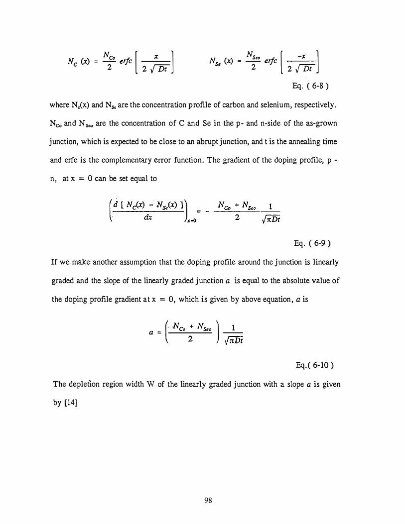
x N c (x) = N CJ erfc 2
[2 {Dt
] Se (x) = Ns�o erfc N[ -x
2 2 {75t l
Eq. ( 6-8 )
where Nc(x) and NSe are the concentration profile of carbon and selenium, respectively.
Nco and NSeo are the concentration of C and Se in the p- and n-side of the as-grown
j unction, which is expected to be close to an abrupt junction, and t is the annealing time
and erfc is the complementary error function. The gradient of the doping profile, p -
n , at x = 0 can be set equal to
Eq. ( 6-9 )
If we make another assumption that the doping profile around the j unction is linearly
graded and the slope of the linearly graded j unction a is equal to the absolute value of
the doping profile gradient at x = 0, which is given by above equation , a is
_ (- -NCo + N Seo 1 a -2
) --vrcDt
Eq. ( 6- 10 )
The depletion region width W of the linearly graded junction with a slope a is given
by [14]
98

Eq.( 6 - 1 1 ) where es is the dielectric constant, q is the electron charge and V bi is the built-in
potential . In our case,
W = [ W can be represented by
112e V 13 24Tibi ( l!2 e V 13 .r bi )1 6 ___ q ( s__ 1q
1= ( Dt ) 1
NCo + Sco ) ( NCo + N Seo )N 2 '{rcDt
Eq. ( 6-12 ) In Our Case e s - 12 · 0"' "'o• V bi - 1 • 9 V ' N Co = 1 X 10²⁰ 3cm· , N .,..., .. _ _ = 5 x 1019 cm·3 •
Dt = 1 x 10"16 X 30 x 60 cm2 = 1 . 8 X 1 0·13 cm2 for 30 mins. annealing time. With
these values , W - 1 14 A was estimated. In Figure 6.6 (a) JP at W = 1 14 A, the
estimated value of W of the tunnel junction annealed at 750 °C, is about an order of
magnitude less than JP at W = 95 A, which was the calculated value of W of the
assumed abrupt junction of the as-grown tunnel diode. Our rough estimate of the
decrease of the peak current density can partially explain the experimental results. Table
6 . 1 summarizes the main features of the tunnel diodes as-grown, annealed at 650 o c
an d 750 ° C . The results for the GaAs tunnel diode were also included for comparison.
6.4 Conclusion
A p+ -AlGaAs/n+ -GainP tunnel junction was grown by ALE using C and Se for
99

the p- and n-type dopants, respectively . There is only - 20 mV voltage drop across
this junction at 20 A/cm2, which is the expected current density for an AlGa.As/GaAs
t'W'O junction solar cell at 1000 suns operation. Our calculation shows that p+
AlGaAs/n+ -GainP heterostructure can be considered as a better material system than
p+ -AlGa.As/n+ -AlGaAs structure for the connecting tunnel diode in the cascade solar
structure, primarily because doping levels as high as 5 x 1 019 cm·3 can be achieved for
the n+ -side material. In addition, the conduction band discontinuity at the
heterointerface also contributes to high band-to-band tunnel current density. Even
though the performance of the tunnel diode annealed at temperatures higher than the
growth temperature, especially at 750 °C , showed degradations, probably due to the
diffusion of the dopant species, the voltage drop across the junction at 20 A/cm2 is still
low enough for this junction to be suitable for 1000 suns operation . This p+
A1GaAsfn+ -GainP heterostructure diode is the first .reported tunnel diode fabricated
using high band-gap material systems suitable for a cascade solar cell structure
operating at 1 000 suns.
1 00

References
[1] R.L. Moon, L.W. Janes , H.A. VanderPlas, Y. G . Chai , and G .A . Antypas,
Thirteenth IEEE Photovoltaic Special Conference , Washington ,D . C . ( IEEE,
New York, 1978 ) , p. 859,
[2] S .M. Bedair, M.F. Lamorte, and J.R. Hauser, Appl . Phys. Lett. 34, 3 8 (1979) .
[3] S .M. Bedair, J. Appl . Phys. 5 1 , 3935 (1980) .
[4] M. Konagai , T. Yamada, T. Akatsuka, K . Saito, E. Tok.'Umitsu , and K.
Takahashi , J . Cryst. Growth 98 , 167 (1989) .
[5] N. Kobayashi, T. Makimoto , and Y. Horikoshi , Appl. Phys. Lett. 50, 1435
(1987) .
[6] P.M. Mooney, J. Appl. Phys. 67, R1 (1990) .
[7] M.O. Watanabe and Y. Ohba, J . Appl. Phys. 60, 1032 ( 1986) .
[8] T. Ishikawa, T. Maeda, and K. Kondo, J . Appl. Phys . 68 , 3343 (1990) .
[9] J.R. Gong, D. Jung, N.A. El-Masry, and S .M. Bedair, Appl . Phys. :Lett. 57,
400 (1990) .
[10] K . G . Reid, H.M. Urdianyk, and S .M. Bedair, Appl . Phys. Lett. 59, 2397
(199 1).
[ 1 1] B .C. Chung, R.T. Green , and H.F. MacMillan, J . Cryst. Growth 107, 89
(199 1) .
[ 12] A. Usui and H. Sunakawa in lnst. Phys. Conf. Ser. no. 83, GaA.s and Related
Compounds, 129 ( 1986) .
[ 13] P. Basmaji , M. Guittard, A. Rudra, J .F . Carlin, and P. Gibart, J. Appl. Phys.
1 01

62 , 2 103 (1987) .
[14] S .M. Sze, Physics of Semiconductor Devices, 2nd Edition, New York: Wiley
( 1981) , Chap.9 .
[ 15] M.A. Rao, E.J . Caine, H. Kraemer, S .I . Long , and D.I. Babic, J. Appl. Phys.
61 , 643 (1987) .
[ 1 6] R.L. Anderson , Solid State Electron . 5, 34 1 (1962) .
[17] R.E. Hayes , P. Gibart, J. Chevrier, and S . Wagner, Solar Cells 15, 23 1 ( 1985) .
[ 1 8] G . A . DeJong, M.S. Thesis , North Carolina State University, Raleigh, N.C.
( 1978) .
[ 19] J . S . Blakemore, Semiconductor Statistics, (Dover, New York, 1987)
[20] H . C . Casey and M.B. Panish, Heterostructure Lasers, Part A and B, New
York, Academic Press (1978) .
[2 1] T. Kobayashi , K. Taira, F. Nakamura, and H. Kawai, J . Appl. Phys. 65, 4898
( 1989) .
[22] M . A. Haase, M.J. Hafich, and G . Y . Robinson, Appl. Phys. Lett. 58, 6 1 6
(1991) .
[23] B. Goldstein, Phys. Rev. 121 , 1305 ( 1961) .
[24] J . S . Kirkaldy and D.J . Young , Dif.!usion in The Condensed State , (The Institute
of Metals, London , U.K. 1987)
1 02

Table 6. 1 Main features of the heterojunction tunnel diodes as-grown , annealed at
650 oc and annealed at 750 oc. Results for a GaAs tunnel diode from Ref. [ l 3] were
also included for comparison .
1 03
Sample As-grown Annealed at Annealed at Ga.A.s
Peak Current
650°C 750° C
Density (A/cm2)
Peak Voltage
8 8 74 33 45
(mV) 140 270 240 136
Specific ·
Resistivity 1 .0 X 10-3 2 .9 X 10"3 4 .6 x 1 0-3 2.0 X 1 0"3
(Ocm2)
Voltage Drop at
- .
20 A/cm2 (mV) 2 1 58 100 37

2000 A Au
300 A NI 200 1-1m X 200 1-1m me sa
1 000 A AuGe
5000 A n GaAs
1 000 A n•GalnP
..,__ tunnel ju nction
1 000 A p• AIGaAs
./ \.. p GaAs substrate
2000 A Au
Figure 6. 1 Structure of the p+ -AlGaAs/n+ -GainP heterojunction tunnel diode.
1 04

1 00
80 -N \,:J E u 60 ......... < ........
>-·o; 40 c CD
0
·i: 200 ... ... :J u 0
-20 -0 .2 0 0 .2 0 .4 0 .6 0 .8
Voltage ( V )
Figure 6.2 J-V characteristics of the as-grown heterojunction tunnel diode at room
temperature and at 1 50 °K. The diode is oscillating in the negative differential
resistance region.
1 05

n-GalnP p-AIGaAs
Vacuum level - - - - -1'· - - - - -j[ · - - - - - - - - - - - - - - - - -if - -� - - - - - - - - - - - - - - - - - ·
Z1 X1
Efn - - - - - - - - - -'- - - - - - - - - - _..:::l_E_c ....... __ _, ____ Ec2
Ec1 __ _. ____________ � Z2 Eg2
Eg 1 .,....-----....,.,..._-..�--_ Ev2· · · - - - - - - - - - · - · - · · · · · · · - - - - - · Efp
Ev·1 ---------�---.J ..:::l Ev
A . Ec = X1 - X2
(a) Figure 6.3 Energy band diagram of isolated p+ -AlGaAs and n + -GainP (a) and the
expected band line-up when these two materials are brought together (b) .
106

Efn
Ec1
Ev1
n-GalnP
X1 Z1
Metallurgical junction
p-AJGaAs
Vacuum level
X2
Ec2
Z2
Eg2
Ev2 - - - - - _,_ - - - - - - - - - - - - � - - - - - - - - - - - - - - - - - - - - -Efp
Eg 1
I I .
�� · ... .... ,I I W1 W2
W = W1 + W2
(b)
1 07

I _!_ qV
T I
n-GalnP Metallurgical junction p-AIGaAs
,...-,..--------- Ec2 L1 Ec
t . . . . . . . Eg2 En
2
I 8
� . ) - - - - . -� . - - . . . . . . . . . -�- - -� ... ;/
. Integration level
Eln • · . . .
. -·· [ ! / l _ _ _ _ . . . . . Elp Ec1 ----.----,----,----- / -�. · . t-/
;J}t( , I
,:Jfl;>_·· , . �;;;] ._;,, . .
Ev1 --------------L---� . . (a)
r-- w -� Figure 6. 4 The band l ine-up of the p+-AIGaAsfn +-GalnP heterojunction at forward bias (a) and at reversebias {b) . The electron tunneling through the barrier is shown.
,_. 0 00

n-GalnP Metallurgical junction p-AIGaAs
Ec2
E2 Ep
Ll Ec
t . . . . : Ev2
I E1
v _!_ En� 8 ...,..·
· -------.. -� . - qV t. - - - . . . - -
T �� - - . . - - - - - - - - - - - - - - - - . . - - - ..
7
. . . . . � � - - - - : - - - - -:- - . - - - . . .
-
Integration level
Ee l
Eg1
(b) ' · ::
Ev 1
..... .
�-- w ·-1
....... 0 \0

25 i 20 (A)
1 5 (8) N E 0 CJ 1 0
-.....-................ 1 - - (C) <t 0 .... .,...
5 . , ' 0.5 w • .2:' ...... 0 �
· ... � ................ �--..
.,... (D) c II) 41 0 0 Q,l "C E -c E 41 -5 -0.5 ... ... ::1
(.) -1
- 1 .5
-2 0.00 0.05 0.1 0 0.1 5 0 .20 0 .25 0 .3 0
Voltage ( V )
(a)
Figure 6.5 The calculated J-V curves for four different tunnel diodes at room
temperature (a) and at 150 oK (b) . See text for the specification of diodes (A) , (B) , (C) ,
and (D) .
1 10

25 2.5
20 2 (A)
1 5 1 . 5 (B) C\1 E D ..g 1 0 1 - (C) <t 0 .... - I • � 5 0.5 w
!./" •• -------------· - 0
� .... (D) c:: � ell 0
------0 ell -c E - E c:: ·0.5ell ·5 ... ... ::::
(.) ·1
-1 5 ·1 .5
-20 . ·2 ·0.05 0.00 0.05 0.1 0 0.1 5 0.20 0.25 0.30
Voltage ( V )
(b)
1 1 1

1 000000�--------------------------------------�
1 00000
'"'E 1 00 0 0 u -<
1
0.1
0.01+---�--�--�--��-r--�--�--�--�--� 50 60 70 80 90 1 00 1 1 0 1 20 1 30 1 40 1 50
_ .Depletion layer thickness ( Angstrom )
(a)
Figure 6 .6 Variation of the peak tunnel current density JP with the depletion layer
thickness W (a) and W as a function of the doping level in the n-side of the p+-
AlGaAs/n+ -GainP heterojunction (b). In (b) , the doping level of the p+ -side of the
junction is fixed at 1 x 1 010 cm·3 •
1 12

Na = E 2 0 c m-3 E 400�--------------------------------------� 0 ... -� 350 c
<t Cl) Cl)
300
� 250 .:.! � '{3. 200
... Cll � 1 50 -1 c g 1 00Cll c. Cll 0 1 .00
Nd ( Times E1 9 cm-3 )
\ --JEc= 0.0 eV -- .t1Ec = 0.1 5 eV
(b)
1 0.00
1 13

1 0 0
8 0 .,....,. N
E u 6 0 ........ < '-'
>- 40 ;; c C) 0 c 2 0 C) '-'-
:I . . u
0
-20 -G.2 0 0.2 O A 0.6 0.8
Voltage ( V )
(a)
Figure 6.7 J-V characteristics of the samples annealed at 650 oc (a) and at 750 o c
(b) for 3 0 minutes. The measurements were performed at room temperature. The diodes
are oscillating
1 14

1 0 0
8 0,..... ('I E "' 6 0 < -£ 40., c: 0 0 c 2 0 0 ...... :::1 u
0
-2 0 -o.2 0 0 .2 0.4 0 .6 0.8 Voltage ( Y )
(b)
1
1 \
1 1 5

REPORT DOCUMENTATION PAGE Form Approved OMB NO. 0704-0188
Public reporting burden for this collection of information is estimated to average 1 hour per response, including the time for reviewin instructions, searching existing data sources, gathering and maintaining the data needed, and coml'leting � R collection of information, rncludi�suggestions for reduci'dl' and reviewing the collection of information. Send comments regardin t
this burden, to Washington Headquarters Services, Directorate for In o'('("is burden estimate or any other aspect of this ation Op)�tions and Relfcrts, 1 215 Jefferson
Davis Highway, Suite 1 204, Arlin on, , VA 22202-4302, an to the Office of Management and Butiget, Paperwork Reduction Project 0704-0188 3 , Washin!:lton, C 20503.
1 . AGENCY USE ONLY (Leave blank) 2. REPORT DATE 3. REPORT TYPE AND DATES COVERED December 1 997 Final Report
4. TITLE AND S U BTITLE 5. FUNDING N UMBERS
New Approaches for High-Efficiency Solar Cells; Final Report C: XDA-3-1 21 1 4-5 T A: PV802804
6. AUTHOR(S)
S.M. Bedair and N.A. EI-Masry
7. PERFORMING ORGAN IZATION NAME(S) AND ADDRESS(ES) 8. PERFORMING ORGANIZATION R EPORT NUMBER
North Carolina State University Raleigh, North Carolina 27695-791 1
9. SPONSORING/MON ITORING AGENCY NAME(S) AND ADDRESS(ES) 1 0 . SPONSORI NG/MONITORINGAGENCY REPORT NUMBER
National Renewable Energy Laboratory 1 6 1 7 Cole Blvd. SR-520-23266
Golden, CO 80401 -3393
1 1 . SU PPLEMENTARY NOTES
NREL Technical Monitor: R. McConnell
1 2a. DISTR I BUTION/AVAILABILITY STATEMENT 1 2b. DISTRIBUTION CODE
UC-1260
1 3. ABSTRACT (Maximum 200 words)
This report summarizes the activities carried out in this subcontract. These activities cover growing GaAs, AIGaAs, and lnGaP by atomic-layer epitaxy (ALE) at fairly low growth temperatures; using ALE to achieve high levels of doping both n-type and p-type required for tunnel junctions in the cascade solar cell structures; and studying the properties of AIGaAs/lnGaP and AIGaAs/GaAs tunnel junctions in stacked solar cell structures. The effect of these tunnel junctions on the performance of stacked solar cells was studied at different temperatures and different solar fluences. Researchers also studied the effect of different types of back-surface fields, both p/n and n/p GalnP solar cell structures, and their potential for window-layer applications. Parts of these activities were carried out in close cooperation with Dr. Mike Timmons of the Research Triangle Institute.
1 4. TERMS 1 5. NUMBER OF PAGES 121
photovoltaics ; high-efficiency solar cells ; atomic-layer epitaxy ; window-layer applications ; 1 6. PRICE CODE tunnel junctions ; back-surface fields
17. SECURITY CLASSIFICATION 18. SECURITY CLASSIFICATION 19. SECURITY CLASSIFICATION 20. LIMITATION OF ABSTRACT OF REPORT OF THIS PAGE OF ABSTRACT Unclassified Unclassified Unclassified UL
NSN 7540-01 -280-5500 Standard Form 298 (Rev. 2-89) Prescribed by ANSI Std. Z39-18
298-102