near infrared optical manipulation of a gaas/algaas …gervaislab.mcgill.ca/buset_msc_thesis.pdf ·...
TRANSCRIPT

Near Infrared Optical Manipulation of aGaAs/AlGaAs Quantum Well in the
Quantum Hall Regime
Jonathan M. Buset
Department of PhysicsMcGill University
Montreal, Quebec, CanadaAugust 2008
A thesis submitted to McGill Universityin partial fulfilment of the requirements of the degree of
Master of Science© Jonathan M. Buset, 2008

To my parents.
For always encouraging me to follow my dreams.
ii
Abstract
Using electronic spin rather than charge to replace existing microelectronic sys-
tems has been a well studied area of research in the last ten years. More recently,
research has focused on using the nuclear spin of GaAs rather than the electron spin.
This work has demonstrated that GaAs nuclear spins have many desirable properties
and show great potential as quantum information carriers. The challenge in the im-
plementation of nuclear spins lies in the ability to control and retrieve the information
that they carry. One proposed method is to dynamically polarize the GaAs nuclear
spins using circularly polarized photoexcitation. If successful, this could open new
horizons in the field of quantum information processing.
This thesis details an investigation into the use of polarized light to manipulate
the properties of a GaAs/AlGaAs quantum well sample. The three main topics ex-
plored in this thesis are: 1) the design and operation of a polarization controller that
is able to shine well-defined and tunable polarized light on to a sample contained
in a cryogenic environment at T = 0.27 K; 2) the manipulation of the nuclear po-
larization in GaAs using low power laser light with tunable polarization; and 3) a
preliminary investigation into illuminating a quantum Hall sample with unfocused,
low power laser light and the transport properties modifications that occur in the
quantum Hall regime.
iii

Resume
L’utilisation du spin electronique plutot que la charge electronique pour rem-
placer les systemes microelectroniques a ete un domaine bien etudie de la recherche au
cours des dix dernieres annees. Plus recemment, la recherche a porte sur l’utilisation
du spin nucleaire du GaAs plutot que le spin electronique. Ce travail a demontre
que les spins nucleaires du GaAs ont de nombreuses proprietes desirables et mon-
trent un grand potentiel en tant que transporteurs de l’information quantique. Le
defi dans la mise en œuvre des spins nucleaires reside dans la capacite de controler et
de recuperer les informations qu’elles transportent. Une methode proposee consiste a
polariser dynamiquement les spins nucleaires du GaAs en utilisant la photoexcitation
polarisee circulairement. Ceci pourrait ouvrir de nouveaux horizons dans le domaine
du traitement de l’information quantique.
Cette these expose en details une enquete sur l’utilisation de la lumiere polarisee
pour manipuler les proprietes d’un echantillon puit quantique de GaAs/AlGaAs. Les
trois principaux sujets abordes dans cette these sont les suivants: 1) la conception
et le fonctionnement d’un controleur de polarisation qui est capable d’emettre une
lumiere polarisee bien definie et ajustable sur un echantillon dans un environnement
cryogenique a T = 0.27 K, 2) la manipulation de la polarisation nucleaire dans le
GaAs en utilisant un laser a faible puissance avec une polarisation ajustable, et 3)
une enquete preliminaire sur l’illumination d’un echantillon de Hall quantique avec
iv

un laser non-focalise a faible puissance et les modifications des proprietes de transport
qui se produisent dans le regime de Hall quantique.
v

Acknowledgements
The research group that I worked in was full of fun and friendly peers, all of
whom I now consider to be my friends. My heartfelt thanks go out to all of the past
and present members of the Gervais Group. Immeasurable thanks go to Cory Dean
and Dr. Benjamin Piot for their guidance, encouragement and support throughout
the many days and long nights we spent together in the lab; to Andrew Mack for your
endless enthusiasm and tireless work spent building and testing the optics system; to
Dominique Laroche for preparing our sample and teaching me to use the cryogenic
system; to Michel Savard for sharing our cramped corner of the basement; to James
Hedberg for making the lab an amazingly fun place to work in; to Vera Sazonova
for your amazing Labview skills; and to my supervisor Dr. Guillaume Gervais for
providing the equipment and helium necessary to help run all of my experiments.
Many people around the Rutherford building have directly contributed to my
research and I would like to acknowledge their contributions here. Thanks go out
to John Smeros for ensuring that the liquid helium was always plentiful; to Richard
Talbot for helping to build the apparatus and ensuring that everything stayed in
working order; to Dr. Paul Wiseman for enlightening conversations on the Fara-
day rotation model; and to Dr. Thomas Szkopek for conversations regarding the
phenomena discussed in Chapter 4.
vi

I also wish to thank all of my friends in the Department of Physics for mak-
ing these past two years fun and enjoyable. Many thanks go to Philip Egberts for
sharing a cube with me and keeping me entertained throughout the long days; to
Dylan McGuire and Jody Swift for keeping me fed and well caffeinated throughout
this entire process; to Adam Schneider for always being around to have a chat with;
to Etienne Marcotte for being my go-to guy for everything Matlab, to Jeff Bates and
Jessica Topple for being amazing neighbours; and to the rest of my friends in the de-
partment: Tobin Filleter, Jesse Maassen, Chris Voyer, Rene Breton, Aleks Labuda,
Dan O’Donnell, Kevin MacDermid, James Kennedy, Vance Morrison, Robert Chate-
lain, and Ashley Faloon. Sincere apologies to anyone that I may have forgotten.
Throughout many of the long days and nights spent completing this work, I
have been supported by my wonderful girlfriend Jessica. Her patience and kindness
during this process has been above and beyond the call of duty.
Finally, I wish to thank my family for always supporting me in whatever (mis)-
adventures I get myself into. Immeasurable thanks go to my parents Richard and
Liz; to my grandparents; to my sister Kathleen; and to all of my extended family.
This whole process would not have been possible without your love and support.
vii

Table of Contents
Abstract . . . . . . . . . . . . . . . . . . . . . . . . . . . . . . . . . . . . . . . iii
Resume . . . . . . . . . . . . . . . . . . . . . . . . . . . . . . . . . . . . . . . iv
Acknowledgements . . . . . . . . . . . . . . . . . . . . . . . . . . . . . . . . . vi
List of Figures . . . . . . . . . . . . . . . . . . . . . . . . . . . . . . . . . . . x
List of Abbreviations . . . . . . . . . . . . . . . . . . . . . . . . . . . . . . . . xvi
1 Introduction . . . . . . . . . . . . . . . . . . . . . . . . . . . . . . . . . . 1
1.1 Motivation . . . . . . . . . . . . . . . . . . . . . . . . . . . . . . . 11.1.1 GaAs/AlGaAs Quantum Wells . . . . . . . . . . . . . . . . 31.1.2 Classical Hall Effect . . . . . . . . . . . . . . . . . . . . . . 41.1.3 Integer Quantum Hall Effect . . . . . . . . . . . . . . . . . 71.1.4 Resistively Detected Nuclear Magnetic Resonance . . . . . 101.1.5 Light-Matter Interactions and Optical Pumping . . . . . . 131.1.6 Double Resonance & Dynamic Nuclear Polarization . . . . 14
1.2 Thesis Objectives & Organization . . . . . . . . . . . . . . . . . . 26
2 Polarization Controller . . . . . . . . . . . . . . . . . . . . . . . . . . . . 27
2.1 Controller Operation . . . . . . . . . . . . . . . . . . . . . . . . . 272.2 Simulation Without A Magnetic Field . . . . . . . . . . . . . . . . 302.3 Magnetic Field Effects . . . . . . . . . . . . . . . . . . . . . . . . 322.4 Conclusions . . . . . . . . . . . . . . . . . . . . . . . . . . . . . . 37
3 Magneto-optical Quantum Transport Measurements . . . . . . . . . . . . 38
3.1 Experiment . . . . . . . . . . . . . . . . . . . . . . . . . . . . . . 383.1.1 Apparatus . . . . . . . . . . . . . . . . . . . . . . . . . . . 383.1.2 Optics Calibration . . . . . . . . . . . . . . . . . . . . . . . 39
viii

3.1.3 GaAs/AlGaAs Quantum Well . . . . . . . . . . . . . . . . 423.2 Polarization Dependence Sweeps . . . . . . . . . . . . . . . . . . . 463.3 2D Maps of Resistance and Polarization . . . . . . . . . . . . . . . 493.4 Dynamics Experiments . . . . . . . . . . . . . . . . . . . . . . . . 503.5 Conclusions . . . . . . . . . . . . . . . . . . . . . . . . . . . . . . 53
4 Laser Induced Phenomena in GaAs/AlGaAs Quatum Wells . . . . . . . . 55
4.1 Zero Resistance States Under Laser Illumination . . . . . . . . . . 554.2 Contact Dependence . . . . . . . . . . . . . . . . . . . . . . . . . 564.3 Temperature Dependence . . . . . . . . . . . . . . . . . . . . . . . 594.4 Laser Power Dependence . . . . . . . . . . . . . . . . . . . . . . . 66
4.4.1 Reduced Laser Power . . . . . . . . . . . . . . . . . . . . . 664.4.2 No Illumination . . . . . . . . . . . . . . . . . . . . . . . . 674.4.3 Increased Laser Power . . . . . . . . . . . . . . . . . . . . . 684.4.4 Electron Density . . . . . . . . . . . . . . . . . . . . . . . . 69
4.5 Conclusions . . . . . . . . . . . . . . . . . . . . . . . . . . . . . . 71
5 Conclusions . . . . . . . . . . . . . . . . . . . . . . . . . . . . . . . . . . 72
5.1 Summary . . . . . . . . . . . . . . . . . . . . . . . . . . . . . . . 725.2 Future Research . . . . . . . . . . . . . . . . . . . . . . . . . . . . 73
5.2.1 Nuclear Magnetic Resonance . . . . . . . . . . . . . . . . . 735.2.2 Polarization Controller . . . . . . . . . . . . . . . . . . . . 745.2.3 Laser Induced Phenomena . . . . . . . . . . . . . . . . . . 75
A Further Details . . . . . . . . . . . . . . . . . . . . . . . . . . . . . . . . 76
A.1 Contact Quality Circuit . . . . . . . . . . . . . . . . . . . . . . . 76A.2 Sample Growth Data . . . . . . . . . . . . . . . . . . . . . . . . . 77
B Software Source Code . . . . . . . . . . . . . . . . . . . . . . . . . . . . 78
B.1 Experimental Analysis of α− β Maps . . . . . . . . . . . . . . . . 78B.2 Simulation of α− β Maps and Faraday Rotation . . . . . . . . . . 79B.3 Analysis of B Field Sweeps . . . . . . . . . . . . . . . . . . . . . . 80
References . . . . . . . . . . . . . . . . . . . . . . . . . . . . . . . . . . . . . . 87
ix

List of Figures
Figure page
1–1 Example energy band diagram for a GaAs/AlGaAs heterojunction inthermal equilibrium. A mismatch of the conduction and valenceband energies (Ec and Ev) of the two materials creates a potentialbarrier at the junction interface. . . . . . . . . . . . . . . . . . . . . 4
1–2 Triangular potential well formed by a GaAs/AlGaAs heterojunction.The resulting 2-DEG has quantized energy levels in the z -direction. 5
1–3 Illustration of the geometry used to measure the Hall effect in a n-typesemiconductor. . . . . . . . . . . . . . . . . . . . . . . . . . . . . . 6
1–4 Example of a typical magnetotransport measurement (Rxx and Rxy
vs. B) demonstrating the quantum Hall effect in a GaAs/AlGaAs2DEG at T ≈ 270 mK. The labelled arrows denote the Landaulevel filling factors ν at certain magnetic fields. . . . . . . . . . . . 8
1–5 Density of states in a 2DEG in a strong perpendicular magnetic field.(a) An ideal 2D crystal with no disorder broadening. (b) A realistic2D crystal where the shaded regions represent the localized statesthat form in the tails of each Landau level as a result of the disorderdue to defects and impurities. . . . . . . . . . . . . . . . . . . . . . 9
1–6 Illustration of a typical NMR experiment where the sample is placedin a uniform external magnetic field B and the in-plane magneticfield (perpendicular to B) created by the coil is B1. . . . . . . . . . 10
1–7 (a) When placed in an external magnetic field, the magnetic momentof the nuclei will precess with frequency νL. (b) Energy leveldiagram for spin 1
2nucleus. When the spin is aligned with the
magnetic field, it resides in its lowest energy state E1 and in thehigher energy state E2 when the spin is oriented opposite to thefield. . . . . . . . . . . . . . . . . . . . . . . . . . . . . . . . . . . 11
x

1–8 (a) A photon with energy E = hν > Eg is absorbed by a conductionband electron. (b) The electron is elevated into the valence band,creating an electron-hole pair. . . . . . . . . . . . . . . . . . . . . . 14
1–9 Energy level diagram for the allowed transitions of a simple systemwith S = 1
2and I = 1
2in an applied magnetic field B0. Each state
is denoted in a simplified form where, for example, |+−〉 representsmS = +1
2, mI = −1
2. γn is assumed to be negative in this figure. . . 16
1–10 Energy band diagram for the Overhauser effect. Wij representthe thermally induced transitions that try to maintain thermalequilibrium. Electron spin transitions are shown in blue andcombined nucleus-electron spin flips are shown in red. An appliedalternating field induces spin transitions at a rate We shown in green. 18
1–11 Energy level diagrams describing the use of forbidden transitionswhich flip both the electron and nucleus simultaneously to producenuclear polarization. The transitions Wen illustrated in (a) and (b)will produce nuclear polarization of opposite signs. In this model itis assumed that transitions involving and electron spin-flip are theonly significant thermal processes. . . . . . . . . . . . . . . . . . . . 20
1–12 Illustration of the optical Overhauser effect in a simple four statesystem under photoexcitation by (a) right handed and (b) lefthanded circularly polarized light. . . . . . . . . . . . . . . . . . . . 25
2–1 Illustration of the polarization controller apparatus. The red pathshows the forward propagating light and the blue denotes the pathof the back-reflected light. All of the optical components are atroom temperature while the light is transmitted onto a sample atT ≈ 270 mK. . . . . . . . . . . . . . . . . . . . . . . . . . . . . . . 29
2–2 Contour maps of the back-reflection intensity at zero magnetic field asa function of waveplate angles α and β. (a) Typical experimentaldata taken at low temperature, T ≈ 270 mK. (b) Jones matrixsimulation using Eq. 2.4 and Eq. 2.5 with fitting parametersφ = 1.3π, ψ = 0.64π and θ = 1.26π for the optical fiber. . . . . . . 32
xi

2–3 Magnetic field gradient along the z-axis inside the cryostat wherez = 0 corresponds to the centre of the superconducting magnet. Theshaded region denotes the area of the field where the optical fiber ispresent starting at z = 0.019 m. The box shows the approximationof a uniform magnetic field B over a length l = 0.12 m. The areaenclosed by the rectangle is equal to the area under the curve inthe field profile. . . . . . . . . . . . . . . . . . . . . . . . . . . . . . 35
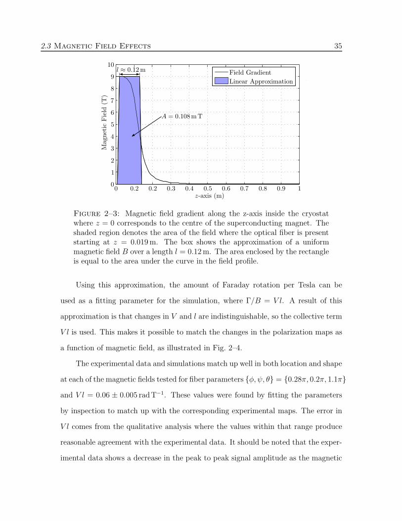
2–4 Contour maps showing the polarization controller output in differentmagnetic fields. (a) Maps of experimental data (T ≈ 270 mK) and(b) the corresponding Jones matrix simulations. As the magneticfield is increased, the regions of circularly polarized light begin torotate counterclockwise and become distorted. . . . . . . . . . . . . 36
3–1 Illustration of the cryogenic environment in the Janis HE-3-SSVsystem. The inset on the left demonstrates how the optical fiber(shown in red) is fixed above the sample surface. The verticalmagnetic field gradient provided by Janis is shown along the lengthof the cryostat. This helps demonstrate that the loop of fiberattached to the charcoal sorb is out of the B field. . . . . . . . . . 40
3–2 The configuration used for aligning the optics. The fiber is passedthrough the guide and aligned with the photosensor inside thepower detector. . . . . . . . . . . . . . . . . . . . . . . . . . . . . . 41
3–3 Example of a typical power calibration curve for the output of theoptical fiber with a sharp turn-on current of ID ≈ 43 mA. . . . . . . 41
3–4 Room temperature α − β maps of (a) back-reflection and (b) trans-mission intensity. In certain map regions, there is a fluctuation inpower of approximately 8%. . . . . . . . . . . . . . . . . . . . . . . 42
3–5 Calculation of the approximate band structure of sample accordingto the growth recipe. Note that the region from 425 nm − 500 nmmay not be completely flat. This error is due to improper boundaryconditions in the software used to generate the band structure. Webelieve the structure has some curvature demonstrated as dashedlines in the figure. . . . . . . . . . . . . . . . . . . . . . . . . . . . 43
xii

3–6 (a) Approximate configuration of the ohmic contacts located onsample. The red gradient represents the beamspot of the unfocusedlight emanating from the end of the fiber showing its approximatecoverage of the sample. (b) Standard measurement geometry fora quantum transport experiments conducted. Ix represents thesourcing current, Rxx the magnetoresistance and Rxy the Hallresistance. . . . . . . . . . . . . . . . . . . . . . . . . . . . . . . . . 44
3–7 (a) Trace of the magnetoresistance as a function of magnetic fieldbefore and after the sample was illuminated by the LED. Exposingthe sample to 225µAs (2 × 1.5µA for 75 s) was usually enough tobring the ν = 1 quantum Hall state within the range of the system’smagnet. (b) Density returns to near that of the dark state afterthe sample is warmed to T ≈ 40 K. Both traces were taken at basetemperature T ≈ 270 mK. . . . . . . . . . . . . . . . . . . . . . . . 46
3–8 (a) ν = 1 quantum Hall state of the 2DEG. The red circle highlightsthe approximate location of the optical transport measurements.(b) A contour map of back-reflection intensity measuring the outputpolarization at B = 5.6 T. . . . . . . . . . . . . . . . . . . . . . . . 47
3–9 Changes in magnetoresistance versus light polarization of a GaAs/AlGaAs2DEG at T ≈ 270 mK, B = 6.77 T and the base Rxx = 450 Ω. Asmall phase offset is found in the back-reflection signal with respectto the resistance oscillations, which is attributed to the additionalFaraday rotation that the back-reflected light undergoes in compar-ison to the light illuminating the sample, as discussed in Chapter 2. 48
3–10 Two α−β maps of (a) back-reflection and (b) ∆Rxx/Rxx. The regionslabelled σ and σ′ represent transmission of a different handednessof circularly polarized light. T ≈ 270 mK, B = 6.770 T, P ≈ 72µWpower output from the fiber . . . . . . . . . . . . . . . . . . . . . . 50
3–11 (a) α − β map of back-reflection at B = 7.1561 T. (b) A measure-ment of the magnetoresistance decay as the polarization of lightilluminated on the sample was changed from σ to || at t = 0 s. . . . 51
3–12 Decay of magnetoresistance near ν = 1 as the polarization of lightshining on the sample is changed at t = 0 s from (a) || → σ and (b)σ → ||. . . . . . . . . . . . . . . . . . . . . . . . . . . . . . . . . . 52
3–13 Decay curve of magnetoresistance with a time constant of τ1 =380 ± 110 s as the polarization is changed from σ′ → || at t = 0 s. . 53
xiii
4–1 Transport sweeps of Rxx and Rxy with B (a) increasing and (b)decreasing. The dashed red line is a linear fit to the Hall resistancefor B < 2 T and extrapolated to show the change in curvature ofRxy at higher magnetic fields. . . . . . . . . . . . . . . . . . . . . . 56
4–2 Comparison of transport measurements taken using different contactconfigurations on the GaAs/AlGaAs sample. The only differencebetween (a) and (b) is that the source current is moved from thecentre of the sample to the left side. In (c) the left side of thesample is probed showing only a single density. . . . . . . . . . . . 58
4–3 Illustration of the band structure modifications that result fromphotoexcitation with energy below that of the bandgap. In theilluminated region, the build up of charge raises the potential atthe GaAs/AlGaAs interface which acts like a depleting back gatebias and reduces the local electron density in the 2DEG. . . . . . . 59
4–4 Magnetic field sweeps (a) up (b) down showing the temperaturedependence of a GaAs/AlGaAs quantum well under constantillumination from near infrared laser light. A clear change in theelectron density of the quantum well is evident by the shift of theRxx valleys as the temperature increases. The step-like nature inthe plots is due to the interpolation method used to generate thecontour. . . . . . . . . . . . . . . . . . . . . . . . . . . . . . . . . . 61
4–5 Demonstration of the temperature dependence of the quantum well’selectron density. The solid lines are fits to the Boltzmann approxi-mation in Eq. 4.1 with the given fitting parameters. . . . . . . . . . 63
4–6 The offset in Rxx and Rxy is still present at higher temperatures.Only even number filling factors are present as the states due tospin splitting have closed at T = 2.2 K. . . . . . . . . . . . . . . . . 64
4–7 B field sweeps (a) up and (b) down of the magnetoresistance’s tem-perature dependence. The data in has been adjusted to compensatefor changes in the well’s electron density. . . . . . . . . . . . . . . . 65
4–8 Temperature dependence of the peak height of the structures (γ andδ) on either side of the crossing over gap. In (a) δ shows a slowdecline with temperature, whereas in (b) γ demonstrates a sharpturn behaviour at T = 0.7 K. . . . . . . . . . . . . . . . . . . . . . 66
xiv

4–9 Transport measurements acquired as the illumination power wasdecreased. As the power was lowered, the structures of the unknownzero resistance states begins to degrade. At low power, the curvatureof the Hall resistance has subsided. . . . . . . . . . . . . . . . . . . 67
4–10 Measurements of the sample’s transport properties with no laserillumination. One can compare the state of the sample (a) beforeand (b) after it was allowed to warm to T ≈ 5 K. The sampleshows a very poor quality trace before the thermal cycle. After thesample was warmed, it appears to have had a complete recoveryand all of the zero resistance states correspond to plateaus in theHall resistance. . . . . . . . . . . . . . . . . . . . . . . . . . . . . . 68
4–11 Demonstration of the effect that illumination power has on thequantum Hall system. At higher power, the zero resistance statesbegin to degrade as the electron heating becomes significant. Unlikethe high temperature data in Fig. 4–6, even at high power there isstill considerable curvature in the Hall resistance at high magneticfields. . . . . . . . . . . . . . . . . . . . . . . . . . . . . . . . . . . 69
4–12 Electron density as a function of illumination power shining onto thesurface of the GaAs/AlGaAs sample. Due to constraints beyondcontrol, the data was acquired in the following order: (1) Laserpower decreased. (2) Laser turned off. (3) Thermal cycle toT ≈ 5 K. (4) Laser turned on. (5) Power increased to 100µW.After step (4) the data clearly follows the same trend as (1),suggesting the effect of the laser is well mastered. . . . . . . . . . . 70
5–1 Illustration of a Hall bar sample with a width of 100µm. The contactarms, shown in blue, are patterned using standard photolithographytechniques. . . . . . . . . . . . . . . . . . . . . . . . . . . . . . . . 75
A–1 Diagram of the circuit used to test the quality of the sample contacts. 76
A–2 Molecular beam epitaxy growth data sheet for the wafer EA0746.The GaAs/AlGaAs quantum well sample used for all experimentsdescribed in this thesis was from this wafer. . . . . . . . . . . . . . 77
xv

List of Abbreviations
2DEG . . . . . . . . . . . Two-Dimensional Electron Gas
DNP . . . . . . . . . . . . Dynamic Nuclear Polarization
FQHE . . . . . . . . . . Fractional Quantum Hall Effect
IQHE . . . . . . . . . . . Integer Quantum Hall Effect
LED . . . . . . . . . . . . Light Emitting Diode
MBE . . . . . . . . . . . . Molecular Beam Epitaxy
MOSFET . . . . . . . Metal-Oxide Semiconductor Field Effect Transistor
NMR . . . . . . . . . . . Nuclear Magnetic Resonance
NPC . . . . . . . . . . . . Negative Photoconductivity
NPPC . . . . . . . . . . Negative Persistent Photoconductivity
OPNMR . . . . . . . Optically Pumped Nuclear Magnetic Resonance
PPPC . . . . . . . . . . Positive Persistent Photoconductivity
RDNMR . . . . . . . Resistively Detected Nuclear Magnetic Resonance
RF . . . . . . . . . . . . . . Radio Frequency
SOP . . . . . . . . . . . . State of Polarization
xvi

CHAPTER 1
Introduction
1.1 Motivation
Technological advancements in crystal growth, lithography and de-
velopment processes over the last 30 years have allowed for great strides in the
development of semiconductor devices. The most prevalent of these was the devel-
opment of Silicon Metal-Oxide Semiconductor Field Effect Transistors (MOSFETs)
which has revolutionized the technology industry worldwide. As these technologies
have advanced and the feature sizes have reached the nanometer scale, the number
of devices present on each integrated circuit has followed Moore’s law, approximately
doubling each year. As we begin to reach the limits of current fabrication techniques,
new research has started to focus on the development of nanostructured devices that
use an electron’s spin rather than its charge for modern device applications [1].
The behaviour of these new “spintronic” devices is primarily dictated by the
quantum mechanical interaction of electron charge and spin which show potential for
the realization of an architecture for quantum information processing. This work is
primarily motivated by the greater degree of freedom provided by spins and also their
higher level of isolation from the environment which makes the quantum mechanical
1

1.1 Motivation 2
states less prone to decoherence [2]. In comparison to electronic spin, the nuclear
spins of GaAs offer even greater isolation from the environment and show great
potential as quantum information carriers if one can find a way to effectively initialize,
control and read out their quantum mechanical states [3].
An important property of GaAs is the relatively strong hyperfine coupling that
exists between the electron and the nuclear spin degrees of freedom which recently
enabled the local study of multiple coherence of the nuclear spins by resistive meth-
ods [4]. These properties, in addition to the long nuclear spin coherence time (≈ ms),
make GaAs an appealing candidate for the implementation of quantum electronic
devices based on hyperfine-coupled nuclear spins.
One potential route toward the addressing and efficient manipulation of the
GaAs nuclear spins is through dynamic nuclear polarization and the optical Over-
hauser effect [5–7] where light in the near infrared spectrum with a well-defined
circular polarization is used to create a large out-of-equilibrium nuclear spin polar-
ization. Pumping nuclear spins via the optical Overhauser effect is more efficient
with circular polarized illumination than with linear polarized light [8, 9]. The abil-
ity to control the polarization of the light in situ at the active device region offers,
in principle, a means to manipulate the polarization of a small ensemble of nuclear
spins.
This thesis presents an investigation into the the use of polarized light to ma-
nipulate the nuclear spins of GaAs along with an analysis of the custom built polar-
ization controller used throughout the course of this research. In the remainder of
this chapter, references will be made to several key areas of research which motivated
this work.
1.1 Motivation 3
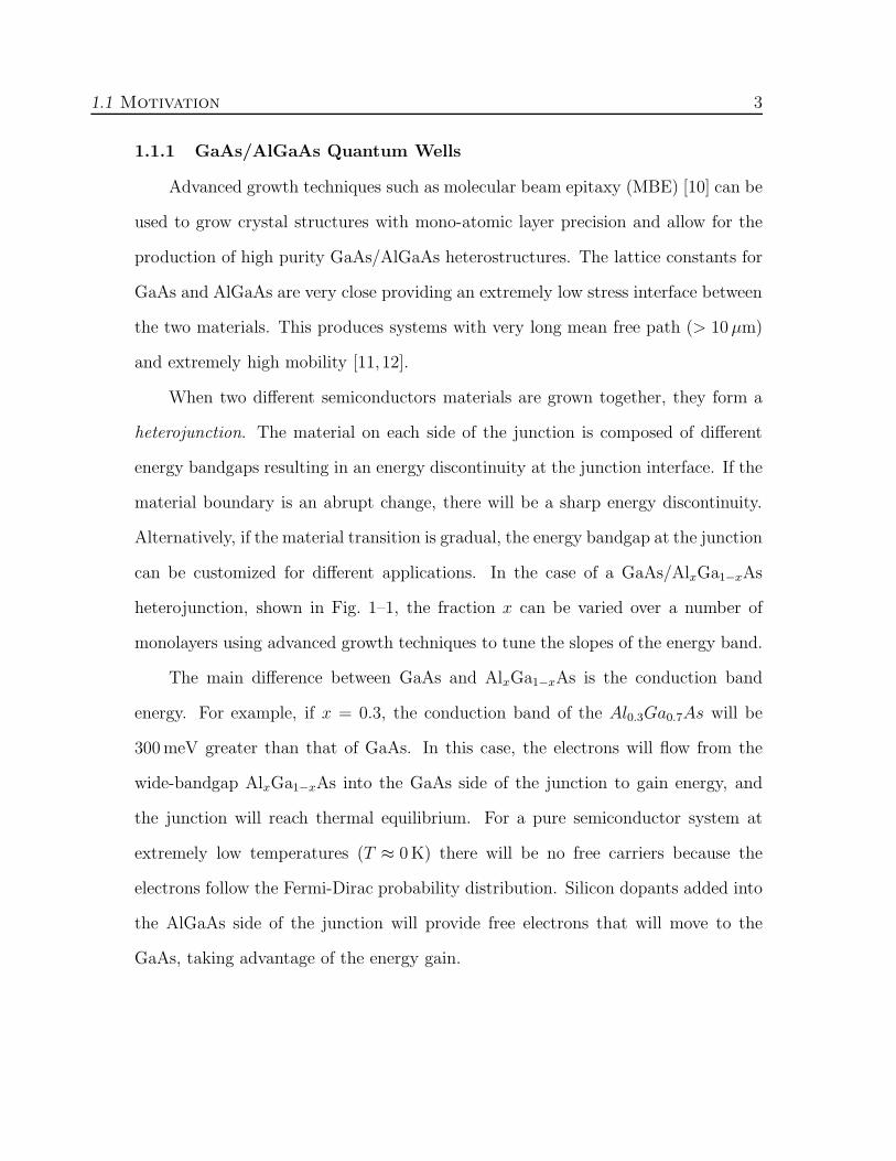
1.1.1 GaAs/AlGaAs Quantum Wells
Advanced growth techniques such as molecular beam epitaxy (MBE) [10] can be
used to grow crystal structures with mono-atomic layer precision and allow for the
production of high purity GaAs/AlGaAs heterostructures. The lattice constants for
GaAs and AlGaAs are very close providing an extremely low stress interface between
the two materials. This produces systems with very long mean free path (> 10µm)
and extremely high mobility [11, 12].
When two different semiconductors materials are grown together, they form a
heterojunction. The material on each side of the junction is composed of different
energy bandgaps resulting in an energy discontinuity at the junction interface. If the
material boundary is an abrupt change, there will be a sharp energy discontinuity.
Alternatively, if the material transition is gradual, the energy bandgap at the junction
can be customized for different applications. In the case of a GaAs/AlxGa1−xAs
heterojunction, shown in Fig. 1–1, the fraction x can be varied over a number of
monolayers using advanced growth techniques to tune the slopes of the energy band.
The main difference between GaAs and AlxGa1−xAs is the conduction band
energy. For example, if x = 0.3, the conduction band of the Al0.3Ga0.7As will be
300 meV greater than that of GaAs. In this case, the electrons will flow from the
wide-bandgap AlxGa1−xAs into the GaAs side of the junction to gain energy, and
the junction will reach thermal equilibrium. For a pure semiconductor system at
extremely low temperatures (T ≈ 0 K) there will be no free carriers because the
electrons follow the Fermi-Dirac probability distribution. Silicon dopants added into
the AlGaAs side of the junction will provide free electrons that will move to the
GaAs, taking advantage of the energy gain.
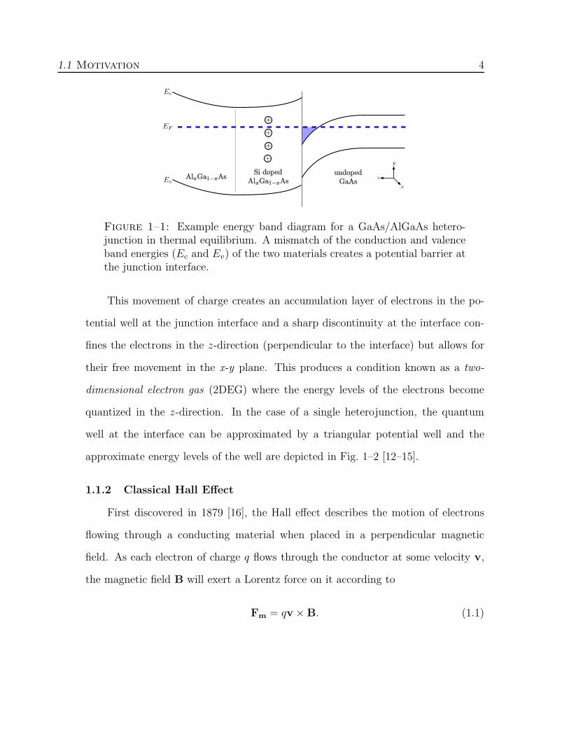
1.1 Motivation 4
Figure 1–1: Example energy band diagram for a GaAs/AlGaAs hetero-junction in thermal equilibrium. A mismatch of the conduction and valenceband energies (Ec and Ev) of the two materials creates a potential barrier atthe junction interface.
This movement of charge creates an accumulation layer of electrons in the po-
tential well at the junction interface and a sharp discontinuity at the interface con-
fines the electrons in the z-direction (perpendicular to the interface) but allows for
their free movement in the x-y plane. This produces a condition known as a two-
dimensional electron gas (2DEG) where the energy levels of the electrons become
quantized in the z -direction. In the case of a single heterojunction, the quantum
well at the interface can be approximated by a triangular potential well and the
approximate energy levels of the well are depicted in Fig. 1–2 [12–15].
1.1.2 Classical Hall Effect
First discovered in 1879 [16], the Hall effect describes the motion of electrons
flowing through a conducting material when placed in a perpendicular magnetic
field. As each electron of charge q flows through the conductor at some velocity v,
the magnetic field B will exert a Lorentz force on it according to
Fm = qv × B. (1.1)

1.1 Motivation 5
Figure 1–2: Triangular potential well formed by a GaAs/AlGaAs hetero-junction. The resulting 2-DEG has quantized energy levels in the z -direction.
Fig. 1–3 illustrates the Hall effect in a n-type semiconductor in a uniform mag-
netic field B = zBz with current Ix flowing in the x-direction. The electrons (or holes
for p-type semiconductors) flowing through the semiconductor will undergo a force
in the negative y-direction due to Eq. 1.1. The force on the carriers creates a net
buildup of charge carriers on the y = 0 surface of the semiconductor. This buildup
generates a transverse electric field in the y-direction which continues to increase
until the induced field is strong enough to stop the drift of the charge carriers. Once
a steady state is reached, the Lorentz force from the magnetic field will be exactly
balanced by the force of the induced electric field and the net force on the charge
carriers is zero.
F = q [E + (v × B)] = 0 (1.2a)
which leads to
qEy = qvxBz. (1.2b)

1.1 Motivation 6
Figure 1–3: Illustration of the geometry used to measure the Hall effect ina n-type semiconductor.
The electric field induced in the y-direction EH is known as the Hall field which
produces a potential difference across the width of the semiconductor known as the
Hall voltage. The Hall voltage in a conductor of width W is given by
VH = +EHW. (1.3)
For metals and n-type semiconductors where electrons are the majority carrier,
the induced Hall field will be in the negative y-direction and the resulting Hall
voltage will be negative with the given geometry of Fig. 1–3. For the same geometry
of p-type semiconductors, the induced field will be in the opposite direction and
the Hall voltage will be positive. As a result, the majority carrier of an extrinsic
semiconductor can be determined (either n-type or p-type) by measuring the polarity
of the Hall voltage.

1.1 Motivation 7
Combining Eq. 1.2 and Eq. 1.3, and substituting the drift velocity for electrons
in a n-type semiconductor,
vx =−Jxen
=−Ix
(en) (Wd)(1.4)
results in a Hall voltage given by
VH = −IxBz
ned. (1.5)
Rearranging Eq. 1.5 forms a ratio known as the Hall resistance (also called the Hall
coefficient).
RH =VHIx
= − Bz
ned(1.6)
The Hall resistance which is linear with B, proves to be a very useful tool in deter-
mining the electron density of the conducting sample [13–15,17].
1.1.3 Integer Quantum Hall Effect
A very interesting phenomenon occurs when the Hall effect is observed in two
dimensional systems held at low temperatures. When a magnetic field is applied
perpendicular to the conduction plane, the in-plane motion of the carriers becomes
quantized into Landau levels with energies given by
Ei =
(
i+1
2
)
~ωc, (1.7)
where ωc = eBm∗ is the cyclotron frequency, B is the magnetic field, e is the charge of
an electron and m∗ is its effective mass. The number of available states per cm2 in
each Landau level,
d =2eB
h, (1.8)

1.1 Motivation 8
is linearly proportional to the magnetic field. At low temperatures, the Landau levels
are split in two according to electron spins with each level having a degeneracy of
eBh
. In this case, the electron distribution in the 2DEG is given by the Landau level
filling factor
ν =n
d= n
(
h
eB
)
. (1.9)
A typical transport measurement demonstrating the quantized Hall effect is
shown in Fig. 1–4. As first discovered by von Klitzing, the trace exhibits the distinct
plateaus in the Hall resistance and corresponding minima in magnetoresistance when
the Landau level filling factor reaches integer values [18].
ν = n
(
h
eBi
)
= i (1.10)
Figure 1–4: Example of a typical magnetotransport measurement (Rxx
and Rxy vs. B) demonstrating the quantum Hall effect in a GaAs/AlGaAs2DEG at T ≈ 270 mK. The labelled arrows denote the Landau level fillingfactors ν at certain magnetic fields.
1.1 Motivation 9
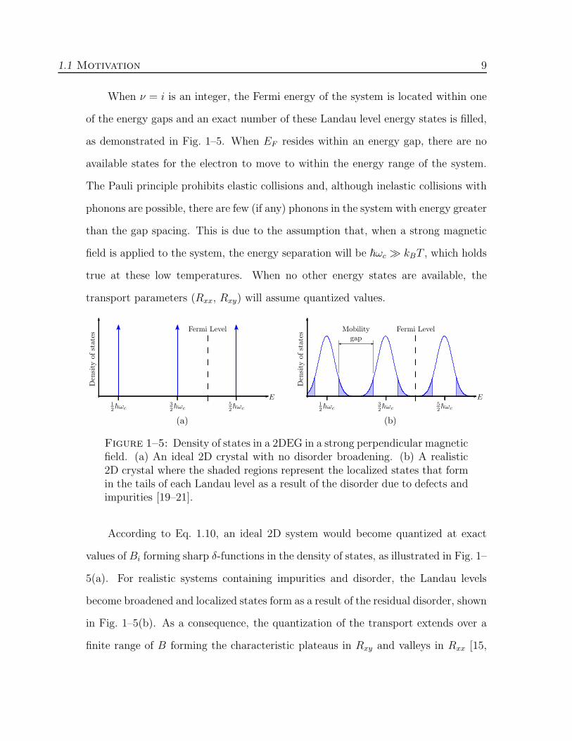
When ν = i is an integer, the Fermi energy of the system is located within one
of the energy gaps and an exact number of these Landau level energy states is filled,
as demonstrated in Fig. 1–5. When EF resides within an energy gap, there are no
available states for the electron to move to within the energy range of the system.
The Pauli principle prohibits elastic collisions and, although inelastic collisions with
phonons are possible, there are few (if any) phonons in the system with energy greater
than the gap spacing. This is due to the assumption that, when a strong magnetic
field is applied to the system, the energy separation will be ~ωc ≫ kBT , which holds
true at these low temperatures. When no other energy states are available, the
transport parameters (Rxx, Rxy) will assume quantized values.
(a) (b)
Figure 1–5: Density of states in a 2DEG in a strong perpendicular magneticfield. (a) An ideal 2D crystal with no disorder broadening. (b) A realistic2D crystal where the shaded regions represent the localized states that formin the tails of each Landau level as a result of the disorder due to defects andimpurities [19–21].
According to Eq. 1.10, an ideal 2D system would become quantized at exact
values of Bi forming sharp δ-functions in the density of states, as illustrated in Fig. 1–
5(a). For realistic systems containing impurities and disorder, the Landau levels
become broadened and localized states form as a result of the residual disorder, shown
in Fig. 1–5(b). As a consequence, the quantization of the transport extends over a
finite range of B forming the characteristic plateaus in Rxy and valleys in Rxx [15,

1.1 Motivation 10
19–21]. The description presented here focuses exclusively on the Integer Quantum
Hall Effect (IQHE) which is the regime of most importance to the investigations in
this thesis. There also exists systems that exhibit quantization when the Landau
level filling factor equals rational fraction values, known as the Fractional Quantum
Hall Effect (FQHE), as can be observed at ν = 53
in Fig. 1–4 [20–22].
1.1.4 Resistively Detected Nuclear Magnetic Resonance
Since its discovery by Bloch [23] and Purcell [24] in the 1940s, nuclear magnetic
resonance (NMR) has grown to become a powerful scientific tool with many appli-
cations including spectroscopy and medical imaging. In essence, nuclear magnetic
resonance is a technique used to observe the transition of nuclei between two spin
states. Fig. 1–6 shows an example of a typical NMR experiment, where a sample is
placed into a uniform d.c. magnetic field. A coil attached to a radio-frequency oscil-
lator is also wrapped around the sample providing a relatively weak second magnetic
field B1 oriented perpendicular to B.
Figure 1–6: Illustration of a typical NMR experiment where the sampleis placed in a uniform external magnetic field B and the in-plane magneticfield (perpendicular to B) created by the coil is B1..
When the sample is exposed to an external magnetic field, the nuclear magnetic
moments µ of the nuclei will precess at the Larmor precessional frequency
νL = γnB, (1.11)

1.1 Motivation 11
where γn is the gyromagnetic ratio of the nuclei and B is the magnetic field.
The potential of a nuclear magnetic dipole in an external magnetic field is E =
−µ · B, which is at its minimum when projection of the magnetic dipole is aligned
with B and maximum when oriented opposite to B. Fig. 1–7(b) demonstrates an
example energy level diagram for a spin 12
system.
(a) (b)
Figure 1–7: (a) When placed in an external magnetic field, the magneticmoment of the nuclei will precess with frequency νL. (b) Energy level diagramfor spin 1
2nucleus. When the spin is aligned with the magnetic field, it resides
in its lowest energy state E1 and in the higher energy state E2 when the spinis oriented opposite to the field.
When the frequency of the oscillator driving the coil reaches the Larmor fre-
quency, a torque will be generated on the precessing magnetic moments causing
them to transition between two spin states. The spin state transitions cause energy
to be absorbed by the system which can be detected inductively by an antenna.
Since it probes the bulk of the sample, the major limitation of classical NMR is
when the number of nuclei becomes too small for detection. Using modern techniques,
the minimum number of spins required for detection is approximately 1016. For
systems with smaller scales such as quantum dots (106−1010 spins), carbon nanotubes

1.1 Motivation 12
(< 103 spins per tube) and GaAs/AlGaAs 2DEGs (< 1015 spins for a 30 nm well),
the number of spins is too low to be detected using traditional NMR methods.
A number of techniques have been developed to increase the detection resolu-
tion in systems with small number of spins, including optically pumped NMR (OP-
NMR) [25, 26], magnetic resonance force microscopy [27], and resistively detected
NMR (RDNMR) [28]. RDNMR, which was first discovered by von Klitzing’s group
in 1988, has become a powerful tool in studying quantum Hall systems by utilizing
the coupling between the electrons and nuclei that is a result of the strong hyperfine
interaction, AI · S, in a GaAs/AlGaAs heterostructure [29, 30].
In an external magnetic field B = Bz, the total electronic Zeeman energy can
be written as
Ez = g∗µBBSz + A 〈Iz〉Sz (1.12)
where g∗ is the effective electronic g factor, Sz is the electron spin parallel to the
magnetic field, A is the hyperfine coupling constant, and 〈Iz〉 is the nuclear spin
polarization. The Zeeman energy in Eq. 1.12 can be rewritten as
Ez = g∗µB (B +BN )Sz (1.13)
where the finite nuclear polarization creates an effective magnetic field known as the
Overhauser shift BN = A 〈Iz〉 /g∗µB. In quantum Hall systems, the magnetoresis-
tance in the thermally activated region near the zero resistance states,
Rxx ∝ e−∆/2kBT , (1.14)
is a function of the energy gap ∆ which, in turn, is dependent on the Zeeman energy.
This relation demonstrates that Rxx is in fact sensitive to changes is nuclear spin
since its value is determined to some extent by the hyperfine coupling.

1.1 Motivation 13
In GaAs, the induced effective magnetic field BN will be in opposition to the
external magnetic field since the effective g factor is negative (g∗ = −0.44), which
will lower the total Zeeman energy in Eq. 1.13. Depolarizing the nuclear spins in
the sample by applying transverse radio frequency (RF) radiation at the isotope’s
NMR resonance will increase the Zeeman gap as BN → 0. In quantum Hall systems
at odd Landau level filling factors (i.e. ν = 1) the gap energy ∆ varies directly
with the Zeeman gap. Therefore, a change in the nuclear polarization will result
in a measurable change in Rxx providing the detection mechanism for the nuclear
magnetic resonance [31, 32].
1.1.5 Light-Matter Interactions and Optical Pumping
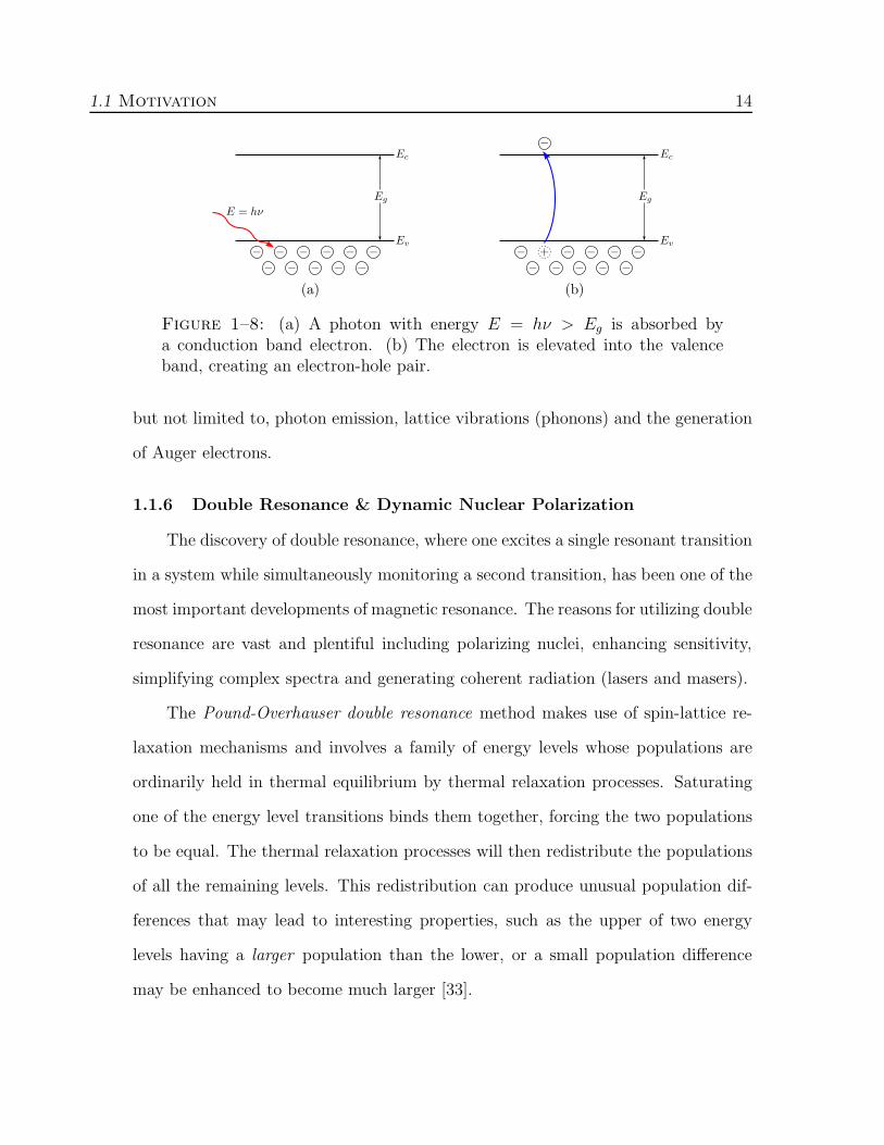
In semiconductors, there are a number of possible pathways for photon interac-
tion to occur. Photons can interact with the crystal lattice and convert their energy
into heat by interacting with impurity atoms or with defects in the semiconductor
crystal. The most important interaction is that between a photon and valence band
electron, as depicted in Fig. 1–8, where the photon has energy E = hν = hcλ
and the
semiconductor’s bandgap energy is Eg = Ec − Ev.
If the photon has energy E = hν < Eg it will be unable to elevate the valence
electrons to the conduction band. The semiconductor will be transparent to photons
in this energy range and they will not be absorbed. If hν > Eg, the photon has
enough energy to interact with a valence band electron and provides enough energy
to elevate it into the conduction band leaving a hole in the valence band. This
process is known as electron-hole pair generation.
After the electron is elevated to a higher energy level, the system will eventually
return to thermal-equilibrium and the electron will recombine with the hole in the
conduction band to release the excess energy through numerous pathways including,
1.1 Motivation 14
(a) (b)
Figure 1–8: (a) A photon with energy E = hν > Eg is absorbed bya conduction band electron. (b) The electron is elevated into the valenceband, creating an electron-hole pair.
but not limited to, photon emission, lattice vibrations (phonons) and the generation
of Auger electrons.
1.1.6 Double Resonance & Dynamic Nuclear Polarization
The discovery of double resonance, where one excites a single resonant transition
in a system while simultaneously monitoring a second transition, has been one of the
most important developments of magnetic resonance. The reasons for utilizing double
resonance are vast and plentiful including polarizing nuclei, enhancing sensitivity,
simplifying complex spectra and generating coherent radiation (lasers and masers).
The Pound-Overhauser double resonance method makes use of spin-lattice re-
laxation mechanisms and involves a family of energy levels whose populations are
ordinarily held in thermal equilibrium by thermal relaxation processes. Saturating
one of the energy level transitions binds them together, forcing the two populations
to be equal. The thermal relaxation processes will then redistribute the populations
of all the remaining levels. This redistribution can produce unusual population dif-
ferences that may lead to interesting properties, such as the upper of two energy
levels having a larger population than the lower, or a small population difference
may be enhanced to become much larger [33].
1.1 Motivation 15
This effect was first theorized by Overhauser [34] who predicted that, if one
saturated the conduction electron spin resonance in a metal, the nuclear spins would
be polarized 1000 times more strongly than their normal polarization in the absence
of electron saturation. The first double resonance experiment was conducted by
Pound on the 23Na nuclear resonance of NaNO3 where a 53
factor enhancement of
the +12
to −12
transition was seen after he saturated the 32
to 12
transition [35]. The
second double resonance experiment was conducted by Carver who was the first to
demonstrate dynamic nuclear polarization and to validate Overhauser’s revolutionary
prediction [5].
A Model System
As an example, one can look at the energy levels of a simple system with nuclear
spin I = 12
that is coupled to an electron of spin S = 12, and acted on by an external
magnetic field B0. The system can be described by the Hamiltonian
H = γe~B0Sz + AI · S− γn~B0Iz (1.15)
where the subscripts e and n denote electrons and nuclei. This model assumes in the
strong field approximation that γe~B0 ≫ A. The result is that Sz nearly commutes
with H so its eigenvalue mS can be considered a good quantum number. Since now
only AIzSz has diagonal terms, the effective Hamiltonian is
H = γe~B0Sz + AIzSz − γn~B0Iz (1.16)
If we take the quantum number of Iz (mI) as another good quantum number, the
energy eigenvalues of the system will be
E = γe~B0mS + AmImS − γn~B0mI (1.17)
1.1 Motivation 16
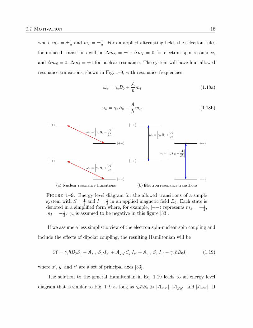
where mS = ±12
and mI = ±12. For an applied alternating field, the selection rules
for induced transitions will be ∆mS = ±1, ∆mI = 0 for electron spin resonance,
and ∆mS = 0, ∆mI = ±1 for nuclear resonance. The system will have four allowed
resonance transitions, shown in Fig. 1–9, with resonance frequencies
ωe = γeB0 +A
~mI (1.18a)
ωn = γnB0 −A
~mS. (1.18b)
(a) Nuclear resonance transitions (b) Electron resonance transitions
Figure 1–9: Energy level diagram for the allowed transitions of a simplesystem with S = 1
2and I = 1
2in an applied magnetic field B0. Each state is
denoted in a simplified form where, for example, |+−〉 represents mS = +12,
mI = −12. γn is assumed to be negative in this figure [33].
If we assume a less simplistic view of the electron spin-nuclear spin coupling and
include the effects of dipolar coupling, the resulting Hamiltonian will be
H = γe~B0Sz + Ax′x′Sx′Ix′ + Ay′y′Sy′Iy′ + Az′z′Sz′Iz′ − γn~B0In (1.19)
where x′, y′ and z′ are a set of principal axes [33].
The solution to the general Hamiltonian in Eq. 1.19 leads to an energy level
diagram that is similar to Fig. 1–9 as long as γe~B0 ≫ |Ax′x′ |, |Ay′y′ | and |Az′z′|. If

1.1 Motivation 17
these assumptions are true, then mS is still a good quantum number, but mI may
not be. In this case, the lowest order wave functions ψi will no longer be
ψi = |mSmI〉 , (1.20)
but rather a linear combination of such states
ψi =∑
mS ,mI
cimSmI|mSmI〉 . (1.21)
The result of using the more general Hamiltonian in Eq. 1.19 over that in Eq. 1.15 is
that through the application of an alternating field, resonance transitions other than
those shown in Fig. 1–9 become possible. These additional transitions are known by
convention as forbidden transitions [8, 9, 33, 36].
The Overhauser Effect
Although Overhauser’s original prediction was focused on the polarization of
nuclei in a metal, one can use the simplified model presented in the previous section
to illustrate the process he proposed. This example assumes that the principal relax-
ation mechanisms are electron spin relaxations (W12,W21,W34,W43) and a combined
nuclear-electron spin flip (W23,W32) as demonstrated in Fig. 1–10.
An alternating field is applied to induce transitions between the ψ1 and ψ2 states
at a rateWe, whereWe corresponds to an electron spin resonance. In this case, we will
define pi as the probability of occupying the state ψi. A series of differential equations
results, (full details provided by Slichter [33]), and the steady state solution results

1.1 Motivation 18
Figure 1–10: Energy band diagram for the Overhauser effect. Wij rep-resent the thermally induced transitions that try to maintain thermal equi-librium. Electron spin transitions are shown in blue and combined nucleus-electron spin flips are shown in red. An applied alternating field induces spintransitions at a rate We shown in green [33].
are found to be
p1 = p2 (1.22)
p3 = p4W43
W34
(1.23)
p3 = p2W23
W32
(1.24)
where Eq. 1.22 is the due to the clamped populations, and Eq. 1.23 and Eq. 1.24 are
the normal thermal equilibrium population ratios for the pairs of states (ψ3, ψ4) and
(ψ2, ψ3) respectively.
Since the pairs (p3, p4) and (p2, p3) are in thermal equilibrium, the ratio of p4 to
p2 must also be in thermal equilibrium. For a pair of levels in thermal equilibrium,
they can be defined by the Boltzmann ratio Bij where
pj = pie(Ei−Ej)/kBT
≡ piBij (1.25)

1.1 Motivation 19
This leads us to rewrite the probabilities as
p1 = p2 =1
2 +B23 +B24
(1.26)
p3 =B23
2 +B23 +B24
(1.27)
p4 =B24
2 +B23 +B24
, (1.28)
which gives an average nuclear spin polarization of
〈Iz〉 =∑
i
pi 〈i| Iz |i〉
=1
2(p1 + p2 − p3 − p4)
=1
2
2 − B23 −B24
2 +B23 +B24. (1.29)
To look at the significance of this expression, one can look at the high temperature
limit where Bij∼= 1 +
Ei−Ej
kBT, which results in
〈Iz〉 =1
2
γe~B0 +(
A
2
)
+ 2γn~B0
4kBT
∼= 1
2
γe~B0
4kBT(1.30)
If the sample was not being saturated by an external field, the expectation value of
the nuclear spin in thermal equilibrium would be
〈Iz〉therm =1
2
γn~B0
2kBT. (1.31)
Comparing Eq. 1.30 and Eq. 1.31, we find that by saturating the electron spin reso-
nance We the mean nuclear spin has increased by
〈Iz〉〈Iz〉therm
=γe2γn
. (1.32)
1.1 Motivation 20
In the case of a metal, as originally proposed by Overhauser, each electron
couples to a number of nuclei so there is only a single electron resonance. This would
be equivalent to saturating both electron resonances in our model, so the resulting
mean nuclear spin polarization is
〈Iz〉〈Iz〉therm
=γeγn. (1.33)
as originally predicted by Overhauser [8, 9, 33, 36].
Polarization by Forbidden Transitions
It was Abragam [37] and Jeffries [38] who independently recognized that these
forbidden transitions were not strictly forbidden, and in some circumstances they
could be used to a great advantage in achieving nuclear polarization. The two possible
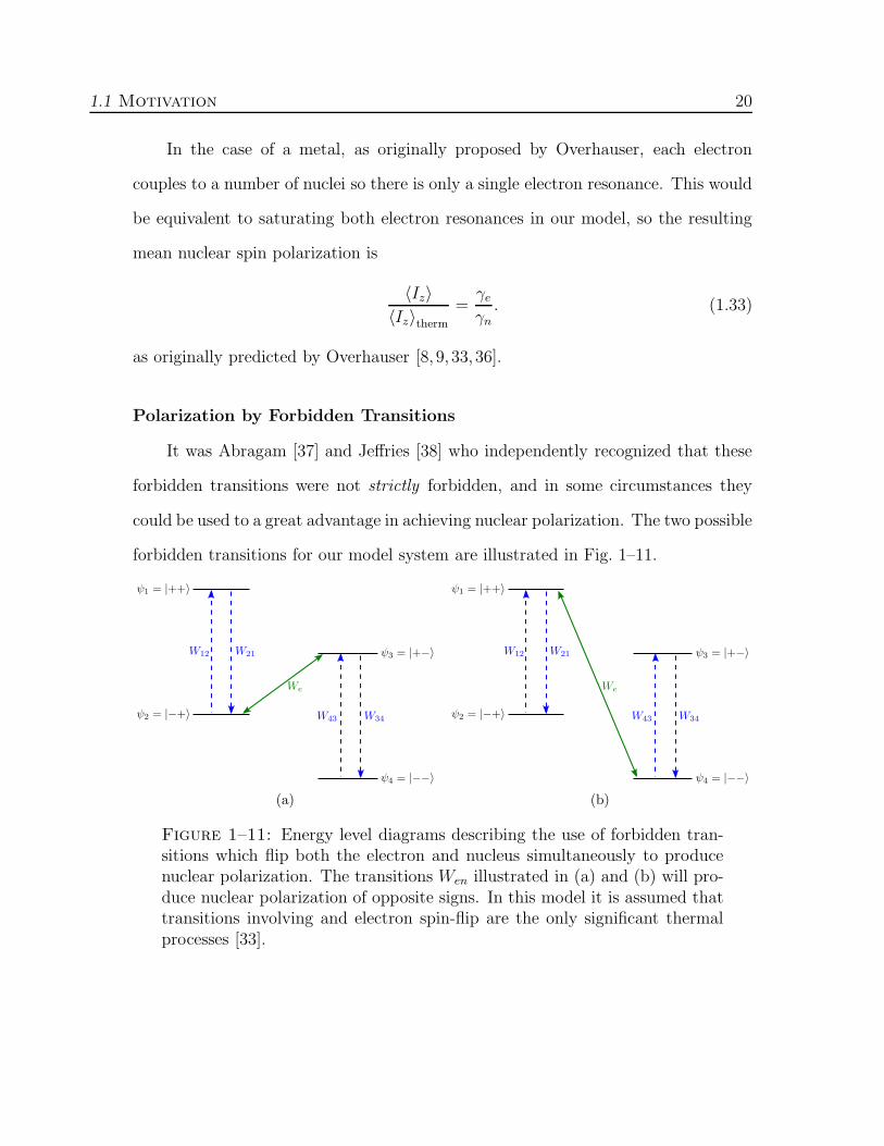
forbidden transitions for our model system are illustrated in Fig. 1–11.
(a) (b)
Figure 1–11: Energy level diagrams describing the use of forbidden tran-sitions which flip both the electron and nucleus simultaneously to producenuclear polarization. The transitions Wen illustrated in (a) and (b) will pro-duce nuclear polarization of opposite signs. In this model it is assumed thattransitions involving and electron spin-flip are the only significant thermalprocesses [33].

1.1 Motivation 21
The transitions in Fig. 1–11 can be induced by alternating fields perpendicular
to B0 when the general Hamiltonian in Eq. 1.19 is solved to adequate precision.
Although the transition probability Wen is often small, it can produce effective pop-
ulation equalization if Wen is made larger than the thermal transition rate at which
a nucleus flips. To further illustrate this point, we will analyze the saturation of the
forbidden transition illustrated in Fig. 1–11(b).
Assuming that the only possible thermal transitions are those shown in the
figure, we can immediately see that
p1 = p4 (1.34a)
p2 = p1e(E1−E2)/kBT = p1B12 (1.34b)
p3 = p4e(E4−E3)/kBT = p4B43 (1.34c)
and can therefore see that
p1 = p4 =1
2 +B12 +B43(1.35a)
p2 =B12
2 +B12 +B43(1.35b)
p3 =B43
2 +B12 +B43. (1.35c)
The average expectation value of nuclear spin Iz is given by
〈Iz〉 =∑
i
pi 〈i| Iz |i〉
=1
2(p1 + p2 − p3 − p4)
=1
2
B12 −B34
2 +B12 +B43(1.36)

1.1 Motivation 22
To look at the significance of this expression, we once again can look at the mean
nuclear spin polarization in the high temperature limit
〈Iz〉 =1
2
γe~B0
2kBT. (1.37)
This leads to an enhancement over the normal polarization of
〈Iz〉〈Iz〉therm
=γeγn
(1.38)
which is once again the result originally predicted by Overhauser [8, 9, 33, 34, 36].
Dynamic Nuclear Polarization through Optical Methods
The first example of this dynamic nuclear polarization (DNP) by photoelectrons
was observed in 29Si by Lampel who found that, under excitation in circularly polar-
ized light, the NMR signal was much larger than what was observed without optical
pumping [39]. The mechanism of the strong influence of the excitation light polar-
ization on the nuclear spins has been well studied [40]. The effect of polarization
at nuclear resonance is due to the change of the hyperfine magnetic field BN (see
Eq. 1.13) experienced by the photoelectrons as a result of the dynamically polarized
nuclei. A comprehensive review of this effect is presented by Paget and Burkovitz [9].
In order to determine the dependence of the nuclear spin polarization on the
handedness of the polarized light, one must first look at the interactions of the
photons and the electron spin system. The degree of circular polarization P of the
luminescence light can be defined as
P =L+ − L−
L+ + L−, (1.39)
1.1 Motivation 23
where L± is the intensity of the σ±-polarized component of the total luminescence [9,
41]. Here we define σ+ and σ− respectively as right and left handed circularly
polarized light.
Under optical pumping conditions, the same selection rules describe the ab-
sorption of a circularly polarized photon and the radiative recombination of a spin-
polarized electron. As a result, we find that the mean electronic spin is related to
the degree of circular polarization by
〈S〉 = −P. (1.40)
In these systems the interaction between a single electron of spin S and a nucleus
of spin I is described by the Fermi contact Hamiltonian HF [8]. Since this Hamilto-
nian is of the form AI · S = A[
12(I+S− + I−S+) + IzSz
]
, the nuclei are dynamically
polarized allowing for the simultaneous reversal of a nuclear spin and an electronic
spin. The value of the mean nuclear spin is then
〈I〉 =I (I + 1)
S (S + 1)[〈S〉 − 〈ST 〉] , (1.41)
where I and S are the nuclear and electronic spins respectively, 〈S〉 is the optical
pumping mean electronic spin and 〈ST 〉 is the electronic mean spin in the exter-
nal magnetic field. This equation holds true for 〈I〉 ≪ 1 and, in most cases, the
thermodynamic mean 〈ST 〉 is negligible compared to 〈S〉 and 〈I〉 is simply propor-
tional to 〈S〉 [9]. Therefore, we find the resulting relationship between luminescence
polarization and nuclear spin polarization to be
〈I〉 ∝ −P. (1.42)

1.1 Motivation 24
It has also been shown that only localized electrons (see Fig. 1–5) are efficient
at dynamically polarizing nuclear spins [9]. These localized electrons are found in
all practical cases, and can be trapped on shallow donors [42] or in the spatial
fluctuations within the conduction band minima of doped semiconductors [41]. This
is significant for these studies, as experiments were conducted on the flank of ν = 1
in the region of the localized states.
A Qualitative Illustration
This complex relationship can be clarified in a simple illustrative argument using
conservation of spin angular momentum and the model described in the previous
section. Here an attempt will be made to qualitatively describe the interaction of
the circularly polarized photons with the system. Although presented for a two level
system, this model should also hold true for systems with spins I > 12
and S > 12.
First, it should be noted that the spin angular momentum of a circularly polar-
ized photon is −~ for σ+ and +~ for σ−. One of the finer points of detail is that we
cannot define a spin for linearly polarized light but rather, since all the photons are
identical, each will have an equal probability of being in an −~ or +~ state. There-
fore, there will be no overall angular momentum imparted by a linearly polarized
beam of light. In the case of elliptically polarized light, there is an unequal proba-
bility of each being in either spin state so a net angular moment will be imparted to
the target [43].
In Fig. 1–12, an example four state system is used, but in this case the system
is under excitation by circularly polarized photons. In Fig. 1–12(a) a σ+ photon
interacts with the mS = +12
due to conservation of spin angular momentum, and the
photoexcited electron’s spin flips to become mS = −12. This will create an excess
of electrons in states ψ2 = |−+〉 and ψ4 = |−−〉. This population increase in ψ2

1.1 Motivation 25
and ψ4 will cause a redistribution of the other state’s populations. Specifically, the
excess electrons in ψ2 can relax through the hyperfine pathway W23 and repopulate
ψ3. This will result is an overall 〈Iz〉 > 0. We note that rather than a full saturation
of the transition as described previously for the Overhauser effect, it is suggested
that a steady state population inversion will result from the photoexcitation.
For the opposite case in Fig. 1–12(b), one sees that the σ− photons interact
with the mS = −12
increasing the populations of ψ1 and ψ3 through conservation
of spin momentum. Here the hyperfine relaxation pathway W32 will restore some
of the population to ψ2. The populations in (ψ3, ψ4) will be greater than (ψ1, ψ2),
producing in an overall 〈Iz〉 < 0.
(a) (b)
Figure 1–12: Illustration of the optical Overhauser effect in a simple fourstate system under photoexcitation by (a) right handed and (b) left handedcircularly polarized light.
Although Paget’s mechanism presented here for the dynamic nuclear polariza-
tion in GaAs has been well studied in the literature, it should be noted that con-
tradictory results have been found. In the work by Barrett, results following this
relationship as found in Eq. 1.42 were not observed. It was noted that this may
have been the result of the the high magnetic fields in their experiments affecting
the selection rules, equilibrium polarization of electrons and holes, or the relaxation

1.2 Thesis Objectives & Organization 26
processes which can affect the resulting nuclear polarization [25]. This observation
hints that, under certain conditions, the dynamic nuclear polarization process may
not be as straightforward as previously thought.
1.2 Thesis Objectives & Organization
The main objectives of this thesis is to experimentally investigate the effect of
illuminating a GaAs/AlGaAs quantum well in the integer quantum Hall regime with
different polarizations of near infrared laser light. Each chapter of this thesis will
focus on a different set of experiments performed on the system.
Chapter 2 will present the design and implementation of the polarization con-
troller system used to illuminate the sample during the transport measurements. A
numerical model will be presented along with supporting experimental data. In addi-
tion, the complications that arise when the controller is used in a system containing
a superconducting magnet are explored.
In Chapter 3 the results of magneto-optical transport measurements performed
using the polarization controller and a single GaAs/AlGaAs quantum well sample are
discussed. The dependence of the ν = 1 quantum Hall state on the polarization of the
light used for excitation was investigated using resistively detected NMR techniques.
In addition, dynamics experiments were conducted to determine the relaxation rate
of the system under different polarizations of light.
Chapter 4 presents an examination of different phenomena found to occur in
a quantum Hall system under photoexcitation by low power infrared laser light.
A thorough investigation of these phenomena’s dependence on contact geometry,
temperature and laser power is presented.

CHAPTER 2
Polarization Controller
The ability to actively control the polarization of light is a vital neces-
sity to utilize dynamic nuclear polarization to manipulate nuclear spins. In
this chapter we introduce the design and operation of a polarization controller for
laser-light in the near infrared spectrum with an optical fiber held at low tempera-
tures where all of the optical components are kept outside of the cryogenic system.
A complete analysis of the polarization controller is presented in the case where the
optical fiber is enclosed inside a large magnet, and it is shown that the scheme can be
used to produce well-defined light polarizations even in the presence of a relatively
strong magnetic field.
2.1 Controller Operation
The polarization controller presented builds upon the work of Heismann et al.
and consists of three birefringent waveplates, two λ/4 separated by one λ/2 [44],
as depicted in Fig. 2–1. This combination of waveplates is capable of transmitting
any arbitrary state of polarization (SOP) into the optical fiber by simply varying
the waveplate angles [44]. The polarization axes of the two λ/4 waveplates in the
apparatus are separated by 90° with respect to each other. The angles α and β
27
2.1 Controller Operation 28
represent the amount of clockwise rotation of the slow axis from the vertical for each
of the λ/4 and λ/2 waveplates respectively. These waveplate angles were initialized
with a computer camera to an accuracy of 0.2°. The controller uses a 5 mW near
infrared diode laser of wavelength λ ≈ 800 nm along with a single-mode optical fiber
(SM800, 125µm cladding diameter) to transmit the polarized light onto a sample
mounted inside of a commercial 3He cryostat (Janis HE-3-SSV) containing a 9 T
superconducting magnet. In order to deflect the back-reflected signal of the light
entering the fiber, the injector end was cleaved at an angle of ∼ 8°. Neglecting
losses, it is assumed that the optical fiber acts as a birefringent transformation on
the light [45], and as such, the backward propagating light undergoes the inverse
polarization change as the light propagating in the forward direction. Therefore, the
birefringent fiber and waveplates are known as reciprocal media [46]. There exists
a natural birefringence of the optical fiber which is primarily due to mechanical
deformation such as twisting and stress inside the fiber [47]. These properties may
vary with each experiment so each time the cryostat is placed in the Dewar the fiber
at room temperature is fixed in place for the remainder of the experiment.
The novelty of the polarization controller presented is based on the isolation and
measurement of the small amount of light reflected back from the interface at the
end of the fiber. In order to provide information about the light exiting the fiber,
the back-reflected signal is isolated using a polarizing cube beam splitter located
between the laser source and the first waveplate. The purpose of the cube is twofold,
it first acts as a vertical polarizer for the source laser light before it interacts with
the retarding waveplates. Secondly, it acts as a horizontal polarization filter and a
45° mirror for the back-reflected light.
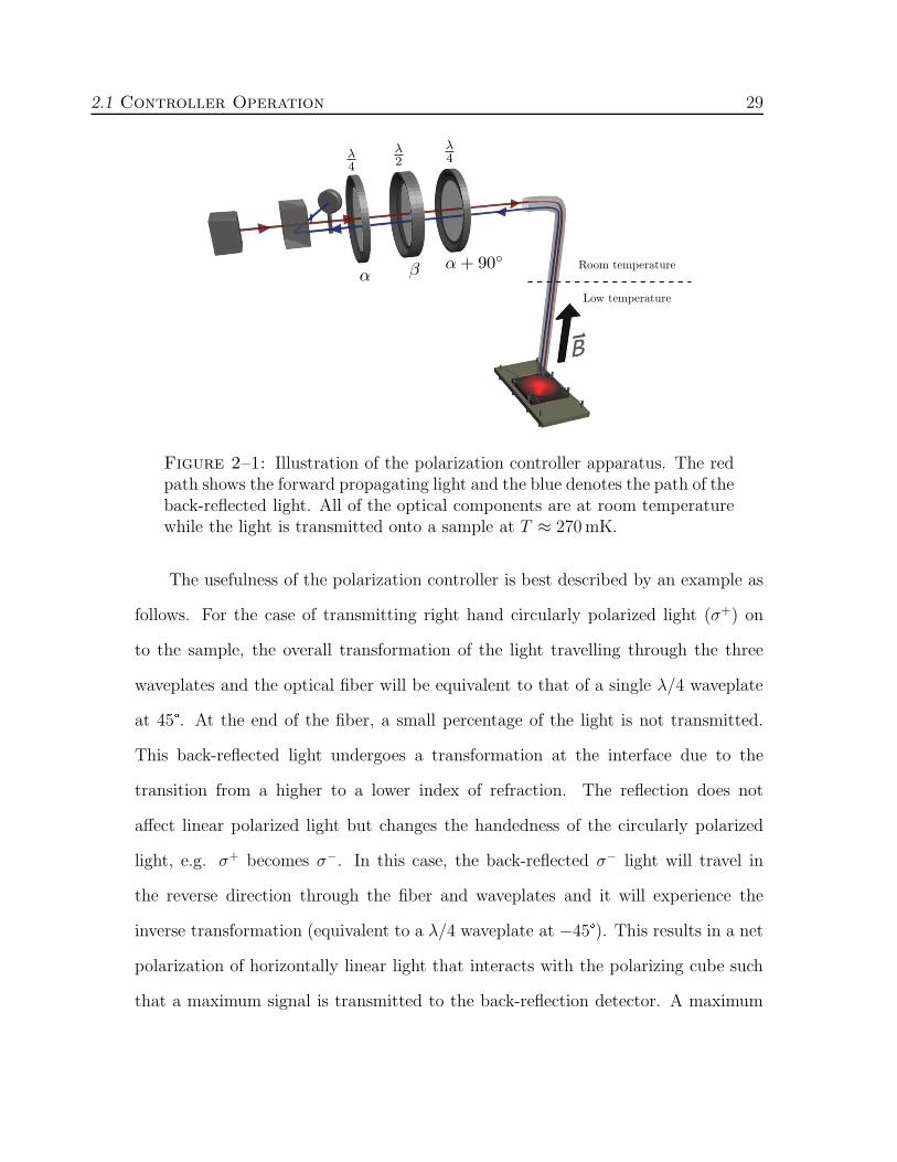
2.1 Controller Operation 29
Figure 2–1: Illustration of the polarization controller apparatus. The redpath shows the forward propagating light and the blue denotes the path of theback-reflected light. All of the optical components are at room temperaturewhile the light is transmitted onto a sample at T ≈ 270 mK.
The usefulness of the polarization controller is best described by an example as
follows. For the case of transmitting right hand circularly polarized light (σ+) on
to the sample, the overall transformation of the light travelling through the three
waveplates and the optical fiber will be equivalent to that of a single λ/4 waveplate
at 45°. At the end of the fiber, a small percentage of the light is not transmitted.
This back-reflected light undergoes a transformation at the interface due to the
transition from a higher to a lower index of refraction. The reflection does not
affect linear polarized light but changes the handedness of the circularly polarized
light, e.g. σ+ becomes σ−. In this case, the back-reflected σ− light will travel in
the reverse direction through the fiber and waveplates and it will experience the
inverse transformation (equivalent to a λ/4 waveplate at −45°). This results in a net
polarization of horizontally linear light that interacts with the polarizing cube such
that a maximum signal is transmitted to the back-reflection detector. A maximum

2.2 Simulation Without A Magnetic Field 30
intensity in the back-reflected signal implies transmission of circularly polarized light
(σ+ or σ−) onto the sample. Although the output is known to be circularly polarized,
its handedness remains ambiguous. This limitation of the back-reflection technique
is a result of using the intensity where all of the phase information is lost.
In the case of transmitting linear polarized light along the vertical axis, no polar-
ization changes occur due to the reflection at the end of the fiber. The back-reflected
signal will maintain its original linearly polarized state which will be cancelled out
by the horizontal polarizing axis of the beamsplitting cube resulting in a minimum
intensity in the back-reflected signal. Therefore a minimum intensity in the back-
reflected signal implies transmission of linearly polarized light onto the sample.
The intensity of the back-reflected signal is measured as a function of the wave-
plate angles α and β, and is used to produce a two dimensional map of the trans-
mitted light’s polarization. These α − β maps are produced by setting a desired α
and sweeping through various β angles in 2° increments with a computer controlled
stepper motor, defining the waveplate angles necessary to transmit any arbitrary
polarization of light onto the sample mounted inside of the 3He cryostat.
2.2 Simulation Without A Magnetic Field
Using Jones matrix transformations, a simulation can be made of the back-
reflected signal intensity detected in the experiment [48]. The λ/4 and λ/2 waveplates
are represented by the matrices Q(α) and H(β) respectively and the optical fiber by
2.2 Simulation Without A Magnetic Field 31
the general birefringent transformation matrix F (φ, ψ, θ),
Q (α) =1√2
1 − i cos 2α −i sin 2α
−i sin 2α 1 + i cos 2α
(2.1)
H (β) =
−i cos 2β −i sin 2β
−i sin 2β i cos 2β
(2.2)
F (φ, ψ, θ) =
eiφ cos θ −e−iψ sin θ
eiψ sin θ e−iφ cos θ
(2.3)
where the angles of the waveplates α and β were defined previously and the angles
φ, ψ, θ describe the physical birefringent properties of the optical fiber. Here φ and
θ describe the ellipticity of birefringence and rotation of the birefringence axes and
ψ is representative of the phase shift that occurs along the fiber [49].
The first step in the simulation is to calculate the light’s state of polarization
as it exits the end of the fiber onto the sample. The Jones matrix transformations,
shown in Eq. 2.4, starts (reading from right to left) with vertical linear polarized light
exiting the polarizing cube [ 0 1 ]T and then proceeds through the three retarding
waveplates (Q,H,Q) and the optical fiber (F ).
Ssample = F (φ, ψ, θ)Q (α + 90)H (β)Q (α)
0
1
(2.4)
The calculation for the back-reflected signal, shown in Eq. 2.5, starts with the light
that is reflected at the end of the optical fiber which is described as the complex
conjugate of Ssample,
Sback =
1 0
0 0
Q (α)−1H (β)−1Q (α + 90)−1 F (φ, ψ, θ)−1 (Ssample)
∗ . (2.5)

2.3 Magnetic Field Effects 32
The light travelling in the backward direction undergoes the inverse of each trans-
formation it experienced while travelling through the waveplates and fiber in the
forward direction. The light then interacts with the polarizing beam splitter cube
which acts as a horizontal linear polarization filter and reflects the light onto the
detector. The intensity measured by the back-reflection detector is proportional to
Idetector ∝ |Sback|2.
Fig. 2–2 shows a comparison between experimental and simulated α− β maps.
The simulation matches up qualitatively well with the experimental data in both
shape and position, albeit with some small variations in measured intensity. This
may be due to physical effects not taken into account in the Jones matrix model,
such as the sharp temperature gradient of the fiber (room temperature to ≤ 4 K).
(a) Experiment (b) Simulation
Figure 2–2: Contour maps of the back-reflection intensity at zero magneticfield as a function of waveplate angles α and β. (a) Typical experimentaldata taken at low temperature, T ≈ 270 mK. (b) Jones matrix simulationusing Eq. 2.4 and Eq. 2.5 with fitting parameters φ = 1.3π, ψ = 0.64π andθ = 1.26π for the optical fiber.
2.3 Magnetic Field Effects
When light travelling through a medium of minimal birefringence interacts with
a magnetic field B, the linear polarization plane is rotated by an angle Γ. This is
2.3 Magnetic Field Effects 33
known as the Faraday effect [50]. In an ideal fiber, the Faraday rotation angle is
given by
Γ = V
∫
L
B · dl (2.6)
where V is the Verdet constant, L is the interaction length, and B is the magnetic
field. The Verdet constant is a physical property of the fiber and is dependent on
the wavelength of the propagating light [51] as well as thermal coefficients of the
fiber [52]. As a result, there will be an additional rotation to the polarization of the
light travelling through the optical fiber as the strength of the magnetic field inside
the cryostat is increased.
Adding a further complication to the back-reflection measurement scheme, the
media in which Faraday rotations occur are termed non-reciprocal : light travelling in
the reverse direction does not undergo the inverse of the transformation it experienced
while propagating in the forward direction. For example, if light travelling in the +z
direction through a length of fiber L in a magnetic field is rotated by an angle +Γ, a
wave travelling in the opposite direction will undergo a rotation of angle −Γ about
the new direction of propagation (−z). The net effect of a round trip through the
medium is that the polarization plane will have a total rotation of 2Γ with respect
to the original polarization at z = 0 [46]. In the experiment presented, the measured
back-reflected light will undergo twice the Faraday rotation as the light shining on
the sample.
In order to accommodate for this, the Jones matrix simulation model was ex-
tended to include a Faraday rotation transformation [53].
R (Γ) =
eiΓ 0
0 e−iΓ
(2.7)

2.3 Magnetic Field Effects 34
Where Γ was previously defined in Eq. 2.6. In this model, it is assumed that no
birefringent transformations occur in the region at the end of the fiber where the
Faraday rotation occurs. To minimize these effects in the experiment, the small
length of fiber exposed to the magnetic field is fixed in place without any bends to
limit physical stresses to the fiber. The light exiting the fiber in a magnetic field can
now be approximated by the Jones matrix transformations
Ssample = R (Γ)F (φ, ψ, θ)Q (α+ 90)H (β)Q (α)
0
1
. (2.8)
The back-reflected signal then undergoes the following transformation,
Sback =
1 0
0 0
Q (α)−1H (β)−1Q (α + 90)−1 F (φ, ψ, θ)−1R (Γ)† (Ssample)
∗ (2.9)
where R (Γ)† denotes the Hermitian conjugate of the Faraday rotation matrix.
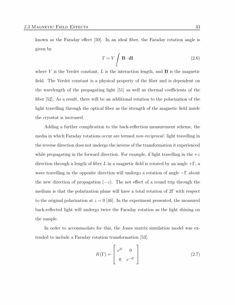
The field gradient curve, shown in Fig. 2–3, was provided by the manufacturer of
the superconducting magnet. It describes the magnetic field strength as a function
of position along the z-axis of the cryostat. The provided curve was derived for
the maximum field strength of the magnet, 9 T, where∫
LB · dl ≈ 1.08 m T was
found by numerical integration of the field gradient. The gradient shows a fairly
sharp cutoff; therefore the integral in Eq. 2.6 can be reasonably approximated by a
uniform magnetic field B over a fixed length l, as shown in Fig. 2–3.
Γ = V
∫
L
B(l) · dl ≈ V Bl (2.10)
To compare the experimental data with the simulations, the initial fitting parameters
φ, ψ, θ were found for the α−β map acquired at B = 0 T. Fixing these parameters,
two other α− β maps were produced at different magnetic field strengths.
2.3 Magnetic Field Effects 35
Figure 2–3: Magnetic field gradient along the z-axis inside the cryostatwhere z = 0 corresponds to the centre of the superconducting magnet. Theshaded region denotes the area of the field where the optical fiber is presentstarting at z = 0.019 m. The box shows the approximation of a uniformmagnetic field B over a length l = 0.12 m. The area enclosed by the rectangleis equal to the area under the curve in the field profile.
Using this approximation, the amount of Faraday rotation per Tesla can be
used as a fitting parameter for the simulation, where Γ/B = V l. A result of this
approximation is that changes in V and l are indistinguishable, so the collective term
V l is used. This makes it possible to match the changes in the polarization maps as
a function of magnetic field, as illustrated in Fig. 2–4.
The experimental data and simulations match up well in both location and shape
at each of the magnetic fields tested for fiber parameters φ, ψ, θ = 0.28π, 0.2π, 1.1π
and V l = 0.06 ± 0.005 radT−1. These values were found by fitting the parameters
by inspection to match up with the corresponding experimental maps. The error in
V l comes from the qualitative analysis where the values within that range produce
reasonable agreement with the experimental data. It should be noted that the exper-
imental data shows a decrease in the peak to peak signal amplitude as the magnetic
2.3 Magnetic Field Effects 36
(a) Experiment
(b) Simulation
Figure 2–4: Contour maps showing the polarization controller output indifferent magnetic fields. (a) Maps of experimental data (T ≈ 270 mK) and(b) the corresponding Jones matrix simulations. As the magnetic field isincreased, the regions of circularly polarized light begin to rotate counter-clockwise and become distorted.
field strength is increased. The origin of this behaviour is not well understood at this
time, however, it is speculated that the efficiency of the controller may be related to
the non-uniformity and non-linearity of the magnetic field along the optical fiber.
A search of the literature was conducted to find comparative results but no re-
sults were found in a similar temperature regime. The work by Williams et al. showed
that the Verdet constant of SiO2 optical fibers has a positive linear relationship with

2.4 Conclusions 37
temperature in the range of 293−423 K, but no work was conducted at lower temper-
atures [52]. There was no indication in the literature that using Becquerel’s formula
to approximate the Verdet constant at the extreme temperatures of the apparatus
is valid. As a result, using the same numerical estimation was unfeasible. Although
a direct comparison of these results are not possible at this time, the value from the
Jones matrix model agrees with the trend that a smaller value of V l will result at
low-temperatures.
2.4 Conclusions
In this chapter the design and operation of our cryogenic polarization controller
for near infrared laser light using a back-reflection measurement technique was de-
scribed. A Jones matrix model was presented to verify the operation of the controller
with and without exposure to a strong magnetic field. When operating in a mag-
netic field, the light travelling through the optical fiber undergoes a Faraday rotation
that produces an offset in the polarization measured with the back-reflected signal
in comparison to the output at the end of the fiber. This understanding will prove
invaluable when using the controller to conduct magneto-optical transport measure-
ments in quantum Hall samples, which will be discussed in Chapter 3.

CHAPTER 3
Magneto-optical Quantum TransportMeasurements
The nuclear spins of GaAs have showed great promise as quantum infor-
mation carriers [4], but the main hindrance to their implementation lies in
the ability to control and retrieve the information from their quantum mechanical
states. In this chapter an investigation will be conducted on the use of the cryo-
genic polarization controller presented in Chapter 2 to manipulate the properties of
a GaAs/AlGaAs quantum well in the first Landau level of the integer quantum Hall
state.
3.1 Experiment
3.1.1 Apparatus
In order to reach the low temperatures required to perform the transport mea-
surements, a commercial 3He refrigerator (Janis HE-3-SSV) was used to work at a
base temperature of T ≈ 270 mK. A copper bar was thermally attached to the 3He
chamber of the fridge and a sample mount was constructed out of G10 to place the
sample in the centre of the magnetic field profile. To thermally link the sample to
38

3.1 Experiment 39
the fridge, it was placed on top of a copper plate that is directly connected to the
copper bar below the 3He pot.
As described in Chapter 2, the light from the polarization controller is directed
into the sample through an optical fiber. The fiber is fed into the cryostat using a
vacuum feedthrough and sealed using epoxy to preserve the integrity of the vacuum
space. The remainder of the fiber was passed down into the chamber of the vacuum
can. In order to accommodate any accidental breakages that may occur at the end
of the fiber, an extra length of approximately 0.5 m was looped and loosely fixed
to the exterior of the charcoal sorb. The loop was maintained with a diameter of
approximately 8 cm to prevent any losses that could occur if the fiber was bent past
its critical angle. The charcoal sorb’s position outside of the magnetic field gradient,
as in Fig. 3–1, makes it ideal for mounting the loop. Since it is outside of the B
field, no Faraday rotation occurs in this portion of the fiber. The balance of the fiber
was then passed through the magnetic shield and held approximately 1 cm above the
sample surface. The light emanating from the end of the fiber is unfocused and, as
a result, this position above the sample provides a beam spot that covers as much of
the surface as possible.
3.1.2 Optics Calibration
In these experiments, the laser used was a 10 mW diode (L808P010) with a
wavelength λ ≈ 800 nm. Barrett showed that this was an ideal wavelength for
dynamically polarizing GaAs nuclei [25]. Prior to cooling, the optical system was
aligned and the output power calibrated to the laser diode driving current. A power
meter (Newport model 815) was placed in front of the fiber’s output. A small guide,
illustrated in Fig. 3–2, was constructed from heavy stock paper and placed over the
sensor to maintain the fiber’s alignment with the detector and to block out a majority

3.1 Experiment 40
Figure 3–1: Illustration of the cryogenic environment in the Janis HE-3-SSV system. The inset on the left demonstrates how the optical fiber(shown in red) is fixed above the sample surface. The vertical magnetic fieldgradient provided by Janis is shown along the length of the cryostat. Thishelps demonstrate that the loop of fiber attached to the charcoal sorb is outof the B field.
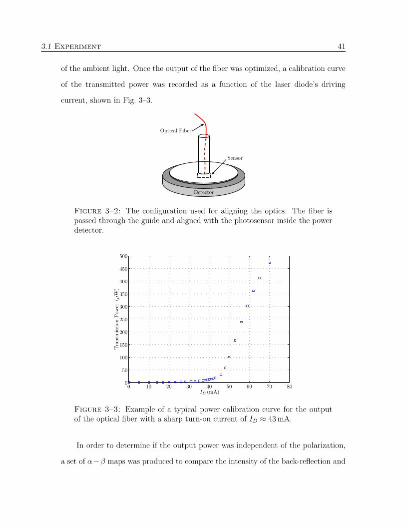
3.1 Experiment 41
of the ambient light. Once the output of the fiber was optimized, a calibration curve
of the transmitted power was recorded as a function of the laser diode’s driving
current, shown in Fig. 3–3.
Figure 3–2: The configuration used for aligning the optics. The fiber ispassed through the guide and aligned with the photosensor inside the powerdetector.
Figure 3–3: Example of a typical power calibration curve for the outputof the optical fiber with a sharp turn-on current of ID ≈ 43 mA.
In order to determine if the output power was independent of the polarization,
a set of α−β maps was produced to compare the intensity of the back-reflection and

3.1 Experiment 42
transmission signals. From the maps in Fig. 3–4, one notes that the power fluctuates
by approximately 8% as the waveplates are rotated. However, there does not appear
to be a direct correlation between power and polarization.1
(a) Back-reflection (b) Transmission
Figure 3–4: Room temperature α− β maps of (a) back-reflection and (b)transmission intensity. In certain map regions, there is a fluctuation in powerof approximately 8%.
3.1.3 GaAs/AlGaAs Quantum Well
For the entirety of the experiments presented, a small sample (approximately
5 mm × 5 mm) cut from a GaAs/AlGaAs wafer prepared by our collaborators was
used.2 The wafer was grown using molecular beam epitaxy to form a 30 nm wide
well according to the procedure outlined in Fig. A–2 in Appendix A. The full band
1 After this work was completed, more recent measurements have demonstratedthat there may in fact be a correlation between polarization and transmission power,although the source of this is unknown at the time of publishing. Further investiga-tion into this relationship is ongoing.
2 J. L. Reno and M. P. Lilly at Sandia National Laboratories, Center for IntegratedNanotechnologies (CINT), in Albuquerque, NM, USA
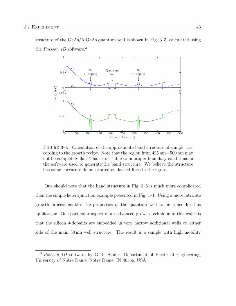
3.1 Experiment 43
structure of the GaAs/AlGaAs quantum well is shown in Fig. 3–5, calculated using
the Poisson 1D software.3
Figure 3–5: Calculation of the approximate band structure of sample ac-cording to the growth recipe. Note that the region from 425 nm−500 nm maynot be completely flat. This error is due to improper boundary conditions inthe software used to generate the band structure. We believe the structurehas some curvature demonstrated as dashed lines in the figure.
One should note that the band structure in Fig. 3–5 is much more complicated
than the simple heterojunction example presented in Fig. 1–1. Using a more intricate
growth process enables the properties of the quantum well to be tuned for this
application. One particular aspect of an advanced growth technique in this wafer is
that the silicon δ-dopants are embedded in very narrow additional wells on either
side of the main 30 nm well structure. The result is a sample with high mobility
3 Poisson 1D software by G. L. Snider, Department of Electrical Engineering,University of Notre Dame, Notre Dame, IN 46556, USA
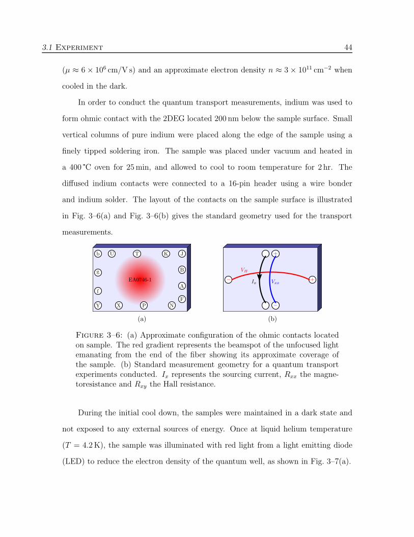
3.1 Experiment 44
(µ ≈ 6 × 106 cm/V s) and an approximate electron density n ≈ 3 × 1011 cm−2 when
cooled in the dark.
In order to conduct the quantum transport measurements, indium was used to
form ohmic contact with the 2DEG located 200 nm below the sample surface. Small
vertical columns of pure indium were placed along the edge of the sample using a
finely tipped soldering iron. The sample was placed under vacuum and heated in
a 400 °C oven for 25 min, and allowed to cool to room temperature for 2 hr. The
diffused indium contacts were connected to a 16-pin header using a wire bonder
and indium solder. The layout of the contacts on the sample surface is illustrated
in Fig. 3–6(a) and Fig. 3–6(b) gives the standard geometry used for the transport
measurements.
(a) (b)
Figure 3–6: (a) Approximate configuration of the ohmic contacts locatedon sample. The red gradient represents the beamspot of the unfocused lightemanating from the end of the fiber showing its approximate coverage ofthe sample. (b) Standard measurement geometry for a quantum transportexperiments conducted. Ix represents the sourcing current, Rxx the magne-toresistance and Rxy the Hall resistance.
During the initial cool down, the samples were maintained in a dark state and
not exposed to any external sources of energy. Once at liquid helium temperature
(T = 4.2 K), the sample was illuminated with red light from a light emitting diode
(LED) to reduce the electron density of the quantum well, as shown in Fig. 3–7(a).

3.1 Experiment 45
Typically, illuminating a 2DEG sample with photons of near bandgap energy
results in an increase in the well’s electron density. This is generally due to the
photoexcitation of the DX centres of the AlxGa1−xAs layer, or through electron-hole
generation in the bulk GaAs with a charge separation at the interface. At liquid
helium temperatures this positive density change is stable and can only be decreased
by significant heating [54]. This is known as Positive Persistent Photoconductivity
(PPPC).
In this sample, a permanent decrease in the quantum well’s electron density
was observed after it has been illuminated with red light from a LED. Negative
Photoconductivity (NPC) has been reported previously but normally the density
was found to increase again after the photoexcitation was removed [54, 55]. Chaves
proposed an explanation for NPC and argues that it originates from the optical
excitation of electron-hole pairs in the large gap layer and their spatial separation due
to the heterojunction’s inherent electric field. For quantum well structures with large
undoped spacer regions (Ls ≥ 40 nm), such as those found in this sample, the negative
photoconductivity can persist for minutes or much longer [56]. This model could
account for the Negative Persistent Photoconductivity (NPPC) that was observed
in our sample.
It was observed that the density shift remains after a cycle in temperature from
T ≈ 0.27 K − 4.2 K but returns to an electron density near that of the dark state
after the sample was allowed to warm to T ≈ 40 K, as shown in Fig. 3–7(b).

3.2 Polarization Dependence Sweeps 46
(a) (b)
Figure 3–7: (a) Trace of the magnetoresistance as a function of magneticfield before and after the sample was illuminated by the LED. Exposing thesample to 225µAs (2×1.5µA for 75 s) was usually enough to bring the ν = 1quantum Hall state within the range of the system’s magnet. (b) Densityreturns to near that of the dark state after the sample is warmed to T ≈ 40 K.Both traces were taken at base temperature T ≈ 270 mK.
3.2 Polarization Dependence Sweeps
Once the sample reached an electron density where the valley of ν = 1 was
located near B ≈ 6.5 T − 7 T, the laser was turned on and the driving current
was slowly increased while the sample was grounded. In order to avoid shocking
the electrons in the 2DEG, the current was slowly increased until reaching ID ≈
42 mA. This produces a transmission power of approximately 30µW according to
the calibration curve for this specific cooldown, shown in Fig. 3–3.
After the sample was cooled to base temperature, the quality of each of the
contacts was determined using the circuit shown in Fig. A–1 of Appendix A. After
determining the quality of the contacts, B field sweeps were performed on numerous
permutations of I+x ,I−x , V +
xx and V −xx to find the configuration that produced the best
measurement of the quantum Hall state. For all experiments, a sourcing current
Ix = 100 nA was used and measurements of Vxx and Vxy were performed by standard

3.2 Polarization Dependence Sweeps 47
lock-in techniques using either a digital (Stanford SRS-830) or an analog (PAR 124)
amplifier.
Once the best contact configuration was ascertained, the magnetic field was
moved to the flank of the ν = 1 quantum Hall state, as shown in Fig. 3–8(a). After
changing the magnetic field, the sample was left to stabilize for 10 − 15 minutes to
accommodate for any temperature fluctuations that may have occurred due to eddy
currents. Normally, a α− β map would be produced after any significant change in
B due to the considerations discussed in Chapter 2, but in this case the experiment
was conducted before the effect of Faraday rotation was completed and therefore
no map at the exact measurement field is available. The map of the back-reflection
signal in Fig. 3–8(b) was produced at B = 5.6 T. It is known from Chapter 2 that
the Faraday rotation due to 1 T will not significantly change the map and this should
be a good representation of the map at B = 6.77 T.
(a) (b)
Figure 3–8: (a) ν = 1 quantum Hall state of the 2DEG. The red circlehighlights the approximate location of the optical transport measurements.(b) A contour map of back-reflection intensity measuring the output polar-ization at B = 5.6 T.
Ideally, a slice along the vertical of the α − β map would be chosen such that
the output would cycle through regions of circular (σ+ and σ−) and linearly (||)
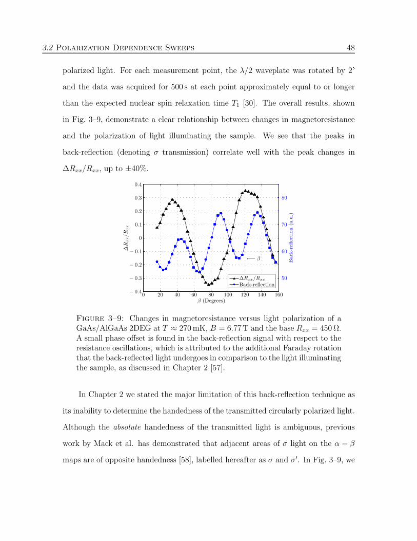
3.2 Polarization Dependence Sweeps 48
polarized light. For each measurement point, the λ/2 waveplate was rotated by 2°and the data was acquired for 500 s at each point approximately equal to or longer
than the expected nuclear spin relaxation time T1 [30]. The overall results, shown
in Fig. 3–9, demonstrate a clear relationship between changes in magnetoresistance
and the polarization of light illuminating the sample. We see that the peaks in
back-reflection (denoting σ transmission) correlate well with the peak changes in
∆Rxx/Rxx, up to ±40%.
Figure 3–9: Changes in magnetoresistance versus light polarization of aGaAs/AlGaAs 2DEG at T ≈ 270 mK, B = 6.77 T and the base Rxx = 450 Ω.A small phase offset is found in the back-reflection signal with respect to theresistance oscillations, which is attributed to the additional Faraday rotationthat the back-reflected light undergoes in comparison to the light illuminatingthe sample, as discussed in Chapter 2 [57].
In Chapter 2 we stated the major limitation of this back-reflection technique as
its inability to determine the handedness of the transmitted circularly polarized light.
Although the absolute handedness of the transmitted light is ambiguous, previous
work by Mack et al. has demonstrated that adjacent areas of σ light on the α − β
maps are of opposite handedness [58], labelled hereafter as σ and σ′. In Fig. 3–9, we

3.3 2D Maps of Resistance and Polarization 49
see that adjacent peaks in back-reflection correspond to changes of Rxx in opposite
directions.
3.3 2D Maps of Resistance and Polarization
The observations presented in the previous section demonstrate that a clear
relationship exists between Rxx and the polarization of the light incident on the
2DEG. In an attempt to make these results more robust, similar experiments were
repeated through a number of slices along the α−β map to produce a two-dimensional
picture of the relationship between resistance and polarization.
For these experiments, the same procedure outlined in Section 3.2 was used.
The B field was set on the right flank of ν = 1 with a base resistance of Rxx ≈ 360 Ω.
For measurements along the vertical cuts of the α−β map, the λ/4 waveplates were
set to a fixed value and the λ/2 waveplate was rotated in 2° steps. The angles of
the λ/4 waveplates were then rotated by 5° and the measurements were repeated
along a new β slice. In Fig. 3–10 we see the results as two dimensional maps of the
back-reflection signal and corresponding changes in magnetoresistance.
The correlation between illuminating the sample with circularly polarization and
changes in Rxx are even more apparent in the 2D maps. The regions of circularly
polarized transmission on the back-reflection map correspond directly with changes
in ∆Rxx/Rxx. The regions labelled σ both have the same handedness and correspond
a positive change in resistance. Conversely, the regions labelled σ′ correspond to a
negative change in resistance.
If one looks closer at the Zeeman energy model given by Eq. 1.13, one can see
that a change in the mean nuclear spin polarization 〈I〉 can be detected using the
magnetoresistance Rxx. If one follows Paget’s result in Eq. 1.42 where 〈I〉 ∝ −P, it

3.4 Dynamics Experiments 50
(a) Back-reflection (b) Magnetoresistance
Figure 3–10: Two α − β maps of (a) back-reflection and (b) ∆Rxx/Rxx.The regions labelled σ and σ′ represent transmission of a different handednessof circularly polarized light. T ≈ 270 mK, B = 6.770 T, P ≈ 72µW poweroutput from the fiber .
can be seen that pumping the sample with σ+ should result in 〈I〉 < 0 and pumping
with σ− should result in 〈I〉 > 0.
Looking closer at the Zeeman energy Ez = g∗µB (B +BN )Sz, where BN =
A 〈Iz〉 /g∗µB, one can see that a change in 〈I〉 will affect the magnitude and sign
of the Overhauser shift BN . If 〈I〉 > 0, the Zeeman energy will decrease because
BN will be in opposition to B. If 〈I〉 < 0, the result is an increase in the Zeeman
energy gap because B and BN are in the same direction. In the thermally activated
region of ν = 1, this change in the Zeeman gap energy ∆ should be detectable as a
change in magnetoresistance where Rxx ∝ e−∆/2kBT (see Eq. 1.14). Therefore, the
changes in Rxx that are seen as a result of different polarizations may be indicative
of polarized nuclei.
3.4 Dynamics Experiments
In the previous two sections, it has been demonstrated that a link exists be-
tween the polarization of light used to illuminate the GaAs/AlGaAs 2DEG and the

3.4 Dynamics Experiments 51
magnetoresistance Rxx of the ν = 1 Landau level of the quantum Hall system. The
following section describes a series of dynamics experiments that were conducted to
probe the origins of this relationship.
To perform these measurements, the system was set up in a similar fashion to
the optical sweeps described previously. A α − β map of the back-reflection signal
was produced after the B field was set on the flank of ν = 1. Using the map in
Fig. 3–11(a) as a guide, a vertical slice of β was found that traverses through regions
of both σ and || output. The waveplates were then set to a σ region and allowed
to stabilize for a minimum of 500 s. While recording the magnetoresistance, the λ/2
waveplate was quickly rotated (< 1 s) using the computer controlled stepper motor
to change the output to a region of linear polarization. In Fig. 3–11(b), the results
of the first such dynamics measurement are seen. The fiber’s output polarization
was changed to a linear state at t = 0 s resulting in a behaviour that clearly follows
an exponential decay, with an overall ∆Rxx ≈ −95 Ω and a decay time constant of
τ1 = 340 ± 10 s.
(a) (b)
Figure 3–11: (a) α − β map of back-reflection at B = 7.1561 T. (b)A measurement of the magnetoresistance decay as the polarization of lightilluminated on the sample was changed from σ to || at t = 0 s.

3.4 Dynamics Experiments 52
In subsequent measurements, the same process was repeated but the polarization
was changed in the opposite direction. In this case, the sample was stabilized under
|| illumination and then the output was quickly changed to σ. Fig. 3–12 depicts
an example result from these experiments. The change in polarization from || → σ
in Fig. 3–12(a) results in a magnetoresistance change of ∆Rxx ≈ +75 Ω and an
exponential behaviour with a time constant of τ ′1 = 360± 20 s. After the sample had
stabilized, the process was reversed and measurements were taken of the transition
from σ → ||, shown in Fig. 3–12(b). Again, one sees an exponential decay with a
time constant of τ1 = 440 ± 20 s and an overall ∆Rxx ≈ −80 Ω. In general, the
process appears to be very reversible and the equilibrium magnetoresistance under
each pumping condition remains the same.
(a) (b)
Figure 3–12: Decay of magnetoresistance near ν = 1 as the polarizationof light shining on the sample is changed at t = 0 s from (a) || → σ and (b)σ → ||.
It should be noted that in the previous experiments, all of the measurements
were performed using σ regions having the same handedness of circularly polarized
light. An additional measurement was taken using a circularly polarized region of
the opposite handedness labelled as σ′ in Fig. 3–11(a). Fig. 3–13 shows the results
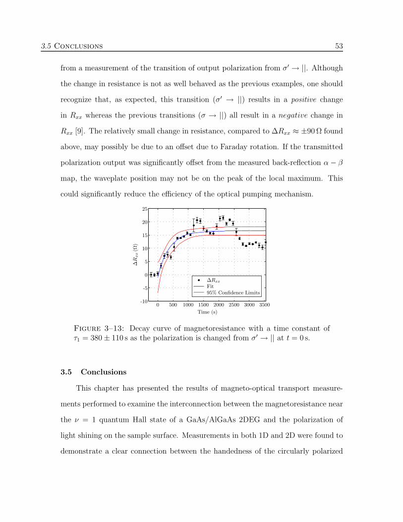
3.5 Conclusions 53
from a measurement of the transition of output polarization from σ′ → ||. Although
the change in resistance is not as well behaved as the previous examples, one should
recognize that, as expected, this transition (σ′ → ||) results in a positive change
in Rxx whereas the previous transitions (σ → ||) all result in a negative change in
Rxx [9]. The relatively small change in resistance, compared to ∆Rxx ≈ ±90 Ω found
above, may possibly be due to an offset due to Faraday rotation. If the transmitted
polarization output was significantly offset from the measured back-reflection α− β
map, the waveplate position may not be on the peak of the local maximum. This
could significantly reduce the efficiency of the optical pumping mechanism.
Figure 3–13: Decay curve of magnetoresistance with a time constant ofτ1 = 380 ± 110 s as the polarization is changed from σ′ → || at t = 0 s.
3.5 Conclusions
This chapter has presented the results of magneto-optical transport measure-
ments performed to examine the interconnection between the magnetoresistance near
the ν = 1 quantum Hall state of a GaAs/AlGaAs 2DEG and the polarization of
light shining on the sample surface. Measurements in both 1D and 2D were found to
demonstrate a clear connection between the handedness of the circularly polarized
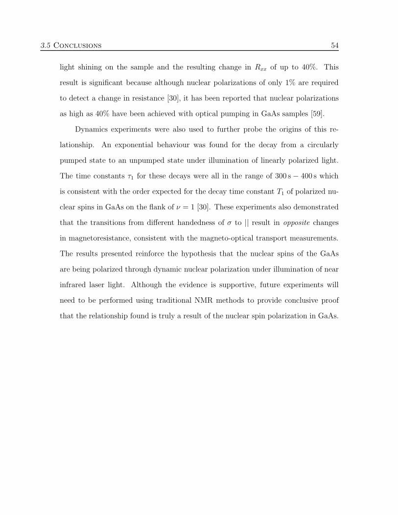
3.5 Conclusions 54
light shining on the sample and the resulting change in Rxx of up to 40%. This
result is significant because although nuclear polarizations of only 1% are required
to detect a change in resistance [30], it has been reported that nuclear polarizations
as high as 40% have been achieved with optical pumping in GaAs samples [59].
Dynamics experiments were also used to further probe the origins of this re-
lationship. An exponential behaviour was found for the decay from a circularly
pumped state to an unpumped state under illumination of linearly polarized light.
The time constants τ1 for these decays were all in the range of 300 s − 400 s which
is consistent with the order expected for the decay time constant T1 of polarized nu-
clear spins in GaAs on the flank of ν = 1 [30]. These experiments also demonstrated
that the transitions from different handedness of σ to || result in opposite changes
in magnetoresistance, consistent with the magneto-optical transport measurements.
The results presented reinforce the hypothesis that the nuclear spins of the GaAs
are being polarized through dynamic nuclear polarization under illumination of near
infrared laser light. Although the evidence is supportive, future experiments will
need to be performed using traditional NMR methods to provide conclusive proof
that the relationship found is truly a result of the nuclear spin polarization in GaAs.

CHAPTER 4
Laser Induced Phenomena inGaAs/AlGaAs Quatum Wells
During the course of the investigations presented in this thesis, an inter-
esting behaviour was observed in the quantum Hall traces of GaAs/AlGaAs
quantum wells exposed to low power near infrared laser light (λ ≈ 800 nm). Under
illumination, a series of unexplained features were found in the Rxx valleys, includ-
ing but not limited to, ν = 1. This chapter presents the preliminary results of an
investigation to uncover the origin of these phenomena.
4.1 Zero Resistance States Under Laser Illumination
While conducting a series of transport measurements to determine the best
set of contacts for a quantum Hall trace, an unexplained series of zero resistance
states was discovered in a magnetic field trace of Rxx. This startling observation
is an immediate reminder of the microwave induced zero resistance states found
in GaAs/AlGaAs 2DEGs by Mani et al. [60]. Although similar in nature, these
experiments were performed in a much different energy regime that in the system
presented here.
55
4.2 Contact Dependence 56
The measurements were repeated recording both Rxx and Rxy to determine the
Landau level filling factor ν of all the zero resistance states in the trace, shown
in Fig. 4–1. It is noted that the features present in Rxx show a strong hysteretic
behaviour with the B field sweep direction. Upon close inspection, it is noted that the
slope of the Hall resistance is not uniform and actually increases at higher magnetic
fields (B > 4 T). Perhaps the most startling result of Fig. 4–1 is that a number of
these zero resistance states do not coincide with plateaus in Rxy as one would expect
in a quantum Hall system (integer or fractional). The Rxy plateaus that do coincide
with a zero resistance state are offset from the centre of the valley. These observations
may suggest an inhomogeneity in the quantum well and that the geometry of the
sample contacts may play an important role in the understanding of these features.
(a) (b)
Figure 4–1: Transport sweeps of Rxx and Rxy with B (a) increasing and(b) decreasing. The dashed red line is a linear fit to the Hall resistance forB < 2 T and extrapolated to show the change in curvature of Rxy at highermagnetic fields.
4.2 Contact Dependence
In order to examine the effects of geometry, the same transport measurements
were repeated using different contact configurations, as shown in Fig. 4–2. The con-
tact maps in the inset of each figure show that each configuration probes a different

4.2 Contact Dependence 57
region of the electron gas. In Fig. 4–2(a) and Fig. 4–2(b), the contacts used for the
source current were switched from the centre of the sample to the left edge, resulting
in a significant difference in slope of the Hall resistance between the two configu-
rations. Overall, this would suggest that the electron density in the centre of the
2DEG is much lower than the density of the left side.
Some of these results are similar to those found by Shields who studied below
bandgap laser excitation in a GaAs/AlGaAs quantum well [61]. While illuminating
different regions of the sample, the Hall resistance was measured to determine the
electron density of the 2DEG and it was found that the local electron density was
reduced in the locality of the laser spot. A significant change in density was observed
with both focused and unfocused light. Although the same curvature in Rxy that
was found in Fig. 4–2 was not seen, only data in the range B = 0 T−4 T is available.
This however is still in the linear range of the data in this experiment.
Shields proposed that for excitation light with energy below the bandgap, the
reduction of the quantum well’s electron density was due to photoexcitation of the
thick GaAs buffer layer. Under illumination, the photoexcited electrons in the buffer
would be swept to the front of the sample and collect at the GaAs/AlGaAs interface
at the top of the buffer layer, whereas the holes would be swept towards the growth
initiation surface.
This process continues until a sufficient amount of charge builds up at the op-
posite ends of the buffer layer to reduce the electric field across the buffer layer,
thereby creating an equilibrium that is dependent on the intensity of illumination.
The resulting photovoltage will act like a depleting back gate bias on the quantum
well by raising the potential of the GaAs/AlxGa1−xAs interface at the top of the

4.2 Contact Dependence 58
(a) (b)
(c)
Figure 4–2: Comparison of transport measurements taken using differentcontact configurations on the GaAs/AlGaAs sample. The only differencebetween (a) and (b) is that the source current is moved from the centre ofthe sample to the left side. In (c) the left side of the sample is probed showingonly a single density.

4.3 Temperature Dependence 59
Figure 4–3: Illustration of the band structure modifications that resultfrom photoexcitation with energy below that of the bandgap. In the illumi-nated region, the build up of charge raises the potential at the GaAs/AlGaAsinterface which acts like a depleting back gate bias and reduces the local elec-tron density in the 2DEG [61].
buffer layer. The electrons will flow away from illuminated regions within the plane
of quantum well, reducing the local density [61].
In terms of magnetoresistance, the critical factor appears to be the geometry
of the four terminal measurement. In Fig. 4–2(a) and Fig. 4–2(b), the contacts for
Ix and Vxx are not physically close to each other and the additional zero resistance
minimas are observed. In Fig. 4–2(c), where the contacts are located closer together,
there appears to be only one clear density present and the trace is more representative
of a traditional quantum Hall sample. These observations appear to point to an
inhomogeneity in the quantum well as a result of laser illumination.
4.3 Temperature Dependence
In order to further understand the origins of these zero resistance states, it is
important to understand the energy scales in which they occur. To accomplish this, a
full series of temperature dependence measurements of the quantum Hall states were

4.3 Temperature Dependence 60
performed up to T ≈ 2.3 K. For each data set, the sample temperature was fixed us-
ing a Lakeshore 340 temperature controller and allowed to reach equilibrium and sta-
bilize for 30 min before sweeping the magnetic field. In each case, the magnetic field
was swept up and down from B = 0 T− 8.5 T at a rate of dB/dt = 0.09376 T min−1.
The sample was allowed to restabilize before sweeping in the opposite direction to re-
duce any heating effects from eddy currents. All measurements were were conducted
at a constant laser driving current ID = 40.05 mA which corresponds to an power
of P ≈ 12µW illuminating the sample. For the remainder of the experiments, the
contact configuration shown in Fig. 4–2(a) was used. The results of the temperature
dependence are shown in Fig. 4–4.
The most apparent feature in Fig. 4–4(a) and Fig. 4–4(b) is that the electron
density of the 2DEG has a very strong dependence on temperature. This is demon-
strated by the gradual shift right of the Rxx valleys as the temperature is increased.
In order to further demonstrate the temperature dependence of the electron density,
the mean density of each sweep was calculated using the location of each Hall plateau
centres even though the slope of Rxy changes with B. The temperature dependence
in Fig. 4–5 indicates that there is a saturation of the electron density in the low and
high temperature ranges.
A simple Boltzmann model can be used extract an energy scale from this tem-
perature dependence data. The optical excitation of the laser will create a steady
state density of holes in the valence band and electrons in the conduction band (exci-
tons) which are in addition to the electrons present in the well prior to illumination.
Assuming that the system is near thermal equilibrium, it is expected that the ratio
of free electrons to excitons will be that of a Boltzmann factor. Using this model, a
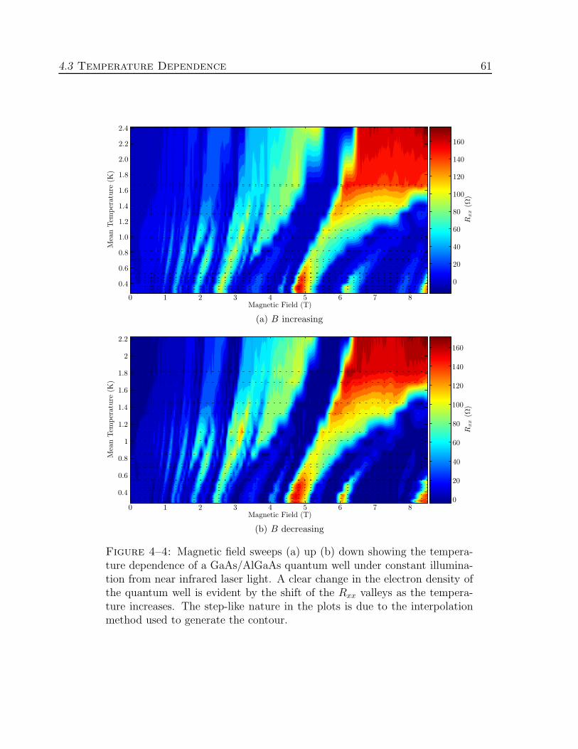
4.3 Temperature Dependence 61
(a) B increasing
(b) B decreasing
Figure 4–4: Magnetic field sweeps (a) up (b) down showing the tempera-ture dependence of a GaAs/AlGaAs quantum well under constant illumina-tion from near infrared laser light. A clear change in the electron density ofthe quantum well is evident by the shift of the Rxx valleys as the tempera-ture increases. The step-like nature in the plots is due to the interpolationmethod used to generate the contour.

4.3 Temperature Dependence 62
crude prediction for the expected density is of the form
n = n0 + nL
e−EbkBT
1 + e−EbkBT
, (4.1)
where n0 is the electron density prior to illumination, nL is the optically generated
total electron density (free electrons and electrons bound to excitons) and Eb is
the binding energy of an exciton. The model in Eq. 4.1 has been applied to the
data in Fig. 4–5 and demonstrates good qualitative agreement to the behaviour of
the electron density over this range of temperatures. Using nL and Eb as fitting
parameters, we can see find a binding energy of Eb ≈ 1.6 K, corresponding to an
energy scale of Eb ≈ 0.34 meV.
The energy scale found as a result of fitting this data to the model in Eq. 4.1 is
not realistic for the exciton binding energy, as it is well below the 5 meV − 20 meV
range expected for excitons in GaAs [62]. In addition to the binding energy, the fit
value for nL is much larger than expected for such a low power laser. It is unlikely
that such a large number of electron hole pairs could be generated by such low power
excitation, due to the short recombination time for excitons.
In Fig. 4–6, it is noted that at high temperatures (T ≈ 2 K) an almost “normal”
quantum Hall trace returns. The Hall resistance once again has a linear slope in Rxy,
without any curvature at high magnetic fields. Although the Landau level valleys
are well defined, the Hall plateaus are still offset from their centre.
The transport measurements in Fig. 4–4 can be adjusted to remove the effect
of the electron density’s temperature dependence. Using the data in Fig. 4–5, the
magnetic field is rescaled by
B′ =n0
n (T )× B (4.2)

4.3 Temperature Dependence 63
Figure 4–5: Demonstration of the temperature dependence of the quantumwell’s electron density. The solid lines are fits to the Boltzmann approxima-tion in Eq. 4.1 with the given fitting parameters.
where n0 is the electron density at the lowest temperature and n (T ) is the mean
density for each sweep. In Fig. 4–7 one sees a much clearer picture of the temperature
dependence of the additional for zero resistance states. This correction brings forth
some subtle features present in the temperature dependence data.
Upon closer inspection of Fig. 4–7, one sees a very complex crossing behaviour
of these additional zero resistance states in the temperature range from T = 0.6 K−
1.4 K. This behaviour appears to be present in the additional zero resistance states
located near the Landau levels with odd filling factors. At high temperatures it is
observed that, as expected, the odd filling factor Landau levels will close due to the
loss of spin splitting. The interesting behaviour is that the additional states shift as
the temperature evolution progresses which is not a result of the main density shift.
The arrow labelled (1) follows the path of a zero resistance state that begins
near ν = 3 and shows that as the temperature increases, the zero resistance gap
crosses over into the ν = 2 valley. A similar behaviour is found along the path of
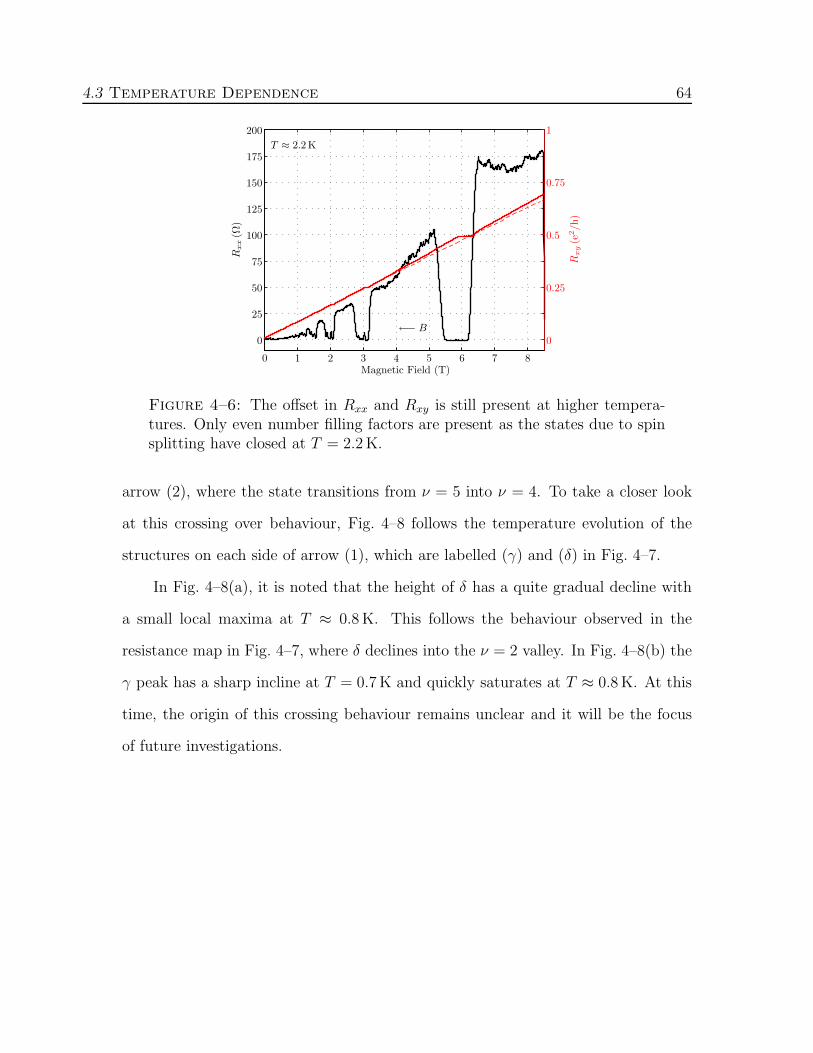
4.3 Temperature Dependence 64
Figure 4–6: The offset in Rxx and Rxy is still present at higher tempera-tures. Only even number filling factors are present as the states due to spinsplitting have closed at T = 2.2 K.
arrow (2), where the state transitions from ν = 5 into ν = 4. To take a closer look
at this crossing over behaviour, Fig. 4–8 follows the temperature evolution of the
structures on each side of arrow (1), which are labelled (γ) and (δ) in Fig. 4–7.
In Fig. 4–8(a), it is noted that the height of δ has a quite gradual decline with
a small local maxima at T ≈ 0.8 K. This follows the behaviour observed in the
resistance map in Fig. 4–7, where δ declines into the ν = 2 valley. In Fig. 4–8(b) the
γ peak has a sharp incline at T = 0.7 K and quickly saturates at T ≈ 0.8 K. At this
time, the origin of this crossing behaviour remains unclear and it will be the focus
of future investigations.

4.3 Temperature Dependence 65
(a) B increasing
(b) B decreasing
Figure 4–7: B field sweeps (a) up and (b) down of the magnetoresistance’stemperature dependence. The data in has been adjusted to compensate forchanges in the well’s electron density.

4.4 Laser Power Dependence 66
(a) Structure δ (b) Structure γ
Figure 4–8: Temperature dependence of the peak height of the structures(γ and δ) on either side of the crossing over gap. In (a) δ shows a slow declinewith temperature, whereas in (b) γ demonstrates a sharp turn behaviour atT = 0.7 K.
4.4 Laser Power Dependence
In the previous section it was found that the behaviour of the GaAs/AlGaAs
quantum well was heavily dependent on the temperature of the sample. One of
the more complicated aspects of these experiments is that the light illuminating the
sample, although very low power, is also heating the electrons in the 2DEG. In this
section, an investigation will be conducted into the effect of changing the output
power of the laser illuminating the sample while maintaining the sample as close to
base temperature as possible. Although the temperature of the bulk sample will be
near that of the base, the electrons in the quantum well are expected to undergo
heating due to photoexcitation.
4.4.1 Reduced Laser Power
In the first part of this experiment, transport measurements were recorded for
each step as the the laser driving current ID was reduced from 40.05 mA to 20 mA.
The procedure for acquiring these measurements was the same as for the temperature
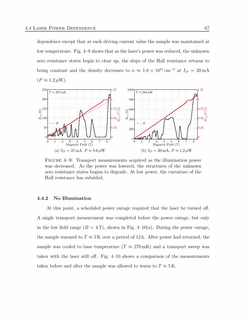
4.4 Laser Power Dependence 67
dependence except that at each driving current value the sample was maintained at
low temperature. Fig. 4–9 shows that as the laser’s power was reduced, the unknown
zero resistance states begin to clear up, the slope of the Hall resistance returns to
being constant and the density decreases to n ≈ 1.8 × 1011 cm−2 at ID = 20 mA
(P ≈ 1.2µW).
(a) ID = 37 mA, P ≈ 8.6 µW (b) ID = 20 mA, P ≈ 1.2 µW
Figure 4–9: Transport measurements acquired as the illumination powerwas decreased. As the power was lowered, the structures of the unknownzero resistance states begins to degrade. At low power, the curvature of theHall resistance has subsided.
4.4.2 No Illumination
At this point, a scheduled power outage required that the laser be turned off.
A single transport measurement was completed before the power outage, but only
in the low field range (B < 4 T), shown in Fig. 4–10(a). During the power outage,
the sample warmed to T ≈ 5 K over a period of 12 h. After power had returned, the
sample was cooled to base temperature (T ≈ 270 mK) and a transport sweep was
taken with the laser still off. Fig. 4–10 shows a comparison of the measurements
taken before and after the sample was allowed to warm to T ≈ 5 K.
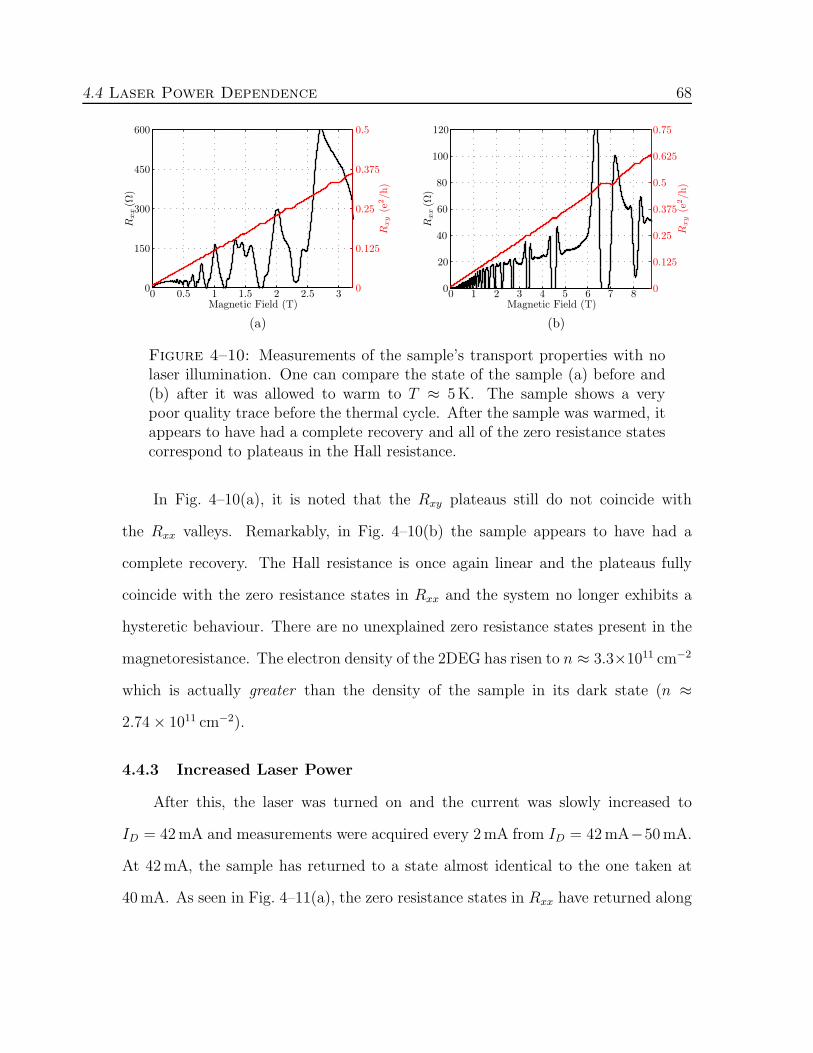
4.4 Laser Power Dependence 68
(a) (b)
Figure 4–10: Measurements of the sample’s transport properties with nolaser illumination. One can compare the state of the sample (a) before and(b) after it was allowed to warm to T ≈ 5 K. The sample shows a verypoor quality trace before the thermal cycle. After the sample was warmed, itappears to have had a complete recovery and all of the zero resistance statescorrespond to plateaus in the Hall resistance.
In Fig. 4–10(a), it is noted that the Rxy plateaus still do not coincide with
the Rxx valleys. Remarkably, in Fig. 4–10(b) the sample appears to have had a
complete recovery. The Hall resistance is once again linear and the plateaus fully
coincide with the zero resistance states in Rxx and the system no longer exhibits a
hysteretic behaviour. There are no unexplained zero resistance states present in the
magnetoresistance. The electron density of the 2DEG has risen to n ≈ 3.3×1011 cm−2
which is actually greater than the density of the sample in its dark state (n ≈
2.74 × 1011 cm−2).
4.4.3 Increased Laser Power
After this, the laser was turned on and the current was slowly increased to
ID = 42 mA and measurements were acquired every 2 mA from ID = 42 mA−50 mA.
At 42 mA, the sample has returned to a state almost identical to the one taken at
40 mA. As seen in Fig. 4–11(a), the zero resistance states in Rxx have returned along
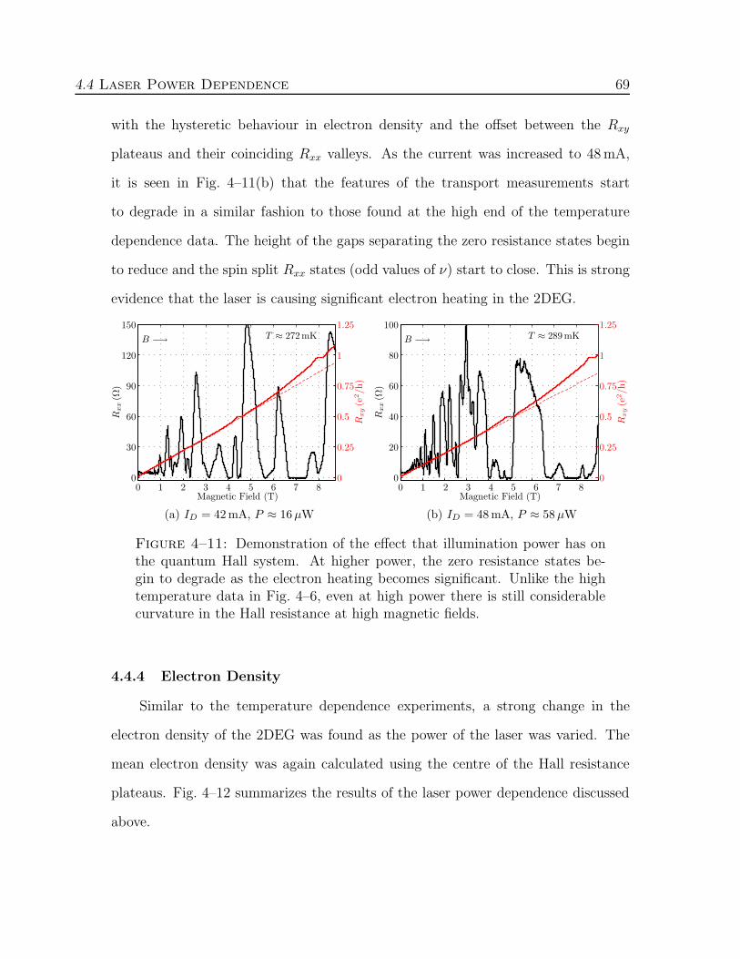
4.4 Laser Power Dependence 69
with the hysteretic behaviour in electron density and the offset between the Rxy
plateaus and their coinciding Rxx valleys. As the current was increased to 48 mA,
it is seen in Fig. 4–11(b) that the features of the transport measurements start
to degrade in a similar fashion to those found at the high end of the temperature
dependence data. The height of the gaps separating the zero resistance states begin
to reduce and the spin split Rxx states (odd values of ν) start to close. This is strong
evidence that the laser is causing significant electron heating in the 2DEG.
(a) ID = 42 mA, P ≈ 16 µW (b) ID = 48 mA, P ≈ 58 µW
Figure 4–11: Demonstration of the effect that illumination power has onthe quantum Hall system. At higher power, the zero resistance states be-gin to degrade as the electron heating becomes significant. Unlike the hightemperature data in Fig. 4–6, even at high power there is still considerablecurvature in the Hall resistance at high magnetic fields.
4.4.4 Electron Density
Similar to the temperature dependence experiments, a strong change in the
electron density of the 2DEG was found as the power of the laser was varied. The
mean electron density was again calculated using the centre of the Hall resistance
plateaus. Fig. 4–12 summarizes the results of the laser power dependence discussed
above.
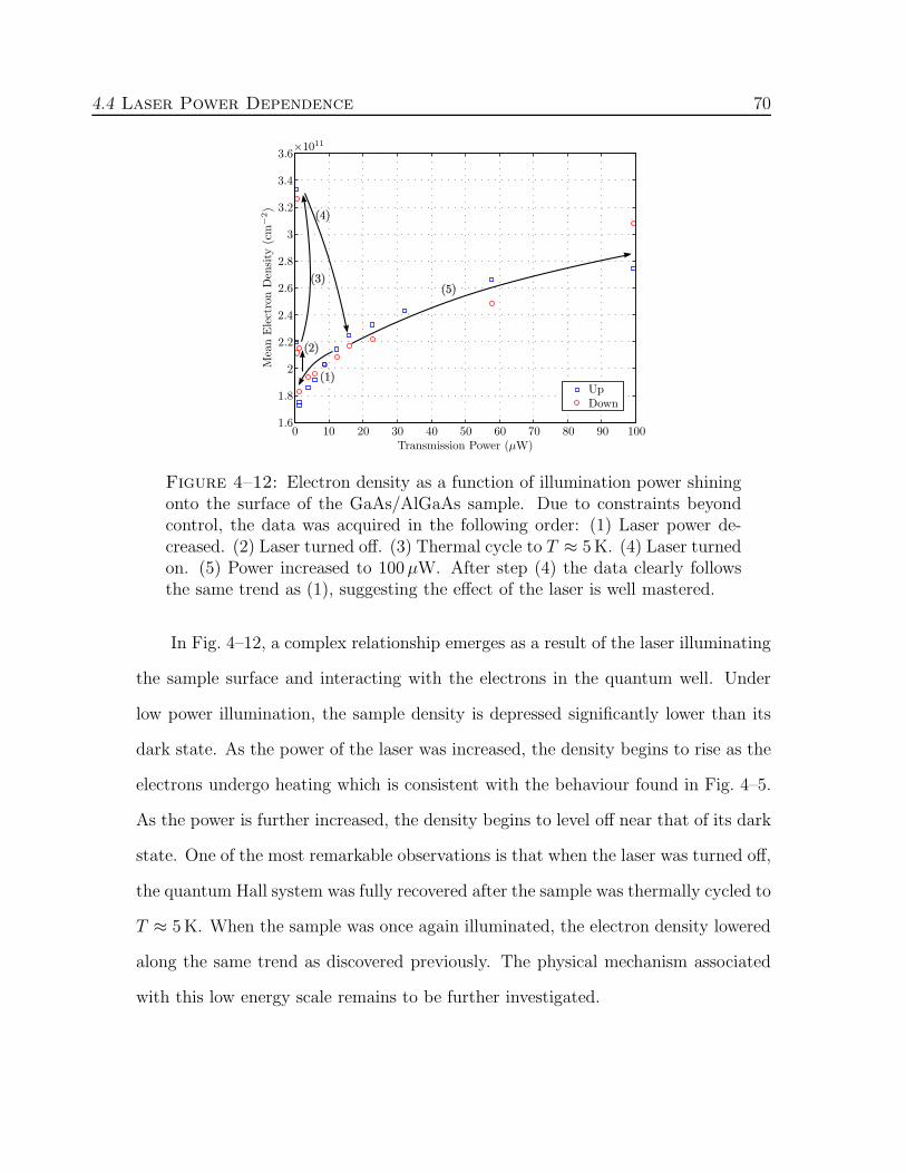
4.4 Laser Power Dependence 70
Figure 4–12: Electron density as a function of illumination power shiningonto the surface of the GaAs/AlGaAs sample. Due to constraints beyondcontrol, the data was acquired in the following order: (1) Laser power de-creased. (2) Laser turned off. (3) Thermal cycle to T ≈ 5 K. (4) Laser turnedon. (5) Power increased to 100µW. After step (4) the data clearly followsthe same trend as (1), suggesting the effect of the laser is well mastered.
In Fig. 4–12, a complex relationship emerges as a result of the laser illuminating
the sample surface and interacting with the electrons in the quantum well. Under
low power illumination, the sample density is depressed significantly lower than its
dark state. As the power of the laser was increased, the density begins to rise as the
electrons undergo heating which is consistent with the behaviour found in Fig. 4–5.
As the power is further increased, the density begins to level off near that of its dark
state. One of the most remarkable observations is that when the laser was turned off,
the quantum Hall system was fully recovered after the sample was thermally cycled to
T ≈ 5 K. When the sample was once again illuminated, the electron density lowered
along the same trend as discovered previously. The physical mechanism associated
with this low energy scale remains to be further investigated.
4.5 Conclusions 71
4.5 Conclusions
This chapter presents the preliminary results of an investigation into the zero
resistance state phenomena in the quantum Hall structure of a GaAs/AlGaAs quan-
tum well under laser illumination. Under photoexcitation, it was observed that these
states appear to be dependent on contact geometry used for conducting the mea-
surements as the laser appears to locally modify the electron density of the quantum
well [61]. A temperature dependence of the transport properties revealed that under
constant illumination, the electron density of the 2DEG increases as a function of
temperature following the behaviour of a Boltzmann two level system with energy
gap Eb ≈ 1.6 K. Normalizing the magnetoresistance curves to account for the den-
sity change reveals that some of the additional zero resistance states demonstrate a
crossing over behaviour as the system’s temperature was increased.
A complex behaviour in the sample’s electron density also developed when the
power of the light shining on the sample was varied. Under low power illumination,
the density of 2DEG was significantly depressed in comparison to its dark state. As
the power was increased, the electron density began to accrue, tending towards a
saturation point near that of the dark state. The modifications caused by the laser
to the quantum Hall state were found to be almost completely reversible under the
thermal cycle conditions of T ≈ 5 K.

CHAPTER 5
Conclusions
5.1 Summary
Tthe potential of using the nuclear spins of GaAs as quantum infor-
mation carriers was introduced in Chapter 1 and a number of topics related
to their implementation were reviewed: GaAs/AlGaAs quantum well structures,
the classical and integer quantum Hall effects, resistively detected nuclear magnetic
resonance and dynamic nuclear polarization through optical pumping methods. In
Chapter 2 the design and implementation of a cryogenic polarization controller that
can output different polarization of light at the end of a standard single mode op-
tical fiber was demonstrated. A model was devised to describe its operation with
and without the presence of a magnetic field. In Chapter 3 the results of magneto-
optical transport measurements show evidence of a direct relationship that exists
between the polarization of the light illuminating the sample and the magnetoresis-
tance of the ν = 1 flank in a GaAs/AlGaAs quantum Hall system were reported.
Dynamics experiments to determine the decay rates of the pumped states were also
performed demonstrating evidence that this behaviour may be due to the dynamic
72
5.2 Future Research 73
polarization of the GaAs nuclear spins as a result of the circularly polarized photoex-
citation. Chapter 4 reports on the observation of a complex series of zero resistance
states in the quantum Hall structure under low power laser illumination. A thor-
ough investigation into the sample’s dependence on contact geometry, temperature
and illumination power was presented and possible explanations were discussed.
5.2 Future Research
Although many of the results presented here show great progress towards the
realization of GaAs as a quantum information carrier, further work is required to
verify (i) that the power of the light exiting the fiber remains constant under all
polarization conditions at low temperatures; (ii) that the nuclear spins are, in fact,
being influenced by polarized photoexcitation; and (iii) the reproducibility of the
laser induced zero resistance states. The following sections briefly explore each of
these future research directions.
5.2.1 Nuclear Magnetic Resonance
In Chapter 3, a strong correlation was found between the ∆Rxx and the light’s
polarization [57]. In addition, the dynamics experiments found that the decay rates
of these pumped states were in good agreement with those expected for the nuclear
spin-lattice relaxation time of GaAs at T ≈ 270 mK. To fully verify that these
observations are a result of nuclear spin polarization, a coil must be installed around
the sample to perform traditional resistively detected NMR experiments. While
maintaining the sample in a circularly pumped state, the frequency of the radio-
frequency oscillations applied to the NMR coil should be swept through the Larmor
frequencies of the isotopes present in GaAs. If the nuclei are in fact polarized,
sweeping through the Larmor resonance frequencies will destroy the induced nuclear
5.2 Future Research 74
polarization, resulting in a measurable change in Rxx. This would provide irrefutable
proof that the system presented is dynamically polarizing the nuclear spins of the
GaAs quantum well.
5.2.2 Polarization Controller
In order to validate the correlation between ∆Rxx and polarization, the effect of
thermal changes on the system must be further investigated. A thorough character-
ization of the polarization controller’s output at low temperatures will be required
to ensure that the power of the light shining on to the sample is independent of po-
larization. The sensitivity of the quantum Hall state to small changes in the output
power should also be investigated to determine the extent that could influence the
system.
One of the key limitations to the current polarization controller design is its
inability to measure the output power of the light shining on the sample. Although
the intensity of the back-reflected light is directly proportional to the intensity of the
fiber’s output, it cannot provide an absolute measure of the output power because it
is dependent on a number of other variables. One proposed solution is to install near
the sample surface a bolometer that is exposed to some of the light originating from
the fiber. A bolometer is typically a temperature sensitive resistor that is heated
by incoming radiation and cooled by the thermal conduction of its electrical wires
[63–68]. Once calibrated, a bolometer mounted near the sample would provide an in
situ method of measuring the absolute output power of the light exiting the fiber.
Additionally, this could act as a means of correcting small misalignment of the optical
system without requiring the system to be warmed to room temperature.

5.2 Future Research 75
5.2.3 Laser Induced Phenomena
Although the investigation presented in Chapter 4 has resulted in a number of
interesting and astonishing observations, the true origin of these laser induced zero
resistance states presently remains unclear. Future experiments are planned using a
small Hall bar sample made from the same wafer as that used in these experiments,
as shown in Fig. 5–1.
Figure 5–1: Illustration of a Hall bar sample with a width of 100µm. Thecontact arms, shown in blue, are patterned using standard photolithographytechniques.
Using the Hall bar should help to eliminate some of the uncertainty related to
the size of the quantum well sample. The smaller area Hall bar may help reduce,
to some extent, the inhomogeneity of the quantum well’s electron density while
under illumination. Similar measurements to those presented here will be conducted
to determine the reproducibility of the behaviour demonstrated by additional zero
resistance states as a function temperature and of illumination power. It is hoped
that these future endeavours will help unravel the origins of these laser induced zero
resistance phenomena.

APPENDIX A
Further Details
A.1 Contact Quality Circuit
The circuit shown in Fig. A–1 was used to verify the quality of each contact
on the sample once it was cooled to liquid Helium temperatures (T = 4.2 K). Each
contact was connected as shown and the differential voltage was measured across the
10 kΩ resistor to determine the current flowing through the contact on the sample.
A “good” contact will have current flow of I ≈ 60 nA − 70 nA.
Figure A–1: Diagram of the circuit used to test the quality of the samplecontacts.
76
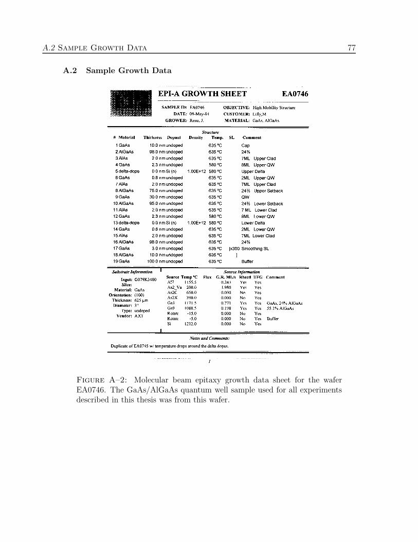
A.2 Sample Growth Data 77
A.2 Sample Growth Data
Figure A–2: Molecular beam epitaxy growth data sheet for the waferEA0746. The GaAs/AlGaAs quantum well sample used for all experimentsdescribed in this thesis was from this wafer.

APPENDIX B
Software Source Code
B.1 Experimental Analysis of α− β MapsAlphaBetaImport.m
1 % This program takes the output f i l e s from BackMotorOptics . v i v2 .0 and parse s
% them for the necessary informat ion to generat e a contour p l o t . I t r e l i e s3 % on a s tandard i zed naming scheme f o r the f i l e s t ha t the so f tware uses .
% Format : (QWP1) (QWP2) . lvm5 % Example : 50 142 . lvm
% Also requ i red i s a constant QWP change d i f f e r e n c e between each of the7 % f i l e s l i c e s ( ’ degree ’ v a r i a b l e ) . The d e f au l t i s 5 degrees .
9 % Simply wr i t e in the d i r e c t o r y conta in ing the data f i l e s , change the date% and f i e l d values , and s e t the QWP l im i t s / increment va lue .
11 clc ;clear ;
13
%%%%%%%%%%%%%% START OF CONFIGURATION %%%%%%%%%%%%%%15 Directory = ’ /Data/2007−03−07/ ba ck r e f l e c t i o n / ’ ; % Data f i l e s .
Date = ’March 7 , 2007 ’ ; % Date o f sweep , f o r p l o t t i t l e .17 f i e l d = 0 ; % B f i e l d , f o r p l o t t i t l e .
f o n t s i z e = 12 ; % Fonts i ze f o r the p l o t axes19 s a v e f i l e s = 1 ; % Save the p l o t s and analyzed data ? (YES=1, NO=0)
QWP1 = [ 70 1 2 5 ] ; % Range of the f i r s t QWP. (Format : [ s t a r t end ] )21 %%%%%%%%%%%%%%% END OF CONFIGURATION %%%%%%%%%%%%%%%
23 degree = 5 ; %Number o f degrees between each data s e t .
25 QWP2 = QWP1+92;numf i l e = (QWP1(2) − QWP1(1) ) / degree ; %Number o f f i l e s to import
27
for j = 1 : numf i l e+129 f i l ename = f u l l f i l e ( Directory , s t r c a t (num2str(QWP1(1)+(j −1)* degree ) , ’ ’ ,ց
→num2str(QWP2(1)+(j −1)* degree ) , ’ . lvm ’ ) ) ;f i d = fopen ( f i l ename ) ;
31 Data ( : , : , j ) = texts can ( f i d , ’%f %f %f ’ , ’ h eade r l i n e s ’ , 21) ;fc lose ( f i d ) ;
33 Z ( : , j ) = ce l l 2mat (Data ( : , 2 , j ) ) ;end
35 % Extrac t the axes l a b e l sY = ce l l 2mat (Data ( : , 1 , 2 ) ) /64 ;
78

B.2 Simulation of α− β Maps and Faraday Rotation 79
37 X= QWP1(1) : degree :QWP1(2) ;
39 f igure (1)contour f (X,Y, Z , 20 , ’ L ineSty l e ’ , ’ none ’ )
41 xlabel ( ’ \ alpha ( Degrees ) ’ , ’ FontSize ’ , f o n t s i z e )ylabel ( ’ \beta ( Degrees ) ’ , ’ FontSize ’ , f o n t s i z e )
43 t i t l e ( [ ’ Back r e f l e c t i on \ alpha − \beta Map, ’ , Date , ’ , F i e ld = ’ , num2str(ց→ f i e l d ) , ’ T ’ ] , ’ FontSize ’ , f o n t s i z e )colorbar
45 grid on
47 % Force proper t i c k l o c a t i on s on the p l o t s .set (gca , ’ XTick ’ ,QWP1(1) : 1 0 :QWP1(2) , ’ XTickLabel ’ ,QWP1(1) : 1 0 :QWP1(2) )
49 set (gca , ’ YTick ’ , 0 : 20 : 180 , ’ YTickLabel ’ , 0 : 20 : 180 )
51 % Format the data in to a s i n g l e matrix which can be e a s i l y imported in to% Orig in i f you pr e f e r to use or i g i n to p l o t t he contour .
53 % Simply uncomment the f o l l ow i n g and run :i f s a v e f i l e s == 1
55 OriginOut ( 2 : length (Y) +1 ,1) = Y;OriginOut ( 1 , 2 : numf i l e+2) = X;
57 OriginOut ( 2 : length (Y) +1 ,2: numf i l e +2) = Z ;csvwrite ( s t r c a t ( Directory , ’AlphaBetaMap− ’ , Date , ’ . csv ’ ) , OriginOut )
59
% Generate and save images in 3 convenient formats .61 [ f i l e p a t h , f i l ename , ext , versn ] = f i l e p a r t s ( D i r ectory ) ;
saveas ( gcf , f u l l f i l e ( f i l e p a t h , s t r c a t ( f i l ename , ’AB Map . pdf ’ ) ) ) ;63 saveas ( gcf , f u l l f i l e ( f i l e p a t h , s t r c a t ( f i l ename , ’AB Map . f i g ’ ) ) ) ;
saveas ( gcf , f u l l f i l e ( f i l e p a t h , s t r c a t ( f i l ename , ’AB Map . png ’ ) ) ) ;65 end
B.2 Simulation of α− β Maps and Faraday Rotation
simulate.m
1 % This func t ion i s used to generat e s the s imula t ion of the po l a r i z a t i on% con t ro l l e r ’ s back−r e f l e c t i o n i n t e n s i t y .
3 %% Syntax : s imu la t e ( p la t e , faraday , f i b e r , b f i e l d )
5 %% where b f i e l d = magnetic f i e l d s t r eng t h
7 % p l a t e = s t r u c t ( ’HWPmin’ ,HWPmin, ’HWPmax’ ,HWPmax, ’QWPmin’ ,QWPmin, ’ց→QWPmax’ ,QWPmax) ;% faraday = s t r u c t ( ’ lambda0 ’ , lambda0 ’ , ’ l eng th ’ , Blength ) ;
9 % f i b e r = s t r u c t ( ’ t he t ’ , t he t , ’ phi ’ , phi , ’ t h i ’ , t h i ) ;%
11 % Last modi f ied : October 2007% Copyright 2007 Jonathan M. Buset
13 function SimOut=s imulate ( plate , faraday , f i b e r , b f i e l d )% Loop over the HWP ( be ta )
15 for e = p l a t e .HWPmin: 5 : p l a t e .HWPmax% Loop over the f i r s t QWP ( alpha )
17 for f = p l a t e .QWPmin : 5 : p l a t e .QWPmaxa=1* f *pi /180;
19 b=−1*(e ) *pi /180;c=1*( f +180)*pi /180;
21
% Generate p o l a r i z a t i on23 amplitude = jones (a , b , c , p late , faraday , f i b e r , b f i e l d ) ;
% Calcu la t e the i n t e n s i t y25 Output ( ( e /5)−(p l a t e .HWPmin/5) +1 ,( f /5)−(p l a t e .QWPmin/5)+1)= amplitude ’ *ց
→amplitude ;end %f (QWP)

B.3 Analysis of B Field Sweeps 80
27 end % e (HWP)SimOut = Output ;
jones.m % This func t ion performs the Jones matrix c a l c u l a t i on s o f the l i g h t ’ s
2 % po l a r i z a t i on as i t t r a v e l s through the po l a r i z a t i on c o n t r o l l e r .%
4 % Syntax : jones (a , b , c , p la t e , faraday , f i b e r , b f i e l d )%
6 % where a , b , c = waveplate ang le s% faraday = faraday ro t a t i on parameters
8 % f i b e r = o p t i c a l f i b e r parameters% b f i e l d = magnetic f i e l d s t r eng t h (T)
10 %% Last modi f ied : October 2007
12 % Copyright 2007 Jonathan M. Busetfunction j ones ampl i tude = jones (a , b , c , p late , faraday , f i b e r , b f i e l d )
14 % Fi r s t 1/4 waveplateQ = 1/( sqrt (2) ) *[1− i *cos (2* a ) − i * sin (2* a ) ;
16 − i * sin (2* a ) 1+ i *cos (2* a ) ] ;% Half waveplate
18 H = [− i *cos (2*b) − i * sin (2*b) ;− i * sin (2*b) i *cos (2*b) ] ;
20 % Second 1/4 waveplateQ2 = 1/( sqrt (2) ) *[1− i *cos (2* c ) − i * sin (2* c ) ;
22 − i * sin (2* c ) 1+ i *cos (2* c ) ] ;% Standard 90 degrees quar t e r waveplate
24 QWP = 1/( sqrt (2) ) *[1− i *cos(−(pi /2) ) − i * sin (−(pi /2) ) ;− i * sin (−(pi /2) ) 1+ i *cos(−(pi /2) ) ] ;
26
% For the b a c k r e f l e c t e d s i gna l s , t he t rans format ion matrices are simply in28 % inve r s e matrices o f the forward t rans format ions .
Qi=inv (Q) ;30 Hi=inv (H) ;
Q2i=inv (Q2) ;32 % I n i t i a l s i gna l , c o n s i s i t i n g o f v e r t i c a l l y l i n e a r l y po l a r i z e d l i g h t .
Signa l = [ 0 ; 1 ] ;34
% Faraday e f f e c t due to the magnetic f i e l d a f f e c t i n g the l a s e r l i g h t as36 % i t t r a v e l s through the B− f i e l d . This changes the r e s u l t i n g
% po l a r i z a t i on .38 Gamma = faraday . verdetL * b f i e l d ;
R=[exp ( i *Gamma) 0 ; 0 exp(− i *Gamma) ] ;40
% The f o l l ow i n g i s the Transformation matrix o f t he f i b e r42 F=[exp ( i * f i b e r . phi ) *cos ( f i b e r . thet ) −exp(− i * f i b e r . p s i ) * sin ( f i b e r . thet ) ;
exp ( i * f i b e r . p s i ) * sin ( f i b e r . thet ) exp(− i * f i b e r . phi ) *cos ( f i b e r . thet ) ] ;44
% D3 i s the l i g h t e x i t i n g the f i b e r .46 D3= R * F * Q2 * H * Q * Signa l ;
48 % Assumption : The faraday e f f e c t par t happens at the end of the l a s e r% where there are no bends so the Jones matrix may j u s t be tacked on
50 j ones ampl i tude =[1 0 ; 0 0 ] * Qi * Hi * Q2i * inv (F) * R’ * conj (D3) ;
B.3 Analysis of B Field Sweeps
BFieldSweep3.m % This program takes the data output by ”NML Acqu i s i t i on Sof tware ” , parse s
2 % i t , s c a l e s the va lues according to the provided parameters below ,

B.3 Analysis of B Field Sweeps 81
% d i s p l a y s a p lo t , and output s an analyzed data f i l e and parameter l i s t .4 %
% Last modi f ied : May 20086 % Copyright 2008 Jonathan M. Buset
clc ;8 clear ;
10 %%%%%%%%%%%%%%%%%%%%%%%%%%%%%%%%%%%%%%%%%%%%%%%%%%%%%%%%%%%%%%%%%%%%%%%%%%%%%%%%%%%%%%%%%%%%%%%%%% DEFINE EXPERIMENT PARAMETERS %%%%%%%%%%%%%%%%%%%%%%
12 f i l ename = ’ /Data/2008−04−05/YbPTgB l a s e r =48mAup.001 ’ ;num skip = 17 ; % The number o f header l i n e s to s k i p
14 preamp = 1 ; % Pre−amp l i f i e r GainLIsens1 = 10 ; % (V)
16 LIsens2 = 5000e−6; % (V)I app l i ed = 100e−9; % (A)
18 s a v e f i l e s = 0 ; % Save p l o t s and data f i l e s ?s a v e p l o t s = 0 ;
20 %%%%%%%%%%%%%%%%%%%%%%%%%%%%%%%%%%%%%%%%%%%%%%%%%%%%%%%%%%%%%%%%%%%%%%%%%%%%%%%%%%%%%%%%%%%%%%%%%% DO NOT EDIT BELOW THIS LINE %%%%%%%%%%%%%%%%%%%%%%%
22 %%%%%%%%%%%%%%%%%%%%%%%%%%%%%%%%%%%%%%%%%%%%%%%%%%%%%%%%%%%%%%%%%%%%%%%%%%%
24 % Format a nice t i t l e / date s t r i n g from the f i lename .[ t i t l e s t r i n g da t e s t r i ng ] = f i l ename format ( f i l ename ) ;
26 [PATHSTR,NAME,EXT] = f i l e p a r t s ( f i l ename ) ;% Extrac t contac t s as f i r s t par t o f f i lename
28 contacts = strtok (NAME, ’ ’ ) ;
30 % Bui ld s t ruc t u r e f o r a l l t he experiment parametersparam = s t r uc t ( ’ f i l ename ’ , f i l ename , ’ preamp ’ , preamp , ’ LIsens1 ’ , LIsens1 , ’ LIsens2 ’ ,ց→LIsens2 , ’ I app l i ed ’ , Iapp l i ed , ’ contacts ’ , contacts ) ;
32
% Load the raw data from the t e x t f i l e .34 Data = load data ( f i l ename , 6 , num skip ) ; % load the data f i l e
% Perform s c a l i n g and c a l c u l a t i on s36 FinalData= dataB f i e l d (Data , param) ;
clear Data ;38
% Fi t the low f i e l d data o f the h a l l r e s i s t anc e . (B<2T)40 he2 = 6.626068*10ˆ( −34) / (1.60217646*10ˆ( −19) ) ˆ2 ;
B f i t = find ( FinalData ( : , 1 ) < 2) ;42 f i t = polyf it ( FinalData ( B f i t , 1 ) , FinalData ( B f i t , 3 ) .* he2 ˆ(−1) , 1 ) ;
44 %%%%%%%%%%%%%%%%%%%%%%%%%%%%%%%%%%%%%%%%%%%%%%%%%%%%%%%%%%%%%%%%%%%%%%%%%%%%%%%%%%%%%%%%%%%%%%%%%%%% FORMAT PLOTS FOR DISPLAY %%%%%%%%%%%%%%%%%%%%%%%%
46 %%%%%%%%%%%%%%%%%%%%%%%%%%%%%%%%%%%%%%%%%%%%%%%%%%%%%%%%%%%%%%%%%%%%%%%%%%%% Rxx and Rxy p l o t s t og e t he r :
48 f (1 ) = f igure (2) ;[A H] = p l o tB f i e l d ( ’B ’ , ’ rxxO in ’ , ’B ’ , ’ rxy2 ’ , FinalData , ’ p lotyy ’ ) ;
50 t i t l e ( t i t l e s t r i n g )hold on
52 % Add a f i t l i n e to the Hal l r e s i s t anc el ine ( FinalData ( : , 1 ) ,polyval ( f i t , FinalData ( : , 1 ) ) , ’ Color ’ , ’ r ’ , ’ L ineSty l e ’ , ’−− ’ , ’ց→Parent ’ ,A(2) , ’ LineWidth ’ , 1 ) ;
54 hold o f f
56 % Rxx j u s t p l o t :% f (1) = f i g u r e (1) ;
58 p l o tB f i e l d ( ’B ’ , ’ rxxO in ’ , FinalData , ’ p l o t ’ )t i t l e ( t i t l e s t r i n g )
60 xl im ( [ 0 9 ] )%%%%%%%%%%%%%%%%%%%%%%%%%%%%%%%%%%%%%%%%%%%%%%%%%%%%%%%%%%%%%%%%%%%%%%%%%%%
62 %%%%%%%%%%%%%%%%%%%%%%% WRITE ANALYZED DATA TO FILE %%%%%%%%%%%%%%%%%%%%%%%%%%%%%%%%%%%%%%%%%%%%%%%%%%%%%%%%%%%%%%%%%%%%%%%%%%%%%%%%%%%%%%%%%%%%%%%%%%

B.3 Analysis of B Field Sweeps 82
64 s a v e d i r = f u l l f i l e (PATHSTR, s t r c a t (NAME,EXT, ’ ( analyzed ) / ’ ) ) ;i f s a v e f i l e s == 1
66 i f i s d i r ( s a v e d i r ) == 0mkdir ( s a v e d i r ) ;
68 end
70 f 1 = f u l l f i l e ( s ave d i r , s t r c a t (NAME,EXT, ’ ana lyzed . csv ’ ) ) ;f i d 1 = fopen ( f1 , ’w ’ ) ;
72 fpr int f ( f i d1 , ’%s \n ’ , ’ ***** Header ***** ’ ) ;fpr int f ( f i d1 , ’%s ,%s \n ’ , ’ Date o f Ana lys i s ’ ,date ) ;
74 fpr int f ( f i d1 , ’%s ,%s \n ’ , ’ Data Filename ’ , f i l ename ) ;fpr int f ( f i d1 , ’%s ,%s \n ’ , ’ Contacts ’ , contacts ) ;
76 fpr int f ( f i d1 , ’%s ,%.0 f \n ’ , ’Preamp Gain ’ , preamp ) ;fpr int f ( f i d1 , ’%s ,%.0 f \n ’ , ’ Lock−i n S e n s i t i v i t y (uV) CH1 ’ , LIsens1 /1e−6) ;
78 fpr int f ( f i d1 , ’%s ,%.0 f \n ’ , ’ Lock−i n S e n s i t i v i t y (uV) CH2 ’ , LIsens2 /1e−6) ;fpr int f ( f i d1 , ’%s ,%.0 f \n ’ , ’ Appl ied Current (nA) ’ , I app l i ed /1e−9) ;
80 fpr int f ( f i d1 , ’%s \n ’ , ’ ***** End of Header ***** ’ ) ;fpr int f ( f i d1 , ’%s ,%s ,%s ,%s ,%s ,%s ,%s \n ’ , ’ F i e ld (T) ’ , ’ R 1 (Ohm) ’ , ’R 2 (Ohm) ’ , ’ R 1ց
→(V) ’ , ’R 2 (V) ’ , ’Temp(K) ’ , ’ Timestamp ( s ) ’ ) ;82 fpr int f ( f i d1 , ’%f ,%f ,%f ,%e ,%e ,%f ,% f \n ’ , FinalData ( : , [ 1 2 3 6 7 9 10 ] ) ’ ) ;
fc lose ( f i d 1 ) ;84 end
86 i f s a v e p l o t s == 1 ;i f i s d i r ( s a v e d i r ) == 0
88 mkdir ( s a v e d i r ) ;end
90 for K = 1 : length ( f )saveas ( f (K) , f u l l f i l e ( s ave d i r , s t r c a t (NAME,EXT, ’ ’ ,num2str( f (K) ) , ’ . png ’ ) ) ) ;
92 saveas ( f (K) , f u l l f i l e ( s ave d i r , s t r c a t (NAME,EXT, ’ ’ ,num2str( f (K) ) , ’ . f i g ’ ) ) ) ;end
94 end
dataBfield.m % Sca le s the input data according to the experiment parameters and output
2 % in a number o f d i f f e r e n t convenient formats f o r p l o t t i n g .%
4 % Syntax : da t aB f i e l d (Data , parameters )%
6 % Last modi f ied : Apr i l 2008% Copyright 2008 Jonathan M. Buset
8 function DataOut = dataB f i e l d (Data , p )
10 % Do s c a l i n g c a l c u l a t i on sB=Data ( : , 1 ) ;
12 R1 V = (Data ( : , 2 ) . * ( p . LIsens1 /10) ) . / p . preamp ;R2 V = (Data ( : , 3 ) . * ( p . LIsens2 /10) ) . / p . preamp ;
14
% Convert R to Ohms16 R1 Ohm = R1 V/p . I app l i ed ;
R2 Ohm = R2 V/p . I app l i ed ;18
% Sca le temperature according to g i ven r e s i s t o r c a l i b r a t i on20 TempK = TempC K(Data ( : , 4 ) ) ;
meanTemp = mean(TempK)22
% Fi r s t d e r i v a t i v e o f R24 dR1 = di f f ( moving avg (R1 Ohm, 9 ) ) ;
dR2 = di f f ( moving avg (R2 Ohm, 9 ) ) ;26
R1 Ohm = moving avg (R1 Ohm,9 ) ;28 % Make the l a s t va lue the same as second l a s t , so the vec tor i s the same

B.3 Analysis of B Field Sweeps 83
% leng t h as the others . This i s a decent approximation , as the l a s t po in t s30 % aren ’ t u sua l l y used f o r anything .
dR1( length (dR1)+1) = dR1( length (dR1) ) ;32 dR2( length (dR2)+1) = dR2( length (dR2) ) ;
34 % Calcu la t e the f i l l i n g f ac t o r (nu)h=6.62606876E−34;
36 e=1.602176462E−19;nu = 1 . / (R1 Ohm . * ( ( e ˆ2) /h ) ) ;
38
% Group analyzed data f o r output to f i l e .40 DataOut = [ B R1 Ohm R2 Ohm dR1 dR2 R1 V R2 V nu TempK Dataց
→ ( : , 6 ) ] ;
plotBfield.m function [AX H] = p l o tB f i e l d (xy , Data , p l ot type )
2 % This func t ion takes the d e s c r i p t o r s o f t he data s e t s to be p l o t t e d as% s t r i n g s , a long with opt ions to p l o t e rror bars . I t customizes the output
4 % p l o t depending on the type o f data requ i red .%
6 % Syntax : p l o t B f i e l d ( xy , Data , p l o t t y p e )%
8 % where y = ’B’ , ’ rxxO in ’ , ’ 1/B’ , ’ rxyO ’% xparams = s t r u c t i on creat ed in c a l l i n g code
10 % Data = pre−analyzed data , f o r p l o t t i n g%
12 % Last modi f ied : February 2008% Copyright 2008 Jonathan M. Buset
14 %%%%%%%%%%%%%%%%%%%%%%%%%%%%%%%%%%%%%%%%%%%%%%%%%%%%%%%%%%%%%%%%%%%%%%%%%%%r x x i n c o l o u r = ’ k ’ ; % Color o f Rxx data ( in phase )
16 r xx ou t co l ou r = ’b ’ ; % Color o f Rxx data ( out o f phase )r xy co l ou r = ’ r ’ ;
18 drxy co l our = ’b ’ ;temp colour = ’ r ’ ; % Color o f Temperature data
20 nu co lour = ’m’ ;l e g e nd l o c a t i o n = ’ Best ’ ; % Location of the l egend on a l l o f t he p l o t s
22 f o n t s i z e = 12 ;p l o t y d i v i s i o n s = 4 ; % Number o f d i v i s i o n s o f the y−axes .
24 %%%%%%%%%%%%%%%%%%%%%%%%%%%%%%%%%%%%%%%%%%%%%%%%%%%%%%%%%%%%%%%%%%%%%%%%%%%%%%%%%%%%%%% END OF VARIABLES, DO NOT EDIT BELOW THIS LINE %%%%%%%%%%%%%%%%
26 %%%%%%%%%%%%%%%%%%%%%%%%%%%%%%%%%%%%%%%%%%%%%%%%%%%%%%%%%%%%%%%%%%%%%%%%%%%he2 = 6.626068*10ˆ( −34) / (1.60217646*10ˆ( −19) ) ˆ2 ;
28
% Force a d e f a u l t p l o t type .30 i f nargin == 2
plottype = ’ plotyy ’ ;32 end
34 i f length ( xy ) == 2numplots = 1 ;
36 x (1) = xy (1) ;y (1) = xy (2) ;
38 plottype = ’ p l o t ’ ; % Force a s i n g l e y−ax i s p l o te l s e i f length ( xy ) == 4
40 numplots = 2 ;x ( 1 : 2 ) = xy ( 1 : 2 : 3 ) ;
42 y ( 1 : 2 ) = xy ( 2 : 2 : 4 ) ;% Determine i f t he two x−axes are the same .
44 i f strcmp( x (1) , x (2) )same x = 1 ;
46 else
same x = 0 ;

B.3 Analysis of B Field Sweeps 84
48 end
else
50 error ( ’Wrong number o f x−y inputs . ’ )end
52 % Don’ t muck with the y−ax i s l im i t s ( De fau l t un le s s temperature or dR/ dt )l im i t y = 0 ;
54
% Define s t r u c t u r e s f o r p l o t s t y l e s56 rxxO in = s t r uc t ( ’ ydata ’ , 2 , ’ y s ca l e ’ , 1 , ’ s t r i n g ’ , ’R xx (\Omega) [ In ] ’ , ’ց
→co l our ’ , r xx i n co l ou r , ’ l i n e s t y l e ’ , ’− ’ ) ;rxxO out = s t r uc t ( ’ ydata ’ , 3 , ’ y s ca l e ’ , 1 , ’ s t r i n g ’ , ’R xx (\Omega) [ Out ] ’ , ’ց→co l our ’ , r xx out co l our , ’ l i n e s t y l e ’ , ’− ’ ) ;
58 rxy1 = s t r uc t ( ’ ydata ’ , 2 , ’ y s ca l e ’ , 1e−3, ’ s t r i n g ’ , ’R xy (k\Omega) [ Hal l ց
→Res i s tance ] ’ , ’ co l our ’ , r xy co l our , ’ l i n e s t y l e ’ , ’− ’ ) ;rxy2 = s t r uc t ( ’ ydata ’ , 3 , ’ y s ca l e ’ , he2 ˆ(−1) , ’ s t r i n g ’ , ’R xy ( e ˆ2/h) ’ , ’ց→co l our ’ , r xy co l our , ’ l i n e s t y l e ’ , ’− ’ ) ;
60 drxy1 = s t r uc t ( ’ ydata ’ , 4 , ’ y s ca l e ’ , 1 , ’ s t r i n g ’ , ’ dR xy/dt (\Omega/ s ) ’ , ’ց→co l our ’ , d rxy co l our , ’ l i n e s t y l e ’ , ’− ’ ) ;drxy2 = s t r uc t ( ’ ydata ’ , 5 , ’ y s ca l e ’ , 1 , ’ s t r i n g ’ , ’ dR xy/dt (\Omega/ s ) ’ , ’ց→co l our ’ , d rxy co l our , ’ l i n e s t y l e ’ , ’− ’ ) ;
62 rxxV in = s t r uc t ( ’ ydata ’ , 6 , ’ y s ca l e ’ , 1e6 , ’ s t r i n g ’ , ’R xx (\muV) [ In ] ’ , ’ց→co l our ’ , r xx i n co l ou r , ’ l i n e s t y l e ’ , ’− ’ ) ;rxxV out = s t r uc t ( ’ ydata ’ , 7 , ’ y s ca l e ’ , 1e6 , ’ s t r i n g ’ , ’R xx (\muV) [ Out ] ’ , ’ց→co l our ’ , r xx out co l our , ’ l i n e s t y l e ’ , ’− ’ ) ;
64 nu = s t r uc t ( ’ ydata ’ , 8 , ’ y s ca l e ’ , 1 , ’ s t r i n g ’ , ’ \nu [ F i l l i n g Factor ] ’ , ’ co l our ’ց→ , nu colour , ’ l i n e s t y l e ’ , ’− ’ ) ;temp = s t r uc t ( ’ ydata ’ , 9 , ’ y s ca l e ’ , 1e3 , ’ s t r i n g ’ , ’ Temperature (mK) ’ , ’ co l our ’ց→ , temp colour , ’ l i n e s t y l e ’ , ’− ’ ) ;
66
for k = 1 : numplots68 % match the y−ax i s data s t ruc t u r e with the input data type
i f strcmp( y ( k ) , ’ rxxO in ’ )70 ax ( k ) = rxxO in ;
e l s e i f strcmp (y ( k ) , ’ rxxO out ’ )72 ax ( k ) = rxxO out ;
e l s e i f strcmp (y ( k ) , ’ rxxV in ’ )74 ax ( k ) = rxxV in ;
e l s e i f strcmp (y ( k ) , ’ rxxV out ’ )76 ax ( k ) = rxxV out ;
e l s e i f strcmp (y ( k ) , ’ rxy1 ’ )78 ax ( k ) = rxy1 ;
e l s e i f strcmp (y ( k ) , ’ rxy2 ’ )80 ax ( k ) = rxy2 ;
l im i t y = [ k k ] ;82 e l s e i f strcmp (y ( k ) , ’ drxy1 ’ )
ax ( k ) = drxy1 ;84 l im i t y = [ 1 k ] ;
e l s e i f strcmp (y ( k ) , ’ drxy2 ’ )86 ax ( k ) = drxy2 ;
l im i t y = [ 1 k ] ;88 e l s e i f strcmp (y ( k ) , ’ nu ’ )
ax ( k ) = nu ;90 e l s e i f strcmp (y ( k ) , ’ temp ’ )
ax ( k ) = temp ;92 l im i t y = [ 2 k ] ;
else
94 error ( ’ I nva l i d p l o t input data type (%s ) . ’ , y ( k ) )end
96 % Calcau la t e / generat e the cor r e c t x−ax i s s t u f fi f strcmp( x ( k ) , ’B ’ )
98 xdata ( : , k ) = Data ( : , 1 ) ;xparams ( k ) = s t r uc t ( ’ l a b e l ’ , ’ Magnetic F i e ld ( Tes la ) ’ , ’ l im i t s ’ , [min(ց→xdata ( : , k ) ) max( xdata ( : , k ) ) ] ) ;

B.3 Analysis of B Field Sweeps 85
100 % xparams( k ) = s t r u c t ( ’ l a b e l ’ , ’Magnetic Fie ld ( Tesla ) ’ , ’ l im i t s ’ , [ 3 ց
→5 ] ) ;e l s e i f strcmp (x ( k ) , ’ 1/B ’ )
102 xdata ( : , k ) = 1 ./ Data ( : , 1 ) ;xparams ( k ) = s t r uc t ( ’ l a b e l ’ , ’Bˆ−1 (1/ Tes la ) ’ , ’ l im i t s ’ , [min( xdata ( : , ց→k ) ) 1 ] ) ;
104 e l s e i f strcmp (x ( k ) , ’ time ’ )xdata ( : , k ) = Data ( : , 1 0 ) ;
106 xparams ( k ) = s t r uc t ( ’ l a b e l ’ , ’Time ( s ) ’ , ’ l im i t s ’ , [min( xdata ( : , k ) ) max(ց→xdata ( : , k ) ) ] ) ;
else
108 error ( ’ Error : xax i s ’ , ’Wrong input f o r xax i s data type . \nValid opt i ons : ց
→”B” , ”1/B” , ” time ” ’ ) ;end
110 end
112 i f strcmp( plottype , ’ p lotyy ’ )[AX,H(1) ,H(2) ] = plotyy ( xdata ( : , 1 ) , ax (1) . y s ca l e *Data ( : , ax (1) . ydata ) , xdataց
→ ( : , 2 ) , ax (2) . y s ca l e *Data ( : , ax (2) . ydata ) , ’ p l o t ’ ) ;114 for j = 1 :2
set (get (AX( j ) , ’ YLabel ’ ) , ’ S t r ing ’ , ax ( j ) . s t r i ng , ’ Color ’ , ax ( j ) . co l our )116 set (H( j ) , ’ Color ’ , ax ( j ) . co lour , ’ L ineSty l e ’ , ax ( j ) . l i n e s t y l e , ’ LineWidth ’ց
→ , 1 )set (AX( j ) , ’ YColor ’ , ax ( j ) . co lour , ’XLim ’ , xparams ( j ) . l im i t s )
118
% Set the x− and y−ax i s t i c k s so t ha t they l i n e up120 i f l im i t y (1) == 1 && j == l im i t y (2) ;
ymax = ce i l (max(Data (30 : length (Data ) −30,ax ( j ) . ydata ) ) *1) *ax ( j ) .ց→ys ca l e /1 ;
122 ymin = f loor (min(Data ( 3 0 : ( length (Data )−30) , ax ( j ) . ydata ) ) *1) *ax ( j ) .ց→ys ca l e /1 ;y l im i t s = [ ymin ymax ] ;
124 set (AX( j ) , ’YLim ’ , y l im i t s ) ;e l s e i f l im i t y (1) == 2 && j == l im i t y (2) ;
126 ymax = ce i l (max(Data ( : , ax ( j ) . ydata ) ) *ax ( j ) . y s ca l e ) ;ymin = f loor (min(Data ( : , ax ( j ) . ydata ) ) *ax ( j ) . y s ca l e ) ;
128 y l im i t s = [ ymin ymax ] ;set (AX( j ) , ’YLim ’ , y l im i t s ) ;
130 else
y l im i t s = get (AX( j ) , ’YLim ’ ) ;132 end
yinc = ( y l im i t s (2)−y l im i t s (1) ) / p l o t y d i v i s i o n s ;134 set (AX( j ) , ’YTick ’ , [ y l im i t s (1) : y inc : y l im i t s (2) ] ) ;
end
136
i f same x == 0138 % Colour i ze the x−ax i s & l a b e l s i f they are not the same .
% Otherwise , they w i l l s t ay the d e f a u l t .140 for k = 1:2
set (get (AX(k ) , ’ XLabel ’ ) , ’ S t r ing ’ , xparams (k ) . l abe l , ’ Color ’ , ax (k ) .ց→colour , ’ FontSize ’ , f o n t s i z e )
142 end
set (AX(1) , ’ XAxisLocation ’ , ’ bottom ’ , ’ YAxisLocation ’ , ’ l e f t ’ , ’ XColor ’ , axց
→ (1) . co lour , ’ YColor ’ , ax (1) . co lour , ’ FontSize ’ , f o n t s i z e ) ;144 set (AX(2) , ’ XAxisLocation ’ , ’ top ’ , ’ YAxisLocation ’ , ’ r i gh t ’ , ’ XColor ’ , ax (2)ց
→ . co lour , ’ YColor ’ , ax (2) . co lour , ’ FontSize ’ , f o n t s i z e ) ;else
146 xlabel ( xparams (1) . l abe l , ’ FontSize ’ , f o n t s i z e )end
148
% St u f f t ha t always g e t s se t , no matter what the data type i s150 set ( get (AX(1) , ’ Ylabel ’ ) , ’ FontSize ’ , f o n t s i z e ) ;
set ( get (AX(2) , ’ Ylabel ’ ) , ’ FontSize ’ , f o n t s i z e ) ;

B.3 Analysis of B Field Sweeps 86
152 % legend ( [H(1) H(2) ] , ax (1) . s t r i n g , ax (2) . s t r i n g , ’ Location ’ , l e g e n d l o c a t i on )
154 e l s e i f strcmp( plottype , ’ p l o t ’ )i f numplots == 1
156 H = plot ( xdata , ax (1) . y s ca l e *Data ( : , ax (1) . ydata ) , s t r c a t ( ax (1) . co lour , axց
→ (1) . l i n e s t y l e ) ) ;ylabel ( s t r c a t ( ax (1) . s t r i n g ) ) ;
158 else
H = plot ( xdata , ax (1) . y s ca l e *Data ( : , ax (1) . ydata ) , s t r c a t ( ax (1) . co lour , axց
→ (1) . l i n e s t y l e ) , . . .160 xdata , ax (2) . y s ca l e *Data ( : , ax (2) . ydata ) , s t r c a t ( ax (2) . co lour , axց
→ (2) . l i n e s t y l e ) ) ;ylabel ( s t r c a t ( ax (1) . s t r i ng , ’ / ’ , ax (2) . s t r i n g ) ) ;
162 legend ( ax (1) . s t r i ng , ax (2) . s t r i ng , ’ Locat ion ’ , l e g e nd l o c a t i o n ) ;end
164 AX = gca ;
166 xl im ( xparams (1) . l im i t s ) ;xlabel ( xparams (1) . l abe l , ’ FontSize ’ , f o n t s i z e ) ;
168 set ( get (AX, ’ Ylabel ’ ) , ’ FontSize ’ , f o n t s i z e ) ;set ( get (AX, ’ Xlabel ’ ) , ’ FontSize ’ , f o n t s i z e ) ;
170 end
172 % St u f f t ha t always g e t s se t , no matter what the data type i sgrid on

References
[1] S. A. Wolf et al., Science 294, 1488 (2001).
[2] J. R. Petta, A. C. Johnson, C. M. Marcus, M. P. Hanson, and A. C. Gossard,Phys. Rev. Lett. 93, 186802 (2004).
[3] M. N. Leuenberger, D. Loss, M. Poggio, and D. D. Awschalom, Phys. Rev. Lett.89, 207601 (2002).
[4] G. Yusa, K. Muraki, K. Takashina, K. Hashimoto, and Y. Hirayama, Nature434, 1001 (2005).
[5] T. R. Carver and C. P. Slichter, Phys. Rev. 102, 975 (1956).
[6] G. Salis et al., Phys. Rev. Lett. 86, 2677 (2001).
[7] A. K. Paravastu et al., Phys. Rev. B 69, 075203 (2004).
[8] A. Abragam, Principles of Nuclear Magnetism, Monographs on Physics, Clare-don Press, Oxford, 1961.
[9] F. Meier and B. P. Zakharchenya, editors, Optical Orientation, volume 8 ofModern Problems in Condensed Matter Sciences, Elsevier, 1984.
[10] A. Y. Cho and J. R. Arthur, Prog. Solid State Chem. 10, 157 (1975).
[11] S. Adachi, J. Appl. Phys. 58, R1 (1985).
[12] H. Bruus and K. Flensberg, Many-Body Quantum Theory in Condensed Matter
Physics, Oxford Graduate Texts, Oxford University Press, 2004.
[13] N. W. Ashcroft and D. N. Mermin, Solid State Physics, Thomson Learning,Toronto, 1976.
[14] D. Neamen, Semiconductors Physics and Devices, McGraw-Hill, New York,NY, 3rd edition, 2003.
87

88
[15] C. Kittel, Introduction to Solid State Physics, Wiley, 8th edition, 1996.
[16] E. H. Hall, Am. J. Math. 2, 287 (1879).
[17] D. K. Cheng, Field and Wave Electromagnetics, Addison-Wesley Series inElectrical Engineering, Addison-Wesley, Reading, Mass., 2nd edition, 1989.
[18] K. v. Klitzing, G. Dorda, and M. Pepper, Phys. Rev. Lett. 45, 494 (1980).
[19] R. B. Laughlin, Phys. Rev. B 23, 5632 (1981).
[20] H. L. Stormer, Rev. Mod. Phys. 71, 875 (1999).
[21] H. L. Stormer, D. C. Tsui, and A. C. Gossard, Rev. Mod. Phys. 71, S298 (1999).
[22] D. C. Tsui, H. L. Stormer, and A. C. Gossard, Phys. Rev. Lett. 48, 1559 (1982).
[23] F. Bloch, Phys. Rev. 70, 460 (1946).
[24] E. M. Purcell, H. C. Torrey, and R. V. Pound, Phys. Rev. 69, 37 (1946).
[25] S. E. Barrett, R. Tycko, L. N. Pfeiffer, and K. W. West, Phys. Rev. Lett. 72,1368 (1994).
[26] S. E. Barrett, G. Dabbagh, L. N. Pfeiffer, K. W. West, and R. Tycko, Phys.Rev. Lett. 74, 5112 (1995).
[27] D. Rugar, R. Budakian, H. J. Mamin, and B. W. Chui, Nature 430, 329 (2004).
[28] M. Dobers, K. v. Klitzing, J. Schneider, G. Weimann, and K. Ploog, Phys. Rev.Lett. 61, 1650 (1988).
[29] W. Desrat et al., Phys. Rev. Lett. 88, 256807 (2002).
[30] G. Gervais et al., Phys. Rev. Lett. 94, 196803 (2005).
[31] L. A. Tracy, J. P. Eisenstein, L. N. Pfeiffer, and K. W. West, Phys. Rev. Lett.98, 086801 (2007).
[32] C. Dean, B. Piot, L. Pfeiffer, K. West, and G. Gervais, Physica E 40, 990(2008).
[33] C. P. Slichter, Principles of Magnetic Resonance, Springer Series in Solid-StateSciences, Springer-Verlag, New York, 3rd edition, 1990.
[34] A. W. Overhauser, Phys. Rev. 92, 411 (1953).
[35] R. V. Pound, Phys. Rev. 79, 685 (1950).

89
[36] C. D. Jeffries, editor, Dynamic Nuclear Orientation, Interscience Tracts onPhysics and Astronomy, Interscience, 1963.
[37] A. Abragam, J. Combrisson, and I. Solomon, Comptes Rendus Hebdomadairesdes Seances de l’Academie des Sciences 247, 2337 (1958/12/22).
[38] C. D. Jeffries, Phys. Rev. 106, 164 (1957).
[39] G. Lampel, Phys. Rev. Lett. 20, 491 (1968).
[40] D. Paget, Phys. Rev. B 24, 3776 (1981).
[41] D. Paget, G. Lampel, B. Sapoval, and V. I. Safarov, Phys. Rev. B 15, 5780(1977).
[42] D. Paget, Phys. Rev. B 25, 4444 (1982).
[43] E. Hecht, Optics, Addison-Wesley, New York, 3rd edition, 1998.
[44] F. Heismann, J. Lightwave Technol. 12, 690 (1994).
[45] M. Bass, J. M. Enoch, E. Van Stryland, and W. L. Wolfe, editors, Fiber Optics
and Nonlinear Optics, volume IV of Handbook of Optics, J. Opt. Soc. Am.,2000.
[46] A. Yariv, Optical Electronics in Modern Communications, Oxford Series inElectrical and Computer Engineering, Oxford University Press, USA, 1997.
[47] R. Ulrich and A. Simon, Applied Optics 18, 2241 (1979).
[48] R. C. Jones, J. Opt. Soc. Am. 32, 486 (1942).
[49] T. A. Birks and P. Morkel, Applied Optics 27, 3107 (1988).
[50] A. Rose, S. Etzel, and C. Wang, J. Lightwave Technol. 15, 803 (1997).
[51] J. L. Cruz, M. V. Andres, and M. A. Hernandez, Applied Optics 35, 922 (1996).
[52] P. A. Williams, A. H. Rose, G. W. Day, M. N. Deeter, and T. E. Milner, AppliedOptics 30, 1176 (1991).
[53] A. S. Martinez and R. Maynard, Phys. Rev. B 50, 3714 (1994).
[54] I. V. Kukushkin, K. von Klitzing, K. Ploog, V. E. Kirpichev, and B. N. Shepel,Phys. Rev. B 40, 4179 (1989).
[55] M. J. Chou, D. C. Tsui, and G. Weimann, Appl. Phys. Lett. 47, 609 (1985).
[56] A. S. Chaves and H. Chacham, Appl. Phys. Lett. 66, 727 (1995).

90
[57] J. Buset et al., Physica E 40, 1252 (2008).
[58] A. H. Mack, J. Riordon, C. R. Dean, R. Talbot, and G. Gervais, Opt. Lett. 32,1378 (2007).
[59] H. D. M. Davies, J. C. Harris, J. F. Ryan, and A. J. Turberfield, Phys. Rev.Lett. 78, 4095 (1997).
[60] R. G. Mani et al., Nature 420, 646 (2002).
[61] A. J. Shields, J. L. Osborne, M. Y. Simmons, D. A. Ritchie, and M. Pepper,Semicond. Sci. Technol. 11, 890 (1996).
[62] J. H. Davies, The Physics of Low-dimensional Semiconductors: An Introduction,Cambridge University Press, New York, 1998.
[63] F. R. Arams, Infrared to millimeter wavelength detectors, Dedham, Mass.:Artech House, 1973.
[64] F. J. Low, J. Opt. Soc. Am. 51, 1300 (1961).
[65] F. J. Low and A. R. Hoffman, Applied Optics 2, 649 (1963).
[66] R. C. Jones, J. Opt. Soc. Am. 43, 1 (1953).
[67] W. S. Boyle and J. K. F. Rodgers, J. Opt. Soc. Am. 49, 66 (1959).
[68] J. C. Mather, Applied Optics 21, 1125 (1982).