networks for arithmetic operations
TRANSCRIPT
•1
CPE/EE 422/522Advanced Logic Design
L17Electrical and Computer EngineeringUniversity of Alabama in Huntsville
23/07/2003 UAH-CPE/EE 422/522 AM 2
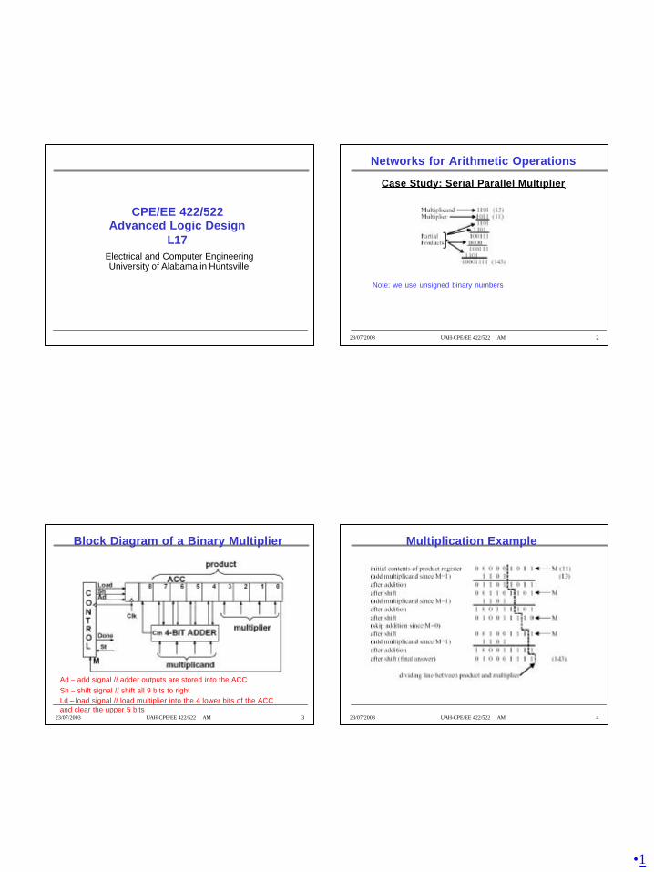
Networks for Arithmetic Operations
Case Study: Serial Parallel Multiplier
Note: we use unsigned binary numbers
23/07/2003 UAH-CPE/EE 422/522 AM 3
Block Diagram of a Binary Multiplier
Ad – add signal // adder outputs are stored into the ACCSh – shift signal // shift all 9 bits to rightLd – load signal // load multiplier into the 4 lower bits of the ACCand clear the upper 5 bits
23/07/2003 UAH-CPE/EE 422/522 AM 4
Multiplication Example

•2
23/07/2003 UAH-CPE/EE 422/522 AM 5
State Graph for Binary Multiplier
23/07/2003 UAH-CPE/EE 422/522 AM 6
Behavioral VHDL Model
23/07/2003 UAH-CPE/EE 422/522 AM 7
Behavioral VHDL Model (cont’d)
23/07/2003 UAH-CPE/EE 422/522 AM 8
Multiplier Control with Counter
• Current design: control part generates the control signals (shift/add) and counts the number of steps
• If the number of bits is large (e.g., 64),the control network can be divided intoa counter and a shift/add control
•3
23/07/2003 UAH-CPE/EE 422/522 AM 9
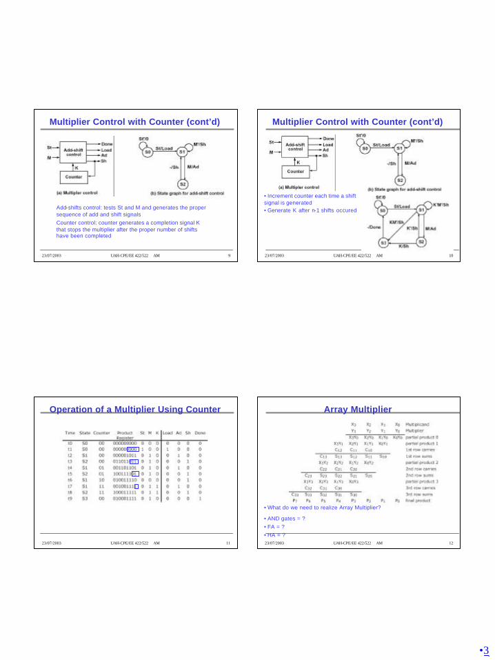
Multiplier Control with Counter (cont’d)
Add-shifts control: tests St and M and generates the proper sequence of add and shift signalsCounter control: counter generates a completion signal K that stops the multiplier after the proper number of shiftshave been completed
23/07/2003 UAH-CPE/EE 422/522 AM 10
Multiplier Control with Counter (cont’d)
• Increment counter each time a shift signal is generated• Generate K after n-1 shifts occured
23/07/2003 UAH-CPE/EE 422/522 AM 11
Operation of a Multiplier Using Counter
23/07/2003 UAH-CPE/EE 422/522 AM 12
Array Multiplier
• What do we need to realize Array Multiplier?
• AND gates = ?• FA = ?• HA = ?
•4
23/07/2003 UAH-CPE/EE 422/522 AM 13
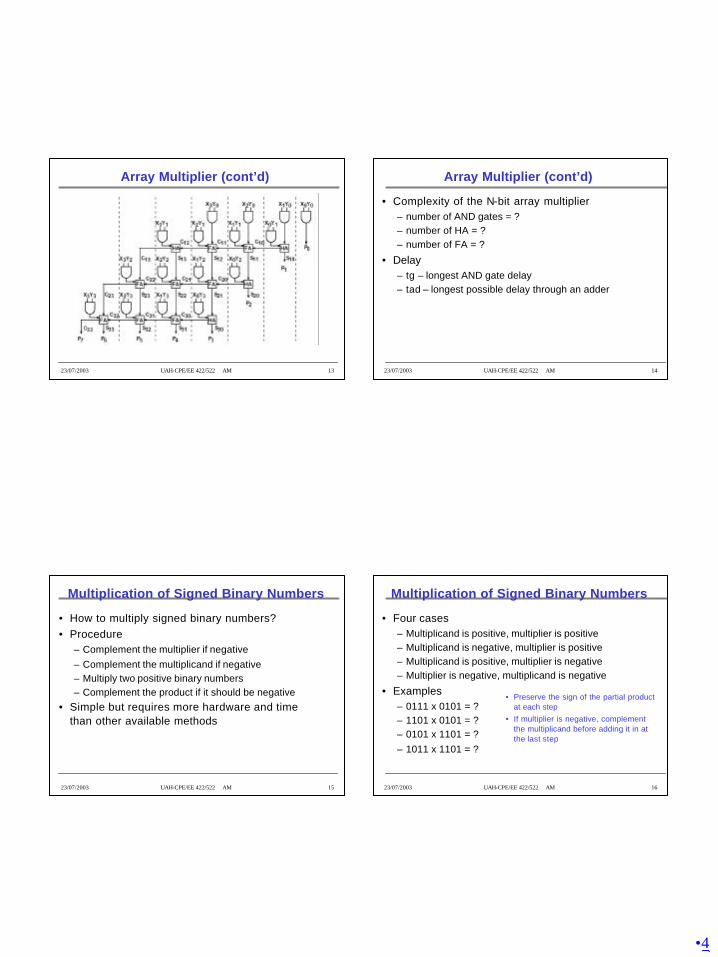
Array Multiplier (cont’d)
23/07/2003 UAH-CPE/EE 422/522 AM 14
Array Multiplier (cont’d)
• Complexity of the N-bit array multiplier– number of AND gates = ?– number of HA = ?– number of FA = ?
• Delay– tg – longest AND gate delay– tad – longest possible delay through an adder
23/07/2003 UAH-CPE/EE 422/522 AM 15
Multiplication of Signed Binary Numbers
• How to multiply signed binary numbers?• Procedure
– Complement the multiplier if negative– Complement the multiplicand if negative– Multiply two positive binary numbers– Complement the product if it should be negative
• Simple but requires more hardware and timethan other available methods
23/07/2003 UAH-CPE/EE 422/522 AM 16
Multiplication of Signed Binary Numbers
• Four cases– Multiplicand is positive, multiplier is positive– Multiplicand is negative, multiplier is positive– Multiplicand is positive, multiplier is negative– Multiplier is negative, multiplicand is negative
• Examples– 0111 x 0101 = ?– 1101 x 0101 = ?– 0101 x 1101 = ?– 1011 x 1101 = ?
• Preserve the sign of the partial product at each step
• If multiplier is negative, complement the multiplicand before adding it in at the last step
•5
23/07/2003 UAH-CPE/EE 422/522 AM 17
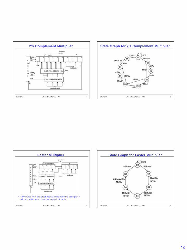
2’s Complement Multiplier
23/07/2003 UAH-CPE/EE 422/522 AM 18
State Graph for 2’s Complement Multiplier
23/07/2003 UAH-CPE/EE 422/522 AM 19
Faster Multiplier
• Move wires from the adder outputs one position to the right =>add and shift can occur at the same clock cycle
23/07/2003 UAH-CPE/EE 422/522 AM 20
State Graph for Faster Multiplier

•6
23/07/2003 UAH-CPE/EE 422/522 AM 21
Behavioral Model for Faster Multiplier
23/07/2003 UAH-CPE/EE 422/522 AM 22
Behavioral Model for Faster Multiplier
23/07/2003 UAH-CPE/EE 422/522 AM 23
Command File and Simulation
23/07/2003 UAH-CPE/EE 422/522 AM 24
Test Bench for Signed Multiplier
•7
23/07/2003 UAH-CPE/EE 422/522 AM 25
Hardware Testing and Design for Testability
• Testing during design process– use VHDL test benches to verify that
the overall design and algorithms used are correct– verify timing and logic after the synthesis
• Post-fabrication testing– when a digital system is manufactured,
test to verify that it is free from manufacturing defects– today, cost of testing is major component of the
manufacturing cost– efficient techniques are needed to test and
design digital systems so that they are easy to test
23/07/2003 UAH-CPE/EE 422/522 AM 26
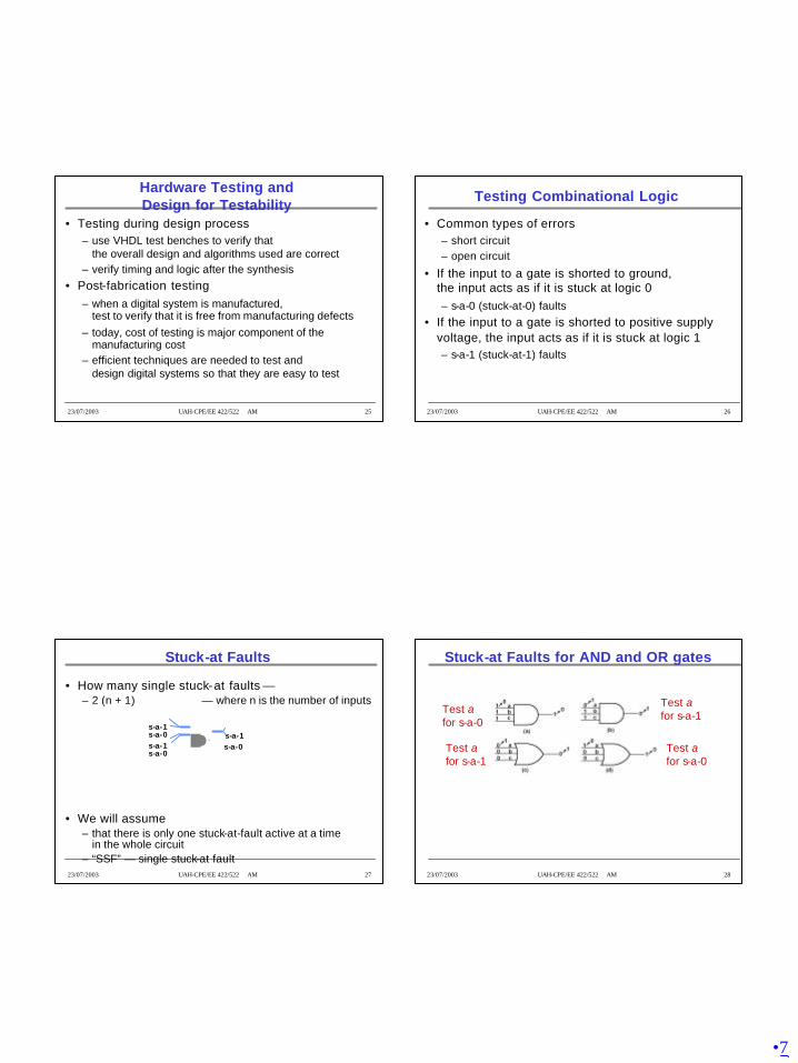
Testing Combinational Logic
• Common types of errors– short circuit– open circuit
• If the input to a gate is shorted to ground,the input acts as if it is stuck at logic 0– s-a-0 (stuck-at-0) faults
• If the input to a gate is shorted to positive supply voltage, the input acts as if it is stuck at logic 1– s-a-1 (stuck-at-1) faults
23/07/2003 UAH-CPE/EE 422/522 AM 27
Stuck-at Faults
• How many single stuck-at faults —– 2 (n + 1) — where n is the number of inputs
• We will assume – that there is only one stuck-at-fault active at a time
in the whole circuit– “SSF” — single stuck-at fault
s-a-0
s-a-0
s-a-0s-a-1
s-a-1s-a-1
23/07/2003 UAH-CPE/EE 422/522 AM 28
Stuck-at Faults for AND and OR gates
Test afor s-a-0
Test afor s-a-1
Test afor s-a-1
Test afor s-a-0

•8
23/07/2003 UAH-CPE/EE 422/522 AM 29
Testing an AND-OR Network
BRUTE-FORCE testing:apply 29=512 different input combinations and check the output
23/07/2003 UAH-CPE/EE 422/522 AM 30
Path Detection & Sensitization: Small Example
Test n to s-a-1
We can test a, m, n, or p to s-a-0
n=0 =>m=0, c = 0 =>a=0, b=1, c=0
d=1, e=0
Change a to 1 =>
Testing internal faults: choose a set of inputs that will excite the fault andthen propagate the fault to the network output
23/07/2003 UAH-CPE/EE 422/522 AM 31
An Example
• What is a minimum set of test vectors to test the network below for all stuck-at-1 and stuck-at-0 faults?
• E.g., start with A-a-p- v-f-F path, determine the test vector to test s-a- 0• determine the list of faults covered• select an untested fault, determine the required ABCD inputs• determine the additional faults tested• repeat the process until all faults are covered
23/07/2003 UAH-CPE/EE 422/522 AM 32
An Example (cont’d)
• Step 1: A- a-p- v-f-F, s-a-0– ABCD: 1101 (+)
• Step 2: s-a- 0 for c– C=1, p=0, w=1 => ABCD=1011 (*)
• Step 3: s-a- 0 for q– C=1, D=1, t=0, s=1 => ABCD=1111 (#)
• Step 4: s-a- 1 for a– A=0, B=1, C=0, D=1 => ABCD=0101 (&)
• Step 5: s-a- 1 for d (%)– D=0, C =0, t=1 => ABCD = 1100
#+f
#+w
&+v
#+u
#*t
*#s
#+r
+#q
*+p
%+d
&*c
*+b
&+a
10
•9
23/07/2003 UAH-CPE/EE 422/522 AM 33
Testing Sequential Logic
• In general, much more difficult than testing combinational logic since we must use sequences of inputs– typically we can observe inputs and outputs,
not the state of flip-flops– assume the reset input,
so we can reset the network to the initial state
• Test procedure– reset the network to the initial state– apply a test sequence and observe the output sequence– if the output is correct, repeat the test for another sequence
• How many test sequences do we have?– how do we test that the initial state of the network under test is
equivalent to the initial state of the correct network?– what is the sequence length?
23/07/2003 UAH-CPE/EE 422/522 AM 34
Testing Sequential Logic (cont’d)
• In practice, if the network has N or fewer states, then apply only input sequences of length less than or equal 2N-1
• Example– consider a network which
includes 5 inputs, 1 output, and 4 states
– total number of test sequences: (25)7 = 235 => infeasible (!)
– derive a small set of test sequences that will adequately test a SN
23/07/2003 UAH-CPE/EE 422/522 AM 35
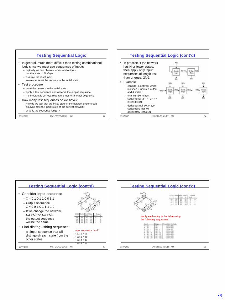
Testing Sequential Logic (cont’d)
• Consider input sequence– X = 0 1 0 1 1 0 0 1 1– Output sequence
Z = 0 0 1 0 1 1 1 1 0– If we change the network
S3->S0 => S3->S3,the output sequence will be the same
• Find distinguishing sequence – an input sequence that will
distinguish each state from the other states
Input sequence: X=11• S0: Z = 01• S1: Z = 11• S2: Z = 10• S3: Z = 00
23/07/2003 UAH-CPE/EE 422/522 AM 36
Testing Sequential Logic (cont’d)
Verify each entry in the table using the following sequences:

•10
23/07/2003 UAH-CPE/EE 422/522 AM 37
Testing Sequential Logic (cont’d)
• Implementation of the FSM– S0=00, S1=10, S2=01, S3=11
• Test a for s-a-1– to do this Q1Q2 must be 10
=> go to the state S1 and then set X to 0 (R10)
– in normal operation, the next state will be S0;if a is s-a- 1 then next state is S2
– distinguish the state (S0 or S2);apply sequence 11
– Final sequence: R1011Normal output: 0101Faulty output: 0110
23/07/2003 UAH-CPE/EE 422/522 AM 38
Scan Testing
• Testing of sequential networks is greatly simplified if we can observe the state of all the flip-flops instead of just observing the network outputs– Connect the output of each flip-flop to one of the IC
pins?– Arrange flip-flops to form a shift register =>
shift out the state of flip-flops bit by bit using a single serial output pin => Scan path testing
23/07/2003 UAH-CPE/EE 422/522 AM 39
Scan Path Testing
• Sequential network is separated into a combinational logic part and a state register composed of flip-flops
• Two ports FFs (2 D inputs and 2 clock inputs)
– D1 is stored in the FF on C1 pulse– D2 is stored in the FF on C2 pulse– Q of each FF is connected to D2 of the next FF to form a shift register
23/07/2003 UAH-CPE/EE 422/522 AM 40
Scan Path Testing
• Normal operation– system clock SCK = C1– inputs: X1 X2...XN
– outputs: Z1Z2...ZN
• Testing– FFs are set to a specified
state using the SDI and TCK– test vector is applied
X1X2...XN
– outputs Z1Z2...ZN are verified– SCK is pulsed to take the
network to the next state– next state is verified by
pulsing the TCK to shift the state code out of the scan register via SDO

•11
23/07/2003 UAH-CPE/EE 422/522 AM 41
Scan Path Testing: An Example
• SQ: X1X2, Q1Q2Q3, Z1Z2
23/07/2003 UAH-CPE/EE 422/522 AM 42
Scan Chain
23/07/2003 UAH-CPE/EE 422/522 AM 43
Scan Test with Multiple ICs
23/07/2003 UAH-CPE/EE 422/522 AM 44
Boundary Scan
• PCB testing has become more difficult– ICs have become more complex, with more and more pins – PCBs have become more denser with multiple layers and fine traces– Bed-of-nails testing
• use sharp probes to contact the traces on the board• test data are applied to and read from various ICs • => not practical for high -density PCBs with fine traces and complex ICs
• Boundary scan test methodology:introduced to facilitate the testing of complex PC boards– developed by JTAG (Joint Task Action Group) – adopted as ANSI/IEEE Standard 1149.1 –
“Standard Test Access Port and Boundary Scan Architecture”– IC manufacturers make ICs that conform the standard– ICs can be linked together on a PCB, so that they can be tested
using only a few pins on the PCB edge connector
•12
23/07/2003 UAH-CPE/EE 422/522 AM 45
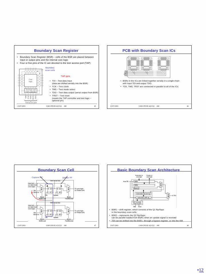
Boundary Scan Register
• Boundary Scan Register (BSR) – cells of the BSR are placed between input or output pins and the internal core logic
• Four or five pins of the IC are devoted to the test- access-port (TAP)
TAP pins
Boundary scan cells
• TDI – Test data input (data are shifted serially into the BSR)
• TCK – Test clock• TMS – Test mode select
• TDO – Test data output (serial output from BSR)
• TRST – Test reset (resets the TAP controller and test logic –optional pin)
23/07/2003 UAH-CPE/EE 422/522 AM 46
PCB with Boundary Scan ICs
• BSRs in the ICs are linked together serially in a single chain with input TDI and output TDO.
• TCK, TMS, TRST are connected in parallel to all of the ICs.
23/07/2003 UAH-CPE/EE 422/522 AM 47
Boundary Scan Cell
Capture FF Update FF
23/07/2003 UAH-CPE/EE 422/522 AM 48
Basic Boundary Scan Architecture
• BSR1 – shift register, which consists of the Q1 flip-flops in the boundary scan cells
• BSR2 – represents the Q2 flip-flops; can be parallel loaded from BSR1 when an update signal is received
• TDI can be shifted into the BSR1, through a bypass register, or into the ISR
•13
23/07/2003 UAH-CPE/EE 422/522 AM 49
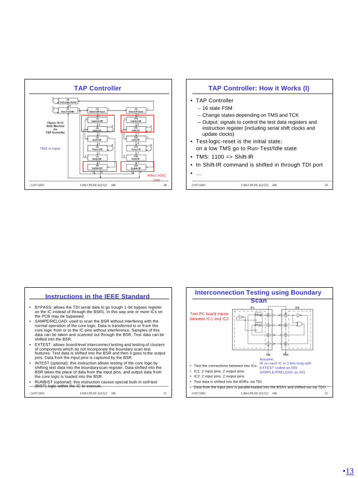
TAP Controller
TMS is input
Affect ASIC core
23/07/2003 UAH-CPE/EE 422/522 AM 50
TAP Controller: How it Works (I)
• TAP Controller – 16 state FSM – Change states depending on TMS and TCK– Output: signals to control the test data registers and
instruction register (including serial shift clocks and update clocks)
• Test-logic-reset is the initial state; on a low TMS go to Run-Test/Idle state
• TMS: 1100 => Shift- IR • In Shift-IR command is shifted in through TDI port
• …
23/07/2003 UAH-CPE/EE 422/522 AM 51
Instructions in the IEEE Standard
• BYPASS: allows the TDI serial data to go trough 1- bit bypass register on the IC instead of through the BSR1. In this way one or more ICs on the PCB may be bypassed.
• SAMPE/RELOAD: used to scan the BSR without interfering with the normal operation of the core logic. Data is transferred to or fr om the core logic from or to the IC pins without interference. Samples of this data can be taken and scanned out through the BSR. Test data can be shifted into the BSR.
• EXTEST: allows board-level interconnect testing and testing of clusters of components which do not incorporate the boundary scan test features. Test data is shifted into the BSR and then it goes to the output pins. Data from the input pins is captured by the BSR.
• INTEST (optional): this instruction allows testing of the core logic by shifting test data into the boundary-scan register. Data shifted into the BSR takes the place of data from the input pins, and output data from the core logic is loaded into the BSR.
• RUNBIST (optional): this instruction causes special built-in self-test (BIST) logic within the IC to execute.
23/07/2003 UAH-CPE/EE 422/522 AM 52
Interconnection Testing using Boundary Scan
• Test the connections between two ICs.
• IC1: 2 input pins, 2 output pins.• IC2: 2 input pins, 2 output pins.
• Test data is shifted into the BSRs via TDI.
• Data from the input pins is parallel-loaded into the BSRs and shifted out via TDO.
Assume:IR on each IC is 3 bits long with EXTEST coded as 000SAMPLE/PRELOAD as 001
Test PC board traces between IC1 and IC2
•14
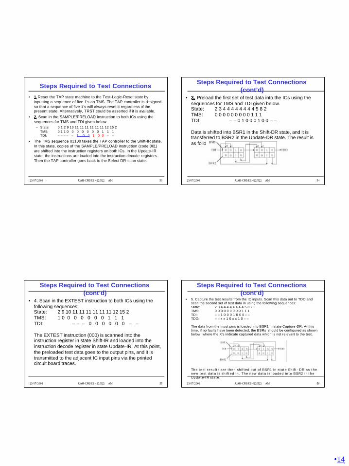
23/07/2003 UAH-CPE/EE 422/522 AM 53
Steps Required to Test Connections
• 1. Reset the TAP state machine to the Test-Logic-Reset state by inputting a sequence of five 1's on TMS. The TAP controller is designed so that a sequence of five 1's will always reset it regardless of the present state. Alternatively, TRST could be asserted if it is available.
• 2. Scan in the SAMPLE/PRELOAD instruction to both ICs using the sequences for TMS and TDI given below.
– State: 0 1 2 9 10 11 11 11 11 11 11 12 15 2TMS: 0 1 1 0 0 0 0 0 0 0 1 1 1TDI: – – – – – 1 0 0 1 0 0 – –
• The TMS sequence 01100 takes the TAP controller to the Shift-IR state. In this state, copies of the SAMPLE/PRELOAD instruction (code 001) are shifted into the instruction registers on both ICs. In the U pdate-IR state, the instructions are loaded into the instruction decode registers. Then the TAP controller goes back to the Select DR-scan state.
23/07/2003 UAH-CPE/EE 422/522 AM 54
Steps Required to Test Connections (cont’d)
• 3. Preload the first set of test data into the ICs using the sequences for TMS and TDI given below.State: 2 3 4 4 4 4 4 4 4 4 5 8 2TMS: 0 0 0 0 0 0 0 0 0 1 1 1TDI: – – 0 1 0 0 0 1 0 0 – –
Data is shifted into BSR1 in the Shift-DR state, and it is transferred to BSR2 in the Update-DR state. The result is as follows:
23/07/2003 UAH-CPE/EE 422/522 AM 55
Steps Required to Test Connections (cont’d)
• 4. Scan in the EXTEST instruction to both ICs using the following sequences:State: 2 9 10 11 11 11 11 11 11 12 15 2TMS: 1 0 0 0 0 0 0 0 1 1 1TDI: – – – 0 0 0 0 0 0 – –
The EXTEST instruction (000) is scanned into the instruction register in state Shift-IR and loaded into the instruction decode register in state Update-IR. At this point, the preloaded test data goes to the output pins, and it is transmitted to the adjacent IC input pins via the printed circuit board traces.
23/07/2003 UAH-CPE/EE 422/522 AM 56
Steps Required to Test Connections (cont’d)
• 5. Capture the test results from the IC inputs. Scan this data out to TDO and scan the second set of test data in using the following sequences:State: 2 3 4 4 4 4 4 4 4 4 5 8 2TMS: 0 0 0 0 0 0 0 0 0 1 1 1TDI: – – 1 0 0 0 1 0 0 0 – –TDO: – – x x 1 0 x x 1 0 – –
The data from the input pins is loaded into BSR1 in state Capture -DR. At this time, if no faults have been detected, the BSRs should be configured as shown below, where the X's indicate captured data which is not relevant to the test.
The test results are then shifted out of BSR1 in state Shift -DR as the new test data is shifted in. The new data is loaded into BSR2 in the Update-IR state.
•15
23/07/2003 UAH-CPE/EE 422/522 AM 57
Steps Required to Test Connections (cont’d)
• 6. Capture the test results from the IC inputs. Scan this data out to TDO and scan all 0's in using the following sequences:State: 2 3 4 4 4 4 4 4 4 4 5 8 2 9 0TMS: 0 0 0 0 0 0 0 0 0 1 1 1 1 1TDI: – – 0 0 0 0 0 0 0 0 – – – –TDO: – – x x 0 1 x x 0 1 – – – –
The data from the input pins is loaded into BSR1 in state Capture-DR. Then it is shifted out in state Shift-DR as all 0's are shifted in. The 0's are loaded into BSR2 in the Update-IR state. The controller then returns to the Test-Logic-Reset state and normal operation of the ICs can then occur. The interconnection test passes if the observed TDO sequences match the ones given above.
23/07/2003 UAH-CPE/EE 422/522 AM 58
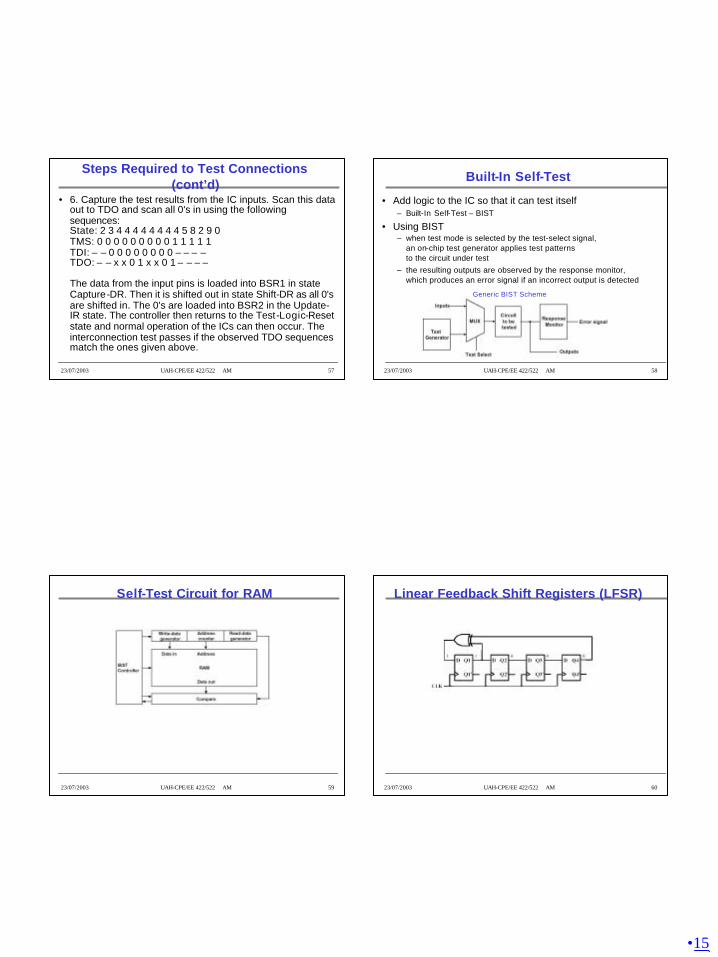
Built-In Self-Test
• Add logic to the IC so that it can test itself– Built-In Self-Test – BIST
• Using BIST– when test mode is selected by the test-select signal,
an on-chip test generator applies test patterns to the circuit under test
– the resulting outputs are observed by the response monitor,which produces an error signal if an incorrect output is detected
Generic BIST Scheme
23/07/2003 UAH-CPE/EE 422/522 AM 59
Self-Test Circuit for RAM
23/07/2003 UAH-CPE/EE 422/522 AM 60
Linear Feedback Shift Registers (LFSR)

•16
23/07/2003 UAH-CPE/EE 422/522 AM 61
Self-Test Circuit for RAM with Signature Regs
MISR – Multiple Input Signature Register
E.g. for MISR –form a check-sum by adding up all data bytes stored in the RAM