near-field radiative heat transfer between doped-si
TRANSCRIPT

Near-field radiative heat transfer between doped-Si parallel plates separated by aspacing down to 200 nmJesse I. Watjen, Bo Zhao, and Zhuomin M. Zhang Citation: Applied Physics Letters 109, 203112 (2016); doi: 10.1063/1.4967384 View online: http://dx.doi.org/10.1063/1.4967384 View Table of Contents: http://scitation.aip.org/content/aip/journal/apl/109/20?ver=pdfcov Published by the AIP Publishing Articles you may be interested in Electrically tunable near-field radiative heat transfer via ferroelectric materials Appl. Phys. Lett. 105, 244102 (2014); 10.1063/1.4904456 Graphene-assisted near-field radiative heat transfer between corrugated polar materials Appl. Phys. Lett. 104, 251911 (2014); 10.1063/1.4885396 Near-field radiative heat transfer between doped silicon nanowire arrays Appl. Phys. Lett. 102, 053101 (2013); 10.1063/1.4790143 Near-field radiative transfer based thermal rectification using doped silicon Appl. Phys. Lett. 98, 113106 (2011); 10.1063/1.3567026 Radiative heat transfer at nanoscale mediated by surface plasmons for highly doped silicon Appl. Phys. Lett. 95, 231913 (2009); 10.1063/1.3271681
Reuse of AIP Publishing content is subject to the terms at: https://publishing.aip.org/authors/rights-and-permissions. Download to IP: 143.215.88.230 On: Tue, 15 Nov 2016
19:07:02

Near-field radiative heat transfer between doped-Si parallel plates separatedby a spacing down to 200 nm
Jesse I. Watjen,a) Bo Zhao,a) and Zhuomin M. Zhangb)
George W. Woodruff School of Mechanical Engineering, Georgia Institute of Technology, Atlanta,Georgia 30332, USA
(Received 4 July 2016; accepted 27 October 2016; published online 15 November 2016)
Heat transfer between two objects separated by a nanoscale vacuum gap holds great promise
especially in energy harvesting applications such as near-field thermophotovoltaic systems.
However, experimental validation of nanoscale radiative heat transfer has been largely limited to
tip-plate configurations due to challenges of maintaining small gap spacing over a relatively large
area. Here, we report measurements of heat transfer near room temperature between two 1 cm by
1 cm doped-Si parallel plates, separated by a vacuum gap from about 200 nm to 780 nm. The mea-
sured strong near-field radiative transfer is in quantitative agreement with the theoretical prediction
based on fluctuational electrodynamics. The largest measured radiative heat flux is 11 times as high
as the blackbody limit for the same hot and cold surface temperatures. Our experiments have pro-
duced the highest radiative heat transfer rate observed to date across submicron distances between
objects near room temperature. Published by AIP Publishing.[http://dx.doi.org/10.1063/1.4967384]
The increasing demand for sustainable energy leads to
an urgent need for alternative energy harvesting methods
with better performance than current technologies. Near-
field radiative heat transfer is one of the most promising
routes for boosting the efficiency and power output of energy
harvesting systems such as thermophotovoltaics.1 It has been
shown that when two objects at different temperatures are
brought within a distance much smaller than the characteris-
tic wavelength of thermal radiation, the radiative heat flux
can exceed the well-known blackbody limit governed by the
Stefan-Boltzmann law by orders of magnitude.2–4 This effect
is caused by the coupling of forward and backward evanes-
cent waves that opens the paths for photons to tunnel from
the hot side to the cold side. Theoretically, near-field radia-
tive heat flux scales up with d2, where d is the gap spacing
between two parallel plates.2,5 For energy harvesting appli-
cations, increasing the surface area and shrinking the gap
spacing are both critical in order to achieve high radiative
heating rates. While tremendous progress has been made in
recent years toward experimental realization, measurements
between planar surfaces with square-centimeter-sized areas
at deep submicron gap distances are still quite challenging
due to difficulties in controlling the gap spacing.6 In this
work, we experimentally measured the radiative heat transfer
between two 1-cm2 doped-Si plates separated by a vacuum
gap spacing from (782 6 40) nm down to (200 6 80) nm.
With careful control, thermal radiation dominates the heat
transfer and the design may be extended to even larger heat
transfer areas with other materials and thus may be imple-
mented in applications such as near-field thermophotovol-
taics,1,7 thermal rectification,8,9 thermal transistors,10 and
radiative refrigeration.11,12
Using complicated experiments enabled by scanning
probe microscopy (SPM), researchers have measured the
near-field radiative heat transfer between an SPM tip (or a
small sphere) and a flat surface at gap distances down to tens
of or even a few nanometers.3,4,13–17 However, this type of
configuration has a relatively small area where photon tunnel-
ing may occur and thus the heating rate is extremely limited,
preventing it for use in applications that require a large photon
flux. Continuous efforts have been made to overcome this lim-
itation by measuring near-field thermal radiation between pla-
nar (or flat) surfaces, and significant progress has been made
in recent years.18–26 For example, Ito et al.24 measured the
near-field heat flux between two fused quartz substrates, with
an area of 1.6 cm2, at gap spacings down to 500 nm. In the
study by St-Gelais et al.,25 a gap spacing near 40 nm was
reached but the surface area was much smaller. Very recently,
Song et al.26 developed a microdevice that can achieve a spac-
ing down to about 100 nm with surface areas about 50 lm by
50 lm. However, most of the reported experiments are still
limited by either small heat transfer areas or relatively large
gap spacings. These limitations can be understood if we con-
sider that, for a perfectly flat 1-cm-wide piece to achieve
100 nm gap spacing, the angle of the piece cannot be off by
more than 6 104 deg. Otherwise, contact between the two
plates would occur at the end, and consequently, conduction
would dominate the heat transfer. If the non-flatness of the
sample surface is also considered, it is almost impossible to
maintain a perfect nanometric gap over large areas. Therefore,
there naturally exists a tradeoff between the surface area
and the parallelism of the gap in practice. In order to benefit
the real-world applications using near-field thermal radiation,
it is imperative to explore a practical design that can reveal
the near-field effect by keeping stringent parallelism between
two planar surfaces with a relatively large heat transfer area
and that can potentially be scaled up without too much
complexity.
a)J. I. Watjen and B. Zhao contributed equally to this work.b)Author to whom correspondence should be addressed. Electronic mail:
0003-6951/2016/109(20)/203112/5/$30.00 Published by AIP Publishing.109, 203112-1
APPLIED PHYSICS LETTERS 109, 203112 (2016)
Reuse of AIP Publishing content is subject to the terms at: https://publishing.aip.org/authors/rights-and-permissions. Download to IP: 143.215.88.230 On: Tue, 15 Nov 2016
19:07:02

An experimental platform was developed in the present
work for measuring the near-field heat transfer, as shown in
Fig. 1(a). The spring presses the stack of layers onto a copper
base to form a nearly one-dimensional heat flow path. The
lateral dimensions of these layers, as well as the raised base
plate, are 1 cm by 1 cm. On top of the stack lays a printed
resistance heater (in red color online). A DC power supply
provides 10–300 mW to the resistance heater. The heater is
epoxied to a 1-mm-thick copper plate (in orange) that is gold
plated to reduce the radiative heat loss. The sample (in blue)
is sandwiched between two identical copper plates using a
thin layer of silver grease to ensure good thermal contact. A
tiny hole drilled halfway through the side allows a thermo-
couple to be inserted on each copper plate to measure the
hot-side and cold-side temperatures of the sample, T1 and T2,
respectively. The applied power generates a temperature dif-
ference (DT1 ¼ T1 T2) about 2–30 K between the copper
plates. A thermopile-type heat flux meter (HFM) is epoxied
underneath the lower copper plate and atop the raised base
plate. A calibrated silicon diode thermistor mounted on the
base plate measures the absolute temperature of the heat sink
(T0) with an uncertainty of 37 mK. The base plate is screw-
fastened to the inside of a vacuum chamber. A thermocouple
constructed using nickel-chromium (blue) and constantan
(red) wires measures the temperature difference, DT2 ¼ T2
T0, in order to determine the cold plate temperature T2,
while the other measures the temperature difference between
the copper plates DT1 to obtain the absolute temperature T1.
Aluminum foil (not shown) surrounded the sample stage
serves as a radiation shield to reduce the side heat loss.
Together with the heat flux measured, the thermal conduc-
tance of the sample can be quantified and compared with the-
oretical predictions. A spring on top of the stack applies a
quantifiable force on the sample.
The samples were constructed with two square pieces of
doped-Si fabricated from double-side-polished wafers. The
upper piece closer to the heater is called the radiation emitter
while the lower piece is called the receiver throughout this
paper. To create a desired gap spacing between the pieces, a
two-dimensional array of SiO2 posts was fabricated on one
piece using ultraviolet photolithography, as shown in Fig. 1(b).
SiO2 was chosen because of its low thermal conductivity, high
mechanical strength, and ease of fabrication. The height of the
posts varies between samples and ranges from 200 nm to
800 nm. An unpatterned piece was then mated together with
the patterned piece in a cleanroom environment to form a sub-
micron gap. The gap spacing is controlled by the height of
posts and the applied force. Extremely flat wafers with a thick-
ness approximately 500 lm were employed, and a silicon diox-
ide layer was deposited on the back side of some wafers for
bow reduction. The detailed fabrication process is described in
the supplementary material. Since the typical size of dust par-
ticles is on the order of micrometers, the small gap spacing nat-
urally prevents particulate matter from entering the gap. While
the posts maintain mechanical stability of the gap, they also
introduce additional pathways for heat to conduct from the
emitter to the receiver.
To measure the radiative heat transfer, it is preferred to
ensure that thermal radiation is the dominant transfer mode
across the sample. Note that the effect of gas conduction is
eliminated by maintaining the pressure in the chamber below
3 104 Pa. Although near-field radiative transfer increases
considerably as gap spacings approach the nanometer range,
it is still orders of magnitude weaker compared to conduction
heat transfer with the same cross-sectional area. Therefore,
the number of the posts should be reduced as much as possi-
ble while maintaining the gap spacing mechanically. A pho-
tomask was made that contains four patterns with different
spans between posts, i.e., S equals to 200 lm, 300 lm,
400 lm, and 500 lm. With a post diameter of approximately
1 lm, it is estimated that more than half of the conductance
is due to radiation when S exceeds about 300 lm (see supple-
mentary material for details).
Even though the thermal grease was applied, contact
resistance could not be completely removed. Thus, after
measuring the samples under vacuum, the chamber was
returned to ambient pressure where gas conduction across
the gap dominates and the thermal resistance of the sample
is negligible due to the large thermal conductivity of silicon.
Thermal resistances of the Cu plates are also negligible.
Thus, the contact resistance at the copper-silicon interfaces
can be obtained based on the measured T1 and T2 when the
chamber is at ambient pressure. It is assumed that the contact
resistance is the same above and below the sample. The con-
tact resistance value, ranging from 4 to 9 K/W across each
Si-Cu interface, was used to deduce the temperatures of the
two Si pieces, i.e., the emitter (TH) and receiver (TL). The
radiative heat transfer rate, qrad, is obtained by excluding
the conduction from the total heat transfer rate measured
by the heat flux meter with the assumption that all posts have
the same height as the gap spacing. The radiative heat trans-
fer coefficient is calculated from
hrad ¼qrad=A
DT; (1)
where the area A¼ 1 cm2, by neglecting the posts, and DT¼ TH TL.
Figure 2 displays qrad for three different gap spacings ver-
sus DT. The isolated solid symbols represent the measured
results with uncertainty bounds indicated by the error bars.
FIG. 1. Schematics of the experimental setup for measuring the near-field radi-
ative heat transfer between flat plates and the structure of the sample. (a) The
measurement stage that contains a stack of layers below the spring, namely, a
heater, the upper Cu plate, the sample made of two doped-Si plates separated
by a gap, the lower Cu plate, and a heat flux meter (HFM) mounted on a Cu
heat sink. (b) The sample made of two doped-Si pieces separated by a submi-
cron gap using SiO2 posts, where S is the distance between adjacent posts.
203112-2 Watjen, Zhao, and Zhang Appl. Phys. Lett. 109, 203112 (2016)
Reuse of AIP Publishing content is subject to the terms at: https://publishing.aip.org/authors/rights-and-permissions. Download to IP: 143.215.88.230 On: Tue, 15 Nov 2016
19:07:02
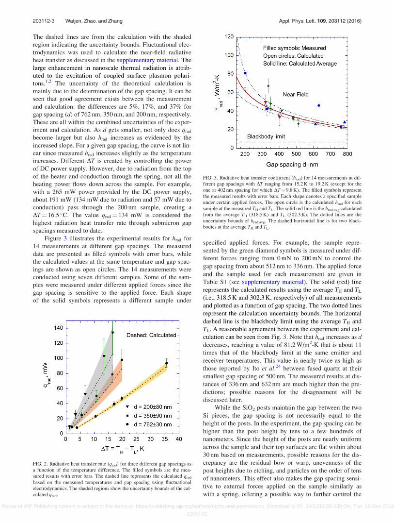
The dashed lines are from the calculation with the shaded
region indicating the uncertainty bounds. Fluctuational elec-
trodynamics was used to calculate the near-field radiative
heat transfer as discussed in the supplementary material. The
large enhancement in nanoscale thermal radiation is attrib-
uted to the excitation of coupled surface plasmon polari-
tons.1,2 The uncertainty of the theoretical calculation is
mainly due to the determination of the gap spacing. It can be
seen that good agreement exists between the measurement
and calculation: the differences are 5%, 17%, and 37% for
gap spacing (d) of 762 nm, 350 nm, and 200 nm, respectively.
These are all within the combined uncertainties of the exper-
iment and calculation. As d gets smaller, not only does qrad
become larger but also hrad increases as evidenced by the
increased slope. For a given gap spacing, the curve is not lin-
ear since measured hrad increases slightly as the temperature
increases. Different DT is created by controlling the power
of DC power supply. However, due to radiation from the top
of the heater and conduction through the spring, not all the
heating power flows down across the sample. For example,
with a 265 mW power provided by the DC power supply,
about 191 mW (134 mW due to radiation and 57 mW due to
conduction) pass through the 200 nm sample, creating a
DT¼ 16.5 C. The value qrad¼ 134 mW is considered the
highest radiation heat transfer rate through submicron gap
spacings measured to date.
Figure 3 illustrates the experimental results for hrad for
14 measurements at different gap spacings. The measured
data are presented as filled symbols with error bars, while
the calculated values at the same temperature and gap spac-
ings are shown as open circles. The 14 measurements were
conducted using seven different samples. Some of the sam-
ples were measured under different applied forces since the
gap spacing is sensitive to the applied force. Each shape
of the solid symbols represents a different sample under
specified applied forces. For example, the sample repre-
sented by the green diamond symbols is measured under dif-
ferent forces ranging from 0 mN to 200 mN to control the
gap spacing from about 512 nm to 336 nm. The applied force
and the sample used for each measurement are given in
Table S1 (see supplementary material). The solid (red) line
represents the calculated results using the average TH and TL
(i.e., 318.5 K and 302.3 K, respectively) of all measurements
and plotted as a function of gap spacing. The two dotted lines
represent the calculation uncertainty bounds. The horizontal
dashed line is the blackbody limit using the average TH and
TL. A reasonable agreement between the experiment and cal-
culation can be seen from Fig. 3. Note that hrad increases as ddecreases, reaching a value of 81.2 W/m2-K that is about 11
times that of the blackbody limit at the same emitter and
receiver temperatures. This value is nearly twice as high as
those reported by Ito et al.24 between fused quartz at their
smallest gap spacing of 500 nm. The measured results at dis-
tances of 336 nm and 632 nm are much higher than the pre-
dictions; possible reasons for the disagreement will be
discussed later.
While the SiO2 posts maintain the gap between the two
Si pieces, the gap spacing is not necessarily equal to the
height of the posts. In the experiment, the gap spacing can be
higher than the post height by tens to a few hundreds of
nanometers. Since the height of the posts are nearly uniform
across the sample and their top surfaces are flat within about
30 nm based on measurements, possible reasons for the dis-
crepancy are the residual bow or warp, unevenness of the
post heights due to etching, and particles on the order of tens
of nanometers. This effect also makes the gap spacing sensi-
tive to external forces applied on the sample similarly as
with a spring, offering a possible way to further control the
FIG. 2. Radiative heat transfer rate (qrad) for three different gap spacings as
a function of the temperature difference. The filled symbols are the mea-
sured results with error bars. The dashed line represents the calculated qrad
based on the measured temperatures and gap spacing using fluctuational
electrodynamics. The shaded regions show the uncertainty bounds of the cal-
culated qrad.
FIG. 3. Radiative heat transfer coefficient (hrad) for 14 measurements at dif-
ferent gap spacings with DT ranging from 15.2 K to 19.2 K (except for the
one at 402 nm spacing for which DT¼ 9.8 K). The filled symbols represent
the measured results with error bars. Each shape denotes a specified sample
under certain applied forces. The open circle is the calculated hrad for each
sample at the measured TH and TL. The solid red line is the hrad,avg calculated
from the average TH (318.5 K) and TL (302.3 K). The dotted lines are the
uncertainty bounds of hrad,avg. The dashed horizontal line is for two black-
bodies at the average TH and TL.
203112-3 Watjen, Zhao, and Zhang Appl. Phys. Lett. 109, 203112 (2016)
Reuse of AIP Publishing content is subject to the terms at: https://publishing.aip.org/authors/rights-and-permissions. Download to IP: 143.215.88.230 On: Tue, 15 Nov 2016
19:07:02

gap spacing through nearly elastic deformation. Therefore,
in the experiment, we used a Fourier-transform infrared
spectrometer (FTIR) to measure the reflectance of each sam-
ple to quantify the gap spacing prior to the heat transfer mea-
surement. In some more recent measurements, different
forces were applied for both the FTIR measurement and the
heat transfer measurement, allowing the gap spacing to be
adjusted.
As mentioned before, the sample contains two doped-Si
slabs, about 500 lm thickness, sandwiching a thin layer of
vacuum or air. The spectral reflectance depends on the thick-
ness of the middle layer due to interference effects, and thus
the reflectance spectrum can be used to determine the gap
spacing. The reflectance is insensitive to the thickness of the
Si slabs since the FTIR resolution is not high enough to dis-
tinguish the interference fringes in the Si slab, which can be
treated as incoherent.5 This technique, however, requires the
Si slab to be transparent at least in a certain frequency range
for the infrared radiation to penetrate through and generate a
distinguishable interference pattern. Meanwhile, the material
is required to be opaque in the mid- and far-infrared range to
have a considerable radiative heat flux. Calculations suggest
that, for 500-lm-thick Si wafers, a doping concentration
from 1 1018 to 3 1018 cm3 can still be transparent at
wavenumbers from 2 000 cm1 to 10 000 cm1 for FTIR
measurements of the gap spacing, while at the same time can
have sufficient free-carrier absorption at longer wavelengths
for near-field radiative transfer enhancement.27,28 Si wafers
doped with antimony atoms of 2 1018 cm3 concentration
were purchased from a commercial vendor. Their optical
constants are extracted from the measured reflectance and
transmittance of the wafer as well as extended to the mid-
and far-infrared using a Drude model (see supplementary
material). The doped-Si pieces can be treated as semi-infinite
when considering the near-field radiative heat transfer, so
that the backside oxide films and other materials at the con-
tact have negligible effects on the radiative heat transfer.
However, the oxide film does affect the measured FTIR
spectrum as discussed next.
A fixture was manufactured and mounted on the reflectance
accessory of the FTIR in order to apply different forces on the
sample during the reflectance measurement in a similar manner
as shown in Fig. 1(a) for heat transfer measurements.
Considering the yield stresses of the SiO2 and Si, the applied
force on the sample is limited to 200 mN. The gap distance is
determined using a least-squares method by comparing the mea-
sured reflectance spectrum with the theoretical curves at differ-
ent gap spacings. Figure 4 shows the measured and calculated
reflectance spectra for three different gap spacings. The spec-
trum for the sample with 200 nm spacing is different since the
patterned and the unpatterned piece have a silicon dioxide film
of 595 nm and 785 nm, respectively, on the back sides. The gap
spacing is determined such that the predicted spectrum at this
gap spacing yields the smallest standard error of estimate com-
pared to the measurement as discussed in the supplementary
material. After the gap spacing is fully characterized, the sample
is mounted in the experimental setup to measure the thermal
conductance with a force applied to achieve a desired gap spac-
ing. While good agreement between the measurement and cal-
culation is obtained for most data points shown in Fig. 3, it
should be noted that for the sample shown with diamond sym-
bols, the reflectance spectra for 260 nm< d< 340 nm are almost
indistinguishable, which may explain the deviation of the mea-
sured result at 336 nm spacing. A smaller gap spacing than the
prescribed value would increase the calculated hrad and decrease
the measured hrad, making the agreement between them possi-
ble. This can be a limitation of using doped-Si in the current
experiment, but may be alleviated when other materials are
used. Note that the force needs to be applied with great care
since an uneven distribution of forces can cause the sample to
deform nonuniformly and create local bow that makes the gap
spacing smaller than that determined by FTIR. This can cause a
larger measured hrad than the calculated value and could be the
reason for the deviation of measurement at 632 nm spacing.
Because the sample is contaminated by the grease after the ther-
mal conductance measurement, they cannot be remeasured on
the FTIR. The result for the 632 nm spacing is shown to stress
the importance of handling the sample in the experiments.
The experimental results presented here demonstrate
that the near-field effect can be probed with a heat transfer
area at the square-centimeter scale and gap spacings down to
about 200 nm. The high heat transfer rate achieved from this
study may facilitate practical applications in energy conver-
sion and thermal management devices based on near-field
thermal radiation. With the development of this technique
and future improvements, it is expected that accurate meas-
urements can be made possible between various materials
and nanostructures with even larger heat transfer areas that
can potentially yield even stronger near-field heat transfer.
Experiments of this nature and insights from such studies
may signify breakthroughs in applications of near-field ther-
mophotovoltaics, radiative cooling and refrigeration, and
thermal rectifiers or transistors.
See supplementary material for details of sample fabri-
cation, dielectric function, gap spacing determination, uncer-
tainty analysis, and theoretical calculations.
FIG. 4. Reflectance spectra for three samples with different gap spacings.
The sample with a spacing of 200 nm has an oxide film of 595 nm and
785 nm on the back sides of the patterned and the unpatterned pieces,
respectively.
203112-4 Watjen, Zhao, and Zhang Appl. Phys. Lett. 109, 203112 (2016)
Reuse of AIP Publishing content is subject to the terms at: https://publishing.aip.org/authors/rights-and-permissions. Download to IP: 143.215.88.230 On: Tue, 15 Nov 2016
19:07:02

This work was primarily supported by the U.S.
Department of Energy, Office of Science, Basic Energy
Science (DE-FG02-06ER46343). B.Z. and Z.M.Z. were also
supported by the National Science Foundation (CBET-
1235975; CBET-1603761). The facilities at Georgia Tech’s
Institute for Electronics and Nanotechnology (IEN) were
used for the sample fabrication and some characterizations.
1S. Basu, Y.-B. Chen, and Z. M. Zhang, Int. J. Energy Res. 31, 689 (2007).2C. J. Fu and Z. M. Zhang, Int. J. Heat Mass Transfer 49, 1703 (2006).3S. Shen, A. Narayanaswamy, and G. Chen, Nano Lett. 9, 2909 (2009).4E. Rousseau, A. Siria, G. Jourdan, S. Volz, F. Comin, J. Chevrier, and J.-J.
Greffet, Nat. Photonics 3, 514 (2009).5Z. M. Zhang, Nano/Microscale Heat Transfer (McGraw-Hill, New York,
2007).6X. L. Liu, L. P. Wang, and Z. M. Zhang, Nanoscale Microscale
Thermophys. Eng. 19, 98 (2015).7R. S. DiMatteo, P. Greiff, S. L. Finberg, K. A. Young-Waithe, H. K. H.
Choy, M. M. Masaki, and C. G. Fonstad, Appl. Phys. Lett. 79, 1894
(2001).8C. R. Otey, W. T. Lau, and S. Fan, Phys. Rev. Lett. 104, 154301 (2010).9L. P. Wang and Z. M. Zhang, Nanoscale Microscale Thermophys. Eng.
17, 337 (2013).10P. Ben-Abdallah and S.-A. Biehs, Phys. Rev. Lett. 112, 044301 (2014).11K. Chen, P. Santhanam, S. Sandhu, L. Zhu, and S. Fan, Phys. Rev. B 91,
134301 (2015).12X. L. Liu and Z. M. Zhang, Nano Energy 26, 353 (2016).
13A. Kittel, W. M€uller-Hirsch, J. Parisi, S.-A. Biehs, D. Reddig, and M.
Holthaus, Phys. Rev. Lett. 95, 224301 (2005).14S. Shen, A. Mavrokefalos, P. Sambegoro, and G. Chen, Appl. Phys. Lett.
100, 233114 (2012).15J. Shi, P. Li, B. Liu, and S. Shen, Appl. Phys. Lett. 102, 183114 (2013).16K. Kim, B. Song, V. Fernandez-Hurtado, W. Lee, W. Jeong, L. Cui, D.
Thompson, J. Feist, M. T. H. Reid, F. J. Garcıa-Vidal, J. C. Cuevas, E.
Meyhofer, and P. Reddy, Nature 528, 387 (2015).17B. Song, Y. Ganjeh, S. Sadat, D. Thompson, A. Fiorino, V. Fernandez-
Hurtado, J. Feist, F. J. Garcia-Vidal, J. C. Cuevas, P. Reddy, and E.
Meyhofer, Nat. Nanotechnol. 10, 253 (2015).18L. Hu, A. Narayanaswamy, X. Chen, and G. Chen, Appl. Phys. Lett. 92,
133106 (2008).19R. S. Ottens, V. Quetschke, S. Wise, A. A. Alemi, R. Lundock, G.
Mueller, D. H. Reitze, D. B. Tanner, and B. F. Whiting, Phys. Rev. Lett.
107, 014301 (2011).20T. Kralik, P. Hanzelka, M. Zobac, V. Musilova, T. Fort, and M. Horak,
Phys. Rev. Lett. 109, 224302 (2012).21R. St-Gelais, B. Guha, L. Zhu, S. Fan, and M. Lipson, Nano Lett. 14, 6971
(2014).22T. Ijiro and N. Yamada, Appl. Phys. Lett. 106, 023103 (2015).23M. Lim, S. S. Lee, and B. J. Lee, Phys. Rev. B 91, 195136 (2015).24K. Ito, A. Miura, H. Iizuka, and H. Toshiyoshi, Appl. Phys. Lett. 106,
083504 (2015).25R. St-Gelais, L. Zhu, S. Fan, and M. Lipson, Nat. Nanotechnol. 11, 515
(2016).26B. Song, D. Thompson, A. Fiorino, Y. Ganjeh, P. Reddy, and E.
Meyhofer, Nat. Nanotechnol. 11, 509 (2016).27S. Basu, B. J. Lee, and Z. M. Zhang, J. Heat Transfer 132, 023301 (2010).28S. Basu, B. J. Lee, and Z. M. Zhang, J. Heat Transfer 132, 023302 (2010).
203112-5 Watjen, Zhao, and Zhang Appl. Phys. Lett. 109, 203112 (2016)
Reuse of AIP Publishing content is subject to the terms at: https://publishing.aip.org/authors/rights-and-permissions. Download to IP: 143.215.88.230 On: Tue, 15 Nov 2016
19:07:02

1
Supplementary Material for
Near-Field Radiative Heat Transfer between Doped-Si Parallel
Plates Separated by a Spacing down to 200 nm
Jesse I. Watjen,† Bo Zhao,
† and Zhuomin Zhang
*
George W. Woodruff School of Mechanical Engineering
Georgia Institute of Technology, Atlanta, GA 30332, USA
S1. Sample fabrication
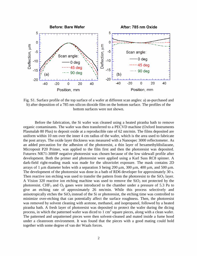
To create a nanoscale gap spacing, it is critical to maintain the surface of the sample as
flat as possible. Thus, we purchased a set of low-bow 10-cm-diameter Si wafers, about 500 m
thickness, with stringent specifications on the parallelism and flatness. We then measured the
surface profile of each wafer using a Bowoptic 208 stress measurement system. Unfortunately,
due to stresses within the Si wafer, a typical wafer can have a parabolic deflection profile with
about 10-20 m height variation between the center and the edge. If a 1 cm piece is cut from
such a wafer, the Si slab can have a deflection up to 150 nm, which is not readily suitable for use
to create a parallel nanoscale gap. This can be seen in Fig. S1(a), which shows the measured
surface profile of an as-purchased wafer. The top surface is convex at all the three scan angles:
0°, 45°, and 90°, indicating that deflections of up to 200 nm over 1 cm length of the sample
surface are possible and have to be reduced before the wafer is used. Note the cusp that appears
at the location of 40 mm is caused by the stitching of multiple sections of the profilometry scan.
Since bow arises from stresses within the wafer, it can be controlled to certain degree by
applying a tensile stress via depositing a silicon dioxide layer on one side of the wafer, though
the oxide layer generally cannot fix an irregular surface profile such as a saddle shape. Chemical
vapor deposition can be used to deposit a stress-free SiO2 film at 300°C on the heated Si wafer.
After the wafer cools to room temperature, the mismatch in the coefficients of thermal expansion
between Si and SiO2 causes the wafer to deflect, making the uncoated side less convex. There
exists a close-to-linear relationship between the thickness of the oxide and the change in the
deflection, but the coefficient in the relationship is different for different wafers. As such, each
wafer was tested with an arbitrary film thickness to estimate the correct value of oxide film
thickness. After the test, the oxide film was removed using either reactive ion etching or wet
etching in a bath of hydrofluoric acid. The profile of the bare surface was remeasured to assure
no additional stresses were introduced by the coating and removal process. Subsequently, the
correct oxide layer was deposited. Fig. S1(b) shows the effect of the oxide layer on the bow
reduction of the top side of the wafer. A 785-nm-thick layer of oxide deposited on the bottom of
the wafer changes the radius of curvature of the top surface from about 75 m to 507 m along the
0 scan line. With this procedure, the maximum deflection over the entire top wafer surface can
be limited to about 3 m and the wafer can be used to make samples. †
Equal contribution
* Corresponding author: [email protected]
2
Fig. S1. Surface profile of the top surface of a wafer at different scan angles: a) as-purchased and
b) after deposition of a 785 nm silicon dioxide film on the bottom surface. The profiles of the
bottom surfaces were not shown.
Before the fabrication, the Si wafer was cleaned using a heated piranha bath to remove
organic contaminants. The wafer was then transferred to a PECVD machine (Oxford Instruments
Plasmalab 80 Plus) to deposit oxide at a reproducible rate of 62 nm/min. The films deposited are
uniform within 10 nm over the inner 4 cm radius of the wafer, which is the area used to fabricate
the post arrays. The oxide layer thickness was measured with a Nanospec 3000 reflectometer. As
an added precaution for the adhesion of the photoresist, a thin layer of hexamethyldisilazane,
Microposit P20 Primer, was applied to the film first and then the photoresist was deposited.
Futurrex NR71-3000P negative photoresist was chosen because of the low sidewall profile after
development. Both the primer and photoresist were applied using a Karl Suss RC8 spinner. A
dark-field right-reading mask was made for the ultraviolet exposure. The mask contains 2D
arrays of 1 m diameter holes with a separation S being 200 m, 300 m, 400 m, and 500 m.
The development of the photoresist was done in a bath of RD6 developer for approximately 30 s.
Then reactive ion etching was used to transfer the pattern from the photoresist to the SiO2 layer.
A Vision 320 reactive ion etching machine was used to remove the SiO2 not protected by the
photoresist. CHF3 and O2 gases were introduced to the chamber under a pressure of 5.3 Pa to
give an etching rate of approximately 26 nm/min. While this process selectively and
anisotropically etches the SiO2 instead of the Si or photoresist, the etching time was controlled to
minimize over-etching that can potentially affect the surface roughness. Then, the photoresist
was removed by solvent cleaning with acetone, methanol, and isopropanol, followed by a heated
piranha bath. A fresh layer of photoresist was deposited to protect the wafer during the dicing
process, in which the patterned wafer was diced to 1 cm2 square pieces, along with a clean wafer.
The patterned and unpatterned pieces were then solvent-cleaned and mated inside a fume hood
under a cleanroom environment. It was found that the pieces with a good mating could hold
together with some degree of van der Waals forces.

3
Several patterned pieces not used to make samples were characterized to ensure that the
patterns created are as desired. Using a confocal microscope to test the repeatability of pattern
transfer, we found that about 98% of the pattern can be successfully transferred while less than
2% of the posts are irregularly shaped due to the photoresist posts falling over during the etching
process, likely due to poor adhesion. Figure S2 shows the Scanning Electron Microscope (SEM)
image taken with a Hitachi S4700 FESEM for a post of 800 nm height. It confirms that the
diameter is 1 m and the sidewalls can also be seen since the image was taken at a 30° angle. It
can be seen that the post is not exactly cylindrical and the top surface has some irregularities as
well as reduced area. To consider all the above-mentioned defects, the uncertainty of the cross-
sectional area for heat conduction is estimated to be 20%. The fabricated posts were also
characterized with Atomic Force Microscopy (AFM) that verifies the height of the post to be
consistent with the desired value within about 30 nm height variation.
Fig. S2. SEM image of a single post
taken at a 30° angle to show the
sidewall as well as the top surface.
Through several fabrication attempts, five wafers were successfully patterned to yield a
total of 60 samples with S = 300 m, 400 m, or 500 m. However, after mating, many samples
are not suitable for measurement as the sample either broke, presented an unacceptable gap
spacing, or had contact between the two Si pieces. A large portion of these failures is believed to
be due to small particles of dust adhering to the surface during the mating process causing
mechanical instability and a larger gap spacing. In some cases, the applied grease was too much
and the excessive grease can flow over the gap region to create a thermal pathway so that the
measured thermal resistance is essentially the contact resistances and the heat flow bypasses the
vacuum gap completely. Thus, the overall yield is about 10% if only the five wafers are counted.
This does not include the failure and numerous attempts in the earlier attempts of producing
patterns. Table S1 lists the detailed information of all the samples presented in this work,
corresponding to the 14 measurements shown in Fig. 3. They are listed in chronological order
during the near-field heat transfer measurement period from July 2015 to January 2016. For the
first three samples measured earlier, no force was applied. The rest samples use different applied
forces and are distinguished by letter a, b, c, etc. The post height is based on the film thickness
during the fabrication, while the actual spacing d is determined by FTIR measurements. For each
sample and gap spacing, multiple measurements were made with different heater powers as
shown in Fig. 2.

4
Table S1. Details of all the samples used in this work for the 14 measurements.
Wafer
No.
Sample
No.
Post
height
(nm)
S
(m)
Applied
force
(mN)
FTIR
determined
d (nm)
Uncertainty
of d (nm)
SiO2 film
thickness (nm)
patterned side
/unpatterned side
1 1 400 300 0 402 70 0/0
1 2 400 500 0 482 40 0/0
2 3 200 400 0 320 80 0/0
3 4a 200 400 0 328 80 595/785
3 4b 200 400 196 200 80 595/785
4 5a 600 500 0 762 30 0/0
4 5b 600 500 127 632 80 0/0
5 6a 800 500 0 782 40 730/785
5 6b 800 500 39 612 50 730/785
3 7a 200 400 0 512 20 595/785
3 7b 200 400 39 484 30 595/785
3 7c 200 400 78 414 60 595/785
3 7d 200 400 118 350 90 595/785
3 7e 200 400 196 336 80 595/785
S2. Dielectric function of the doped-Si wafers
As mentioned in the paper, there exists a tradeoff between the need for transparency in
the near/mid-infrared in order to determine gap spacing and opacity in the mid/far-infrared in
order to achieve significant enhancement in near-field radiative heat transfer. While the radiative
heat transfer between Si with high doping levels from 1019
to 1020
cm3
may be appealing, it
cannot be used due to the low transparency in the infrared. Through design calculations, it
appears that a 1018
cm3
doping concentration can provide sufficient transparency in the spectral
region from 2000-10000 cm1
while supporting large near-field radiative transfer mainly through
the spectral region at wavelengths longer than 5 m (or wavenumbers below 2000 cm1
).
Subsequently, we have purchased 10-cm-diameter wafers having a resistivity ranging from
0.012-0.027 Ω-cm with antimony as the n-type dopant. This resistivity range corresponds to a
doping concentration from 3×10¹⁸
to 7×10¹⁷
cm3
. A Signatone four-point probe measurement
system was used to measure the resistivity of the wafers, and the resistivity was found to be
0.016 Ω-cm averaged over four of the wafers. This gives a doping concentration of 2×10¹⁸
cm3
.
Before the samples were fabricated, we measured the transmittance (T) of all the 25 wafers using
an ABB FTLA-2000 FTIR spectrometer and, for some samples, measurements were made at

5
several different locations. The measurement indeed shows an infrared transparent window. The
excellent repeatability and agreement in the measured transmittance suggest that all wafers have
the same optical and electronic characteristics. The average thickness of the wafers is 490 m
with a variation within about ±10 m as measured with a micrometer. The spectral reflectance (R)
of several wafers was measured using a 10° reflectance accessory. The difference is negligibly
small when the wafer is flipped, indicating good uniformity and symmetry of these wafers.
Nitrogen gas was used to purge the chamber to remove carbon dioxide and water vapor
absorption in the measurement. Each measurement is an average of 64 scans with a resolution of
8 cm1
. Figure S3 displays the measured average transmittance and reflectance spectra between
500 cm1
and 10000 cm1
.
Fig. S3. Spectral reflectance and transmittance of the wafer measured by FTIR.
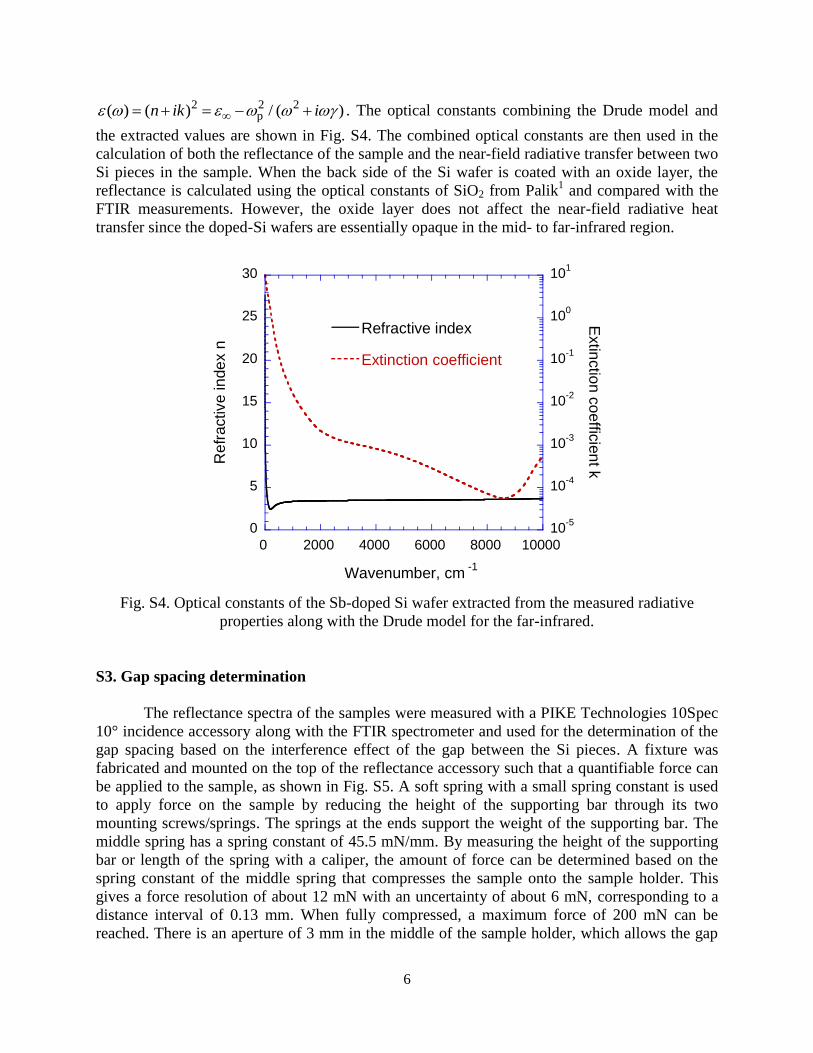
Initially, a Drude model combined with the bandgap absorption data compiled in Palik1
were used to model the dielectric function of doped silicon for calculating the reflectance and
transmittance. While the agreement is reasonable at wavenumbers below 2000 cm1
,
discrepancies occur towards large wavenumbers. The shape of the transmittance measurement
suggests that there should be some absorption near 5000 cm1
, possibly due to unknown
impurities or defects in the lattice. A wafer was annealed at 950°C for two hours at atmospheric
pressure but no change in optical properties was measured. As the optical constants in this region
are critical for predicting the vacuum gap spacing, we have developed an algorithm to extract the
refractive index n and extinction coefficient k, at discrete wavenumbers, from the measured T
and R between 1500 cm1
and 10000 cm1
.2 The extracted optical constants are very close to
Palik’s data at 9000-10000 cm1
due to bandgap absorption and close to that from the Drude
model at 1500-2000 cm1
. At lower wavenumbers, the Drude model from Basu et al.3 was used
with a plasma frequency p = 1.47×10¹⁴
rad/s, a scattering rate = 3.53×10¹³
rad/s, and a high-
frequency constant 11.7 . The dielectric function of the Drude model can be expressed as
0
0.1
0.2
0.3
0.4
0.5
0 2000 4000 6000 8000 10000
Re
flecta
nce (
R)
or
Tra
nsm
ittan
ce (
T)
Wavenumber, cm1
Sb-doped Si
R
T
6
2 2 2p( ) ( ) / ( )n ik i . The optical constants combining the Drude model and
the extracted values are shown in Fig. S4. The combined optical constants are then used in the
calculation of both the reflectance of the sample and the near-field radiative transfer between two
Si pieces in the sample. When the back side of the Si wafer is coated with an oxide layer, the
reflectance is calculated using the optical constants of SiO2 from Palik1 and compared with the
FTIR measurements. However, the oxide layer does not affect the near-field radiative heat
transfer since the doped-Si wafers are essentially opaque in the mid- to far-infrared region.
Fig. S4. Optical constants of the Sb-doped Si wafer extracted from the measured radiative
properties along with the Drude model for the far-infrared.
S3. Gap spacing determination
The reflectance spectra of the samples were measured with a PIKE Technologies 10Spec
10° incidence accessory along with the FTIR spectrometer and used for the determination of the
gap spacing based on the interference effect of the gap between the Si pieces. A fixture was
fabricated and mounted on the top of the reflectance accessory such that a quantifiable force can
be applied to the sample, as shown in Fig. S5. A soft spring with a small spring constant is used
to apply force on the sample by reducing the height of the supporting bar through its two
mounting screws/springs. The springs at the ends support the weight of the supporting bar. The
middle spring has a spring constant of 45.5 mN/mm. By measuring the height of the supporting
bar or length of the spring with a caliper, the amount of force can be determined based on the
spring constant of the middle spring that compresses the sample onto the sample holder. This
gives a force resolution of about 12 mN with an uncertainty of about 6 mN, corresponding to a
distance interval of 0.13 mm. When fully compressed, a maximum force of 200 mN can be
reached. There is an aperture of 3 mm in the middle of the sample holder, which allows the gap
0
5
10
15
20
25
30
10-5
10-4
10-3
10-2
10-1
100
101
0 2000 4000 6000 8000 10000
Refractive index
Extinction coefficient
Re
fractive in
de
x n
Extin
ctio
n c
oeffic
ien
t k
Wavenumber, cm-1

7
spacing of the sample at different locations to be measured. Gap spacings at different positions
across the sample were measured. In some cases, the gap spacing was measured at 9 points on
the sample with zero force. There were 5 measurements from one corner of the sample to the
opposite corner and then 5 more measurements along the other diagonal, with the center
measurement repeated. The change in gap spacing was not significant as compared to the gap
spacing uncertainties caused by other mentioned reasons, and should be further mitigated by
applying a force. Therefore, the uncertainty caused by the non-parallelism in the samples is
neglected. It should be noted that samples with large non-parallelism or with contact at the edges
would rule the interference patterns and these samples are excluded from further measurements.
Fig. S5. Photo of the modified reflectance
accessory, where the components are indicated
by letters as follows: a. PIKE 10Spec setup;
b. mounting bracket; c. sample holder with a
3-mm aperture, and d. supporting bar. During
the measurement, the sample or a reference is
placed under the middle spring and covers the
aperture of the sample holder. Force is applied
in a similar manner during the heat transfer
measurements.
The reflectance measurement was performed using a gold mirror as the reference. The
reflectance of the sample is determined by
sam SHAu
BG SH
I IR R
I I
(S1)
where RAu is the reflectance of gold. IBG, Isam, and ISH are the background signal measured using
the gold mirror, the signal measured using samples, and the signal measured with an open
sample holder, respectively. Measurements were typically made with 16 cm1
spectral resolution
and a large number of scans up to 512. Predicted reflectance spectra are calculated using a
multilayer matrix formulation by treating all layers as coherent. SiO2 layers are included for
samples that have oxide layers. Since the resolution of FTIR used in the measurement was much
larger than the free spectral range of the interference inside the Si wafer, spectral averaging was
applied to obtain the spectra that can be compared with experiments. In essence, the coherence
exists only in the air gap and the oxide layers, while the Si wafer is a relatively thick slab where
interference effects are negligible even though multiple reflections occur.4

8
For samples with applied forces using this fixture, position-resolved measurements were
conducted first. This measurement allows us to obtain a rough map of the deflection or non-
parallelism between the two Si pieces. Some samples can maintain a consistent gap spacing at
the center, while the edges can have contact between the Si pieces; this can be detected from the
incoherent feature of the reflectance spectrum. We tested one such sample in the heat transfer
experimental setup and the measured hrad is about 6.5 times of the calculated value. Thus, these
samples are discarded without further investigation. Only the samples that can maintain a gap
without contact at the edges were measured under different applied forces, in which case the
reflectance of the center of the sample was measured. The measurements started with 0 mN
spring force when the spring is fully extended. The supporting bar is loaded and spring length
was then reduced to the next desired force. The maximum force was limited to 200 mN
considering the yield stress of the SiO2 and Si and the results from the COMSOL simulation.2
The force was then unloaded from the maximum load to 0 mN, repeating measurements at the
same forces, to guarantee plastic deformation did not occur in the sample.
Figure S6 illustrates the agreement between the measured and calculated reflectance
spectra. For each sample, in addition to the calculated spectrum for the best-fitted gap spacing,
the calculated spectra for the upper and lower bounds of d are also shown. Six measurements are
shown here with d ranging from 200 nm to 762 nm according to Table 1, while three of them
(d = 200 nm, 402 nm, and 762 nm) are the same as those shown in Fig. 4. Note that the sample
with d = 200 nm has 595 nm of oxide film on the back of the patterned piece and 785 nm of
oxide film deposited on the back of the unpatterned piece. Similarly, the sample with d = 612 nm
has a 730 nm oxide film deposited on the back side of the patterned piece and 785 nm of oxide
film deposited on the back of the unpatterned piece.
Calculated spectra with different gap spacings are compared with the measured spectrum
to find the standard error of the estimate (SEE), which is essentially the same as the root-mean-
square deviation for all the measured wavenumber points. In calculating SEE, the spectral range
1500 cm1
to 10000 cm1
was considered for the samples with oxide, while for the samples
without oxide, 4000 cm1
to 10000 cm1
was considered since the major difference of the
reflectance spectra occurs in these ranges. The gap spacing d is determined when SEE becomes
the smallest, as illustrated in Fig. S7 for three measurements. To estimate the uncertainty in the
fitted gap spacing, we let the SEE value increase by 0.005, such that the upper and lower value
of the gap distance can be found. The uncertainty of the gap spacing is calculated as half of the
difference between the upper and lower values. The determined gap spacings and the associated
uncertainties are shown in Table S1. The uncertainty value for each sample is used as the upper
and lower limits of d in plotting the reflectance spectra shown in Fig. S6.
In some cases, the SEE reaches a local minimum at more than one gap spacing and the
most reasonable one is chosen as the fitted d. For example, for the d = 512 nm sample, another
local minimum is found at d = 114 nm but the SEE value is obviously much higher. The situation
for d = 200 nm sample is somewhat different, as can be seen in Fig. S7, the SEE value is lower at
the local minimum of d = 426 nm than at d = 200 nm. In this case, since the d value without
spring force is already 328 nm (see Table S1), upon applied force, it is logical to take d = 200 nm
as the fitted value. It should be noted that, for certain samples, the reflectance spectra are almost
indistinguishable for a relatively large range of d values. For the sample shown in the diamond

9
symbol in Fig. 3, the SEE values change little for 260 nm < d < 340 nm, as shown in Fig. S7.
Even though d = 336 nm gives the minimum SEE, reducing d to 290 nm only increases SEE by
0.001. If a value of d = 290 nm was used, the experimentally determined hrad would be reduced
due to the increased conduction contribution but the numerically calculated hrad would increase
due to the reduced gap spacing, resulting in a good agreement within the uncertainties.
Fig. S6. Determination of the gap spacing using the reflectance spectra. The spectrum of
the determined gap spacing is compared with the measurement together with the spectrum after
the uncertainty of the gap spacing is considered.

10
Fig. S7. The standard error of estimate (SEE) between the calculated and measured
reflectance as a function of d in the calculation for three measurements.
S4. Calculation of near-field thermal radiation
The origin of the strong near-field heat transfer can be explained by the spectral radiative
heat flux, q , between two semi-infinite doped-Si media, which is obtained from fluctuational
electrodynamics using dyadic Green’s functions:4,5
H L2 0
1, , ,
4q T T d
(S2)
Here, B( ) exp, 1k TT is the average energy of a Planck oscillator, where is
the reduced Planck constant, is the angular frequency and kB is the Boltzmann constant. In Eq.
(S2), represents the magnitude of the wave vector parallel to the heat transfer interface, and
( , ) is the photon tunneling probability (also called energy transmission coefficient) that
includes both polarizations. Equation (S2) is integrated to obtain the total radiative heat transfer
rate or heat transfer coefficient as shown in Figs. 2 and 3. The predicted spectral heat flux is
shown in Fig. S8 with various gap spacings, when the emitter and receiver temperatures are set
to 320 K and 300 K, respectively. Two peaks can be identified on the plot especially at small gap
spacings. The sharp peak at the lower frequency is caused by the high density of states of
coupled surface plasmon polaritons (for transverse magnetic waves only) when the real part of
the dielectric function of doped-Si is around 1, and the other broader peak is due to the
frequency dependence of the Planck oscillator.4 Since the field intensity of surface plasmons
exponentially decay away from the interface, a smaller gap distance promotes the coupling of
surface plasmons at the vacuum-Si interfaces, mediating more efficient photon tunneling at large
and resulting in higher spectral heat flux.5
0
0.02
0.04
0.06
0.08
0.1
200 400 600 800
d = 200 nm
d = 336 nm
d = 512 nm
SE
E
Gap spacing d, nm

11
0
10
20
30
40
0 1 2 3 4 5
d = 100 nm
d = 200 nm
d = 500 nm
d = 1 m
q''
, pJ/m
2-r
ad
Angular frequency 1014
rad/s
TH = 320 K
TL = 300 K
Fig. S8. Calculated spectral radiative heat flux at different gap spacings based on
fluctuational electrodynamics. The emitter and receiver temperatures are 320 and 300 K,
respectively.
S5. Uncertainty analysis
The uncertainty in d is relatively large and it affects the calculated results and the
determination of the contribution of heat conduction. In the measurements, the samples were
mounted on the stack and a spring (same as the one in the force-controlled FTIR reflectance
measurements) was used on top of the heater. The length of the spring was measured and the
amount of force applied to the sample can be calculated. The uncertainty of d is determined for
each sample based on the FTIR measurements displayed in Table S1. Additionally, since the
applied force has uncertainty (about 6 mN) and the weight of the components above the sample
(about 20 mN) can also bring uncertainty to the applied force, an uncertainty of 20 nm in gap
spacing is considered to be combined with the uncertainty determined from the FTIR
measurements.
The LakeShore DT-670 silicon diode thermistor is calibrated by the manufacturer and
tested to be accurate within 37 mK in the temperature range used here. The uncertainty of the
temperature comes from the thermoelectric circuit. It is made of two Omega 40AWG E-type
thermocouples by bonding the constantan wires together using a thermocouple welder, such that
the output voltage can be directly used to obtain the temperature difference between the two
normal chromel-constantan junctions. The uncertainty of the thermoelectric circuit is 0.15°C
determined by calibration using an Engineering Model 12001-A-12-6-2-A/LT14 resistance
thermal detector.2

12
The measured radiative heat transfer rate is obtained by excluding the conduction
contribution from the measured heat rate, i.e., rad HFM condq q q . Thus, the uncertainty of the
measured radq depends on the total heat rate measurement and the conduction estimation. The
uncertainty of qrad as well as hrad can be determined based on an error propagation analysis. The
uncertainty of the heat flux meter is estimated to be 4.4% as determined from a calibration
experiment using PTFE samples whose thermal conductivity were determined by measuring the
specific heat and the thermal diffusivity using a differential scanning calorimeter and a light flash
technique, correspondingly.2 The resulting value for the sensitivity is 6.87 V-cm
2/mW, as
compared with 7.88 V-cm2/mW provided by the manufacturer since the manufacturer’s
calibration was not done with the same setup.
The heat conduction rate is calculated using a simple one-dimensional conduction model
by assuming all the posts have the same height d . Since the thermal resistance associated with
crossing the vacuum gap is so much larger than the lateral resistance in the silicon plates, the
temperature is assumed to be uniform with each Si piece. Hence, the heat transfer rate by
conduction is found as
post
cond post
Aq N T
d
(S3)
where postA is cross-sectional area of each post and the number of posts is 2 2post 1 cm /N S .
The value of thermal conductivity of SiO2 is taken as 1.4±0.1 W/m-K, considering the possible
effects of phonon-boundary scattering. The number of posts is assumed to have no uncertainties,
while in contrast the uncertainty is considered as 20% in the cross-sectional area of the post.
It should be noted that using such a model to calculate the conduction is not ideal;
however, fully quantifying the conduction is very challenging using current techniques. This
would require complete knowledge of the height distribution and contact area of the posts, the
thermal contact resistance between the SiO2 posts and the Si wafer, the exact surface profiles of
both pieces, and the way that the sample deforms when external forces are applied, etc. Many of
these factors are expected to vary between samples and in situ measurements would be required
for unambiguous determinations. Considering this, the above-mentioned model was used to
calculate the conduction contribution with a rather large estimated uncertainty to compensate for
the difficulties in accurate determination of heat conduction. This can be a major limitation of
current experiment design and may be improved in future works.
It is important to limit the conduction heat transfer in many practical applications
utilizing near-field thermal radiation. Reducing the conduction heat transfer can also improve the
near-field radiation measurement accuracy. Figure S9 shows the contribution of radiation to the
total heat transfer. It can be seen that the radiation contribution is above 65%, except for Sample
1 (S = 300 m and d = 402 nm) for which conduction contributes 44% to the heat transfer.
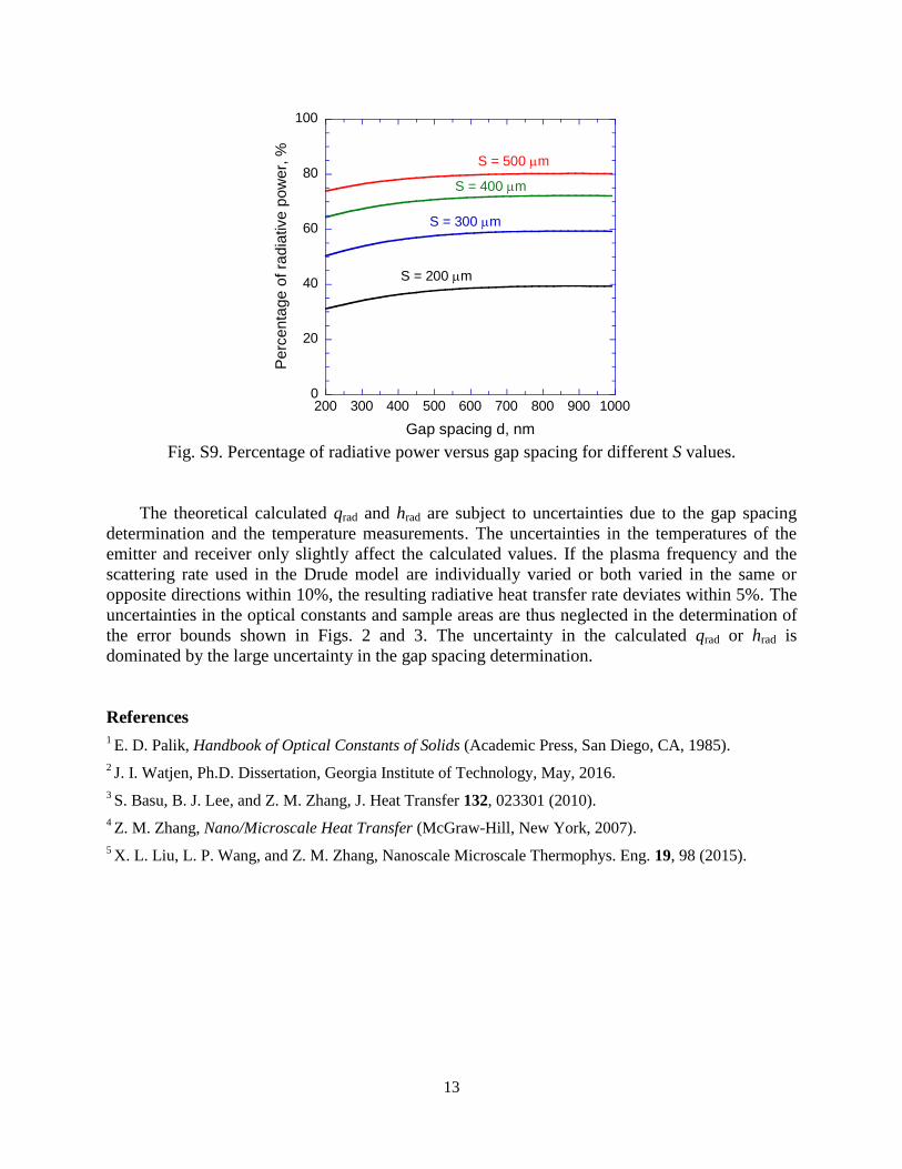
13
Fig. S9. Percentage of radiative power versus gap spacing for different S values.
The theoretical calculated qrad and hrad are subject to uncertainties due to the gap spacing
determination and the temperature measurements. The uncertainties in the temperatures of the
emitter and receiver only slightly affect the calculated values. If the plasma frequency and the
scattering rate used in the Drude model are individually varied or both varied in the same or
opposite directions within 10%, the resulting radiative heat transfer rate deviates within 5%. The
uncertainties in the optical constants and sample areas are thus neglected in the determination of
the error bounds shown in Figs. 2 and 3. The uncertainty in the calculated qrad or hrad is
dominated by the large uncertainty in the gap spacing determination.
References
1 E. D. Palik, Handbook of Optical Constants of Solids (Academic Press, San Diego, CA, 1985).
2 J. I. Watjen, Ph.D. Dissertation, Georgia Institute of Technology, May, 2016.
3 S. Basu, B. J. Lee, and Z. M. Zhang, J. Heat Transfer 132, 023301 (2010).
4 Z. M. Zhang, Nano/Microscale Heat Transfer (McGraw-Hill, New York, 2007).
5 X. L. Liu, L. P. Wang, and Z. M. Zhang, Nanoscale Microscale Thermophys. Eng. 19, 98 (2015).
0
20
40
60
80
100
200 300 400 500 600 700 800 900 1000
Pe
rce
nta
ge
of ra
dia
tive
po
we
r, %
Gap spacing d, nm
S = 200 m
S = 300 m
S = 400 m
S = 500 m