near-field observation of anomalous optical propagation in photonic crystal coupled-cavity...
TRANSCRIPT
Near-field observation of anomalous optical
propagation in photonic crystal coupled-cavity
waveguides
Haihua Tao,1, 2
Cheng Ren,2 Yazhao Liu,
2 Qingkang Wang,
1 Daozhong Zhang,
2 and
Zhiyuan Li2,*
1RIMNST, Shanghai Jiao Tong University, Shanghai 200240, China
2Laboratory of Optical Physics, Institute of Physics, Chinese Academy of Sciences, Beijing 100190, China
Abstract: An air-bridged silicon-based photonic crystal coupled-cavity
waveguide (PCCCW) connected with an input and output W1 PC waveguide
(PCW) was designed and fabricated. We mapped its intensity distributions
with a near-field scanning optical microscope (NSOM) at near-infrared
wavelengths around 1550 nm. Surprisingly, the intensity distributions
demonstrate that the second odd eigenmode dominates in such a PCCCW,
even though it possesses a much slower group velocity of light than that of the
first even one. Further considering the measured transmission spectrum, we
find that the modal profile and impedance matching between the eigenmodes
in the PCW and PCCCW plays an important role in the optical propagation
efficiency. Mode conversion between the first even and the second odd
eigenmode was also detected at the interfaces between the W1 PCW and
PCCCW.
©2010 Optical Society of America
OCIS codes: (130.5296) Photonic crystal waveguides; (180.4243) Near-field microscopy;
(230.4555) Coupled resonators; (999.9999) Slow light.
References and links
1. T. Baba, “Slow light in photonic crystals,” Nat. Photonics 2(8), 465–473 (2008).
2. S. Mookherjea, J. S. Park, S. Yang, and P. R. Bandaru, “Localization in silicon nanophotonic slow-light
waveguides,” Nat. Photonics 2(2), 90–93 (2008).
3. M. S. Moreolo, V. Morra, and G. Cincotti, “Design of photonic crystal delay lines based on enhanced
coupled-cavity waveguides,” J. Opt. A, Pure Appl. Opt. 10(6), 064002 (2008).
4. J. Hou, H. Wu, D. S. Citrin, W. Mo, D. Gao, and Z. Zhou, “Wideband slow light in chirped slot photonic-crystal
coupled waveguides,” Opt. Express 18(10), 10567–10580 (2010).
5. T. Baba, T. Kawaaski, H. Sasaki, J. Adachi, and D. Mori, “Large delay-bandwidth product and tuning of slow light
pulse in photonic crystal coupled waveguide,” Opt. Express 16(12), 9245–9253 (2008).
6. B. Corcoran, C. Monat, C. Grillet, D. J. Moss, B. J. Eggleton, T. P. White, L. O’Faolain, and T. F. Krauss, “Green
light emission in silicon through slow-light enhanced third-harmonic generation in photonic-crystal waveguides,”
Nat. Photonics 3(4), 206–210 (2009).
7. L. H. Frandsen, A. V. Lavrinenko, J. Fage-Pedersen, and P. I. Borel, “Photonic crystal waveguides with semi-slow
light and tailored dispersion properties,” Opt. Express 14(20), 9444–9450 (2006).
8. V. S. Volkov, S. I. Bozhevolnyi, L. H. Frandsen, and M. Kristensen, “Direct observation of surface mode excitation
and slow light coupling in photonic crystal waveguides,” Nano Lett. 7(8), 2341–2345 (2007).
9. V. S. Volkov, S. I. Bozhevolnyi, P. I. Borel, L. H. Frandsen, and M. Kristensen, “Near-field characterization of
low-loss photonic crystal waveguides,” Phys. Rev. B 72(3), 035118–035124 (2005).
10. A. Yariv, Y. Xu, R. K. Lee, and A. Scherer, “Coupled-resonator optical waveguide: a proposal and analysis,” Opt.
Lett. 24(11), 711–713 (1999).
11. A. Martínez, A. García, P. Sanchis, and J. Martí, “Group velocity and dispersion model of coupled-cavity
waveguides in photonic crystals,” J. Opt. Soc. Am. A 20(1), 147–150 (2003).
12. T. J. Karle, D. H. Brown, R. Wilson, M. Steer, and T. F. Krauss, “Planar photonic crystal coupled cavity
waveguides,” IEEE J. Sel. Top. Quantum Electron. 8(4), 909–918 (2002).
13. A. Talneau, G. Aubin, A. Uddhammar, A. Berrier, M. Mulot, and S. Anand, “Highly dispersive photonic
crystal-based coupled-cavity structures,” Appl. Phys. Lett. 88(20), 201106 (2006).
#133202 - $15.00 USD Received 10 Aug 2010; revised 25 Oct 2010; accepted 26 Oct 2010; published 2 Nov 2010(C) 2010 OSA 8 November 2010 / Vol. 18, No. 23 / OPTICS EXPRESS 23994

14. M. L. Povinelli, and S. H. Fan, “Radiation loss of coupled-resonator waveguides in photonic-crystal slabs,” Appl.
Phys. Lett. 89(19), 191114 (2006).
15. C. J. Jin, N. P. Johnson, H. M. H. Chong, A. S. Jugessur, S. Day, D. Gallagher, and R. M. De La Rue,
“Transmission of photonic crystal coupled-resonator waveguide (PhCCRW) structure enhanced via mode
matching,” Opt. Express 13(7), 2295–2302 (2005).
16. P. Sanchis, J. Marti, P. Bienstman, and R. Baets, “Semianalytic approach for analyzing coupling issues in photonic
crystal structures,” Appl. Phys. Lett. 87(20), 203107 (2005).
17. P. Sanchis, J. Martí, W. Bogaerts, P. Dumon, D. Van Thourhout, and R. Baets, “Experimental results on adiabatic
coupling into SOI photonic crystal coupled-cavity waveguides,” IEEE Photon. Technol. Lett. 17(6), 1199–1201
(2005).
18. Y. A. Vlasov, and S. J. McNab, “Coupling into the slow light mode in slab-type photonic crystal waveguides,” Opt.
Lett. 31(1), 50–52 (2006).
19. M. Notomi, K. Yamada, A. Shinya, J. Takahashi, C. Takahashi, and I. Yokohama, “Extremely large group-velocity
dispersion of line-defect waveguides in photonic crystal slabs,” Phys. Rev. Lett. 87(25), 253902 (2001).
20. Z. Y. Li, L. L. Lin, and K. M. Ho, “Light coupling with multimode photonic crystal waveguides,” Appl. Phys. Lett.
84(23), 4699–4701 (2004).
21. H. Gersen, T. J. Karle, R. J. P. Engelen, W. Bogaerts, J. P. Korterik, N. F. van Hulst, T. F. Krauss, and L. Kuipers,
“Real-space observation of ultraslow light in photonic crystal waveguides,” Phys. Rev. Lett. 94(7),
073903–073905 (2005).
22. B. Cluzel, D. Gérard, E. Picard, T. Charvolin, V. Calvo, E. Hadji, and F. de Fornel, “Experimental demonstration of
Bloch mode parity change in photonic crystal waveguide,” Appl. Phys. Lett. 85(14), 2682–2684 (2004).
23. P. Tortora, M. Abashin, I. Märki, W. Nakagawa, L. Vaccaro, M. Salt, H. P. Herzig, U. Levy, and Y. Fainman,
“Observation of amplitude and phase in ridge and photonic crystal waveguides operating at 1.55 microm by use of
heterodyne scanning near-field optical microscopy,” Opt. Lett. 30(21), 2885–2887 (2005).
24. M. Abashin, P. Tortora, I. Märki, U. Levy, W. Nakagawa, L. Vaccaro, H. P. Herzig, and Y. Fainman, “Near-field
characterization of propagating optical modes in photonic crystal waveguides,” Opt. Express 14(4), 1643–1657
(2006).
25. N. Louvion, D. Gérard, J. Mouette, F. de Fornel, C. Seassal, X. Letartre, A. Rahmani, and S. Callard, “Local
observation and spectroscopy of optical modes in an active photonic-crystal microcavity,” Phys. Rev. Lett. 94(11),
113907 (2005).
26. B. Cluzel, E. Picard, T. Charvolin, E. Hadji, L. Lalouät, F. de Fornel, C. Sauvan, and P. Lalanne, “Near-field
spectroscopy of low-loss waveguide integrated microcavities,” Appl. Phys. Lett. 88(5), 051112–051114 (2006).
27. S. I. Bozhevolnyi, V. S. Volkov, T. Søndergaard, A. Boltasseva, P. I. Borel, and M. Kristensen, “Near-field
imaging of light propagation in photonic crystal waveguides: Explicit role of Bloch harmonics,” Phys. Rev. B
66(23), 235204 (2002).
28. H. H. Tao, R. J. Liu, Z. Y. Li, S. Feng, Y. Z. Liu, C. Ren, B. Y. Cheng, D. Z. Zhang, H. Q. Ma, L. A. Wu, and Z. B.
Zhang, “Mapping of complex optical field patterns in multimode photonic crystal waveguides by near-field
scanning optical microscopy,” Phys. Rev. B 74(20), 205111 (2006).
29. A. Mekis, S. H. Fan, and J. D. Joannopoulos, “Absorbing boundary conditions for FDTD simulations of photonic
crystal waveguides,” IEEE Microw. Guid. Wave Lett. 9(12), 502–504 (1999).
30. A. Farjadpour, D. Roundy, A. Rodriguez, M. Ibanescu, P. Bermel, J. D. Joannopoulos, S. G. Johnson, and G. W.
Burr, “Improving accuracy by subpixel smoothing in FDTD,” Opt. Lett. 31, 2972–2974 (2006).
1. Introduction
Slow light has attracted significant interest recently as a potential solution for optical delay line,
time-domain optical signal processing, and amplifiers of nonlinear optical effects in the
integrated photonic circuits [1–6]. For realizing slow light, two-dimensional silicon photonic
crystal waveguides (PCWs) have proven to be a powerful platform, as it is compatible with
on-chip integration and can offer wide bandwidth [5,6]. One way for this purpose is to utilize
the flat edges of photonic band dispersion curves, which consequently result in slow group
velocity [7–9]. The other one is to design photonic crystal coupled-cavity waveguides
(PCCCWs), in which the eigenmodes usually have relatively narrow bandwidth with slow
group velocity in the whole band range. For PCCCWs, the optical propagation is different from
the conventional PCWs, in which light propagates by hopping from one cavity to another in the
form of local resonant modes [5,10–17]. In all waveguides, transmission efficiency is an
important issue for its applications. Usually, slow light could intrinsically result in rather low
transmission efficiency due to increasing light-matter interaction as well as the extrinsic
influence from index and group velocity mismatches at interfaces [1,2,14–20]. As is well
known, near-field scanning optical microscopy (NSOM) provides an efficient tool to uncover
the essence of light propagation by mapping the optical field distributions with a subwavelength
#133202 - $15.00 USD Received 10 Aug 2010; revised 25 Oct 2010; accepted 26 Oct 2010; published 2 Nov 2010(C) 2010 OSA 8 November 2010 / Vol. 18, No. 23 / OPTICS EXPRESS 23995
resolution in nanophotonics [8,9,21–28]. Till now, slow light propagation in such specific
PCCCWs is still not experimentally studied via NSOM technique. In this article, we design a
silicon-based air-bridged PCCCW structure with slow light and study its optical propagation at
near-infrared wavelengths. The measured transmission spectrum, near-field optical mapping of
intensity distributions, and theoretical simulation results all demonstrate that the second odd
eigenmode of the PCCCW has significantly higher transmission efficiency than that of the first
even one, even though it possesses a lower group velocity. This anomalous optical propagation
has not been reported in previous literatures. Mode conversion between the first even and the
second odd eigenmode is also found at the interfaces between the W1 PCWs and PCCCW.
2. Theoretical design
PCCCW structures based on a conventional W1 PCW (a triangular lattice photonic crystal
membrane with a line of air holes unetched along the ΓΚ direction) with alternate identical air
holes have attracted specific attention and been studied especially for improving the optical
coupling efficiency from external medium [12,15–17]. However, to our knowledge, this kind of
PCCCW with decreased alternate air holes, which can improve the transmission efficiency, has
not been reported. In this study, we design such kind of silicon-based air-bridged PCCCW
structure working at around 1580 nm by means of the three-dimensional (3D) finite-difference
time-domain (FDTD) method [29,30]. As for the silicon-on-insulator (SOI) substrate, the
thickness of the silicon film is 235 nm with the refractive index to be 3.5. The refractive index of
the air background is taken to be 1. The lattice constant and the radius of the air holes in the
background triangular lattice photonic crystal are designed to be α = 455 nm and R0 = 126 nm,
respectively. For such a design, the W1 PCW could transmit TE-polarized light in the region
from 1500 to 1640 nm. The radius of the alternate small holes (radius) along the central
waveguide axis is Rd = 112 nm, forming a guided band centered at around 1580 nm for the
PCCCW.
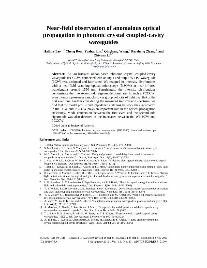
Figure 1 plots band diagrams of the PCCCW (with an inset of the supercell for calculation)
and the traditional W1 PCW for TE-polarized modes with parameters as designed above. The
W1 PCW model structure is coherent with the discussion in the rest of the article, in which it
works as the input and output waveguides of the actual structure and helps to increase the
coupling efficiency between the ridge waveguides and the PCCCW [15–17]. For both
structures, there exist two low-order eigenmodes, i.e., the first even mode and the second odd
mode, which are denoted by the triangular and circular dotted lines, respectively. Here the even
and odd eigenmodes have the mirror-reflection symmetry with respect to the plane passing
through the central axis of the waveguide and perpendicular to the slab. Comparing the
calculated band diagrams of the PCCCW and W1 PCW, we can clearly see that both resonant
eigenmodes of the PCCCW in the whole frequency region is completely covered by the
corresponding guided mode band in the W1 PCW. On the other hand, at a certain frequency the
W1 PCW supports eigemodes while they are absent in the PCCCW. In addition, the bandwidth
of the odd eigenmode is totally covered by that of the even mode in both the W1 PCW and
PCCCW.
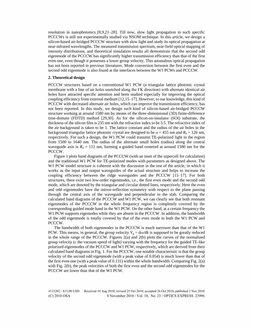
The bandwidth of both eigenmodes in the PCCCW is much narrower than that of the W1
PCW. This means, in general, the group velocity Vg = dω/dk is supposed to be greatly reduced
in the whole range of the PCCCW. Figures 2(a) and 2(b) plots the curves of the normalized
group velocity (c the vacuum speed of light) varying with the frequency for the guided TE-like
polarized eigenmodes of the PCCCW and W1 PCW, respectively, which are derived from their
calculated band diagrams in Fig. 1. For the PCCCW, one notable characteristic is that the group
velocity of the second odd eigenmode (with a peak value of 0.054) is much lower than that of
the first even one (with a peak value of 0.131) within the whole bandwidth. Comparing Fig. 2(a)
with Fig. 2(b), the peak velocities of both the first even and the second odd eigenmodes for the
PCCCW are lower than that of the W1 PCW.
#133202 - $15.00 USD Received 10 Aug 2010; revised 25 Oct 2010; accepted 26 Oct 2010; published 2 Nov 2010(C) 2010 OSA 8 November 2010 / Vol. 18, No. 23 / OPTICS EXPRESS 23996
0.0 0.1 0.2 0.3 0.4 0.50.26
0.27
0.28
0.29
0.30
0.31
0.32
1750
1700
1650
1600
1550
1500
1450
Fre
qu
en
cy
(
/)
Wavevector (2/)
Odd Mode
Even Mode
light cone
(:n
m)
(b)
0.00 0.05 0.10 0.15 0.20 0.25
0.270
0.275
0.280
0.285
0.290
0.295
0.300
0.305
0.310
1680
1650
1620
1590
1560
1530
1500
1470
Even mode
Odd mode
Wavevector (2) (:n
m)
Fre
qu
en
cy
(
/)
(a)
Fig. 1. Calculated band diagrams of (a) the PCCCW with an inset of the supercell model (Rd =
112 nm) and (b) the traditional W1 PCW for the TE-like polarized modes.
0.270 0.285 0.300 0.315 0.330
0.00
0.05
0.10
0.15
0.20
0.25
high K
low K
W1 even mode
W1 odd modeV
g(c
)
Frequency (/)
(b)
0.280 0.285 0.290 0.2950.00
0.02
0.04
0.06
0.08
0.10
0.12
0.14
Vg(c
)
Frequency (/)
CCW even mode
CCW odd mode (a)
Fig. 2. (a) Normalized group velocity as a function of frequency for TE-like polarized
eigenmodes of PCCCW and (b) that of the traditional W1 PCW derived from Fig. 1.
3. Fabrication and experimental results
We fabricated the PCCCW on the silicon-on-insulator wafers with a focused ion beam machine
followed by the chemical etching in hydrofluoric acid to form an air-bridged silicon membrane
2D PC structure. The transmission spectrum was detected by a far-field optical detection system
equipped with a continuous wave (cw) wavelength-tunable laser from 1500 to 1640 nm with the
power fixed at 3 mW. An infrared CCD camera (HAMAMATSU MODEL C2741-03), which
was connected with an objective (M Plan Apo NIR, 100X/0.5N.A.), could take a picture with
the field of view 127 × 95 µm2. The near-field intensity distribution profiles were mapped using
an NSOM system (NSOM-100 Nanonics, Israel) in collection mode with the same cw laser
source. The output signal was probed by an inhouse developed InGaAs single-photon detector.
The NSOM tip, a cantilever metal-coated fiber with an aperture diameter of 200 nm, was
controlled to scan at a constant-height position of ~10 nm above the sample surface. More
details of the fabrication and optical detection techniques can be found in Ref. 28.
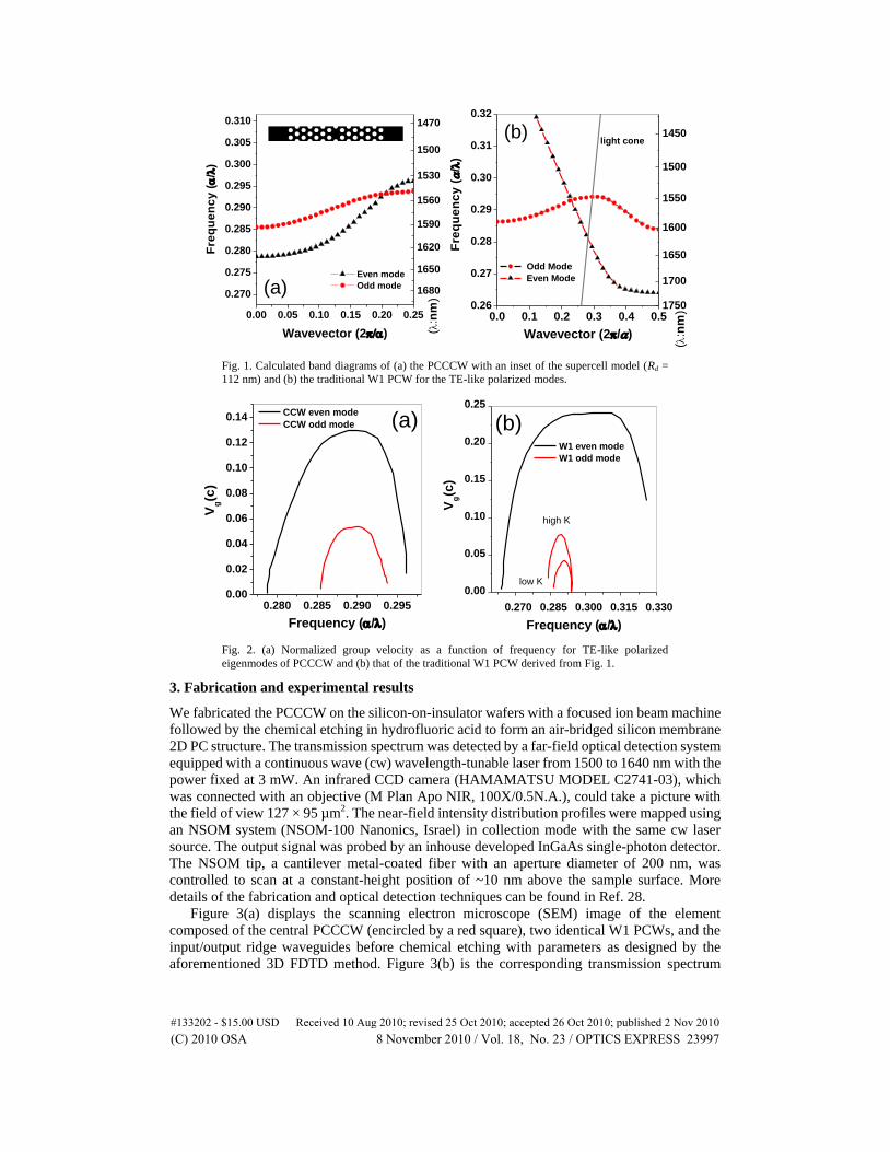
Figure 3(a) displays the scanning electron microscope (SEM) image of the element
composed of the central PCCCW (encircled by a red square), two identical W1 PCWs, and the
input/output ridge waveguides before chemical etching with parameters as designed by the
aforementioned 3D FDTD method. Figure 3(b) is the corresponding transmission spectrum
#133202 - $15.00 USD Received 10 Aug 2010; revised 25 Oct 2010; accepted 26 Oct 2010; published 2 Nov 2010(C) 2010 OSA 8 November 2010 / Vol. 18, No. 23 / OPTICS EXPRESS 23997

with a guided band ranging from 1555 to 1614 nm as measured by the far-field optical detection
system. This narrow guided bandwidth is consistent with the calculated band curves in Fig. 1(a).
At outlet of the element, a bright spot is detectable in the region of guided band, as depicted by
a partial CCD image at 1580 nm in the inset of Fig. 3(b).
1500 1530 1560 1590 1620-70
-65
-60
-55
-50
-45
-40
-35
Tra
ns
mis
sio
n (
dB
m)
Wavelength (nm)
(b)
(a)
Fig. 3. (a) SEM image of the element composed of the central PCCCW, two identical W1 PCWs
and the input/output ridge waveguides; (b) Measured transmission spectrum with the inset of a
bright optical spot image at 1580 nm at the outlet observed by the infrared CCD camera.
Figure 4 displays the near-field optical intensity distribution patterns of the PCCCW at
different wavelengths within the guided bandwidth. The scanning area is 12 × 15 μm2 with the
incident light propagating upwards from the bottom of the image. The straight yellow lines in
Figs. 4(b)-4(d), and 4(f) are used to label the position for showing the cross-sectional profiles of
the field distribution patterns. The results are displayed in Fig. 5. For clarity, the SEM picture of
the PCCCW is inserted in Fig. 4(a) instead of the NSOM topography with the same scanning
area as the latter has a much coarser topographical resolution.
We first focus on the near-field optical images at 1550 and 1610 nm [Figs. 4(b) and 4(f)]
which appear dissipating pretty quickly along the PCCCW section with relatively low
transmission efficiency as indicated in the transmission spectrum of Fig. 3(b). The optical
intensity distribution patterns are different at 1550 and 1610 nm, even though both of them
mainly appear as a single narrow line along the central PCCCW region with a full width at half
maximum (FWHM) of ~350 nm. Precisely speaking, the pattern demonstrates a little bit
shoulder as a result of mode superposition at 1550 nm, since it comprises two eigenmodes. At
1610 nm, the pattern appears bright and wide with obvious interference nodes in the PCCCW
section.
#133202 - $15.00 USD Received 10 Aug 2010; revised 25 Oct 2010; accepted 26 Oct 2010; published 2 Nov 2010(C) 2010 OSA 8 November 2010 / Vol. 18, No. 23 / OPTICS EXPRESS 23998
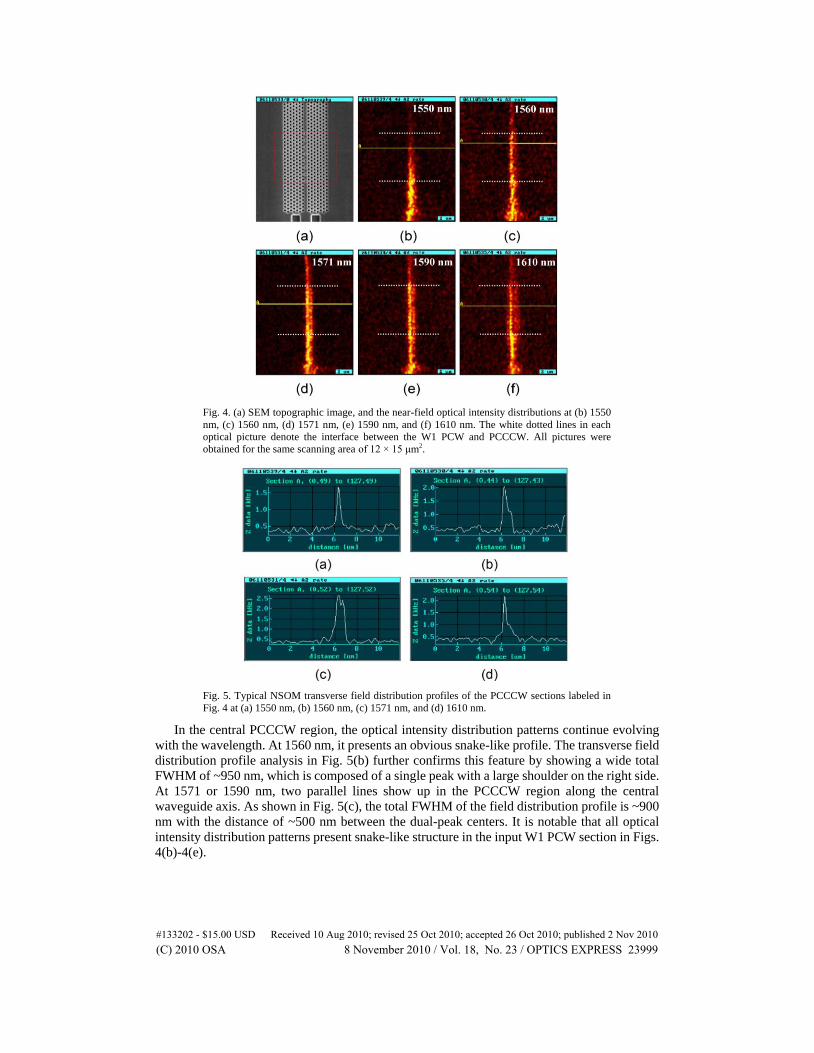
Fig. 4. (a) SEM topographic image, and the near-field optical intensity distributions at (b) 1550
nm, (c) 1560 nm, (d) 1571 nm, (e) 1590 nm, and (f) 1610 nm. The white dotted lines in each
optical picture denote the interface between the W1 PCW and PCCCW. All pictures were
obtained for the same scanning area of 12 × 15 μm2.
Fig. 5. Typical NSOM transverse field distribution profiles of the PCCCW sections labeled in
Fig. 4 at (a) 1550 nm, (b) 1560 nm, (c) 1571 nm, and (d) 1610 nm.
In the central PCCCW region, the optical intensity distribution patterns continue evolving
with the wavelength. At 1560 nm, it presents an obvious snake-like profile. The transverse field
distribution profile analysis in Fig. 5(b) further confirms this feature by showing a wide total
FWHM of ~950 nm, which is composed of a single peak with a large shoulder on the right side.
At 1571 or 1590 nm, two parallel lines show up in the PCCCW region along the central
waveguide axis. As shown in Fig. 5(c), the total FWHM of the field distribution profile is ~900
nm with the distance of ~500 nm between the dual-peak centers. It is notable that all optical
intensity distribution patterns present snake-like structure in the input W1 PCW section in Figs.
4(b)-4(e).
#133202 - $15.00 USD Received 10 Aug 2010; revised 25 Oct 2010; accepted 26 Oct 2010; published 2 Nov 2010(C) 2010 OSA 8 November 2010 / Vol. 18, No. 23 / OPTICS EXPRESS 23999

4. Analysis and discussion
With the calculated band diagrams of the PCCCW and W1 PCW in Fig. 1 at hand, we now
move forward to get the field distributions at different wavelengths by means of the 3D FDTD
method. The light source has a Gaussian profile with even or odd symmetry relative to the
waveguide axis. Figures 6(a1)-6(e1) show the calculated optical field distribution profiles at
different wavelengths with a simulation model schematized in Fig. 6(M1). When it contains
only the first even eigenmode, an even symmetric source is used [at 1610 nm in Fig. 6(e1)]. In
this case, only the first even eigenmode can be excited. The calculated result consists well with
the experimental one in Fig. 4(f) presenting a single line along the whole waveguide. When the
first even and the second odd eigenmodes coexist, a superposed continuous wave source with
equal even and odd eigenmode amplitudes is used [Figs. 6(a1)-6(d1)]. In this case, both the first
even and the second odd eigenmodes can be excited. The simulated field distribution profiles in
the W1 PCW sections agree well with the detected ones at all these wavelengths, which show a
snake-like/single-line profile in the input/output W1 PCW except that of a snake-like profile in
the output W1 PCW at 1560 nm. In addition, the simulated field distribution patterns of the
snake-like profile in the PCCCW section appear deviating greatly from the detected ones at
1550, 1571, and 1590 nm. In order to explain such discrepancies, we use a model of the
PCCCW in Fig. 6(M2) for further theoretical simulation. The optical field distribution patterns
at 1550, 1560, and 1571 nm are displayed in Figs. 6(a2)-6(c3) with the even-to-odd amplitude
ratios of 1:4, 1:1, 1:4, and 1:6, respectively. The calculated field distributions at 1590 nm, which
are similar to those at 1571 nm with the same trend as the experimental results in Fig. 4, are not
otherwise displayed for concision. With this model, the simulated results are consistent with the
experimental patterns evolving from single, to snake-like, and then to double-line structures for
the PCCCW section. Calculation of the field distribution displayed in Fig. 6(a2) further shows
that the first even eigenmode still dominates in the PCCCW even if the even-to-odd amplitude
ratio is only 1:4. This means that the component of the odd eigenmode increases when the
wavelength grows from 1550 to 1571 nm.
As pointed out in Fig. 2(a), in general, the group velocity of the second odd eigenmode is
much slower than that of the first even one. According to previous studies, a slow group
velocity means long transit time per distance, and this can result in large dissipation due to
material absorption and radiation losses [14,15,17]. Furthermore, a slow group velocity means
low coupling efficiency at the interfaces due to large impedance mismatch [18,19]. However, in
our current study, the second odd eigenmode dominates with a result of high total transmission
efficiency in the central frequency region. This means that the group velocity of different modes
is not a critical factor in determining the transmission efficiency of the PCCCW. The reason
might be that the PCCCW has a distance comprising only seven cavities, and therefore the
group velocity induced loss is not a dominant factor.
Another factor, i.e. the modal profile and impedance matching between the eigenmodes in
the W1 PCW and PCCCW, seems to play a more important role in the transmission efficiency
of the PCCCW. In the PCCCW, the waveguide along the alternate small air hole axis has a
relatively low effective refractive index. For the second odd eigenmode, its energy distributes
mainly away from the central axis, therefore the modal profile mismatch between the PCW odd
mode and the PCCCW odd mode could be relatively small. In contrast, for the first even mode,
its energy mainly concentrates on the central line, light sees very different environment in the
PCW and PCCCW and the modal impedance is strong. Light could thus suffer more serious
interface reflection and radiation losses when it propagates across the interfaces between the
W1 PCW and PCCCW. As a result, the transmission efficiency gets relatively lower for the first
even eigenmode, even though its group velocity is higher than that of the second odd mode. For
the second odd eigenmode at around 1550 nm, the low propagation efficiency could be related
to the spreading structure of the second odd mode due to its extremely slow group velocity near
the cutoff of the PCCCW. When the incident wavelength gets larger, the mode group velocity
#133202 - $15.00 USD Received 10 Aug 2010; revised 25 Oct 2010; accepted 26 Oct 2010; published 2 Nov 2010(C) 2010 OSA 8 November 2010 / Vol. 18, No. 23 / OPTICS EXPRESS 24000

increases, and therefore the transport efficiency across the whole element grows due to less loss
from the modal profile and impedance mismatch. It should be pointed out that from the
discussion of the detected transmission spectrum and the variable component of the second odd
eigenmode, the group velocity still influence the transmission efficiency in the conventional
way for the same eigenmode. As discussed in the above, the calculated patterns in the input W1
PCW consist with the experimental results by using the even-to-odd amplitude ratio of 1:1.
Variation of the proportion of the second odd eigenmode in the PCCCW from 1550 to 1571 nm
with increasing transmission efficiency and the single-line profile at the outlet W1 PCW at 1550
nm, 1571 nm and 1590 nm indicate that there exists mode conversion between the first even and
the second odd one at the interfaces between the W1 PCW and PCCCW. Mode conversion at
the interfaces has been previously discovered by NSOM techniques [22,23].
Fig. 6. (M1) Simulation model and calculated optical field distributions at (a1) 1550 nm, (b1) 1560
nm, (c1) 1571 nm, (d1) 1590 nm, and (e1) 1610 nm; (M2) Simulation model and calculated optical
field distributions at 1550 nm, 1560 nm, and 1571 nm with the even-to-odd amplitude ratios of
(a2) 1:4, (b2)1:1, and (c2) 1:4, (c3) 1:6, respectively.
As is well known, decreasing the loss as much as possible is very important for design of all
optical waveguides, especially for the PCCCW transmitting slow light. As indicated by the field
distributions in Fig. 4 with severely decreasing intensity along the whole waveguide, the
coupling efficiency at the interfaces between the W1 PCW and PCCCW is very low, resulting
in an inefficient slow-light device. The use of adaptive structure between the W1 PCW and
PCCCW, such as adiabatic coupling or other structures, could enhance the coupling efficiency
as well as change the mode propagation [15,17]. Furthermore, the PCCCW part discussed in
this article is not well optimized. For instance, by further decreasing radius of the alternate air
holes in a certain scope, the optical propagation could be further improved. The detailed
discussion on structure optimization and loss dependence on the PCCCW length is out of the
scope of this paper, and it would be discussed elsewhere.
#133202 - $15.00 USD Received 10 Aug 2010; revised 25 Oct 2010; accepted 26 Oct 2010; published 2 Nov 2010(C) 2010 OSA 8 November 2010 / Vol. 18, No. 23 / OPTICS EXPRESS 24001

5. Conclusion
In summary, we designed an air-bridged silicon-based PCCCW connected with an input/output
W1 PCW and mapped its near-field optical distributions at different wavelengths around 1550
nm with the NSOM. The simulated dispersion relations and field distributions derived by means
of the 3D FDTD method give a good explanation of the experimental phenomena. For the
PCCCW, the higher transmission efficiency of the second odd eigenmode with a slower group
velocity indicates that the modal profile and impedance matching between the eigenmodes in
the PCW and PCCCW could play a crucial role in optical propagation efficiency. Mode
conversion occurs at the interfaces between the W1 PCW and PCCCW. Combination of the
near-field optical detection and theoretical simulation shows that NSOM is an efficient tool to
study the optical propagation in the PCCCW and can help to design slow light elements.
Acknowledgements
The authors would like to acknowledge the financial support of the National Natural Science
Foundation of China Nos. 10525419 and 60345008, the National Key Basic Research Special
Foundation of China No. 2007CB613205, as well as the technical support of Prof. Ling-an Wu,
Prof. Zebo Zhang, Dr. Haiqiang Ma, and the Laboratory of Microfabrication in the IoP, CAS.
#133202 - $15.00 USD Received 10 Aug 2010; revised 25 Oct 2010; accepted 26 Oct 2010; published 2 Nov 2010(C) 2010 OSA 8 November 2010 / Vol. 18, No. 23 / OPTICS EXPRESS 24002