nanotechnology measurement handbookiiilow-level measurement techniques nanotechnology measurement...
TRANSCRIPT

Nanotechnology Measurement HandbookA Guide to Electrical Measurements for Nanoscience Applications
1stEdition
www.keithley.com
Nanotechnology M
easurement H
andbook1
stEdition
Specifications are subject to change without notice.All Keithley trademarks and trade names are the property of Keithley Instruments, Inc. All other trademarks and trade names are the property of their respective companies.
Keithley Instruments, Inc.Corporate Headquarters • 28775 Aurora Road • Cleveland, Ohio 44139 • 440-248-0400 • Fax: 440-248-6168 •• 11--888888--KKEEIITTHHLLEEYY ((553344--88445533)) wwwwww..kkeeiitthhlleeyy..ccoomm
© Copyright 2007 Keithley Instruments, Inc. No. 2819Printed in the U.S.A. 020731KIPC
NanoCov_grn.tiff 12/13/07 10:47 AM Page 1

ii Nanotechnology Testing Overview
n a n o t e c h n o l o g y m e a s u r e m e n t h a n d b o o K
S e C T i o n i i i
Low-Level Measurement Techniques
3-2 Keithley instruments, inc .
iii Low-Level Measurement Techniques
Recognizing the Sources of Measurement Errors: An Introduction
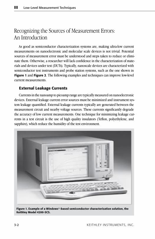
As good as semiconductor characterization systems are, making ultra-low current measurements on nanoelectronic and molecular scale devices is not trivial. Potential sources of measurement error must be understood and steps taken to reduce or elimi-nate them. Otherwise, a researcher will lack confidence in the characterization of mate-rials and devices under test (DUTs). Typically, nanoscale devices are characterized with semiconductor test instruments and probe station systems, such as the one shown in Figure 1 and Figure 2. The following examples and techniques can improve low-level current meas ure ments.
external Leakage Currents
Currents in the nanoamp to picoamp range are typically measured on nanoelectronic devices. External leakage current error sources must be minimized and instrument sys-tem leakage quantified. External leakage currents typically are generated between the measurement circuit and nearby voltage sources. These currents significantly degrade the accuracy of low current measurements. One technique for minimizing leakage cur-rents in a test circuit is the use of high quality insulators (Teflon, polyethylene, and sapphire), which reduce the humidity of the test environment.
Figure 1. example of a Windows®-based semiconductor characterization solution, the Keithley Model 4200-SCS.
iii Low-Level Measurement Techniques
nanotechnology measurement handbooK 3-3
iii
Insulators absorb water vapor from the air, with the amount absorbed dependant on the insulator material and humidity level. When the insulator contains ionic con-taminants, spurious current generation can be especially troublesome in high humidity environments. The best insulator choice is one on which water vapor does not readily form a continuous film. However, this may be unavoidable if the DUT absorbs water easily. In that case, it’s best to make the measurements in an environmentally controlled, low- humidity room.
The use of guarding is a principal method of reducing leakage currents in a test circuit. A guard is a conductor connected to a low impedance point in the circuit that is at nearly the same potential as the high impedance lead being guarded (for exam-ple, In/Out HI in Figure 3). Guarding can isolate the high impedance input lead of an electrometer, picoammeter, or source- measure unit (SMU) from leakage current due to voltage sources. Guarding can also reduce the effect of shunt capacitance in the measurement circuit.
Grounding and Shielding
It is important to distinguish between an instrument’s common and chassis grounds. The common is the ground for the complete measurement circuit; it will affect the system’s low-level measurement performance. In contrast, the chassis ground is con-nected to the power line ground and is mainly used for safety reasons. Usually, there are
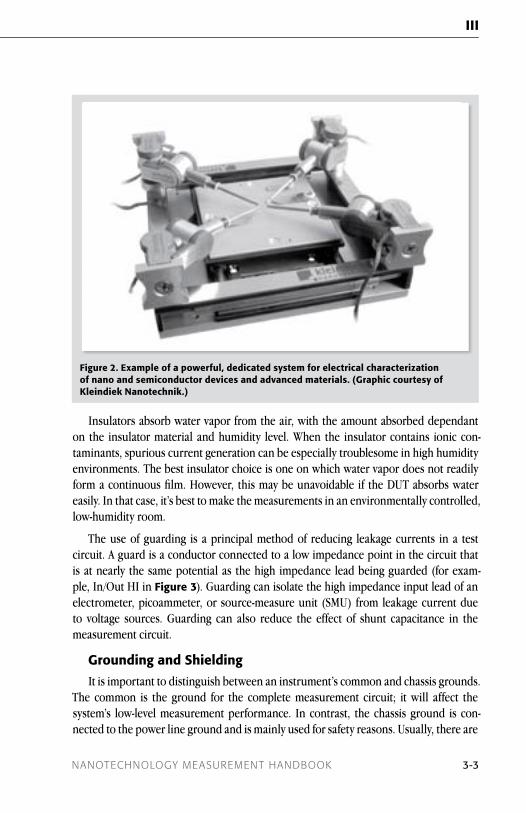
Figure 2. example of a powerful, dedicated system for electrical characterization of nano and semiconductor devices and advanced materials. (Graphic courtesy of Kleindiek nanotechnik.)

3-4 Keithley instruments, inc .
iii Low-Level Measurement Techniques
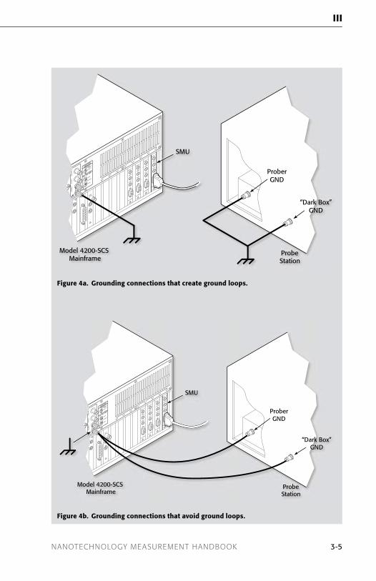
no problems associated with connecting these grounds together. Sometimes, however, the power line ground can be noisy. In other cases, a test fixture and probe station connected to the instrument may create a ground loop that generates additional noise. Accurate low-level measurements require a comprehensive system-grounding plan.
Although grounding and shielding are closely related, they are actually two different issues. In a test fixture or probe station, the DUT and probe typically are enclosed in soft metal shielding. The metal enclosure helps eliminate interference from power lines and high frequency radiation (RF or microwave) and reduces magnetic interference. The metal normally is grounded for safety reasons. However, when an instrument is connected to a probe station through triaxial cables (the type used for guarded connec-tions), physical grounding points are very important.
The configuration in Figure 4a illustrates a common grounding error. Note that the instrument common and the chassis ground are connected. The probe station is also grounded to the power line locally. Even more significant, the measurement instrument and the probe station are connected to different power outlets. The power line grounds of these two outlets may not be at the same electrical potential all the time. Therefore, a
Guard
Local
Remote
Local
Remote
In/Out HI
Sense HI
Sense LO
V Source
In/Out LO
I Meter
Guard Sense
+
–
SenseOutput
AdjustV Source
(Feedback)
V Meter
x1
Figure 3. Simplified block diagram of a source-measure unit (SMU) configured to source voltage and measure current, showing guard connections.
iii Low-Level Measurement Techniques
nanotechnology measurement handbooK 3-5
iii
SMU
Model 4200-SCSMainframe
ProberGND
ProbeStation
“Dark Box”GND
Figure 4a. Grounding connections that create ground loops.
SMU
Model 4200-SCSMainframe
ProberGND
ProbeStation
“Dark Box”GND
Figure 4b. Grounding connections that avoid ground loops.
3-6 Keithley instruments, inc .
iii Low-Level Measurement Techniques
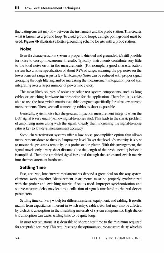
fluctuating current may flow between the instrument and the probe station. This creates what is known as a ground loop. To avoid ground loops, a single point ground must be used. Figure 4b illustrates a better grounding scheme for use with a probe station.
noiseEven if a characterization system is properly shielded and grounded, it’s still possible
for noise to corrupt measurement results. Typically, instruments contribute very little to the total noise error in the measurements. (For example, a good characterization system has a noise specification of about 0.2% of range, meaning the p-p noise on the lowest current range is just a few femtoamps.) Noise can be reduced with proper signal averaging through filtering and/or increasing the measurement integration period (i.e., integrating over a larger number of power line cycles).
The most likely sources of noise are other test system components, such as long cables or switching hardware inappropriate for the application. Therefore, it is advis-able to use the best switch matrix available, designed specifically for ultra-low current measurements. Then, keep all connecting cables as short as possible.
Generally, system noise has the greatest impact on measurement integrity when the DUT signal is very small (i.e., low signal-to-noise ratio). This leads to the classic problem of amplifying noise along with the signal. Clearly then, increasing the signal-to-noise ratio is key to low-level measurement accuracy.
Some characterization systems offer a low noise pre-amplifier option that allows measurements down to the sub-femptoamp level. To get that level of sensitivity, it is best to mount the pre-amps remotely on a probe station platen. With this arrangement, the signal travels only a very short distance (just the length of the probe needle) before it is amplified. Then, the amplified signal is routed through the cables and switch matrix into the measurement hardware.
Settling TimeFast, accurate, low current measurements depend a great deal on the way system
elements work together. Measurement instruments must be properly synchronized with the prober and switching matrix, if one is used. Improper synchronization and source-measure delay may lead to a collection of signals unrelated to the real device parameters.
Settling time can vary widely for different systems, equipment, and cabling. It results mainly from capacitance inherent in switch relays, cables, etc., but may also be affected by dielectric absorption in the insulating materials of system components. High dielec-tric absorption can cause settling time to be quite long.
In most test situations, it is desirable to shorten test time to the minimum required for acceptable accuracy. This requires using the optimum source-measure delay, which is

iii Low-Level Measurement Techniques
nanotechnology measurement handbooK 3-7
iii
a function of the instrumentation source and measurement time, along with the system settling time. The latter usually is the dominant portion of source-measure delay time.
A step voltage test is typically used to characterize system settling time. A 10V step is applied across two open-circuit probe tips, and then current is monitored continuously for a period of time. The resulting current vs. time (I-t) curve (Figure 5) illustrates the transient segment and the steady current segment. Immediately after the voltage step, the transient current will gradually decay to a steady value. The time it takes to reach the steady value is the system settling time. Typically, the time needed to reach 1/e of the initial value is defined as the system time constant.
With the system leakage I-t curve in hand, the next step is to establish the accept-able measurement sensitivity or error. Suppose the task requires accurate DUT leak-age measurements only at the picoamp level. Then, source-measure delay time can be established by a point on the transient portion of the system settling curve (Figure 5) where the leakage current is at a sub-picoamp level. If the expected DUT current is in the femtoamp range, then the delay time must be extended so that the transient current reaches a value lower than the expected reading before a measurement is taken.
System Leakage CurrentOnce the transient current has settled to its steady value, it corresponds to the sys-
tem leakage current. Typically, system leakage current is expressed as amperes per volt.
1e–10
1e–11
1e–12
1e–13
1e–14
1e–15
1e–16
Curr
ent
(Am
ps)
0 .0 0 .5 1 .0 1 .5 2 .0 2 .5 3 .0 3 .5 4 .0
Time (seconds)Step voltage
applied
Figure 5. Use instrument settling time to set source-measure delays. Leakage current (in this case, 10–15A) establishes the limit on basic instrument sensitivity.

3-8 Keithley instruments, inc .
iii Low-Level Measurement Techniques
To determine its magnitude, simply measure the steady-state current and divide by the voltage step value. The magnitude of the system leakage current establishes the noise floor and overall sensitivity of the system. Usually, the largest leakage current contribu-tors are the probe card and switching relays.
extraneous CurrentErrors in current measuring instruments arise from extraneous currents flowing
through various circuit elements. In the current measurement model of Figure 6, the current indicated on the meter (M) is equal to the actual current through the meter (I1), plus or minus the inherent meter uncertainty. I1 is the signal current (IS), less the shunt current (ISH) and the sum of all generated error currents (IE).
error Current ModelFigure 6 identifies the various noise and error currents generated during typical
current measurements, which contribute to the error sum (IE). The ISE current genera-tor represents noise currents produced within the DUT and its voltage source. These currents could arise due to the aforementioned leakage and dielectric absorption, or due to electrochemical, piezoelectric, and triboelectric effects. ICE represents currents generated in the interconnection between the meter and the source/DUT circuit. IIE rep-resents the error current arising from all internal measuring instrument sources. IRE is generated by the thermal activity of the shunt resistance. The rms value of this thermal noise current is given by:
IRE = (4kTf/RSH)1/2
where: k = Boltzman’s constant (1.38 × 10⁻²³J/K) T = Absolute temperature in °K f = Noise bandwidth in Hz RSH = Resistance in ohms
Making the Most of instrumentationMaking accurate low current measurements on nanoelectronic, moletronic (molecu-
lar electronic), and other nanoscale devices demands a thorough analysis of potential error sources, plus steps to reduce possible errors. These steps include selection of ap-propriate grounding and shielding techniques, cables, probe cards, switching matrices, etc. These efforts allow nanotechnology researchers to make the most of the capabili-ties inherent in modern device characterization systems.
Properly applied, these systems can speed up development of CNT and molecular electronic structures, which may ultimately redefine the processes used to fabricate semiconductor devices. By providing a means for economical, massive integration, such technology could pave the way for new computing architectures, 100× speed increases, significant reduction in power consumption, and other breakthroughs in performance.

iii Low-Level Measurement Techniques
nanotechnology measurement handbooK 3-9
iii
RSHV ISEISE ICE IRE IIE
I1 I1 = IS – ISH – IE
IE = ISE + ICE + IRE + IIECurrent Source
IS
ISI SEICE
===
Source currentSource noise currentInterconnection noise current
RSHIREIIE
===
Shunt resistanceShunt resistance noiseInstrument error current
I SH
M
Figure 6. Source of current error in a Shunt Type Ammeter.

3-10 Keithley instruments, inc .
iii Low-Level Measurement Techniques
Examples of Low Current Measurements on Nanoelectronic and Molecular Electronic Devices
nanotech developmentMoore’s Law states that circuit density will double every 18 months. However, in
order to maintain this rate of increase, there must be fundamental changes in the way circuits are formed. Over the past few years, there have been significant and exciting developments in nanotechnology, particularly in the areas of nanoelectronics and mo-lecular electronic (also called moletronic) devices.
As is well known, Moore’s Law within the semiconductor industry is being chal-lenged even further as devices continue to shrink down to molecular levels. These new nanoelectronic devices require careful characterization and well thought out manu-facturing processes in order for commercialization to take place. Thus, professional organizations such as IEEE and SEMI (Semiconductor Equipment and Materials Interna-tional) are collaborating to develop the next generation of measurement and metrology standards for the industry.
Below a semiconductor scale of 100nm, the principles, fabrication methods, and ways to integrate silicon devices into systems are quite different, but apparently not impossible. Still, the increasing precision and quality control required for silicon devices smaller than 100nm will presumably require new fabrication equipment and facilities that may not be justified due to high cost. Even if cost were not a factor, silicon devices have physical size limitations that affect their performance. That means the race is on to develop nano dimen sional devices and associated production methods.
Carbon nanotube and organic Chain devicesTwo types of molecules that are being used as current carrying, nano-scale elec-
tronic devices are carbon nanotubes and polyphenylene-based chains. Researchers have already demonstrated carbon nanotube based FETs, nanotube based logic inverters, and organic-chain diodes, switches, and memory cells. All of these can lead to early stage logic devices for future computer architectures.
Carbon nanotubes (CNTs) have unique properties that make them good candidates for a variety of electronic devices. They can have either the electrical conductivity of metals or act as a semiconductor. (Controlling CNT production processes to achieve the desired property is a major area of research.) CNT current carrying densities are as high as 109A/cm2, whereas copper wire is limited to about 106A/cm2. Besides acting as current conductors to interconnect other small-scale devices, CNTs can be used to construct a number of circuit devices. Researchers have experimented with CNTs in the fabrication of FETs, FET voltage inverters, low temperature single-electron transistors, intramolecu-lar metal-semiconductor diodes, and intermolecular-crossed NT-NT diodes [1].

iii Low-Level Measurement Techniques
nanotechnology measurement handbooK 3-11
iii
The CNT FET uses a nanotube that is laid across two gold contacts that serve as the source and drain, as shown in Figure 1a. The nanotube essentially becomes the current carrying channel for the FET. DC characterization of this type of device is carried out just as with any other FET. An example is shown in Figure 1b.
Figure 1b shows that the amount of current (ISD) flowing through a nanotube chan-nel can be changed by varying the voltage applied to the gate (VG) [2]. Other tests typi-cally performed on such devices include a transconductance curve (upper right corner of Figure 1b), gate leakage, leakage current vs. temperature, substrate to drain leakage, and sub-threshold current. Measurements that provide insight into fundamental proper-ties of conduction, such as transport mechanisms and I-V vs. temperature are critical.
Gate Oxide
GateNanotube
Source Drain
Silicon DioxideSilicon Wafer
© IBM
Figure 1a. Schematic cross-section of iBM’s CnFeT (carbon nanotube field effect transistor).
Figure 1b. iSd versus VG for an iBM nanotube FeT [2]. The different plots represent different source-drain voltages. iBM Copyright
3-12 Keithley instruments, inc .
iii Low-Level Measurement Techniques
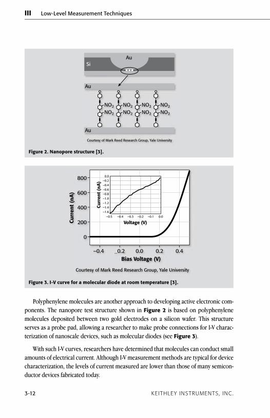
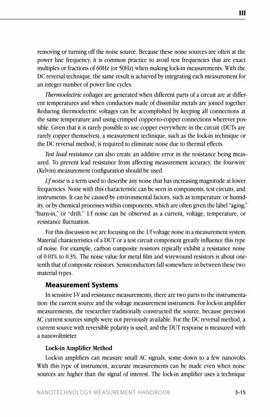
Polyphenylene molecules are another approach to developing active electronic com-ponents. The nanopore test structure shown in Figure 2 is based on polyphenylene molecules deposited between two gold electrodes on a silicon wafer. This structure serves as a probe pad, allowing a researcher to make probe connections for I-V charac-terization of nanoscale devices, such as molecular diodes (see Figure 3).
With such I-V curves, researchers have determined that molecules can conduct small amounts of electrical current. Although I-V measurement methods are typical for device characterization, the levels of current measured are lower than those of many semicon-ductor devices fabricated today.
NO2
NO2
NO2
NO2
NO2
NO2
NO2
NO2
Au
Au
AuSi
Courtesy of Mark Reed Research Group, Yale University
Figure 2. nanopore structure [3].
800
600
400
200
0
Curr
ent
(nA
)
–0 .4 _0 .2 0 .0 0 .2 0 .4Bias Voltage (V)
Courtesy of Mark Reed Research Group, Yale University
0 .0–0 .2–0 .4–0 .6–0 .8–1 .0–1 .2–1 .4–1 .6
–0 .5 –0 .4 –0 .3 –0 .2 –0 .1 0 .0
Voltage (V)
Curr
ent
(nA
)
Figure 3. i-V curve for a molecular diode at room temperature [3].

iii Low-Level Measurement Techniques
nanotechnology measurement handbooK 3-13
iii
I-V characterization of moletronic devices requires low level current measurements in the nanoamp to femtoamp range. To complicate matters, these measurements are quite often made at cryogenic temperatures. Therefore, highly sensitive instruments are required, and appropriate measurement and connection techniques must be employed to avoid errors. Typically, nanoelectronic and moletronic devices are characterized with semiconductor test instruments and probe station systems, such as the one shown in Figure 4.
References[1] Yi Cui, Charles Lieber, “Functional Nanoscale Electronic Devices Assembled Using Silicon
Building Blocks,” Science, vol. 291, pp. 851-853, Jan. 2, 2002.
[2] Nanoscale Science Department. (2001, October 1). Nanotube field-effect transistor. IBM T. J. Watson Research Center, Yorktown Heights, NY. [Online]. Available: http://www .research .ibm .com/nanoscience/fet .html
[3] Mark A. Reed Research Group. (2002, April 18). Molecular Electronic Devices. Yale Univer-sity. New Haven, CT. Available at: http://www .eng .yale .edu/reedlab/research/device/mol_devices .html
Figure 4. example of a Windows®-based semiconductor characterization system, the Keithley Model 4200-SCS.

3-14 Keithley instruments, inc .
iii Low-Level Measurement Techniques
AC versus DC Measurement Methods for Low Power Nanotech and Other Sensitive Devices
Sensitive Measurement needsResearchers today must measure material and device characteristics that involve
very small currents and voltages. Examples include the measurement of resistance and I-V characteristics of nanowires, nanotubes, semiconductors, metals, superconductors, and insulating materials. In many of these applications, the applied power must be kept low in order to avoid heating the device under test (DUT), because (1) the DUT is very small and its temperature can be raised significantly by small amounts of applied power, or (2) the DUT is being tested at temperatures near absolute zero where even a milli-degree of heating is not acceptable. Even if applied power is not an issue, the measured voltage or current may be quite small due to extremely low or high resistance.
Measurement Techniques and error SourcesThe key to making accurate low power measurements is minimizing the noise. In
many low power measurements, a common technique is to use a lock-in amplifier to apply a low level AC current to the DUT and measure its voltage drop. An alternative is to use a DC current reversal technique. In either case, a number of error sources must be considered and controlled.
Johnson noise places a fundamental limit on resistance measurements. In any re-sistance, thermal energy produces the motion of charged particles. This charge move-ment results in Johnson noise. It has a white noise spectrum and is determined by the temperature, resistance, and frequency bandwidth values. The formula for the voltage noise generated is:
VJohnson (rms) = √4kTRB
where: k = Boltzmann’s constant (1.38 × 10⁻²³ J/K) T = Absolute temperature in degrees Kelvin R = DUT resistance in Ω B = Noise bandwidth (measurement bandwidth) in Hz
Johnson noise may be reduced by:
• Reducing bandwidth with digital filtering (averaging readings) or analogfiltering
• Reducingthetemperatureofthedevice
• Reducingthesourceresistance
External noise sources are interferences created by motors, computer screens, or other electrical equipment. They can be controlled by shielding and filtering or by
iii Low-Level Measurement Techniques
nanotechnology measurement handbooK 3-15
iii
removing or turning off the noise source. Because these noise sources are often at the power line frequency, it is common practice to avoid test frequencies that are exact multiples or fractions of 60Hz (or 50Hz) when making lock-in measurements. With the DC reversal technique, the same result is achieved by integrating each measurement for an integer number of power line cycles.
Thermoelectric voltages are generated when different parts of a circuit are at differ-ent temperatures and when conductors made of dissimilar metals are joined together. Reducing thermoelectric voltages can be accomplished by keeping all connections at the same temperature and using crimped copper-to-copper connections wherever pos-sible. Given that it is rarely possible to use copper everywhere in the circuit (DUTs are rarely copper themselves), a measurement technique, such as the lock-in technique or the DC reversal method, is required to eliminate noise due to thermal effects.
Test lead resistance can also create an additive error in the resistance being meas-ured. To prevent lead resistance from affecting measurement accuracy, the four-wire (Kelvin) measurement configuration should be used.
1/f noise is a term used to describe any noise that has increasing magnitude at lower frequencies. Noise with this characteristic can be seen in components, test circuits, and instruments. It can be caused by environmental factors, such as temperature or humid-ity, or by chemical processes within components, which are often given the label “aging,”
“burn-in,” or “drift.” 1/f noise can be observed as a current, voltage, temperature, or resistance fluctuation.
For this discussion we are focusing on the 1/f voltage noise in a measurement system. Material characteristics of a DUT or a test circuit component greatly influence this type of noise. For example, carbon composite resistors typically exhibit a resistance noise of 0.01% to 0.3%. The noise value for metal film and wirewound resistors is about one-tenth that of composite resistors. Semiconductors fall somewhere in between these two material types.
Measurement SystemsIn sensitive I-V and resistance measurements, there are two parts to the instrumenta-
tion: the current source and the voltage measurement instrument. For lock-in amplifier measurements, the researcher traditionally constructed the source, because precision AC current sources simply were not previously available. For the DC reversal method, a current source with reversible polarity is used, and the DUT response is measured with a nanovoltmeter.
Lock-in Amplifier Method
Lock-in amplifiers can measure small AC signals, some down to a few nanovolts. With this type of instrument, accurate measurements can be made even when noise sources are higher than the signal of interest. The lock-in amplifier uses a technique

3-16 Keithley instruments, inc .
iii Low-Level Measurement Techniques
called phase sensitive detection to single out the signal at a specific test frequency. Noise signals at other frequencies are largely ignored. Because the lock-in amplifier only mea-sures AC signals at or near the test frequency, the effects of thermoelectric voltages (both DC and AC) are also reduced.
Figure 1 is a simplified block diagram of a lock-in amplifier setup to measure the voltage of a DUT at low power. Current is forced through the DUT by applying a sinu-soidal voltage (Asin[2π fot]) across the series combination of RREF and the DUT. Usually, RREF is chosen to be much larger than the DUT resistance, thereby creating an approxi-mate current source driving the DUT.
RREF
+
–
DUTAsin(2π· fo · t)
LowPassFilter
LowPassFilter
cos(2π· fo · t)
sin(2π· fo · t)
Voltage(Real)
Voltage(Imaginary)
Figure 1. Simplified block diagram of a lock-in amplifier measurement setup.
The amplified voltage from the DUT is multiplied by both a sine and a cosine wave with the same frequency and phase as the applied source and then put through a low pass filter. This multiplication and filtering can be done with analog circuits, but to-day they are more commonly performed digitally within the lock-in amplifier after the DUT’s response signal is digitized.
The outputs of the low pass filters are the real (in phase) and imaginary (out of phase) content of the voltage at the frequency fo. DUT resistance values must be calcu-lated separately by the researcher based on the assumed current and measured voltage levels.
Researchers using lock-in amplifiers often choose to operate the instrument at a rela-tively low frequency, i.e., less than 50Hz. A low frequency is chosen for many reasons. These include (1) getting far enough below the frequency roll-off of the DUT and inter-connects for an accurate measurement, (2) avoiding noise at the power line frequency, and (3) getting below the frequency cutoff of in-line electromagnetic interference (EMI) filters added to keep environmental noise from reaching the DUT.
DC Reversal Measurement Method
An alternative to lock-in amplifiers uses DC polarity reversals in the applied current signal to nullify noise. This is a well-established technique for removing offsets and low frequency noise. Today’s DC sources and nanovoltmeters offer significant advantages
iii Low-Level Measurement Techniques
nanotechnology measurement handbooK 3-17
iii
over lock-in amplifiers in reducing the impact of error sources and reduce the time required to achieve a low noise measurement.
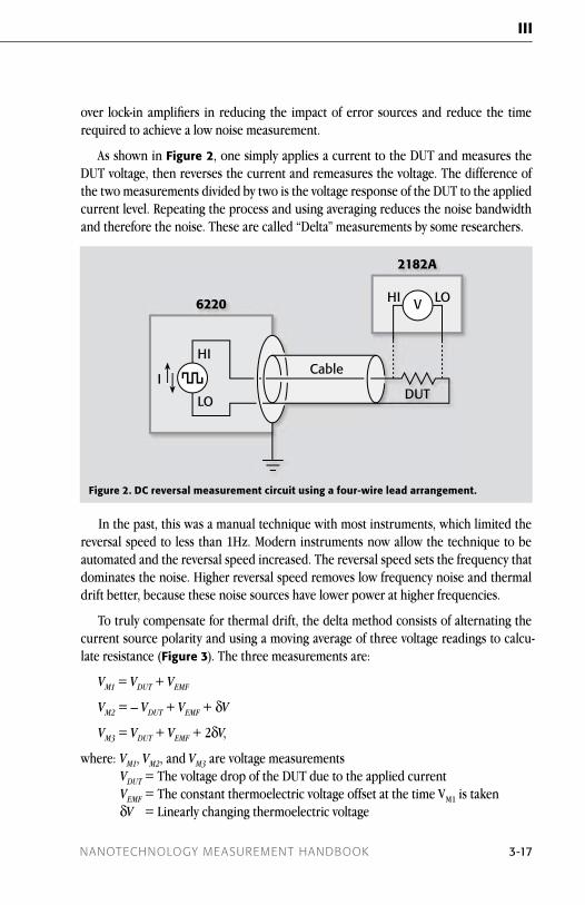
As shown in Figure 2, one simply applies a current to the DUT and measures the DUT voltage, then reverses the current and remeasures the voltage. The difference of the two measurements divided by two is the voltage response of the DUT to the applied current level. Repeating the process and using averaging reduces the noise bandwidth and therefore the noise. These are called “Delta” measurements by some researchers.
I
HI
LO
Cable
DUT
VHI LO6220
2182A
Figure 2. dC reversal measurement circuit using a four-wire lead arrangement.
In the past, this was a manual technique with most instruments, which limited the reversal speed to less than 1Hz. Modern instruments now allow the technique to be automated and the reversal speed increased. The reversal speed sets the frequency that dominates the noise. Higher reversal speed removes low frequency noise and thermal drift better, because these noise sources have lower power at higher frequencies.
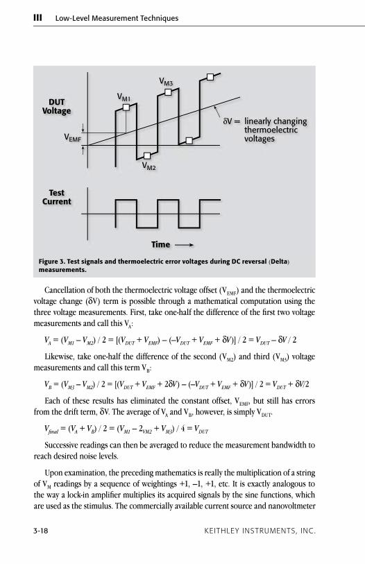
To truly compensate for thermal drift, the delta method consists of alternating the current source polarity and using a moving average of three voltage readings to calcu-late resistance (Figure 3). The three measurements are:
VM1 = VDUT + VEMF
VM2 = – VDUT + VEMF + δV
VM3 = VDUT + VEMF + 2δV,
where: VM1, VM2, and VM3 are voltage measurementsVDUT = The voltage drop of the DUT due to the applied currentVEMF = The constant thermoelectric voltage offset at the time VM1 is takenδV = Linearly changing thermoelectric voltage
3-18 Keithley instruments, inc .
iii Low-Level Measurement Techniques
Cancellation of both the thermoelectric voltage offset (VEMF) and the thermoelectric voltage change (δV) term is possible through a mathematical computation using the three voltage measurements. First, take one-half the difference of the first two voltage measurements and call this VA:
VA = (VM1 – VM2) / 2 = [(VDUT + VEMF) – (–VDUT + VEMF + δV)] / 2 = VDUT – δV / 2
Likewise, take one-half the difference of the second (VM2) and third (VM3) voltage measurements and call this term VB:
VB = (VM3 – VM2) / 2 = [(VDUT + VEMF + 2δV) – (–VDUT + VEMF + δV)] / 2 = VDUT + δV/2
Each of these results has eliminated the constant offset, VEMF, but still has errors from the drift term, δV. The average of VA and VB, however, is simply VDUT.
Vfinal = (VA + VB) / 2 = (VM1 – 2VM2 + VM3) / 4 = VDUT
Successive readings can then be averaged to reduce the measurement bandwidth to reach desired noise levels.
Upon examination, the preceding mathematics is really the multiplication of a string of VM readings by a sequence of weightings +1, –1, +1, etc. It is exactly analogous to the way a lock-in amplifier multiplies its acquired signals by the sine functions, which are used as the stimulus. The commercially available current source and nanovoltmeter
DUTVoltage
TestCurrent
Time
VEMF
VM1
VM3
VM2
δV = linearly changingthermoelectricvoltages
Figure 3. Test signals and thermoelectric error voltages during dC reversal (delta) measurements.

iii Low-Level Measurement Techniques
nanotechnology measurement handbooK 3-19
iii
described in the endnote of this discussion automate the entire procedure; resistance values are calculated and displayed by the instrumentation.
Same Technique, Improved Measurement Hardware
As we’ve seen, the lock-in amplifier method and DC reversal method are both AC measurements. In both methods, DC noise and the noise at higher frequencies are rejected. However, the nanovoltmeter/current source combination can provide superior measurement capabilities over the entire range of device resistances, as explained in the following paragraphs.
Measurements on Low Resistance dUTs
A typical low resistance measurement application is shown in Figure 4. Instrument voltage noise is generally the dominant error in low resistance measurements, but be-low a certain level of device resistance, common mode noise becomes a problem.
HI
LO
RDUT
RLEAD RLEAD
Circuit Node A
VM
HI
LO
ITESTITEST
Figure 4. Block diagram of a typical low resistance measurement.
The four lead resistances shown in Figure 4 vary from 0.1Ω to 100Ω, depending on the experiment. They are important to note, because with low resistance devices, even the impedance of copper connection wires can become large compared to the DUT resistance. Further, in the case of many low impedance experiments carried out at low temperatures, there are often RF filters (e.g., Pi filters) in each of the four device connection leads, typically having 100Ω of resistance.
Regardless of the instruments used to carry out the AC measurements, the test cur-rent flows through the source connection leads and develops a voltage drop from the circuit ground to the connection to the DUT, denoted as Circuit Node A. Thus, the volt-age at circuit node A moves up and down with an amplitude of ITEST × RLEAD volts, while the VMEASURE input is trying to detect a much smaller AC voltage of ITEST × RDUT.
With the connections in this type of measurement circuit, common mode rejection ratio (CMRR) becomes an issue. CMRR specifies how well an instrument can reject variations in the measurement LO potential. The CMRR specification for a typical lock-in amplifier is 100dB (a factor of 105 rejection). In actual measurement practice, this is

3-20 Keithley instruments, inc .
iii Low-Level Measurement Techniques
more likely to fall in the range of 85–90dB. By comparison, nanovoltmeters are avail-able with CMRR specifications of 140dB. Combined with a modern current source op-erating in delta mode, it is possible to achieve a CMRR of better than 200dB in actual measurements.
To understand the impact of CMRR, consider the example described previously. With only 100dB rejection, the measurement of VDUT (which should be ITEST × RDUT) is in fact ITEST × RDUT ± ITEST × RLEAD/105. Thus, there is a 1% error when RLEAD is 103 × RDUT. With 100Ω lead resistance, it is impossible to make a measurement within ±1% error bounds when RDUT is less than 0.1Ω. On the other hand, a modern DC current source and nanovoltmeter, with their combined CMRR of greater than 200dB, can measure resistances as low as 1µΩ within ±1% error bounds, even with a 100Ω lead resistance.
VM
HI
LO
Cable
DUT
VS
HI
LO
Cable R = user supplied resistor
Lock-In
Figure 5. Making a “current source” from a lock-in amplifier.
It is also worth noting that in the case of the lock-in amplifier, the current source shown in Figure 4 would likely be a homemade source constructed from the VOUTPUT and a hand-selected (and thoroughly characterized) resistor (R), as shown in Figure 5. Every time a different test current is desired, a new resistor must be characterized, inserted in the circuit, temperature stabilized, and shielded. Even with this effort, it does not deliver constant current, but instead varies as the DUT resistance varies. Now, commercial reversible DC current sources provide stable outputs that are far more pre-dictable without manual circuit adjustments to control current magnitude.
High Resistance MeasurementsValues of DUT resistance greater than 10kΩ present challenges of current noise
and input loading errors. Current noise becomes visible as a measured voltage noise

iii Low-Level Measurement Techniques
nanotechnology measurement handbooK 3-21
iii
that scales with the DUT resistance. In both the lock-in amplifier and the DC reversal systems, current noise comes from the measurement circuit and creates additional AC and DC voltage as it flows through the DUT and/or lead resistance.
For both types of systems, noise values can be of a similar magnitude. A typical value is 50pA DC with 80fA/√Hz noise for the reversible current source/nanovolt meter combi-nation. For a lock-in amplifier, it would be around 50pA DC with 180fA/√Hz noise. While the 50pA DC does not interfere with the AC measurements, it does add power to the DUT and must be counted in the total power applied to the DUT by the measurement system. This presents a much smaller problem for the DC reversal measurement system, because a programmable current source can easily be made to add a DC component to the sourced current to cancel out the DC current emanating from the nanovoltmeter. The lock-in amplifier does not have this capability.
The second limitation in measuring higher DUT resistances is the input impedance of the voltage measuring circuit, which causes loading errors. Consider the measurement of a DUT with 10MΩ of resistance. A typical lock-in amplifier has an input impedance of about the same magnitude—10MΩ. This means that half of the current intended for the DUT will instead flow through the instrument input, and the measured voltage will be in error by 50%. Even with careful subtraction schemes, it is not practical to achieve ±1% accuracy when measuring a DUT with a resistance greater than 1MΩ when using a lock-in amplifier.
By contrast, a nanovoltmeter has 1000 times higher input impedance (i.e., 10GΩ), so it can measure up to 1GΩ with ±1% accuracy. (Subtracting the loading effect of the 10GΩ only requires knowing the input resistance to ±10% accuracy, which is readily measured by performing the DC reversal measurement using an open circuit as the
“DUT.”) Moreover, some current sources provides a guard amplifier, so the nanovolt-meter can measure the guard voltage instead of the DUT voltage directly (Figure 6). This reduces the current noise transmitted to the DUT down to the noise of the cur-rent source (below 20fA/√Hz). This configuration reduces the loading error, noise, and power in situations where the lead resistance is negligible and a two-wire connection to the DUT is acceptable.
Mid-range Resistance Measurements
Traditionally, lock-in amplifiers have been used for measurements in the range of 100mΩ to 1MΩ due to the significant limitations outside this range. Even when RDUT falls in this range, using the DC reversal method with newer instruments may provide an advantage. For example, a lock-in amplifier has two times (or higher) white noise than a modern DC reversal system, and its 1/f voltage noise is ten times higher. (See Figure 7.) For example, when working at 13Hz (a typical frequency in lock-in measurements),

3-22 Keithley instruments, inc .
iii Low-Level Measurement Techniques
1E–7
1E–8
1E–91 10 100 1000
Frequency (Hz)
Lock-in amplifier
Model 6221/2182A
Figure 7. noise comparison of a typical lock-in amplifier and dC reversal measurement system. (See endnote on instruments used for comparisons.)
×1
I
HI
LO
Cable
dUT
V
HI
LO
6221 2182A
GUARD
LO
Figure 6. Test arrangement for a two-wire dC reversal measurement using a current source with a guard buffer circuit. (Guarded source connections provide a way around the problems associated with the low input impedance of a measurement circuit.)

iii Low-Level Measurement Techniques
nanotechnology measurement handbooK 3-23
iii
a typical DC reversal system has about seven times lower voltage noise than a lock-in amplifier. This leads to 50 times less required power.
individual instrument noise Comparisons
All electronic circuits generate both white noise and 1/f noise. The noise of low fre-quency measurements are often dominated by the latter. A lock-in amplifier’s front end is usually the dominant source of 1/f noise. Instruments used in the DC reversal method have similar issues. Therefore, comparing the noise performance of a lock-in amplifier with an instrument using the DC reversal method is essentially a case of comparing the noise performance of their front-end circuitry. Furthermore, the DUT resistance value must be considered when making these comparisons.
It is common for manufacturers to specify their white noise performance, but less common to be given a 1/f noise specification. To make a valid comparison, like the one in Figure 7, the noise level should be determined as measurements are made. Another important consideration is whether to use the system voltage noise or current noise. Figure 8 shows a model of a measurement system with Vn being the voltage noise of the system, In being the current noise, and IS being the source current.
RDUT IS (ideal) IdealDVM
Vn
In
Measurement System Model
Figure 8. idealized measurement circuit with current and voltage noise sources, in and Vn.
A signal-to-noise ratio of one (one possible measurement objective) is achieved when the power forced on the DUT equals the noise power of the system. This is expressed by:
PDUT = I2S · RDUT = V2
n / RDUT + I2n · RDUT
This equation describes the V-shaped curves in Figure 9. Voltage noise dominates when the DUT resistance is low, and current noise dominates when the DUT resistance is high. The required power is minimum when RDUT equals Vn/In. Ultimately, a major determinant of instrument performance is how little power can be imposed on the DUT and still get a good measurement. Nevertheless, it is important to remember that very low and very high values of RDUT impose different types of instrument limitations on these measurements compared to midrange values.
3-24 Keithley instruments, inc .
iii Low-Level Measurement Techniques
noise, Applied power, and Measurement Time Considerations
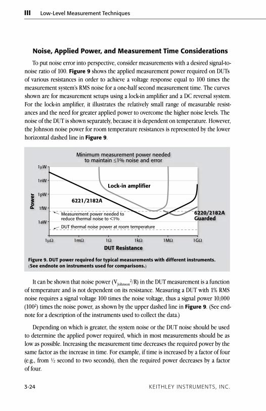
To put noise error into perspective, consider measurements with a desired signal-to-noise ratio of 100. Figure 9 shows the applied measurement power required on DUTs of various resistances in order to achieve a voltage response equal to 100 times the measurement system’s RMS noise for a one-half second measurement time. The curves shown are for measurement setups using a lock-in amplifier and a DC reversal system. For the lock-in amplifier, it illustrates the relatively small range of measurable resist-ances and the need for greater applied power to overcome the higher noise levels. The noise of the DUT is shown separately, because it is dependent on temperature. However, the Johnson noise power for room temperature resistances is represented by the lower horizontal dashed line in Figure 9.
dUT Resistance1µΩ 1mΩ 1Ω 1kΩ 1MΩ 1GΩ
1µW
1nW
1pW
1fW
1aW
pow
er
Minimum measurement power neededto maintain ≤1% noise and error
6221/2182A
Lock-in amplifier
6220/2182AGuarded
Measurement power needed toreduce thermal noise to <1%
DUT thermal noise power at room temperature
Figure 9. dUT power required for typical measurements with different instruments. (See endnote on instruments used for comparisons.)
It can be shown that noise power (VJohnson2/R) in the DUT measurement is a function
of temperature and is not dependent on its resistance. Measuring a DUT with 1% RMS noise requires a signal voltage 100 times the noise voltage, thus a signal power 10,000 (1002) times the noise power, as shown by the upper dashed line in Figure 9. (See end-note for a description of the instruments used to collect the data.)
Depending on which is greater, the system noise or the DUT noise should be used to determine the applied power required, which in most measurements should be as low as possible. Increasing the measurement time decreases the required power by the same factor as the increase in time. For example, if time is increased by a factor of four (e.g., from ½ second to two seconds), then the required power decreases by a factor of four.
iii Low-Level Measurement Techniques
nanotechnology measurement handbooK 3-25
iii
For the current source and nanovoltmeter combination, Figure 9 shows that the system noise is less than the Johnson noise of room temperature DUTs between 500Ω and 100MΩ. Physics present the only limitation on this DC reversal system, and low temperature measurements will benefit from the full capabilities of the system to make measurements with even less power.
SummaryLock-in amplifiers are useful for many measurement applications. Still, their com-
mon mode rejection ratio and low input impedance limits low power resistance meas-ure ments to a range of about 100mΩ to 1MΩ. Typically, they are employed with user constructed current sources, which are difficult to control with variable loads, resulting in poor source accuracy. Results are obtained as current and voltage readings, requiring the researcher to calculate resistance.
With modern current sources and nanovoltmeters, the DC reversal method requires less power while providing excellent low-noise results. This combination is optimal for low frequencies (0.1–24Hz), allowing measurements to be made much faster than with a lock-in amplifier. At resistances less than 100mΩ, they have much better rejection of lead resistances, and, at resistances greater than 1MΩ, they have much higher input impedance and less associated loading error.
The greatest advantage comes from current sources and nanovoltmeters that have been designed to work together in Delta Mode and provide resistance values read directly from the instrument display. These instruments are connected by a communi-cation path that synchronizes them, allowing current reversal frequencies up to about 24Hz. Working as a system, they effectively cancel thermoelectric offsets that drift over time and avoid errors associated with common mode rejection problems that are preva-lent in low impedance measurements. By following good test practices, these instru-ments provide excellent measurement accuracy from 10nΩ to 1GΩ. The measurement noise level for such a system is about 3nV/√Hz at 5Hz and higher frequencies.
endnoteIn Figures 7 and 9, a lock-in amplifier similar to the SR-830 was used to collect data for
comparison with the DC reversal method, the latter using a combination of the Keithley Model 6221 AC and DC Current Source and Model 2182A Nanovoltmeter.
3-26 Keithley instruments, inc .
iii Low-Level Measurement Techniques
Achieving Accurate and Reliable Resistance Measurements in Low Power and Low Voltage Applications
Low voltage measurements are often associated with resistance measurements of highly conductive semiconductor materials and devices. These tests normally involve sourcing a known current, measuring the resulting voltage, and calculating the resist-ance using Ohm’s Law. Because of the DUT’s typically low resistance, the resulting volt-age will be very small and great care needs to be taken to reduce offset voltage and noise, which can normally be ignored when measuring higher signal levels.
However, low voltage measurements can also result from resistance measurements of non-conductive materials and components. Electronics are continuing to shrink as consumers demand faster, more feature-rich products in ever-smaller form factors. Be-cause of their small sizes, electronic components of today usually have limited power handling capability. As a result, when electrically characterizing these components, the test signals need to be kept small to prevent component breakdown or other damage.
In resistance measurements, even if the resistance is far from zero, the voltage to be measured is often very small due to the need to source only a small current. There-fore, low level voltage measurement techniques become important, not only for low resistance measurements, but also for resistance measurements of non-conductive ma-terials and components. For researchers and electronics industry test engineers, this power limitation often makes characterizing the resistance of modern devices and materials challenging.
There are many factors that make low voltage measurements difficult. Various noise sources can make it difficult to resolve the actual voltage. In addition, thermoelectric voltages (thermoelectric EMFs) can cause error offsets and drift in the voltage readings. As mentioned previously, test requirements may limit the maximum current that can be applied, so simply increasing the sourced signal (test current) isn’t always an option. In other cases, increasing the test current could cause device heating, which can change the DUT’s resistance and possibly destroy the DUT. The key to obtaining accurate, con-sistent measurements is eliminating factors that contribute to measurement error. For low voltage measurement applications, such error is composed largely of white noise (random noise across all frequencies) and 1/f noise. Thermoelectric voltages (typically having 1/f distribution), a serious problem in many test environments, are generated from temperature differences in the circuit.
This discussion reviews techniques to eliminate thermoelectric voltages to allow more accurate resistance measurements, including a three-step delta measurement method for low power/low voltage applications.

iii Low-Level Measurement Techniques
nanotechnology measurement handbooK 3-27
iii
Measurement obstacles
Temperature fluctuations are the biggest enemy of low voltage measurements. Any junction of dissimilar metals in a measurement circuit constitutes a thermocouple. Voltage errors occur when there is an opposing junction at a different temperature. Figure 1 illustrates one example of this error.
In this example, the device under test is located on a silicon wafer. A tungsten probe makes contact with one terminal of the device. The other terminal is the silicon sub-strate. A copper base is used to make electrical contact with the substrate. The junctions of differing materials produce three separate thermocouples: at the copper-tungsten interface, at the tungsten-silicon interface, and at the silicon-copper interface. The tem-perature difference between the two materials at each junction generates a voltage at the voltmeter terminals. The summation of the thermoelectric voltages at each of these junctions is the total error voltage that appears at the voltmeter terminals.
The first step toward reducing measurement error is minimizing the temperature variation in the test environment. This would mean reducing the temperature differ-ence between T1, T2, and T3 in Figure 1. The test setup should be isolated from drafts, air conditioning, and heat sources. The connections should be located as close to each other as possible to minimize temperature differences. Whenever possible, the designer of the setup should use connections made of the same material and select insulators with high thermal conductivity to surround the cables and junctions.
Traditional Resistance Measurements
No matter what steps are taken to minimize temperature problems, it’s virtually impossible to eliminate them entirely. A standard DC resistance measurement approach doesn’t compensate for any of these errors. Resistance is calculated using Ohm’s Law; that is, to find the resistance, divide the DC voltage measured across the device by
Cu
Cu
Cu
Thermocouple #1 Cu-W@ T1
Thermocouple 2 W-Si@ T2
W (probe tip )
Thermocouple #3 Si-Cu@ T3
#
VoltmeterTerminals
Si
Figure 1. Typical thermocouple scenario. Cu-Si interface where one terminal is one device on wafer and the second terminal is at the substrate connection to a conductive base.

3-28 Keithley instruments, inc .
iii Low-Level Measurement Techniques
the DC stimulus current (see Figure 2a). The voltage readings will be a sum of the induced voltage across the device (VR), lead and contact resistance (Vlead res), the volt-ages present from the thermals (Vt), other 1/f noise contributions (V1/f noise), and white noise (Vwhite noise). To eliminate lead resistance, use four separate leads to connect the voltmeter and current source to the device. In this way, the voltmeter won’t measure any voltage drop across the source leads. However, the errors due to white noise, 1/f noise, and temperature differences will remain (see Figure 2b). Implementing filtering and selecting the appropriate test equipment may reduce white noise and 1/f noise significantly. However, these elements often determine the measurement noise floor. Temperature presents a slightly different challenge because if the temperature changes, the contribution of the Vt term changes, too. With rapidly changing thermoelectric volt-ages, this term may even exceed VR, the voltage across the DUT induced by the stimulus. It’s possible to reduce thermoelectric voltages using techniques such as all-copper cir-cuit construction, thermal isolation, precise temperature control, and frequent contact cleaning. However, it would be preferable to have a method that would allow accurate resistance measurements even in the presence of large thermoelectric voltages, instead of working to minimize them.
The delta Method of Measuring Resistance
A change in test method is required to improve accuracy and overcome measure-ment obstacles. A constant thermoelectric voltage may be canceled using voltage meas-urements made at a positive test current and a negative test current. This is called a delta reading. Alternating the test current also increases white noise immunity by increasing the signal-to-noise ratio.1 A similar technique can be used to compensate for changing
1 For more details, refer to the “Reducing Resistance Measurement Uncertainty: DC Current Reversals vs. Classic Offset Compensation” white paper on www .keithley .com.
Rlead
Rlead
Vmeasured =VR + Vlead res + Vt +Vwhite noise + V1/f noise
R
Rlead
Rlead
Vmeasured =VR + Vt +Vwhite noise +V1/f noise
R
Multimeter/Ohmmeter
CurrentSource Voltmeter Current
Source Voltmeter
Figure 2a. Figure 2b.
Figure 2. The delta Method of Measuring Resistance: The schematic on the left shows a standard dC resistance measurement setup. Changing the standard measurement setup to the schematic on the right by using four leads eliminates errors due to lead resistance.

iii Low-Level Measurement Techniques
nanotechnology measurement handbooK 3-29
iii
thermoelectric voltages (see Figure 3). Over the short term, thermoelectric drift may be approximated as a linear function (see inset of Figure 3). The difference between consecutive voltage readings is the slope–the rate of change in thermoelectric voltage. This slope is constant, so it may be canceled by alternating the current source three times to make two delta measurements – one at a negative-going step and one at a positive-going step. In order for the linear approximation to be valid, the current source must alternate quickly and the voltmeter must make accurate voltage measurements within a short time interval. If these conditions are met, the three-step delta technique yields an accurate voltage reading of the intended signal unimpeded by thermoelectric offsets and drifts.
Examining this technique in detail reveals how it reduces measurement error. An analysis of the mathematics for one three-step delta cycle will demonstrate how the technique compensates for the temperature differences in the circuit. Consider the ex-ample in Figure 4a:
Test current = ±10nADevice = 100Ω resistorIgnoring thermoelectric voltage errors, the voltages measured at each of the steps
are:V1 = 1µVV2 = –1µVV3 = 1µV
Let’s assume the temperature is linearly increasing over the short term in such a way that it produces a voltage profile like that shown in Figure 4b, where Vt = 100nV and is climbing 100nV with each successive reading.
Thermal Voltage plot
0 .00
5 .00
10 .00
15 .00
20 .00
25 .00
30 .00
Volt
age
(µV)
Figure 3. Thermoelectric drift approximated as a linear function.

3-30 Keithley instruments, inc .
iii Low-Level Measurement Techniques
As Figure 4b shows, the voltages now measured by the voltmeter include error due to the increasing thermoelectric voltage in the circuit; therefore, they are no longer of equal magnitude. However, the absolute difference between the measurements is in error by a constant 100nV, so it’s possible to cancel this term. The first step is to calcu-late the delta voltages. The first delta voltage (Va) is equal to:
(V1 – V2) Va = negative-going step = __________ = 0.95µV 2
–2 .00E-06
–1 .00E-06
0 .00E+00
1 .00E-06
2 .00E-06
Time
Volt
age
(V)
V1 @ 10nA V3 @ 10nA
V2 @ –10nA
Figure 4a.The graph depicts an alternating, three-point delta method of measuring voltage with no thermoelectric voltage error.
–2 .00E-06
–1 .00E-06
1 .00E+06
2 .00E-06
3 .00E-06
Time
Volt
age
(V)
(V1 + Vt) @ 10nA
(V3 + Vt + 2dVt) @ 10nA
(V2 + Vt + dVt) @ –10nA
–3 .00E-06
0 .00E-00
Figure 4b. A linearly increasing temperature generates a changing thermoelectric voltage error, which is eliminated by the three-point delta method.

iii Low-Level Measurement Techniques
nanotechnology measurement handbooK 3-31
iii
The second delta voltage (Vb) is made at the positive-going current step and is equal to:
(V3 – V2) Vb = positive-going step = _________ = 1.05µV 2
The thermoelectric voltage adds a negative error term in Va and a positive error term in the calculation of Vb. When the thermal drift is a linear function, these error terms are equal in magnitude. Thus, we can cancel the error by taking the average of Va and Vb:
Vf = final voltage reading
(Va + Vb) 1 (V1 – V2) (V3 – V2) = __________ = __ _________ + _________ = 100µV 2 2 [ ( 2 ) ( 2 ) ]
The delta technique eliminates the error due to changing thermoelectric voltages. Therefore, the voltmeter measurement is the voltage induced by the stimulus current alone. As the test continues, every reading is the average of the three most recent A/D conversions, so a moving average filter is embedded in this three-step delta technique. The moving average filter further enhances white noise immunity by reducing the spread of the data. The three-step delta method clearly offers significant advantages over other DC resistance measurement techniques in overcoming error due to chang-ing temperature. Figure 6 provides a more detailed examination of the three-step delta technique.
Other DC resistance measurement techniques include a two-step current reversal and offset compensation, a subset of the three-step method. The two-step method cal-culates an average based on only the first delta (Va) of the three-step method. Offset compensation is really a subset of the three-step delta method where the current is alternated between some positive value and zero. The offset compensation method is commonly found in digital multimeters where the test current can’t be programmed or reversed. Although this two-point technique sufficiently compensates for constant thermoelectric error voltages, it’s inadequate when the temperature is changing.
The three-step delta technique is the best choice for high accuracy resistance meas-urements. Figure 5 compares 1000 voltage measurements of a 100Ω resistor made with a 10nA test current taken over approximately 100 seconds. In this example, the rate of change in thermoelectric voltage is no more than 7µV/second. The two-step delta technique fluctuates with the thermoelectric error voltage ±30Ω around the true resistance value. Thus, for any one measurement, there could be an error of up to 30%, which doesn’t provide much confidence in the measurement’s integrity. In contrast, the three-step delta technique is “tightly packed” around the average—the measurement is unaffected by the thermoelectric variations in the test circuit. It’s important to note that both these measurements can be completed in the same test time. In addition, the

3-32 Keithley instruments, inc .
iii Low-Level Measurement Techniques
speed of the three-step delta method permits additional digital averaging of the data, so it has lower noise than data taken with the two-step delta technique.
equipment Requirements
Selecting appropriate measurement equipment is critical to the three-step delta method. Keithley has designed the Models 6220 and 6221 Current Sources and the Model 2182A Nanovoltmeter to perform resistance measurements using the three-step delta technique. Pairing either of the current sources with the nanovoltmeter creates a user-friendly solution that can be operated like a single instrument and that meets the accuracy and repeatability requirements of low power and low voltage applications. By understanding how the equipment affects the measurement, the researcher or test engineer can also minimize white noise and 1/f noise.
The success of the three-step delta method depends on the linear approximation of the thermal drift when this drift is viewed over a short time interval. This approxima-tion requires the measurement cycle time to be faster than the thermal time constant of the test system, which imposes certain requirements on the current source and voltmeter used.
The current source must alternate quickly in evenly spaced steps, which helps make a fast measurement cycle time possible. The current step spacing guarantees the meas-
2pt Delta Resistance 3pt Delta Resistance
1000 delta Resistance Readings100 ohm Resistor, 10nA Source Current
Max. Thermal Voltage Rate of Change < 7µV/s
0 .00
20 .00
40 .00
60 .00
80 .00
100 .00
120 .00
140 .00
160 .00
Time
Res
ista
nce
Figure 5. A graph comparing the results of applying a two- and three-point delta method shows significant noise reduction using the three-point method.

iii Low-Level Measurement Techniques
nanotechnology measurement handbooK 3-33
iii
detailed Three-Step delta Calculations
–2 .00E-06
–1 .00E-06
1 .00E+06
2 .00E-06
3 .00E-06
Time
Volt
age
(V)
(V1 + Vt) @ 10nA
(V3 + Vt + 2dVt) @ 10nA
(V2 + Vt + dVt) @ –10nA
–3 .00E-06
0 .00E-00
Va = negative-going step
(V1 + Vt ) – (V2 + Vt + dVt ) (V1 – V2 – dVt ) = ___________________________ = _______________ 2 2 (V1 – V2 ) dVt = _________ – ____ 2 2
V = positive-going step
(V3 + Vt + 2dVt ) – (V2 + Vt + dVt ) (V3 – V2 + dVt ) = ______________________________________ = ________________ 2 2 (V3 – V2) dVt = __________ + ____ 2 2
Vf = final voltage reading = average (Va , Vb )
(Va + Vb) (V1 + V3 – 2V2 ) = _________ = _________________ 2 4
For linear devices, |V1| = |V2| = |V3| = VR = voltage across resistor induced by stimulus current.
1 Thus: V1 = __ (4VR) = VR 4
Figure 6. detailed three-step delta calculations

3-34 Keithley instruments, inc .
iii Low-Level Measurement Techniques
urements are made at consistent intervals so the thermoelectric voltage change remains constant between these measurements.
The voltmeter must be tightly synchronized with the current source and capable of making accurate measurements in a short time interval. Synchronization favors hardware handshaking between the instruments so that the voltmeter can make volt-age measurements only after the current source has settled and the current source doesn’t switch polarity until after the voltage measurement has been completed. The measurement speed of the voltmeter is critical in determining total cycle time; faster voltage measurements mean shorter cycle times. For reliable resistance measurements, the voltmeter must maintain this speed without sacrificing low noise characteristics.
The Model 6220 or 6221 Current Source and the Model 2182A Nanovoltmeter com-bine to return as many as 48 delta readings per second at an integration time of 1PLC (16.67ms at 60Hz power line frequency, 20ms at 50Hz power line frequency). These two instruments are coupled by means of the Keithley Trigger Link bus so the test can be run completely independent of a computer.
In low power applications, the current source must be capable of outputting low values of current so as not to exceed the maximum power rating of the device. This abil-ity is particularly important for moderately high and high impedance devices. Models 6220 and 6221 Current Sources can output currents as small as 100fA. Pairing either of these current sources with the Model 2182A Nanovoltmeter permits accurate measure-ments with 1nV sensitivity.
The test current may be increased without violating the device power rating by using a pulsed current source. The Model 6221 differs from the 6220 in its ability to perform pulsed delta measurements.2 The Model 6221 may output pulses as short as 50µs with amplitude ranging from 100fA to 100mA.
ConclusionThermoelectric EMFs are often the dominant source of error in low resistance/low
power resistance measurements. This error may be almost completely removed using a three-point current reversal technique. To implement this measurement technique, the Keithley Model 6220 or 6221 Current Source, paired with the Model 2182A Nanovolt-meter, produces faster and lower noise measurements than other resistance measure-ment techniques. This improvement means it’s no longer necessary to take extreme care to minimize thermally induced voltage noise in the wiring of resistance measuring systems, greatly simplifying the measurement process.
2 See the datasheets for the Models 6220 and 6221 Current Sources for additional differences.
iii Low-Level Measurement Techniques
nanotechnology measurement handbooK 3-35
iii
Characterizing Nanoscale Devices with Differential Conductance Measurements
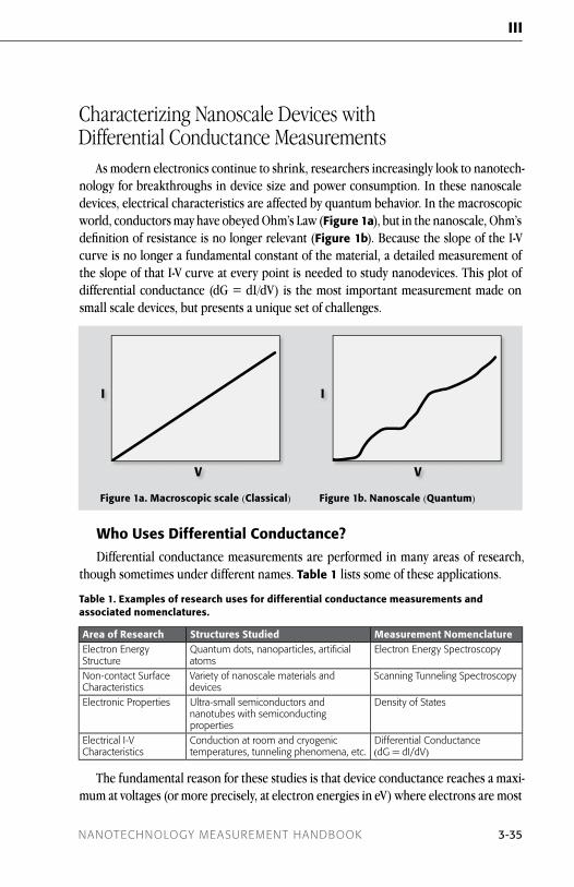
As modern electronics continue to shrink, researchers increasingly look to nanotech-nology for breakthroughs in device size and power consumption. In these nanoscale devices, electrical characteristics are affected by quantum behavior. In the macroscopic world, conductors may have obeyed Ohm’s Law (Figure 1a), but in the nanoscale, Ohm’s definition of resistance is no longer relevant (Figure 1b). Because the slope of the I-V curve is no longer a fundamental constant of the material, a detailed measurement of the slope of that I-V curve at every point is needed to study nanodevices. This plot of differential conductance (dG = dI/dV) is the most important measurement made on small scale devices, but presents a unique set of challenges.
i
V
i
V
Figure 1a. Macroscopic scale (Classical) Figure 1b. nanoscale (Quantum)
Who Uses differential Conductance?
Differential conductance measurements are performed in many areas of research, though sometimes under different names. Table 1 lists some of these applications.
Table 1. examples of research uses for differential conductance measurements and associated nomenclatures.
Area of Research Structures Studied Measurement nomenclatureelectron energy structure
Quantum dots, nanoparticles, artificial atoms
electron energy spectroscopy
non-contact surface characteristics
Variety of nanoscale materials and devices
scanning tunneling spectroscopy
electronic Properties ultra-small semiconductors and nanotubes with semiconducting properties
density of states
electrical i-V characteristics
conduction at room and cryogenic temperatures, tunneling phenomena, etc.
differential conductance (dg = di/dV)
The fundamental reason for these studies is that device conductance reaches a maxi-mum at voltages (or more precisely, at electron energies in eV) where electrons are most

3-36 Keithley instruments, inc .
iii Low-Level Measurement Techniques
active. Thus, dI/dV is directly proportional to the density of states and is the most direct way to measure it.
existing Methods of Measuring differential ConductanceWhile there is no standardized technique for obtaining differential conductance,
almost all approaches follow one of two methods:
(1) Perform a current-voltage sweep (I-V curve) and take the mathematical derivative, or
(2) Superimpose a low amplitude AC sine wave on a stepped DC bias; then use a lock-in amplifier to obtain the AC voltage across the DUT (device under test) and the AC current through it.
I-V Technique
The I-V sweep technique has the advantage of being easier to set up and control. It only requires one source and one measurement in-strument, which makes it relatively easy to co-ordinate and control. The fundamental problem is that even a small amount of noise becomes a large noise when the measurements are differentiated.
Figure 2a shows an I-V curve, which is a series of sourced and measured values (V1, I1), (V2, I2), etc. Several techniques can be used to differentiate this data, but the simplest and most common uses the slope between every pair of consecutive data points. For example, the first point in the differential conductance curve would be (I2–I1)/(V2–V1). Because of the small differences, a small amount of noise in either the voltage or current causes a large un-certainty in the conductance. Figure 2b shows the differentiated curve and the noise, which is unacceptably large for most uses. To reduce this noise, the I-V curve and its derivative can be measured repeatedly. Noise will be reduced by √N, where N is the number of times the curve is measured. After 100 repetitions, which can take
Figure 2a. i-V curve
Figure 2b. differentiated i-V curve
Figure 2c. 100 differentiated curves, averaged together

iii Low-Level Measurement Techniques
nanotechnology measurement handbooK 3-37
iii
more than an hour in a typical application, it is possible to reduce the noise by a factor of 10, as shown in Figure 2c. While this could eventually produce a very clean data set, researchers are forced to accept high noise levels, because measuring 10,000 times to reduce the noise 100× would take far more time than is usually available. Thus, while the I-V curve technique is simple, it forces a trade-off between high noise and very long measurement times.
AC Technique
The AC technique superimposes a low amplitude AC sine wave on a stepped DC bias, as shown in Figure 3. The problem with this method is that, while it provides a mar-ginal improvement in noise over the I-V technique, it imposes a large penalty in terms of system complexity (Figure 4). A typical equipment list includes:
• ACvoltagesourceorfunctiongenerator
• DCbiassource
• SeriesresistororcouplingcapacitortomixACandDCsignals
• Lock-inamplifiersynchronizedtothesourcestofacilitatelow-levelmeasurements
• SeparateinstrumentstomeasureACandDCvoltageandcurrent
Assembling such a system requires extensive time and knowledge of electrical cir-cuitry. Trial and error methods may be required to determine the series resistor and coupling capacitor values based on the unknown DUT impedance and response fre-quency. Long cabling, such as that used in attaching a device in a cryostat, reduces usable frequency and increases noise. In addition, multiple instruments are susceptible to problems of ground loops and common mode current.
Appl
ied
Stim
ulus
Time
Figure 3. The AC technique measures the response to a sine stimulus while sweeping the dC bias through the device’s operating range.
Mixing the AC and DC signals is a significant challenge. It is sometimes done with series resistors and sometimes with blocking capacitors. With either method, the cur-

3-38 Keithley instruments, inc .
iii Low-Level Measurement Techniques
rent through the DUT and the voltage across the DUT are no longer calibrated, so both the AC and DC components of the current and voltage must be measured. A lock-in amplifier may provide the AC stimulus, but frequently the required AC signal is either larger or smaller than a lock-in output can provide, so an external AC source is often required and the lock-in measurements must be synchronized to it.
The choice of frequency for the measurement is another complicating factor. It is desirable to use a frequency that is as high as possible, because a lock-in amplifier’s measurement noise decreases at higher frequencies. However, the DUT’s response fre-quency usually limits the usable frequency to 10–100Hz, where the lock-in amplifier’s measurement noise is five to ten times higher than its best specification. The DUTs response frequency is determined by the device impedance and the cable capacitance, so long cabling, such as that used to attach to a device in a cryostat, reduces the us-able frequency and increases noise, further reducing the intended benefit of the AC technique. Above all, the complexity of the AC method is the biggest drawback, as it requires precise coordination and computer control of six to eight instruments, and it is susceptible to problems of ground loops and common mode current noise.
Another challenge of this method is combining the AC signal and DC bias. There’s no one widely recognized product that addresses this issue. Often, many instruments are massed together in order to meet this requirement. Such instrumentation may include a lock-in amplifier, AC voltage source or function generator (if not using the reference in the lock-in amplifier), DC bias source, DC ammeter, and coupling capacitor/circuitry to combine AC source and DC bias. In many cases, what researchers are really trying to do
dV
dI
DCVoltage
DCVoltmeter
DCMeter
ACVoltage
Lock-In
Lock-In
R1 R2
VDC
IDC
DUT
AC Technique
Figure 4: The AC technique for obtaining differential conductance can use as many as a half dozen components, making it a far more complex setup than the i-V curve method. However, there is a reduction in the amount of noise introduced into the measurement.

iii Low-Level Measurement Techniques
nanotechnology measurement handbooK 3-39
iii
is source current, so the series resistors used to combine the AC and DC must be higher impedance than the device, which is unknown until the measurement is made.
Simple, Low-noise SolutionFortunately, there is a new technique for differential conductance measurements
that is easy to use and provides low-noise results. This improved method uses a four-wire, source current/measure voltage methodology. It requires a precision instrument that combines the DC and AC source components (stimulus), and a nanovoltmeter for the response measurements. These features are contained in the Keithley Models 6220 and 6221 Current Sources and 2182A Nanovoltmeter. The current sources combine the DC and AC components into one source, with no need to do a secondary measure of the current, because its output is much less dependent on the changing device impedance (Figure 5).
dV
dI
DCVoltage
DCVoltmeter
DCMeter
ACVoltage
Lock-In
Lock-In
R1 R2
VDC
IDC
DUT
AC Technique
GPIB orEthernet
RS-232
Trigger Link
DUT
Model 2182A Model 622x
Figure 5. The AC Technique (left) vs. the Keithley Technique (right)
With these instruments, an AC current is superimposed on a linear staircase sweep. The amplitude of the alternating portion of the current is the differential current, dI (Figure 6a). The current source is synchronized with the nanovoltmeter by using a Trigger Link cable. After measuring the voltage at each current step, the nanovoltmeter calculates the delta voltage between consecutive steps. Each delta voltage is averaged with the previous delta voltage to calculate dV. Differential conductance, dG, is then derived from dI/dV (Figure 6b).
Benefits of the Four-Wire, Source i/Measure V MethodThis new method provides low noise results at least 10 times faster than previous
methods. Only two instruments and a single sweep are required. When user-defined currents are small, the performance of instrumentation described above cannot be du-plicated by any user-assembled system in terms of source accuracy, noise, and guarded measurements (the latter being used to reduce DC leakage and improve system response time). AC current can be sourced accurately, even below 10pA. The nanovoltmeter has a sensitivity superior to lock-in amplifiers, low 1/f noise, and automatically compensates

3-40 Keithley instruments, inc .
iii Low-Level Measurement Techniques
for offsets and drift. The four-wire connections eliminate voltage drop errors due to lead or contact resistance, because there is no current flowing through sense leads. This is important when the DUT has regions of low or moderate impedance.
Another key benefit is that more data points can be collected in areas of highest con-ductance (i.e., areas of greatest interest) by sourcing the sweep in equal current steps. Because of the instrumentation’s inherently low source and measurement noise, only one pass is required, shortening data collection time from hours to minutes. Further-more, the instruments’ active guard eliminates the slowing effects of cable capacitance, greatly improving device settling time, measurement speed, and accuracy.
Special CasesSome devices have non-monotonic I-V curves. This behavior is classified as follows:
(1) Current Hop – A given voltage may correlate to more than one possible current.
(2) Negative Differential Conductance (NDC) – A given current may correlate to more than one possible voltage.
With a slight modification, the source current/measure voltage differential conduc-tance method can be used with devices that exhibit these behaviors.
Current Hop
Some devices exhibit an I-V curve where the current is a multi-valued function of voltage (Figure 7a). The negative differential conductance (NDC) region cannot be characterized by applying a voltage source, because any regulated voltage source is unstable into negative resistance loads. Instead, a voltage source would produce a hys-teresis curve that never traces out the NDC region (dashed lines in Figure 7a). Inter-estingly, a current source is not stable over this NDC region either, but adding a series
Appl
ied
Stim
ulus
Time
4th Cycle3rd Cycle
2nd Cycle1st Cycle
MeasV1 Meas
V2
MeasV3 Meas
V4
MeasV5 Meas
V6
2182AV-Meas
622xi-Source
Delay ∆I ∆I
Each A/D conversionintegrates (averages)voltage over a fixed time .
1st Reading ∆V = [(V1–V2) + (V3–V4)]/4
Figure 6a. Applied current during differential conductance sweep.
Figure 6b. detail of applied current and measured voltage.

iii Low-Level Measurement Techniques
nanotechnology measurement handbooK 3-41
iii
resistor in the HI lead presents a composite device to the current source, so that it does not see any NDC region. This resistance must be at least as large as the largest negative resistance throughout the NDC region of the device.
Without any change to the 622x/2182A setup, the entire differential conductance curve can be measured because the four-wire configuration connects the nanovoltme-ter directly across the device and not the series resistor, whose voltage drop is rejected along with all other lead resistance. This lead resistance, which is normally considered a problem, actually makes full characterization possible with these devices. With Keithley’s source-current architecture there is no additional measurement required. Other meth-ods require measurements of both device current and voltage in these cases.
Negative Differential Conductance
If the I-V curve exhibits voltage that is a multi-valued function of current, again, nei-ther voltage nor current sources are stable over the NDC region. To stabilize this meas-urement, it is necessary to add a parallel resistor. The resistance should be low enough
Current
Voltage
Negative differential region:both I and V sourcesunstable, no directmeasurements possible .
Current
Voltage
Series resistoreliminatesNDC region .
Figure 7a. devices with negative differential conductance regions require special treatment.
Figure 7b. The gray curve shows the device voltage as seen by the nanovoltmeter. The pink curve shows the voltage across the device plus the series resistor as seen by current source – no ndC region to create instability.
Current
Voltage
Negative differential region:both I and V sourcesunstable, no directmeasurements possible . Current
Voltage
Resistor in parallelwith DUT eliminatesinstability from NDC .
Figure 8. even when the device shows multiple possible voltages for some currents, differential conductance can easily be obtained with the new method.

3-42 Keithley instruments, inc .
iii Low-Level Measurement Techniques
that the slope of its I-V curve exceeds the maximum slope of the negative resistance region of the device’s I-V curve. That is, the resistance must be smaller than the smallest negative resistance throughout the NDC region of the device. If the chosen resistor is small enough, the slope of the combined I-V response will always be monotonic. The I-V curve traced out is now the sum of both I-V curves (Figure 8b). Because we are measur-ing differential conductance, the conductance of the parallel resistor (1/R) can be simply subtracted from every measurement in the sweep.
ConclusionsWith appropriate instrumentation, the four-wire source current/measure voltage
method is a great improvement over older differential conductance measurements, which are slow, noisy, and complex. The new technique’s single sweep shortens hours of data collection to a few minutes while improving accuracy. Equipment cost is also reduced, since only two instruments are required, instead of six or more.
precision AC/dC Current Source-nanovoltmeter Combo improves Speed and Accuracy of nanotech MeasurementsKeithley’s Model 6221 is an AC and DC Current Source with a Current Source
Waveform Generator. As the only commercially available AC current source, it now eliminates the need for researchers and engineers to build their own instrumenta-tion. By combining the Model 6221 with the Keithley Model 2182A Nanovoltmeter, rapid measurement and characterization of nanoscale devices and materials are easi-ly accomplished. This can be done at very low source currents levels with great preci-sion and without sacrificing accuracy in the lower—and harder to measure—voltages across the sample. Consequently, the Model 6221/2182A combination can measure resistances from 10nΩ to 1GΩ, including delta mode measurements that improve accuracy by up to 1000 times. Used in this way, the Model 6221 acts as a high perfor-mance alternative to AC resistance bridges and lock-in amplifiers, and is especially useful in differential conductance measurements for characterizing semiconductor and nanotechnology devices.
The Model 6221 can be programmed for pulse widths as short as 50 microsec-onds, and supports pulsed I-V measurements. It can source AC currents from 2pA to 100mA and DC currents from 100fA to 100mA with a 10MHz output update rate. The built-in standard and arbitrary waveform generator has a frequency range of 1mHz to 100kHz. The user can define current ramps and program the unit to step through predefined sequences of up to 64,000 output values using a trigger or a timer. Linear, logarithmic, and custom sweeps are supported. Programming can be done from the front panel controls or from an external controller via an RS-232, GPIB, or Ethernet interface. Included control software simplifies setup and operation.
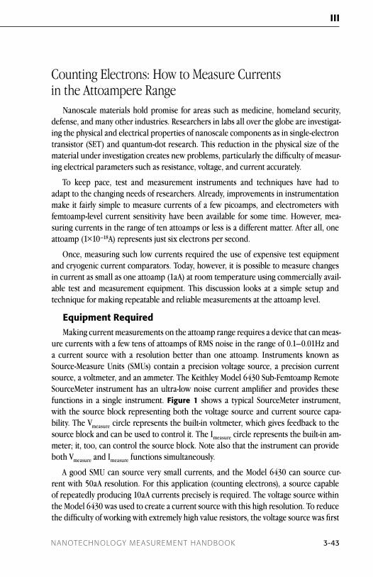
iii Low-Level Measurement Techniques
nanotechnology measurement handbooK 3-43
iii
Counting Electrons: How to Measure Currents in the Attoampere Range
Nanoscale materials hold promise for areas such as medicine, homeland security, defense, and many other industries. Researchers in labs all over the globe are investigat-ing the physical and electrical properties of nanoscale components as in single-electron transistor (SET) and quantum-dot research. This reduction in the physical size of the material under investigation creates new problems, particularly the difficulty of measur-ing electrical parameters such as resistance, voltage, and current accurately.
To keep pace, test and measurement instruments and techniques have had to adapt to the changing needs of researchers. Already, improvements in instrumentation make it fairly simple to measure currents of a few picoamps, and electrometers with femtoamp-level current sensitivity have been available for some time. However, mea-suring currents in the range of ten attoamps or less is a different matter. After all, one attoamp (1×10–18A) represents just six electrons per second.
Once, measuring such low currents required the use of expensive test equipment and cryogenic current comparators. Today, however, it is possible to measure changes in current as small as one attoamp (1aA) at room temperature using commercially avail-able test and measurement equipment. This discussion looks at a simple setup and technique for making repeatable and reliable measurements at the attoamp level.
equipment Required
Making current measurements on the attoamp range requires a device that can meas-ure currents with a few tens of attoamps of RMS noise in the range of 0.1–0.01Hz and a current source with a resolution better than one attoamp. Instruments known as Source-Measure Units (SMUs) contain a precision voltage source, a precision current source, a voltmeter, and an ammeter. The Keithley Model 6430 Sub-Femtoamp Remote SourceMeter instrument has an ultra-low noise current amplifier and provides these functions in a single instrument. Figure 1 shows a typical SourceMeter instrument, with the source block representing both the voltage source and current source capa-bility. The Vmeasure circle represents the built-in voltmeter, which gives feedback to the source block and can be used to control it. The Imeasure circle represents the built-in am-meter; it, too, can control the source block. Note also that the instrument can provide both Vmeasure and Imeasure functions simultaneously.
A good SMU can source very small currents, and the Model 6430 can source cur-rent with 50aA resolution. For this application (counting electrons), a source capable of repeatedly producing 10aA currents precisely is required. The voltage source within the Model 6430 was used to create a current source with this high resolution. To reduce the difficulty of working with extremely high value resistors, the voltage source was first
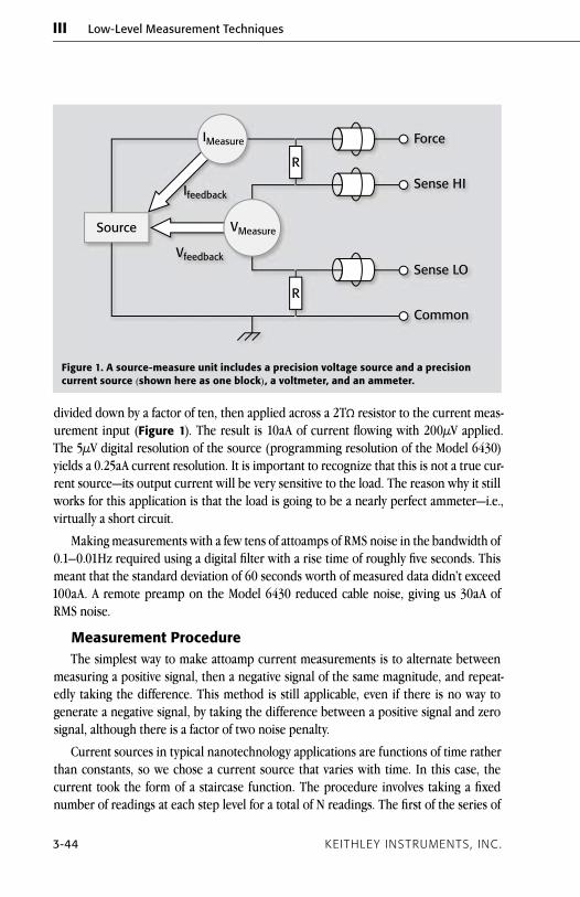
3-44 Keithley instruments, inc .
iii Low-Level Measurement Techniques
divided down by a factor of ten, then applied across a 2TΩ resistor to the current meas-urement input (Figure 1). The result is 10aA of current flowing with 200µV applied. The 5µV digital resolution of the source (programming resolution of the Model 6430) yields a 0.25aA current resolution. It is important to recognize that this is not a true cur-rent source—its output current will be very sensitive to the load. The reason why it still works for this application is that the load is going to be a nearly perfect ammeter—i.e., virtually a short circuit.
Making measurements with a few tens of attoamps of RMS noise in the bandwidth of 0.1–0.01Hz required using a digital filter with a rise time of roughly five seconds. This meant that the standard deviation of 60 seconds worth of measured data didn’t exceed 100aA. A remote preamp on the Model 6430 reduced cable noise, giving us 30aA of RMS noise.
Measurement procedureThe simplest way to make attoamp current measurements is to alternate between
measuring a positive signal, then a negative signal of the same magnitude, and repeat-edly taking the difference. This method is still applicable, even if there is no way to generate a negative signal, by taking the difference between a positive signal and zero signal, although there is a factor of two noise penalty.
Current sources in typical nanotechnology applications are functions of time rather than constants, so we chose a current source that varies with time. In this case, the current took the form of a staircase function. The procedure involves taking a fixed number of readings at each step level for a total of N readings. The first of the series of
Source
IMeasure
VMeasure
Ifeedback
Vfeedback
R
R
Force
Sense HI
Sense LO
Common
Figure 1. A source-measure unit includes a precision voltage source and a precision current source (shown here as one block), a voltmeter, and an ammeter.
iii Low-Level Measurement Techniques
nanotechnology measurement handbooK 3-45
iii
readings taken with the positive source applied is averaged with the negative of the first in the series of readings taken with the negative source applied. In equation form, this is expressed as:
(In+ – In
–) In = _________ 2
The division by two comes about because the signal-to-noise ratio is the same in both signals, but there is twice the signal present in the full plus-to-minus signal. For signals with no negative component, the equation is identical except there is no division by two. Doing this for each of the readings in the series yields a series of difference read-ings. The whole process is repeated several times and averaged. Each difference series is averaged point-by-point, resulting in a single series of readings representing the current shape produced by the source.
Setting Up the MeasurementChoosing how fast to alternate between positive and negative sourcing requires
some balancing. Faster alternations help minimize the effects of slow drifts in input current and also reduce noise. But, with teraohms of resistance in the source (which is typical for any source generating such small currents), the settling time is one to two seconds. If the source alternated every few seconds, most of the measurement would be of the source settling rather than the final DC value. One way to solve this is to let the source settle for ten percent of the time after each alternation and measure for 90 percent of the time—which means a half-period of ten times the settling time, or about 20 seconds.
Using this mathematical technique, the valid points from the current shape (i.e., the last 90 percent) were averaged to produce the final measurement. Estimating the error in this mean value required using the statistics of uncorrelated noise. Instead of one final current shape averaged from many difference series, N current shapes were generated. Each of these current shapes yields a mean from its valid data points so the collection of mean values has a standard deviation. Because the means are uncorrelated, the final answer, the mean of the N means, has a one sigma uncertainty equal to the standard deviation of the collection of means divided by the square root of N.
2TΩR
9R
I
SMU
GuardBuffer
Figure 2. The schematic shows a basic measurement circuit.
3-46 Keithley instruments, inc .
iii Low-Level Measurement Techniques
This was verified by generating 1,000 current shapes and plotting the standard devia-tions of the collections for N = 1000, 500, 250, etc. As expected, the standard deviations of the collections dropped as the square root of the number of means in the collection.
Results
For the simplest case, using a single current value and using 40 seconds for each source polarity, after one hour of measurement or 45 reversal pairs, the uncertainty was about 2.6 attoamps. After 12 hours of averaging, the uncertainty fell to about 0.75 attoamps. After several such 12-hour runs, the collection of results had a standard devia-tion consistent with 0.75 attoamps.
A good way to estimate the time required to achieve these results on an arbitrary system with unknown external noise sources is to measure the noise of the system in the 0.1–0.01Hz bandwidth as described earlier. The test system, with the source on but constant, measured 60aA RMS in this bandwidth. If another system had 120aA, it is reasonable to expect that each of the uncertainties achieved here could be done in approximately four times the amount of time.
physical precautions
The largest contributor to low-frequency noise in this sort of test setup is tempera-ture variation. Instrument offset currents vary with ambient temperature, in this case by less than 500aA/°C. But even slow temperature changes from a building’s heating and cooling systems could cause large current changes. One way of avoiding this problem is to simply place a cardboard box over the low current amplifier and source fixture. Doing so nearly eliminates the problem. It is critically important that the low current amplifier have low power dissipation (in this case <1/3 watt) to avoid heat buildup in the enclosure.
Another concern is stray electrostatic fields. Housing the current-generating element (in this case the source’s resistors) in an electrostatic shield that is grounded for safety eliminates this problem. It’s also possible to improve the settling time of the source by placing the current-generating element inside an inner electrostatic shield driven by the guard buffer.
Time-Varying input
Using a slow staircase input instead of a simple DC signal shows that a discernable signal can be retrieved from the noise. After every 90 measurements (about 18 sec-onds), the current source was incremented by 10aA. Inverting the staircase generated the negative source period. The results are shown in Figure 3.

iii Low-Level Measurement Techniques
nanotechnology measurement handbooK 3-47
iii
Considering each step as a separate measurement and using the estimates described earlier, the mean of each current step has a one-sigma uncertainty of 0.8 attoamps (Figure 4). The measurement took 84 hours, only slightly longer than the equivalent of five 12-hour runs for five separate measurements. The extra time required to reduce the noise is expected. The longer alternation period allows offsets to drift more be-tween the positive and negative measurements, so the residual noise is larger. This can also be described by noting that offset drift due to temperature change typically has a 1/f characteristic. That is, noise current is inversely proportional to frequency (Figure
5). So, while the current reversal process still narrows the bandwidth to 1/(12 hours)
10
1s o
f co
llect
ion
of a
vera
ges
n, number of samples averaged
noise reduction 1/ n as n increases: Best fit is n -.5015
100 1000
1E–16
1E–17
1E–18
1E–19
Figure 3. The graph depicts a plot estimating the uncertainty in the mean, which is ±0.8aA.
50
40
30
20
10
0
–10
–20
–30
–40
–50
Seconds
Attoamps
0 50 100 150 200 250
Figure 4. A graph of the staircase current waveform used in the experimental setup.

3-48 Keithley instruments, inc .
iii Low-Level Measurement Techniques
(0.00002Hz), the lower alternation frequency of the staircase places the measurement higher on the 1/f curve.
ConclusionsUsing the data analyses and filtering described here, a wide range of tradeoffs be-
tween measurement time and uncertainty can be obtained. In addition, if proper at-tention is given to relevant noise sources such as temperature and cabling, current measurements can be made well below the one femtoamp level. In fact, using commer-cially available test equipment, measurements with uncertainties of one attoampere and below are possible and indeed practical.
1E–13
1E–14
1E–15
1E–16
1E–171E–6 1E–5 1E–4 1E–3 1E–2 1E–1 1E+0 1E+1
Frequency
6430 Spectral noise distribution
Instrument aloneWith experimental apparatus
Figure 5. The noise spectrum of the experimental setup shows that noise decreases with increasing frequency.

iii Low-Level Measurement Techniques
nanotechnology measurement handbooK 3-49
iii
A Feel for the PulseUnderstanding your test requirements will help you select the right pulse generator for the job.
Rapidly changing and advancing technology continually challenges test equipment manufacturers to develop new systems for testing the latest generation of electronic de-vices and materials. Industries such as semiconductor and communication technology, with rapid development of new standards, often require cutting-edge device testing and new source and measurement capabilities.
In recent years, new testing techniques have been developed to meet these challeng-es. One such technique is pulse testing. The uses for instruments with pulse capabilities are many, for instance, testing advanced semiconductor devices as well as RF devices such as high-speed serial communications links.
pulse Testing
Pulse testing involves delivering a single pulse to an output. This pulse is used to test a variety of things, such as for transient testing of a device to determine its transfer function and thereby characterize the material under test.
Pulse or pattern generators (Figure 1) are used in a wide variety of applications in both the lab and on the production line. Researchers often need to stimulate a device under test (DUT) with a pulse, series of pulses (Figure 2a), or known data patterns at specified rates in order to characterize device performance. Pulse or pattern generators are often configured into test systems that also include SMUs, digital multimeters, volt-meters, switches, and oscilloscopes (Figure 2b).
Figure 1. Keithley’s Series 3400 pulse/pattern Generators feature a frequency range from 1mHz to 165MHz with programmable rise and fall times down to two nanoseconds.

3-50 Keithley instruments, inc .
iii Low-Level Measurement Techniques
An example of an application where a pulse/pattern generator is an important tool is in the testing of program/erase cycles in memory devices (Figure 3). Two of the tests performed for this type of application are endurance and speed tests. For these types of test, a pulse should be applied at one polarity to write to the device, and a pulse should be applied at the opposite polarity with a larger amplitude to erase memory. For endur-ance tests, program/erase actions must be cycled as quickly as possible while perform-ing DC threshold (Vt) tests on the transistors. For speed tests, the pulse width and/or amplitude are varied until the optimal threshold voltages for the program and erase functions are found. During this test, a DC Vt test must be performed on the transistors between every program or erase pulse.
need for pulse Testing
The need for pulse sources has been growing over time. Shrinking device geometries, new materials, and more complex designs are having a tremendous impact on device lifetimes due to increased fragility, higher power density, and new failure mechanisms. This need is driven in part by the higher operating speeds of today’s electronic circuits. The higher operating speed requires test equipment that can produce simulated clock and data signals at the rate that the circuit will actually perform (Figure 4).
Also, analog components used in these circuits behave differently at higher speeds, so they can’t be characterized at DC using traditional DC methods. Because pulse sizes can be made extremely small, on the order of a few nanoseconds, pulse testing over-comes the problems inherent in DC testing techniques. Therefore, pulsed test signals are needed to characterize these components.
In addition, as components have become smaller, the need for pulsed testing tech-niques becomes more critical. Smaller DUTs are more susceptible to self-heating, which can destroy or damage the part or change its response to test signals, masking the
Figure 2a. example of a pulse/pattern output
Figure 2b. Measured response from a device using pulse testing

iii Low-Level Measurement Techniques
nanotechnology measurement handbooK 3-51
iii
Figure 3. example application: program/erase cycles on memory devices.
Figure 4. pulse/pattern generators must provide simulated clock and data signals at the rate the circuit will actually perform.
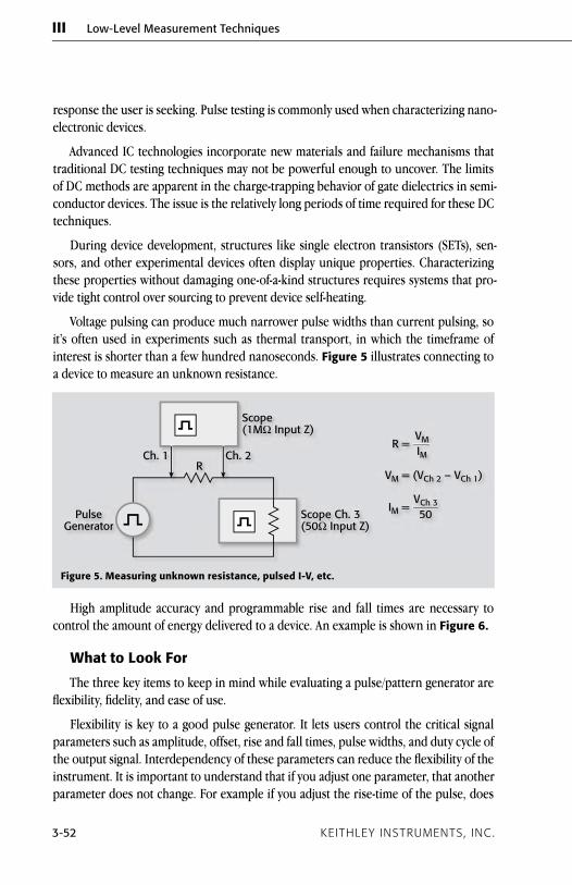
3-52 Keithley instruments, inc .
iii Low-Level Measurement Techniques
response the user is seeking. Pulse testing is commonly used when characterizing nano-electronic devices.
Advanced IC technologies incorporate new materials and failure mechanisms that traditional DC testing techniques may not be powerful enough to uncover. The limits of DC methods are apparent in the charge-trapping behavior of gate dielectrics in semi-conductor devices. The issue is the relatively long periods of time required for these DC techniques.
During device development, structures like single electron transistors (SETs), sen-sors, and other experimental devices often display unique properties. Characterizing these properties without damaging one-of-a-kind structures requires systems that pro-vide tight control over sourcing to prevent device self-heating.
Voltage pulsing can produce much narrower pulse widths than current pulsing, so it’s often used in experiments such as thermal transport, in which the timeframe of interest is shorter than a few hundred nanoseconds. Figure 5 illustrates connecting to a device to measure an unknown resistance.
Scope(1MΩ Input Z)
Ch . 2Ch . 1R
PulseGenerator
Scope Ch . 3(50Ω Input Z)
R =VMIM
VM = (VCh 2 – VCh 1)
IM =VCh 350
Figure 5. Measuring unknown resistance, pulsed i-V, etc.
High amplitude accuracy and programmable rise and fall times are necessary to control the amount of energy delivered to a device. An example is shown in Figure 6.
What to Look For
The three key items to keep in mind while evaluating a pulse/pattern generator are flexibility, fidelity, and ease of use.
Flexibility is key to a good pulse generator. It lets users control the critical signal parameters such as amplitude, offset, rise and fall times, pulse widths, and duty cycle of the output signal. Interdependency of these parameters can reduce the flexibility of the instrument. It is important to understand that if you adjust one parameter, that another parameter does not change. For example if you adjust the rise-time of the pulse, does
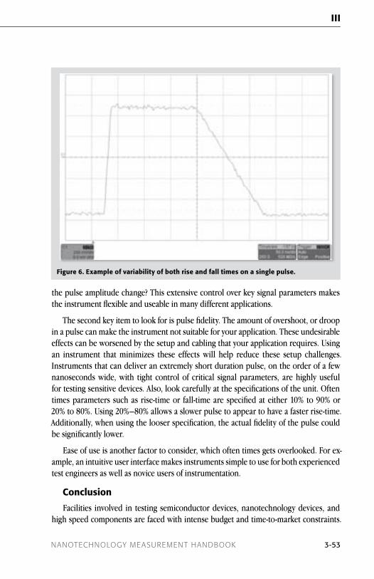
iii Low-Level Measurement Techniques
nanotechnology measurement handbooK 3-53
iii
the pulse amplitude change? This extensive control over key signal parameters makes the instrument flexible and useable in many different applications.
The second key item to look for is pulse fidelity. The amount of overshoot, or droop in a pulse can make the instrument not suitable for your application. These undesirable effects can be worsened by the setup and cabling that your application requires. Using an instrument that minimizes these effects will help reduce these setup challenges. Instruments that can deliver an extremely short duration pulse, on the order of a few nanoseconds wide, with tight control of critical signal parameters, are highly useful for testing sensitive devices. Also, look carefully at the specifications of the unit. Often times parameters such as rise-time or fall-time are specified at either 10% to 90% or 20% to 80%. Using 20%–80% allows a slower pulse to appear to have a faster rise-time. Additionally, when using the looser specification, the actual fidelity of the pulse could be significantly lower.
Ease of use is another factor to consider, which often times gets overlooked. For ex-ample, an intuitive user interface makes instruments simple to use for both experienced test engineers as well as novice users of instrumentation.
Conclusion
Facilities involved in testing semiconductor devices, nanotechnology devices, and high speed components are faced with intense budget and time-to-market constraints.
Figure 6. example of variability of both rise and fall times on a single pulse.

3-54 Keithley instruments, inc .
iii Low-Level Measurement Techniques
However, they cannot compromise on measurement quality, valuable rack or bench-top space, or ease of use. These designers have a need for test instruments such as pulse generators that satisfy their needs for current as well as future testing.
dC Source
dC Source
dual-Channeldigital
oscilloscope forMeasurement
dual-Channelpulse Generator
Trigger
AC+dCout
AC+dCout
dC
dC
Figure 7. The 4200-piV option bundle for the Model 4200-SCS includes everything needed to implement a turnkey system for pulsed i-V testing of leading-edge devices and materials:
• Integrateddual-channelpulsegeneratorandGUIforstand-alonecontrolasdesired
• Dual-channelhighspeedpulsemeasurement
• PIVcontrolsoftware(patent pending)
• InterconnectfixturedesignedtominimizethesignalreflectionscommontopulseI-Vtesting (patent pending)
• Allrequiredconnectorsandcables
• PulseI-VsampleprojectcreatedforisothermaltestingofFinFETs,SOIdevices,powerdevices, and Laterally diffused Metal oxide Semiconductors (LdMoSs)
• Charge-trappingsampleprojectcreatedforhighk gate stack characterization

iii Low-Level Measurement Techniques
n a n o t e c h n o l o g y m e a s u r e m e n t h a n d b o o K
S e C T i o n i V
Nanomaterials Research
4-2 Keithley instruments, inc .
iV Nanomaterials Research
Electronic Transport Characteristics of Gallium Nitride Nanowire-based Nanocircuits
Electronic transport studies of a two-phase gallium nitride nanowire were explored. The steps taken are briefly described here and discussed in detail below.
Current-voltage measurements were taken of gallium nitride based three terminal field effect transistors fabricated via electron beam lithography. The measurements in-dicated a working field effect transistor using a global back gate configuration. Very high current levels within the nanowire were reported. Direct transport measurements were also taken via two nanomanipulator probes. High current levels in this experi-ment were also observed. Scanning Probe Re cog ni tion Mi cro scopy was used to detect the contact pad and nanowire radial boundary, and a nanowire auto- fo cus ex per i ment was reported.
introduction
Over the past decade nanowires and nanotubes made from a wide variety of materi-als have demonstrated extraordinary electronic, mechanical, and chemical characteris-tics. Gallium nitride (GaN) nanowires are particularly promising due to an inherently wide bandgap coupled with structurally induced electronic and optical confinement [1]. Gallium nitride-based nanocircuits have recently been shown to be viable for wide range of electronic and optical applications. GaN nanowire field effect transistors [2, 3, 4] and logic devices [5] have shown the desired characteristics of high transconduc-tance and good switching, and room temperature UV lasing has been reported for GaN nanowire systems [6, 7] as well as good field emission properties [8].
Understanding the interactions of gallium nitride nanowires within a nanocircuit architecture is critically important to the maximizing the potential of the GaN nanowire building block. In particular, details of the electronic transport and carrier injection require fundamental elucidation. This discussion will present details of an investigation into electronic transport and carrier injection.
Materials and Methods
The ~50–100nm gallium nitride nanowires were grown in a direct reaction of metal gallium vapor with flowing ammonia at 850–900°C without a catalyst, as reported in Reference [9]. These had a two-phase coaxial zinc-blende/wurtzite structure, shown in Figure 1 and reported in Reference [10]. A field effect transistor design using a GaN nanowire as an n-type semiconducting channel was used in the experiment (GaNFET). The nanowires were dispersed on a highly doped p-type silicon substrate covered with a 150nm dielectric layer of thermally grown silicon dioxide. The GaNFET source and drain contacts were patterned using electron beam lithography, with Ti/Au used for the
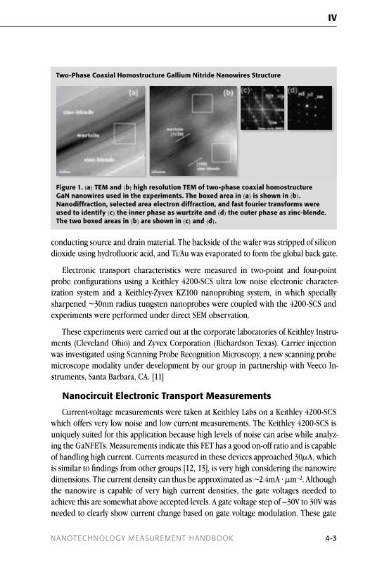
iV Nanomaterials Research
nanotechnology measurement handbooK 4-3
iV
conducting source and drain material. The backside of the wafer was stripped of silicon dioxide using hydrofluoric acid, and Ti/Au was evaporated to form the global back gate.
Electronic transport characteristics were measured in two-point and four-point probe configurations using a Keithley 4200-SCS ultra low noise electronic character-ization system and a Keithley-Zyvex KZ100 nanoprobing system, in which specially sharpened ~30nm radius tungsten nanoprobes were coupled with the 4200-SCS and experiments were performed under direct SEM observation.
These experiments were carried out at the corporate laboratories of Keithley Instru-ments (Cleveland Ohio) and Zyvex Corporation (Richardson Texas). Carrier injection was investigated using Scanning Probe Recognition Microscopy, a new scanning probe microscope modality under development by our group in partnership with Veeco In-struments, Santa Barbara, CA. [11]
nanocircuit electronic Transport Measurements
Current-voltage measurements were taken at Keithley Labs on a Keithley 4200-SCS which offers very low noise and low current measurements. The Keithley 4200-SCS is uniquely suited for this application because high levels of noise can arise while analyz-ing the GaNFETs. Measurements indicate this FET has a good on-off ratio and is capable of handling high current. Currents measured in these devices approached 30µA, which is similar to findings from other groups [12, 13], is very high considering the nanowire dimensions. The current density can thus be approximated as ~2.4mA · µm–2. Although the nanowire is capable of very high current densities, the gate voltages needed to achieve this are somewhat above accepted levels. A gate voltage step of –30V to 30V was needed to clearly show current change based on gate voltage modulation. These gate
Two-phase Coaxial Homostructure Gallium nitride nanowires Structure
Figure 1. (a) TeM and (b) high resolution TeM of two-phase coaxial homostructure Gan nanowires used in the experiments. The boxed area in (a) is shown in (b). nanodiffraction, selected area electron diffraction, and fast fourier transforms were used to identify (c) the inner phase as wurtzite and (d) the outer phase as zinc-blende. The two boxed areas in (b) are shown in (c) and (d).
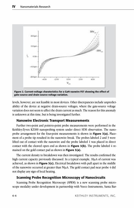
4-4 Keithley instruments, inc .
iV Nanomaterials Research
levels, however, are not feasible in most devices. Other discrepancies include unpredict-ability of the device at negative drain-source voltages, where the gate-source voltage variation does not seem to affect the drain current as much. The reason for this anomaly is unknown at this time, but is being investigated further.
nanowire electronic Transport MeasurementsFurther two-point and point-to-point probe measurements were performed in the
Keithley-Zyvex KZ100 nanoprobing system under direct SEM observation. The nano-probe arrangement for the four-point measurements is shown in Figure 3(a). Place-ment of a probe tip resulted in the nanowire break. The probes labeled 2 and 3 were lifted out of contact with the nanowire and the probe labeled 1 was placed in direct contact with the cleaved open end as shown in Figure 3(b). The probe labeled 4 re-mained on the gold contact pad as shown in Figure 3(a).
The current density to breakdown was then investigated. The results confirmed the high current capacity previously discussed. In a typical example, 10µA of current was achieved, as shown in Figure 3(c). Electrical breakdown with pull apart in the middle of the nanowire occurred at greater than 50µA. The gold contact pad near probe 4 did not display any sign of local heating.
Scanning probe Recognition Microscopy of nanocircuitsScanning Probe Recognition Microscopy (SPRM) is a new scanning probe micro-
scope modality under development in partnership with Veeco Instruments, Santa Bar-
Figure 2. Current-voltage charateristics for a Gan naowire FeT showing the effect of gate-source and drain-source voltage variation.

iV Nanomaterials Research
nanotechnology measurement handbooK 4-5
iV
bara, California [14]. In SPRM, we give the Scanning Probe Microscope (SPM) system itself the power to return to a specific nanoscale feature of interest through feature recognition coupled with adaptive scan plan generation and implementation. It is a recognition-driven and learning approach, made possible through combining Scan-ning Probe Micro scope piezoelectric implementation with on-line image processing and dynam ically adaptive learning algorithms. The human operator interaction is now focused on the decision-making level, rather than the execution level.
SPRM has been implemented in the main atomic force and scanning tunneling modes. The SPRM experiments are performed on a specially adapted Multimode Nano-scope IIIA (Veeco Instruments) in ambient air. For the nanociruits investigation, several aspects of the GaNFETs are currently under investigation, which require the ability to auto-focus the scan path to proceeed from the conducting contact pad onto the semi-conducting GaN nanowire, while avoiding the insulating oxide layer.
Our implementation, shown in Figure 4, uses real-time captured information to detect the contact pad (user defined region), the contact pad-nanowire linear junction, and the nanowire radial boundary. Our current implementation also has an adaptive learning capability with statistical methods that can be used in boundary detection adjustment to improve accuracy.
The resulting nanowire auto-focus using SPRM is shown in Figure 4. The image cap-tured by the SPM is shown in Figure 4 (a) (dotted lines are used to artificially enhance
Figure 3. (a) nanoprobe arrangement for the four-point measurements. (b) probe 1 placed in direct contact with the cleaved nanowire open end. (c) example high current density i-V char ac ter ist ic.
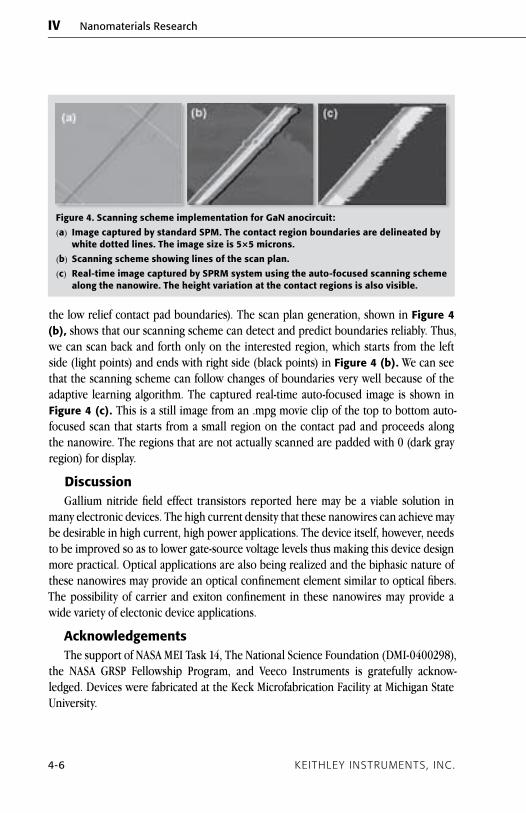
4-6 Keithley instruments, inc .
iV Nanomaterials Research
the low relief contact pad boundaries). The scan plan generation, shown in Figure 4 (b), shows that our scanning scheme can detect and predict boundaries reliably. Thus, we can scan back and forth only on the interested region, which starts from the left side (light points) and ends with right side (black points) in Figure 4 (b). We can see that the scanning scheme can follow changes of boundaries very well because of the adaptive learning algorithm. The captured real-time auto-focused image is shown in Figure 4 (c). This is a still image from an .mpg movie clip of the top to bottom auto-focused scan that starts from a small region on the contact pad and proceeds along the nanowire. The regions that are not actually scanned are padded with 0 (dark gray region) for display.
discussionGallium nitride field effect transistors reported here may be a viable solution in
many electronic devices. The high current density that these nanowires can achieve may be desirable in high current, high power applications. The device itself, however, needs to be improved so as to lower gate-source voltage levels thus making this device design more practical. Optical applications are also being realized and the biphasic nature of these nanowires may provide an optical confinement element similar to optical fibers. The possibility of carrier and exiton confinement in these nanowires may provide a wide variety of electonic device applications.
AcknowledgementsThe support of NASA MEI Task 14, The National Science Foundation (DMI-0400298),
the NASA GRSP Fellowship Program, and Veeco Instruments is gratefully acknow-ledged. Devices were fabricated at the Keck Microfabrication Facility at Michigan State University.
Figure 4. Scanning scheme implementation for Gan anocircuit:
(a) image captured by standard SpM. The contact region boundaries are delineated by white dotted lines. The image size is 5×5 microns.
(b) Scanning scheme showing lines of the scan plan.
(c) Real-time image captured by SpRM system using the auto-focused scanning scheme along the nanowire. The height variation at the contact regions is also visible.

iV Nanomaterials Research
nanotechnology measurement handbooK 4-7
iV
References[1] J. C. Johnson, H-J Choi, K. P. Knutsen, R. D. Schaller, P. Yang, R. J. Saykally, “Single gallium
nitride nanowire lasers,” Nat. Mater. Lett., 1, R106 (2002).
[2] Y. Huang, X. Duan, Y. Cui, C. M. Lieber, “Gallium nitride nanowire nanodevices,” Nano Lett., 2, R101 (2002).
[3] E. Stern, G. Cheng, E. Cimpoiasu, R. Klie, S. Guthrie, J. Klemic, I. Kretzschmar, E. Steinlauf, D. Turner-Evans, E. Broomfield, J. Hyland, R. Koudelka, T. Boone, M. Young, A. Sanders, R. Munden, T. Lee, D. Routenberg, M. A. Reed, “Electrical characterization of single GaN nanowires,” Nanotechnology, 16, R2941 (2005).
[4] J. M. Barker, K. A. Bertness, N. A. Sanford, “Electrical measurements of GaN nanowires deposited using electric-field assisted alignment,” 6th International Conference on Nitride Semiconductors, Tu-P-123.
[5] Y. Huang, X. Duan, Y. Cui, L. J. Lauhon, K. H. Kim, C. M. Lieber, “Logic gates and computa-tion from assembled nanowire building blocks,” Science, 294, R1313 (2001).
[6] F. Qian, S. Gradecak, Y. Li, C. Wen and C.M. Lieber, “Core/multishell nanowire heterostruc-tures as multicolor, high-efficiency light-emitting diodes,” Nano Lett., 5, R2287, (2005).
[7] S. Gradecak, F. Qian, Y. Li, H.-G. Park and C.M. Lieber, “GaN nanowire lasers with low lasing thresholds,” Appl. Phys. Lett., 87, R173111, (2005).
[8] C-C. Chen, C-C. Yeh, C-H. Chen, M-Y. Yu, H-L. Liu, J-J. Wu, K-H. Chen, L-C. Chen, J-Y. Peng, Y-F. Chen, “Catalytic growth and characterization of gallium nitride nanowires,” J. Am. Chem. Soc., 123, R2791 (2001).
[9] M. He, P. Zhou, S. N. Mohammad, G. L. Harris, J. B. Halpern, R. Jacobs, W. L. Sarney, L. Sala-manca-Riba, “Growth of GaN nanowires by direct reaction of Ga with NH3,” J. of Crys. Grow., 231, 357 (2001).
[10] V.M. Ayres, B.W. Jacobs, M.E. Englund, E.H. Carey, M.A. Crimp, R.M. Ronningen, A.F. Zeller, J.B. Halpern, M.-Q. He, G.L. Harris, D. Liu, H.C. Shaw and M.P. Petkov, “Investigation of heavy ion irradiation of gallium nitride nanowires and nanocircuits,” in press, Diamond and Related Materials, (2006).
[11] http://www .nsf .gov/awardsearch/showAward .do?AwardNumber=0400298
[12] H-Y. Cha, H. Wu, M. Chandrashekhar, Y. C. Choi1, S. Chae, G. Koley, M. G. Spencer, “Fabrica-tion and characterization of pre-aligned gallium nitride nanowire field-effect transistors,” Nanotechnology, 17, R1264 (2006).
[13] C. Y. Nam, J. Y. Kim, J. E. Fischer, “Focused-ion-beam platinum nanopatterning for GaN nanowires: ohmic contacts and patterned growth,” Nano Lett., 5, R2029 (2005).
[14] http://www .nsf .gov/awardsearch/showAward .do?AwardNumber=0400298
Keithley gratefully acknowledges the assistance of Dr. V. M. Ayres of Michigan State University, who granted permission to reprint this paper. It received the “Best Student Poster” award at IEEE Nano2006, held July 17–20, 2006, in Cincinnati, Ohio.

4-8 Keithley instruments, inc .
iV Nanomaterials Research
iV Nanomaterials Research
n a n o t e c h n o l o g y m e a s u r e m e n t h a n d b o o K
S e C T i o n V
Nanodevice Measurement Techniques

5-2 Keithley instruments, inc .
V Nanodevice Measurement Techniques
Tips for Electrical Characterization of Carbon Nanotubes and Low Power Nanoscale Devices
The potential uses for carbon nanotubes are seemingly endless, with plenty of poten-tial applications in the semiconductor industry alone. Researchers are already incorpo-rating carbon nanotubes into FETs for switches, memory for consumer goods, and field emission displays for the next generation of televisions. Researchers are also looking into applying carbon nanotubes in sensor applications to detect molecular particles for applications in homeland security. There is also serious work being done to use carbon nanotubes transistors for digital logic.
The semiconductor and nanotechnology communities continue to be faced with challenges when working with carbon nanotubes and other low power nanoscale de-vices. One challenge is the difficulty of electrically characterizing extremely small circuit elements, not only in the current generation of semiconductors, but in next-generation nanoscale electronics as well.
A second challenge is how to characterize these next generation devices when power limitation is critical. The scaling of devices and components to the nano scale forces re-searchers to limit the levels of electrical signals that can be applied for characterization.
Lastly, probing nanoscale devices continues to be a challenge. With standard gate dimensions of less than 90nm and space budgets shrinking continuously, the small-est probe pad dimensions required for most prober systems remain fixed at about 50 microns. This limitation is largely the result of the inaccuracy of probe movements and the size of the probe tips. This challenge is being solved with new probing tools that offer nanometer movement precision with probe tip diameters of less than 50nm and current measuring capability better than 1pA (see Figure 1).
This discussion focuses on measurement techniques that can be applied to char-acterizing carbon nanotubes low power devices, and what can be done to overcome various sources of measurement error.
Methods and TechniquesConsumers are demanding faster, more feature-rich products in ever-smaller form
factors. Because the electronics must have smaller sizes, the components will also have limited power handling capability. As a result, when electrically characterizing these components, the test signals need to be kept small to prevent component breakdown or other damage. Current versus Voltage (I-V) characterization on nanoscale devices may require the measurement of very small voltages due to the necessity of applying a very small current to control power or to reduce the Joule-heating effects. Therefore, low level voltage measurement techniques become important, not only for I-V charac-terization of devices but also for resistance measurements of non-conductive materials

V Nanodevice Measurement Techniques
nanotechnology measurement handbooK 5-3
V
and components. For researchers and electronics industry test engineers, this power limitation makes characterizing modern devices and materials and future devices challenging.
Unlike I-V curve generation on macro- and micro-scale components and materials, measurements on carbon nanotubes and nanoscale devices require such special care and techniques. General-purpose I-V curve characterizations are often performed using a two-point electrical measurement technique. The problem with this method is that the voltage is measured not only across the device in question, but includes the voltage drop across the test leads and contacts as well. If your goal is to measure the resistance
Ai (
Am
ps)
AV (Volts)
3 .00E–07
2 .00E–07
1 .00E–07
0 .00E–07
–1 .00E–07
–2 .00E–07
–3 .00E–07
–0 .5 –0 .4 –0 .3 –0 .2 –0 .1 0 .0 0 .1 0 .2 0 .3 0 .4 0 .5
Figure 1. i-V curve on a carbon nanotube.
Figure 1a. Keithley’s Model 4200-SCS semiconductor characterization system.
Figure 1b. Zyvex S100 nanomanipulator.
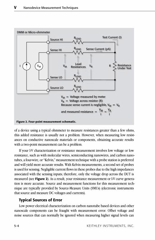
5-4 Keithley instruments, inc .
V Nanodevice Measurement Techniques
of a device using a typical ohmmeter to measure resistances greater than a few ohms, this added resistance is usually not a problem. However, when measuring low resist-ances on conductive nanoscale materials or components, obtaining accurate results with a two-point measurement can be a problem.
If your I-V characterization or resistance measurement involves low voltage or low resistance, such as with molecular wires, semiconducting nanowires, and carbon nano-tubes, a four-wire, or “Kelvin,” measurement technique with a probe station is preferred and will yield more accurate results. With Kelvin measurements, a second set of probes is used for sensing. Negligible current flows in these probes due to the high impedances associated with the sensing inputs; therefore, only the voltage drop across the DUT is measured (see Figure 2). As a result, your resistance measurement or I-V curve genera-tion is more accurate. Source and measurement functions for this measurement tech-nique are typically provided by Source-Measure Units (SMUs) (electronic instruments that source and measure DC voltages and currents).
Typical Sources of errorLow power electrical characterization on carbon nanotube based devices and other
nanoscale components can be fraught with measurement error. Offset voltage and noise sources that can normally be ignored when measuring higher signal levels can
Test Current (I)
RLEAD
I VM
Sense HI
Sense LO
VM
RLEAD
VR R ResistanceUnder Test
LeadResistances
DMM or Micro-ohmmeter
VM = Voltage measured by meterVR = Voltage across resistor (R)Because sense current is negligible, VM = VR
RLEAD
RLEADSource HI
Source LO
Sense Current (pA)
=I
VMand measured resistance =I
VR
Figure 2. Four-point measurement schematic.

V Nanodevice Measurement Techniques
nanotechnology measurement handbooK 5-5
V
introduce significant error into low-voltage, low current, low power measurements. We will discuss four factors that can affect measurement performance and accuracy.
Offset Voltages
Ideally, when a voltmeter is connected to a relatively low-impedance circuit in which no voltages are present, it should read zero. However, a number of error sources in the circuit may show up as a non-zero voltage offset. These sources include thermoelectric EMFs, offsets generated by rectification of RFI (radio frequency interference), and off-sets in the voltmeter input circuit. Steady offsets can generally be nulled out by shorting the ends of the test leads together and then enabling the instrument’s zero (relative) feature. However, canceling the offset drift may require frequent re-zeroing or using specific measurement techniques, particularly in the case of thermoelectric EMFs.
Thermoelectric Voltages
Thermoelectric voltages, or thermoelectric EMFs, are the most common source of errors in low-voltage measurements. These voltages are generated when different parts of a circuit are at different temperatures and when conductors made of dissimilar ma-terials are joined together. Constructing circuits using the same material for all conduc-tors minimizes thermoelectric EMF generation.
Measurements at cryogenic temperatures pose special problems. This is because the connections between the sample in the cryostat and the voltmeter are often made of metals with lower thermal conductivity than copper, such as iron, which introduces dis-similar metals into the circuit. In addition, because the source may be near zero degrees Kelvin while the meter is at 300 degrees Kelvin, there is a large temperature gradient. By matching the composition of the wires between the cryostat and the voltmeter and by keeping all dissimilar metal junction pairs at the same temperature, nanovolt measure-ments can be made with good accuracy.
Another approach to controlling thermoelectric voltages is to use a delta meas-urement technique. A constant thermoelectric voltage may be cancelled using voltage measurements made at a positive and negative test current. Alternating the test current also increases noise immunity by increasing the signal-to-noise ratio. Over the short-term, thermoelectric drift may be approximated by a linear function. The difference between consecutive voltage readings is the slope – the rate of change in thermoelectric voltage. This slope is constant, so it may be canceled by alternating the current source three times to make two delta measurements – one at a negative-going step and one at a positive-going step. In order for the linear approximation to be valid, a current source must alternate quickly and the voltmeter must make accurate voltage measurements within a short time interval. If these conditions are met, a three-step delta technique yields an accurate voltage reading of the intended signal unimpeded by thermoelectric offsets and drifts.
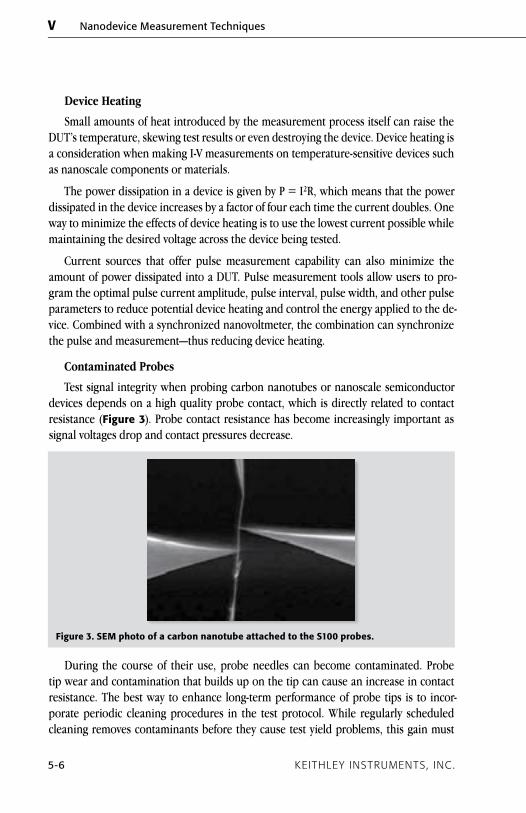
5-6 Keithley instruments, inc .
V Nanodevice Measurement Techniques
Device Heating
Small amounts of heat introduced by the measurement process itself can raise the DUT’s temperature, skewing test results or even destroying the device. Device heating is a consideration when making I-V measurements on temperature-sensitive devices such as nanoscale components or materials.
The power dissipation in a device is given by P = I2R, which means that the power dissipated in the device increases by a factor of four each time the current doubles. One way to minimize the effects of device heating is to use the lowest current possible while maintaining the desired voltage across the device being tested.
Current sources that offer pulse measurement capability can also minimize the amount of power dissipated into a DUT. Pulse measurement tools allow users to pro-gram the optimal pulse current amplitude, pulse interval, pulse width, and other pulse parameters to reduce potential device heating and control the energy applied to the de-vice. Combined with a synchronized nanovoltmeter, the combination can synchronize the pulse and measurement—thus reducing device heating.
Contaminated Probes
Test signal integrity when probing carbon nanotubes or nanoscale semiconductor devices depends on a high quality probe contact, which is directly related to contact resistance (Figure 3). Probe contact resistance has become increasingly important as signal voltages drop and contact pressures decrease.
Figure 3. SeM photo of a carbon nanotube attached to the S100 probes.
During the course of their use, probe needles can become contaminated. Probe tip wear and contamination that builds up on the tip can cause an increase in contact resistance. The best way to enhance long-term performance of probe tips is to incor-porate periodic cleaning procedures in the test protocol. While regularly scheduled cleaning removes contaminants before they cause test yield problems, this gain must

V Nanodevice Measurement Techniques
nanotechnology measurement handbooK 5-7
V
be weighed against its cost. One major cost element associated with cleaning is reduced test throughput while the probe system is out of service. Another consideration is that too little cleaning adversely affects test yields.
The necessity for Testing StandardsAs newer electronic devices are created using carbon nanotubes or other nanoscale
materials, the need for testing standards becomes more evident. Consistency in meas-urement technique and reporting of data is critical in order for new manufacturing processes to be consistent. Keithley Instruments worked closely with The Institute of Electrical and Electronics Engineers (IEEE) to create IEEE 1650™-2005, the world’s first measurement standard for the electrical characterization of carbon nanotubes. P1650 and future standards and recommended guidelines will permit semiconductor manu-facturers and materials manufacturers of carbon nanotubes and nanoscale materials to precisely manufacture and fabricate the next generation of electronic components.
ConclusionThis discussion focused on just a few of the measurement issues that the semicon-
ductor industry and nanotechnologists must confront and overcome when designing the next generation of electronic devices. Traditional measurement techniques can still be applied, but as the dimensions of the devices shrink and power limitations are in-creasingly of concern, the measurement techniques must be tailored so as to achieve the results one is expecting. New measurement tools are now becoming available that address the many issues. In addition, professional organizations must continue work-ing on developing new measurement standards so that the measurement results can be made, compared, and verified with confidence.

a g r e a t e r m e a s u r e o f c o n f i d e n c e
“To get a free electronic version of this book,
visit Keithley’s Knowledge
Center web page.”