nano express open access device and circuit-level performance
TRANSCRIPT

Tan et al. Nanoscale Research Letters 2012, 7:467http://www.nanoscalereslett.com/content/7/1/467
NANO EXPRESS Open Access
Device and circuit-level performance of carbonnanotube field-effect transistor withbenchmarking against a nano-MOSFETMichael Loong Peng Tan1,2*, Georgios Lentaris2 and Gehan AJ Amaratunga2
Abstract
The performance of a semiconducting carbon nanotube (CNT) is assessed and tabulated for parameters againstthose of a metal-oxide-semiconductor field-effect transistor (MOSFET). Both CNT and MOSFET models consideredagree well with the trends in the available experimental data. The results obtained show that nanotubes cansignificantly reduce the drain-induced barrier lowering effect and subthreshold swing in silicon channelreplacement while sustaining smaller channel area at higher current density. Performance metrics of both devicessuch as current drive strength, current on-off ratio (Ion/Ioff), energy-delay product, and power-delay product for logicgates, namely NAND and NOR, are presented. Design rules used for carbon nanotube field-effect transistors(CNTFETs) are compatible with the 45-nm MOSFET technology. The parasitics associated with interconnects are alsoincorporated in the model. Interconnects can affect the propagation delay in a CNTFET. Smaller lengthinterconnects result in higher cutoff frequency.
Keywords: Device modeling, HSPICE, Benchmarking, MOSFET, CNTFET, Logic gates
BackgroundCarbon nanotubes (CNTs) have been proposed as an alter-native channel material to silicon (Si), based on theirquantum transport properties which, in principle, allowballistic transport at room temperature. CNT ballistic mod-eling [1] has been used to assess the performance of thedevice at the HSPICE circuit level [2]. Device modeling isvital for projecting the practical performance of a CNTtransistor as a switching device in integrated circuits (ICs).We report the potential of a CNTchannel through mod-
eling as a substitute to a silicon channel in a scaled metal-oxide-semiconductor field-effect transistor (MOSFET) forlogic applications. By scaling the Si transistor and thedensity of states (DOS) of the CNT, we observe goodagreement between CNT and ballistic Si MOSFET [3] inthe drain current–voltage (I-V) output characteristics.Output current is critical in determining the switchingspeed of a transistor in logic gates. We show that the
* Correspondence: [email protected] of Electrical Engineering, Universiti Teknologi Malaysia, UTM Skudai,Johor 81310, Malaysia2Electrical Engineering Division, University of Cambridge, 9 J.J. Thomson Ave,Cambridge CB3 0FA, UK
© 2012 Tan et al.; licensee Springer. This is an OAttribution License (http://creativecommons.orin any medium, provided the original work is p
output performances of CNT and Si channel devices aresimilar in the 45-nm node experimental data. However,the modeling results point to significant reduction indrain-induced barrier lowering (DIBL) and related highfield effects in the CNT compared to the short-channelnanoscale Si MOSFET at the same output current. Wealso assess the effect of channel area restructuring on elec-tric field properties as well as the role of the DOS in deter-mining CNT current. Unlike in the Si MOSFET, it is seenthat the performance of a CNT channel is enhanced whenthe source/drain width is minimized rather than the chan-nel length due to gate-to-source/drain parasitic fringecapacitances. MOSFET scaling according to Moore's law islimited by process controllability.
MethodsCarbon nanotube and MOSFET modelingA layout of a carbon nanotube field-effect transistor(CNTFET) is shown in Figure 1. The area of the channelis defined by the width (W) of the source and drain con-tacts and the length (L) of the nanotube. Details of theballistic MOSFET modeling can be found in our previouswork [3].
pen Access article distributed under the terms of the Creative Commonsg/licenses/by/2.0), which permits unrestricted use, distribution, and reproductionroperly cited.

Top Gate
Channel Length LSource Drain
Contact
ContactVia
C
ChannelWidth W
ContactWidth WC
S
ContactVia
Carbon Nanotube
Contact Length LC
Figure 1 Top view of CNTFET device.
10
12
14
16VG = 0.0
VG = 0.2
VG = 0.4
VG = 0.6
Tan et al. Nanoscale Research Letters 2012, 7:467 Page 2 of 10http://www.nanoscalereslett.com/content/7/1/467
The analytical carbon nanotube model comes from thework of Rahman et al. [4,5] where we have extended theuniversal DOS spectral function into a numerical calcu-lation for CNT conduction subbands. We have modifiedthe DOS subroutine [6] to account for multimode trans-port [7]. To improve precision and accuracy in the simu-lation, the parameters in Table 1 for MOSFET andCNTFET which incorporate quasi-ballistic transportscattering are extracted from CADENCE [8] and Javeyet al. [9], respectively. CNTFET analytical models havebeen validated and agree well with experimental data[9,10] particularly in the saturation region depicted inFigure 2.If a CNT can achieve the same current as a MOSFET,
an identical channel area (AMOS =ACNT) can be main-tained by setting the width of the physical space occu-pied by the CNTFET to be WCNT =AMOS / LCNT. WhenW= L for the MOSFET, the general channel area can beexpressed as A= (kL)2, where k is the scaling factor. Assuch, a CNT channel with length, 2kL should attain thesame current with W= 0.5kL. Thus, if the physical widthof the CNT channel is W≤ 0.5kL, there will not be anyarea drawback in output current due to the longer L. Infact, the maximum electric field in CNT is halved, givingEmCNT =EmSi / 2, and is significantly reduced as the CNT
Table 1 Source and drain capacitance for multiplesubstrate insulator thickness
Substrate insulatorthickness (nm)
Csb or Cdb (aF) Ids (μA) at VG =1 V
10 34.53 47.395
50 6.906 47.340
100 3.453 47.272
200 1.727 47.135
300 1.151 46.998
400 0.863 46.860
500 0.691 46.723
channel grows longer. For a CNT with L= 60 nm com-pared to a Si MOSFET with L= 45 nm, the maximumelectric field is Em= 0.83 EmSi.
Device modelingThe top view of CNTFET with the source and drain con-tacts is shown in Figure 1. The filled black rectanglerepresents the contact enclosure with dimensionextracted from a generic 45-nm MOSFET process designkit (PDK) where S= 20 nm, C= 60 nm, andWC = LC = 100 nm. Nine capacitances are introduced intothe carbon-based macromodel as illustrated in Figure 3.They are the gate oxide capacitance Cox, quantum capaci-tance CQ, source capacitance Cs, drain capacitance Cd,substrate capacitance Csub, source-to-bulk capacitanceCsb, drain-to-bulk capacitance Cdb, gate-to-source capaci-tance Cgs, and gate-to-drain capacitance Cgd. The size ofthe contact is crucial as it ultimately influences Csb
and Cdb. They are given in Table 1 and can be written as
0 0.1 0.2 0.3 0.4 0.50
2
4
6
8
VDS
(Volt)
I DS (
A)
VG = 0.8
VG = 1.0
µ
Figure 2 Simulated CNT drain characteristic versus 80-nmexperimental data. Simulated single-subband CNT draincharacteristic (solid lines) versus 80-nm experimental data withhigh-potassium (K)-doped source and drain doping (filled diamond)at VG = 0 to 1.0 V in 0.2-V steps. (Adapted from [9]).

Contact Contact
Drain
Gate
Insulator
Carbon nanotube
Insulator
Substrate
Source
Vs
VG
Cgs
Cs
Cgd
Cox
CQ
CsbCsub
CdVd
Cdb
VsUB
Figure 3 HSPICE macromodel for CNTFET.
Tan et al. Nanoscale Research Letters 2012, 7:467 Page 3 of 10http://www.nanoscalereslett.com/content/7/1/467
Csb or Cdb ¼ εinsWLtins
� �; ð1Þ
where tins is the thickness of the insulator, W is the widthof the contact, L is the length of the contact, and εins isthe permittivity of the insulator. The substrate insulatorcapacitance Csub for CNTFET is given by
Csub CNTFET ¼ 2πεinsln 4tsub
d
� � ; ð2Þ
where tsub is the substrate oxide thickness and d isthe diameter of CNT. The intrinsic gate capacitanceCG of CNTFET is a series combination of gate oxidecapacitance Cox and quantum capacitance CQ [11].The Cox of a CNTFET [12-14] is shown to be
Nanotube Cox ¼ 2πεinsln 2tinsþd
d
� � ð3Þ
The quantum capacitance is expressed by [15-17]
CQ ¼ 2gvgsq2
hvF
Xi
EffiffiffiffiffiffiffiffiffiffiffiffiffiffiffiffiffiffiffiffiffiffiffiffiffiffiffiffiE2 � EGi=2ð Þ2
q Θ Ej j � EGi
2
� �;
ð4Þ
where gs is the spin degeneracy, gv is the valley degener-acy, EGi is the bandgap energy, and vF is the Fermi vel-ocity. The step function Θ xð Þ is equal to 1 when x > 0and 0 when x < 0. The Cgs and Cgd are given as
Cgs ¼ LgCox
2CQ þ Cs
Ctot þ CQ
� �; ð5Þ
Cgd ¼ Lg2Cox
CQ þ Cd
Ctot þ CQ
� �; ð6Þ
where Cs and Cd are the source and drain capacitance fit-ting parameters, respectively, [1,2] that are used to fit the
experimental data and Lg is the length of the gate. Thesum of Cgd and Cdb gives the intrinsic capacitance Cint.The square law is no longer valid for I-V formulation
of short-channel MOSFET. Tan et al. [3] succinctly showthe transformation of the square law that applies for thelong channel to the linear law that is applicable forshort-channel MOSFET. On the other hand, I-V formu-lation for the CNTFET model follows the quantum con-ductance principle that was developed by Rahman et al.[4,5] and Datta [6]. The I-V model can be rewritten interms of drain voltage Vd, source voltage Vs, and gatevoltage VG that is expressed by
Ids VG;Vd;Vsð Þ ¼ GONkBTq
� log 1þ exp q EF � Vsc VG;Vd;Vsð Þð Þ=kBTð Þð Þ½ �� GON
kBTq
log 1þ exp q EF � Vsc VG;Vd;Vsð Þððð½�Vd � VsÞ=kBTÞÞ�; ð7Þ
where GON is the ON-conductance, Vsc is also known asthe channel surface potential [11], EF is the Fermi en-ergy, kB is the Boltzmann constant, T is the temperature,and q is the electric charge. The equation is iterativelysolved and hence includes the effect of gate voltage.
Model verificationIn this section, the potential of CNT circuit design isassessed. Our simulation results in Figure 4 indicatethat CNTFET is able to provide drain current perform-ance comparable to a 45-nm-gate length MOSFET.The model is successful in predicting expected outputcurrent levels in a sub-100-nm-channel CNT transistorexperimental data. The DIBL effects and subthresholdswing (SS) are better suppressed in the CNT device,while the Si transistor demonstrates a moderate DIBL

µ
0 0.1 0.2 0.3 0.4 0.5 0.6 0.7 0.8 0.9 10
10
20
30
40
50
VDS
(Volt)
I DS (
A)
0 0.2 0.4 0.6 0.8 10
1020304050
I DS
(A
)
VDS (V)
MOSFET
Metallic
Semiconducting
µ
Figure 4 I-V characteristic of SWCNT model, semiconducting andmetallic CNT experimental data. I-V characteristic of a 50-nmSWCNT model (dotted lines) demonstrated in comparison toL� 50 nm semiconducting CNT experimental data (filled diamond).Metallic CNT experimental data are also shown (filled circle). Insetshows 45-nm MOSFET characteristics where the dimension is givenin Table 2. Initial VG at the top for CNT and MOSFET is 1 V with 0.1-Vsteps. (Adapted from [10]).
Tan et al. Nanoscale Research Letters 2012, 7:467 Page 4 of 10http://www.nanoscalereslett.com/content/7/1/467
and SS due to short-channel effects as shown inTable 2. Although the CNT has similar ON-current, itsustains Ion/Ioff ratio of two orders of magnitude lowerthan Si MOSFET. The quantum ON-conductance limit
Table 2 Device model specification at VGS = 1 V
Parameter CNTFET benchmarking
CNTFET MOSFET
Channel length, L 50 nm 45 nm
Contact width, Wcontact 100 nm -
Channel width, W - 125 nm
Channel area 5 × 10⁻¹⁵ m2 5.63 × 10⁻¹⁵ m2
Nanotube diameter 1.5437 nm -
Chiral vector [n,m] [20,0] -
Maximum current, Idmax 46.56 μA 50.20 μA
Transconductance, gm 68.1 μS 148 μS
Carrier density, Idmax / [d or W] 30.16 μA/nm 0.40 μA/nm
Gate capacitance, CG 14.85 aF 65.8 aF
Drain capacitance, Cd 0.59 aF 19.0 aF
Source capacitance, Cs 1.43 aF 78.7 aF
Substrate capacitance, Csub 1.60 aF 6.52 aF
Total terminal capacitance, Cter 18.47 aF 209.02 aF
Intrinsic capacitance, Cint=Cgd+Cdb 21.29 aF 37.40 aF
Load capacitance, CL at 1 GHz 46.54 fF 50.13 fF
Cutoff frequency with 5-μm wire 13.57 GHz 27.72 GHz
Drain-induced barrier lowering 40.85 mV/V 83.89 mV/V
Subthreshold swing 72.3 mV/decade 113.67 mV/decade
On-off ratio 2.99 × 10⁴ 9.54 × 10⁶
of a ballistic single-walled carbon nanotube (SWCNT)and graphene nanoribbon with perfect contact isGON= 4e2/h and GON= 2e2/h (twice the fundamentalquantum unit of conductance), respectively. Quantumcapacitance CQ is directly proportional to the densityof states of the semiconductor but inversely propor-tional to the electrochemical potential energy. WhenCQ becomes smaller than Cox, a large quantity of theelectrochemical potential energy is needed to occupythe states above the Fermi energy. This results in thereduction in overall intrinsic gate capacitance CG andlimits the channel charge in a semiconductor and ul-timately the I-V characteristic of the FET devices.Comparison in Table 2 shows that MOSFET has ahigher cutoff frequency due to higher transconductanceas compared to CNTFET with lower capacitances.First, MOSFET logic circuits are built based on a 45-nm
generic PDK. The MOSFET designs are then comparedwith carbon-based circuit models that consist of prototypedigital gates implemented in HSPICE circuit simulator.These CNTFETs use 45-nm process design rules, namelythe minimum contact size. For a fair assessment, bothMOSFET and CNTFET are designed to provide similarcurrent strength (�46 to 50 μA).An appropriate CNTFET device was fabricated to inves-
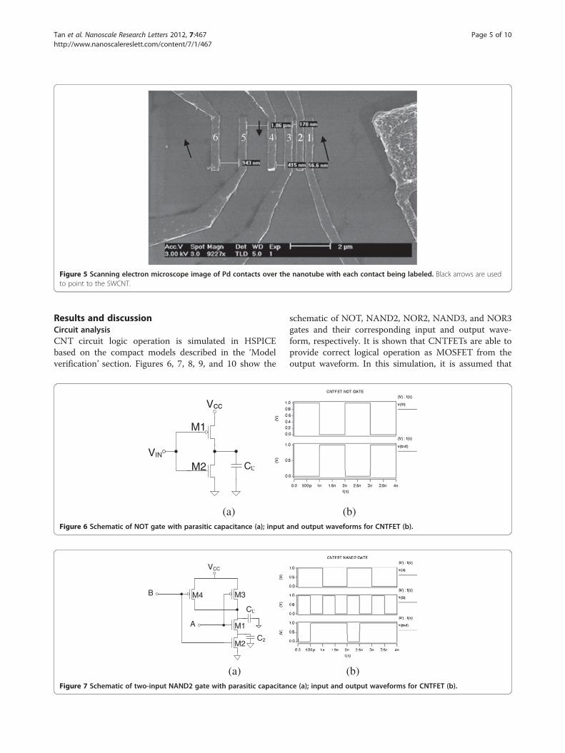
tigate the contact resistance. SWCNTs were grown in situusing the bimetal catalyst iron-molybdenum (Fe-Mo) [11]on a silicon-on-insulator substrate with 200 nm of ther-mally grown SiO2. Metal contacts were patterned by elec-tron beam lithography, and 60 nm of palladium (Pd)contacts was deposited to form a back gate geometry tran-sistor. The spacing between the Pd contacts varied be-tween 56.6 nm and 1.06 μm as shown in Figure 5.A four-probe measurement was carried out at room
temperature to extract the resistance characteristics of thecarbon nanotube that was used to form the transistorchannel. The normalized resistances were 0.495, 0.744,0.118, and 0.450 MΩ/nm for R2,3, R2,4, R3,4, and R4,5, re-spectively, where indices indicate Pd contact labels. Thediameter of the SWCNT is 1.5 nm. Calculation shows thatthe 415-nm nanotube resistance is 27.8 kΩ that is almostequal to the theoretical RON=h/q2 = 25.812 kΩ and fourtimes larger than the theoretically lowest quantum resist-ance of the SWCNT, RON=h/4q2 = 6.5 kΩ.Though at 415-nm channel length ballistic transport is
not preserved in the CNT, it is still only factor 4 largerthan the theoretically expected minimum, suggesting thatscattering is not extensive. Nevertheless, the model whichassumes ballistic transport predicts similar saturationcurrent levels (�50 μA) for both the 50- and 415-nmchannel devices, as illustrated in Figure 5. Practically, thissuggests that one must have CNT channel lengths belowapproximately 100 nm or even low contact resistance inorder to utilize ballistic transport in them.
56 23 14 1
Figure 5 Scanning electron microscope image of Pd contacts over the nanotube with each contact being labeled. Black arrows are usedto point to the SWCNT.
Tan et al. Nanoscale Research Letters 2012, 7:467 Page 5 of 10http://www.nanoscalereslett.com/content/7/1/467
Results and discussionCircuit analysisCNT circuit logic operation is simulated in HSPICEbased on the compact models described in the ‘Modelverification’ section. Figures 6, 7, 8, 9, and 10 show the
VIN
Vcc
CL’M2
M1
(a) Figure 6 Schematic of NOT gate with parasitic capacitance (a); input a
(a)
B
A
M4 M3
M1
M2
VCC
CL’
C2
Figure 7 Schematic of two-input NAND2 gate with parasitic capacitan
schematic of NOT, NAND2, NOR2, NAND3, and NOR3gates and their corresponding input and output wave-form, respectively. It is shown that CNTFETs are able toprovide correct logical operation as MOSFET from theoutput waveform. In this simulation, it is assumed that
(b) nd output waveforms for CNTFET (b).
(b)ce (a); input and output waveforms for CNTFET (b).

(a) (b)
A B C
VCC
CL’
C2
C1
M5 M6
M3
M2
M1
M4
Figure 9 Schematic of three-input NAND3 gate with parasitic capacitance (a); input and output waveforms for CNTFET (b).
(a) (b)
B
A
M4 M3
M2
M1
VCC
CL’
C2
Figure 8 Schematic of two-input NOR2 gate with parasitic capacitance (a); input and output waveforms for CNTFET (b).
Tan et al. Nanoscale Research Letters 2012, 7:467 Page 6 of 10http://www.nanoscalereslett.com/content/7/1/467
both the n-type and p-type CNTFETs have symmetricalI-V characteristics. The performance evaluation of theseBoolean operations is listed in Table 3.
Performance evaluationThe unity current gain cutoff frequency for the CNTFETcircuit model is depicted in Figure 11. The model uses a
(a)
c
B
M6 M5 M4
M3
M2
M1A
VCC
C1
C2
CL’
Figure 10 Schematic of three-input NOR3 gate with parasitic capacita
copper interconnect of 45 nm with a 100-nm and 500-nm substrate insulator thickness. The interconnectlength varies from 0.01 to 100 μm. The length of inter-connects affects considerably the frequency response.The lower length interconnect enhances the cutoff fre-quency. The substrate thickness also plays an active rolein lower length domain. No distinction with the substrate
(b)nce (a); input and output waveforms for CNTFET (b).

INV NAND2 NAND3 NOR2 NOR310
-22
10-20
10-18
10-16
10-14
10-12
Logic Gates
Po
wer
Del
ay P
rod
uct
MOSFET (tnode
= 45 nm)
CNTFET (Lwire
= 5 m , tsub
= 500 nm)
CNTFET (Lwire
= 1 m , tsub
= 500 nm)
CNTFET (Lwire
= 0 m , tsub
= 500 nm)
µ
µ
µ
Figure 12 PDP of CNTFET versus MOSFET.
Table 3 45-nm process propagation delay computationbetween CNTFET (with and without interconnect) andMOSFET (post-layout simulation)
Logiccircuits
CNTFET with 45-nmprocess design guidelines
MOSFET with 45-nmprocess
Delay withoutinterconnects
Delay with 5-μminterconnect
Delay (post-layoutsimulation)
Propagationdelay,
Propagationdelay,
Propagationdelay,
tp (ps) tp (ps) tp (ps)
NOT 0.14 9.277 5.005
NAND2 0.39 12.97 8.719
NAND3 0.61 16.87 11.343
NOR2 0.47 12.98 8.797
NOR3 0.50 16.48 11.655
Tan et al. Nanoscale Research Letters 2012, 7:467 Page 7 of 10http://www.nanoscalereslett.com/content/7/1/467
thickness is visible beyond 1-μm interconnect length. Thefigure of merit for logic devices, namely power-delay prod-uct (PDP) and energy-delay product (EDP) metrics, aregiven as
PDP ¼ Pav
�tp;ð8Þ
EDP ¼ PDP�tp;
ð9Þ
where Pav is the average power and tp is the propagationdelay.Figure 12 shows the PDP of CNTFET and MOSFET
logic gates for the 45-nm process. The simulationresults show that the PDP of CNTFET-based gates are
10-2
10-1
100
101
102
0
50
100
150
200
250
300
350CNTFET
Length of Interconnect (µm)
Cut
off F
requ
ency
(G
Hz)
45 nm node, A=10.0 fm 2, tsub
= 500 nm
45 nm node, A=10.0 fm 2, tsub
= 100 nm
Figure 11 Cutoff frequency for CNTFET. Cutoff frequency forCNTFET with interconnect length from 0.01 to 100 μm with a sourceand drain contact area equivalent to that of a 45-nm MOSFET andsubstrate insulator thickness of 100-nm and 500-nm.
lower than that of MOSFET-based gates by severalorders of magnitude [18]. For the 45-nm process, the PDPof CNTFET-based gates is two times smaller than that ofMOSFET-based gates with Lwire = 5 μm. It increases to1,000 times without interconnect (Lwire = 0 μm).Figure 13 shows the EDP of CNTFET and MOSFET
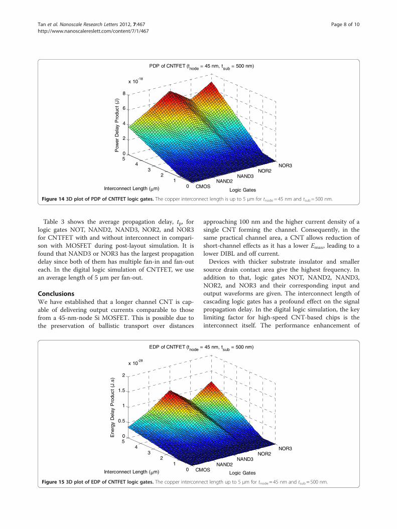
logic gates for the 45-nm process. EDP for CNTFET-based gates with 5 μm is comparable to MOSFET. Asa result, the wire length should be kept shorter than5 μm in order to obtain energy-efficient low-powerarchitecture.Figures 14 and 15 show 3D plots of PDP and EDP for
CNTFET with copper interconnect up to 5 μm in length.We observe a 28 % improvement of PDP while EDPreduces by 39 % for NAND3 that adopts the 45-nmprocess compared to the one that uses the 90-nmprocess contact size.
INV NAND2 NAND3 NOR2 NOR310
-36
10-32
10-28
10-24
10-20
10-16 EDP of CNTFET and MOSFET (45nm Process)
Logic Gates
En
erg
y D
elay
Pro
du
ct
MOSFET (tnode
= 45 nm)
CNTFET (Lwire
= 5 m , tsub
= 500 nm)
CNTFET (Lwire
= 1 m , tsub
= 500 nm)
CNTFET (Lwire
= 0 m , tsub
= 500 nm)
(J.s
)
µ
µ
µ
Figure 13 EDP of CNTFET versus MOSFET.
CMOS NAND2
NAND3NOR2
NOR3
01
23
450
2
4
6
8
x 10-18
Logic Gates
PDP of CNTFET (tnode = 45 nm, tsub = 500 nm)
Interconnect Length ( m)
Pow
er D
elay
Pro
duct
(J)
µ
Figure 14 3D plot of PDP of CNTFET logic gates. The copper interconnect length is up to 5 μm for tnode = 45 nm and tsub = 500 nm.
Tan et al. Nanoscale Research Letters 2012, 7:467 Page 8 of 10http://www.nanoscalereslett.com/content/7/1/467
Table 3 shows the average propagation delay, tp, forlogic gates NOT, NAND2, NAND3, NOR2, and NOR3for CNTFET with and without interconnect in compari-son with MOSFET during post-layout simulation. It isfound that NAND3 or NOR3 has the largest propagationdelay since both of them has multiple fan-in and fan-outeach. In the digital logic simulation of CNTFET, we usean average length of 5 μm per fan-out.
ConclusionsWe have established that a longer channel CNT is cap-able of delivering output currents comparable to thosefrom a 45-nm-node Si MOSFET. This is possible due tothe preservation of ballistic transport over distances
CM01
23
450
0.5
1
1.5
2
x 10-28
EDP of CNTFET (tnode =
Interconnect Length ( m)
Ene
rgy
Del
ay P
rodu
ct (
J.s)
µ
Figure 15 3D plot of EDP of CNTFET logic gates. The copper interconne
approaching 100 nm and the higher current density of asingle CNT forming the channel. Consequently, in thesame practical channel area, a CNT allows reduction ofshort-channel effects as it has a lower Emax, leading to alower DIBL and off current.Devices with thicker substrate insulator and smaller
source drain contact area give the highest frequency. Inaddition to that, logic gates NOT, NAND2, NAND3,NOR2, and NOR3 and their corresponding input andoutput waveforms are given. The interconnect length ofcascading logic gates has a profound effect on the signalpropagation delay. In the digital logic simulation, the keylimiting factor for high-speed CNT-based chips is theinterconnect itself. The performance enhancement of
OS NAND2
NAND3NOR2
NOR3
Logic Gates
45 nm, tsub = 500 nm)
ct length up to 5 μm for tnode = 45 nm and tsub = 500 nm.
Tan et al. Nanoscale Research Letters 2012, 7:467 Page 9 of 10http://www.nanoscalereslett.com/content/7/1/467
these carbon-based material is negligible if the intercon-nect capacitance is not reduced significantly with transis-tor feature size. Bundled metallic MWCNTs are seenas a potential candidate to replace copper interconnectsas future IC interconnects once the challenges of inte-grating CNT interconnects onto existing manufacturingprocesses are met.We also show that ballistic transport is not maintained
in a CNT when contact resistance is large. A good fit tothe data output characteristics from a 50-nm CNT chan-nel device is obtained. As mean free path in a CNT isvery long, often exceeding 1 μm, the ballistic processplays a predominant role, similar to one discussed exten-sively by Riyadi and Arora [19]. In fact, they define anew feature, named ballisticity. The truly ballistic trans-port is possible as channel length approaches zero. In afinite length, there are always finite probabilities ofscattering.
Competing interestsThe authors declare that they have no competing interests.
Authors’ contributionsMLPT designed and carried out the device modeling and simulation work,analyzed the data, and drafted the manuscript. GL carried out theexperimental work and fabricated the SWCNT. GAJA supervised the researchwork and helped amend the manuscript. All authors read and approved thefinal manuscript.
Authors’ informationsMLPT was born in Bukit Mertajam, Penang, Malaysia, in 1981. He received hisB. Eng. (electrical-telecommunication) and M. Eng. (electrical) degrees fromUniversiti Teknologi Malaysia (UTM), Skudai, Malaysia, in 2003 and 2006,respectively. He conducted his postgraduate research in nanoscale MOSFETmodeling at the Intel Penang Design Center, Penang, Malaysia. He recentlyobtained his Ph.D. degree in 2011 at the University of Cambridge,Cambridge, UK. He is a senior lecturer at UTM. His present research interestsare in device modeling and circuit simulation of carbon nanotube, graphenenanoribbon, and MOSFET. MLPT is an IEEE member, member of IET (MIET),graduate member of IEM (GRAD IEM), and member of Queens' College. GLwas born in Chania, Crete, Greece in 1983. He holds a B. Eng. (computingand robotic systems) degree from the Department of Electric Engineering inLiverpool University and a Ph.D. degree in engineering from the University ofCambridge. His Ph.D. thesis was in the area of fabricating and characterizingsingle-walled carbon nanotubes and ZnO nanowire transistors and sensors.He has also worked as a researcher at Nokia's Eurolab between 2009 and2011 and particularly in developing novel sensors as part of Nokia'sNanosensing group. He, as part of Cambridge-M.I.T i-Teams, examines,identifies, and analyzes commercial potentials for an Intelligent Textbooktechnology, which uses an artificial intelligence engine, with real targetcustomers in relevant industries. At present, GL is interested in pursuing acareer that combines technology and analytical expertise, veiled in abusiness management environment. He is a member of Churchill College.GAJA received his B.Sc. degree in electrical/electronic engineering fromCardiff University, Wales, UK, in 1979 and his Ph.D. degree in electrical/electronic engineering from the University of Cambridge, Cambridge, UK, in1983. He has held the 1966 Professorship in Engineering with the Universityof Cambridge since 1998. He currently heads the Electronics, Power andEnergy Conversion Group, one of four major research groups within theElectrical Engineering Division of the Cambridge Engineering Faculty. He hasworked for 25 years on integrated and discrete electronic devices for powerconversion and on the science and technology of carbon-based electronicsfor 22 years. He has an active research program on the synthesis andelectronic applications of carbon nanotubes and other nanoscale materials.He also has research interest in nanomagnetic materials for spin transportdevices. He currently sits on the steering committee of the Nokia-Cambridge
University Strategic Collaboration on Nanoscience and Nanotechnology andis the head of the Nokia-CU Nanotechnology for Energy Programme. Hiscurrent research is focused on integrated power conversion circuits. He haspreviously held faculty positions at the University of Liverpool (Chair inElectrical Engineering), University of Cambridge, and University ofSouthampton. He has held the UK Royal Academy of Engineering OverseasResearch Award at Stanford University, Stanford, CA, USA, and been a RoyalSociety visitor at the School of Physics, University of Sydney, Sydney, NewSouth Wales, Australia. He has published over 450 journal and conferencepapers. GAJA was elected a Fellow of the Royal Academy of Engineering in2004. In 2007, he was awarded the Royal Academy of Engineering SilverMedal ‘for outstanding personal contributions to British engineering.’
AcknowledgmentsMLPT thanks the Ministry of Higher Education Malaysia and the UniversitiTeknologi Malaysia (UTM) for the award of advanced study fellowshipleading to a Ph.D. degree at the University of Cambridge. This work ispartially supported by a New Academic Staff (NAS) research grant (vot no.: R.J130000.7723.4P030) and the UTM Research University Grant (GUP) (vot no.:Q.J130000.2623.05J42). The authors also gratefully acknowledge thesuggestions made by anonymous reviewers that have enhanced the qualityof the manuscript greatly.
Received: 29 June 2012 Accepted: 9 August 2012Published: 19 August 2012
References1. Deng J, Wong HSP: A compact SPICE model for carbon-nanotube field-
effect transistors including nonidealities and its application - part I:model of the intrinsic channel region. IEEE Trans Electr Dev 2007,54:3186–3194.
2. Guo J, Datta S, Lundstrom B, McEuen P, Javey A, Dai H, Kim H, McIntyre P:Assessment of silicon MOS and carbon nanotube FET performance limitsusing a general theory of ballistic transistors. IEDM Technical Digest 2002,2002:711–714.
3. Tan MLP, Arora VK, Saad I, Ahmadi MT, Ismail R: The drain velocityovershoot in an 80 nm metal-oxide-semiconductor field-effect transistor.Journal of Applied Physics 2009, 105:7.
4. Rahman A, Guo J, Datta S, Lundstrom MS: Theory of ballisticnanotransistors. IEEE Transactions on Electron Devices 2003, 50:1853–1864.
5. Rahman A, Wang J, Guo J, Hasan MS, Liu Y, Matsudaira A, Ahmed SS, DattaS, Lundstrom M: http://nanohub.org/resources/fettoy.
6. Datta S: Quantum Transport: Atom to Transistor. Cambridge: CambridgeUniversity Press; 2006.
7. Appenzeller J, Knoch J, Radosavljevicacute M, Avouris P: Multimodetransport in Schottky-barrier carbon-nanotube field-effect transistors.Physical Review Letters 2004, 92:226802.
8. GPDK045 - 45 nm Generic: (Revision 2.0) https://pdk.cadence.com/home.do.9. Javey A, Tu R, Farmer DB, Guo J, Gordon RG, Dai H: High performance
n-type carbon nanotube field-effect transistors with chemically dopedcontacts. Nano Letters 2005, 5:345–348.
10. Javey A, Guo J, Paulsson M, Wang Q, Mann D, Lundstrom M, Dai H:High-field quasiballistic transport in short carbon nanotubes. PhysicalReview Letters 2004, 92:106804.
11. Kshirsagar C, El-Zeftawi MN, Banerjee K: Analysis and implications of parasiticand screening effects on the high-frequency/RF performance of tunneling-carbon nanotube FETs. In Proceedings of the DAC: 45th ACM/IEEE DesignAutomation Conference, 2008: June 8–13 2008; Anaheim. New York: ACM/IEEE 2008, 2008:250–255.
12. Kazmierski TJ, Dafeng Z, Al-Hashimi BM: HSPICE implementation of anumerically efficient model of CNT transistor. In Proceedings of the: FDL2009 Forum on Specification & Design Languages: Sept 22–24 2009; SophiaAntipolis. Gières: ECSI 2009, 2009:1–5.
13. Rosenblatt S, Yaish Y, Park J, Gore J, Sazonova V, McEuen PL: Highperformance electrolyte gated carbon nanotube transistors. Nano Letters2002, 2:869–872.
14. Shimotani H, Kanbara T, Iwasa Y, Tsukagoshi K, Aoyagi Y, Kataura H: Gatecapacitance in electrochemical transistor of single-walled carbonnanotube. Appl Phys Lett 2006, 88:073104.

Tan et al. Nanoscale Research Letters 2012, 7:467 Page 10 of 10http://www.nanoscalereslett.com/content/7/1/467
15. Ilani S, Donev LAK, Kindermann M, McEuen PL: Measurement of thequantum capacitance of interacting electrons in carbon nanotubes. NatPhys 2006, 2:687–691.
16. Fang T, Konar A, Xing H, Jena D: Carrier statistics and quantumcapacitance of graphene sheets and ribbons. Appl Phys Lett 2007,91:092109.
17. Xia J, Chen F, Li J, Tao N: Measurement of the quantum capacitance ofgraphene. Nat Nano 2009, 4:505–509.
18. Cho G, Kim Y-B, Lombardi F: Assessment of CNTFET based circuitperformance and robustness to PVT variations. In Proceedings of theMWSCAS '09 52nd IEEE International Midwest Symposium on Circuits andSystems: August 2–5: Cancun. New York: IEEE 2009, 2009:1106–1109.
19. Riyadi MA, Arora VK: The channel mobility degradation in a nanoscalemetal-oxide-semiconductor field effect transistor due to injection fromthe ballistic contacts. Journal of Applied Physics 2011, 109:056103.
doi:10.1186/1556-276X-7-467Cite this article as: Tan et al.: Device and circuit-level performance ofcarbon nanotube field-effect transistor with benchmarking against anano-MOSFET. Nanoscale Research Letters 2012 7:467.
Submit your manuscript to a journal and benefi t from:
7 Convenient online submission
7 Rigorous peer review
7 Immediate publication on acceptance
7 Open access: articles freely available online
7 High visibility within the fi eld
7 Retaining the copyright to your article
Submit your next manuscript at 7 springeropen.com