n94-18379 - nasa · n94-18379 13.1.1 a special ... in developing such a compiler besides achieving...
TRANSCRIPT

3rd NASA Symposium on VLSI Design 1991
N94-1837913.1.1
A Special Purpose Silicon CompilerFor Designing Supercomputing VLSI Systems
* N.Venkateswaran,P.Murugavel,V.Kamakoti,M.J.ShankarRaman,S.Rangar ajan,
M.Mallikarjun,B .Karthikeyan,T.S .Prabhakar,V.Satish,P.R.Venkat asubramaniam,
R. Sivakum ar,R. S rinivas an,S. C h an dr asekh ar, G. Sur esh, M. B.K art hikeyan,
S.Ramachandran,S.Sankar,P.V.Balaji,P.Kishore
** F.Lawrence,S.Pattabiraman,G.Suresh,V.Arun Shankar,A.Ashraf, V.Balaji,
M.Balaji,Sunil.K,R.Devanathan,Y.Eliyas,K.Krishnan,B.Krishna Kumar,
B.Kumaran,N.Rajesh & G.Vijay Venkatesh
**Department of Computer Science and Engineering.
Sri Venkateswara College of Engineering
University of Madras
Nazarethpet, Madras 602 103, India.
Abstract- Design of general/special purpose Supereomputing VLSI systems for
numeric algorithm execution involves tackling two important aspects namely
their computational and eommunleatlon complexities. Development of soft-
ware tools for designing such systems itself becomes complex. Hence a novel
design methodology has to be developed. For designing such complex systems
a speeial purpose silleon compiler is needed in which
1. The computational and communieatlonal structures of different numeric
algorithms should be taken into account to simplify the silicon compiler
design.
2. The approach is maerocell based.
3. The software tools at different levels,algorithm down to the VLSI circuit
layout_ should get integrated.
In this paper a special purpose silicon (SPS) compiler based on PACUBE
macrocell VLSI ARRAYS [1] for designing supercomputing VLSI systems is
presented. It is shown that turn-around-time and silicon real estate get reduced
over the silicon compilers based on PLAs_SLAs and gate arrays.
Characteristics 1 and 2 above enable the SPS compiler to perform systolic
mapping (at the macrocell level) of algorithms whose computational structures
are of GIPOP (Generalized Inner Product Outer Product) form [2]. Direct
systolic mapping on PLAs_ SLAs and gate arrays is very difficult as they are
micro-cell based. A novel GIPOP processor is under development using this
special purpose silicon compiler.
* pursuing their higher studies/employed in India or abroad. Contact for communication regarding thispaper N.Venkateswaran, Additional Professor, Dept of Computer Science and Engineering, Sri VenkateswaraCollege of Engineering,University of Madras,India. Authors j names listed randomly.
https://ntrs.nasa.gov/search.jsp?R=19940013906 2018-06-17T07:30:28+00:00Z

13.1.2
1 Introduction
No silicon compiler has yet been developed exclusively for tackling the complexity in de-
signing supercomputing VLSI systems. In developing such a compiler besides achieving re-
duced turn-around-time and area, computational performance of mapped functional units
and architectural characteristics like systolic mapping should also be considered. The latter
two factors are not taken care of in micro-cell based silicon compilers.
In conventional compilers the software tools are not integrated from algorithm down to
the VLSI circuit level. The integration of software tools at different levels can be achieved
by adopting novel methodologies in designing supercomputing VLSI systems (processors
and arrays) and developing novel algorithm mapping techniques. This integration reduces
the software complexity to a great extent.
The turn-around-time is high if gate arrays, PLAs and SLAs are employed for super-
computing system synthesis. Furth_t_e :silicon compilation should take place at a much
higher level than at the gate or the micro-ceU level for supercomputlng system design.
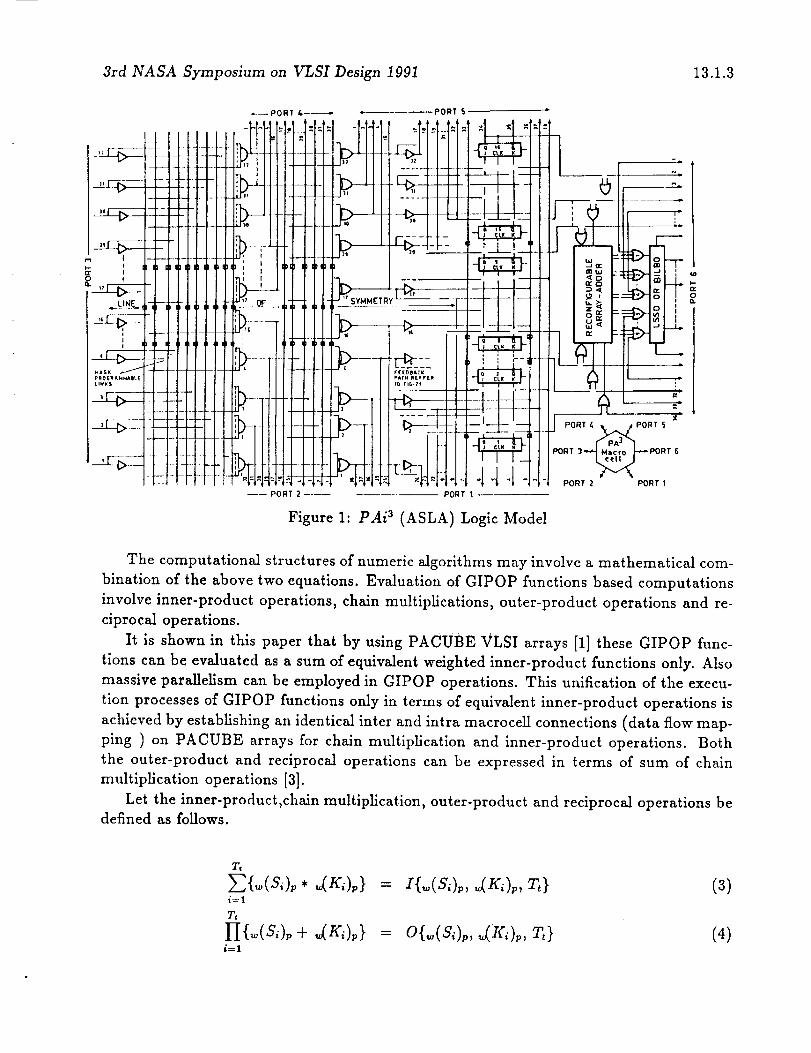
The PACUBE macro-cell structure is a combination of PLAs, SLAs,gate arrays and
standard cells.B%side s_storage and logic elements an important computing unit,the DRAA
(Dynamically Reconfigurabie Array Adder [1] ) is also present (Fig 1). The presence of tlae
DRAA reduces the turn-around-time and silicon area drastically for designing special pur-
pose VLSI systems. =The DRAA helps _ achieving h lgh performance due to-its functional
and architectural characteristics. If the DRAA were to be mapped on to PLAs, SLAs
and gate arrays the performance w_ get degraded.The special purpose silicon compiler
built for mapping supercomputing systems on the PACUBE arrays achieves all the above
factors.
2 PACUBE Macrocell Array And Systolic Mapping
Tools.
2.1 Unified GIPOP Operations On Macrocell Arrays
Execution of number of numeric algorithms involve inner-product operations. Several
VLS_systems: have been proposed for executing numeric algorithms whose computational
structures are of inner:product form. For this purpose VLSI arrays of inner-product step
processors have been employed conventionally.
In general the computational structure of numeric algorithms are complex. However
on a closer study it is noted that these structures can be brought under a generalized form
called Generalized inner:Pr0duct Outer-Product (GiPOP) functions_ These are
I = _ (Ai* Bi)...i=1 Ci
o- (A'+B,)...i=l Ci
(1)
(2)
3rd NASA Symposium on VLSI Design 1991 13.1.3
Figure 1: PAi 3 (ASLA) Logic Model
The computational structures of numeric algorithms may involve a mathematical com-
bination of the above two equations. Evaluation of GIPOP functions based computations
involve inner-product operations, chain multiplications, outer-product operations and re-
ciprocal operations.
It is shown in this paper that by using PACUBE VLSI arrays [1] these GIPOP func-
tions can be evaluated as a sum of equivalent weighted inner-product functions only. Also
massive parallelism can be employed in GIPOP operations. This unification of the execu-
tion processes of GIPOP functions only in terms of equivalent inner-product operations is
achieved by establishing an identical inter and intra macrocell connections (data flow map-
ping ) on PACUBE arrays for chain multiplication and inner-product operations. Both
the outer-product and reciprocal operations can be expressed in terms of sum of chain
multiplication operations [3].
Let the inner-product,chaln multiplication, outer-product and reciprocal operations bedefined as follows.
T,
• Jg,)p} = T,} (3)i=1
Tt
II{_(S,)p + dg,)p} = O{_,(S_)p, _(K_)v , Tt} (4)i=1

13.1.4
Tt
II{_(s,),} = c{w(s,),, T,}{=1
= c{w(s,)., _(s,).,... _(s_,)_}1
-_s,)p - R{_(s,)_}
S1, $2, ...,Si and K1, K2, ...,Ki are the operands of word length p bits.
w - The weight of the MSB of the word length.
Tt - Number of inner-product terms (operand pairs) or
Number of chain multiplication terms (operands).
_(s,), --_ {_.(s,)_.,_._,(s,),.,,,..._,(s,),,},_(K,)p _ {,,,,.(K,)p.,,,,._,(S,)p.,_,,...,,,,(K,)p,}
pl Word length of the partition i, i - 1 to n
w_ Weight of the MSB of the partition (pl + p2 +'" "p_)
Using the relationships (7) and (8) we get
(7)(s)
Tt
= Pl +P2 + "'" +P,, = Y_P Pli=1
Tt
w =wl+w2+...+w,=_w/i=1
('*' Defines binary multiplication)
_ _q,)r, * _( K, )p = ,_+ d Q , )p+p
2.2 Inner-product operations on PACUBE Arrays
(9)
(10)
Execution of inner product operations on PACUBE arrays has been dealt in [1]. To achieve
massive parallelism in evaluating inner-product functions partial product arrays (PPAs)
of the different product terms .... =
are obtained in parallel (forming a massive array) and added simultaneously [1]. Refer
to Fig. 2a. There are three different ways of massive array formation and reduction [2].
They are called MAR1, MAR2 and MAR3 processes. The figure 2a corresponds to
I(3(A,),, a(B,),, 4)
function.The reduction processes corresponding to MAR2 and MAR3 are similar to
MAR1 reduction process presented in [1].
The MAR Process should be chosen such that the following important criteria are taken
ca, re of
3rd NASA Symposium on VLSI Design 1991 13.1.5
.
.
.
4.
5.
The operands [4,4] sub matrices of the massive array injection into the PACUBE
array should be simpler.
The partial sum bits output corresponding to the sum output of the massive array
should occur in consecutive cycles of the array reduction process.
The partial sum output should be of same length in all cycles .
The partial sum output should occur only in the peripheral macroceUs.
The intra macrocell data flow should be regular i.e. there is no multiplexing of databetween macrocells.
6. Number of array reduction cycles and number of macrocells should be minimum.
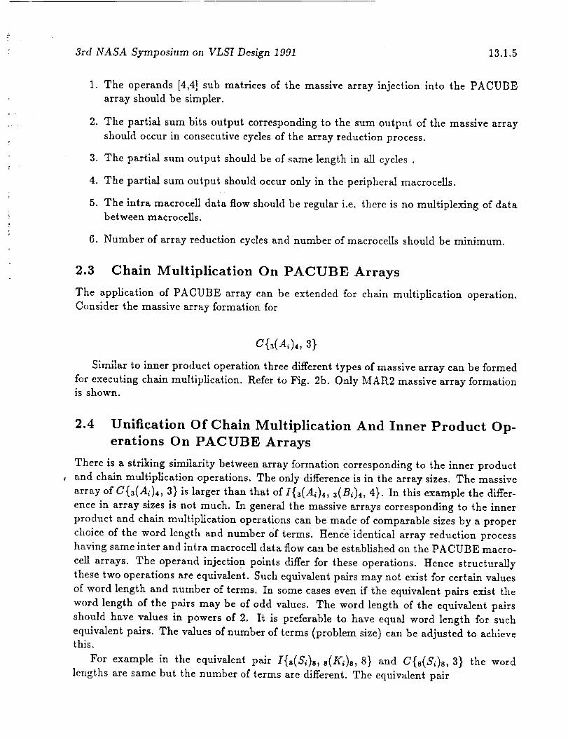
2.3 Chain Multiplication On PACUBE Arrays
The application of PACUBE array can be extended for chain multiplication operation.
Consider the massive array formation for
C(3(A,),, 3}
Similar to inner product operation three different types of massive array can be formed
for executing chain multiplication. Refer to Fig. 2b. Only MAR2 massive array formationis shown.
2.4 Unification Of Chain Multiplication And Inner Product Op-
erations On PACUBE Arrays
There is a striking similarity between array formation corresponding to the inner product
and chain multiplication operations. The only difference is in the array sizes. The massive
array of C{3(Ai)4, 3} is larger than that of I{3(Ai)4, 3(Bi)4, 4}. In this example the differ-
ence in array sizes is not much. In general the massive arrays corresponding to the inner
product and chain multiplication operations can be made of comparable sizes by a proper
choice of the word length and number Of terms. Hence identical array reduction process
having same inter and intra macrocell data flow can be established on the PACUBE macro-
cell arrays. The operand injection points differ for these operations. Hence structurally
these two operations are equivalent. Such equivalent pairs may not exist for certain values
of word length and number of terms. In some cases even if the equivalent pairs exist the
word length of the pairs may be of odd values. The word length of the equivalent pairs
should have values in powers of 2. It is preferable to have equal word length for such
equivalent pairs. The values of number of terms (problem size) can be adjusted to achievethis.
For example in the equivalent pair I{s(Si)s, s(Ki)s, 8} and C{s(Si)s, 3} the word
lengths are same but the number of terms are different. The equivalent pair

l,b+c I a)b+c _ llbq¢ I
_+blc!
_+bzt I ttbl¢ _
I+_$¢ I ,I_j_IG I llb+C I
l+b+c+ a+b+c I ll_+C I llb+¢ I
14b+% t,jbuc 3
a_blc I ,3bi¢_ Izblc3
as_I+, l)btc+ Lib+c +
+Is+++ + _bec+ Izbl¢¢ l+bmc+
l_b+c I a)b_c I llb_¢, Itb_c s
(_) O0
k4blc I ILibt¢ _ ilblc I itbl¢ t I+5 t
%b_0,%_c,l,b,c. .._. %b+
II_IC I II++¢ + llbtC+ ¢441
llb+Cl 'IblCl ¢441 ¢)+t
+,b,+. c+_ %t,i c,d+ ¢)d+ Cld 4
&l_iC| ll_iC ]
I+_1¢ I l+r I
#+fl llrl
e+( s e_f, ezf *
llblC4
gs_l
l+h_ fib _ gl_+
c (+(si_+,+)
_lb)
cs4 scl+, csd I
Cl4_ ¢14s
ctd+
eJ_ lI[s +tfl e f_
t)f I e_f_ el( _
elf ! elf l
Ill +
g_h,
I (3 ($i)4, 3t gil4 ,4)
N_ERIC I_LGOR!TI-Ir'IMAPPING CONCEPT(,-)
, GIPOP
i T,_-- PIIOCIC_R
fl --4 -+ fZ ' +'t+!
IP m_W _ 4-- J---- l_ llI,O('](_ I
I , i ;
'i i 'II
Figure 2: MAR process-2 array formation
I{te(S+)te, tB(Ki)tB, 4}, C{te(St)ts, s(S+)s, s(S3)s, 3} has different word length and prob-
lem size. But C{,s(S,),+, ,s(S+)te, ,e(Sz),s, 3} can be easily decomposed (by proper word
length and term/problem size partitioning)in terms of C{,_(S_)_s, s(S_)s, 8(Sz)s, 3}. That
is C{_a(Si),_, Tt} can be decomposed to/{16(Sl)z_, t_(Ki),_, 4}. Further details on this is
dealt in section 3.3.
This leads to a unified PACUBE VLSI array for executing Inner product and Chain
multiplication operations. Outer product operation and high speed multiplicative division
algorithm [3] are based on chain multiplication operation. Hence the execution processes
of GIPOP functions can be unified on the PACUBE macrocel] arrays.
2.5 Systolic Mapping Of GIPOP Functions
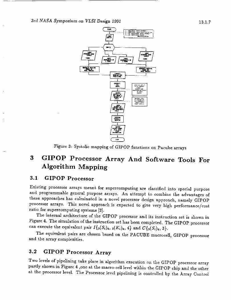
An algorithm has been developed for automatic systolic mapping of GIPOP function ex-
ecution on the P-arrays and implemented under DOS. (Fig 3). The unification of the
execution processes of the GIPOP functions has greatly simplified the development of
systolic mapping tools.
3rd NASA Symposium on VLSI Design 1991
I..,l| OI_F[IIIWT I_.II _ll_l_
e,.,ll (_F_n[bf _Will .
lU_VlTZlC_Vlh
................ _t iro.t?H,czalrl[ mlT_
Figure 3: Systolic mapping of GIPOP functions on Pacube arrays
13.1.7
3 GIPOP Processor Array And Software Tools For
Algorithm Mapping
3.1 GIPOP Processor
Existing processor arrays meant for supercomputing are classified into special purpose
and programmable general purpose arrays. An attempt to combine the advantages of
these approaches has culminated in a novel processor design approach, namely GIPOP
processor arrays. This novel approach is expected to give very high performance/costratio for supercomputing systems [2].
The internal architecture of the GIPOP processor and its instruction set is shown in
Figure 4. The simulation of the instruction set has been completed. The GIPOP processor
can execute the equivalent pair I{a(Si)4, a(K_)4, 4} and C{a(Si)4, 3}.
The equivalent pairs are chosen based on the PACUBE macroceLl, GIPOP processorand the array complexities.
3.2 GIPOP Processor Array
Two levels of pipellning take place in algorithm execution on tile GIPOP processor array
partly shown in Figure 4 ,one at the macro-cell level within the GIPOP chip and the other
at the processor level. The Processor level pipelining is controlled by the Array Control

!3.!,8
°L
SSORY
.................................. 1
_+-LTI R-ULT-II1
_f P,c_E I , + " :1',Re,Ve,SED_ , _ ,,it
h_O£PteI
IPRO_ESSOR F--_,, L
¢ONTROLLE_|: _ j ,ULTrPLIE_J :I
.................... :=:--I-:.......I
GIPOP INSTRUCTION SET
GIPOP PROCESSOR
nRRAY MITH
5M!TCHES
(DC?: o
t_TI_ICTI 014 F0111_T
............... _ ............ _i_iiio_, soURcE,VECTOR'_i_............
[HST_CTIOfl OFEIRANDS , CO_S
; Fipelining of data froa_or_or input port through
I + general purpose registers.
M ; Loads three four-b_t operands
I _ for chain _ultiplicat_on operationeither fro_ _e_or9 or _nput port.
Loads eight four--b_tinner-productop_rands fro_ _e_orv
I or input port,
M Loads eight four-bat_as_[ve arrav operands
I in to the prmarv accumulator.
_ccu_ulate the output o_ GIPOPS_OP ; _n the pri_ar? acc_ulator.
Loads four-Lit _ultiplier fro_M ! _e_orv to scalar _altiplier.
F_¢ ; Loads the _u]tipliqand fr._._beaccumulator _o soa_ar_p_er.
GPR _ Transfer the ouputof g_nera] purpose registers,
. GPOF : GIPOP , primary _ccu_v_a_or ,and the scalar _ultfr_ier
, P_C i _o the output port,(lhese; loa_ings can be done in
MLT ; parallel).
MOU _R,
MOU 6PE ,
MOU CM,
MOU CM,
MOt, IP ,
MOU IP ,
eOU MLT ,
MOU MLT
MOO 0,
MOU 0
_OU 0
MOU 0 ,
=
[I 3( S{)4, 3( K{),, C 3( $1)4, 3( $2 ),_, _($3 ),,, 3 )]
Figure 4: GIPOP processor archuitecture for equivalent pair

3rd NASA Symposium on VLSI Design 1991 13.1.9
Unit (ACU) and the macrocell level pipelining is controlled by the chip control unit (CCU).
The hardware complexity of the switch lattice depends on the processor complexity, data
communication complexity in an algorithm and the word length. The design of the ACU
is under progress.
3.3 Mapping Of Numeric Algorithms On GIPOP Processor Ar-
ray
Mapping of numeric algorithms on the GIPOP processor array involves tackling the com-
putational (levels 1 & 2) and communicational (level 3) complexities.
Level 1. Decomposing the computational structure of the algorithm in terms of
GIPOP equations which are further decomposed in terms of the inner
product functions only [1].
Level 2. The architectural capabilities of a GIPOP processor is bounded by prob-
lem size and worcUength. Suitable algorithms for problem size and word
length partitioning of GIPOP functions and the corresponding software
tools have been developed. The algorithm is based on definitions (3) -
(6) []. Refer to Figure 5.
Level 3. a. Proper loading of input operand frames into the high speed processor
memory (Block level memory loading) from the system memory.b. Programming the processor and array control units.
Numeric algorithm mapping on the GIPOP arrays basically involve mapping of different
inner product blocks (IP Blocks) of variable complexities (see Fig 2c). Functionally each
of these IP Blocks may correspond to different GIPOP operations.The data flow between
the corresponding group of GIPOP processors (making an IP block) can be syntactically
described including both the functional and behavioral aspects of the GIPOP processor
[2] .Mapping of an algorithm on the arrays is to get this syntactical description of the dataflOW.
Software tools for levels 1 and 3 are being developed. The novel concept of mapping
numeric algorithms on the GIPOP processor array shown in Figure 2c greatly simplifies
the development of software tools for levels 1 and 3 above.
4 PACUBE Logic Level
4.1 Inter And Intra Cell Routing.
An efficient algorithm for inter and intra macrocell routing has been developed taking into
account the shortest path considerations. The software tools are shown in Figure 6 asflowcharts.

13.1.10
4.2
f
{ {-'i2 )r
Ap _
I ..:_:-:+:oo].... ---)l _
Mu|ttpl thm
I
Chain Multiplication
I nput ]
1nput/_..... /
[ °'"" 1irerM
partition
[ r;_:*,,_-:o:o]
:J5'es
m WQrdlonrepr_sen+.__ordllngth
Inner Product
Figure 5: Wordlength & term partitioning
Subprogram (Functional Units) Library Generation And Link-
ing.
Several subprograms, Sequential and C0mblnatorial,have beenmapped on tile PACUBE
macrocell. An ei_cient PACUBE Hardware Description Language (PHDL) has been de-
veloped. The subprogram linking is done using this PHDL and the related software tool
has been developed. ( Fig. 7 )
5 PACUBE Circuit Level Discussions
5.1 Interactive Layout Generation And Checking.
A software tool for the generation of device level layouts in an interactive fashion has
been developed (Fig. 8). It provides four layers viz Diffusion, Polysilicon and two levels
of metal. The package supports both n-well and p-well CMOS processes. Lambda based
design rules have been adopted. Special facilities such as mirroring, translation, rotation,
m
L

3rd NASA Symposium or, VLSI Design 1991 13.1.11
+CLOSE (il* _tiabP-_ll ¢*des ]
6
CHAHGE c_lr
Figure 6: Inter-cell logic level tool
step gz repeat , cut _ paste and scaling are available to aid in faster design. The layout of
an entire macrocell has been developed using this tool. Layout geometries are expressed
using PACUBE device level codes. The design rule checker developed is edge based and
performs both inter and intra layer checking.
The different functional units of the macroceU are treated as standard cells and de-
pending on the application the required standard cells can be placed within the maerocell.
This option gives rise to macroceU arrays with different sizes of macroeells.
5.2 Intracell And Intercell Mapping.
A software translator for the PACUBE logic level code to PACUBE device level code
conversion and a device level to Caltech Intermediate Format (CIF) translator has alsobeen developed.

13.1.12
[ .._N ,.1,.' ]i_lrl'_e| I ivif_
C_,ASSJ F¥ l,.,k ,,,+,+4 N¢ I, inll i_4_I, Ii_+.III I ]
i '°
I
II+ ,V I/0
,,_,t: +"+,,ti,tf,,, I
,_A __ _, __
i++.. | yr_
_o+l.Jll. _.l,a+. l,n [I (+r,+,l+.l + +_rld|
L W,,..I.I .... ,l,t,1,1+ It ..... ,I ..... J
I,
l"m,,r'm,+,=u"]
t_
Figure 7: Intra-ceU logic level tool
.3 Simulation ..........5 ........
Circuit simulation of different functional units of t]_e macr0ceH for 1_2 micron tedh-nol-ogy
using PSPICE is nearing completion. Logic level simulation of PACUBE macrocell for
GIPOP operations has been carried out using the PACUBE logic simulator.
6 Conclusion
in this paper novel methodologies have been proposed for designing silicon compilers for
synthesising supercomputing VLSI systems. The important criteria for such a silicon
compiler are integration of its software tools and the architectural considerations.

3rd NASA Symposium on VLSI Design 1991
I -._-.I ]
t
13.1.13
Figure 8: Sub-program linker
7 Future Work
An algorithm for extracting the computational complexities of numeric algorithms in terms
of GIPOP functions is to be taken up. A methodology is to be developed for mapping the
communication graph of numeric algorithms on to the GIPOP processor array as shown in
Figure 2c. Reconfigurable fault-tolerant PACUBE arrays [2] has been developed and the
corresponding software tools to incorporate this into the silicon compiler has to be taken
up.

13.1.14
MnlN PROGRAM •
I sn_cTCHOICEr_ me
p
yo ....... :-,__ ..............I......................( ) o,..,,,o._:STOP I. , 01_1
2 D_I,I
(lncludes Nirroring,
Translation and CutIpaste)
3. S_U[
4 . SORT
5 . HELP
6 . DgL.r_E
7 . $TPI_
8. i_OTATE
9 , E_SE
tO . DIR
11 . $C_LIHG
L.--... ........... . .............. ' .... •
Figure 9: Pacube macro cell based device level layout editor
=

3rd NASA Symposium on VLSI Design 1991 13.1.15
References
[1] N.Venkateswaran, PACUBE Arrays For Supercomputers, Proe. of the Firat Inter-
national Conference on Supercomputing Syatema, conducted by the IEEE Computer
Society and Pentagon, held at Florida, U.S.A., Dec.6-10,1985.
[2] N.Venkateswaran, et al., Supercomputing Systems on PACUBE VLSI Arrays, Re-
search Report. Department of Computer Science and Engineering, Sri Venkateswara
College of Engineering, University of Madras, India.
[3] Joseph J.F.Cavanagh, Digital Computer Arithmetic Design and Implementation, Mc-
Graw Hill publishing house.

m