n s l s -ii b eam lin e d evelop m en t p rop osal · # $ % $ &''!'$ ( !)...
TRANSCRIPT

1 NSLS-II ISR Proposal 2010
NSLS-II Beamline Development Proposal Type I X Type II
A Beamline for Integrated In-situ and Resonant Hard X-ray Studies: Illuminating the Physics of Materials for the 21st Century (ISR) Karl Ludwig (Spokesperson): Prof. of Physics, Boston Univ.; Boston, MA. (617)353-9346. [email protected] Roy Clarke: Prof. of Physics, Univ. of Michigan; Ann Arbor, MI. (734) 764-4466. [email protected] Andrei Fluerasu: Associate Physicist NSLS-II; BNL; Upton, NY. (631)344-4645. [email protected] Randall Headrick: Prof. of Physics, Univ. of Vermont; Burlington, VT. (802)656-0048. [email protected] John Hill: X-ray Scattering Group Leader, BNL-CMPMS Division; Upton, NY. (631)344-3736. [email protected] Jean Jordan-Sweet: Research Staff Member, IBM T.J. Watson Research Center; Yorktown Heights, NY. (631)344-
8581. [email protected] Valery Kiryukhin: Prof. of Physics, Rutgers Univ.; Piscataway, NJ. (732)445-5500 x3899. [email protected] Paul Lyman: Prof. of Physics; Univ. of Wisconsin – Milwaukee; Milwaukee, WI. (414) 229-4626. [email protected] Christie Nelson: Physicist, Brookhaven National Lab, NSLS 725D, Upton, NY. (631)344-4916. [email protected] Ron Pindak: Physical & Chemical Sciences Division Head, NSLS, BNL; Upton, NY; (631)344-7529. [email protected]
A. Science Case We propose an undulator beamline at NSLS-II that utilizes the source’s high brilliance coupled with the latest
advances in x-ray techniques (polarization, resonance, coherence) to create a world-leading, next-generation tender/hard x-ray diffraction facility that addresses key DOE Grand Challenges1:
! How do we characterize and control matter away – especially very far away – from equilibrium? ! How do remarkable properties of matter emerge from complex correlations of the atomic or electronic
constituents and how can we control these properties?” ! How do we design and perfect atom- and energy-efficient synthesis of revolutionary new forms of matter with
tailored properties? As illustrated schematically in Fig. 1 below, addressing these Grand Challenges and making a societal impact requires advances in novel materials using sophisticated investigations with not just a single approach, but rather with a flexible and broad range of capabilities that can be utilized synergistically. To meet this challenge, the ISR Beamline will enable the in-situ study of materials in a flexible range of environment chambers, providing polarization control with a 1 !m vertical focus of the full intensity (nearly 1014 photon/s at 8 keV with Si (111) resolution and nearly 1015 photon/s with multilayers) with 1.5 m working distance from the focusing optic. In addition to facilitating studies of inhomogeneous materials, this will allow the entire beam intensity to be placed at grazing incidence on millimeter-size horizontal samples for surface and interface studies providing a 103 increase over what is currently possible at the leading NSLS beamline X21. For applications needing finer focus, optics for 100 nm vertical spot size will be available. Harnessing developments in coherent x-ray techniques, the ISR Beamline will also enable coherent x-ray photon correlation spectroscopy studies of nanoscale dynamics and complementary imaging studies in complex environments. The energy range of the ISR Beamline (2.1-23 keV) complements and expands the designed energy ranges of the CHX (6-16 keV) and CSX (0.27-1.7 keV) project beamlines at NSLS-II, particularly in its coverage of high interest absorption edges in the tender x-ray regime. The calculated coherent flux B!2/4 of the ISR Beamline at 4 keV is approximately 2x10¹² photons/s with Si(111) resolution.
Also important is our vision of a beamline integrating researchers from university, industry and national laboratory settings to create a community that utilizes detector and computational developments 2 to move sophisticated techniques such as crystal truncation rod (CTR) and x-ray photon correlation spectroscopy (XPCS) analysis into the larger mainstream of the materials research community. With this vision in mind, the ISR Beamline was developed in collaboration with both university and industrial groups as part of a sector that includes a 3PW Materials Physics and Processing (MPP) beamline championed by the IBM group (see Appendix A).
For simplicity, we break the science case into three overlapping directions: 1) the physics of novel materials, 2) atomic structure of functional surfaces/interfaces and 3) growth and materials processes. As one example of their deep interconnection, consider the attraction of growing an ultra-thin oxide film on an oxide substrate while investigating the growth process with real-time x-ray techniques, then determining the atomic structure at the interface with CTR analysis, and finally relating the atomic structure to the electronic structure as measured in-situ with resonant x-ray scattering. Such studies have the potential to significantly increase our understanding of the tunability of orbital, spin, charge and lattice degrees of freedom at the interface between two oxide materials.

2 NSLS-II ISR Proposal 2010
A.1 Physics of Novel Materials New materials, and even new states of matter, are discovered at an accelerating rate. Recent examples include
pnictide high-temperature superconductors, topological insulators, and novel quantum-critical states. From an applied viewpoint, materials combining several functional properties – the multiferroics – hold promise for future device applications. The ISR Beamline will provide a unique tool for studies of these materials. Because of significant resonant enhancement, magnetic signals, multipolar orders, the effects of spin-orbit coupling, charge/orbital order, and the effects of crystalline environment all can be studied in the 3d elements, S and Se chalcogens, and Cl and Br halogens (K-edges); the 4d through the lanthanides and most of the 5d elements (L-edges); and the actinides (M-edges). The combination of such an extended energy range with full polarization control/analysis would be unmatched in the world and will allow definitive characterization of the electronic states, including their multipolar character and the quantum-mechanical nature of the magnetic moment. Importantly, such studies will be possible in environmental chambers with limited access (such as magnets) – a task that requires full polarization control. In another exciting possibility, focused beams as small as 100 nm can be scanned over the sample surface, revealing the nature of the inhomogeneous states and the magnetic domains. This will provide unique insight into the physics of antiferromagnetic domains, chiral magnetic systems, and many multiferroic states, which are inaccessible to other experimental techniques such as PEEM. It will also provide crucial information for future applications of multifunctional materials. Finally, coherent scattering techniques will be used at resonance to study static and dynamic properties of domains in an unmatched range of materials. A.1.1 Resonant X-ray Scattering of Novel Ordered Structures
Interest in 5d materials has exploded recently with discoveries of novel states of matter, including topological insulators3 and quantum spin Hall materials4. The uniqueness of the 5d systems lies in the interplay of the equally strong spin-orbit interaction and the electronic correlations4. It leads to unconventional electronic states that cannot be described using the language of weakly-interacting spin and orbital states. Resonant x-ray scattering (RXS) is a powerful tool to probe these states. In Sr2IrO4, for example, RXS was used to reveal the complex Jeff = 1/2 state of the Ir ion5, and thus a novel spin-orbital Mott state was discovered. This state has been proposed to give rise to a novel topological state of matter and to a quantum Hall effect in hexagonal lattices4, and is also relevant for quantum computing6. A large number of other intriguing 5d compounds are awaiting investigation. Ir systems, in particular, exhibit anomalous magnetic states (Sr3Ir2O7)7, spin-Hall effect (Na2IrO3)4, and unconventional dimerized orbital states (CuIr2S4)8,9. RXS combined with polarization control/analysis can provide definitive insight into the nature of the electronic states of these materials. Large spin-orbit coupling, which is the defining characteristic of the 5d materials, is important for many other fundamental and applied topics. Multiferroic materials10, for example, require large values of this coupling for enhanced magnetoelectric effects, and a search of 5d-based systems (based on Ir-doped Ca3MnCoO6, for instance) is currently underway. From the applied perspective, 5d elements are well known11 to enhance technologically relevant properties (e.g. anisotropy and coercivity) of magnetic recording media and studies of model compounds could lead to advances in this field.
Interest in 4d-based oxides also derives from the wide range of behaviors exhibited by these materials. One class alone, the ruthenates, exhibits ground state phases ranging from the extremely useful (SrRuO3, for use in microelectronic devices due to its good conductivity, surface stability, and resistance to chemical corrosion)12 to the
Develop Materials
with Multi-Functionality
Thermoelectrics
Novel Materials Enhance Devices Addressing Societal Needs in Energy and Information TechnologySolid State Lighting
Fuel Cells
Solar Energy Conversion
Information Processing & Storage
Develop High Functionality Organic Films
Engineer Interfaces for Novel Properties
Nanostructure Growth via Self-
Assembled Processes
In-Situ Atomic Structure of Surfaces & Interfaces CTR, AnomCTR & XRR
Grow Materials with Spin Control
Control Chemical
Reactions at Surfaces
ISR BEAMLINE: Techmiques for Atomic-Level Structural Measurements of Growth and Properties
Top-Down & Bottom-Up Atomic-Level Growth Strategies Used to Produce Novel Device Materials
Electronic, Magnetic & Orbital Structure
RXS, CDI
Time-Resolved Changes duringGrowth & Processes
GISAXS, GID, XPCS, XRIM Pump-Probe Fig. 1
Theory

3 NSLS-II ISR Proposal 2010
exotic (Sr3Ru2O7, which exhibits magnetic field-tuned quantum criticality)13 to the potentially useful and exotic (superconductivity in Sr2RuO4 and the ruthenocuprates). Like the 5d materials, the relevant d states can be probed directly on ISR using L edge RXS.
Many of the most exciting systems in solid-state physics belong to the class of 3d materials. Examples include cuprate and pnictide superconductors, and colossal magnetoresistance (CMR) manganites. Application of RXS at 3d K edges is a powerful technique for analyzing charge- and orbitally-ordered states in these materials14. Recent progress in the field allows the analysis of the electromagnetic multipole nature of the electronic states15, leading to a much improved understanding of the physics involved. This has already led to a reassessment of the nature of several well-known systems, such as an archetypal Mott insulator V2O3, in which the anapole and octupole contributions to the V ground state were established16. These advances clearly show that RXS studies on the K edges of the 3d elements will provide important insight into the physics of these ubiquitous materials. Many of the 3d systems also contain lanthanides, whose magnetism often controls their properties, as in multiferroic REMnO3
17.18. Disentangling the RE and 3d magnetism is crucial for understanding these systems, and RXS makes this separation possible.
Actinide systems exhibit heavy-fermion behavior and exotic multipolar orders19. The latter are responsible for many of the enigmatic “hidden order” phases in heavy fermion materials, e.g. in UPd3
20. Many other hidden order states, such as in U(Ru,Rh)2Si2, are yet to be elucidated. RXS provides a definitive probe of the multipolar orders, and here, again, polarization control/analysis is required.
Most of the materials described above exhibit intriguing magnetic phase diagrams, and studies in a magnetic field are essential. The ISR beamline will combine such studies with full polarization analysis, making it possible, for instance, to do effective "azimuthal" RXS scans in a large magnet. This is an unmatched capability in the US.
With analogous behavior to superconductors21 and helielectric ordering22, systems with liquid crystalline order (LCO) can be described by similar statistical physics concepts as magnetic and correlated electron systems and in fact RXS plays an equally important role here too. In systems with LCO, whether a small molecule, semiconducting oligomer, or biomolecule, the RXS is due to the anisotropic tensor of susceptibility (ATS) that results from orientational ordering of the rigid molecular core23. The ability to readily control the orientational ordering in systems with LCO underlies their technological applications because it provides control of their anisotropic optical, electronic, and mechanical properties. The application of LCO to high-definition flat panel displays is well known, but more recently LCO was also demonstrated to impact the preparation of higher efficiency organic photovoltaic (OPV) devices 24 , 25 . During the last decade RXS was applied to a rich variety of LCO phases with uniaxial screw symmetries where the ATS could be fully determined using linearly polarized x-rays22,26. Microbeam RXS was also successfully applied to measure locally ordered (~100"m) domains in cases where large area alignment was difficult to achieve27. One of the scientific challenges in soft materials for the next decade is to understand LCO in the more-ordered biaxial phases that have the potential for enhanced electro-optical properties, for example by improved overlap of charge transfer complexes. The RXS structural determination of the biaxial phases and their associated biaxial ATS, which can involve glide as well as screw symmetries, will require two enabling features of the ISR Beamline: the availability of both linear and circular polarized x-rays28,29 and access to both the tender x-ray edges of the P, S, Cl atoms found in many soft materials and the hard x-ray Se or Br edges for measurements in device structures under operating conditions30. A.1.2 Electronic and Magnetic Domains – X-ray Imaging
A major theme in the study of strongly correlated electron materials is that there are many possible ground states reflecting different ordering of electronic degrees of freedom, and these states have only small differences in their free energy. In many cases, this leads to electronic phase separation31. Such states are essential for understanding CMR and superconductivity, and could lead to design of new high-response sensors. Typical domain sizes for the different phases can range up to several microns. The separate phases often have little difference in the atomic structure and are primarily characterized by electronic or magnetic ordering, thus they are difficult to measure. This is also true for the general case of non-ferromagnetic domains. RXS allows for exploring this fundamental feature of complex materials. Two possible approaches would be rastering a microbeam over the sample32, and using inversion techniques to obtain real-space images from coherent x-ray scattering data. The first approach is based on “dark-field imaging” of multiple-q states, or on circular and linear dichroism of RXS. It is uniquely sensitive to the nature of the magnetic states, and can reveal chiral and antiferromagnetic domains. The second approach has not yet been demonstrated, but is a current research thrust of JPSI. ISR would be the first diffraction facility with such a capability for magnetic RXS with polarization control in the tender and hard x-ray energy ranges.
Numerous systems can be studied by this technique. Among correlated materials, candidates are novel superconductors, such as oxygenated FeTe films33, in which antiferromagnetic/superconducting phase separation has

4 NSLS-II ISR Proposal 2010
been conjectured. Other examples include hidden (charge?) order in phase separated SrCoO3-y, and stripe domains in La5/3Sr1/3NiO4
34. A whole new topic covers novel magnetic domains in multiferroics, where chiral magnetism, vortex states, and magetoelectric freezing are observed35,36,37. These phenomena attract attention in many fields, ranging from graph theory to information storage and photovoltaic applications. Importantly, these applications depend on (or are limited by) the properties of the multidomain states in the most promising materials, such as BiFeO3 in which domain wall type and density determine the magnitude of the photovoltaic effect38. Understanding microscopic magnetism of these states is crucial for design of future multiferroic devices with enhanced photovoltaic properties and memory density. Scanning diffraction provides an unmatched magnetic probe for these states (positions and, possibly, type of the domain walls, microscopic magnetism in the domains inaccessible to other techniques), which should result in significant advances in controlling the domain states and in device design. A.2 Atomic Structure of Functional Surfaces and Interfaces
Though there is substantial knowledge of the behavior and reactivity of surfaces in UHV environments, many of the most important catalytic and electrochemical processes occur at gas-solid and liquid-solid interfaces. In the case of the gas-solid interface, the current lack of understanding of such interfacial processes is known as “the pressure gap.” It is also increasingly apparent that buried solid-solid interfaces can be engineered to create magnetic and electrical properties which differ fundamentally from those of either constituent material. X-rays offer a unique opportunity to penetrate many complex environments (gas, liquid, or solid thin-film overlayers) to probe the structure and chemistry of surfaces and internal boundaries from macroscopic lengths down to the atomic level. The ISR Beamline will bring unprecedented brilliance and also enable resonant scattering studies that can dramatically improve diffraction phasing. Moreover, the polarization control of the beamline will facilitate the use of existing surface-sensitive x-ray techniques to study magnetic order at interfaces and surfaces.
Because of the difficulty of collecting and interpreting data, these techniques are still the purview of a relatively modest number of synchrotron-focused scientists. However, the rate of data collection and analysis is improving –on-the-fly CTR scans have been demonstrated and there is continuing progress in ab-initio solutions of interface structure from complete CTR sets. Coupling the brilliance of the ISR Beamline with fast area detectors and advanced software, we envision the technique evolving into a tool capable of making routine measurements of the full, 3-d structure of complex systems and moving toward the mainstream of materials researchers. A.2.1 Gas-Solid and Liquid-Solid Interfaces
Surface-dominated phenomena span a range of disciplines, and surface/interface x-ray diffraction has already shown that it can make seminal contributions. In geochemistry, the fluid-solid interface can be probed to understand structure and relaxation of the mineral39, the reaction of the mineral with water40, the adsorption of dilute species (~ML quantities)41, and the speciation of water near the crystal surface42. From the point of view of fundamental studies of condensed matter, the (partial) ordering of liquids near the interface with a gas43 or with solid walls44,45,46,47 can be observed by x-ray studies, and many open questions remain. Another fundamental problem in condensed matter accessible to x-ray scattering is the stable arrangement of the surfaces of polar oxides; these materials, due to a non-vanishing bulk dipole moment normal to the surface, have an inherently high surface energy48, but may lower this energy by forming an air-stable reconstruction49,50,51,52,53 or by adsorbing materials from the ambient54. In some cases, the reconstruction is stable even under a bulk water layer55. Deposition of macroscopic amounts of material from solution (i.e., crystal growth) can be monitored using surface x-ray diffraction56. The field of electrochemistry, although dating back hundreds of years, has been revolutionized by the ability of x-rays to penetrate the active medium and directly observe structures57 and reactions58 at the interface. In particular, x-ray scattering can probe the structure of the electrical double-layer not only in an electrochemical cell59, but also with applications in the fields of geochemistry60 and biology61. Investigations of catalysis using x-ray diffraction under real-world conditions give atomic-scale insight to important catalytic reaction mechanisms62. Indeed, better understanding and controlling electrochemical interfaces is key to several developing energy technologies. As one example, solid oxide fuel cell (SOFC’s) is currently limited by the oxygen reduction reaction at the cathode, but little is known of the atomic details of this process. The community is only beginning to investigate issues of surface segregation and termination layer as a function of pO2, temperature and electric potential. In typical SOFC structures, the dominant reaction area for oxygen is near triple phase boundaries (TPB) between the gas, the electron-conducting cathode and the ion-conducting solid electrolyte. With its 1 !m focused beam, ISR offers opportunities to investigate atomic-level structure and composition near the TPB’s of patterned samples. Related interface issues occur in the development of oxide gas sensors, nitrides for H2 production by solar powered photolysis, and proton exchange membrane fuel cells.
5 NSLS-II ISR Proposal 2010
Due to weak scattering signals, surface and interface magnetism has been difficult, but not impossible63, to probe using a synchrotron x-ray source, and recently has found an increasing number of applications64. The polarized and tunable source envisioned for the ISR will greatly facilitate studies of interfacial and surface magnetism. In addition to these established fields, a host of potential applications arise in studying, for example, organic-inorganic interfaces important for solid-state lighting65, the “top-down” nanopatterning using dip-pen lithography66, or interface reactions found in batteries and supercapacitors67. A.2.2 Engineered Solid-Solid Interfaces for New Materials Properties
The physics of hetero-interfaces is an exciting new field of research that has witnessed a number of breakthroughs in the last few years. The recent discoveries include interface superconductivity68, interface magnetism69, high-mobility two-dimensional electron gas 70 , colossal ionic conductivity 71 , and colossal magnetoresistance 72 . The importance of these developments lays in the fact that nearly all current electronic and optoelectronic materials applications and devices rely on heteroepitaxial interfaces, including compound semiconductor heterostructures and oxides exhibiting correlated-electron behavior. As many of these novel properties are strongly dependent on stoichiometry and finite size effects, strict control over film composition and thickness is essential. Deposition methods as molecular beam epitaxy (MBE) and pulsed laser deposition (PLD) achieve reasonable stoichiometric and excellent thickness control. Growth takes place far from equilibrium, however, implying that the kinetics of deposition heavily influence the resulting structure and electronic properties. Moreover, the many possible structural configurations may differ in energy by only a few tens of milli-electronvolts per atom, which is several orders of magnitude smaller than the cohesion energy. For these reasons, the structure of the buried interfaces is difficult to predict theoretically from first principles. The ISR Beamline's instrumentation to precisely measure CTRs as a function of energy (Anomalous CTR) will provide knowledge of the atomistic (chemical and crystallographic) structure of the buried hetero-interfaces73,74, which will enable theorists to better understand and predict the emergent physics and enable film growers to refine their growth processes.
Equally interesting and technologically relevant are the interfaces and internal structure of quantum dots (QDs). QDs have applications in optoelectronic devices75, quantum information processing76, and energy harvesting77. Using the CTR technique, the structure of electronic QDs was recently shown to reveal a number of surprises including exchange of the QD material with the substrate as well as a complex internal QD structure78. Particularly interesting are recently discovered core-shell structures which offer the possibility to tailor-make QDs with desirable optoelectronic properties. The polarization control of ISR will enable the extension of the CTR technique to measure atomic-scale variations in magnetic thin films as well as magnetic QDs, which are of interest for spintronic devices79. A.3 Time-Resolved Studies of Growth and Materials Processes
There is a vital need to improve our basic understanding of dynamic processes in materials, ranging from growth processes controlling material properties at the nanometer or atomic level, to fundamental interactions between lattice and electron degrees of freedom. The high brilliance of the ISR Beamline will enable important advances, beginning with the increased time resolution possible with existing “incoherent” surface-sensitive x-ray techniques since the entire flux of the beam can be placed on millimeter-size horizontal samples at grazing incidence. Beyond this, the NSLS-II undulator source will also give an enabling impetus to the development of surface-sensitive coherent x-ray fluctuation spectroscopy studies of surface dynamics which are currently in their infancy. XPCS studies of CTRs, specular reflectivity and Kiessig fringes will provide unique information about nanoscale surface dynamics80.
Emerging imaging techniques for surface and interface structures will also receive a major impetus from the NSLS-II. Details of many phenomena such as island formation are not readily available without direct, real-space observation. X-ray Reflection Imaging Microscopy (XRIM) is a very promising new technique that exploits phase contrast from steps or buried interfaces to allow imaging from buried boundary structures with spatial resolution approaching 30 nm in-plane and with angstrom-scale step sensitivity81.
Beyond the x-ray capabilities, the flexibility of the ISR Beamline will enable the complementary in-situ studies, e.g. laser measurement of thin film stress evolution, that often need to be correlated with the x-ray results to develop a complete picture of the relevant physical processes. A.3.1 Fundamental Processes during Film Growth
The details of the physical processes occurring during growth often remain poorly understood, partly because of the many relevant time-scales (Fig. 2). PLD, which is perhaps the pre-eminent method for growth of complex oxide materials including ferromagnetic/antiferromagnetic layers, ferroelectrics, and multiferroics, uniquely provides direct access to the microsecond time scales of adatom addition and diffusion because of the time structure of the deposition itself. Significant work is needed to understand fundamental mechanisms of processes such as fast interlayer transport at microsecond time scales82,83. A wide variety of other issues remain to be resolved including the role of strain in

6 NSLS-II ISR Proposal 2010
modifying properties such as ferroelectric polarization, the role of interfaces in modifying properties of multilayers, the relationship between geometric structure, chemical bonding, and electronic structure at surfaces and interfaces.
Growth of oxide materials by sputter deposition occurs in a significantly different kinetic regime than in PLD but, when an off-axis geometry is used, high quality epitaxial thin films and superlattices can be made for substantially lower cost. Ultra-thin ferroelectric thin films of interest for applications ranging from non-volatile computer memories to advanced micro electro-mechanical actuators and sensors provide a specific example of the problems that need to be investigated. These materials are highly sensitive to external boundary conditions and also have a very strong coupling between structure and electrical polarization, making x-ray diffraction the ideal tool to study them. During growth both the crystalline structure and domains within the material change in complex ways on a relatively short time scale, which can in practice only be accessed with the intensity of a next generation synchrotron source. These changes continue upon post deposition cooling and change once again when the sample is exposed to the atmosphere. Only by monitoring these changes throughout the growth and cooling will we be able to take full advantage of the opportunity to drive the materials towards a particular set of properties by control of the growth process.
As another example of the growth science enabled by ISR, consider that a complete understanding of the fundamental mechanisms governing the evolution of film stress, roughness, and interface mixing in sputter deposited layers has not been achieved despite the technique’s widespread commercial use since the 1970’s. While real-time studies can examine the evolution of the roughness power spectrum during deposition the “incoherent” GISAXS pattern stops evolving when the roughness spectrum reaches a steady state. However, with the brilliance of the NSLS-II source, XPCS in the GISAXS regime will provide unique information about the dynamics of the surface roughness as sputter deposition continues.
In these examples adatoms join crystal lattices directly from the vapor, but in InN, GaN and their related alloys, a thin mobile layer forms on the surface during successful growth, promoting diffusion of adatoms to step edges. Thus the deposition may have characteristics of liquid phase epitaxial growth. This may be related to atomic ordering and/or phase separation observed in the ternary alloys84. The high time and spatial resolution of the ISR Beamline will allow the overlayer structure and chemical composition to be probed locally to investigate these phenomena.
An important range of growth techniques utilize surface reactions for the growth process. Of these, Atomic Layer Deposition (ALD) is of great importance for its high conformality and ability to control growth layer by layer. Recent real-time x-ray studies of ALD growth kinetics at NSLS X21 are, to our knowledge, the first of their kind85. Because of the low intensity from single monolayers, however, current experiments need to integrate over many seconds to observe changes associated with growth from individual gas cycles. The high brightness of the ISR beamline will enable significantly deeper investigations addressing at least two key issues: 1) What is the growth kinetics within a
single gas pulse and when is saturation achieved? 2) For ALD of metals, often no observed growth during the first couple of cycles, but it is known that the surface is evolving – what is happening and how does it relate to the eventual film nucleation? A.3.2 Growth of Electronic and Optoelectronic Organic Materials
Comparatively speaking, studies of organic thin film growth are in their infancy86. Yet, there are many key questions in organic film growth to be addressed in order to optimally control the structure of films and interfaces for applications such as organic photovoltaics (OPVs), light-emitting diodes, and organic field-effect transistor. In-situ time resolved studies will yield important information about the formation of organic-inorganic interfaces. For example, in-diffusion of aluminum or other metal into the active layer of the devices such as OPVs will have a significant effect on the performance of devices. While processes
Fig. 2: Time-scales and wave-numbers of thin film growth processes accessible to ISR within experimental limitations.

7 NSLS-II ISR Proposal 2010
such as deposition of metal contacts utilize vacuum deposition, other processes are carried out in ambient environments. In particular, studies of deposition of films from liquid solutions require customized deposition stages, nozzles, or other instruments to study processes such as roll-to-roll deposition onto polymer surfaces. Many questions related to the kinetics of crystallization and ordering during drying from liquid solutions can be addressed through techniques such as in-situ GISAXS and x-ray reflectivity. These studies will have a profound impact on our understanding of real-world industrial processes. A.3.3 Growth of Self-Organized Nanostructures
Self-organized nanoscale structuring is an important paradigm for the formation of new functional materials with relatively low cost. Perhaps the mechanism most widely used today is semiconductor QD formation due to Stranski-Krastanov growth. Even here, however, many questions remain about the evolution of nanodot morphology and the interface between the dots and the substrate. Moreover, due to limitations of the Stranski-Krastanov approach, there is increasing interest in using droplet epitaxy, in which liquid nanodroplets on the substrates are used as reactants or solvents for subsequent growth. In some cases, such as plasma nitridation of Ga or In droplets, nanodots are formed87. In others, such as the growth of vertical nitride nanowires, a droplet of another material (e.g. Au) can act as a solvent and catalyst for the growth process88. Such semiconductor nanowires have the potential to improve the efficiency of energy-relevant devices from photovoltaics and solid-state lighting, to high-power, high-temperature electronics. In all of these cases, the high brilliance of ISR will enable study of nanostructure nucleation, and the evolution of shape, chemical composition and strain during growth – giving insight into the mechanisms driving nanoscale self-assembly. A.3.4 Phase Transformations during Rapid Thermal Annealing (RTA)
As microelectronics devices shrink, and new materials and processes are incorporated to improve performance, the behavior of interfaces and reduced dimensions have an increasingly major effect. The brilliance of the proposed ISR beamline will enable the investigation of ultra-thin films and features with high resolution in reciprocal space at the necessary time scales associated with the evolution of key material properties. Real-time diffraction, in conjunction with complementary measurements such as optical light scattering, yields vital information about the behavior of thin films and small features during processing. Crystallographic phase formation, grain orientation and size, interfacial and surface roughness, strain, and transition temperatures can all be measured during rapid thermal or laser annealing. Materials of interest to the microelectronics industry include copper for interconnects89, metal silicides for device contacts90 , lead-free solders91 , phase change materials for advanced memory92 , ultra-low-k dielectrics for insulation of the transistor gate93, and diffusion barriers between copper and silicon or dielectrics94. While thin films are studied for preliminary assessment of process and materials parameters, arrays of nanopatterned features can be measured to determine the effect of physical scaling. Often nucleation or diffusion effects will change the kinetics of phase formation in small features95. While some of these systems could be measured during rapid thermal annealing on the proposed MPP Beamline, there are cases where the high brilliance of the ISR Beamline will be needed. Examples are samples whose diffraction peaks cannot be resolved, such as films that undergo cubic-to-tetragonal phase transformations; dilute structure arrays or thin films that need higher intensity; and small single features that need a smaller spot size. In addition, faster annealing rates or even laser annealing could be used on the ISR Beamline, and anomalous diffraction at absorption edges not available at MPP could be used to discern complicated structures. Complementary measurements with a nanometer-scale x-ray probe are also of interest. Looking at an isolated feature while current is running through it allows investigation of electromigration.
The ISR beamline provides a unique combination of tools to interrogate the behavior of materials and structures for microelectronics technologies in the longer-term future as well. For example, coherent Bragg rod analysis of crystalline nanowires will enable the investigation of strain distributions96, which have a large impact on carrier mobility due to piezoresistance, within the nanowires. By exposing them to a variety of ambients and temperatures, the evolution of strain that can be induced by oxidation of the nanowires can be monitored in-situ.
The scaling of device dimensions has resulted in gate insulators composed of silicon dioxide to exhibit significant leakage and eventual breakdown between the gate and channel at their target thickness. By incorporating complex oxide films that possess higher dielectric constants, leakage current can be mitigated while maintaining equivalent oxide thicknesses of 2 nm and below. However, subsequent manufacturing procedures may alter the microstructure of the high-k dielectric films from their desired amorphous state. X-ray studies of these films during in-situ annealing will help elucidate the parameters controlling crystallization and phase separation within candidate materials97,98. A.3.5 Kinetics of Thermal and Spin Processes
NSLS-II offers a single-bunch timing structure that is usefully short (~30 psec) compared to that of existing storage-ring sources (e.g., 70 -100 psec at APS). This presents an opportunity for ISR: i.e. drawing on Proposal Team expertise to extend its time-resolved capability into the intermediate temporal regime of relevance to the dynamics of

8 NSLS-II ISR Proposal 2010
thermal transport and spin wave propagation and relaxation. These techniques are based on the pump-probe approach. This 30 psec and longer time scale enables studies of a wide range of excitations including coherent acoustic phonons and spin waves, and covers the range from electron cooling and optical phonon relaxation all the way through to thermal transport and lattice cooling; it is a very different regime than, and does not compete with, that of ultra-fast FEL or slicing techniques. Moreover, it is expected that in the next five years reliable fiber lasers will make laser operation in this regime more routine. Many of the studies envisioned will take advantage of the special characteristics of ISR, especially the polarization capabilities (e.g. to study effects of magnetic anisotropy on magnetic switching), and the tunability which will enable magnetic dichroism experiments to be performed near specific edges.
An example at the latter end of this temporal spectrum is the relaxation of long-lived spin wave excitations, relevant to the magnetic perovskite systems (LaSrMnO3). It would be very interesting, for example, to insert thin layers of LSMO into an ultrathin ferroelectric film, to study spin-injection effects and magneto-elastic interactions. This novel multiferroic heterostructure is made feasible by functional interfacial layers that can be made by oxide heteroepitaxy, for example using pulsed laser deposition. The central physics to be studied here is the basic nature of ferroic coupling and how it can be manipulated optically. This is ideally done in the time domain where the coupled spin and phonon excitations can be distinguished on account of their very different relaxation rates.
The same time-resolved x-ray techniques can be employed for analogous studies in molecular crystals and polymeric systems that exhibit structural rearrangements associated with electronic or magnetic relaxation processes, e.g. lattice relaxation associated with excitons, which is relevant to organic photovoltaics. Of particular interest are collective dynamical phenomena that take place in the hundreds of picoseconds time span following light excitation. Also, magnetic dichroism can be used to study spin relaxation in organic crystals with structures containing Mn, Fe or Co, which have been found to exhibit ferro- or paramagnetism99,100. Unlike their inorganic counterparts, a change in the spin state of the magnetic ion that is photo-induced using visible light can be accompanied by a change in the local structure 101 , which opens the possibility of directly correlating magnetic and structural information through complementary techniques such x-ray magnetic dichroism and time-resolved diffraction.
B. Beamline Concept & Feasibility The ISR Beamline will use versatile optics taking advantage of the source’s high brilliance and at a given time
feed either of two stations, each with unique capabilities. The beamline layout allows experiments to be performed in the upstream hutch (Endstation-A) while sophisticated growth/processing studies using larger chambers are prepared for upcoming beamtime in the downstream hutch (Endstation-B). This will considerably increase productivity. In order to achieve the necessary focusing resolution, ISR will need to be located an area with extended floor space. B.1 Source
The undulator design will be chosen to maximize coverage of the 2.1-23 keV energy range while minimizing source size and beam divergence. The lower limit is determined by the choice of Si(111) as a standard monochromator, while the upper limit is determined by the undulator sources being considered. The energy range will cover K edges from phosphorus through the 3d transition metals and up through ruthenium, and L edges of the 4d and 5d transition metals, as well as the rare earths. A high-beta straight is desired to minimize beam divergence, and the 3m IVU20 design works well, though with a gap between the first and third undulator harmonics at ~ 4 - 4.9 keV. The missing energy range does not include any absorption edges of high current interest. Another advantage of using a 3m undulator is that it would leave room for a canted partner for future buildout (see Appendix B). B.2 Upstream Optics
Separate dynamically bent horizontal and vertical mirrors will be used to focus the full beam to a secondary source point (Fig. 4). The use of the secondary source enhances beam stability and allows great flexibility to change the source’s effective size, which is particularly useful in controlling the number of coherent modes in the incident beam. Typical parameters from calculations suggest a secondary source size of 10 x 200 !m (VxH) FWHM with vertical and horizontal beam divergences of approximately 24 !rad. The quality of the figure on the mirrors is important – they should at least conform to current standard of < 300 nrad slope error, though < 100 nrad slope error would be desirable to better preserve the beam brilliance.
A double-crystal monochoromator will be used, capable of covering the full range 2.1-23 keV with Si(111) resolution of "E/E = 1.5 x 10⁻⁴. Over a reasonable part of that energy range, the monochromator should also support higher energy resolution (e.g. Si (311)) crystals for increased longitudinal coherence in wide-angle coherent experiments as well as multilayers for high-flux experiments using the full spectral width of the harmonic. Due to the power density on the first monochromator crystal, it will be cryogenically cooled. It is vital, however, that this be done without causing vibrations in the crystal which would destroy the time-averaged beam coherence.
9 NSLS-II ISR Proposal 2010
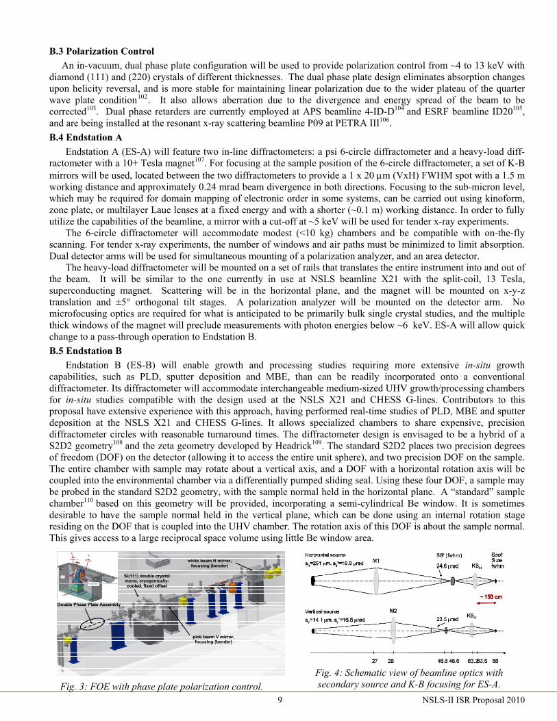
B.3 Polarization Control An in-vacuum, dual phase plate configuration will be used to provide polarization control from ~4 to 13 keV with
diamond (111) and (220) crystals of different thicknesses. The dual phase plate design eliminates absorption changes upon helicity reversal, and is more stable for maintaining linear polarization due to the wider plateau of the quarter wave plate condition102. It also allows aberration due to the divergence and energy spread of the beam to be corrected103. Dual phase retarders are currently employed at APS beamline 4-ID-D104 and ESRF beamline ID20105, and are being installed at the resonant x-ray scattering beamline P09 at PETRA III106. B.4 Endstation A
Endstation A (ES-A) will feature two in-line diffractometers: a psi 6-circle diffractometer and a heavy-load diff-ractometer with a 10+ Tesla magnet107. For focusing at the sample position of the 6-circle diffractometer, a set of K-B mirrors will be used, located between the two diffractometers to provide a 1 x 20 "m (VxH) FWHM spot with a 1.5 m working distance and approximately 0.24 mrad beam divergence in both directions. Focusing to the sub-micron level, which may be required for domain mapping of electronic order in some systems, can be carried out using kinoform, zone plate, or multilayer Laue lenses at a fixed energy and with a shorter (~0.1 m) working distance. In order to fully utilize the capabilities of the beamline, a mirror with a cut-off at ~5 keV will be used for tender x-ray experiments.
The 6-circle diffractometer will accommodate modest (<10 kg) chambers and be compatible with on-the-fly scanning. For tender x-ray experiments, the number of windows and air paths must be minimized to limit absorption. Dual detector arms will be used for simultaneous mounting of a polarization analyzer, and an area detector.
The heavy-load diffractometer will be mounted on a set of rails that translates the entire instrument into and out of the beam. It will be similar to the one currently in use at NSLS beamline X21 with the split-coil, 13 Tesla, superconducting magnet. Scattering will be in the horizontal plane, and the magnet will be mounted on x-y-z translation and ±5° orthogonal tilt stages. A polarization analyzer will be mounted on the detector arm. No microfocusing optics are required for what is anticipated to be primarily bulk single crystal studies, and the multiple thick windows of the magnet will preclude measurements with photon energies below ~6 keV. ES-A will allow quick change to a pass-through operation to Endstation B. B.5 Endstation B
Endstation B (ES-B) will enable growth and processing studies requiring more extensive in-situ growth capabilities, such as PLD, sputter deposition and MBE, than can be readily incorporated onto a conventional diffractometer. Its diffractometer will accommodate interchangeable medium-sized UHV growth/processing chambers for in-situ studies compatible with the design used at the NSLS X21 and CHESS G-lines. Contributors to this proposal have extensive experience with this approach, having performed real-time studies of PLD, MBE and sputter deposition at the NSLS X21 and CHESS G-lines. It allows specialized chambers to share expensive, precision diffractometer circles with reasonable turnaround times. The diffractometer design is envisaged to be a hybrid of a S2D2 geometry108 and the zeta geometry developed by Headrick109. The standard S2D2 places two precision degrees of freedom (DOF) on the detector (allowing it to access the entire unit sphere), and two precision DOF on the sample. The entire chamber with sample may rotate about a vertical axis, and a DOF with a horizontal rotation axis will be coupled into the environmental chamber via a differentially pumped sliding seal. Using these four DOF, a sample may be probed in the standard S2D2 geometry, with the sample normal held in the horizontal plane. A “standard” sample chamber110 based on this geometry will be provided, incorporating a semi-cylindrical Be window. It is sometimes desirable to have the sample normal held in the vertical plane, which can be done using an internal rotation stage residing on the DOF that is coupled into the UHV chamber. The rotation axis of this DOF is about the sample normal. This gives access to a large reciprocal space volume using little Be window area.
Fig. 3: FOE with phase plate polarization control.
Double Phase Plate Assembly
Si(111) double crystal mono, cryogenically-cooled, fixed offset
pink beam V mirror, focusing (bender)
white beam H mirror, focusing (bender)
Double Phase Plate Assembly
Si(111) double crystal mono, cryogenically-cooled, fixed offset
pink beam V mirror, focusing (bender)
white beam H mirror, focusing (bender)
Fig. 4: Schematic view of beamline optics with secondary source and K-B focusing for ES-A.

10 NSLS-II ISR Proposal 2010
Dual arms will be provided for simultaneous GISAXS and wide-angle scattering. The flexible diffractometer geometry enables both hard x-ray diffraction with significant air paths, and tender x-ray studies with thin windows and minimal air path. Incident beam K-B mirrors will provide vertical spot sizes down to 1!m. The system will be designed to minimize vibrations and will incorporate features that optimize use with surface preparation equipment111. B.6 Infrastructure
The area adjacent to Endstations A and B will be used for the experiment control area. For studies of growth and other processes utilizing roll-on chambers, it is vital for such space to be near the hutches. This should include the same support facilities that the hutches provide, including gas handling, gas cabinet, ventilation, and laser support.
C. Required Technical Advances Diamond Phase Retarders – Commercially-available diamond is too thick to work well below 4 keV, so R&D is
required to develop phase plates of other low-Z materials. This effort is now underway at NSLS (Nelson). Precision Positioning in Chambers — Sample stages that incorporate active optical feedback control of sample
position and orientation need to be developed to compensate for thermal drift and thereby make efficient use of micron-scale beams for studies above (e.g. ~ 800°C film growth) or below room temperature.
Mechanically Stable Double-Crystal Monochromator - the large energy range featured by the ISR Beamline requires the use of a double-crystal monochromator; the mechanical engineering design of the monochromator will need to be carefully evaluated in order to not degrade the coherence properties of the x-ray beam.
D. User Community and Demands There will be a large local and global demand for access to ISR due to the increasing importance of addressing the
relevant materials issues for societal needs. Locally, there have been at least 11 workshops on related science at NSLS/CFN Annual Users’ Meetings and other BNL meetings in the past 5 years (see Appendix D) and current users of the diffraction beamlines X14A, X20A, X20C, X21 and X22C (a combined total averaging 157 per year) are likely to be interested in the new opportunities at ISR. Indeed, with the capabilities offered by ISR which have no analog at the NSLS facility (e.g. coherent techniques, tender x-ray scattering, CTR-capable diffractometers, hard x-ray polarization control, tender/hard x-ray pump probe), demand will increase significantly even within the current NSLS user community. Meanwhile, the attributes of ISR that are unique in the world will attract new users from a surface community which is large and growing. For example, at the Advanced Photon Source (APS), the interface science community now involves 11 beamlines, though none match the capabilities of the proposed ISR Beamline. Meanwhile, for APS beamlines serving a user community focused on correlated electron systems (4-ID-D and 6-ID-B,C), data show that over the past 3 years, the subscription rates have been ~ 300-350%, with ~ 170 unique users112.
E. Proposal Team Expertise and Experience Karl Ludwig – Spokesperson (Professor of Physics – Boston University) has nearly 30 years of synchrotron
experience. His work uses real-time experiments to study growth processes and XPCS to examine dynamics. Roy Clarke (Professor of Physics - Univ. of Michigan) has over 30 years synchrotron experience and co-founded an
APS sector for time-resolved studies. He uses direct methods to study QD and buried oxide interface structure. Andrei Fluerasu (Associate Physicist, NSLS-II) has more than 10 years of synchrotron experience and is group
leader of the NSLS-II coherent hard X-ray beamline. He developed microfluidic-XPCS. Randall Headrick (Associate Professor of Physics – Univ. of Vermont) has 20 years of synchrotron experience. He
developed several innovations for real-time studies of film growth and surface dynamics. John Hill (Physicist- Condensed Matter Physics and Material Science, BNL), is group leader of the BNL X-ray
Scattering Group with over 20 years synchrotron experience, particularly using resonant techniques. Jean Jordan-Sweet (Research Staff Member - IBM T.J. Watson Research Center) has over 26 years experience as a
beamline scientist; she is spokesperson for X20 and helped develop !diffraction there. Valery Kiryukhin (Associate Professor of Physics - Rutgers University) has more than 15 years of synchrotron
experience including resonant scattering and scattering in high magnetic fields. Paul Lyman (Professor of Physics; University of Wisconsin-Milwaukee) has nearly 15 years of synchrotron
experience. His research examines atomic structure of surfaces with new approaches for CTR study. Christie Nelson (Physicist – NSLS) has more than 17 years of synchrotron experience and is the spokesperson for the
X21, X16B and X22A beamlines. Her recent focus has been multiferroic materials. Ron Pindak (Chemical and Physical Sciences Division Head – NSLS) has over 30 years synchrotron experience and
co-pioneered synchrotron studies of 2D physics and resonant scattering in LCs and CTR phase retrieval.

11 NSLS-II ISR Proposal 2010
F. Suggestions for BAT Membership
Suggested BAT members are the members of the Proposal Team (R. Clarke, A. Fluerasu, R. Headrick, J. Hill, J. Jordan-Sweet, V. Kiryukhin, K. Ludwig, P. Lyman, C. Nelson, R. Pindak) and:
Ken Evans-Lutterodt: Physicist, NSLS, BNL; Upton, NY. (631)344-2095. [email protected]
Jonathan Lang: Advanced Photon Source, ANL; Argonne, IL. (630)252-0122. [email protected]
Phil Willmott: Professor, Swiss Light Source, PSI; Villingen, Switzerland. +41 (0)56 310 51 26. [email protected]
Oleg Shpyrko: Asst. Professor of Physics, UC-San Diego; San Diego, CA. (858)534-3066. [email protected]
J"rg Strempfer: HASYLAB, DESY; Hamburg, Germany. +49 40 8998-4855. [email protected]
Paul Zschack: Advanced Photon Source, ANL; Argonne, IL. (630)252-0860. [email protected]

12 NSLS-II ISR Proposal 2010
Appendix A – Coordinating Materials Physics and Processing (MPP) Beamline
Jean Jordan-Sweet is leading a Team proposing a 3PW Beamline for Materials Physics and Processing (MPP) that will focus on 1) real-time, in-situ studies of phase transformations of thin blanket films, stacks, and nanopatterned samples, and 2) x-ray diffraction and scattering techniques on solids, including thin films, stacks, nanopatterned samples, and bulk materials; with the capability for mounting small environmental chambers, bending jigs, and displexes. It would form a natural partner to the ISR program intellectually, and in practical use of the neighboring floor space (see layout below).
The Proposal Team for the MPP beamline is: Jean Jordan-Sweet (Research Staff Member, IBM T.J. Watson Research Center) Valery Kiryukhin (Professor of Physics, Rutgers University) Christian Lavoie: (Research Staff Member, IBM T.J. Watson Research Center), Yorktown Heights, NY. Conal Murray (Research Staff Member, IBM T.J. Watson Research Center) Christie Nelson (Physicist, NSLS) I. Cevdet Noyan (Professor of Applied Physics, Columbia University)
If the MPP and ISR beamlines were not constructed, the impact on NSLS-II would be significant: 1. NSLS-II would not be able to provide researchers with the capability of providing atomic-level structural
information including magnetization and chemical composition of buried interfaces, which is critical information to develop a first principles understanding of the emergent new physical phenomena that occur at interfaces. BNL and Stony Brook University would, hence, not be able to take full advantage of their investments in atomic level growth facilities such as those developed by Ivan Bozovic (MBE at BNL) or Matthew Dawber (PLD at SBU).
2. NSLS-II would not be able to provide researchers the capability to study and understand the non-equilibrium kinetics involved in processes being used by industrial labs to fabricate products to meet the DOE energy challenges. This was one of the primary needs emphasized by industrial participants in the JPSI workshops on microelectronics and excitonic photovoltaic materials and devices.
3. NSLS-II would be lacking the tender/hard x-ray resonant scattering results needed to achieve a complete structural refinement of the powder diffraction data from highly complex materials such as nano-composites that will be measured on the NSLS-II Powder Diffraction Project Beamline.
4. For IBM researchers, the loss of access to their in-situ set-up at a nearby facility like NSLS-II would impact timely development of materials and processes for next-generation technologies such as silicide contacts and universal memory.
Left: Schematic of sector layout. The ISR canted undulator beamline is the inboard line, shown in green. It incorporates a first optical enclosure, and two endstations: Endstation A with two diffractometer positions and Endstation B. A possible coordinating 3PW beamline from the MPP proposal is the outboard line, shown in red. It has a first optical enclosure and a two endstations. The area behind the 3PW endstation would potentially be available for future development, as described in Appendix B.

13 NSLS-II ISR Proposal 2010
Appendix B – Future Buildout Since the ISR beamline enables a range of research programs that is growing in importance, it is anticipated that
the scientific efforts outlined in this proposal will ultimately require the development of a second beamline on the other canted undulator in this straight section. In one possible scenario, two hutches – stations C and D – could each pick off a different harmonic from the second undulator for with fixed-energy horizontal-bounce monochromators. The diagram below shows this possibility using Endstation C with fixed 8 keV beam from a diamond (111) monochromator. The diamond crystal transmits higher energy 13 keV beam to a Si(111) monochromator which deflects it to Endstation D. This arrangement would allow both new stations to run simultaneous experiments, increasing productivity and potentially allowing the installation of new experimental capabilities, such as larger in-situ chambers incorporating complementary surface techniques such as STM/AFM.
Above: Schematic of sector layout showing possible future buildout plan. New Endstations C and D would utilize fixed energy beams from a second canted undulator source. Using a semi-transparent diamond crystal for the ES-C monochromator would allow the two new stations to run in parallel, increasing productivity.
14 NSLS-II ISR Proposal 2010
Appendix C – Contributors
In addition to the PDT, a sizeable scientific team has contributed ideas and writing to this proposal; most would also become major users of the facility:
Philippe Barois (CNRS, Université de Bordeaux (France)) Ivan Bozovic (Condensed Matter Physics & Materials Science Dept., BNL) Joel Brock (Professor of Applied & Engineering Physics; Cornell University) Ray Conley (NSLS-II) Matthew Dawber (Assistant Professor of Physics; Stony Brook University) Christophe Detavernier (Professor of Solid-State Physics – Universiteit Gent (Belgium)) Ken Evans-Lutterodt (Physicist, NSLS, BNL) Madalina Furis (Assistant Professor of Physics; University of Vermont) Helen Gleeson (Assoc. Dean of Research in Engineering and Physical Sciences, Univ. Manchester (UK)) Christian Lavoie (Research Staff Member, IBM T.J. Watson Research Center) Al Macrander (Group Leader, Optics Fabrication & Metrology; Argonne National Laboratory) Oana Malis (Assistant Professor of Physics; Purdue University) Conal Murray (Research Staff Member, IBM T.J. Watson Research Center) Karin Rabe (Professor of Physics, Rutgers University) Oleg Shpyrko (Assistant Professor of Physics; UC-San Diego) J"rg Strempfer (HASYLAB; DESY; Hamburg) Barrett Wells (Professor of Physics; University of Connecticut) Philip Willmott (Swiss Light Source, Paul Scherrer Institute; Villigen) Arthur Woll (Senior Research Associate; CHESS; Cornell University) Yitzak Yacoby (Professor of Physics; Hebrew University, Jerusalem) Paul Zschack (Co-Team Leader, Interfaces in Complex Systems Upgrade Project, Advanced Photon Source)

15 NSLS-II ISR Proposal 2010
Appendix D –BNL Workshops/Meetings Relevant to ISR Beamline Science since 2005 1. “Nanomagnetism: Materials and Probes”, organized by L. Lewis and C.-C. Kao, 2005 NSLS User’s Meeting,
May 23, 2005. http://www.nsls.bnl.gov/users/meeting/2005/workshops/workshop1.htm
2. “Nanoscale Correlations and Heterostructures”, organized by J. Misewich and T. Heinz, 2006 NSLS/CFN Users’ Meeting, May 16, 2006. http://www.nsls.bnl.gov/users/meeting/2006/workshops/workshop3.htm
3. “Applications of Synchrotron-based Methods to Microelectronics Materials” organized by J. Jordan-Sweet and C. Lavoie, 2007 NSLS/CFN User’s Meeting, May 23, 2007. http://www.nsls.bnl.gov/newsroom/news/2007/06-Users_Meeting-ws9.htm
4. “Probing Nano-Scale Inhomogeneities in Transition Metal Oxides Using High Energy X-ray Diffraction and Scanning Microscopy”, organized by M. Hucker, G. Xu and Z. Zhong, 2007 NSLS/CFN User’s Meeting, May 21, 2007. http://www.nsls.bnl.gov/users/meeting/2007/workshops/workshop2.htm
5. “Materials Science and Engineering Strategical Planning for NSLS and NSLS-II (92 attendees), Surface and
Interface Science breakout session V, organized by J. Brock, R. Headrick, and K. Ludwig: http://www.nsls.bnl.gov/newsroom/events/workshops/2008/lsdp/mse/breakouts/breakout5_agenda.asp, white paper: http://www.bnl.gov/ls/workshops.asp
6. “New Experimental Techniques for Hard X-ray Studies of In-Situ Film Growth and Surface Processing”, organized by P. Lyman, R. Headrick and K. Ludwig, 2008 NSLS/CFN Users’ Meeting, May 21, 2008. http://www.nsls.bnl.gov/users/meeting/2008/workshops/workshop7.htm
7. “Interfacial Chemistry in Environmental Sciences”, organized by J. Fitts and P. Northrup, 2008 NSLS/CFN Users’ Meeting, May 21, 2008. http://www.nsls.bnl.gov/users/meeting/2008/workshops/workshop8.htm
8. “Microelectronics Research Opportunities at the National Synchrotron Light Source,” First JPSI workshop,
organized by D. Fischer, J. Jordan-Sweet, C.-C. Kao, J. Wang, Albany Nanotech, March 23, 2009. http://jpsi.bnl.gov/events/microelectronics/
9. “Integrated In-Situ and Resonant Hard X-ray Studies,” organized by C. Nelson and K. Ludwig, joint workshop to
develop MPP and ISR beamline proposals, May 27-28, 2010. http://www.bnl.gov/nsls2/workshops/BeamlineDevelopment/Integrated%20In-Situ.asp
10. “Future Experiments with Coherent X-rays”, organized by Cecilia Sanchez-Hanke, Matts Bjoerk and Olof Karis,
2010 NSLS/CFN Users’ Meeting, May 26, 2010. http://www.nsls.bnl.gov/users/meeting/workshops/workshop.aspx?id=12
11. "Excitonic Photovoltaic Materials and Devices: Research Opportunities at the NSLS and CFN", organized by
Ron, Pindak, Chuck Black, C.-C. Kao, BNL June 10-11, 2010. http://jpsi.bnl.gov/events/excitonic/

16 NSLS-II ISR Proposal 2010
Appendix E – Biographical Statements of Proposal Team Members BIO: ROY CLARKE Tel: (734) 764-4466 Professor of Physics Fax: (734) 764-2193 University of Michigan, Ann Arbor [email protected]
Education Queen Mary College, University of London, UK, BSc (with First Class Honors), 1969 Queen Mary College, University of London, UK, PhD, 1973
Professional Employment
Professor of Physics, University of Michigan, 1986-present Director of the Applied Physics Program, University of Michigan, 1986 – 2002, 2009-2010 Associate Professor, Department of Physics, University of Michigan, 1982 -1986 Assistant Professor, Department of Physics, University of Michigan, 1979 - 1982 James Franck Fellow, University of Chicago, James Franck Institute, 1977-1979 Wolfson Fellow, Cavendish Laboratory, University of Cambridge, 1973 – 1977 Visiting Research Scientist, Indian Institute of Science, Bangalore, India, 1972 Science Research Council Co-operative Award in Science and Engineering, Allen Clark Research Center, Plessey Co., UK, 1969 -1973
Selected Publications [out of a total of ~ 250]
Divine P. Kumah, Sergey Shusterman, Yossi Paltiel, Yizhak Yacoby and Roy Clarke, “Atomic-scale mapping of quantum dots formed by droplet epitaxy” Nature Nanotechnology 4 835-838 (2009).
V. A. Stoica, Yu-Miin Sheu, D. A. Reis, and R. Clarke, “Wideband detection of transient solid-state dynamics using ultrafast fiber lasers and asynchronous optical sampling,” Optics Express 16, 2322 (2008).
C. N. Cionca, A. Riposan, D. P. Kumah, N. S. Husseini, D. A. Walko, Y. Yacoby, J. M. Millunchick, and R. Clarke, “Strain and composition mapping of epitaxial nanostructures”, Applied Physics Letters, 92, 151914 (2008).
D.P. Kumah, A. Riposan, C.N. Cionca, N.S. Husseini, R. Clarke, C.M. Schlepuetz, M. Bjorck, P.R. Willmott, “Resonant Coherent Bragg Rod Analysis of Strained Epitaxial Heterostructures”, Appl. Phys. Lett. 93, 081910 (2008).
P.R. Willmott, S.A. Pauli, R. Herger, C.M. Schleputz, D. Martoccia, B.D. Patterson, Delley B, Clarke R, Kumah D, Cionca C, Yacoby Y, “Structural basis for the conducting interface between LaAlO3 and SrTiO3,” Physical Review Letters 99, 155502 (2007).
D. Boschetto, G. Mourou, A. Rousse , A. Mordovanakis, Bixue Hou, J. Nees, D. Kumah and R. Clarke, “Spatial coherence properties of a compact and ultrafast laser-produced plasma keV x-ray source”, Appl. Phys. Lett. 90, 011106 (2007).
J. B. González-Díaz, A. García-Martín, G. Armelles, J. M. García-Martín, C. Clavero, A. Cebollada, R. A. Lukaszew, J. R. Skuza, D. P. Kumah, and R. Clarke, “Surface magnetoplasmon nonreciprocity effects in noble-metal/ferromagnetic heterostructures”, Phys. Rev. B 76, 153402 (2007).
Y. Yacoby, Y. Girshberg, E. A. Stern and R. Clarke, “Domain structure in ultrathin ferroelectric films: Analysis with a free energy model”, Phys. Rev. B 74, 104113 (2006).
M.F. DeCamp, D.A Reis, A. Cavalieri, P.H. Bucksbaum, R. Clarke, R. Merlin, E.M. Dufresne, D.A. Arms, A.M. Lindenberg, A.G. MacPhee, Z. Chang, B. Lings, J.S. Wark, S. Fahy, "Transient strain driven by a dense electron-hole plasma," Phys. Rev. Lett. 91, 165502: 1-4 (2003).
Y. Yacoby, M. Sowwan, E. Stern, J. Cross, D. Brewe, R. Pindak, J. Pitney, E. Dufresne, and R. Clarke, Direct determination of epitaxial interface structure in Gd2O3 passivation of GaAs” , Nature Materials 1, 99 (2002).

17 NSLS-II ISR Proposal 2010
BIO: ANDREI FLUERASU Associate Physicist, BNL, NSLS-II Coherent Hard X-ray Scattering beamline Group Leader [email protected] After earning a B.Sc. degree in physics from the University of Bucharest, Romania, in 1994, Fluerasu moved to NJIT/Rutgers, Newark where he earned a M.Sc. In Applied Physics in 1996. From there, he joined Syprotec – General Electric Inc. in Montreal, Canada as a Research Assistant, before completing his education at McGill University, Montreal, where he got his Ph.D. In Physics in 2003 working with Prof. Mark Sutton. From Montreal, Fluerasu moved to Grenoble, France, to join the European Synchrotron Radiation Facility (ESRF), first as a Post-Doc than as a Junior Scientist and finally as a Beamline Scientist.
His research is focused on understanding the microscale dynamics in materials using X-ray Photon Correlation Spectroscopy (XPCS). Examples of systems that he currently studies include, but are not limited to, colloidal suspensions and colloidal glasses, polymer gels, depletion gels, proteins in solution. In order to study soft-matter and biological systems with XPCS while avoiding beam damage Fluerasu developed a new experimental method that combines XPCS and microfluidic techniques.
In July 2008, Fluerasu was appointed Group Leader for the Coherent Hard X-ray Scattering Beamline at NSLS-II. His responsibility consist in managing all aspects of the design, construction, and commissioning of the CHX beamline, and in developing the associated R&D program, and the users community.
SELECTED PUBLICATIONS A. Fluerasu, P. Kwasniewski, C. Caronna, F. Destremaut, J.B. Salmon, A. Madsen, New J. Phys. 12, 035023 (2010) K. Laszlo, A. Guillermo, A. Fluerasu, A. Moussaid, E. Geissler, Langmuir 26, 4415 (2010) A. Fluerasu, A. Moussaid, P. Falus, H. Gleyzolle and A. Madsen, J. Synchrotron Rad. 15, 378 (2008) S. Busch, T. H. Jensen, Y. Chushkin and A. Fluerasu, Eur. Phys. J. E 26, 55 (2008) A. Fluerasu, A. Moussaid, A. Madsen, and A. Schofield, Phys. Rev. E 76, 010401(R) (2007) A. J. Banchio, J. Gapinski, A. Patkowski, W. Häussler, A. Fluerasu, S. Scanna, P. Holmqvist, G. Meier, M. P. Lettinga, and G. Nagele, Phys. Rev. Lett. 96, 138303 (2006) A. Papagiannopoulos, T.A. Waigh, A. Fluerasu, C. Fernyhough, A. Madsen, J. Phys. Cond. Mat., 17, 279 (2005) A. Fluerasu, M. Sutton, E. Dufresne, Phys. Rev. Lett. 94, 055501(2005)

18 NSLS-II ISR Proposal 2010
BIO: RANDALL HEADRICK Department of Physics Phone: 802-656-0048 The University of Vermont Fax: 802-656-0817 Burlington, VT 05405 E-mail: [email protected] (a) Professional Preparation University of Pennsylvania Mat. Sci. & Eng. Ph.D., 1988 AT&T Bell Laboratories postdoctoral associate 1989-1990 (b) Appointments Department of Physics Associate Professor 2005-present University of Vermont Department of Physics Assistant Professor 2001-2005 University of Vermont Cornell High Energy Synchrotron Source Staff Scientist 1991-2001 (c) Selected Publications 1. “Structure Determination of the Si(111):B (# 3$# 3) Surface: Subsurface Substitutional Doping”, R.L. Headrick, I.K.
Robinson, E. Vlieg, and L.C. Feldman, Phys. Rev. Lett. 63, 1253 (1989). 2. “Influence of Surface Reconstruction on the Orientation of Homoepitaxial Silicon Films”, R.L. Headrick, B.E. Weir, J.
Bevk, B.S. Freer, and L.C. Feldman, Phys. Rev. Lett. 65, 1128, (1990). 3. “X-ray scattering study of the surface morphology of Au(111) during Ar+ ion irradiation”, M.V. Ramana Murty, T.
Curcic, A. Judy, B.H. Cooper, A.R. Woll, J.D. Brock, S. Kycia, and R.L. Headrick, Phys. Rev. Lett 80, 4713 (1998). 4. “Nucleation and growth of GaN on sapphire (0001): incorporation and interlayer transport”, A.R. Woll, R.L. Headrick,
S. Kycia, and J.D. Brock, Phys. Rev. Lett. 83, 4349 (1999). 5. “Spontaneous Nanoscale corrugation of SiO2: The role of ion-irradiation enhanced viscous flow”, C.C. Umbach, R.L.
Headrick, and K.-C. Chang, Phys. Rev. Lett. 87, 246104 (2002). 6. “Pentacene thin film growth”, R. Ruiz, D. Choudhary, B. Nickel, T. Toccoli, K.-C. Chang, A.C. Mayer, P. Clancey, R.L.
Headrick, S. Iannotta, and G.G. Malliaras, Chemistry of Materials 16, 4497 (2004). 7. “Anisotropic mobility in large grain size solution processed organic semiconductor thin films,” R.L. Headrick, S. Wo, F.
Sansoz, and J.E. Anthony, Appl. Phys. Lett. 92, 063302, (2008). 8. “Mechanism of pattern formation and smoothing of oxide surfaces induced by ion beam erosion”, H. Zhou, L. Zhou, G
Ozaydin, K.F. Ludwig, and R .L. Headrick, Phys. Rev. B 78, 165404 (2007) 9. “Ripple formation and smoothening on insulating surfaces,” R.L. Headrick and H. Zhou, J. Phys.: Condens. Matter, 21,
224005 (2009). 10. “Pressure-dependent transition from atoms to nanoparticles in magnetron sputtering flux: Effect on WSi2 film roughness
and stress,” Lan Zhou, Yiping Wang, Hua Zhou, Minghao Li, Randall L. Headrick, Kimberly MacArthur, Bing Shi, Ray Conley, and Albert T. Macrander arXiv:1005.2708v1 (2010) ; Submitted to Phys. Rev. B.
(d) Awards NSF CAREER grant, 2004. IBM Corporation Graduate Fellowship, 1985, 1986
19 NSLS-II ISR Proposal 2010
BIO: JOHN P. HILL Education/Training: Institution and Location Degree Year(s) Field of Study
Massachusetts Inst. of Technol. Ph.D. 1992 Physics Imperial College of Sci.&Technol. B.Sc. 1986 Physics (1st class Honors)
Research and Professional Experience:
Brookhaven National Laboratory Experimental Facilities Division Director, NSLS-II Feb. 2006-July 2008 Visiting Scientist, Oxford University, U.K. (April-Sept.) 2005 Group Leader, X-ray Scattering 2001-present Executive Director, IXS-CDT 2000-2007 Physicist 1998-present (with tenure, March 1999) Associate Physicist 1995-1998 Assistant Physicist 1993-1995 Postdoctoral Researcher 1992-1993
Significant Awards and Honors: APS Fellow, 2002
Presidential Early Career Award, 1996 D.O.E. Young Independent Scientist Award, 1996 Wolfe Fellowship, 1991-1992 S.E.R.C. Overseas Scholarship, 1986-1989
5 Selected Recent Peer Reviewed Publications: Direct observation of oxygen superstructures in manganites. Grenier, S., Thomas, K.J., Hill, J.P., Staub, U., Bodenthin, Y., Garcia-Fernandez, M., Scagnoli, V., Kiryukhin, V., Cheong, S.-W., Kim, B.G., and Tonnerre, J.M. Phys. Rev. Lett. 99, 206403 (2007). Observation of a 500meV collective mode in La2-xSrXCuO4 and ND2CuO4.. Hill, J.P., Blumberg, G., Kim, Y.-J., Ellis, D., Wakimoto, S., Birgeneau, R.J., Komiya, S., Ando, Y., Liang, B., Greene, R.L., Casa, D., and Gog, T. Phys. Rev. Lett., 100, 097001 (2008). Surface effects on the orbital order in the single layered manganite La0.5Sr1.5MnO4. Wakabayashi, Y., Upton, M., Grenier, S., Hill, J., Nelson, C., Kim, J.-W., Ryan, P., Goldman, A., Zheng, H., and Mitchell, J. Nature Materials 6, 972 (2007). Nature of the Magnetic Order and Origin of Induced Ferroelectricity in TbMnO3 S. B. Wilkins, T. R. Forrest, T. A. W. Beale, S. R. Bland, H. C. Walker, D. Mannix, F. Yakhou, D. Prabhakaran, A. T. Boothroyd, J. P. Hill, P. D. Hatton, and D. F. McMorrow, Phys. Rev. Lett., 103 207602 (2009). Inelastic x-ray scattering study of superconducting SmFeAsO1"xFy single crystals: Evidence for strong momentum-dependent doping-induced renormalizations of optical phonons M. Le Tacon, T. R. Forrest, Ch. Rüegg A. Bosak, A. C. Walters, R. Mittal, H. M. Rønnow, N. D. Zhigadlo, S. Katrych, J. Karpinski, J. P. Hill, M. Krisch, and D. F. McMorrow, Phys. Rev. B. 80 204220(R) (2009).

20 NSLS-II ISR Proposal 2010
BIO: JEAN L. JORDAN-SWEET Dr. Jordan-Sweet has expertise in a wide range of synchrotron-based experimental techniques, particularly high-resolution XRD and GIXD, time-resolved XRD, x-ray reflectivity, pole figures, and microdiffraction. These techniques are applied to materials and structures of interest to the microelectronics industry. Research contributions have been made in the areas of two-dimensional phase transitions, metal/polymer interface structure, advanced high-k gate dielectric thin film structure, structural transformations in metal silicides and phase change materials, diffusion barrier failure, thin silicon-oxide film interface structure, defect structure in strain-relieved SiGe films, stability of strained-silicon CMOS structures, and microdiffraction of interfacial strain and defects. Dr. Jordan-Sweet is a Research Staff Member in the Silicon Technology Department of IBM’s T. J. Watson Research Center. She is responsible for the management and operation of IBM’s three x-ray beamlines at the National Synchrotron Light Source (NSLS), Brookhaven National Laboratory (BNL). She has been an active member of the synchrotron community for 26 years, was Chair of the NSLS Users Executive Committee in 1994-5, and is currently a member of the NSLS Allocation Panel, NSLS UEC, and the BNL Community Advisory Council. She is also currently serving on the NSLS Industrial Users Working Group and Joint Photon Sciences Institute Development Committee. Education and Scientific Appointments Research Staff Member, IBM T.J. Watson Research Center, 1997-present. Advisory Engineer, Physical Sciences Dept., IBM T.J. Watson Research Center, 1989-1997. Staff Engineer, Physical Sciences Dept., IBM T.J. Watson Research Center, 1986-1989. Visiting Scientist (Postdoc), Manufacturing Research Organization, IBM T.J. Watson Research Center, 1984-1986. University of California at Los Angeles, Ph.D. Physical Chemistry, 1983. Loyola University at Los Angeles, B.S. Physics and Chemistry, cum laude, 1976. Selected Recent Publications Z. Zhang, S. Zhang, B. Yang, Y. Zhu, S. Rossnagel, S. Gaudet, A. Kellock, J. Jordan-Sweet, C. Lavoie, Morphological Stability and Specific Resistivity of sub-10 nm Silicide Films of Ni1#xPtx on Si Substrate, Appl. Phys. Lett., 96, 071915 (2010). M. Green, A. Allen, J. Jordan-Sweet, J. Ilavsky, Annealing Behavior of Atomic Layer Deposited HfO2 Films Studied by Synchrotron X-ray Reflectivity and Grazing Incidence Small Angle Scattering, J. Appl. Phys., 105, 103522 (2009). D. Milliron, S. Raoux, R. Shelby, J. Jordan-Sweet, Solution-Phase Deposition and Nanopattering of GeSbSe Phase-Change Materials, Nat. Mater., 6: 352-356 (2007). S. Raoux, M. Salinga, J. Jordan-Sweet, A. Kellock, Effect of Al and Cu Doping on the Crystallization Properties of the Phase Change Materials SbTe and GeSb, J. Appl. Phys., 101: 044909 (2007). J.Jordan-Sweet, C. Detavernier, C. Lavoie, P. Mooney, M. Toney, Applications of Synchrotron X-rays in Microelectronics Industry Research, Nucl. Instrum. Meth. B, 241: 247-252 (2005) C. Detavernier, A. Ozcan, J. Jordan-Sweet, E. Stach, J. Tersoff, F. Ross, C. Lavoie, An Off-Normal Fibre-Like Texture in Thin Films on Single-Crystal Substrates, Nature, 426: 641 (2003). P.M. Mooney, J.L. Jordan-Sweet, and S. Christiansen, “Scanning X-ray Microtopographs of Misfit Dislocations at SiGe/Si Interfaces,” Appl. Phys. Lett., 79(15), 2363 (2001).
21 NSLS-II ISR Proposal 2010
BIO: VALERY KIRYUKHIN Dept. Physics and Astronomy Phone: 732-445-5500 x3899 Rutgers University Fax: 732-445-4343 Piscataway, NJ 08854 E-mail: [email protected] (a) Professional Preparation Moscow Institute of Physics and Technology, Physics M.S., 1992 Moscow, Russia Princeton University, Princeton, NJ Physics Ph.D., 1997 Massachusetts Institute of Technology Condensed Matter 9/1997-8/1999 Cambridge, MA Physics postdoctoral associate (b) Appointments Dept. Physics and Astronomy Associate Professor July 2005 - Present Rutgers University Max Planck Inst. Solid State Research Guest Researcher Feb 2009 – Aug 2009 Stuttgart, Germany NIST Center for Neutron Research Guest Researcher Oct 2008 – Nov 2008 Gaithersburg, MD Dept. Physics and Astronomy Assistant Professor Sept 1999 – June 2005 Rutgers University (c) Selected Publications 1. T. Choi, S. Lee, Y. J. Choi, V. Kiryukhin, S.-W. Cheong, “Switchable Ferroelectric Diode and Photovoltaic Effect in BiFeO3”, Science 324, 63 (2009). 2. V. Kiryukhin, Seongsu Lee, W. Ratcliff II, Q. Huang, H.T. Yi, Y.J. Choi, S-W. Cheong, “Order by Static Disorder in the Ising Chain Magnet Ca3Co2-xMnxO6”, Phys. Rev. Lett. 102, 187202 (2009). 3. Y.J. Choi, H.T. Yi, S. Lee, Q. Huang, V. Kiryukhin, S-W. Cheong, “Ferroelectricity in an Ising Chain Magnet”, Phys. Rev. Lett., 100, 047601 (2008) 4. S. Grenier, K.J. Thomas, J.P. Hill, U. Staub, Y. Bodenthin, M. Garcia-Fernandez, V. Scagnoli, V. Kiryukhin, S-W. Cheong, B.G. Kim, J.M. Tonnerre, “Direct Observation of Oxygen Superstructures in Manganites”, Phys. Rev. Lett. 99, 206403 (2007). 5. P. G. Radaelli, Y. Horibe, M. J. Gutmann, H. Ishibashi, C. H. Chen, R. M. Iberson, Y. Koyama, Y-S. Hor, V. Kiryukhin, and S-W. Cheong, “Formation of isomorphic Ir3+ and Ir4+ octamers and spin dimerisation in the spinel CuIr2S4”, Nature (London) 416, 155-158 (2002). 6. V. Kiryukhin, D. Casa, J.P. Hill, B. Keimer, A. Vigliante, Y. Tomioka and Y. Tokura, “An x-ray-induced insulator-metal transition in a magnetoresistive manganite”, Nature (London)386, 813-(1997). (d) Awards 2008 Friedrich Wilhelm Bessel Research Award, Alexander von Humboldt Foundation 2005 Rutgers University Board of Trustees Fellowship for Scholarly Excellence 2001 Alfred P. Sloan Foundation Fellowship Award. 2001 NSF CAREER Grant Award.

22 NSLS-II ISR Proposal 2010
BIO: KARL F. LUDWIG, JR. Education: Cornell University Physics B.A. - 1980
Stanford University Applied Physics M.S. - 1982; Ph.D. - 1986 Employment: IBM T. J. Watson Research Center, Physical Sciences Department
Postdoctoral Research Associate, 1986-88
Boston University, Department of Physics Professor, 2000-
Associate Professor, 1994-2000 Assistant Professor, 1988-1994 Professional Service:
2009- Member of NSLS X-ray Scattering Proposal Review Panel 2008 Co-Organizer of MRS Fall Meeting Symposium on GISAXS 2008- BAT member for NSLS-II CHX beamline 2005-2008 Chair of the Condensed Matter Proposal Review Panel for the APS 2005 Chair of the American Physical Society-New England Section 2004- Member of Nanoscale Dynamics XPCS Team at LCLS Some Relevant Publications: “X-ray Intensity Fluctuation Spectroscopy Studies of Ordering Kinetics in a Cu-Pd Alloy”, K. Ludwig, F. Livet, F. Bley,
J.-P. Simon, R. Caudron, D. Le Bolloc’h and A. Moussaid, Phys. Rev. B 72, 144201 (2005). “Real-Time X-ray Studies of Mo-Seeded Self-Organized Si Nanodot Formation”, G. Ozaydin, A.S. Özcan, Y. Wang,
Karl F. Ludwig, H. Zhou, R. L. Headrick and D.P. Siddons, Appl. Phys. Lett. 87, 163104 (2005). “Complex and Incommensurate Ordering in AlGaN Thin Films Grown by MBE”, Y. Wang, A. Özcan, K. Ludwig, A.
Bhattacharyya, T.D. Moustakas, L. Zhou and D. J. Smith, Appl. Phys. Lett. 88, 181915 (2006). “Real-Time X-Ray Studies of Gallium Adsorption and Desorption”, A. Özcan, Y. Wang, G. Ozaydin, K.F. Ludwig, A.
Bhattacharyya, T. Moustakas and D.P. Siddons, J. Appl. Phys. 100, 084307 (2006). “Real-time synchrotron x-ray studies of low and high temperature nitridation of c-plane sapphire”, Y. Wang, A.S. Özcan,
Gözde Özaydin, K.F. Ludwig, Jr., A. Bhattacharyya, T.D. Moustakas, H. Zhou and Randall L. Headrick, and D.P. Siddons, Phys. Rev. B 74, 235304 (2006).
“Experimental Methods: High-Resolution Scattering Methods and Time-Resolved Diffraction”, B. Sepiol and K. Ludwig in Alloy Physics A Comprehensive Reference, W. Pfeiler, Ed. (Wiley, 2007).
“Real-Time X-ray Studies of the Growth of Mo-Seeded Si Nanodots by Ion Bombardment”, G. Ozaydin, A. Özcan, Y. Wang, K. Ludwig, H. Zhou, R. Headrick, Nucl. Inst. Meth. Phys. Res. B264, 47 (2007).
“Real-Time X-Ray Studies of Gallium Nitride Nanodot Formation by Droplet Heteroepitaxy”, Y. Wang, A.S. Özcan, C. Sanborn, K.F. Ludwig, A. Bhattacharyya, R. Chandrasekaran, T.D. Moustakas, L. Zhou and D.J. Smith, J. Appl. Phys. 102, 073522 (2007).
“Transition Behavior of Surface Evolution of Si(100) During Normal-Incidence Ar Ion Bombardment”, G. Ozaydin, K. Ludwig, Jr., H. Zhou, L. Zhou and R. Headrick, J. Appl. Phys. 103, 033512 (2008).
“Real-Time Studies of Gallium Adsorption/Desorption Kinetics by GISAXS and X-ray Fluorescence”, Y. Wang, A. Ozcan, K. Ludwig and A. Bhattacharyya, J. Appl. Phys. 103, 103538 (2008).
“Effects of Mo Seeding on the Formation of Si Nanodots During Low-Energy Ion Bombardment”, G. Ozaydin, K. Ludwig, Jr., H. Zhou and R. Headrick, J. of Vac. Sci. Tech. B 26, 551 (2008).
“In Situ X-ray Studies of Native and Mo-Seeded Surface Nanostructuring during Ion Bombardment of Si(100)”, G. Ozaydin-Ince and K.F. Ludwig, Jr., J. Phys.: Condens. Matter. 21, 224008 (2009).

23 NSLS-II ISR Proposal 2010
BIO: PAUL F. LYMAN Professor, Department of Physics, University of Wisconsin-Milwaukee
Professional Preparation 1985 BS (Physics) University of Notre Dame, Notre Dame, IN 1991 PhD (Physics) University of Pennsylvania, Philadelphia, PA 1991-1993 Postdoctoral Fellow Oak Ridge National Laboratory, Solid State Division 1993-1994 Postdoctoral Fellow Northwestern Univ., Materials Science and Engineering
Appointments 2008-present Professor, Department of Physics, University of Wisconsin-Milwaukee 2002-2008 Associate Professor, Department of Physics, University of Wisconsin-Milwaukee 1998-2002 Assistant Professor, Department of Physics, University of Wisconsin-Milwaukee 1997-1998 Sr. Research Associate Materials Science and Engineering, Northwestern Univ. 1994-1997 Research Associate Materials Science and Engineering, Northwestern Univ. •Selected Relevant Publications 1. “Observation of a (#3$#3)R30 reconstruction on ZnO (0001 ),”
S.T. King, S.S. Parihar, K. Pradhan, H.T. Johnson-Steigelman, and P.F. Lyman, Surf. Sci. Lett. 602, L131-L134 (2008).
2. “Surface phase diagram and alloy formation for antimony on Au(110),” S.S. Parihar and P.F. Lyman, J. Vacuum Sci. and Technol. A. 26, 485-493 (2008).
3. “Enhanced hole mobility in ambipolar rubrene thin film transistors on polystyrene,” B. Park, I. In, P. Gopalan, P.G. Evans, S.T. King, and P.F. Lyman, Appl. Phys. Lett. 92, 133302-1-3 (2008).
4. “Phase and Amplitude Recovery and Diffraction Image Generation Method: Structure of Sb/Au(110)-(#3$#3)R54.7 from Surface X-ray Diffraction,” R. Fung, V.L. Shneerson, P.F. Lyman, S.S. Parihar, H. T. Johnson-Steigelman, and D.K. Saldin, Acta Crystallographica A63, 239-250 (2007).
5. “Production of a hafnium silicate dielectric layer for use as a gate oxide by solid-state reaction,” H. T. Johnson-Steigelman, A.V. Brinck, J.P. Chang, and P.F. Lyman, J. Vacuum Sci. Technol. A 24, 1218-1222 (2006).
6. “Direct Visualization of Surface Atomic Structures Using X-rays”, P. F. Lyman, V. L. Shneerson, R. Fung, R. J. Harder, E. D. Lu, S. S. Parihar, and D. K. Saldin, Phys. Rev. B (Rapid Communications) 71, 081402(R)-1-4 (2005).
Synergistic and Other Relevant Activities. Lay science presentations. Presented lectures on Physics of Medical Imaging to over 1000 laypersons in UWM’s Science Bag
Series. Training of underrepresented undergraduate students, HS students, and HS Teachers. Broadly involved in training undergraduate
students, largely through the NSF’s REU and RET program. Student research symposium. Instituted and run symposium series called the Laboratory for Surface Studies Graduate Student
Symposium to showcase interdisciplinary surface research at UWM. President, AVS Prairie Chapter In addition to executive functions, ran very successful technical meeting highlighting student and
interdisciplinary work. Active General User of APS and NSLS. Perform surface x-ray diffraction experiments at DOE facilities.
24 NSLS-II ISR Proposal 2010
BIO: CHRISTIE NELSON Christie Nelson received an S.B. in Physics from MIT in 1994, and a Ph.D. in Physics from Northwestern in 1999. She was a Research Associate with the X-ray Scattering Group of the BNL Physics Department during 2000-2002, a Research Physicist for the NRL Synchrotron Radiation Consortium during 2002-2003, and she joined the staff of the NSLS in 2003. She is an author of 25+ refereed journal publications; has presented invited talks at conferences and workshops on her studies of bulk transition metal oxides, functional properties of manganite films, and magnetic field-induced effects in hard condensed matter systems; and she was the PI of a BNL Laboratory Directed Research and Development grant entitled “Nano-crystallography of individual nanotubes and nanoparticles” during 2006-2008. Christie is a member of the American Physical Society, and has served as a reviewer for the Advanced Photon Source, NIST Center for Neutron Research, NSF Major Research Instrumentation Program, DOE Journal of Undergraduate Research, Journal of Physics: Condensed Matter, and Physical Review. SELECT PUBLICATIONS: B. Bohnenbuck, I. Zegkinoglou, J. Strempfer, C.S. Nelson, H.-H. Wu, C. Schüßler-Langeheine, M. Reehuis, E. Schierle, Ph. Leininger, T. Herrmannsdörfer, J.C. Lang, G. Srajer, C.T. Lin, and B. Keimer, “Magnetic structure of RuSr2GdCu2O8 determined by resonant x-ray diffraction,” Phys. Rev. Lett. 102, 037205 (2009).
H. Mo, C.S. Nelson, L.N. Bezmaternykh, and V.T. Temerov, “Magnetic structure of the field-induced multiferroic GdFe3(BO3)4,” Phys. Rev. B 78, 214407 (2008).
C.S. Nelson, H. Mo, B. Bohnenbuck, J. Strempfer, N. Kikugawa, S.I. Ikeda, and Y. Yoshida, “Spin-charge-lattice coupling near the metal-insulator transition in Ca3Ru2O7,” Phys. Rev. B 75, 212403 (2007).
C.S. Nelson, R.M. Kolagani, M. Overby, V.N. Smolyaninova, and R. Kennedy, “Charge order in photosensitive Bi0.4Ca0.6MnO3 films,” J. Phys.: Condens. Matter 18, 997 (2006).
I. Zegkinoglou, J. Strempfer, C.S. Nelson, J.P. Hill, J. Chakhalian, C. Bernhard, J.C. Lang, G. Srajer, H. Fukazawa, S. Nakatsuji, Y. Maeno, and B. Keimer, “Orbital ordering transition in Ca2RuO4 observed with resonant x-ray diffraction,” Phys. Rev. Lett. 95, 136401 (2005).
C.S. Nelson, J.P. Hill, D. Gibbs, M. Rajeswari, A. Biswas, S. Shinde, R.L. Greene, T. Venkatesan, A.J. Millis, F. Yokaichiya, C. Giles, D. Casa, C.T. Venkataraman, and T. Gog, “Substrate-induced strain effects on Pr0.6Ca0.4MnO3 films,” J. Phys.: Condens. Matter 16, 13 (2004).
C.S. Nelson, J.P. Hill, and D. Gibbs, “Resonant x-ray scattering as a probe of orbital and charge ordering,” in Nanoscale Phase Separation and Colossal Magnetoresistance by E. Dagotto (Springer, 2003).
C.S. Nelson, J.P. Hill, D. Gibbs, F. Yakhou, F. Livet, Y. Tomioka, T. Kimura, and Y. Tokura, “Coherent x-ray scattering from manganite charge and orbital domains,” Phys. Rev. B 66, 134412 (2002).
C.S. Nelson, M. v. Zimmermann, Y.J. Kim, J.P. Hill, Doon Gibbs, V. Kiryukhin, T.Y. Koo, S-W. Cheong, D. Casa, B. Keimer, Y. Tomioka, Y. Tokura, T. Gog, and C.T. Venkataraman, “Correlated polarons in dissimilar perovskite manganites,” Phys. Rev. B 64, 174405 (2001).
C.S. Nelson, G. Srajer, J.C. Lang, C.T. Venkataraman, S.K. Sinha, H. Hashizume, N. Ishimatsu, and N. Hosoito “Charge-magnetic roughness correlations in an Fe/Gd multilayer,” Phys. Rev. B 60, 12234 (1999).

25 NSLS-II ISR Proposal 2010
BIO: RON PINDAK [email protected] http://www.nsls.bnl.gov/organization/staff.aspx?id=21360
Education: 1969 B.Sc. in physics, Boston College 1975 Ph.D. in physics, University of Pennsylvania 1975-1977 Post-Doctoral Research Associate, Harvard University Employment: 2007-present Division Head, Physical & Chemical Sciences, National Synchrotron Light 2002-2003 Interim Associate Director, Brookhaven Center for Functional Nanomaterials 2001-2007 Section Head, Science Program Support, National Synchrotron Light Source 1986-2001 Distinguished Member of the Technical Staff, Bell Laboratories 1977-1986 Member of the Technical Staff, Bell Laboratories
Honors: Fellow, American Physical Society Relevant Recent Professional Service: 2010 Co-Organizer, Workshop on "Excitonic Photovoltaic Materials and Devices: Research Opportunities at the
NSLS and CFN" 2010 Member, DOE Review Panel - Berkeley Molecular Foundry Nanocenter 2009 Member, DOE Review Panel - Stanford PULSE Institute for Ultrafast Energy Science 2008 Member, Advanced Photon Source Renewal Committee, Surfaces, Interfaces, & Thin Films
2008 Co-Organizer, Scientific Strategic Planning Workshops for the NSLS and NSLS-II
2007 Member, Organizing Committee - CFN Nanoscience for High-Tech Industry Workshop 2006 Co-Chair, Workshop on “Unique Opportunities in Soft Materials and Nanoscience with an ERL”, Ithaca,
NY
1993-2009 Editorial Board Member of Liquid Crystals 1992-2002 Deputy Director, MHATT-CAT, Sector 7, Advanced Photon Source Selected Recent Publications Relevant to Proposal 1. "Anomalous expansion of the copper-apical oxygen distance in superconducting La2CuO4 # La1.55Sr0.45CuO4
bilayers", H. Zhou, Y. Yacoby, R. Pindak, V. Butko, G. Logvenov, and I. Bozovic, Proc. Nat. Acad, Sci. 107, 8103-8107 (2010).
2. "Discovery of a Novel Smectic-C* Liquid-Crystal Phase with Six-Layer Periodicity", S. Wang, L. Pan, R.Pindak, Z. Liu, H. Nguyen, and C.C. Huang, Phys. Rev. Lett. 104, 027801 (2010).
3. "Thermal crosslinking of organic semiconducting polythiophene improves transverse hole conductivity", R. Gearba, C.–Y. Nam, R. Pindak, and C. Black, Appl. Phys. Lett. 95, 173307 (2009).
4. "Stable field-induced ferrielectric liquid crystal phases in devices", S. Jaradat, P. Brimicombe, C. Southern, S. Siemianowski, E. DiMasi, R. Pindak, H.F. Gleeson, Appl. Phys. Lett. 94, 153507 (2009).
5. "Polarization studies of resonant “forbidden” reflections in liquid crystals", P. Fernandes, P. Barois, S.T. Wang, Z.Q. Liu, B.K. McCoy, C.C. Huang, R. Pindak, W. Caliebe, and H.T. Nguyen, Phys. Rev. Lett. 99, 227801 (2007).
6. "Living Polymerization and Liquid Crystal Condensation of Nanoscale DNA (nDNA) Duplexes", M. Nakata, G. Zanchetta, B. D. Chapman, C.D. Jones, R. Pindak, T. Bellini, and N.A. Clark, , Science 318, 1276 (2007).
7. “Direct structural determination in ultrathin ferroelectric films”, D. D.Fong, C. Cionca, Y. Yacoby, G. B. Stephenson, J. A. Eastman, P. H. Fuoss, S. K. Streiffer, C. Thompson, R. Clarke, R. Pindak, and E. A. Stern , Phys. Rev. B 71, 144112 (2005).

26 NSLS-II ISR Proposal 2010
Appendix F – References
1 J. Hemminger, Chair, DOE Basic Energy Sciences Advisory Committee, Graham Fleming and Mark Ratner, Co-
Chairs, BESAC Subcommittee on Grand Challenges for Basic Energy Sciences Directing Matter and Energy: Five Challenges for Science and the Imagination, Dec. 20, 2007.
2 As an example of the developments that we anticipate, IBM and the University of Western Ontario are collaborating on streaming data analysis for data-intensive synchrotron techniques and are interested in extending their work to demanding techniques at NSLS-II. This work is currently using CLS and APS beamlines as test cases.
3 For a review, see M.Z. Hasan and C.L. Kane, arxiv:1002.3895. 4 A. Shitade, H. Katsura, J. Kunes, X.-L. Qi, S.-C. Zhang and N. Nagaosa, Phys. Rev. Lett. 102, 256403 (2009). 5 B.J. Kim, H. Ohsumi, T. Komesu, S. Sakai, T. Morita, H. Takagi and T. Arima, Science 323, 1329 (2009). 6 G. Jackeli and G. Khaliullin, Phys. Rev. Lett. 102, 017205 (2009). 7 I. Nagai, Y. Yoshida, S. Ikeda, H. Matsuhata, H. Kito and M. Kosaka, J. Phys.: Condensed Matter 19, 136214
(2007). 8 D.I. Khomskii and T. Mizokawa, Phys. Rev. Lett. 94, 156402 (2005). 9 G. Khaliullin and M. Haverkort, unpublished. 10 S-W. Cheong and M. Mostovoy, Nature Mater. 6, 13 (2007). 11 W.B. Zeper, F. Greidanus, P. Carcia and C. Fincher, J. Appl. Phys. 65, 4971 (1989). 12 R. Palai, H. Huhtinen, J. Scott and R. Katiyar, Phys. Rev. B 79, 104413 (2009). 13 S.A. Grigera, R. Perry, A. Schofield, M. Chiao, S. Julian, G. Lonzarich, S. Ikeda, Y. Maeno, A. Millis and A.
Mackenzie, Science 294, 329 (2001). 14 G. Subias, J. Garcia, J. Blasco, J. Herrero-Martin and M. Sanchez., J. Physics: Conference Series 190, 012085
(2009). 15 S. DiMatteo, Y. Joly and C. Natoli, Phys. Rev. B 72, 144406 (2005). 16 S. Lovesey, J. Fernandez-Rodriguez, J. Blanco, D. Sivia, K. Knight and L. Paolasini, Phys. Rev. B 75, 014409
(2007). 17 B. Lorenz, Y.-Q. Wang and C.-W. Chu, Phys. Rev. B 76, 104405 (2007). 18 T. Lottermoser, T. Lonnkai, W. Amann, D. Hohlwein, J. Ihringer and M. Fiebig, Nature 430, 541 (2004). 19 J.A. Paixao, C. Detlefs, M. Longfield, R. Caciufoo, P. Santini, N. Bernhoeft, J. Rebizant and G. Lander, Phys. Rev.
Lett. 89, 187202 (2002). 20 H.C. Walker, K. McEwen, D. McMorrow, S. Wilkins, F.Wastin, E. Colineau and D. Fort, Phys. Rev. Lett. 97,
137203 (2006). 21 G. Srajer, R. Pindak, M. Waugh, J. Goodby and J. Patel, Phys. Rev. Lett. 64, 1545 (1990). 22 P. Mach, R. Pindak, A.-M. Levelut, P. Barois, H. Nguyen, C. Huang and L. Furenlid, Phys. Rev. Lett. 81, 1015
(1998). 23 A.-M. Levelut and B. Pansu, Phys. Rev. E 60, 6803 (1999). 24 O.Thiebaut, H. Bock, and E. Grelet, J. Amer. Chem. Soc. Comm. 132, 6886 (2010). 25 S. Jeong, Y. Kwon, B.-D. Choi, H. Ade and Y. Han, Appl. Phys. Lett. 96, 183305 (2010). 26 S. Wang, L. Pan, R. Pindak, Z. Liu, H. Nguyen and C. Huang, Phys. Rev. Lett. 104, 027801 (2010). 27 Y. Takanishi, Y. Ohtsuka, Y. Takahashi and A. Iida, Phys. Rev. E 81, 011701 (2010). 28 P. Fernandes, P. Barois, S. Wang, Z. Liu, B. McCoy, C. Huang, R. Pindak, W. Caliebe and H. Nguyen, , Phys. Rev.
Lett. 99, 227801 (2007). 29 V.E. Dmitrienko, Acta Cryst. A39, 29 (1983). 30 S. Jaradat, P. Brimicombe, C. Southern, S. Siemianowski, E. DiMasi, R. Pindak and H. Gleeson., Appl. Phys. Lett.
94, 153507 (2009). 31 E. Dagotto, Science 309, 257 (2005). 32 J. Pollmann, G. Srajer, J. Maser, J. Lang, C. Nelson, C. Venkataraman and E. Isaacs, Rev. Sci. Instrum. 71, 2386
(2000). 33 Y. Nie et al., arxiv :0912.4539. 34 C. K. Xie, J. Budnick, W. Hines, B. Wells and F. He, Phys. Rev. B 77, 201403(R) (2008). 35 S. Lee, T. Choi, W. Ratcliff, R. Erwin, S.-W. Cheong and V. Kiryukhin, Phys. Rev. B 78, 100101(R) (2008). 36 T. Choi, Y. Horibe, H. Ti, Y. Choi, W. Wu and S.-W. Cheong, Nature Mater. 9, 253 (2010). 37 Y.J. Choi, H. Yi, S. Lee, Q. Huang, V. Kiryukhin and S.-W. Cheong, Phys. Rev. Lett. 100, 047601 (2008).

27 NSLS-II ISR Proposal 2010
38 S. Yang, J. Seidel, S. Byrnes, P. Shafer, C.-H. Yang, M. Rossell, P. Yu, Y.-H. Chu, J. Scott, J. Ager, L. Martin and
R. Ramesh, Nature Nanotechnology 5, 143 (2010). 39 R.P. Chiarello, R.A. Wogelius, and N.C. Sturchio, Geochim. et Cosmochim. Acta 57, 4103-4110 (1993). 40 G.E. Brown, Science 294, 67-69 (2001). 41 Y. Qian, N.C. Sturchio, R.P. Chiarello, P.F. Lyman, T.L. Lee, and M.J. Bedzyk, Science 265, 1555-1557 (1994). 42 P. Fenter, L. Cheng, C. Park, Z. Zhang, and N.C. Sturchio, Geochim. et Cosmochim. Acta 67, 4267-4275 (2003). 43 O.M. Magnussen, B.M. Ocko, M.J. Regan, K. Penanen, P.S. Pershan, and M. Deutsch, Phys. Rev. Lett. 74, 4444-
4447 (1995). 44 C.-J. Yu, A. G. Richter, J. Kmetko, A. Datta and P. Dutta, Europhys. Lett. 50, 487–493 (2000). 45 L. Cheng, P. Fenter, K.L. Nagy, M.L. Schlegel, and N.C. Sturchio, Phys. Rev. Lett. 87, 156103-1-4 (2001). 46 P. Fenter and N.C. Sturchio, Prog. Surf. Sci. 77, 171-258 (2004). 47 M.F. Reedijk, J. Arsic, F.F.A. Hollander, S.A. de Vries, and E. Vlieg, Phys. Rev. Lett 90, 066103-1-4 (2003). 48 D.Wolf, Phys. Rev. Lett. 68, 3315-3318 (1992). 49 R. Plass, K. Egan, C. Collazo-Davila, D. Grozea, E. Landree, L.D. Marks, M. Gajdardziska-Josifovska, Phys. Rev.
Lett. 81, 4891-4894 (1998). 50 N. Erdman, O. Warschkow, D.E. Ellis, and L.D. Marks, Surf. Sci. 470, 1-14 (2000). 51 A. Barbier, C. Mocuta, H. Kuhlenbeck, K.F. Peters, B. Richter, and G. Renaud, Phys. Rev. Lett. 84, 2897-2900
(2000). 52 A. Barbier, C. Mocuta, and G. Renaud, Phys. Rev. B 62, 16056-16062 (2000). 53 F. Finocchi, A. Barbier, J. Jupille, and C. Noguera, Phys. Rev. Lett. 92, 136101-1-4 (2004). 54 . V. K. Lazarov, R. Plass, H.-C. Poon, D. K. Saldin, M. Weinert, S. A. Chambers, and M. Gajdardziska-Joisifovska,
Phys. Rev. B 71, 115434-1-9 (2005). 55 P.F. Lyman, S.S. Parihar, H.T. Johnson-Steigelman, V.L. Shneerson, R. Fung, D.K. Saldin, F.U. Renner, T.-L.
Lee, and J. Zegenhagen, “Lateral water ordering at reconstructed MgO(111) surfaces,” presented at IWOX-V, Munich, Germany (Unpublished).
56 S.A. de Vries, P. Goedtkindt, W.J. Huisman, M.J. Zwannenburg, R. Fiedenhans’l, S.L. Bennett, D.-M. Smilgies, A. Stierle, J.J. De Yoreo, W.J.P. van Enckevort, P. Bennema, E. Vlieg, J. Cryst. Growth 205, 202-214 (1999).
57 B.M. Ocko, J.X. Wang, and T. Wandlowski, Phys. Rev. Lett. 79, 1511 - 1514 (1997). 58 F.U. Renner, A. Stierle, H. Dosch, D.M. Kolb, T.-L. Lee, J. Zegenhagen, Nature 439, 707-710 (2006) 59 B.M. Ocko, J. Wang, A. Davenport, and H. Isaacs, Phys. Rev. Lett. 65, 1466-1469, (1990). 60 M. Predota, Z. Zhang, P. Fenter, D. J. Wesolowski, and P. T. Cummings, J. Phys. Chem. B 108, 12061–12072
(2004). 61 Eduard Bitto, Ming Li, Aleksey M. Tikhonov, Mark L. Schlossman, and Wonhwa Cho, Biochemistry 39, 13469-
13477 (2000). 62 J. Gustafson, R. Westerstrm, O. Balmes, A. Resta, R. van Rijn, X. Torrelles, C. T. Herbschleb, J. W. M. Frenken, E.
Lundgren, J. Phys. Chem. C 114, 4580-4583 (2010). 63 S. Ferrer, J. Alvarez, E. Lundgren, X. Torrelles, P. Fajardo, and F. Boscherini, Phys. Rev. B 56, 9848-9857 (1997). 64 J.-M. Tonnerre N. Jaouen, E. Bontempi, D. Carbone, D. Babonneau, M. De Santis, H. C. N. Tolentino, S. Grenier,
S. Garaudee, and U. Staub, Journal of Physics: Conference Series 211, 012015, (2010). 65 P. Paoprasert, B. Park, H. Kim, P. Colavita, R. J. Hamers, P. G. Evans, and P. Gopalan, Adv. Mater. 20, 4180
(2008). 66 A.B. Braunschweig, F. Huo, and C.A. Mirkin, Nature Chemistry 1, 353 - 358 (2009). 67 D. Choi, G.E. Blomgren, P.N. Kumta, Advanced Materials 18, 1178-1182 (2006). 68 A. Gozar, G. Logvenov, L. Fitting Kourkoutis, A. Bollinger, L. Giannuzzi, D. Muller and I. Bozovic, Nature 455,
782 (2008). 69 J. Hoppler, J. Stahn, Ch. Niedermayer, V. Malik, H. Bouyanfif, A. Drew, M. Rossle, A. Buzdin, G. Cristiani, H.-U.
Habermeier, B. Keimer and C. Bernhard, Nature Materials 8, 315 (2009). 70 S. Thiel, G. Hammerl, A. Schmehl, C. Schneider and J. Mannhart, Science 313, 1942 (2006). 71 J. Garcia-Barriocanal, A. Rivera-Calzada, M. Varela, Z. Sefrioui, E. Iborra, C. Leon, S. Pennycook and J.
Santamaria, Science 321, 676 (2008). 72 J. B. Yau, X. Hong, A. Posadas, C. H. Ahn, W. Gao, E. Altman, Y. Bason, L. Klein, M. Sidorov and Z. Krivokapic,
J. Appl. Phys. 102 (2007). 73 P. R. Willmott, S. A. Pauli, R. Herger, C. M. Schleputz, D. Martoccia, B. D. Patterson, B. Delley, R. Clarke, D.
Kumah, C. Cionca, and Y. Yacoby, Phys. Rev. Lett. 99, 155502 (2007).

28 NSLS-II ISR Proposal 2010
74 Hua Zhou, Yizhak Yacoby, Vladimir Y. Butko, Gennady Logvenov, Ivan Božovi$, and Ron Pindak, PNAS 107,
8103-8107 (2010). 75 A.D. Yoffe, Adv. Phys. 50, 1 (2001). 76 A. Marent, M. Geller, A. Schliwa, D. Feise, K. Potschke, D. Bimberg, N. Akcay and N. Oncan, Appl. Phys. Lett.
91, 242109 (2007). 77 I. Robel, V. Subramanian, M. Kuno and P.V. Kamat, J. Am. Chem. Soc. 128, 2385 (2006). 78 D.P. Kumah, S. Shusterman, Y. Paltiel, Y. Yacoby and R. Clarke, Nature Nanotechnology 4, 835 (2009). 79 F. Xiu, Y. Wang, J. Kim, A. Hong, J. Tang, A. P. Jacob, J. Zou, K.L. Wang , Nature Materials 9, 337 (2010). 80 M.S. Pierce, K.C. Chang, D. Hennessy, V. Komanicky, M. Sprung, A. Sandy, H. You, Phys. Rev. Lett. 103,
165501-1-165501-4 (2009). 81 P. Fenter, C. Park, Z. Zhang, and S. Wang, Nature Physics 2, 700-704 (2006). 82 A. Fleet, D. Dale, Y. Suzuki, and J. Brock, Phys. Rev. Lett. 94, 036102 (2005). 83 J. Tischler, G. Eres, B. Larson, C. Rouleau, P. Zschack and D. Lowndes, Phys. Rev. Lett. 96, 226104 (2006). 84 Y. Wang, A. Özcan, K. Ludwig, A. Bhattacharyya, T.D. Moustakas, L. Zhou and D. J. Smith, Appl. Phys. Lett. 88,
181915 (2006). 85 J. Dendooven, K. Ludwig and C. Detavernier, work in progress. 86 See, for example, A. Amassian, T. V. Desai, S. Kowarik, S. Hong, A. R. Woll, G. G. Malliaras, F. Schreiber and J.
R. Engstrom, J. Chem. Phys. 130 (12), 124701-124701 - 1248701-1248709 (2009); A. Amassian, V. A. Pozdin, T. V. Desai, S. Hong, A. R. Woll, J. D. Ferguson, J. D. Brock, G. G. Malliaras and J. R. Engstrom, J. Mat. Chem. 19 (31), 5580-5592 (2009); A. Gerlach, S. Sellner, S. Kowarik and F. Schreiber, Phys. Status Solidi A 205 (3), 461-474 (2008); S. Kowarik, A. Gerlach, W. Leitenberger, J. Hu, G. Witte, C. Woll, U. Pietsch and F. Schreiber, Thin Solid Films 515 (14), 5606-5610 (2007); B. Krause, F. Schreiber, H. Dosch, A. Pimpinelli and O. H. Seeck, Europhys. Lett. 65 (3), 372-378 (2004); S. G. J. Mathijssen, E. C. P. Smits, P. A. van Hal, H. J. Wondergem, S. A. Ponomarenko, A. Moser, R. Resel, P. A. Bobbert, M. Kemerink, R. A. J. Janssen and D. M. de Leeuw, Nature Nanotechnology 4 (10), 674-680 (2009); A. C. Mayer, R. Ruiz, H. Zhou, R. L. Headrick, A. Kazimirov and G. G. Malliaras, Phys. Rev. B 73 (20), - (2006); R. Ruiz, A. C. Mayer, G. G. Malliaras, B. Nickel, G. Scoles, A. Kazimirov, H. Kim, R. L. Headrick and Z. Islam, Appl. Phys. Lett. 85 (21), 4926-4928 (2004); S. T. Wo, B. R. Wang, H. Zhou, Y. P. Wang, J. Bessette, R. L. Headrick, A. C. Mayer, G. G. Malliaras and A. Kazimirov, J. Appl. Phys. 100 (9), - (2006).
87 Y. Wang, A.S. Özcan, C. Sanborn, K.F. Ludwig, A. Bhattacharyya, R. Chandrasekaran, T.D. Moustakas, L. Zhou and D.J. Smith, J. Appl. Phys. 102, 073522 (2007).
88 A. Morales and C. Lieber, Science 279, 208 (1998). 89 C.K. Hu, R. Rosenberg, R. P. Vinci, K.Y. Lee, Appl. Phys. Lett. 74, 2945 (1999); C. E. Murray, P.R. Besser, C.
Witt, and J.L. Jordan-Sweet, Appl. Phys. Lett., 93, (2008). 90 C. Lavoie, C. Detavernier, C. Cabral, Jr. , F. d'Heurle, A. Kellock, J. Jordan-Sweet, J. Harper, Microlectron. Eng.
83, 2042 (2006); P. Besser, C. Lavoie, C. Murray, C. D’Emic, K. Ohuchi, ECS Trans. 13(1), 377 (2008). 91 K. Chen, N. Tamura, M. Kunz, K.N. Tu, Y-S Lai, J. Appl. Phys. 106, 023502 (2009). 92 S. Raoux, R. Shelby, J. Jordan-Sweet, B. Munoz, M. Salinga, Y. Chen, Y. Shih, E. Lai, M. Lee, Microelectron.
Eng., 85, 2330 (2008). 93 L. Edge, T. Vo, V.K. Paruchuri, R. Iijima, A.J. Kellock, J. Bruley, J.L. Jordan-Sweet, B.P. Linder, T. Tsunoda
Appl. Phys. Lett., submitted. 94 C. Cabral, Jr., C. Lavoie, J Harper, J. Jordan-Sweet, Thin Solid Films, 397, 194 (2001); H. Kim, C. Lavoie, M.
Copel, V. Narayanan, D. Park, S. Rossnagel, J. Appl. Phys. 95, 5848 (2004); H. Kim, C. Detavenier, O. van der Staten, S. Rossnagel, A. Kellock, D. Park, J. Appl. Phys. 98, 014308 (2005).
95 J.M.E. Harper et al., Ann. Rev. Mater. Sci. 30, 523 (2000); C. Lavoie, F.M. d’Heurle, C. Cabral, Jr., Microelectron. Eng. 70, 144 (2003).
96 Y.J. Jeong, K. Miyaji, T. Saraya, T. Hiramoto, J. Appl. Phys. 105, 084514 (2009). 97 F. Bohra, B. Jiang, J.-M. Zuo, Appl. Phys. Lett. 90, 161917 (2007). 98 S. Ramanathan, P. McIntyre, J. Luning, P. Lysaght, Y. Yang, Z. Chen, S. Stemmer, J. Electrochem. Soc., 150, F173
(2003). 99 J. van den Brink and A. Morpurgo, Nature 450, 177 (2007). 100 S. Heutz, C. Mitra, W. Wu, A. Fisher, A. Kerridge, M. Stoneham, T. Harker, J. Gardner, T. Hsiang-Han, T. Jones,
C. Renner and G. Aeppli, Adv. Mater. 19, 3618 (2007).

29 NSLS-II ISR Proposal 2010
101 W. Gawelda, V.-T. Pham, M. Benfatto, Y. Zaushitsyn, M. Kaiser, D. Grolimund, S. L. Johnson, R. Abela, A.
Hauser, C. Bressler and M. Chergui, Phys. Rev. Lett. 98, 057401 (2007). 102 C. Giles, C. Vettier, F. de Bergevin, C. Malgrange, G. Grubel and F. Grossi, Rev. Sci. Instrum. 66, 1518 (1995). 103 K. Okitsu, Y. Ueji, K. Sato and Y. Amemiya, J. Synchrotron Rad. 8, 33 (2001). 104 J. Freeland, J. Lang, G. Srajer and R. Winarski, Rev. Sci. Instrum. 73, 1408 (2003). 105 V. Scagnoli, C. Mazzoli, P. Bernard, A. Fondacaro, L. Paolasini, C. Detlefs, F. Fabrizi and F. de Bergevin, J.
Synchrotron Rad. 16, 778 (2009). 106 J. Strempfer, private communication. 107 A 13 Tesla magnet, owned by Bernhard Keimer, currently exists at NSLS beamline X21 and has an active use
community. It could potentially be transitioned to the ES-A station on the ISR beamline. 108 K.W. Evans-Lutterodt and M. Tang, J. Appl. Cryst. 28, 318 (1995). 109 G. Ozaydin, A.S. Ozcan, Y. Wang, K.F. Ludwig, H. Zhou, and R.L. Headrick, Nucl. Instrum. Methods B 264, 47-
54 (2007); A.S. Ozcan, G. Ozaydin, Y. Wang, K.F. Ludwig, R.L. Headrick, H. Zhou, D.P. Siddons, unpublished.
110 D. Gibbs, B.M. Ocko, D.M. Zehner, and S.G.J. Mochrie, Phys. Rev. B 42, 7330-7344 (1990). 111 P.F. Lyman, D.T. Keane, and M.J. Bedzyk, AIP Conference Proceedings 417, 10-13 (1997). 112 Jonathan Lang, private communication.