multi-layer cracks and multi-site damage nde contract nondestructive evaluation (nde) technology...
TRANSCRIPT

AFRL-ML-WP-TR-2007-4067 NONDESTRUCTIVE EVALUATION (NDE) TECHNOLOGY INITIATIVES II (NTIP II) Delivery Order 0001: Multi-Layer Cracks and Multi-site Damage NDE Raymond D. Rempt, Ph.D. Benjamin Koltenbah The Boeing Company Boeing Phantom Works P.O. Box 3707, MC 2T-50 Seattle, WA 98124-2207 OCTOBER 2005 Final Report for 01 July 2003 – 31 October 2005
Approved for public release; distribution unlimited.
STINFO COPY
MATERIALS AND MANUFACTURING DIRECTORATE AIR FORCE RESEARCH LABORATORY AIR FORCE MATERIEL COMMAND WRIGHT-PATTERSON AIR FORCE BASE, OH 45433-7750

NOTICE AND SIGNATURE PAGE
Using Government drawings, specifications, or other data included in this document for any purpose other than Government procurement does not in any way obligate the U.S. Government. The fact that the Government formulated or supplied the drawings, specifications, or other data does not license the holder or any other person or corporation; or convey any rights or permission to manufacture, use, or sell any patented invention that may relate to them. This report was cleared for public release by the Air Force Research Laboratory Wright Site (AFRL/WS) Public Affairs Office and is available to the general public, including foreign nationals. Copies may be obtained from the Defense Technical Information Center (DTIC) (http://www.dtic.mil). AFRL-ML-WP-TR-2007-4067 HAS BEEN REVIEWED AND IS APPROVED FOR PUBLICATION IN ACCORDANCE WITH ASSIGNED DISTRIBUTION STATEMENT. *//Signature// //Signature// JUAN G. CALZADA, Project Engineer JAMES C. MALAS, Chief Nondestructive Evaluation Branch Nondestructive Evaluation Branch Metals, Ceramics & NDE Division Metals, Ceramics & NDE Division //Signature// GERALD J. PETRAK, Assistant Chief Metals, Ceramics, & NDE Division Materials and Manufacturing Directorate This report is published in the interest of scientific and technical information exchange, and its publication does not constitute the Government’s approval or disapproval of its ideas or findings. *Disseminated copies will show “//signature//” stamped or typed above the signature blocks.

i
REPORT DOCUMENTATION PAGE Form Approved OMB No. 0704-0188
The public reporting burden for this collection of information is estimated to average 1 hour per response, including the time for reviewing instructions, searching existing data sources, searching existing data sources, gathering and maintaining the data needed, and completing and reviewing the collection of information. Send comments regarding this burden estimate or any other aspect of this collection of information, including suggestions for reducing this burden, to Department of Defense, Washington Headquarters Services, Directorate for Information Operations and Reports (0704-0188), 1215 Jefferson Davis Highway, Suite 1204, Arlington, VA 22202-4302. Respondents should be aware that notwithstanding any other provision of law, no person shall be subject to any penalty for failing to comply with a collection of information if it does not display a currently valid OMB control number. PLEASE DO NOT RETURN YOUR FORM TO THE ABOVE ADDRESS.
1. REPORT DATE (DD-MM-YY) 2. REPORT TYPE 3. DATES COVERED (From - To)
October 2005 Final 07/01/2003 – 10/31/2005 5a. CONTRACT NUMBER
F33615-03-D-5204-0001 5b. GRANT NUMBER
4. TITLE AND SUBTITLE
NONDESTRUCTIVE EVALUATION (NDE) TECHNOLOGY INITIATIVES II (NTIP II) Delivery Order 0001: Multi-Layer Cracks and Multi-site Damage NDE 5c. PROGRAM ELEMENT NUMBER
62102F 5d. PROJECT NUMBER
4349 5e. TASK NUMBER
41
6. AUTHOR(S)
Raymond D. Rempt, Ph.D. Benjamin Koltenbah
5f. WORK UNIT NUMBER
05 7. PERFORMING ORGANIZATION NAME(S) AND ADDRESS(ES) 8. PERFORMING ORGANIZATION
The Boeing Company Boeing Phantom Works P.O. Box 3707, MC 2T-50 Seattle, WA 98124-2207
REPORT NUMBER
9. SPONSORING/MONITORING AGENCY NAME(S) AND ADDRESS(ES) 10. SPONSORING/MONITORING AGENCY ACRONYM(S)
AFRL-ML-WP Materials and Manufacturing Directorate Air Force Research Laboratory Air Force Materiel Command Wright-Patterson AFB, OH 45433-7750
11. SPONSORING/MONITORING AGENCY REPORT NUMBER(S)
AFRL-ML-WP-TR-2007-4067 12. DISTRIBUTION/AVAILABILITY STATEMENT
Approved for public release; distribution unlimited. 13. SUPPLEMENTARY NOTES
PAO Case Number: AFRL/WS 06-1557, 20 Jun 2006. This document contains color. 14. ABSTRACT (Maximum 200 words)
This report describes the exploitation of the attractive performance of magnetoresistive (MR) sensors for NDE of metallic aircraft structure, into an imaging array for rapid scanning, and the demonstration of the performance of that array. There were a number of issues requiring resolution for this development. These included array geometry, excitation geometry, signal processing, software, calibration, and operation. The geometry chosen was a linear array with sensitivity axis normal to the surface being scanned, and the excitation geometry is that of a uniform current “sheet”. The array has been initially demonstrated on several test samples, and shown to be able to detect small flaws/cracks at depths of upwards of one-half inch. In many cases, cracks with length only a fraction of the covering metal are easily seen with no additional data manipulation. The array has been integrated and demonstrated with the MAUS scanning platform. Because of the chosen geometry, dependence on circular symmetry is obviated, and therefore rapid scanning along a row of fasteners is possible, with real time imaging. In the future, the bounding of applicability of the array for Air Force inspection scenarios must be determined, as well as flaw signature enhancement through additional processing.
15. SUBJECT TERMS Bayes Factors, modeling, random fatigue limit
16. SECURITY CLASSIFICATION OF: 19a. NAME OF RESPONSIBLE PERSON (Monitor) a. REPORT Unclassified
b. ABSTRACT Unclassified
c. THIS PAGE Unclassified
17. LIMITATION OF ABSTRACT:
SAR
18. NUMBER OF PAGES
54 Juan Calzada 19b. TELEPHONE NUMBER (Include Area Code)
N/A Standard Form 298 (Rev. 8-98)
Prescribed by ANSI Std. Z39-18

iii
Table of Contents
Section Page Table of Contents....................................................................................................................iii List of Figures .........................................................................................................................iv MULTI-LAYER CRACKS AND MULTI-SITE DAMAGE NDE CONTRACT.................. 1 SUMMARY............................................................................................................................. 1 1.0 INTRODUCTION ............................................................................................................. 2 2.0 ARRAY DEVELOPMENT............................................................................................... 3
2.1 General........................................................................................................................ 3 2.2 Selecting GMR Sensors.............................................................................................. 3 2.3 Excitation Current Geometry...................................................................................... 5 2.4 Orientation of Sensors ................................................................................................ 6 2.5 Energizing/Controlling the Sensors............................................................................ 7 2.6 Signal Processing Issues ............................................................................................. 8
2.6.1 Calibration/Initialization of the Array ............................................................. 8 2.6.2 Data Acquisition ............................................................................................ 10 2.6.3 Phase Adjustability ........................................................................................ 12 2.6.4 Gradient Plots................................................................................................. 12
2.7 Signal Demodulation ................................................................................................ 15 2.7.1 Mathematical Definition of Demodulation.................................................... 16 2.7.2 Mathematical Definition of Calibration......................................................... 18 2.7.3 Demodulation Example ................................................................................. 19
3.0 SCANNING WITH 32-ELEMENT GMR ARRAY ....................................................... 21 3.1 General...................................................................................................................... 21 3.2 Scope of Scan Studies............................................................................................... 21
4.0 CONCLUSIONS.............................................................................................................. 33 5.0 RECOMMENDATIONS FOR FUTURE WORK .......................................................... 34 6.0 APPENDIX: Interpreting Images taken with MR Sensors.............................................. 39
6.1 Introduction............................................................................................................... 39 6.2 Fastener Holes .......................................................................................................... 39
Fastener Hole with Smaller Flaw.............................................................................. 41 Fastener Hole with Larger Flaw ............................................................................... 42
6.3 Cracks at 3 o’clock and/or 9 o’clock ........................................................................ 44

iv
List of Figures Figure Page
Figure 1. Scan with GMR sensors of specimen with a 0.350” layer covering a 0.395” layer.
Dimensions are the lengths of the through cracks in the bottom layer. ......................... 3
Figure 2. Scan done with AMR sensors of specimen having the same thickness for both layers as that of figure 1. Dimensions are for cracks at both 12 O’clock and 6 O’clock. ....... 4
Figure 3. Mask drawing for exciter board, that produces a “sheet” of current in the central section. The current is constant across the board anywhere above this sheet. A thin (<.003”) layer of Mylar tape is applied to the board to prevent shorting by the metallic specimen being scanned. .................................................................................. 6
Figure 4. Circuitry schematics for GMR imaging array, and excitation coil driver. ..................... 8
Figure 5. Photograph of sensor head positioned on the calibration sample. The Sensors are shown in the position where the balance values are measured for each of the 32 sensors. The sensor head is then moved across the surface slot, which is also shown in the photograph. Integration over the responses of each sensor across this slot is done to determine the gain factors. ................................................................................ 9
Figure 6. Photograph of (a) the NI PXI-1042 system including 5 NI PXI-6030E Multifunction I/O cards. Four of the cards are shown with NI TB-2705 shielded connector blocks. The PXI system is controlled by (b) the Dell Precision 650 workstation via a MXI-3 connection using PCI- and PXI-8330 cards. ................................................................ 11
Figure 7. Arrangement of two sensors used to make a C-scan of the y derivative of the z component of the field. The sensors are connected as shown in Figure 6. The separation of the sensors is 4 mm. ............................................................................... 13
Figure 8. Common mode rejection schematic of two sensors for direct gradient measurements. The output of the Lock-in amplifier is plotted as a function of position, in this direct gradient detection scheme. ........................................................................................... 13
Figure 9. C-scan of the y derivative of the z field component for the conditions of figures 7 and 8. ............................................................................................................................ 14
Figure 10. Gradient C-scan of same sample as Figure 7, but provided computationally. The spacing for the gradient is the same as in Figure 9. The flaws are more distinct. ...... 14
Figure 11. Plots of (a) example excitation signal (blue) and sensor signal (red) over 10 cycles and (b) mixed signal with AC and DC components (blue) and filtered DC signal (red). The frequency of the signals is 100 Hz, the amplitudes are 1 and 0.25 V for the excitation and sensor signals, respectively, and the phase of the sensor signal is –π/4 with respect to the excitation phase. The mixed signal in (b) shows the doubled-frequency, and the demodulated value level is at 0.0884 V2. ....... 16
v
List of Figures (continued) Section Page
Figure 12. Line plots of the 32 sensor’s demodulation values across the calibration sample as shown in Fig. 9 at a detection phase of δ = 150º for a scan length of 8-inches. The excitation signal has amplitude Ao = 1 V and frequency f = 100 Hz. The three sets of data show (a) raw demodulation, (b) balanced demodulation and (c) additional gain-adjusted demodulation. The correction of the “zero balance” of the sensors can be seen by comparing (b) to (a) and the gain correction by comparing (c) to (b). 20
Figure 13. Photo of upper layer of the modular samples. The two staggered rows of 0.375” holes are countersunk to accommodate flush fasteners. The dimensions of the sample are 15” long, by 8” wide, by 0.350” thick. All of the interchangeable lower layers are 15” long, by 4” wide, by 0.395” thick. ........................................................ 22
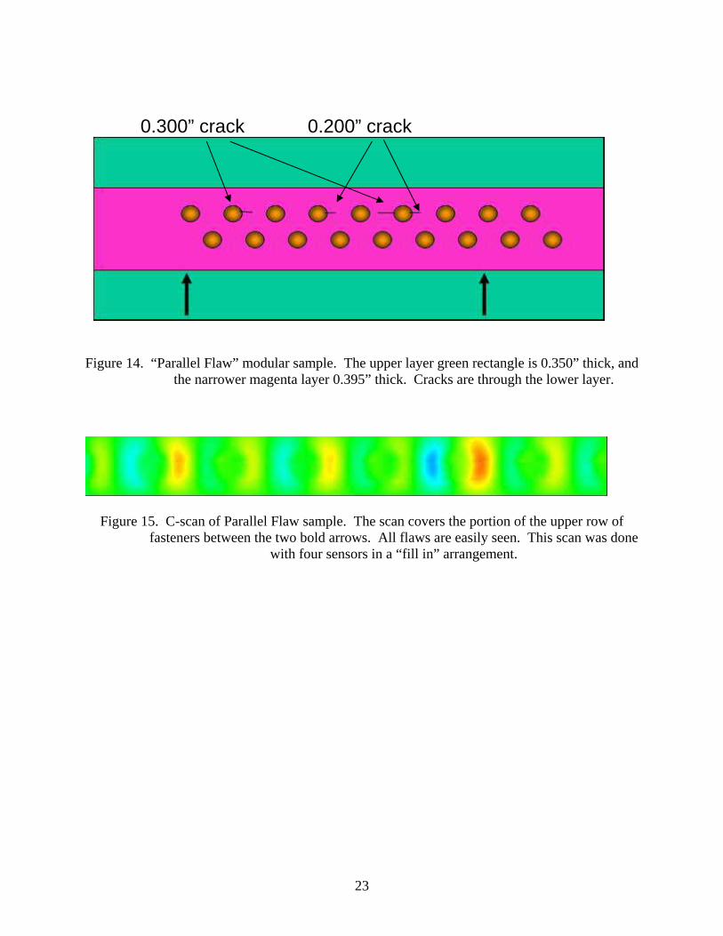
Figure 14. “Parallel Flaw” modular sample. The upper layer green rectangle is 0.350” thick, and the narrower magenta layer 0.395” thick. Cracks are through the lower layer. ... 23
Figure 15. C-scan of Parallel Flaw sample. The scan covers the portion of the upper row of fasteners between the two bold arrows. All flaws are easily seen. This scan was done with four sensors in a “fill in” arrangement. ....................................................... 23
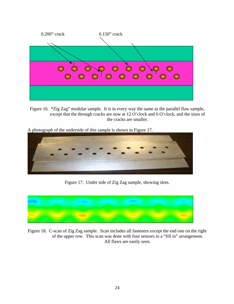
Figure 16. “Zig Zag” modular sample. It is in every way the same as the parallel flaw sample, except that the through cracks are now at 12 O’clock and 6 O’clock, and the sizes of the cracks are smaller. .................................................................................................. 24
Figure 17. Under side of Zig Zag sample, showing slots. ........................................................... 24
Figure 18. C-scan of Zig Zag sample. Scan includes all fasteners except the end one on the right of the upper row. This scan was done with four sensors in a “fill in” arrangement. All flaws are easily seen........................................................................ 24
Figure 19. “Step crack” modular sample. The lower layer has cracks all at 6 O’clock with lengths as shown. ......................................................................................................... 25
Figure 20. C-scan of “Step Crack” sample. All fasteners on lower row are shown except the two end ones. This scan was done with a four sensor “fill in” arrangement. ............. 25
Figure 21. KC-135 360 Wing Splice sample. There are three layers on the left, and two on the right. The horizontal gap has a crack in the second layer. Fasteners are ferrous, and several cracks have been cut into the second layer. The lower two rows of fasteners are larger than the upper two rows............................................................................... 25
Figure 22. Sketch of 360 wing splice specimen. Upper layer of splice has a gap approximately 0.125” wide, in which there is a crack as well. The right half of the specimen has a third layer, and the left has only two layers. All fasteners are ferrous. There are four cracks in the second layer, as shown in the sketch............................................... 26
Figure 23. Scan of 360 wing splice sample. Note “Halos” at positions of cracks, and the less intense and nonetheless obvious splice crack. ............................................................. 27

vi
List of Figures (concluded) Figure Page
Figure 24. C-scan taken of 360 wing splice with 32-element GMR imaging array mounted on the MAUS platform. Four “problem areas” are easily seen at a glance, and indicated by the arrows. Dashed arrow indicates the splice crack, with a far smaller signature. ...................................................................................................................... 28
Figure 25. C-Scan of Parallel Flaw sample, taken with 32-element array. All of the second layer cracks are easily seen. This is typical of what can be routinely achieved with a GMR array that is properly operated......................................................................... 28
Figure 26. C-scan of Parallel Flaw sample with 0.100 insert that has through slots, which simulate notches at the top of a thicker second layer. Lower row is same as in figure 25, with through notches in the bottom 0.395” layer. Upper layer is 0.350” thick.............................................................................................................................. 29
Figure 27. Scan in Figure 21 with contrast adjusted for a “go-no go” indication. All flaws detected without the squeezing are more easily seen, and appear at a glance. ............ 30
Figure 28. Four layer 777 Sample, with third layer notch sizes indicated. An edgewise view of the sample is shown in Figure 29. ........................................................................... 31
Figure 29. Edgewise upside down view of 777 sample shown in Figure 28. The thicknesses of the layers are as follows: 0.100”, 0.125”, 0.160”, and 0.150”. The 0.150” layer is the narrower one on the top in this photo. All fasteners are titanium. ........................ 31
Figure 30. Scan of 777 sample in same orientation as Figure 28. All flaws are seen, and sensors are saturated even for the smallest 0.010” notch in the third layer. ................ 32
Figure A-1. Sheet of current coming in from the left is forced to bend around the hole, bunching it up at top and bottom, creating stronger field in those locations. The laws of physics further require that the field will be pointing up at 12 o’clock, and down at 6 o’clock. ........................................................................................................ 40
Figure A-2. C-scan obtained with MR sensors of a hole for configuration of figure one. The two regions that are not green in the figure indicate stronger field resulting from the fact that the current was “bunched up”. ....................................................................... 40
Figure A-3. Current distribution for fastener hole with a small crack at 12 o’clock. .................. 41
Figure A- 4. C-scan of fastener hole with small crack at 12 o’clock........................................... 42
Figure A-5. Current redirected around a fastener hole with a large crack at 12 o’clock. Note that current is bunched up some at 6 o’clock, and a lot at 12 o’clock. ........................ 43
Figure A-6. C-scan of a fastener hole with a larger (0.200”) flaw at 12 o’clock. ....................... 43
Figure A-7. C-scan of a fastener hole with an even larger (0250”) flaw at 12 o’clock............... 44
Figure A-8. Scan with flaws parallel to fastener row and current perpendicular to fastener row. .............................................................................................................................. 44

1
MULTI-LAYER CRACKS AND MULTI-SITE DAMAGE NDE CONTRACT
Final Report
31 October, 2005
This report covers effort for the Multi-layer Cracks and Multi-site Damage NDE contract commencing on July 1, 2003 and finishing on October 31, 2005.
SUMMARY
This report describes the exploitation of the attractive performance of magnetoresistive (MR) sensors for NDE of metallic aircraft structure, into an imaging array for rapid scanning, and the demonstration of the performance of that array. There were a number of issues requiring resolution for this development. These included array geometry, excitation geometry, signal processing, software, calibration, and operation. The geometry chosen was a linear array with sensitivity axis normal to the surface being scanned, and the excitation geometry is that of a uniform current “sheet”. The array has been initially demonstrated on several test samples, and shown to be able to detect small flaws/cracks at depths of upwards of one-half inch. In many cases, cracks with length only a fraction of the covering metal are easily seen with no additional data manipulation. The array has been integrated and demonstrated with the MAUS scanning platform. Because of the chosen geometry, dependence on circular symmetry is obviated, and therefore rapid scanning along a row of fasteners is possible, with real time imaging. In the future, the bounding of applicability of the array for Air Force inspection scenarios must be determined, as well as flaw signature enhancement through additional processing. The bounding of performance should include stack up configurations, thicknesses, material types and combinations, and flaw depth and size. In addition, probes for “niche” applications should be addressed and where appropriate developed. Work on determination the dependence of calibration parameters on depth should be undertaken, as well as the usefulness and quantification of employing more than one excitation frequency. Quantification of the superior performance of MR sensors in comparison to conventional eddy current, pulsed eddy current, and magneto-optical imaging is also recommended.
2
1.0 INTRODUCTION
This contract covers the development and demonstration of an imaging array of magnetoresistive (MR) sensors. The effort constituted follow-on to previous work done by Boeing Phantom Works for AFRL Materials Directorate, contract number 02-S437-030-C1 entitled “Magnetoresistive Sensors for Imaging NDE”. The final report for that effort is herein referenced. The primary objective of the effort was to develop the array, and demonstrate its capability to rapidly detect flaws such as cracks lying deeply beneath the surface of metallic aircraft structure. The various parameters affecting the design, operation, and functioning of the array were investigated, a final configuration defined, and the array was built. Along the way, a number of different critical issues were resolved, leading to the final design. The array was used to scan a number of specimens verifying its ability to detect deeply lying cracks, as well as simulated corrosion regions in a number of representative specimens. These specimens typically were 0.4 inch or greater in thickness and had flaws and cracks of various sizes. Cracks as small as one tenth of the thickness of the covering metal were “seen”, with cracks of one fourth the size of the covering metal being routinely detected with no augmentation or massaging of the raw data. This scanning was accomplished with a laboratory X-Y bridge. The array was then engineered for scanning with the MAUS platform, and demonstrated at Tinker Air Force Base on October 6th, 2005. This report covers the development of the imaging array, including discussion of the significant issues encountered during the development.

3
2.0 ARRAY DEVELOPMENT
2.1 General The previous contract established the usefulness and attractiveness of MR sensors, and anisotropic magnetoresistive sensors (AMR) in particular. The present effort has furthered the work, incorporating giant magnetoresistive (GMR) sensors, which were not developed to the point where they were as attractive at the time. We are now satisfied that the GMR sensors may be integrated in arrays, and successfully used for imaging NDE work in aircraft. The steps and major issues in developing a fully functional array using GMR sensors are detailed in this section of the report.
2.2 Selecting GMR Sensors There are several issues that needed resolution to incorporate GMR sensors as the “workhorse” for the array. The first of these was verifying that they were worth the change. In terms of size, they are roughly comparable to the AMR, but in terms of sensitivity, they are several times better. We could see smaller features at a greater depth with the GMR sensors than we could with the AMR. An example of this is shown in Figure 1. We see cracks, which are all located at 6 O’clock on the fastener holes, down to one tenth the thickness of the 0.350” covering metal.
Figure 1. Scan with GMR sensors of specimen with a 0.350” layer covering a 0.395” layer. Dimensions are the lengths of the through cracks in the bottom layer.
Figure 2 shows a scan of a sample with larger cracks, taken with the 64-element AMR array developed in the previous contract. The lines in the scan are due to the inequality of the sensor responses, and the differences in residual field at the locations of the various sensors.
none 0.035” 0.076” 0.117” 0.146” 0.199” 0.249”

4
Figure 2. Scan done with AMR sensors of specimen having the same thickness for both layers as
that of figure 1. Dimensions are for cracks at both 12 O’clock and 6 O’clock. The second significant issue in arriving at GMR, is the fact that they have a far larger range of bias field over which they have a linear response. The range for the AMR is about 1.5 to 2 Oersted, where as it is approximately 30 Oersted for the GMR. With such a large range, it is possible to bias all of the sensors in the array with a single source, rather than having to do each one individually. This translates into a considerably less complex amount of circuitry. With the AMR, each sensor would have to employ its own feedback signal, which would be used to adjust the current in its bias coil. The advantage of individual biasing is that changes in the background field are automatically compensated. With the GMR, it is not necessary to worry about changes in the background field, unless they are of the order of 10 Oersteds, which is about twenty times the magnitude of the earth’s field. Due to the higher sensitivity of the GMR sensors, it is not necessary to place them as close together for the same results. Therefore, fewer sensors will perform with the same fidelity as the larger number required using AMR sensors. The 64-element AMR sensors used in the previous contract constituted an array approximately 0.8 inch wide. We were able to get equivalent fidelity using only 32 sensors over a space of 1 inch using GMR sensors. This reduces the complexity of circuitry and routing, as well as the amount of bandwidth required to perform signal processing, since there are fewer channels. Before concluding that the GMR sensors would work best, we did some scanning with off the shelf individually packaged sensors. These were “tilted up” on the edge of their SOIC8 packages, which placed the sensitive bridge about 2.5 millimeters above the surface of the flexible excitation board. We achieved very good performance with the sensors mounted in this way, and this allowed us to conclude that the arrays, with much smaller sensor standoff distances, would not experience compromised performance due to this issue. The scan shown in Figure 1 was made with individually packaged sensors.
0.300” cracks 0.200” cracks

5
Finally, the GMR sensors appear to be no less rugged than the AMR, and possibly a little more able to take physical abuse.
2.3 Excitation Current Geometry In order to preclude the complexities associated with circular excitation coils, and to reduce the amount of excitation field in the vicinity of the sensors, a current in the form of a “sheet” comprises the best configuration. For rapid scanning and imaging, a swath considerably larger than that produced from a single sensor must be taken. In order for all sensors to be directly comparable and contributing to the image, they all must experience the same current. This has been discussed in the report from the previous contract. The preferred excitation geometry is a sheet. An example of a mask for producing such a sheet is shown in Figure 3. After the mask is made, the traces are deposited on a piece of thin and flexible fiber glass epoxy circuit board material. The actual dimension of the excitation board, is four inches square. The signal providing the excitation is generated in the A to D converter, and sent to an amplifier to provide the boost up to several hundred milliamps. The current carrying traces, in the shape of “ribbons”, in the wider central region of the board, all have current in the same direction. The return traces for the individual ribbons are located along the sides of the board. In a region near the center of the board, the current is reasonably uniform, and especially so at distances of less than a ribbon width from the center. Along the geometric center of the board, there is no net field in the direction normal to the surface of the item being scanned.

6
Figure 3. Mask drawing for exciter board, that produces a “sheet” of current in the central section. The current is constant across the board anywhere above this sheet. A thin
(<.003”) layer of Mylar tape is applied to the board to prevent shorting by the metallic specimen being scanned.
2.4 Orientation of Sensors Work under the previous contract has shown that the field component resulting from interaction of deep flaws with surface-injected eddy current, especially for sheet current geometries, is the component normal to the surface being scanned. The design of the 32-element array with its one inch wide swath incorporates this orientation of the sensors. We also considered adding another set of sensors that were oriented parallel to the sheet current conducting ribbons, but analysis and

7
experimentation concluded that it did not produce sufficient improvement to justify the extra complexity and expense. In the future, it may be advisable to revisit this possibility, especially if circuitry lock-in amplifiers have become the norm.
2.5 Energizing/Controlling the Sensors The sensors are deposited on their substrate as full Wheatstone bridges. The bias supply for all of the sensors is the same, so that they are connected in parallel to a single D.C. source. A single “strap” provides a field sufficient to bias each of them at a point at or near the center of their linear response range. This strap is deposited near the sensors as part of the manufacturing process. A current of zero to one amp biases the sensors for optimal operation. As mentioned, the sensors are configured as Wheatstone bridges. The imbalance signals of the bridges are fed to instrumentation amplifiers with fixed gain before being passed along for demodulation. The bridge circuit which is used for each of the 32 sensors is shown in Figure 4, along with the circuitry providing the bridge bias, the current to the bias strap, and the excitation to the coil providing the sheet current. The out puts of the instrumentation amplifiers are fed into the A to D. This digitizes the signals, which are essentially modulated versions of the excitation signal. Once digitized, the signals are computationally demodulated into two channels per sensor, as described in the next section. For instances where electronic demodulation is used, the demodulation is performed before the digitization, so that each sensor provides two signals to the A to D, instead of one. These two signals are in quadrature. Due to the significant reduction of space, volume, and complexity required by the circuitry, demodulation done computationally is preferable. In order to demodulate in this way, however, averaging must be performed, which takes several (5 to 10) cycles of the excitation signal. With 32 channels, the amount of bandwidth pushes the capacity of the A to D. For this reason, there is an UPPER LIMIT to the excitation frequency that can be successfully used, when demodulating computationally. This stands in stark contrast to conventional eddy current technologies which experiences have low frequency limitations. For higher frequency operation, it will be necessary to employ electronic demodulation means. As the bandwidth of A to D systems continues to rise, the routine operating frequency for systems using computational demodulation means will rise accordingly.

8
Figure 4. Circuitry schematics for GMR imaging array, and excitation coil driver.
2.6 Signal Processing Issues
2.6.1 Calibration/Initialization of the Array Even though the sensors in the array are simultaneously deposited on a single substrate (actually two identical substrates of 16 sensors each), they still have slightly different “zero bias” points as well as differing responsivities to the same perturbing field signal. For this reason, it is necessary to balance out the offset of each individual sensor, as well as normalize their individual responsivities or gain factors.

9
Historically we have done this by placing the array on a thick piece of aluminum, far away from its edge as seen in Figure 5. We then energize the sensors with an excitation of the amplitude and frequency that will be used for the inspection. The output of each sensor is noted, and a file is saved of these outputs. Each one of these values is then subtracted from the output of its respective sensor, so that all of the sensors are “balanced” or “zeroed”. Look up tables are constructed of these balancing values for each of the sensors, for various values of amplitude and frequency. We have not attempted at this point to investigate the dependence on the balance values with specimen thickness, but this is something that we plan to look into in a subsequent effort.
Figure 5. Photograph of sensor head positioned on the calibration sample. The Sensors are shown in the position where the balance values are measured for each of the 32
sensors. The sensor head is then moved across the surface slot, which is also shown in the photograph. Integration over the responses of each sensor across this slot is
done to determine the gain factors. In order to normalize the responsivity of each of the sensor, so that they respond as equally as possible to the same input after balancing, we slowly move the entire array across a very large “flaw” which has been machined into the calibration specimen as seen in Figure 5. We then assign a multiplier to each sensor so that the response of each sensor is the same. The multiplier is calculated by taking the ratio of the area under the curve of each response to that of a selected reference sensor. The reference sensor can be any of the sensors, but is usually selected as one near “the middle of the pack”. These normalization data are also stored in look up tables, for typical values of excitation amplitude and frequency. After both of these values are assigned to the sensors, data acquisition can commence. As discussed in Section 2.7 below, the demodulation and calibration of the data is done completely in software instead of hardware. Details of the calibration algorithm will be elaborated in that section.

10
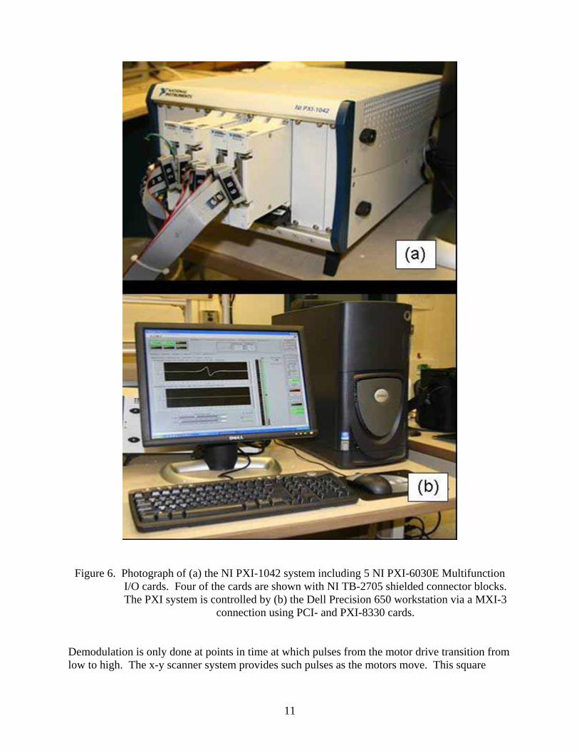
2.6.2 Data Acquisition The data acquisition hardware consists of up to five 16-channel analog input ports located on NI PXI-6030E Multifunction I/O cards that are installed in a NI PXI-1042 chassis as shown in Fig. 6 (a). The chassis is connected to a Dell Precision 650 workstation, as seen in Fig. 6 (b), via the NI PCI- and PXI-8330 MXI-3 system. The PXI-6030E cards are multi-function DAQ platforms that also provide digital IO as well as analog output capabilities. One card provides a “seed” excitation waveform that is further amplified through hardware to provide the excitation current to the coil. This card also provides the same seed waveform in quadrature. Both of these signals are read directly back into separate analog input channels for demodulation processing, as discussed in Section 2.7. Full waveform data from each of the 32 sensors is acquired by two of the A/D cards (16 channels each) at a typical digitization rate of 15 kS/s (kilo-Samples per second). These particular cards have a maximum sampling rate of 1.25 MS/s divided by the number of analog input channels used. This results in a maximum digitization rate of about 78 kHz over 16 channels. To adequately resolve a waveform, it is desirable to have approximately 10-12 samples per signal cycle, resulting in a theoretical maximum excitation frequency of 7-8 kHz. In practice, however, the maximum excitation frequency is about half this, on the order of 3-4 kHz due to computational speed limitations. This limitation is partly dictated by computer speed and partly by numerical accuracy. This upper limit is typically further reduced to about 2 kHz due to the added computational burden of data visualization and other program “overhead” tasks. The full waveform data is acquired in typical data buffer sizes of 6000 samples. Due to the nature of the demodulation algorithm, it is necessary to retain 3 successive buffers in computer memory at a time. The processing is done on the middle buffer, overlapping with the first and last buffers as necessary. Demodulation is done by averaging over typically ten periods of the waveform. Hence the need for so many samples in the buffer as well as overlapping buffers.
11
Figure 6. Photograph of (a) the NI PXI-1042 system including 5 NI PXI-6030E Multifunction
I/O cards. Four of the cards are shown with NI TB-2705 shielded connector blocks. The PXI system is controlled by (b) the Dell Precision 650 workstation via a MXI-3
connection using PCI- and PXI-8330 cards.
Demodulation is only done at points in time at which pulses from the motor drive transition from low to high. The x-y scanner system provides such pulses as the motors move. This square
12
wave signal is divided down in frequency to provide a more reasonable resolution of motor pulses, approximately a pulse for every 0.01 inches of motion. This motor pulse rate division, and hence the resolution of the scan, is configured by some hardware electronics, that are controlled by digital output. For the MAUS system, the MAUS hardware provides the motor pulses as necessary. Demodulation is done over a window of waveform data centered about each upward pulse transition. Again, the size of this pulse is typically equal to ten periods of the excitation period. The demodulated and calibrated data is then stored in memory for both visualization and storage. The mathematical derivations relating to these demodulation and calibration procedures are given in Section 2.7, along with graphical illustrations of the waveform buffering and averaging.
2.6.3 Phase Adjustability The regime where the demodulated signal is most sensitive to the small modulations resulting from small or far away flaws is near the point where the NET phase of the signal is at or close to ninety degrees. In order to make sure that system operation can be placed as closely as possible to this point, it is highly recommendable to introduce a continuously variable detection phase which can be varied through 360 degrees. The software which we have developed employs a slide bar that can be adjusted to within a millidegree or two. The detectability of flaws, especially those that are small, or far away (deep), is highly dependent on the adjustment of the detection phase. It is not difficult to quickly arrive at the best possible rendition of a scan, since the calculations are done in essentially real time once the scan is completed. But this depends on having capability to continuously vary the detection phase.
2.6.4 Gradient Plots In some cases, it is of interest to plot the in-plane spatial gradient(s) of the field signals for C-scans. We investigated the attractiveness of doing this by common mode rejection of output from adjacent sensors, by direct electronic subtraction of signals from adjacent sensors, and by computation. We found that in general, determining the gradients by computation instead of electronically gave us no loss of generality or sensitivity. In actuality, it is better to do it computationally, since the resolution can be better than when arranging individual sensors. Figure 7 shows the configuration of two sensors that were used to make a gradient scan. Figure 8 shows the common mode rejection configuration of the sensor outputs, for a gradient of the field component normal to the specimen surface, with respect to the coordinate that is vertical in the scan. The excitation is the current sheet previously described.
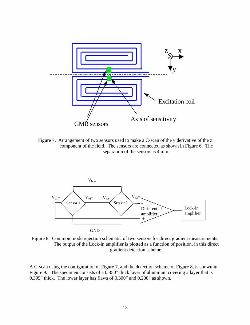
13
Excitation coil
GMR sensorsAxis of sensitivity
x
y
z
Figure 7. Arrangement of two sensors used to make a C-scan of the y derivative of the z component of the field. The sensors are connected as shown in Figure 6. The
separation of the sensors is 4 mm.
Vo1+ Vo1- Vo2- Vo2+
Vbias
GND
-
+
Sensor 1 Sensor 2 Lock-in amplifier
Differential amplifier
Figure 8. Common mode rejection schematic of two sensors for direct gradient measurements.
The output of the Lock-in amplifier is plotted as a function of position, in this direct gradient detection scheme.
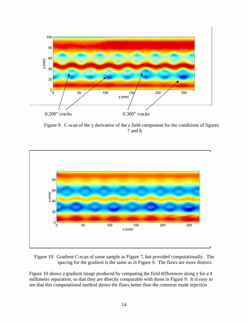
A C-scan using the configuration of Figure 7, and the detection scheme of Figure 8, is shown in Figure 9. The specimen consists of a 0.350” thick layer of aluminum covering a layer that is 0.395” thick. The lower layer has flaws of 0.300” and 0.200” as shown.
14
0.200” cracks 0.300” cracks Figure 9. C-scan of the y derivative of the z field component for the conditions of figures
7 and 8.
Figure 10. Gradient C-scan of same sample as Figure 7, but provided computationally. The spacing for the gradient is the same as in Figure 9. The flaws are more distinct.
Figure 10 shows a gradient image produced by computing the field differences along y for a 4 millimeter separation, so that they are directly comparable with those in Figure 9. It is easy to see that this computational method shows the flaws better than the common mode rejection

15
method. This is due to the difficulty of scanning over the exact same lines with the two sensor configuration, versus the one sensor configuration, and small alignment inconsistencies. In general, computational gradients are at least as good, if not better than those that are directly detected. Performing the gradient function in software is considerably less complicated than with circuitry. It also requires less real estate on the circuit cards. It gives good results, and because of these things it is the recommended way of obtaining gradient plots. The computational resolution is as good as the polling process used to produce the image. Typically, when scanning in the lab on the X-Y bridge, we poll every 0.01 second, and at 1 inch per second scan speed, this translates into a gradient established between each set of data points at 0.01 inch apart. This kind of resolution is more than sufficient for visual inspection of the resulting C-scans. In general, the density of gradients points can be equal to the density of field points, when performing the differentiation computationally.
2.7 Signal Demodulation The signals output from the sensors are AC waveforms at the drive (excitation) frequency, as modulated by the features and “terrain” over which they are scanned. The modulation is in amplitude and phase as referenced to the phase of the current in the excitation “coil”. The modulations experienced by the individual sensors can be quite large, especially for prominent features such as fastener holes, or very large cracks. In turn, sensors located well away from large features may experience little or no modulation. In order to successfully detect the minute signals arising from the redirection of induced eddy currents with deeply lying features (flaws), phase sensitive detection is employed. Historically, lock-in amplifiers have been circuits employing a high Q tuned oscillator of variable phase, a mixer and a low pass filter. The input signals arriving from the sensors are mixed with a variable phase copy of the excitation signal. The result is low pass filtered, providing a DC signal which is proportional to the strength (amplitude squared) of the modulation of the excitation signal which is phase dependent. The phase is then adjusted to maximize this signal, which almost always occurs at or near the quadrature point. In order to be completely general, and to preclude the possibility of losing the signal, the mixing is done with both a signal in phase with the excitation, and one at quadrature with it. As shown below, the general expression for demodulation of the information impressed on the carrier (excitation) signal depends on both of these signals, and is a non-vanishing phase dependent signal. It is this signal that is displayed to form a C-scan. In order to reduce volume and electronic complexity, we developed a method of performing the lock-in function in software. This is detailed in the following sections.
16
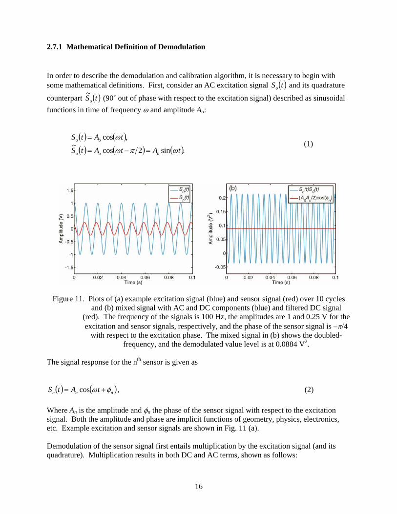
2.7.1 Mathematical Definition of Demodulation In order to describe the demodulation and calibration algorithm, it is necessary to begin with some mathematical definitions. First, consider an AC excitation signal ( )tSo and its quadrature
counterpart ( )tSo~ (90˚ out of phase with respect to the excitation signal) described as sinusoidal
functions in time of frequency ω and amplitude Ao:
( ) ( )( ) ( ) ( ).sin2cos~
,cos
tAtAtS
tAtS
ooo
oo
ωπω
ω
=−=
= (1)
Figure 11. Plots of (a) example excitation signal (blue) and sensor signal (red) over 10 cycles and (b) mixed signal with AC and DC components (blue) and filtered DC signal
(red). The frequency of the signals is 100 Hz, the amplitudes are 1 and 0.25 V for the excitation and sensor signals, respectively, and the phase of the sensor signal is –π/4
with respect to the excitation phase. The mixed signal in (b) shows the doubled-frequency, and the demodulated value level is at 0.0884 V2.
The signal response for the nth sensor is given as
( ) ( )nnn tAtS φω += cos , (2) Where An is the amplitude and φn the phase of the sensor signal with respect to the excitation signal. Both the amplitude and phase are implicit functions of geometry, physics, electronics, etc. Example excitation and sensor signals are shown in Fig. 11 (a). Demodulation of the sensor signal first entails multiplication by the excitation signal (and its quadrature). Multiplication results in both DC and AC terms, shown as follows:

17
( ) ( ) ( ) ( )
( ) ( )
( ) ( ) ( ) ( ).2sin2
sin2
~
,2cos2
cos2
coscos
nno
nno
on
nno
nno
nnoon
tAAAAtStS
tAAAAttAAtStS
φωφ
φωφ
φωω
++=⋅
++=
+=⋅
(3)
Equation (3) illustrates the DC component and double-frequency AC component present in mixing two signals of the same frequency. The second step in demodulation is the removal of the AC component through some kind of filtering. The computer algorithm accomplishes this in a simple fashion through integration of the mixed signal over time. By averaging over an integral number of excitation cycles, namely
ωπ /2 nTn = , the AC term vanishes, leaving only the DC term:
( ) ( )
( ) ( ) ( ).cos2
2sin4
cos2
,2cos2
cos2
/2
0
000
nno
nt
tn
non
no
nT
nno
nno
nT
on
AAtn
AAAA
dttAAAAdtSS
φφωπ
φ
φωφ
ωπ
=++=
⎟⎠⎞
⎜⎝⎛ ++=⋅
=
=
∫∫ (4)
The quantity defined in Eq. (4) is referred to as the demodulation result of the nth sensor with respect to the excitation at “zero detection phase.” The demodulation of the example signal in Fig. 11 (a) is shown in Fig. 11 (b). Demodulation of the sensor with respect to the quadrature excitation signal at zero detection phase is equivalent to demodulation with respect to the excitation at π/2 (or quadrature) phase:
( ).sin22
cos2
~2 n
non
noonoon
AAAASSSS φπφπ
=⎟⎠⎞
⎜⎝⎛ −=⋅=⋅ (5)
Finally, demodulation of the signal at an arbitrary detection phase can be expressed as a mixing of the in-phase and quadrature demodulation components as follows:
( )
( ) ( ) ( ) ( )
( ) ( ).sin~cos
sinsin2
coscos2
cos2
00δδ
δφδφ
δφδ
onon
nno
nno
nno
on
SSSS
AAAA
AASS
⋅+⋅=
+=
−=⋅
(6)

18
It is therefore only necessary to compute and store the in-phase and quadrature demodulation component data. The C-scans are images of these two components over the scan area as mixed together using a user-defined detection angle δ as shown in Eq. (6). This detection angle is typically chosen to best enhance any features of interest, such as cracks or other flaws.
2.7.2 Mathematical Definition of Calibration As discussed in Section 2.6.1, the data is calibrated by subtracting a “balance” value from the demodulated result. This balance value is obtained by computing the in-phase and quadrature demodulated values on a thick sample far removed from edges and any flaws. The calibrated form of Eq. (6) is therefore expressed as follows, where prime denotes the sensor signal obtained at the calibration point:
( ) ( ) ( ) ( ).sin~~cos
0
/
00
/0
δδδ ononononon SSSSSSSSSS ⋅−⋅+⋅−⋅=⋅ (7)
The double brackets in Eq. (7) denote calibrated demodulation. It can be shown algebraically that this action is equivalent to subtracting the raw sensor signal waveform by the zero-balanced sensor signal obtained at the calibration position. Letting ( )tSn
/ be the calibration sensor signal, we calibrate the sensor signal as:
( ) ( ) ( ) ( )/// coscos nnnnnn tAtAtStS φωφω +−+=− . (8) Demodulating this with respect to the excitation signal at arbitrary detection phase δ yields:
( ) ( ) ( )
( ) ( ) ( ) ( )
( ) ( ) ( ) ( )
( ) ( ) ( ) ( )
.
sin~~cos
sinsin2
coscos2
sinsin2
coscos2
cos2
cos2
0
/
00
/0
//
//
//
/
δ
δ
δδ
δφδφ
δφδφ
δφδφ
on
onononon
nno
nno
nno
nno
nno
nno
onn
SS
SSSSSSSS
AAAA
AAAA
AAAASSS
⋅=
⋅−⋅+⋅−⋅=
−−
+=
−−−=⋅−
(9)
It is clear that Eq. (9) is the same as Eq. (7), and therefore subtraction of raw calibration waveform prior to demodulation is equivalent to subtraction of demodulated calibration values after demodulation of raw signal.

19
It was also discussed in Section 2.6.1 that each sensor requires a “post-demodulation” gain factor due to some variation in the sensitivities of the 32 sensors. To complete the mathematical derivation of calibrated demodulation, therefore, the gain factor αn must also be included:
( ) ( ) ( ) ( )[ ].sin~~cos0
/
00
/0
δδαδ ononononnon SSSSSSSSSS ⋅−⋅+⋅−⋅=⋅ (10)
2.7.3 Demodulation Example Now that the mathematical representation of demodulation and calibration has been formalized, it is illustrative to present an example of the algorithm in action. The calibration sample, shown in Fig. 12, provides a convenient example. An excitation signal identical to the mathematical example of Fig. 11 was set used: amplitude Ao = 1 V and frequency f = 100 Hz. First, the sensors were scanned across the calibration sample slot, the results of which are shown in a line plot in Fig. 12 (a). The 32 sensor’s raw demodulation values are represented here at a detection phase of δ = 150º over an 8-inch scan. The spread of the “zero balance values” can be seen in the variance of the demodulated values to the left and right of the slot. The sensors were scanned across the slot again after having measured the balance calibration values, as seen in Fig. 12 (b). Now it is clear to see that the zero balance has been corrected. Again the sensors were scanned across the slot after adjusting for their respective gain factors, as seen in Fig. 12 (c). Here it is clear to see that all 32 sensors have reasonably the same adjusted sensitivity across the calibration sample.
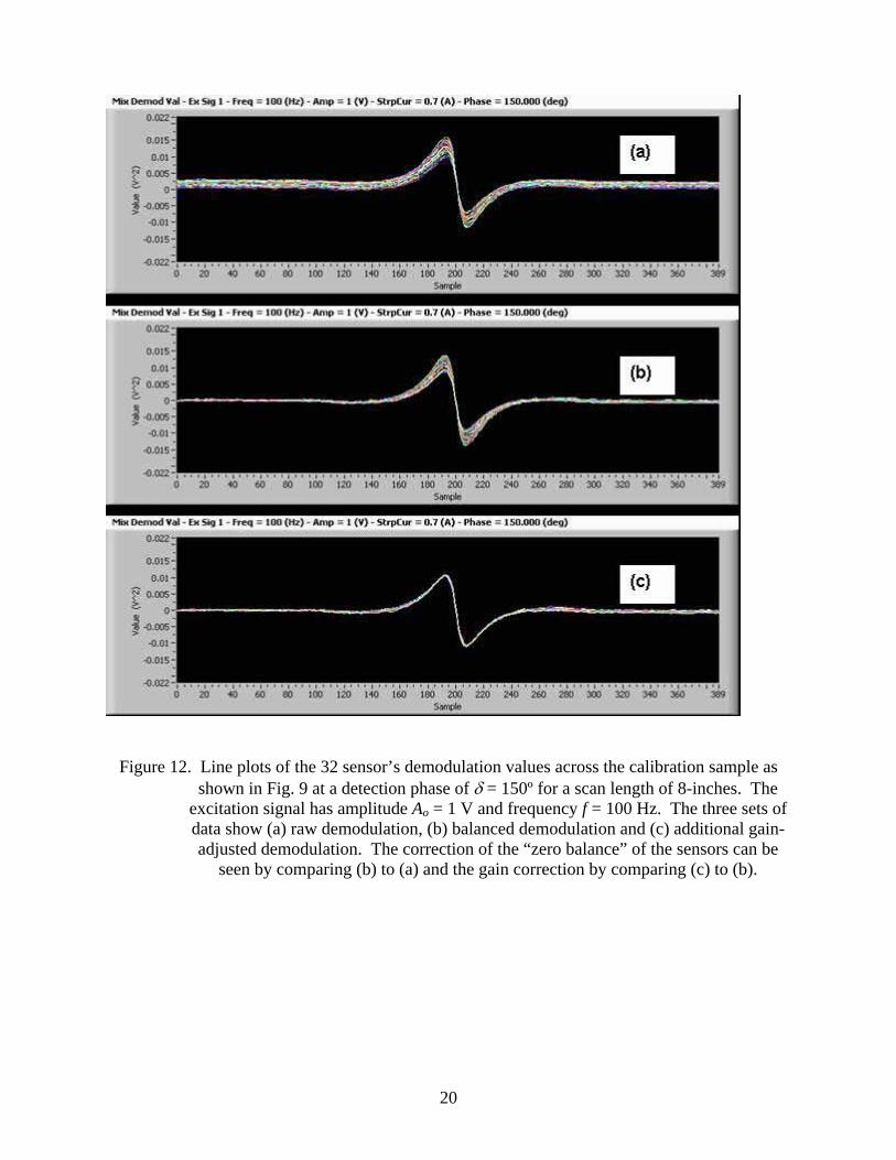
20
Figure 12. Line plots of the 32 sensor’s demodulation values across the calibration sample as
shown in Fig. 9 at a detection phase of δ = 150º for a scan length of 8-inches. The excitation signal has amplitude Ao = 1 V and frequency f = 100 Hz. The three sets of data show (a) raw demodulation, (b) balanced demodulation and (c) additional gain-adjusted demodulation. The correction of the “zero balance” of the sensors can be
seen by comparing (b) to (a) and the gain correction by comparing (c) to (b).

21
3.0 SCANNING WITH 32-ELEMENT GMR ARRAY
3.1 General The 32-element imaging GMR array was developed with the help of a laboratory X-Y scanning bridge. Software was written in LabVIEW that permitted a reasonably detailed and generalized number of options so that the array performance could be optimized. This software provided for the full control and adjustment of the array from the host computer. The operator could input frequency, amplitude, number of sensors, perform either a manual calibration or use a look up table for initialization, manipulation of the size and portion of a given C-scan, and selection of a color pallet for display. In addition, the software provided for contrast sliding and squeezing, and displaying of images with automatic or preset range. The software also provides for computation and display of in-plane gradients for any C-scan. A number of other diagnostic capabilities are also possible with the system control software.
3.2 Scope of Scan Studies Since the effort concentrated mainly on developing a demonstrating the imaging array, we did not do a great deal of scanning. We did, however scan some samples containing deep flaws ranging from easy to detect, to the very difficult. The encouraging results of the scanning in an overall sense are that with care, cracks far smaller and deeper than can be detected with conventional eddy current technology can be routinely detected. Originally, it was envisioned that a ‘round robin” competition would be undertaken with Boeing, Albany Instruments, and NASA Langley. As it turned out, Albany Instruments did do some scanning, but NASA Langley came in at far too expensive. So instead of a competition, we arranged for Albany Instruments to do some studies for us, and their results were very close to ours for the modular specimens that were developed for the round robin exercise. The scans shown in figures 9 and 10 were made by Albany Instruments. During the development of the array, we tried several configurations to ensure that when we submitted the requirements for the final array, they would be for the best that we thought we could do. For this reason, earlier in the program we ran with 1, 2, 4, and 16 sensors, as well as two banks of 16 sensors that were slightly separated. When the final 32-element arrays were delivered, it was quite late in the contract, and therefore we did not do a great deal of scanning with those arrays. We did confirm, however, that the arrays do work very well, (at least for the two we put through their paces). Follow-on work would bound the expectable performance of the arrays. The modular specimens used for much of the scanning work done on the contract were made of two layers of aluminum, with a 0.350” thick layer covering a 0.395” layer. There were two

22
staggered rows of fastener holes that were 0.375” in diameter, with the holes in the upper layer countersunk to the standard 100 degrees. The lower layer, in which slots were made by EDM, was narrower than the upper layer. There were various lower layers that could be affixed to the upper layer, affording modular interchangeability. We typically used the once called the “parallel flaw”, although the zig zag”, and the “step crack” samples were used earlier in the program, before the 32-element array became available from NVE. Figure 1 is a C-scan of the step crack specimen, and figures 9 and 10 are scans of the zig zag specimen. We also had opportunity to scan a sample simulating a 360 wing splice for a KC-135. This sample had ferrous fasteners, and was not quite so thick as the three modular samples described above. There were cracks, which in some cases were covered so as not to be visible from either side, but all cracks were found. Below are shown the three modular samples, as well as the wing splice, and one or more scans of each. In addition to these we briefly looked at other samples, particularly a 777 sample provided by our Wichita location, which had four layers, with notches in the third layer. Using the modular approach for the second layer of the “round robin” specimens, was a very easy way to quickly vary the type and size of deeply lying flaws. For each instance, the number of sensors used to make the C-scan is stated. There is no enhancement of any of the data taken with 4 sensors, other than to squeeze down the contrast. The data taken with 16 or 32 sensors can have contrast squeezed as well, but also can be smoothed, by averaging a “window” that is three sensors in width. In other words, the outputs of each sensor and the ones that are immediately adjacent to it on each side are averaged, and then plotted. Sketches or photos of the applicable samples appear below. For the first two, which are modular, the green rectangle represents the larger 0.350” thick top layer, and the magenta represents the 0.395” thick narrower layer underneath.
Figure 13. Photo of upper layer of the modular samples. The two staggered rows of 0.375” holes are countersunk to accommodate flush fasteners. The dimensions of the sample are 15” long, by 8” wide, by 0.350” thick. All of the interchangeable lower layers are
15” long, by 4” wide, by 0.395” thick.
23
Figure 14. “Parallel Flaw” modular sample. The upper layer green rectangle is 0.350” thick, and
the narrower magenta layer 0.395” thick. Cracks are through the lower layer.
Figure 15. C-scan of Parallel Flaw sample. The scan covers the portion of the upper row of fasteners between the two bold arrows. All flaws are easily seen. This scan was done
with four sensors in a “fill in” arrangement.
0.300” crack 0.200” crack
24
Figure 16. “Zig Zag” modular sample. It is in every way the same as the parallel flaw sample,
except that the through cracks are now at 12 O’clock and 6 O’clock, and the sizes of the cracks are smaller.
A photograph of the underside of this sample is shown in Figure 17.
Figure 17. Under side of Zig Zag sample, showing slots.
Figure 18. C-scan of Zig Zag sample. Scan includes all fasteners except the end one on the right
of the upper row. This scan was done with four sensors in a “fill in” arrangement. All flaws are easily seen.
0.200” crack 0.150” crack

25
Figure 19. “Step crack” modular sample. The lower layer has cracks all at 6 O’clock with lengths as shown.
Figure 20. C-scan of “Step Crack” sample. All fasteners on lower row are shown except the two
end ones. This scan was done with a four sensor “fill in” arrangement. In Figure 20, all cracks are seen, although it must be stated that the signal to noise for the smallest two was quite low. This is, however, a good demonstration of the sensitivity of MR sensors to detect small features that lie deeply within metallic structure.
Figure 21. KC-135 360 Wing Splice sample. There are three layers on the left, and two on the
right. The horizontal gap has a crack in the second layer. Fasteners are ferrous, and several cracks have been cut into the second layer. The lower two rows of fasteners
are larger than the upper two rows.
None None 0.035” 0.076” 0.117” 0.146” 0.199” 0.249” 0.299”

26
Figure 22. Sketch of 360 wing splice specimen. Upper layer of splice has a gap approximately
0.125” wide, in which there is a crack as well. The right half of the specimen has a third layer, and the left has only two layers. All fasteners are ferrous. There are four
cracks in the second layer, as shown in the sketch. The ferrous fasteners serve to bring the field down into a sample. This makes a larger field available for eddy current deeper than for the case of a non ferrous fastener. On the other hand, the field tends to stay in the fastener as well, so that the extent of it penetrating OUTWARD from the center of the fastener is reduced. In Figure 22, there is a red rectangle. This indicates the border of a scan taken with a GMR sensor. The scan is shown in Figure 23, and the splice crack, as well as the three other cracks that are in this section of the sample. The cracks on the fastener holes are indicated by the “halos” on the side of the fastener hole where the crack is located. This is due to the field “leaking” a bit more into the crack, than into the surrounding region. The splice crack has a far smaller signature for two reasons. First, it is not emanating from ferrous material, and second it is in the layer below the surface where the excitation coil is located, and as a result, the signature is reduced due to the 0.170” of liftoff.

27
crack splice crack crack crack
Figure 23. Scan of 360 wing splice sample. Note “Halos” at positions of cracks, and the less intense and nonetheless obvious splice crack.
In Figure 24, a scan is shown of the entire sample. It was taken with the 32-element GMR imaging array using the MAUS platform. All four cracks are seen, as well as the splice crack is hinted at, but not as pronounced. Arrows indicate the positions of the cracks, and the splice crack. This particular scan was taken with a different detection phase than that of Figure 23. The areas with “problems” show up in stark contrast to the other background areas. Figure 23 is taken with the detection phase near the excitation, while Figure 24 is at a phase which is closer to quadrature. The splice crack, in this case, is indicated by a dashed arrow. The scan in Figure 24 was taken with the scan axis not quite parallel to the edge of the sample, and that explains the “skewed” orientation of the fastener rows.

28
Figure 24. C-scan taken of 360 wing splice with 32-element GMR imaging array mounted on the MAUS platform. Four “problem areas” are easily seen at a glance, and indicated
by the arrows. Dashed arrow indicates the splice crack, with a far smaller signature.
When the 32-element arrays finally arrived from the vendor (NVE), we studied the parallel flaw sample more than any other. We scanned the sample first rotated 180 degrees form the orientation as shown in Figure 14. A scan of this sample in this orientation is shown in Figure 25. 0.200” cracks 0.300” cracks
Figure 25. C-Scan of Parallel Flaw sample, taken with 32-element array. All of the second layer
cracks are easily seen. This is typical of what can be routinely achieved with a GMR array that is properly operated.
A quick glance at figure 25 shows that all cracks are easily seen, and that the intensities of their signatures are in approximated proportion to their size. It will also be noticed that there are

29
responses on the opposite sides of the fasteners from the flaws. This is caused by the fact that when the fastener hole has a crack, the cross section of the blockage to current changes. As the crack gets longer, a portion of the current that would normally go around the side with the crack is now diverted around the side without the crack, hence the increased signal. This fact makes larger cracks even more obvious. For cases where a single fastener hole has cracks on both sides, as with the second fastener hole from the left in Figure 25, both of the cracks are “amplified”. We then reconfigured the sample by adding a 0.100” thick piece between the upper and lower layers, making the total stack up 0.845”. We put EDM slots in three of the holes in this new inner layer. These through slots, will simulate notches in the upper portion of a thicker lower layer. In other words, the upper layer remains at 0.350”, but now the effective lower layer is 0.495” thick, but has notches in its upper surface, that go only 0.100” deep. These “notches” were 0.050”, 0.100”, and 0.200” long. A C-scan of the sample in this configuration is shown in Figure 26. 0.050” notch in middle (not seen) 0.200” notch in middle 0.100” notch in middle
0.200 through crack in bottom 0.300” crack in bottom
Figure 26. C-scan of Parallel Flaw sample with 0.100 insert that has through slots, which simulate notches at the top of a thicker second layer. Lower row is same as in figure
25, with through notches in the bottom 0.395” layer. Upper layer is 0.350” thick. As can be seen from the scan, all of the cracks in the lower layer are still easily seen, even though they are all 0.100” deeper than in figure 15. Also, two of the three notches in the middle section are seen, without any problem. Only the 0.050” notch is missed. To further amplify the usefulness of the GMR array technology for rapid area scanning for metallic aircraft structure, contrast squeezing can be employed to transform a C-scan into a “go-no go” type of indication. Many software packages, such as Microsoft Photo Editor to name one, have this type of capability. The scan shown in Figure 26 is enhanced in contrast using this type of imaging utility, and shown in Figure 27. All of the flaws that were detected in Figure 26 are immediately seen. Instead of a large rainbow of colors, there are only six. It is not difficult to effectively threshold any scan in this way, to quickly indicate areas of interest. Once a

30
standard is scanned, the contrast can be adjusted, to match system performance to detection requirements.
Figure 27. Scan in Figure 21 with contrast adjusted for a “go-no go” indication. All flaws detected without the squeezing are more easily seen, and appear at a glance.
In Figure 28 there is a picture of another sample from our 777 program. It has four layers, as shown by the edge photo in Figure 29. The sample has notches extending from the upper row of fasteners at the 12 O’clock position, and from the lower row of fasteners at the 6 O’clock position.
0.200” through crack 0.300” through crack
0.050” notch (not seen) 0.200” notch 0.300” notch

31
12 O’clock: None 0.10” 0.15” 0.20” 0.25” 0.30” 0.35” 0.40” None
6O’clock: None 0.45” 0.50” None None None 0.40” 0.45” 0.50” Figure 28. Four layer 777 Sample, with third layer notch sizes indicated. An edgewise view of
the sample is shown in Figure 29.
Figure 29. Edgewise upside down view of 777 sample shown in Figure 28. The thicknesses of
the layers are as follows: 0.100”, 0.125”, 0.160”, and 0.150”. The 0.150” layer is the narrower one on the top in this photo. All fasteners are titanium.
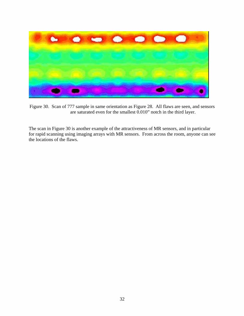
Figure 30 shows a scan taken with the 32 element array. The orientation is the same as shown in Figure 28. All of the flaws are easily seen, and actually cause the sensors to saturate. It is very easy to see even the smallest 0.010” notch in the upper left hand corner. This is a good example of a scan where the current is oriented normal to the line of fasteners, rather than parallel to it.
32
Figure 30. Scan of 777 sample in same orientation as Figure 28. All flaws are seen, and sensors
are saturated even for the smallest 0.010” notch in the third layer.
The scan in Figure 30 is another example of the attractiveness of MR sensors, and in particular for rapid scanning using imaging arrays with MR sensors. From across the room, anyone can see the locations of the flaws.
33
4.0 CONCLUSIONS The program has contributed a number of significant findings and demonstrations concerning the use of MR technology for aircraft NDE. First, we have shown that it is possible to build a functioning array of MR sensors that produces highly sensitive real time images (C-scans) of deeply located small flaws, as the head is translated over a specimen. In so doing we have determined the optimum configuration for such an array, in terms of sensor type (GMR), sensitivity axis orientation, array configuration and sensor density. Second, we have determined the optimal configuration for the excitation current, namely that of a uniform “sheet”. This configuration obviates the difficulties associated with previously used circular symmetry. Third, we have determined how to process the outputs from the sensors to give high fidelity data for image construction. In all of the above, we have successfully exploited the attractiveness of the high sensitivity MR technology to the point where a 32-element linear array of GMR sensors covering a one-inch wide swath, has been designed, built and demonstrated successfully for several specimens with deeply lying cracks. The images are displayed as the data are taken, in what essentially amounts to real time, as the array is scanned along the surface of the specimen at speeds of upwards of one inch per second. In short, we have demonstrated the MR technology successfully, producing real time images of flaws of dimension of only a fraction of the covering metal, at depths exceeding one-half inch. Details of the development process and the operation of the imaging array are outlined in detail in this report. In the following section, we also delineate how the technology can be taken from here to be “spiraled” into the fullest exploitation for current and anticipated Air Force inspection requirements, to becoming the next NDE modality that it is destined to be.

34
5.0 RECOMMENDATIONS FOR FUTURE WORK We have shown the kinds of results that can be obtained when employing MR sensors for rapid area scanning. We have not yet begun to scratch the surface in terms of fully understanding the capabilities of these sensors, and even more specifically as they relate to actual Air Force inspection scenarios. We need to understand where they are the hands down choice, and quantify their capabilities for a variety of inspection scenarios. We need to determine how to best exploit them for investigation of individual fasteners/holes once the rapid scanning has detected a “region of interest”. Pursuant to these overall long term goals we recommend that the following be done.
1) A survey of all inspection scenarios and requirements for appropriate Air Force aircraft should be made. This is to determine the stack up configurations, thicknesses, and even the combinations of materials that could possibly lend themselves to inspection with MR sensing.
Once this information is available, articles representing the scope of inspections should be collected and/or assembled. These can be standards, pieces from actual aircraft, or other specially constructed samples. They should span the expectable range of thickness and configuration, including nearby structural members such as stringers, ribs and spars. The full spectrum of applicable items should then be scanned with the MR imaging array, as a process capability study. The results will permit determination of the expectable depths at which flaws of a specified size might be detectable. In some cases, and actual POD could be determined, but in any case, we would know the capability of the technology as it applies to the gamut of Air Force inspection scenarios. This should be done for instances involving both cracks and corrosion. From performing this scanning, it should be determined if crack length or extent of corrosion regions can be estimated from the MR data. These estimates may be crude, and in other cases they could be simply bounded, and the results would be presented as “crack of at least 0.xyz” length at 0.abc” depth”, or possibly something like corrosion region extending 0.def” inches”.
2) It is certainly true that the depth of operation, and hence the excitation frequency effect
the sensor output. Calibration is currently carried out for a single value of total stack up thickness. A determination should be made of how the two calibration values for each sensor (offset and multiplier) vary as a function of thickness. This variation will be more drastic as the total thickness becomes smaller. Since the preponderance of the work done so far is for very thick samples, the variation was not considered to be a concern, but for the general case, a good understanding of how calibration values change with stack up thickness is useful. Tables including various expectable values of total stack up thickness should be constructed. It could be that stack up thickness will be a parameter for the calibration look up tables.

35
3) From the results of the survey in the first recommendation above, it will be possible to
determine inspections that cannot be accomplished with a large (4” by 4”) footprint array, but may be doable with a “custom” probe of much smaller footprint. It may be that angle bends, or regions replete with complex skeletal structure will require such an inspection method. The superior sensitivity offered by MR sensors may be applied to these as well. These custom inspections should be evaluated for potential MR applicability. In particular, a probe with circular or near circular symmetry should be built using two GMR sensors for inspection of individual fastener holes.
4) In order to demonstrate quantitatively the attractiveness of MR technology to other types
of eddy current, a DOE should be performed that compares MR with Pulsed Eddy Current (PEC), remote field eddy current (RFEC), and Magneto Optic Imaging (MOI). Selected samples/specimens should be inspected by all of the four methods, and if it turns out that none are directly comparable to MR, then conventional eddy current may be added to the equation. This comparison can then become something of a baseline in the NDI industry as well as for requisite Air Force inspections.
5) It is important to plot out a road map of how the MR technology can best be integrated
into the entire Air Force inspection philosophy. Continued evaluation of applicability to present and future specific inspections and inspection requirements is of great importance. Because this technology is so powerful, yet so relatively new and unknown, we have the unusual opportunity of folding a very powerful inspection tool across the Air Force NDI gamut. For this reason we recommend how it can be adaptable to emerging Air Force and NDE industry requirements as it is pushed forward technically. Some of the issues that need to be carefully addressed as part of this process are as follows:
a) Samples with radical changes in total thickness. We have shown that the milder
dependence of the flaw signal on frequency allows meaningful inspection over a range of depths using only one frequency. We recommend determining how this fact can be best exploited.
b) Range of operational parameters. We recommend developing and documentation of
methodology of frequency selection, especially for inspections where there are varying depths of interest. It is also recommended to have a procedure for orienting current and initial detection phase, so that as scanning is being performed, the inspector can see regions of interest in what amounts to real time. Depending on operational frequency, scanning speed will also require adjustment, especially for cases of higher frequency.
c) Demodulation Issues. The imaging requires digitization of the data coming from the
sensors. This data must be demodulated from the carrier (excitation) frequency. This can be done electronically, but at the expense of complication and circuit board real estate. It can also be done in software, but since that process requires averaging over several cycles of the excitation frequency, it starts to gobble up the bandwidth available in the A to D. We recommend determination of the frequency and scanning

36
speed ranges that benefit best from performing the demodulation electronically, or in software.
d) Optimum Scanning Head. We recommend looking at the size, weight and shape of
the scanning head for applicability and ergonomics. The goal is to be able to have the most useful yet workable head.
e) Refinement of Scanning Techniques. For the various types of inspections, we
recommend updating of technique, so that operating parameters can be quickly set, and quirks associated with various scan scenarios and geometries can be properly anticipated, and necessary scan idiosyncrasies appropriately applied.
6) Software Issues. There are a host of software issues and functionalities that we
recommend adopting in order to successfully exploit the attractive performance of MR sensors in general and the rapid scanning array in particular. The next stages of development include improvements to existing as well as creation of new software codes for data acquisition, processing, visualization, storage, and post-processing. Each of these areas will be discussed in this section.
a) Data Acquisition. Data acquisition software to date has been developed in LabVIEW.
These programs control the multi-function data acquisition cards that perform the following functions: generation of excitation signal, setting of various digital output lines for motor control (these are used with the XY scan bed system, but not with the MAUS system), and analog-to-digital input for full waveform capture. Any changes to hardware will necessitate modification of this software to incorporate the proper drives and control.
If the MR sensors are to be more incorporated into the MAUS system, the software will have to be further modified for fuller implementation into the existing MAUS driver software as its own module.
b) Data Processing. Data processing includes the software lock-in algorithm and
associated data manipulation that must be performed in a “real-time” fashion. This algorithm has been given much attention throughout the course of this program, but future work must still be done to push the frequency limits for this algorithm even higher, incorporate the best use of upgraded hardware, and to otherwise perfect the method.
c) Data visualization. Data visualization is a vitally important part of the software
development in that it is here that flaws are first recognized on the c-scans. The MAUS visualization software must be upgraded to include more fully the visualization schemes and methodologies that were developed for the test bed system at Boeing Phantom Works Seattle. These updates must include user-interactive continuous adjustability of detection phase, data smoothing, and other methods for performing initial feature enhancement. More sophisticated enhancements will be performed by the software codes described in section e.
37
d) Data Storage. The storage of the MR data is still an evolving aspect to this work. As the data acquisition and visualization mature, changes are needed to the style and type of data being stored. In the test bed system, enough information is saved in order to later call up a particular c-scan and employ different calibration values as needed. Also, it allows for more thorough investigations of new post-processing methods under development. Data files need to be universal enough for manipulation in existing off-the-shelf visualization tools. Investigation needs to be made to conform to a variety of such data formats as well as determine a finalized format specific to the needs of the evolving MR code suite.
e) Data Post Processing. Most of the software work to date has focused on the aspects
listed in the previous sections. One area of vital importance and demanding more formal development now is in the post-processing of MR data. By storing the data properly, as mentioned in section d, past data must be re-evaluated under a number of scenarios, particularly as new feature enhancement methods are developed. Software must be written to, for example, threshold the data properly, merge in gradient data or perhaps even ultrasound data through data fusion for more sophisticated analysis. In order to accommodate such work, post-processing tools must be developed to provide a platform for rapid development of new codes for analysis.
Although initially intended for engineering analysis, these tools must be available to inspectors, at least at some level of experience, so they may have a better look as or just after inspections are performed. Although LabVIEW has served this effort well in the past, Matlab provides a better-suited programming environment for incorporating more sophisticated mathematical modeling and analysis. We are aware of work currently in process at Michigan State University, and have had some collaboration with them on this issue. We strongly recommend a stepped up effort in this area, as MR technology will only be on the rise, and learning to best present its strengths will become more and more in the forefront of aircraft NDE.
7) Multi-purpose Configuration(s). Some cases may require the ability to scan with the
MAUS platform as well as with a hand held device that does the same thing, except being done free hand. We recommend the Air Force “piggy back” on work currently being done for the Navy, and develop a hand-held imaging array for its unique inspection requirements. The hand-held device can be driven with the same computer, A to D, and electronic circuitry, with software that provides for the position registration to be done on board, instead of by the platform.
8) Flexible Array. We recommend making the scanning head for the MR imaging array
flexible to accommodate the curved surfaces routinely encountered on aircraft. This can be done fairly easily by making mechanical modifications to the head only.
9) Dual Frequency Operation. The drive circuitry for the excitation has been made to accept
simultaneous excitation at two selectable frequencies. These two frequencies are of independently adjustable amplitude. We recommend developing the demodulation means to extract MR information from each of the frequencies. This would presumably enable the reduction of signature strength to unwanted features such as fastener holes,

38
and enhance the signature of features of interest such as cracks and regions of corrosion. We also recommend that study be made with this approach to determine its merits, as well as the types and descriptions of inspections that it would most benefit.
10) Finally, we recommend making the array useable with other routinely used scanning
platforms, such as the SAIC Ultra Image. This would be for the array, the single fastener unit with the ROTO MAUS, and any other appropriate configurations of MR arrays/sensors.

39
6.0 APPENDIX: Interpreting Images taken with MR Sensors
6.1 Introduction Images obtained using MR sensors are vastly different than those gotten with any other NDE modality. These images are of the actual magnetic field at the location of the sensor, whereas those produced with normal eddy current means are of impedance. This means that the shapes of the response say in a C-scan will be different for MR sensors, than they are with conventional eddy current. The configuring of the scanning head and its operational parameters is so arranged that the features of interest (flaws) are best detected or “seen”. This is accomplished by detecting the magnetic field arising from the redirecting of currents launched into the sample by the presence of the flaws, which are usually cracks, notches, or, as in the case of corrosion, conduction voids. It is also true that any feature which redirects the current will correspondingly change the resulting magnetic field at the location of the sensor. For this reason, fastener holes, whether filled with fasteners or empty, produce very large signals. Usually the flaws themselves inject some sort of asymmetry into these otherwise symmetric responses, and these are what we are looking for. The thing that makes it possible for us to scan along a row of fasteners rather than looking at each one with in encircling coil, is that we use a unidirectional current to launch currents into the specimen. So in addition to the fact that we are looking at fields instead of impedance, there is a different geometry as well.
6.2 Fastener Holes We are using a large “sheet” of current, which is all in one direction. When the sheet of current meets a fastener hole, the current divides evenly around each side of the hole, as shown in Figure A-1. The current sheet, coming in from the left, is evenly distributed, but the hole causes it do “detour” around the top and bottom, causing it to “bunch up” there. Since the amount of current is greater at the top and bottom, the field arising from this current is greater at the top and bottom. Note also that the field at 3 o’clock and 9 o’clock is zero, since at those two points, the current splits, and the net vanishes.

40
Figure A-1. Sheet of current coming in from the left is forced to bend around the hole, bunching
it up at top and bottom, creating stronger field in those locations. The laws of physics further require that the field will be pointing up at 12 o’clock, and down at 6 o’clock.
A c-scan of a hole taken in this configuration is shown in Figure A-2. The yellow area signifies positive field, and the blue signifies negative field.
Figure A-2. C-scan obtained with MR sensors of a hole for configuration of figure one. The two
regions that are not green in the figure indicate stronger field resulting from the fact that the current was “bunched up”.
Field positive
Field negative

41
Fastener Hole with Smaller Flaw Now let’s take a look at a fastener hole that has a crack down in a lower layer at 12 o’clock. First, we’ll draw what the current looks like, which is shown in Figure A-3.
Figure A-3. Current distribution for fastener hole with a small crack at 12 o’clock.
Note that the field lines crowd together more at the top ( 12 o’clock ) than at the bottom. This break in the symmetry is an indication that something is going on there. The C-scan of this type of flaw is shown in Figure A-4, and bears out this prediction.
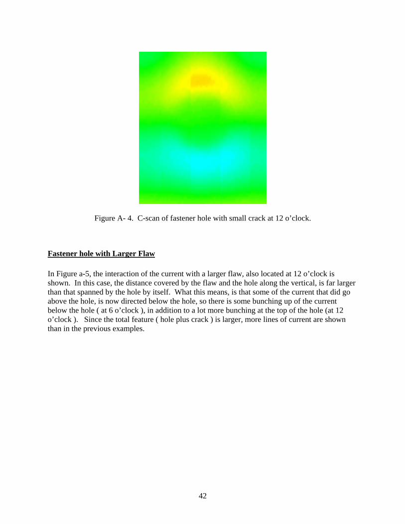
42
Figure A- 4. C-scan of fastener hole with small crack at 12 o’clock.
Fastener hole with Larger Flaw In Figure a-5, the interaction of the current with a larger flaw, also located at 12 o’clock is shown. In this case, the distance covered by the flaw and the hole along the vertical, is far larger than that spanned by the hole by itself. What this means, is that some of the current that did go above the hole, is now directed below the hole, so there is some bunching up of the current below the hole ( at 6 o’clock ), in addition to a lot more bunching at the top of the hole (at 12 o’clock ). Since the total feature ( hole plus crack ) is larger, more lines of current are shown than in the previous examples.

43
Figure A-5. Current redirected around a fastener hole with a large crack at 12 o’clock. Note that
current is bunched up some at 6 o’clock, and a lot at 12 o’clock. A C-scan taken with MR sensors of this sort of hole is shown in Figure A-6. Note that the intensity of the response is increased at both the top and bottom, but there is more at the top, and the shape of the yellow/orange region at the top is somewhat more pointed than at the bottom, as we would expect from looking at Figure A-5. In terms of dimensions, the fastener hole is approximately 3/8 inch diameter, the thickness of the upper layer is 0.350”, the thickness of the lower layer is 0.305 inch, and the length of the crack is 0.200”. The crack in the scan shown in Figure A-4 was only 0.076”, with the other dimensions being the same.
Figure A-6. C-scan of a fastener hole with a larger (0.200”) flaw at 12 o’clock.

44
In Figure a-6, the field at the top is more intense than at the bottom, although the bottom is intensified as well. The regions of intense positive and negative field are due to the bunching of the current in those regions. This effect is more exaggerated for an even larger (0.250”) crack at 12 o’clock as shown in Figure A-7.
Figure A-7. C-scan of a fastener hole with an even larger (0250”) flaw at 12 o’clock
6.3 Cracks at 3 o’clock and/or 9 o’clock If the cracks are horizontal, appearing at 3 or 9 o’clock, then we run the current vertically, and the results are the same, except the positive and negative regions of field are on the left and right, rather than on the top and bottom. This is shown in Figure A-8. There are four fastener holes in the scan, with dimensions the same as in the previous C-scans, with the crack lengths at 3 o’clock, as shown above the figure. The fastener holes with no cracks are marked “none”. 0.300” (3) none 0.200” (3) none
Figure A-8. Scan with flaws parallel to fastener row and current perpendicular to fastener row.