multi-channel control for microring weight banksbshastri/files/30_tait_oe-24-8-8895.pdf ·...
TRANSCRIPT
Multi-channel control for microringweight banks
Alexander N. Tait,∗ Thomas Ferreira de Lima, Mitchell A. Nahmias,Bhavin J. Shastri, and Paul R. Prucnal
Princeton University, Princeton, NJ 08544, USA∗[email protected]
Abstract: We demonstrate 4-channel, 2GHz weighted addition in asilicon microring filter bank. Accurate analog weight control becomes moredifficult with increasing number of channels, N, as feedback approachesbecome impractical and brute force feedforward approaches take O(2N)calibration measurements in the presence of inter-channel dependence. Weintroduce model-based calibration techniques for thermal cross-talk andcross-gain saturation, which result in a scalable O(N) calibration routine and3.8 bit feedforward weight accuracy on every channel. Practical calibrationroutines are indispensible for controlling large-scale microring systems.The effect of thermal model complexity on accuracy is discussed. Weightedaddition based on silicon microrings can apply the strengths of photonicmanufacturing, wideband information processing, and multiwavelengthnetworks towards new paradigms of ultrafast analog distributed processing.
© 2016 Optical Society of America
OCIS codes: (250.5300) Photonic integrated circuits; (070.1170) Analog optical signalprocessing; (130.7408) Wavelength filtering devices; (200.4700) Optical neural systems;(200.3050) Information processing.
References and links1. G. Roelkens, L. Liu, D. Liang, R. Jones, A. Fang, B. Koch, and J. Bowers, “III-V/silicon photonics for on-chip
and intra-chip optical interconnects,” Laser Photonics Rev. 4(6), 751–779 (2010).2. A. Mekis, S. Gloeckner, G. Masini, A. Narasimha, T. Pinguet, S. Sahni, and P. De Dobbelaere, “A grating-
coupler-enabled CMOS photonics platform,” IEEE J. Sel. Top. Quantum Electron. 17(3), 597–608 (2011).3. J. S. Orcutt, B. Moss, C. Sun, J. Leu, M. Georgas, J. Shainline, E. Zgraggen, H. Li, J. Sun, M. Weaver, S. Urosevic,
M. Popovic, R. J. Ram, and V. Stojanovic, “Open foundry platform for high-performance electronic-photonicintegration,” Opt. Express 20(11), 12222–12232 (2012).
4. Y. Vlasov, “Silicon CMOS-integrated nano-photonics for computer and data communications beyond 100G,”IEEE Commun. Mag. 50(2), s67–s72 (2012).
5. A.-J. Lim, J. Song, Q. Fang, C. Li, X. Tu, N. Duan, K. K. Chen, R.-C. Tern, and T.-Y. Liow, “Review of siliconphotonics foundry efforts,” IEEE J. Sel. Top. Quantum Electron. 20(4), 405–416 (2014).
6. P. A. Merolla, J. V. Arthur, R. Alvarez-Icaza, A. S. Cassidy, J. Sawada, F. Akopyan, B. L. Jackson, N. Imam,C. Guo, Y. Nakamura, B. Brezzo, I. Vo, S. K. Esser, R. Appuswamy, B. Taba, A. Amir, M. D. Flickner, W. P.Risk, R. Manohar, and D. S. Modha, “A million spiking-neuron integrated circuit with a scalable communicationnetwork and interface,” Science 345(6197), 668–673 (2014).
7. G. Indiveri, B. Linares-Barranco, T. J. Hamilton, A. van Schaik, R. Etienne-Cummings, T. Delbruck, S.-C. Liu,P. Dudek, P. Hfliger, S. Renaud, J. Schemmel, G. Cauwenberghs, J. Arthur, K. Hynna, F. Folowosele, S. Saighi,T. Serrano-Gotarredona, J. Wijekoon, Y. Wang, and K. Boahen, “Neuromorphic silicon neuron circuits,” Front.Neurosci. 5(73), 1–23 (2011).
8. J. Hasler and H. B. Marr, “Finding a roadmap to achieve large neuromorphic hardware systems,” Front. Neurosci.7(118), 00118 (2013).
9. P. Asthana, G. P. Nordin, J. Armand R. Tanguay, and B. K. Jenkins, “Analysis of weighted fan-out/fan-in volumeholographic optical interconnections,” Appl. Opt. 32(8), 1441–1469 (1993).
#258667 Received 1 Feb 2016; revised 3 Apr 2016; accepted 4 Apr 2016; published 14 Apr 2016 (C) 2016 OSA 18 Apr 2016 | Vol. 24, No. 8 | DOI:10.1364/OE.24.008895 | OPTICS EXPRESS 8895

10. M. Hill, E. E. E. Frietman, H. de Waardt, G.-D. Khoe, and H. Dorren, “All fiber-optic neural network usingcoupled SOA based ring lasers,” IEEE Trans. Neural Networks 13(6), 1504–1513 (2002).
11. A. N. Tait, M. A. Nahmias, B. J. Shastri, and P. R. Prucnal, “Broadcast and weight: an integrated network forscalable photonic spike processing,” J. Lightwave Technol. 32(21), 3427–3439 (2014).
12. R. Ramaswami, “Multiwavelength lightwave networks for computer communication,” IEEE Commun. Mag.31(2), 78–88 (1993).
13. D. Marpaung, C. Roeloffzen, R. Heideman, A. Leinse, S. Sales, and J. Capmany, “Integrated microwave photon-ics,” Laser Photonics Rev. 7(4), 506–538 (2013).
14. M. Chang, M. Fok, A. Hofmaier, and P. Prucnal, “Optical analog self-interference cancellation using electro-absorption modulators,” IEEE Microwave Wireless Compon. Lett. 23(2), 99–101 (2013).
15. M. A. Nahmias, B. J. Shastri, A. N. Tait, and P. R. Prucnal, “A leaky integrate-and-fire laser neuron for ultrafastcognitive computing,” IEEE J. Sel. Top. Quantum Electron. 19(5), 1800212 (2013).
16. W. Coomans, L. Gelens, S. Beri, J. Danckaert, and G. Van der Sande, “Solitary and coupled semiconductor ringlasers as optical spiking neurons,” Phys. Rev. E 84(3), 036209 (2011).
17. F. Selmi, R. Braive, G. Beaudoin, I. Sagnes, R. Kuszelewicz, and S. Barbay, “Relative refractory period in anexcitable semiconductor laser,” Phys. Rev. Lett. 112, 183902 (2014).
18. B. J. Shastri, M. A. Nahmias, A. N. Tait, A. W. Rodriguez, B. Wu, and P. R. Prucnal, “Spike processing with agraphene excitable laser,” Sci. Rep. 5, 19126 (2015).
19. A. N. Tait, M. A. Nahmias, Y. Tian, B. J. Shastri, and P. R. Prucnal, “Photonic Neuromorphic Signal Processingand Computing,” in Nanophotonic Information Physics, M. Naruse, ed., pp. 183–222 (Springer, 2014).
20. E. Klein, D. Geuzebroek, H. Kelderman, G. Sengo, N. Baker, and A. Driessen, “Reconfigurable optical add-dropmultiplexer using microring resonators,” IEEE Photonics Technol. Lett. 17(11), 2358–2360 (2005).
21. J. C. C. Mak, W. D. Sacher, T. Xue, J. C. Mikkelsen, Z. Yong, and J. K. S. Poon, “Automatic Resonance Align-ment of High-Order Microring Filters,” IEEE J. Quantum Electron. 51(11), 1–11 (2015).
22. J. A. Cox, A. L. Lentine, D. C. Trotter, and A. L. Starbuck, “Control of integrated micro-resonator wavelengthvia balanced homodyne locking,” Opt. Express 22(9), 11279–11289 (2014).
23. J. Cardenas, M. A. Foster, N. Sherwood-Droz, C. B. Poitras, H. L. R. Lira, B. Zhang, A. L. Gaeta, J. B. Khurgin,P. Morton, and M. Lipson, “Wide-bandwidth continuously tunable optical delay line using silicon microringresonators,” Opt. Express 18(25), 26,525–26,534 (2010).
24. C. T. DeRose, M. R. Watts, D. C. Trotter, D. L. Luck, G. N. Nielson, and R. W. Young, “Silicon microringmodulator with integrated heater and temperature sensor for thermal control,” in Conference on Lasers andElectro-Optics (Optical Society of America, 2010), paper CThJ3.
25. H. Jayatilleka, K. Murray, M. Angel Guillen-Torres, M. Caverley, R. Hu, N. A. F. Jaeger, L. Chrostowski, andS. Shekhar, “Wavelength tuning and stabilization of microring-based filters using silicon in-resonator photocon-ductive heaters,” Opt. Express 23(19), 25084–25097 (2015).
26. A. Tait, T. Ferreira de Lima, M. Nahmias, B. Shastri, and P. Prucnal, “Continuous calibration of microring weightsfor analog optical networks,” IEEE Photonics Technol. Lett. 28(8), 887–890 (2016).
27. A. Tait, M. Nahmias, B. Shastri, M. Chang, A. Wu, E. Zhou, E. Blow, T. Ferreira de Lima, B. Wu, and P. Prucnal,“Balanced WDM weight banks for analog optical processing and networking in silicon,” in Summer Topicals,(IEEE/OSA, 2015), paper MC2.3.
28. M. A. Nahmias, A. N. Tait, B. J. Shastri, T. F. de Lima, and P. R. Prucnal, “Excitable laser processing networknode in hybrid silicon: analysis and simulation,” Opt. Express 23(20), 26800–26813 (2015).
29. A. Tait, A. Wu, E. Zhou, T. Ferreira de Lima, M. Nahmias, B. Shastri, and P. Prucnal, “Multi-channel microringweight bank control for reconfigurable analog photonic networks,” in Optical Interconnects, (IEEE, 2016), paperWC4.
30. S. Friedmann, N. Fremaux, J. Schemmel, W. Gerstner, and K. Meier, “Reward-based learning under hardwareconstraints - using a RISC processor embedded in a neuromorphic substrate,” Front. Neurosci. 7(160) (2013).
31. F. Akopyan, J. Sawada, A. Cassidy, R. Alvarez-Icaza, J. Arthur, P. Merolla, N. Imam, Y. Nakamura, P. Datta, G.-J. Nam, B. Taba, M. Beakes, B. Brezzo, J. Kuang, R. Manohar, W. Risk, B. Jackson, and D. Modha, “TrueNorth:design and tool flow of a 65 mW 1 million neuron programmable neurosynaptic chip,” IEEE Trans. Comput.Aided Des. Integr. Circuits Syst. 34(10), 1537–1557 (2015).
32. L. Chrostowski and M. Hochberg, Silicon Photonics Design: From Devices to Systems (Cambridge UniversityPress, 2015).
33. R. J. Bojko, J. Li, L. He, T. Baehr-Jones, M. Hochberg, and Y. Aida, “Electron beam lithography writing strategiesfor low loss, high confinement silicon optical waveguides,” J. Vac. Sci. Technol., B 29(6), 06F309 (2011).
34. Y. Wang, X. Wang, J. Flueckiger, H. Yun, W. Shi, R. Bojko, N. A. Jaeger, and L. Chrostowski, “Focusing sub-wavelength grating couplers with low back reflections for rapid prototyping of silicon photonic circuits,” Opt.Express 22(17), 20652–20662 (2014).
35. A. N. Tait, J. Chang, B. J. Shastri, M. A. Nahmias, and P. R. Prucnal, “Demonstration of WDM weighted additionfor principal component analysis,” Opt. Express 23(10), 12758–12765 (2015).
36. M. S. Dahlem, C. W. Holzwarth, A. Khilo, F. X. Kartner, H. I. Smith, and E. P. Ippen, “Reconfigurable multi-channel second-order silicon microring-resonator filterbanks for on-chip WDM systems,” Opt. Express 19(1),
#258667 Received 1 Feb 2016; revised 3 Apr 2016; accepted 4 Apr 2016; published 14 Apr 2016 (C) 2016 OSA 18 Apr 2016 | Vol. 24, No. 8 | DOI:10.1364/OE.24.008895 | OPTICS EXPRESS 8896

306–316 (2011).37. H. Park, Y. hao Kuo, A. W. Fang, R. Jones, O. Cohen, M. J. Paniccia, and J. E. Bowers, “A hybrid AlGaInAs-
silicon evanescent preamplifier and photodetector,” Opt. Express 15(21), 13539–13546 (2007).38. J. D. B. Bradley and E. S. Hosseini, “Monolithic erbium- and ytterbium-doped microring lasers on silicon chips,”
Opt. Express 22(10), 12226–12237 (2014).39. P. Dong, S. Liao, D. Feng, H. Liang, D. Zheng, R. Shafiiha, C. Kung, W. Qian, G. Li, X. Zheng, A. Krish-
namoorthy, and M. Asghari, “Low Vpp, ultralow-energy, compact, high-speed silicon electro-optic modulator,”Opt. Express 17(25), 22484–22490 (2009).
40. H. Jayatilleka, K. Murray, M. Caverley, N. Jaeger, L. Chrostowski, and S. Shekhar, “Crosstalk in SOI microringresonator-based filters,” J. Lightwave Technol. PP(99), 1–1 (2015).
41. O. Schwelb, “Generalized analysis for a class of linear interferometric networks. I. Analysis,” IEEE Trans. Mi-crowave Theory Tech. 46(10), 1399–1408 (1998).
1. Introduction
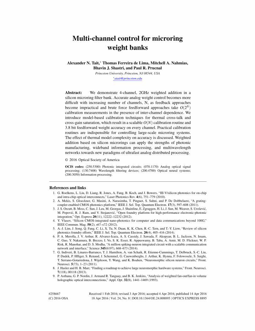
Advances in photonic integrated circuit (PIC) technologies [1–5] will generate opportunitiesfor large-scale, low-cost optical processing systems. At the same time, a revival is underwayin unconventional (neuro-inspired) microelectronic computing architectures, aimed to addressenergy efficiency limitations inherent in von Neumann computers [6–8]. Neuro-inspired hard-ware addresses these issues, in part, by distributing processing among many nodes, and, assuch, rely heavily on multi-access networking strategies in which connection strengths (i.e.“weights”) are reconfigurable. It has long been recognized that optical physics are well-suitedto the analog interconnect problem, yet solutions based on holograms [9] and fiber [10] cir-cuits have not led to integrated systems. We have previously proposed a PIC-compatible multi-access analog network called “broadcast-and-weight” [11], which combines results in mul-tiwavelength networks [12], analog photonic links [13, 14], and photonic neurons [15–18].Broadcast-and-weight networks could open processing domains with unprecedented speed andcomplexity [19]. Figure 1(a) depicts the concept of a broadcast-and-weight network.
Broadcast-and-weight relies heavily on wavelength-division multiplexed (WDM) weightedaddition. The analog network topology is “programmed” by controlling weight values. Mi-croring resonator (MRR) implementations of weight banks, drawn in Fig. 1(b), have the advan-tages of compactness, WDM capability, and ease of tuning. On the other hand, MRR sensitivityto fabrication variations, thermal fluctuations, and thermal cross-talk presents a control prob-lem. MRR control is an important topic for WDM demultiplexers [20], high-order filters [21],modulators [22], and delay lines [23]. MRR controllers are often based on online feedbackcontrol [24, 25], but the unique requirements of an analog weight bank (continuous range ofweights, input signals of unknown amplitude and shape, etc.) call for a feedforward controlapproach with offline pre-calibration performed at least once per fabricated device [26].
Prior work demonstrated feedforward control of an add/drop MRR filter edge for effect-ing a continuous range of transmission values. This enabled a single photonic weight with arange of –1 to +1 [27] and precision of 3.1 bits [26] (i.e. a maximum error of ±0.117 overthe range ±1, or a dynamic range of 9.33dB). Calibration consisted of recording weights overthe filter edge tuning range and interpolating. The results in [26] are preliminary in the sensethat interpolation-based techniques are impractical for simulataneously controlling more thanone MRR weight, an essential requirement for photonic weight banks and weighted opticalnetworks. When weight interdependency or cross-talk are present, the control problem cannot be separated into N isolated channels. The dimensionality of the full tuning range increaseswith N, necessitating O(2N) calibration measurements in general. The major contributions ofthe present work are full, simultaneous control of MRR weight banks and the development oftractable, O(N), calibration methods for banks with any number of channels.
Model-based calibration is required for the two predominant sources of weight interdepen-dency: thermal cross-talk and cross-gain saturation. In this work, we expand on preliminary
#258667 Received 1 Feb 2016; revised 3 Apr 2016; accepted 4 Apr 2016; published 14 Apr 2016 (C) 2016 OSA 18 Apr 2016 | Vol. 24, No. 8 | DOI:10.1364/OE.24.008895 | OPTICS EXPRESS 8897
IN
THRU
DROP
DROP
THRUIN
20 µm
Fig$1$
.$.$.$
.$.$.$
E/OConversion
(NL process)
λ1
λ2λ3λ4
SpectralFilter Bank(Weight)
BalancedDetector
(Add)RFlink
Weighted Addition
b)
c) d)
a)
100 µm
resonator tuningWDMinputs
RF output
IN THRU
DROP
PD+
PD–
Fig. 1. a) Role of WDM weighted addition in a proposed on-chip analog photonic process-ing network [11]. Each E/O node – which could be any nonlinear modulator, direct-drivenlaser, or dynamical laser neuron – produces a signal modulated on a unique wavelength.Weighted addition banks produce electrical signals that drive the E/O converters [28]. b)Microring resonator (MRR) implementation of a WDM weight bank. Tuning MRRs be-tween on- and off- resonance switches a continuous amount of optical power betweendrop and through ports. A balanced photodetector (PD) yields the sum and difference ofweighted signals. c) Optical micrograph of the device under test, showing a bank of fourthermally-tuned MRRs. d) Wide area micrograph, showing fiber-to-chip grating couplerports.
results in [29], developing models whose parameters can be fit (i.e. calibrated) with a O(N) rou-tine of spectral and oscilloscope measurements. Whereas an interpolation-only approach with20 points resolution would require 204 = 160,000 calibration measurements, the presented cali-bration routine takes roughly 4× [10(heater)+20(filter)+4(amplifier)] = 136 total calibrationmeasurements. We then assess factors affecting weight precision, including the complexity ofthe thermal cross-talk model. We demonstrate simultaneous 4-channel MRR weight controlwith an accuracy of 3.8 bits and precision of 4.0 bits (plus 1.0 sign bit) on each channel. Whileoptimal weight resolution is still a topic of discussion in the neuromorphic electronics commu-nity [8], several state-of-the-art architectures with dedicated weight hardware have settled on4-bit resolution [30,31]. Practical, accurate, and scalable MRR control techniques are a criticalstep towards large scale analog processing networks based on MRR weight banks.
2. Methods
MRR weight bank samples were fabricated on silicon-on-insulator wafers at the WashingtonNanofabrication Fabrication through the UBC SiEPIC rapid prototyping group [32]. Siliconthickness is 220 nm, and buried oxide thickness is 3 µm. 500 nm wide WGs were patterned byEbeam lithography and fully etched to the buried oxide [33]. A hydrogen silsesquioxane resist(HSQ, Dow-Corning XP-1541-006) was spin-coated at 4000 rpm, then hotplate baked at 80 Cfor 4 minutes. Electron beam lithography was performed using a JEOL JBX-6300FS systemoperated at 100 keV energy, 8 nA beam current, 500 µm exposure field size, and exposuredose of 2800 µC/cm2. The resist was developed by immersion in 25% tetramethylammoniumhydroxide (TMAH) for 4 minutes. Silicon was etched from unexposed areas by inductivelycoupled plasma etching in an Oxford Plasmalab System, with a chlorine gas flow of 20 sccm,pressure of 12 mT, ICP power of 800 W, bias power of 40 W, and a plate temperature of 20 ◦C,resulting in a bias voltage of 185 V. Thermo-optic MRR resonance tuning is accomplished byohmic heating of Ti/Pt/Au contacts (100 A:Ti, 50 A:Pt, 2000 A:Au), which were deposited ontop of a 3 µm oxide passivation layer using an Angstron Engineering electron beam evaporation

FBGarray
½∆T
Fig 2
MZM
DFBsPPGPRBS
AWG
EDFAsscope
DACMicroringWeightBank
PD
a) b)
c)
DROP
THRU
CPU
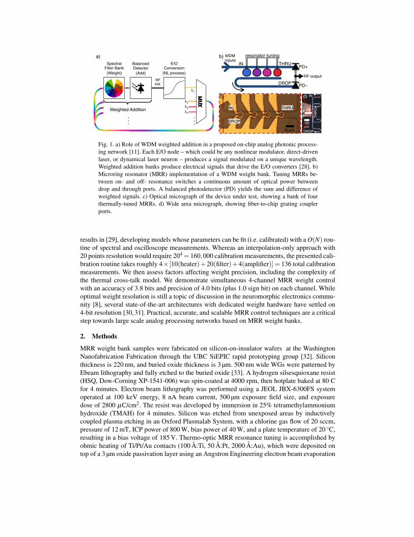
Fig. 2. a) Experimental setup. An input generator creates uncorrelated signals on differ-ent wavelengths by time delaying a single PRBS. DFB: distributed feedback laser; AWG:arrayed-waveguide grating; PPG: pulse pattern generator; MZM: Mach-Zehnder Modula-tor; FBG: fiber Bragg grating. The microring weight bank is thermally tuned by a current-mode DAC (digital-to-analog converter). Drop and thru outputs are amplified by erbiumdoped fiber amplifiers (EDFAs) and delay-matched before detection by a balanced pho-todetector (PD). A computer (CPU) executes the calibration routine. b) Time domain tracesof reference input signals on different wavelength channels. c) Optical spectrum of WDMinputs (red) and transmission spectra of the drop port when tuning current is off (gray) andtuned onto resonance (blue), measured with a drop port spectrum analyzer (not shown).
system.The weight bank device pictured in Fig. 1(c) consists of two bus waveguides and four MRRs
in a parallel add/drop configuration , each of which controls a single wavelength channel bytuning on or off resonance. The radii of the MRRs are [6.37, 6.90, 7.43, and 7.96] µm, respec-tively. Coupling region gaps were 200 nm, and neighboring MRRs are separated by 20 µm.Q-factors are approximately 10,000. The free spectral range of the first MRR is measured tobe 15 nm, indicating an effective TE refractive index of 4.2. . The sample is mounted on atemperature-controlled alignment stage and coupled to fiber with TE focusing subwavelengthgrating couplers [34].
The experimental setup shown in Fig. 2(a) consists of a multiwavelength reference inputgenerator [35] that produces statistically independent signals by imparting channel-dependentdelays on a 2Gbps pseudo-random bit sequence (PRBS). These reference signals are shownin Fig. 2(b). A 4-channel 13-bit digital-to-analog converter (DAC), NI PCI-6723, buffered toprovide up to 80 mA per channel, tunes the electrical power dissipated in each MRR heater.The heaters share a common connection to reduce electrical I/O count. Since this common wireis not perfectly conducting, the effective common voltage can fluctuate with total current flow.Current-mode drivers are used to avoid this issue. The drop and through outputs of the MRRweight bank are amplified, their net delays matched, and detected by a balanced photodiode(PD). A transmission spectrum analyzer (not shown) is also connected to the device to simul-taneously monitor the filter resonance peaks, tune them onto resonance with the WDM inputsignals , and assist in thermal model calibration. Figure 2(c) depicts tuning the bank from theinitial state to the all channels on-resonance state.
Although input signals to the MRR weight bank are not necessarily known during an op-eration phase, the calibration phase can take advantage of known reference inputs in order tosimultaneously measure the effective weight of each channel. In this case, references were de-

layed PRBS signals, each of which is stored as xi(t). If channel delays exceed one bit period,then the correlation
⟨xi(t) · x j(t)
⟩t approaches zero for a sufficiently long pattern (in this work,
27 bits). All weights µi can then be determined by decomposing a single measurement m(t) interms of stored references:
µi =〈xi(t) ·m(t)〉t〈xi(t) · xi(t)〉t
(1)
The calibration routine estimates a mapping of applied current to weight~i→~µ . The inverseof this mapping becomes the feedforward control rule for effecting a desired weight vector. Weseparate the map into physical stages for thermal tuning (~i→ ~∆λ ), MRR bank transmission( ~∆λ → ~T ), and actual detected weight (~T →~µ).
2.1. Thermal cross-talk model
The temperature of an MRR waveguide is affected predominantly by the heater directly above,but heat can also leak between nearby MRRs. The relationship between dissipated electricalpower, ~i2R, and resonant wavelength shift, ~λ −~λ0 is linear and can be modeled by a matrix,KKK [36]. Assuming heater resistance is constant,
~λ −~λ0 = KKK~i2 (2)
where λ0 is the resonant wavelength at zero tuning current, and KKK is a nearly diagonal ma-trix that describes the thermo-optic effect, heat transfer coupling, and heater resistance. Off-diagonals of KKK decribe unintended heat transfer from a given heater to filter of different chan-nels, a.k.a. thermal cross-talk. Substituting q j ≡ i2j for notational clarity, this equation can be
put in a differential form around WDM signal wavelengths, ~λsig, and the tuning current neededto bias filters on-resonance with these signals, ~qbias,
~λsig−~λ0 = KKK~qbias (3)~λ −~λsig = KKK (~q−~qbias) (4)
~∆λ = KKK ~∆q (5)
This linear model is simple to calibrate and invert, but it relies on an assumption of constantheater resistance. In general, heater resistance is also temperature dependent due to thermo-electric self-heating. For a single current-driven heater with ambient resistance of R0 andthermo-electric coefficient α ,
R(q) = R0 [1+αqR(q)] (6)
=R0
1−αR0q(7)
which is certainly not constant, and even has a singularity at q = (αR0)−1, signifying a thermal
runaway. Instead of combining the multivariate and nonlinear equations above, we simply notethat non-constant resistance means that second and higher-order derivatives of ~∆λ in terms of~∆q are non-zero but small enough that a Taylor expansion can incorporate the nonlinearities.
~∆λ ≈D
∑d=1
KKKddd ~∆qd
(8)
where D is model order, the exponentiation of ~∆q is element-wise, and the model now containsD distinct KKK matrices.
#258667 Received 1 Feb 2016; revised 3 Apr 2016; accepted 4 Apr 2016; published 14 Apr 2016 (C) 2016 OSA 18 Apr 2016 | Vol. 24, No. 8 | DOI:10.1364/OE.24.008895 | OPTICS EXPRESS 8900
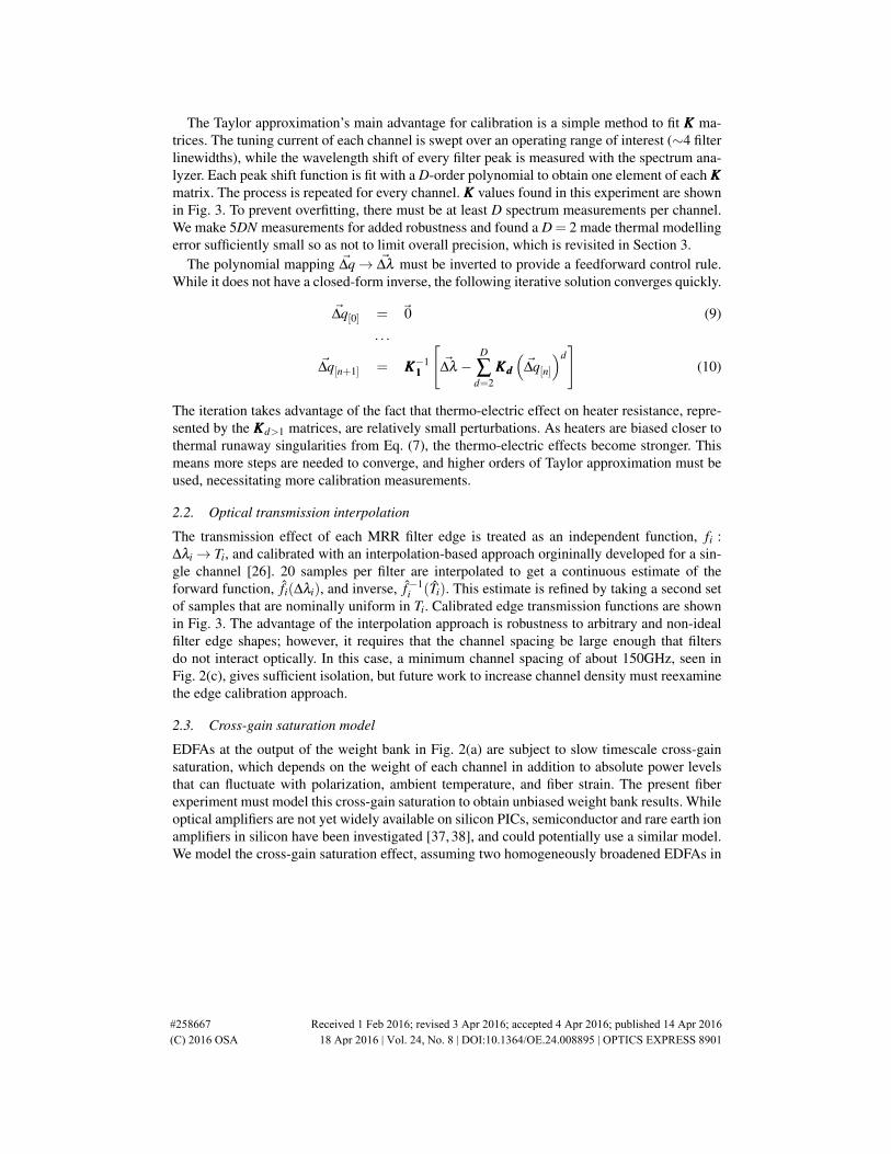
The Taylor approximation’s main advantage for calibration is a simple method to fit KKK ma-trices. The tuning current of each channel is swept over an operating range of interest (∼4 filterlinewidths), while the wavelength shift of every filter peak is measured with the spectrum ana-lyzer. Each peak shift function is fit with a D-order polynomial to obtain one element of each KKKmatrix. The process is repeated for every channel. KKK values found in this experiment are shownin Fig. 3. To prevent overfitting, there must be at least D spectrum measurements per channel.We make 5DN measurements for added robustness and found a D = 2 made thermal modellingerror sufficiently small so as not to limit overall precision, which is revisited in Section 3.
The polynomial mapping ~∆q→ ~∆λ must be inverted to provide a feedforward control rule.While it does not have a closed-form inverse, the following iterative solution converges quickly.
~∆q[0] = ~0 (9). . .
~∆q[n+1] = KKK−1111
[~∆λ −
D
∑d=2
KKKddd
(~∆q[n]
)d]
(10)
The iteration takes advantage of the fact that thermo-electric effect on heater resistance, repre-sented by the KKKd>1 matrices, are relatively small perturbations. As heaters are biased closer tothermal runaway singularities from Eq. (7), the thermo-electric effects become stronger. Thismeans more steps are needed to converge, and higher orders of Taylor approximation must beused, necessitating more calibration measurements.
2.2. Optical transmission interpolation
The transmission effect of each MRR filter edge is treated as an independent function, fi :∆λi→ Ti, and calibrated with an interpolation-based approach orgininally developed for a sin-gle channel [26]. 20 samples per filter are interpolated to get a continuous estimate of theforward function, fi(∆λi), and inverse, f−1
i (Ti). This estimate is refined by taking a second setof samples that are nominally uniform in Ti. Calibrated edge transmission functions are shownin Fig. 3. The advantage of the interpolation approach is robustness to arbitrary and non-idealfilter edge shapes; however, it requires that the channel spacing be large enough that filtersdo not interact optically. In this case, a minimum channel spacing of about 150GHz, seen inFig. 2(c), gives sufficient isolation, but future work to increase channel density must reexaminethe edge calibration approach.
2.3. Cross-gain saturation model
EDFAs at the output of the weight bank in Fig. 2(a) are subject to slow timescale cross-gainsaturation, which depends on the weight of each channel in addition to absolute power levelsthat can fluctuate with polarization, ambient temperature, and fiber strain. The present fiberexperiment must model this cross-gain saturation to obtain unbiased weight bank results. Whileoptical amplifiers are not yet widely available on silicon PICs, semiconductor and rare earth ionamplifiers in silicon have been investigated [37, 38], and could potentially use a similar model.We model the cross-gain saturation effect, assuming two homogeneously broadened EDFAs in
#258667 Received 1 Feb 2016; revised 3 Apr 2016; accepted 4 Apr 2016; published 14 Apr 2016 (C) 2016 OSA 18 Apr 2016 | Vol. 24, No. 8 | DOI:10.1364/OE.24.008895 | OPTICS EXPRESS 8901
0 0.20
1
0 0.20
1
0 0.20
1
0 0.20
1
nm$
0 0.20
1
0 0.20
1
0 0.20
1
0 0.20
1
0 0.20
1
0 0.20
1
0 0.20
1
0 0.20
1
0 0.20
1
0 0.20
1
0 0.20
1
0 0.20
1
∆q ∆λ T µEq. 7 Eq. 14K1 (x100)
7.38 0.02 0.06 0.120.18 10.5 0.04 0.410.14 0.63 7.52 0.050.07 0.04 0.22 5.91
Heater Filter Amplifier λsig,1 : 1547nm qbias,1 : (51.8mA)2
λsig,2 : 1549nm qbias,2 : (49.0mA)2
λsig,3 : 1550nm qbias,3 : (39.9mA)2
λsig,4 : 1552nm qbias,4 : (11.5mA)2
iBias
K2 (x1,000)0.03 0.85 0.77 0.081.54 -3.13 -1.10 -0.230.24 1.39 -1.29 -0.390.07 -0.19 -0.32 -2.52
Pos. Amp.B+ C+
1.23 0.0062.53 0.1892.67 0.0422.04 0.021
Neg. Amp.B– C–
2.89 0.0568.93 0.0816.92 0.1144.52 0.093
f1
f2
f3
f4
Fig. 3. Diagram of modelling stages showing calibrated parameter values fit during this ex-periment. Bias stage puts variables in differential form around the state of all filters beingon-resonance with signals, ~λsig. Heater stage models thermo-electric, heat transfer, andthermo-optic effects with a predominantly diagonal, linear KKK111 matrix and nonlinear cor-rections (order D = 2 shown). Filter stage consists of four independent interpolation-basedestimates of the transmission along each MRR filter edge. Amplifier stage models absoluteoptical powers and fiber amplifier saturation characteristics preceding photodetection.
non-depleted pump regimes, as
µi = Pin,iTc,i
Tig+i,ss
1+ P+ampP+
s
− γi(1−Ti)g−i,ss
1+ P−amp
P−s
(11)
P+amp = ∑
jPin, jTc, jTj (12)
P−amp = ∑j
Pin, jTc, jγ j(1−Tj) (13)
where i indicates channel number and T is the tunable microring through port transmission. Pinis input power, Tc is net coupling efficiency, γ is drop efficiency, gss is amplifier small-signalgain, and Ps is saturation power, which is not channel-dependent. Pamp signifies total powerincident on an EDFA. (+,–) superscripts respectively indicate the amplifiers on through anddrop output ports. Not all physical parameters are observable from weight measurements, butthe following parameterization yields a fittable model:
µi =B+
i
1+∑ j C+j Tj
Ti−B−i
1+∑ j C−j (1−Tj)
(1−Ti) (14)
The parameter vectors ~B(+,−) and ~C(+,−) (totaling 4N parameters) can be fit (i.e. calibrated)with a series of 4N measurements at particular tuning states. We introduce a notation µ
(xy)i to
signify the measured weight of channel i when the transmission of channel Tj=i is x and thetransmission of other channels Tj 6=i are y. For example, µ
(10)2 signifies the weight of channel 2
when it is transmitted to the through port (T = 1) and channels 1, 3, and 4 are coupled to thedrop port (T = 0). The calibration procedure starts by measuring µ
(11)i and µ
(10)i :
µ(11)i =
B+i
1+∑ j C+j
µ(10)i =
B+i
1+C+i
(15)
#258667 Received 1 Feb 2016; revised 3 Apr 2016; accepted 4 Apr 2016; published 14 Apr 2016 (C) 2016 OSA 18 Apr 2016 | Vol. 24, No. 8 | DOI:10.1364/OE.24.008895 | OPTICS EXPRESS 8902

Channel 1 weight-1 -0.5 0 0.5 1
Cha
nnel
2 w
eigh
t
-1
-0.5
0
0.5
1a) � � �
� � �
� �
� � �
� � �
� �
b)
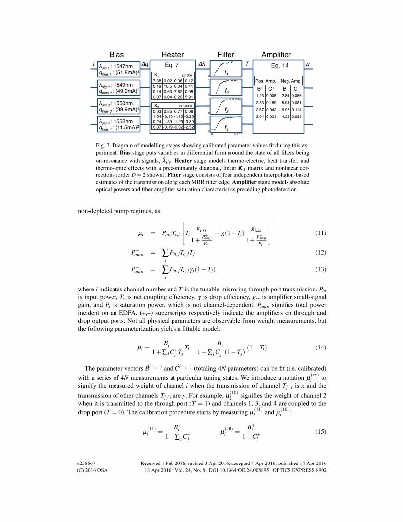
Fig. 4. a) Two-dimensional weight sweep showing controller accuracy and precision. Afterthe calibration procedure, the target weight is swept 5 times over a grid of values from –1to 1 (black grid). Black points are measured weight data. Red lines show the mean offsetfrom each target grid point. Blue ellipses indicate one standard deviation around the mean.Mean error magnitude is less than 0.072 over the span. Standard deviation remains below0.063, with a tendency to be larger for negative weights. From this plot, we estimate that theweight can be controlled with an accuracy of 3.8bits. b) Measured traces of 2Gbps signals.[ 1©- 9©] Output signals corresponding to points labeled in (a). The expected signal is in red,while measured traces are in blue. All time and voltage axes have identical scales.
These equations containing 2N unknown parameters and 2N known measurements can besolved analytically as follows.
µ(11)i
µ(10)i
=1+C+
i
1+∑ j C+j
(16)
C+i =
µ(11)i
µ(10)i
(1+∑
jC+
j
)−1 (17)
By summing this equation over all i and rearranging, the sum of C+ can be stated entirely interms of measured weights,
∑i
C+i =
N−∑ jµ(11)j
µ(10)j
∑ jµ(11)j
µ(10)j
−1(18)
at which point it can be substituted into Eq. (17) to recover individual C+ parameters. The B+
parameters then fall trivially from Eq. (15). Drop port amplifier parameters, C− and B−, fol-low an identical procedure upon measuring µ
(00)i and µ
(01)i . The ability to decompose single
measurements of m(t) into all weights via Eq. (1) means that ~µ(11) and ~µ(00) only require onemeasurement each, while the dissimilar measurements call for distinct tuning states and there-fore N measurements per amplifier. In this derivation, it was assumed that complete switchingdown to T = 0 is possible, which is not always the case in practice. A more algebraically com-plex calibration technique with nonzero Tmin can be derived similarly, but is omitted here in theinterest of space. Calibrated parameter values found for this experiment are shown in Fig. 3.
#258667 Received 1 Feb 2016; revised 3 Apr 2016; accepted 4 Apr 2016; published 14 Apr 2016 (C) 2016 OSA 18 Apr 2016 | Vol. 24, No. 8 | DOI:10.1364/OE.24.008895 | OPTICS EXPRESS 8903

Once the forward model parameters have been calibrated, we must invert the mapping ~T →~µ , Eq. (14), in order to work as a feedforward controller rule.
µi +B−i
1+∑ j C−j (1−Tj)
=B+
i
1+∑ j C+j Tj
Ti +B−i
1+∑ j C−j (1−Tj)
Ti (19)
Ti =
µi +B−i
1+∑ j C−j (1−Tj)B+
i1+∑ j C+
j Tj+
B−i1+∑ j C−j (1−Tj)
(20)
This is solved iteratively as follows:
Ti[0] = 1 (21). . .
Ti[n+1] =
µi +B−i
1+∑ j C−j (1−Tj[n])B+
i1+∑ j C+
j Tj[n]+
B−i1+∑ j C−j (1−Tj[n])
(22)
This iteration converges quickly when C parameters are small, as in Fig. 3, which is the casewhen signal powers are less than amplifier saturation power.
3. Results
After the above calibration procedure is performed, the four-dimensional command weight isswept in two-dimensions at a time while the actual weight is recorded. A sweep of commandweight values over two channels is shown in Fig. 4. Sweeps over other pairs of channels (notshown) were seen to produce similar results. Figure 4(b) shows time traces compared to expec-tation at several weight values. Traces 2 and 6 represent the original inputs and traces 8 and 4their respective inverses. The sweep in Fig. 4(a) is used to analyze accuracy, a.k.a. mean erroror repeatable error (red lines), and precision, a.k.a. dynamic error or non-repeatable error (blueellipses). Mean error is less than 0.072 over the range, corresponding to a weight accuracy of3.8 bits (i.e. 11.4dB dynamic range), and dynamic error is less than 0.062 for a weight preci-sion of 4.0 bits. Accuracy is 0.7 bits higher than in prior work with a single channel [26] due toprocedure and setup changes that minimize polarization drift.
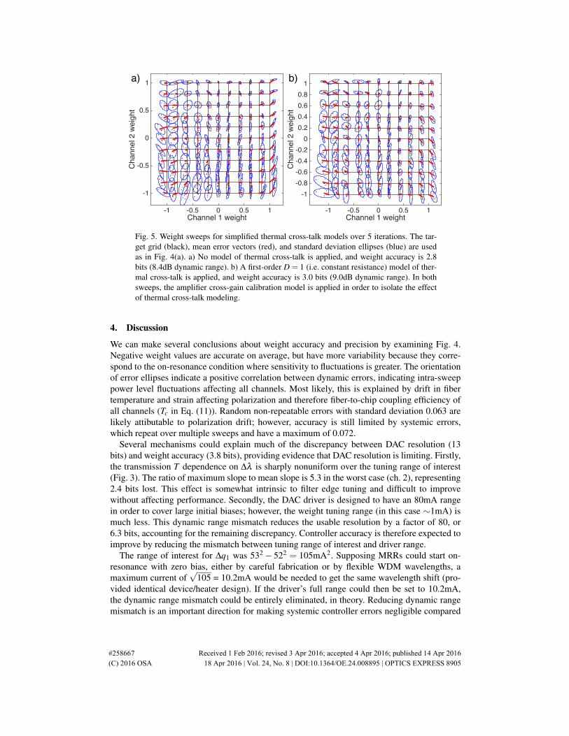
The effects of using simplified models for thermal physics are shown in Fig. 5. When thermalcross-talk and self heating are completely neglected (i.e. D = 1 and K1 is diagonal), accuracyis reduced to 2.8 bits. A constant resistance model (i.e. D = 1) is used for Fig. 5(b), yieldinga small improvement to 3.0 bits. In both cases, mean errors in Fig. 5 show no clear trend,besides being less accurate towards more negative weight values. Surprisingly, introducing alinear cross-talk model barely improves weight accuracy. This can be explained by the sharpsensitivity of filter transmission to resonant wavelength. The sensitive response of the MRRfilter edge necessitates very accurate thermal modelling, in this case, D = 2 provided significantimprovement. For the devices in this paper, we found D = 3 to yield negligible improvementover D = 2 since other factors limited precision; however, MRR weight banks with differentbiases, heater designs, materials, etc. may need increased Taylor orders for sufficient thermalmodel accuracy. An alternative to thermal tuning is depletion modulation [39], which couldeliminate thermal cross-talk and the current-squared dependence, yet requires a more involvedfabrication process with a partial etch of the top silicon layer and four dopant levels.
#258667 Received 1 Feb 2016; revised 3 Apr 2016; accepted 4 Apr 2016; published 14 Apr 2016 (C) 2016 OSA 18 Apr 2016 | Vol. 24, No. 8 | DOI:10.1364/OE.24.008895 | OPTICS EXPRESS 8904
Channel 1 weight-1 -0.5 0 0.5 1
Cha
nnel
2 w
eigh
t
-1-0.8-0.6-0.4-0.2
00.20.40.60.8
1
Channel 1 weight-1 -0.5 0 0.5 1
Cha
nnel
2 w
eigh
t
-1
-0.5
0
0.5
1
No$modeling$Linear$modeling$
a) b)
Fig. 5. Weight sweeps for simplified thermal cross-talk models over 5 iterations. The tar-get grid (black), mean error vectors (red), and standard deviation ellipses (blue) are usedas in Fig. 4(a). a) No model of thermal cross-talk is applied, and weight accuracy is 2.8bits (8.4dB dynamic range). b) A first-order D = 1 (i.e. constant resistance) model of ther-mal cross-talk is applied, and weight accuracy is 3.0 bits (9.0dB dynamic range). In bothsweeps, the amplifier cross-gain calibration model is applied in order to isolate the effectof thermal cross-talk modeling.
4. Discussion
We can make several conclusions about weight accuracy and precision by examining Fig. 4.Negative weight values are accurate on average, but have more variability because they corre-spond to the on-resonance condition where sensitivity to fluctuations is greater. The orientationof error ellipses indicate a positive correlation between dynamic errors, indicating intra-sweeppower level fluctuations affecting all channels. Most likely, this is explained by drift in fibertemperature and strain affecting polarization and therefore fiber-to-chip coupling efficiency ofall channels (Tc in Eq. (11)). Random non-repeatable errors with standard deviation 0.063 arelikely attibutable to polarization drift; however, accuracy is still limited by systemic errors,which repeat over multiple sweeps and have a maximum of 0.072.
Several mechanisms could explain much of the discrepancy between DAC resolution (13bits) and weight accuracy (3.8 bits), providing evidence that DAC resolution is limiting. Firstly,the transmission T dependence on ∆λ is sharply nonuniform over the tuning range of interest(Fig. 3). The ratio of maximum slope to mean slope is 5.3 in the worst case (ch. 2), representing2.4 bits lost. This effect is somewhat intrinsic to filter edge tuning and difficult to improvewithout affecting performance. Secondly, the DAC driver is designed to have an 80mA rangein order to cover large initial biases; however, the weight tuning range (in this case ∼1mA) ismuch less. This dynamic range mismatch reduces the usable resolution by a factor of 80, or6.3 bits, accounting for the remaining discrepancy. Controller accuracy is therefore expected toimprove by reducing the mismatch between tuning range of interest and driver range.
The range of interest for ∆q1 was 532− 522 = 105mA2. Supposing MRRs could start on-resonance with zero bias, either by careful fabrication or by flexible WDM wavelengths, amaximum current of
√105 = 10.2mA would be needed to get the same wavelength shift (pro-
vided identical device/heater design). If the driver’s full range could then be set to 10.2mA,the dynamic range mismatch could be entirely eliminated, in theory. Reducing dynamic rangemismatch is an important direction for making systemic controller errors negligible compared
#258667 Received 1 Feb 2016; revised 3 Apr 2016; accepted 4 Apr 2016; published 14 Apr 2016 (C) 2016 OSA 18 Apr 2016 | Vol. 24, No. 8 | DOI:10.1364/OE.24.008895 | OPTICS EXPRESS 8905

with dynamic errors, and also reducing the DAC resolution needed to achieve a given accuracy.A natural question to ask of MRR weight banks is minimum channel spacing. Just as the in-
troduction of thermal cross-talk dictated a switch from interpolation-based calibration to model-based calibration, weight banks with dense channel spacing will be subject to optical cross-talk,requiring optical transmission modeling. The weight bank cannot be broken into N independentmodels or interpolated functions. Since all filters couple into the same output ports, a channelthat partially couples through the “wrong” filter can still end up at the intended output, unlikein the case of a demultiplexer wherein unavoidable cross-talk dictates minimum channel spac-ing [40]. This suggests that model-based calibration of optical cross-talk in a MRR weight bankcould be instrumental for increasing channel density and number. Further work in this directionwill likely benefit from generalized models of waveguide circuits, such as described in [41].
5. Conclusion
We have demonstrated simultaneous feedforward control of a 4-channel microring weight bank,which could play a major role in large scale processing networks on silicon photonic platforms.The primary enablers of this result were scalable calibration models of thermal cross-talk andamplifier cross-gain saturation. A weight accuracy of 3.8 bits was demonstrated, on par withcorresponding state-of-the-art digital electronic neuromorphic hardware [31]. Thermal modelsthat neglect cross-talk and thermo-electric self-heating were found to be insufficient, reducingthis accuracy by 1.0 and 0.8 bits, respectively. Parameterized calibration models for opticalcross-talk could be developed for more advanced weight bank controllers. Further work couldexplore the limits of channel density in a single MRR weight bank, and the integration ofmultiple weight banks into a broadcast-and-weight network.
Acknowledgment
This work supported by the National Science Foundation (NSF) Grant No. (ECCS 1247298)and the NSF Graduate Research Fellowship Program under Grant No. (DGE 1148900). Fab-rication support was provided via the Natural Sciences and Engineering Research Council ofCanada (NSERC) Silicon Electronic-Photonic Integrated Circuits (SiEPIC) Program. Deviceswere fabricated by Richard Bojko at the University of Washington Washington NanofabricationFacility, part of the NSF National Nanotechnology Infrastructure Network (NNIN).
#258667 Received 1 Feb 2016; revised 3 Apr 2016; accepted 4 Apr 2016; published 14 Apr 2016 (C) 2016 OSA 18 Apr 2016 | Vol. 24, No. 8 | DOI:10.1364/OE.24.008895 | OPTICS EXPRESS 8906