msp430 teaching materials - utm.mxhugo/micros/capitulo6micros.pdf · •registros del...
TRANSCRIPT
03/12/2012
1
UBI
>> Contents
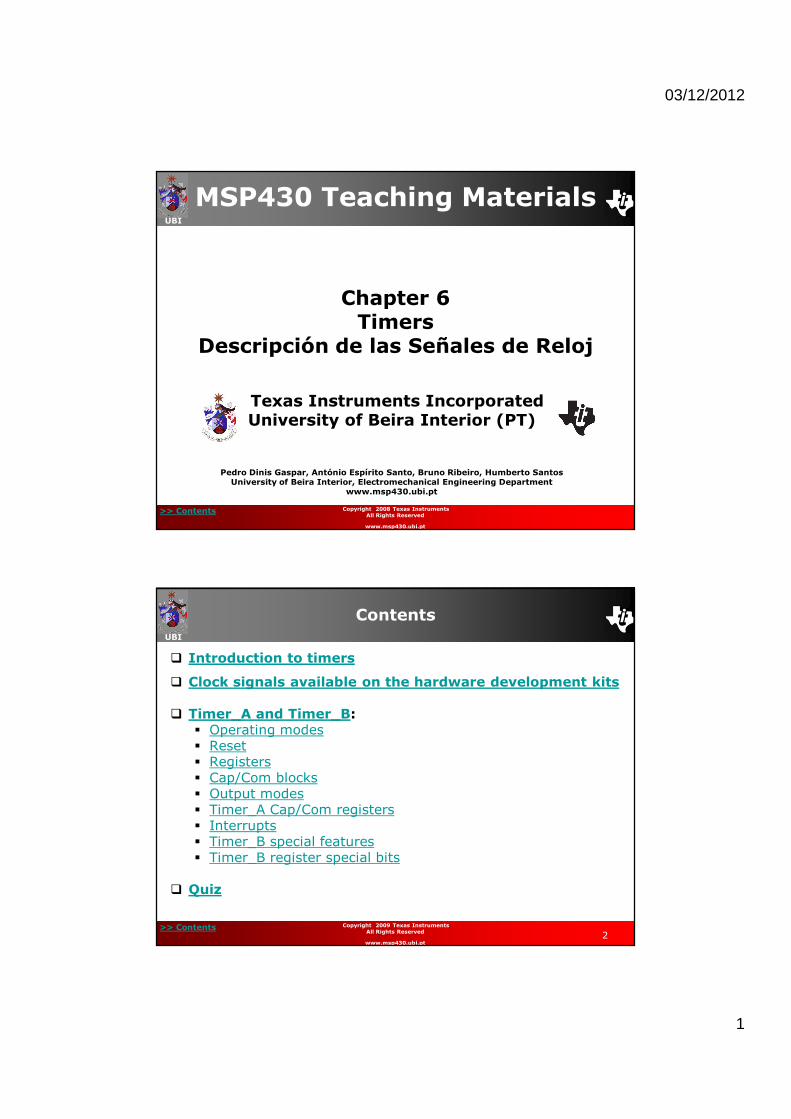
Chapter 6Timers
Descripción de las Señales de Reloj
MSP430 Teaching Materials
Texas Instruments IncorporatedUniversity of Beira Interior (PT)
Pedro Dinis Gaspar, António Espírito Santo, Bruno Ribeiro, Humberto SantosUniversity of Beira Interior, Electromechanical Engineering Department
www.msp430.ubi.pt
Copyright 2008 Texas Instruments All Rights Reserved
www.msp430.ubi.pt
UBI
>> Contents2
Copyright 2009 Texas Instruments All Rights Reserved
www.msp430.ubi.pt
Contents
� Introduction to timers
� Clock signals available on the hardware development kits
� Timer_A and Timer_B:� Operating modes� Reset� Registers� Cap/Com blocks� Output modes� Timer_A Cap/Com registers� Interrupts� Timer_B special features� Timer_B register special bits
� Quiz

03/12/2012
2
UBI
>> Contents3
Copyright 2009 Texas Instruments All Rights Reserved
www.msp430.ubi.pt
Introduction (1/3)
� La correcta temporización es un requisito fundamental para la apropiada operación de aplicaciones de tiempo real;
� Si la temporización es incorrecta, los datos de entrada podría ser procesada después de que la salida fue actualizada:
� La implementación del reloj varia entre los diferentes dispositivos en la familia del MSP430;
� Cada uno de las los dispositivos proveen diferentes fuentes de reloj, controles y usos;
UBI
>> Contents4
Copyright 2009 Texas Instruments All Rights Reserved
www.msp430.ubi.pt
Introduction (2/3)
� Familia MSP430x4xx:� Dos timers contadores de propósito general de 16-bit o 8-bit: Timer_A, Timer_B;
� Timer 1 básico (MSP430x4xx dispositivos).
� Familia MSP430x2xx:� También tiene el Timer_A y Timer_B, como el anterior;� Módulo de Reloj Básico+.
� El temporizador puede ser actualizado por el reloj interno o externo;
� El Timer_A y Timer_B también incluyen varios bloques de comparación y captura, con capacidad de interrupción;
� Los bloques de captura y comparación son usados para aplicaciones tales como:� Eventos de tiempo;� Pulse Width Modulator (PWM).

03/12/2012
3
UBI
>> Contents5
Copyright 2009 Texas Instruments All Rights Reserved
www.msp430.ubi.pt
Introduction (3/3)
� La sincronización del sistema es fundamental para casi todas las aplicaciones empotradas (embedded);
� La principal aplicación para temporizadores son:
• Generar eventos con un periodo de tiempo fijo;
• Permite una despertar periódico cuando el dispositivo esta dormido;
• Cuenta los filos de las señales en transición;
• Reemplaza lazos de retardo con llamadas a time, lo que permite al CPU dormirse entre operaciones, esto reduce el consumo de energía.
UBI
>> Contents6
Copyright 2009 Texas Instruments All Rights Reserved
www.msp430.ubi.pt
Timer_A and Timer_B Introduction (1/6)
� Timer A y B son dos timer/contadores de propósito general:
� Hay pequeñas diferencias entre los dos temporizadores;
� Las características comunes a ambos temporizadores incluyen:
� Timer/Contador asíncrono de 16-bit con cuatro modos de operación:
• Lóngituid del Timer_A: 16 bits;
• Lóngitud del Timer_B programable: 8, 10, 12, o 16 bits.
• Registro del Timer/counter, TAR (Timer_A) o TBR (Timer_B) – a partir de ahora se decribe como TxR- se incrementa o decrementa (dependiendo del modo de operación) con los filos de subida de la señal de reloj;
• El timer puede generar una interrupción cuando se desborda;
• Amplio intervalo de interrupción: 1/MCLK a 32 seg.
03/12/2012
4
UBI
>> Contents7
Copyright 2009 Texas Instruments All Rights Reserved
www.msp430.ubi.pt
Timer_A and Timer_B Introduction (2/6)
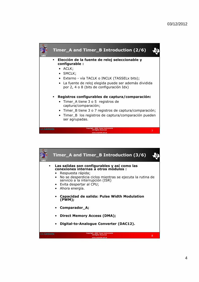
� Elección de la fuente de reloj seleccionable y configurable :
• ACLK;
• SMCLK;
• Externo - vía TACLK o INCLK (TASSELx bits);
• La fuente de reloj elegida puede ser además dividida por 2, 4 o 8 (bits de configuración Idx)
� Registros configurables de captura/comparación:
• Timer_A tiene 3 o 5 registros de captura/comparación;
• Timer_B tiene 3 o 7 registros de captura/comparación;
• Timer_B los registros de captura/comparación pueden ser agrupadas.
UBI
>> Contents8
Copyright 2009 Texas Instruments All Rights Reserved
www.msp430.ubi.pt
Timer_A and Timer_B Introduction (3/6)
� Las salidas son configurables y así como las conexiones internas a otros módulos :• Respuesta rápida; • No se desperdicia ciclos mientras se ejecuta la rutina de servicio a la interrupción (ISR)
• Evita despertar al CPU;• Ahora energía.
• Capacidad de salida: Pulse Width Modulation(PWM);
• Comparador_A;
• Direct Memory Access (DMA);
• Digital-to-Analogue Converter (DAC12).

03/12/2012
5
UBI
>> Contents9
Copyright 2009 Texas Instruments All Rights Reserved
www.msp430.ubi.pt
Timer_A and Timer_B Introduction (4/6)
� Captra asíncrona de entradas y salidas:
• Registros del Timer_A Capture/Compare (Cap/Com) no son almacenadas, son actualizadas inmediatamente cuando se le escribe;
• Registros Timer_B Cap/Com son almacenadas con sincronización y carga.
� Registro del vector de interrupciones para una decodificación rápida de la interrupción del Timer_A y Timer_B:
• TACCR0 (o TBCCR0) vector de interrupciones para TACCR0 (o TBCCCR0) CCIFG;
• TAIV (o TBIV) vector de interrupciones para la banderas remanentes CCIFG y TAIFG (o TBIFG).
UBI
>> Contents10
Copyright 2009 Texas Instruments All Rights Reserved
www.msp430.ubi.pt
Timer_A and Timer_B Introduction (5/6)
� Block diagram (Timer_A):
03/12/2012
6
UBI
>> Contents11
Copyright 2009 Texas Instruments All Rights Reserved
www.msp430.ubi.pt
Timer_A and Timer_B Introduction (6/6)
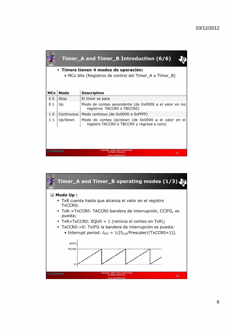
� Timers tienen 4 modos de operación:
• MCx bits (Registros de control del Timer_A o Timer_B)
MCx Mode Description
0 0 Stop El timer se para
0 1 Up Modo de conteo ascendente (de 0x0000 a el valor en losregistros TACCR0 o TBCCR0)
1 0 Continuous Modo continuo (de 0x0000 a 0xFFFF)
1 1 Up/down Modo de conteo Up/down (de 0x0000 a el valor en elregistro TACCR0 o TBCCR0 y regresa a cero)
UBI
>> Contents12
Copyright 2009 Texas Instruments All Rights Reserved
www.msp430.ubi.pt
Timer_A and Timer_B operating modes (1/3)
� Modo Up :
� TxR cuenta hasta que alcanza el valor en el registro TxCCR0;
� TxR->TxCCR0: TACCR0 bandera de interrupción, CCIFG, es puesta;
� TxR=TxCCR0: EQU0 = 1 (reinicia el conteo en TxR);
� TxCCR0->0: TxIFG la bandera de interrupción es puesta:
• Interrupt period: tINT = 1/[fCLK/Prescaler/(TxCCR0+1)].

03/12/2012
7
UBI
>> Contents13
Copyright 2009 Texas Instruments All Rights Reserved
www.msp430.ubi.pt
Timer_A and Timer_B operating modes (2/3)
� Modo Continuous:
� TxR cuienta hasta que el alcanza 0xFFFF (65536 cuentas);
� TxR=0xFFFF: TxR cuenta de cero (en el siguiente pulso de reloj);
� 0xFFFF->0: TxIFG se pone la bandera de interrupción:
• Periodo de interrupción: tINT = 1/[fCLK/Prescaler/65536];
� (Valido para TAR; para TBR 4 ver User’s Guide).
UBI
>> Contents14
Copyright 2009 Texas Instruments All Rights Reserved
www.msp430.ubi.pt
Timer_A and Timer_B operating modes (3/3)
� Up/down mode:
� TxR counts up till it reaches the value in the TxCCR0 register;
� TxCCR0-1 -> TxCCR0: Interrupt flag, CCIFG, is set;
� TxR=TxCCR0: Counting is inverted;
� 0x0001->0x0000: Interrupt flag TxIFG is set:
• Interrupt period: tINT = 1/[fCLK/Prescaler/(TxCCR0×2];
03/12/2012
8
UBI
>> Contents15
Copyright 2009 Texas Instruments All Rights Reserved
www.msp430.ubi.pt
Timer_A and Timer_B reset
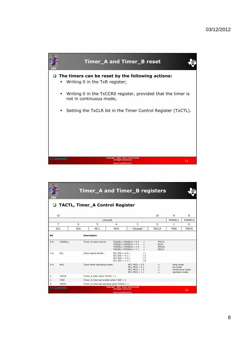
� The timers can be reset by the following actions:
� Writing 0 in the TxR register;
� Writing 0 in the TxCCR0 register, provided that the timer is not in continuous mode;
� Setting the TxCLR bit in the Timer Control Register (TxCTL).
UBI
>> Contents16
Copyright 2009 Texas Instruments All Rights Reserved
www.msp430.ubi.pt
Timer_A and Timer_B registers
� TACTL, Timer_A Control Register
15 10 9 8
Unused TASSEL1 TASSEL0
7 6 5 4 3 2 1 0
ID1 ID0 MC1 MC0 Unused TACLR TAIE TAIFG
Bit Description
9-8 TASSELx Timer_A clock source: TASSEL1 TASSEL0 = 0 0 ⇒ TACLKTASSEL1 TASSEL0 = 0 1 ⇒ ACLKTASSEL1 TASSEL0 = 1 0 ⇒ SMCLKTASSEL1 TASSEL0 = 1 1 ⇒ INCLK
7-6 IDx Clock signal divider: ID1 ID0 = 0 0⇒ / 1ID1 ID0 = 0 1⇒ / 2ID1 ID0 = 1 0⇒ / 4ID1 ID0 = 1 1⇒ / 8
5-4 MCx Clock timer operating mode: MC1 MC0 = 0 0 ⇒ Stop modeMC1 MC0 = 0 1 ⇒ Up modeMC1 MC0 = 1 0 ⇒ Continuous modeMC1 MC0 = 1 1 ⇒ Up/down mode
2 TACLR Timer_A clear when TACLR = 1
1 TAIE Timer_A interrupt enable when TAIE = 1
0 TAIFG Timer_A interrupt pending when TAIFG = 1
03/12/2012
9
UBI
>> Contents
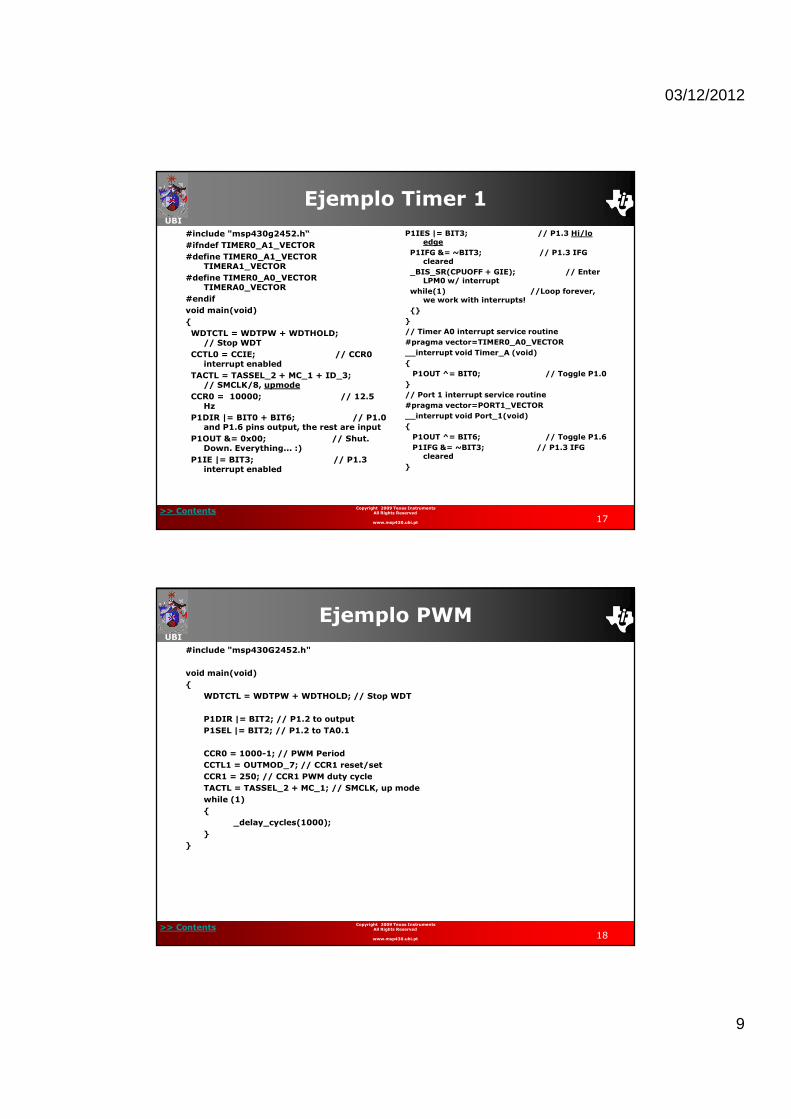
Ejemplo Timer 1
#include "msp430g2452.h“
#ifndef TIMER0_A1_VECTOR
#define TIMER0_A1_VECTOR TIMERA1_VECTOR
#define TIMER0_A0_VECTOR TIMERA0_VECTOR
#endif
void main(void)
{
WDTCTL = WDTPW + WDTHOLD; // Stop WDT
CCTL0 = CCIE; // CCR0 interrupt enabled
TACTL = TASSEL_2 + MC_1 + ID_3; // SMCLK/8, upmode
CCR0 = 10000; // 12.5 Hz
P1DIR |= BIT0 + BIT6; // P1.0 and P1.6 pins output, the rest are input
P1OUT &= 0x00; // Shut. Down. Everything... :)
P1IE |= BIT3; // P1.3 interrupt enabled
P1IES |= BIT3; // P1.3 Hi/lo edge
P1IFG &= ~BIT3; // P1.3 IFG cleared
_BIS_SR(CPUOFF + GIE); // Enter LPM0 w/ interrupt
while(1) //Loop forever, we work with interrupts!
{}
}
// Timer A0 interrupt service routine
#pragma vector=TIMER0_A0_VECTOR
__interrupt void Timer_A (void)
{
P1OUT ^= BIT0; // Toggle P1.0
}
// Port 1 interrupt service routine
#pragma vector=PORT1_VECTOR
__interrupt void Port_1(void)
{
P1OUT ^= BIT6; // Toggle P1.6
P1IFG &= ~BIT3; // P1.3 IFG cleared
}
17
Copyright 2009 Texas Instruments All Rights Reserved
www.msp430.ubi.pt
UBI
>> Contents
Ejemplo PWM
#include "msp430G2452.h"
void main(void)
{
WDTCTL = WDTPW + WDTHOLD; // Stop WDT
P1DIR |= BIT2; // P1.2 to output
P1SEL |= BIT2; // P1.2 to TA0.1
CCR0 = 1000-1; // PWM Period
CCTL1 = OUTMOD_7; // CCR1 reset/set
CCR1 = 250; // CCR1 PWM duty cycle
TACTL = TASSEL_2 + MC_1; // SMCLK, up mode
while (1)
{
_delay_cycles(1000);
}
}
18
Copyright 2009 Texas Instruments All Rights Reserved
www.msp430.ubi.pt

03/12/2012
10
UBI
>> Contents19
Copyright 2009 Texas Instruments All Rights Reserved
www.msp430.ubi.pt
Timer_A and Timer_B Cap/Com blocks (1/5)
� Timer_A (and Timer_B) contain independent capture and compare blocks, TACCRx (or TBCCRx);
� These blocks may be used to capture timer register contents, as they are at the time of an event, or to generate an event when the timer register contents correspond to the capture/compare register contents, e.g. to generate time intervals;
� The setting of capture/compare is selected by the mode bit CAP in the individual Capture/Compare Control registers, TACCTLx (or TBCCTLx)
UBI
>> Contents20
Copyright 2009 Texas Instruments All Rights Reserved
www.msp430.ubi.pt
Timer_A and Timer_B Cap/Com blocks (2/5)
� Capture mode:
� Used to measure the period of time events with minimal CPU intervention.
� Procedure:
• Set the CAP bit to select capture mode;
• Set the SCS bit to synchronize the capture with the next timer clock (recommended to avoid race conditions);
• The input signal is sampled by the CCIxA (or CCIxB) input, selected by the CCISx bits in the Capture/Compare Control Register, TACCTLx (or TBCCTLx);
03/12/2012
11
UBI
>> Contents21
Copyright 2009 Texas Instruments All Rights Reserved
www.msp430.ubi.pt
Timer_A and Timer_B Cap/Com blocks (3/5)
• The capture edge of the input signal (rising, falling, or both) is selected by the CMx bits;
• When a valid edge is detected on the selected input line, the value in the Timer register is latched into the TACCRx (or TBCCRx) register, providing a time mark for the event;
• The interrupt flag CCIFG is set;
• The bit COV (=1) controls an overflow event when a second capture is performed, before the value from the first capture is read.
UBI
>> Contents22
Copyright 2009 Texas Instruments All Rights Reserved
www.msp430.ubi.pt
Timer_A and Timer_B Cap/Com blocks (4/5)
� Compare mode:
� Used for pulse generation or generation of interrupts at specific time intervals (PWM output signals).
� Procedure:
• Reset the CAP bit to select compare mode;
• TxR counts up to the value programmed in the TxCCRx register;
• When the timer value is equal to the value in the TxCCRx register, an interrupt is generated:
– Interrupt flag CCIFG is set;
– Internal signal EQUx = 1 (where x is the number of the CCR channel).
03/12/2012
12
UBI
>> Contents23
Copyright 2009 Texas Instruments All Rights Reserved
www.msp430.ubi.pt
Timer_A and Timer_B Cap/Com blocks (5/5)
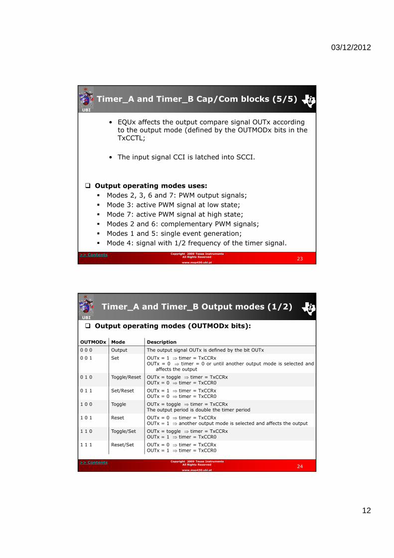
• EQUx affects the output compare signal OUTx according to the output mode (defined by the OUTMODx bits in the TxCCTL;
• The input signal CCI is latched into SCCI.
� Output operating modes uses:
� Modes 2, 3, 6 and 7: PWM output signals;
� Mode 3: active PWM signal at low state;
� Mode 7: active PWM signal at high state;
� Modes 2 and 6: complementary PWM signals;
� Modes 1 and 5: single event generation;
� Mode 4: signal with 1/2 frequency of the timer signal.
UBI
>> Contents24
Copyright 2009 Texas Instruments All Rights Reserved
www.msp430.ubi.pt
Timer_A and Timer_B Output modes (1/2)
� Output operating modes (OUTMODx bits):
OUTMODx Mode Description
0 0 0 Output The output signal OUTx is defined by the bit OUTx
0 0 1 Set OUTx = 1 ⇒ timer = TxCCRxOUTx = 0 ⇒ timer = 0 or until another output mode is selected and
affects the output
0 1 0 Toggle/Reset OUTx = toggle ⇒ timer = TxCCRxOUTx = 0 ⇒ timer = TxCCR0
0 1 1 Set/Reset OUTx = 1 ⇒ timer = TxCCRxOUTx = 0 ⇒ timer = TxCCR0
1 0 0 Toggle OUTx = toggle ⇒ timer = TxCCRxThe output period is double the timer period
1 0 1 Reset OUTx = 0 ⇒ timer = TxCCRxOUTx = 1 ⇒ another output mode is selected and affects the output
1 1 0 Toggle/Set OUTx = toggle ⇒ timer = TxCCRxOUTx = 1 ⇒ timer = TxCCR0
1 1 1 Reset/Set OUTx = 0 ⇒ timer = TxCCRxOUTx = 1 ⇒ timer = TxCCR0
03/12/2012
13
UBI
>> Contents25
Copyright 2009 Texas Instruments All Rights Reserved
www.msp430.ubi.pt
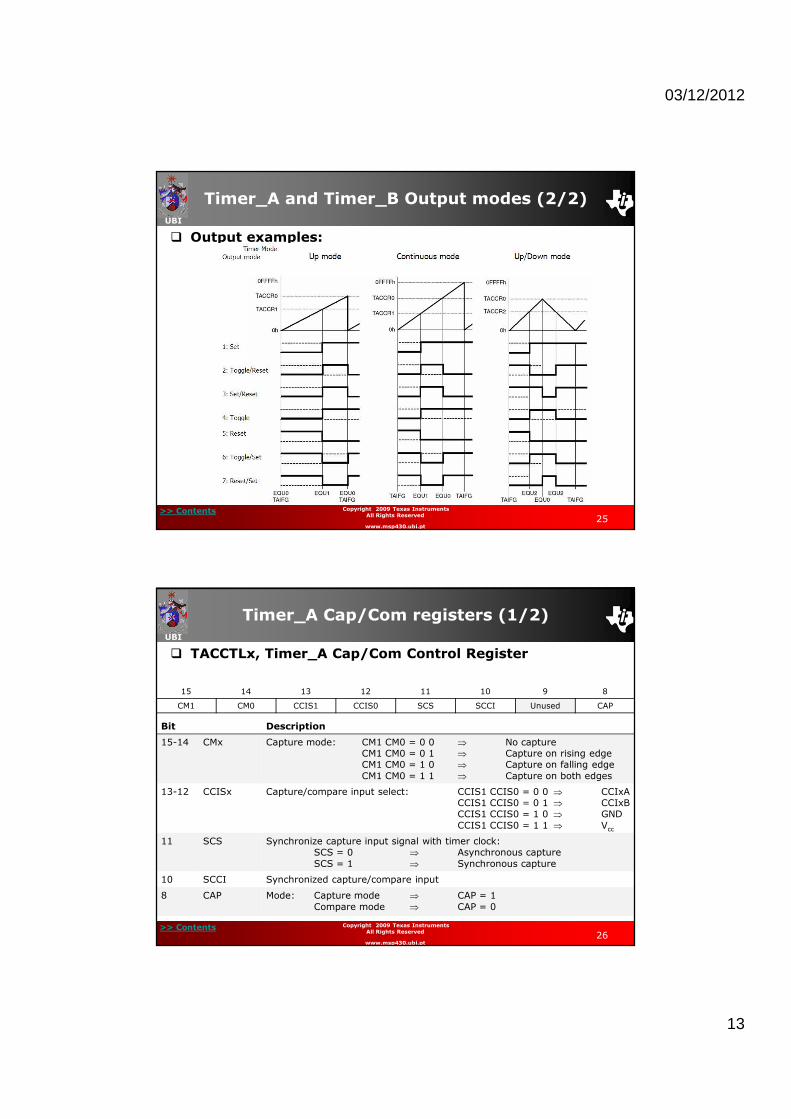
Timer_A and Timer_B Output modes (2/2)
� Output examples:
UBI
>> Contents26
Copyright 2009 Texas Instruments All Rights Reserved
www.msp430.ubi.pt
Timer_A Cap/Com registers (1/2)
� TACCTLx, Timer_A Cap/Com Control Register
15 14 13 12 11 10 9 8
CM1 CM0 CCIS1 CCIS0 SCS SCCI Unused CAP
Bit Description
15-14 CMx Capture mode: CM1 CM0 = 0 0 ⇒ No captureCM1 CM0 = 0 1 ⇒ Capture on rising edgeCM1 CM0 = 1 0 ⇒ Capture on falling edgeCM1 CM0 = 1 1 ⇒ Capture on both edges
13-12 CCISx Capture/compare input select: CCIS1 CCIS0 = 0 0 ⇒ CCIxACCIS1 CCIS0 = 0 1 ⇒ CCIxBCCIS1 CCIS0 = 1 0 ⇒ GNDCCIS1 CCIS0 = 1 1 ⇒ Vcc
11 SCS Synchronize capture input signal with timer clock:SCS = 0 ⇒ Asynchronous captureSCS = 1 ⇒ Synchronous capture
10 SCCI Synchronized capture/compare input
8 CAP Mode: Capture mode ⇒ CAP = 1Compare mode ⇒ CAP = 0

03/12/2012
14
UBI
>> Contents27
Copyright 2009 Texas Instruments All Rights Reserved
www.msp430.ubi.pt
Timer_A Cap/Com registers (2/2)
� TACCTLx, Timer_A Cap/Com Control Register
7 6 5 4 3 2 1 0
OUTMOD2 OUTMOD1 OUTMOD0 CCIE CCI OUT COV CCIFG
Bit Description
7-5 OUTMODx Output mode: OUTMOD2 OUTMOD1 OUTMOD0 = 0 0 0 ⇒ bit OUTOUTMOD2 OUTMOD1 OUTMOD0 = 0 0 1⇒ SetOUTMOD2 OUTMOD1 OUTMOD0 = 0 1 0⇒ Toggle/ResetOUTMOD2 OUTMOD1 OUTMOD0 = 0 1 1⇒ Set / ResetOUTMOD2 OUTMOD1 OUTMOD0 = 1 0 0⇒ ToggleOUTMOD2 OUTMOD1 OUTMOD0 = 1 0 1⇒ ResetOUTMOD2 OUTMOD1 OUTMOD0 = 1 1 0⇒ Toggle / SetOUTMOD2 OUTMOD1 OUTMOD0 = 1 1 1⇒ Reset / Set
4 CCIE Capture/compare interrupt enable when CCIE = 1.
3 CCI Capture/compare input
2 OUT Output state
1 COV Capture overflow when COV = 1
0 CCIFG Capture/compare interrupt flag CCIFG = 1 when interrupt pending
UBI
>> Contents28
Copyright 2009 Texas Instruments All Rights Reserved
www.msp430.ubi.pt
Timer_A and Timer_B Interrupts (1/3)
� Interrupt characteristics:
� Capture mode:
• Any CCIFG flag is set when a timer value is captured in the associated TxCCRx register.
� Compare mode:
• Any CCIFG flag is set if TxR counts up to the TxCCRx value.
• Software may also set or clear a CCIFG flag;
• All CCIFG flags request an interrupt when their corresponding CCIE bit and GIE bit are set.

03/12/2012
15
UBI
>> Contents29
Copyright 2009 Texas Instruments All Rights Reserved
www.msp430.ubi.pt
Timer_A and Timer_B Interrupts (2/3)
� Interrupt vectors associated with Timer_A:
� TACCR0 interrupt vector for TACCR0 CCIFG:
• TACCR0 CCIFG flag has the highest priority Timer_A interrupt;
• The TACCR0 CCIFG flag is automatically reset when the TACCR0 interrupt request is serviced.
UBI
>> Contents30
Copyright 2009 Texas Instruments All Rights Reserved
www.msp430.ubi.pt
Timer_A and Timer_B Interrupts (3/3)
� Interrupt vectors associated with Timer_A (continued):
� TAIV interrupt vector for TACCR1 CCIFG to TACCR4 CCIFG and TAIFG:
• Flags are given priority and combined to source a single interrupt vector (decreasing priority);
• TAIV determines which flag requests the interrupt;
• Disabling interrupts do not affect the value in TAIV;
• Any access (read/write) of TAIV automatically resets the highest pending interrupt flag;
• If another interrupt flag is set, another interrupt is immediately generated after servicing the initial interrupt.

03/12/2012
16
UBI
>> Contents31
Copyright 2009 Texas Instruments All Rights Reserved
www.msp430.ubi.pt
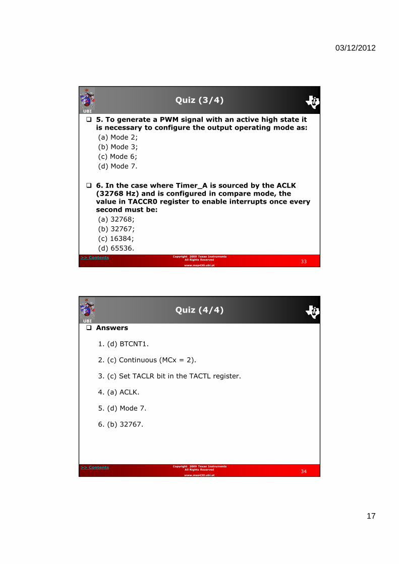
Quiz (1/4)
� 1. The timer/counter suitable for LCD controller frame frequency generation in the MSP430FG4618 is:
(a) Timer_A;
(b) BTCNT2;
(c) Timer_B;
(d) BTCNT1.
� 2. To set Timer_A to repeatedly count from 0x000 to 0xFFFF, the operating mode selected must be:
(a) Up/Down mode (MCx = 3);
(b) Up mode (MCx = 1);
(c) Continuous (MCx = 2);
(d) Stop (MCx = 0).
UBI
>> Contents32
Copyright 2009 Texas Instruments All Rights Reserved
www.msp430.ubi.pt
Quiz (2/4)
� 3. The Timer_A configured in continuous operating mode is reset with:
(a) Write 0xFFFF to TAR register;
(b) Reset TACCR0;
(c) Set TACLR bit in the TACTL register;
(d) None of the above.
� 4. When TASSELx = 1, the timer (Timer_A or Timer_B) is sourced by:
(a) ACLK;
(b) TACLK;
(c) INCLK;
(d) SMCLK.
03/12/2012
17
UBI
>> Contents33
Copyright 2009 Texas Instruments All Rights Reserved
www.msp430.ubi.pt
Quiz (3/4)
� 5. To generate a PWM signal with an active high state it is necessary to configure the output operating mode as:
(a) Mode 2;
(b) Mode 3;
(c) Mode 6;
(d) Mode 7.
� 6. In the case where Timer_A is sourced by the ACLK (32768 Hz) and is configured in compare mode, the value in TACCR0 register to enable interrupts once every second must be:
(a) 32768;
(b) 32767;
(c) 16384;
(d) 65536.
UBI
>> Contents34
Copyright 2009 Texas Instruments All Rights Reserved
www.msp430.ubi.pt
Quiz (4/4)
� Answers
1. (d) BTCNT1.
2. (c) Continuous (MCx = 2).
3. (c) Set TACLR bit in the TACTL register.
4. (a) ACLK.
5. (d) Mode 7.
6. (b) 32767.

03/12/2012
18
UBI
>> Contents
#include <msp430g2553.h>
#ifndef TIMER0_A1_VECTOR
#define TIMER0_A1_VECTOR TIMERA1_VECTOR
#define TIMER0_A0_VECTOR TIMERA0_VECTOR
#endif
volatile long tempRaw;
volatile unsigned int i;
void FaultRoutine(void);
void ConfigWDT(void);
void ConfigClocks(void);
void ConfigLEDs(void);
void ConfigADC10(void);
void ConfigTimerA2(void);
void main(void)
{
ConfigWDT();
ConfigClocks();
ConfigLEDs();
ConfigADC10();
ConfigTimerA2();
_BIS_SR(GIE);
while(1)
{
P1OUT |= BIT0;
for (i = 100; i > 0; i--);
P1OUT &= ~BIT0;
for (i = 5000; i > 0; i--);
}
}
void ConfigWDT(void)
{
WDTCTL = WDTPW + WDTHOLD; // Stop watchdog timer
}
void ConfigClocks(void)
{
if (CALBC1_1MHZ ==0xFF || CALDCO_1MHZ == 0xFF)
FaultRoutine(); // If calibration data is erased
// run FaultRoutine()
BCSCTL1 = CALBC1_1MHZ; // Set range
DCOCTL = CALDCO_1MHZ; // Set DCO step + modulation
BCSCTL3 |= LFXT1S_2; // LFXT1 = VLO
IFG1 &= ~OFIFG; // Clear OSCFault flag
BCSCTL2 |= SELM_0 + DIVM_3 + DIVS_3; // MCLK = DCO/8, SMCLK = DCO/8
}
void FaultRoutine(void)
{
P1OUT = BIT0; // P1.0 on (red LED)
while(1); // TRAP
}
void ConfigLEDs(void)
{
P1DIR = BIT6 + BIT0; // P1.6 and P1.0 outputs
P1OUT = 0; // LEDs off
}
35
Copyright 2009 Texas Instruments All Rights Reserved
www.msp430.ubi.pt
UBI
>> Contents
void ConfigADC10(void)
{
ADC10CTL1 = INCH_10 + ADC10DIV_0; // Temp Sensor ADC10CLK
}
void ConfigTimerA2(void)
{
CCTL0 = CCIE;
CCR0 = 12000;
TACTL = TASSEL_1 + MC_2;
}
#pragma vector=TIMER0_A0_VECTOR
__interrupt void Timer_A (void)
{
ADC10CTL0 = SREF_1 + ADC10SHT_3 + REFON + ADC10ON;
_delay_cycles(5); // Wait for ADC Ref to settle
ADC10CTL0 |= ENC + ADC10SC; // Sampling and conversion start
P1OUT |= BIT6; // P1.6 on (green LED)
_delay_cycles(100);
ADC10CTL0 &= ~ENC; // Disable ADC conversion
ADC10CTL0 &= ~(REFON + ADC10ON); // Ref and ADC10 off
tempRaw = ADC10MEM; // Read conversion value
P1OUT &= ~BIT6; // green LED off
CCR0 +=12000; // add 12 seconds to the timer
}
36
Copyright 2009 Texas Instruments All Rights Reserved
www.msp430.ubi.pt
03/12/2012
19
UBI
>> Contents
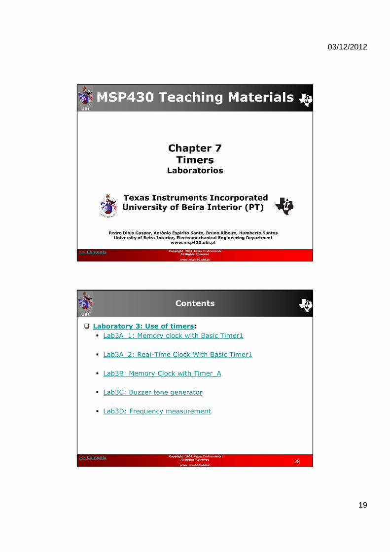
Chapter 7Timers
Laboratorios
MSP430 Teaching Materials
Texas Instruments IncorporatedUniversity of Beira Interior (PT)
Pedro Dinis Gaspar, António Espírito Santo, Bruno Ribeiro, Humberto SantosUniversity of Beira Interior, Electromechanical Engineering Department
www.msp430.ubi.pt
Copyright 2009 Texas Instruments All Rights Reserved
www.msp430.ubi.pt
UBI
>> Contents38
Copyright 2009 Texas Instruments All Rights Reserved
www.msp430.ubi.pt
Contents
� Laboratory 3: Use of timers:
� Lab3A_1: Memory clock with Basic Timer1
� Lab3A_2: Real-Time Clock With Basic Timer1
� Lab3B: Memory Clock with Timer_A
� Lab3C: Buzzer tone generator
� Lab3D: Frequency measurement

03/12/2012
20
UBI
>> Contents39
Copyright 2009 Texas Instruments All Rights Reserved
www.msp430.ubi.pt
Laboratory 3: Use of Timers
� The Labs included in this chapter cover:
• Lab3B: Memory Clock with Timer_A;
• Lab3C: Buzzer;
• Lab3D: Frequency detection.
UBI
>> Contents40
Copyright 2009 Texas Instruments All Rights Reserved
www.msp430.ubi.pt
Lab3B: Memory Clock with Timer_A
� Overview:
� The objective of the laboratory is to build a memory clock similar to the one that was developed using the Basic Timer1 in Lab3A_1;
� The Timer_A is configured to generate an interrupt once every 100 msec;
� The ISR manages of the memory clock;
� LED1 and LED2 are used to monitor the operation of the system state.

03/12/2012
21
UBI
>> Contents41
Copyright 2009 Texas Instruments All Rights Reserved
www.msp430.ubi.pt
Lab3B: Memory Clock with Timer_A
� A. Resources:
� This application makes use of Timer_A to generate an interrupt when the value in the TACCR0 unit is reached;
� The ISR updates the contents of the memory clock variables;
� LED1 is used to monitor system operation, switching state whenever Timer_A ISR runs;
� LED2 can be used to monitor the ISR execution time. The contents of the LCD is updated once every interrupt;
� When the ISR finishes, the device returns to low power mode.
UBI
>> Contents42
Copyright 2009 Texas Instruments All Rights Reserved
www.msp430.ubi.pt
Lab3B: Memory Clock with Timer_A
� A. Resources (continued):
� The system resources used by this application are:
– Timer_A;
– I/O ports;
– LCD;
– Interrupts;
– Low power modes.
� The default configuration of the FLL+ is used;
� All the clock signals required for the operation of the components of the device take their default values.

03/12/2012
22
UBI
>> Contents43
Copyright 2009 Texas Instruments All Rights Reserved
www.msp430.ubi.pt
Lab3B: Memory Clock with Timer_A
� B. Software application organization:
� The first task is to disable the Watchdog Timer;
� All the resources needed for the LCD are configured;
� This code is given;
� Once configured, the LCD is cleared by the execution of the routine LCD_all_off().
UBI
>> Contents44
Copyright 2009 Texas Instruments All Rights Reserved
www.msp430.ubi.pt
Lab3B: Memory Clock with Timer_A
� B. Software application organization (continued):
� The memory clock consists of a three global variables of type unsigned char:
• Min;
• Sec;
• Msec;
• These variables are initialized with zeros.
� The LCD is refreshed at startup to preset the clock to its initial value;
� LED2 is used as an indicator of Timer_A ISR execution;
� LED1 state switches whenever the Timer_A ISR is executed.
03/12/2012
23
UBI
>> Contents45
Copyright 2009 Texas Instruments All Rights Reserved
www.msp430.ubi.pt
Lab3B: Memory Clock with Timer_A
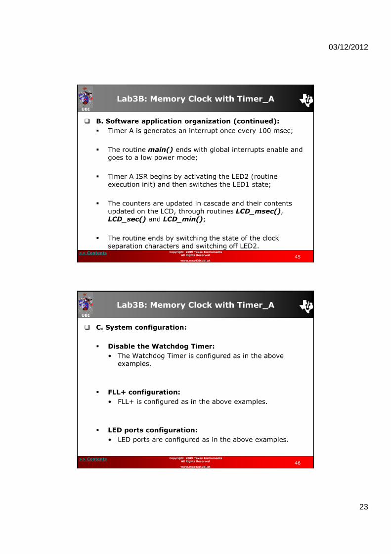
� B. Software application organization (continued):
� Timer A is generates an interrupt once every 100 msec;
� The routine main() ends with global interrupts enable and goes to a low power mode;
� Timer A ISR begins by activating the LED2 (routine execution init) and then switches the LED1 state;
� The counters are updated in cascade and their contents updated on the LCD, through routines LCD_msec(), LCD_sec() and LCD_min();
� The routine ends by switching the state of the clock separation characters and switching off LED2.
UBI
>> Contents46
Copyright 2009 Texas Instruments All Rights Reserved
www.msp430.ubi.pt
Lab3B: Memory Clock with Timer_A
� C. System configuration:
� Disable the Watchdog Timer:
• The Watchdog Timer is configured as in the above examples.
� FLL+ configuration:
• FLL+ is configured as in the above examples.
� LED ports configuration:
• LED ports are configured as in the above examples.

03/12/2012
24
UBI
>> Contents47
Copyright 2009 Texas Instruments All Rights Reserved
www.msp430.ubi.pt
Lab3B: Memory Clock with Timer_A
� C. System configuration (continued):
� Timer_A configuration:
• Timer_A is configured to count until it reaches the value contained in the TACCR0 capture/compare unit;
• An interrupt is generated when it reaches that value. Which is the interrupt vector to use? ____________
• Timer_A clock signal is the ACLK without division. What is the value to write in the configuration register?
TACTL = _____________;
UBI
>> Contents48
Copyright 2009 Texas Instruments All Rights Reserved
www.msp430.ubi.pt
Lab3B: Memory Clock with Timer_A
� C. System configuration (continued):
� Timer_A configuration:
• The TACCR0 capture/compare unit establishes the Timer_A counting range;
• For a 100 msec response, what is the value to write in the following register?
TACCR0 = ____________;
• The interrupt is configured in the TACCR0 capture/compare unit. What is the value to write to the following register:
CCTL0 = _____________;

03/12/2012
25
UBI
>> Contents49
Copyright 2009 Texas Instruments All Rights Reserved
www.msp430.ubi.pt
Lab3B: Memory Clock with Timer_A
� D. Operation analysis:
� Source code file: LAB2B_student.c;
� Solution file: LAB2B_solution.c;
� One of these files should be included in the building of the project. After the project has been compiled, debug it.
� ISR execution time:
• Using a similar approach to that described in laboratory Lab3A, measure the ISR execution time;
• What is the value determined?
• LCD refresh rate: ______
UBI
>> Contents50
Copyright 2009 Texas Instruments All Rights Reserved
www.msp430.ubi.pt
Lab3B: Memory Clock with Timer_A
� D. Operation analysis (continued):
� Measurement of electrical current drawn:
• Using a procedure similar to that described in the corresponding point of Lab3A_1, measure the value of current drawn by the device.
• What is the value measured? __________

03/12/2012
26
UBI
>> Contents51
Copyright 2009 Texas Instruments All Rights Reserved
www.msp430.ubi.pt
Lab3C: Buzzer tone generator
� Overview:
� The purpose of this laboratory is to build a sound generator using Timer B;
� The PWM signal produced by this peripheral drives the buzzer, producing a sequence of notes at regular time intervals, stored in memory;
� At the same time, LED1 and LED2 switch states alternately;
� The sound volume produced by the buzzer can be controlled through switches SW1 and SW2.
UBI
>> Contents52
Copyright 2009 Texas Instruments All Rights Reserved
www.msp430.ubi.pt
Lab3C: Buzzer tone generator
� A. Resources:
� This application requires the production of specific frequency signals corresponding to musical notes;
� For each frequency the duty-cycle can be modified in order to control the volume of sound produced;
� This task is carried out using Timer_B and one of its compare units;
� The buzzer is operated by Port P3.5 pin configured to work in its special function of TB4 output compare unit;
� This output corresponds to the TBCCR4 output compare unit.
03/12/2012
27
UBI
>> Contents53
Copyright 2009 Texas Instruments All Rights Reserved
www.msp430.ubi.pt
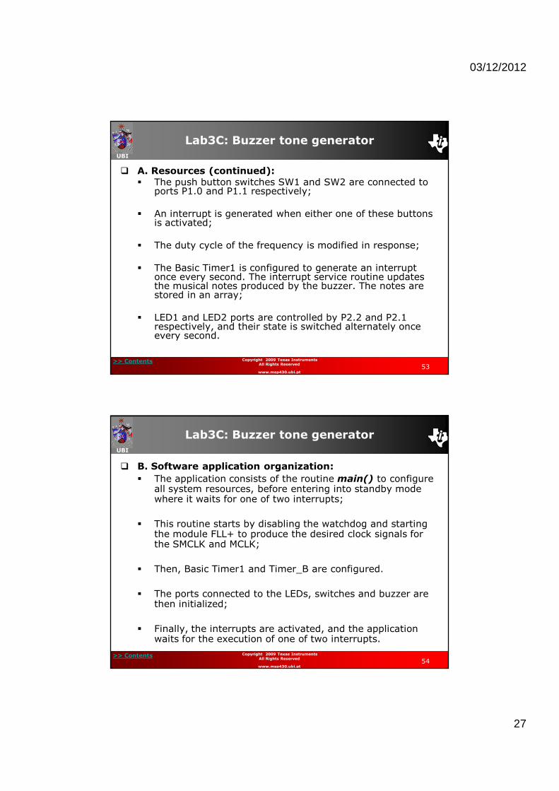
Lab3C: Buzzer tone generator
� A. Resources (continued):� The push button switches SW1 and SW2 are connected to
ports P1.0 and P1.1 respectively;
� An interrupt is generated when either one of these buttons is activated;
� The duty cycle of the frequency is modified in response;
� The Basic Timer1 is configured to generate an interrupt once every second. The interrupt service routine updates the musical notes produced by the buzzer. The notes are stored in an array;
� LED1 and LED2 ports are controlled by P2.2 and P2.1 respectively, and their state is switched alternately once every second.
UBI
>> Contents54
Copyright 2009 Texas Instruments All Rights Reserved
www.msp430.ubi.pt
Lab3C: Buzzer tone generator
� B. Software application organization:
� The application consists of the routine main() to configure all system resources, before entering into standby mode where it waits for one of two interrupts;
� This routine starts by disabling the watchdog and starting the module FLL+ to produce the desired clock signals for the SMCLK and MCLK;
� Then, Basic Timer1 and Timer_B are configured.
� The ports connected to the LEDs, switches and buzzer are then initialized;
� Finally, the interrupts are activated, and the application waits for the execution of one of two interrupts.

03/12/2012
28
UBI
>> Contents55
Copyright 2009 Texas Instruments All Rights Reserved
www.msp430.ubi.pt
Lab3C: Buzzer tone generator
� B. Software application organization (continued):� The Basic Timer1 interrupt is executed at a frequency of
once every second;
� When this interrupt is generated, it begins by switching the state of LED1 and LED2;
� Afterwards, it accesses the memory to obtain the next musical note to be processed;
� The routine ends with memory pointer management.
� The Port 1 ISR begins by evaluating the source of the interrupt ;
� The sound volume is reduced or increased by button presses of SW1 and SW2 respectively.
UBI
>> Contents56
Copyright 2009 Texas Instruments All Rights Reserved
www.msp430.ubi.pt
Lab3C: Buzzer tone generator
� C. System configuration:
� Timer_B:• It is the responsibility of Timer_B to produce the PWM signal that activates the Buzzer;
• Timer B counts until the value contained in TBCCR0 register is reached;
• It does not generate an interrupt, and must be sourced by SMCLK clock signal.
• What is the value to write to this configuration register?TBCTL = _____________;
03/12/2012
29
UBI
>> Contents57
Copyright 2009 Texas Instruments All Rights Reserved
www.msp430.ubi.pt
Lab3C: Buzzer tone generator
� C. System configuration (continued):
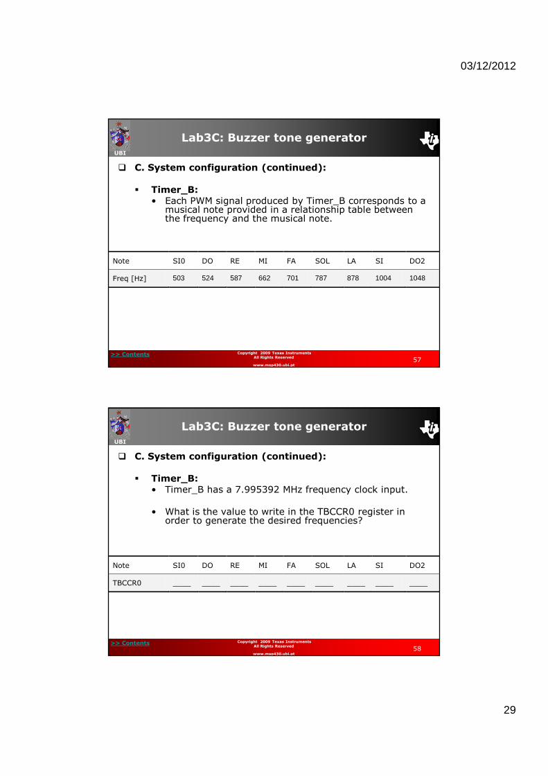
� Timer_B:• Each PWM signal produced by Timer_B corresponds to a musical note provided in a relationship table between the frequency and the musical note.
Note SI0 DO RE MI FA SOL LA SI DO2
Freq [Hz] 503 524 587 662 701 787 878 1004 1048
UBI
>> Contents58
Copyright 2009 Texas Instruments All Rights Reserved
www.msp430.ubi.pt
Lab3C: Buzzer tone generator
� C. System configuration (continued):
� Timer_B:• Timer_B has a 7.995392 MHz frequency clock input.
• What is the value to write in the TBCCR0 register in order to generate the desired frequencies?
Note SI0 DO RE MI FA SOL LA SI DO2
TBCCR0 ____ ____ ____ ____ ____ ____ ____ ____ ____

03/12/2012
30
UBI
>> Contents59
Copyright 2009 Texas Instruments All Rights Reserved
www.msp430.ubi.pt
Lab3C: Buzzer tone generator
� C. System configuration (cont):
� Timer_B:• The TBCCR4 compare unit is used to produce the PWM signal;
• The set/reset compare mode is used;
• What is the value to write in the configuration register?TBCCTL4 = _______________;
• The volume control consists of varying the PWM signal duty-cycle. Initially, its default value is 50%;
• What is the configuration to write in the register?TBCCR4 = ________________;
UBI
>> Contents60
Copyright 2009 Texas Instruments All Rights Reserved
www.msp430.ubi.pt
Lab3C: Buzzer tone generator
� C. System configuration (continued):
� Basic Timer1:• The Basic Timer1 generates an interrupt once every second;
• It uses the two counters in series, with BTCNT2 counter input selected as BTCNT1 counter output divided by 256. The BTCNT1 counter input is the ACLK clock signal with a frequency of 32768 Hz.
• If BTCNT2 counter selected output is divided by 128, what is the time period required by the Basic Timer1 interrupt? _________
• What are the values to write in configuration registers?BTCTL = __________________;IE2 = ____________________;

03/12/2012
31
UBI
>> Contents61
Copyright 2009 Texas Instruments All Rights Reserved
www.msp430.ubi.pt
Lab3C: Buzzer tone generator
� C. System configuration (continued):
� I/O Ports:• Three ports are used by this application;
• In port P1, bit P1.0 and P1.2 are used to activate the ISR whenever the buttons SW1 and SW2 are activated.
• How should just the bits related to these ports be configured in order to have digital input functions with high-to-low transition interrupts?
P1SEL &= ________________;P1DIR &= ________________;P1IFG = _________________;P1IES &= ________________;P1IE |= _________________;
UBI
>> Contents62
Copyright 2009 Texas Instruments All Rights Reserved
www.msp430.ubi.pt
Lab3C: Buzzer tone generator
� C. System configuration (continued):
� I/O Ports:• LED1 and LED2 are connected to ports P2.2 and P2.1 respectively;
• How should just the bits related to these ports be configured in order to have digital output functions?
P2DIR = ___________________;
• Configure the P2OUT register in order to initialize the application with LED1 on and LED2 off.
P2OUT = ___________________;

03/12/2012
32
UBI
>> Contents63
Copyright 2009 Texas Instruments All Rights Reserved
www.msp430.ubi.pt
Lab3C: Buzzer tone generator
� C. System configuration (continued):
� FLL+ configuration:• This module uses the 32768 Hz frequency crystal to produce a 7.995392 MHz frequency at the SMCLK and MCLK clock signals;
• What are the values to write in the following configuration registers?
FLL_CTL0 |= ________________;
SCFI0 |= ___________________;
SCFQCTL = __________________;
UBI
>> Contents64
Copyright 2009 Texas Instruments All Rights Reserved
www.msp430.ubi.pt
Lab3C: Buzzer tone generator
� D. Analysis of operation:
� System clocks inspection:
• The MCLK, SMCLK and ACLK system clocks are connected at to ports P1.1, P1.4 and P1.5 respectively;
• Using the Registers view, set bits 1, 4 and 5 of P1SEL and P1DIR registers to select the secondary function of these ports configured as outputs;
• By connecting an oscilloscope onto these lines, it is possible to monitor the clock signals;
• What are the values measured for the system clocks?ACLK: _____________________
SMCLK: ____________________
MCLK: _____________________

03/12/2012
33
UBI
>> Contents65
Copyright 2009 Texas Instruments All Rights Reserved
www.msp430.ubi.pt
Lab3C: Buzzer tone generator
� D. Analysis of operation (continued):
� TBCCR4 unit output frequency:
• With the help of the oscilloscope it is possible to evaluate the performance of the application;
• Alternatively, it is possible to listen to the sound produced;
• By removing jumper JP1 and connecting an oscilloscope probe at this point, it is possible to monitor the PWM signal produced by the microcontroller;
• The duty-cycle can be reduced or increased by activating the push button switches SW1 and SW2 respectively.
UBI
>> Contents66
Copyright 2009 Texas Instruments All Rights Reserved
www.msp430.ubi.pt
Lab3C: Buzzer tone generator
� D. Analysis of operation (continued):
� Port P1 interrupt source decoding:• All Port P1 interrupt lines share the same interrupt vector;
• Decoding is done through the P1IFG register;
• This process can be monitored by entering a breakpoint at the first line of code of the ISR;
• Execute the application;
• The execution of the application is suspended at this breakpoint when either button SW1 or SW2 is pressed;
• Press button SW1 or SW2 then run the lines of code step-by-step and observe how the registers change.
03/12/2012
34
UBI
>> Contents67
Copyright 2009 Texas Instruments All Rights Reserved
www.msp430.ubi.pt
Lab3C: Buzzer tone generator
� D. Analysis of operation (continued):
� Measurement of electrical current drawn:
• Using a procedure similar to that described at the corresponding point of Lab3A_1, measure the value of current drawn by the device.
• What is the value measured? __________
UBI
>> Contents68
Copyright 2009 Texas Instruments All Rights Reserved
www.msp430.ubi.pt
Lab3D: Frequency measurement
� Overview:
� This laboratory implements an application designed to measure the frequency of a PWM signal;
� The microcontroller can be used to generate a PWM signal based on the frequencies stored in a file, if a signal generator is not available;
� The frequencies generated are read and updated with a fixed time period using the features of CCE;
� The measured value [Hz] is shown on the LCD.

03/12/2012
35
UBI
>> Contents69
Copyright 2009 Texas Instruments All Rights Reserved
www.msp430.ubi.pt
Lab3D: Frequency measurement
� A. Resources:� The module FLL+ is configured to 7.995392 MHz frequency
for the MCLK and SMCLK clock signals;
� The program generates a PWM signal, with a frequency of 200 Hz and a duty cycle of 50%.The PWM signal frequency can be read from a file using a breakpoint (Lab3d_breakpoint.bkpt);
� This function is performed by Timer B, using the compare unit to generate the PWM signal.
� The time period between two consecutive PWM signal low-to-high transitions is measured by Timer_A;
� The capture unit of Timer_A is configured to acquire the contents of Timer A counting register when a low-to-high transition of the PWM signal is detected.
UBI
>> Contents70
Copyright 2009 Texas Instruments All Rights Reserved
www.msp430.ubi.pt
Lab3D: Frequency measurement
� A. Resources (continued):
� The Basic Timer1 generates an interrupt once every second;
� The ISR updates the frequency of the PWM signal generated by Timer_B;
� A breakpoint associated with this ISR execution allows the value of the frequency to be read from a file;
� The ports of the microcontroller are configured so that the PWM signal generated by Timer_B through the TBCCR4 compare unit (Port P3.5/TB4 - Header 7 pin 6) can be connected to the Port P1.2/TA1 (Header H2 pin 3) of the Timer_A TACCR1 capture unit;
� These pins must be connected together;
03/12/2012
36
UBI
>> Contents71
Copyright 2009 Texas Instruments All Rights Reserved
www.msp430.ubi.pt
Lab3D: Frequency measurement
� A. Resources (continued):
� Ports P2.1 and P2.2 are used to monitor the state of LED2 and LED1, respectively;
� The resources used by the application are:– Timer_A;– Timer_B;– Basic Timer1;– I/O ports;– FLL+;– Interrupts.
UBI
>> Contents72
Copyright 2009 Texas Instruments All Rights Reserved
www.msp430.ubi.pt
Lab3D: Frequency measurement
� B. Software application organization:
� The software structure allows various tasks to be performed at the same time;
� The routine main() is responsible for configuring all the resources used by the application;
� Once started, the application enables all the interrupts and waits for an interrupt request;
� Two separate routines service the possible interrupts:• TimerA1_ISR(): services interrupts generated by Timer A overflow and the TACCR1 capture unit;
• basic_timer_ISR(): services the interrupt produced by the Basic Timer1 once every second.

03/12/2012
37
UBI
>> Contents73
Copyright 2009 Texas Instruments All Rights Reserved
www.msp430.ubi.pt
Lab3D: Frequency measurement
� C. System configuration:
� Basic Timer1:• The Basic Timer1 generates an interrupt once every second;
• Use the two counters in series, with BTCNT2 counter input driven from the output of BTCNT1 counter divided by 256;
• The BTCNT1 counter input is the ACLK clock (32768 Hz)
• If BTCNT2 counter selected output is divided by 128, what is the time period of the Basic Timer1 interrupt? _________
• What are the values to write in configuration registers?BTCTL = ________________;IE2 = __________________;
UBI
>> Contents74
Copyright 2009 Texas Instruments All Rights Reserved
www.msp430.ubi.pt
Lab3D: Frequency measurement
� C. System configuration (continued):
� Timer_B:• The TBCCR4 compare unit is used to generate the PWM signal;
• The set/reset compare mode is used;
• What is the value to write in the configuration register?TBCCTL4 = ______________;
• The TB4 PWM output signal has a frequency X, with a 50% duty-cycle;
• The SMCLK clock signal is used as input of Timer_B.
03/12/2012
38
UBI
>> Contents75
Copyright 2009 Texas Instruments All Rights Reserved
www.msp430.ubi.pt
Lab3D: Frequency measurement
� C. System configuration (continued):
� Timer_B:• What is the value to write to the registers?
TBCCR0 = _______________;
TBCCR4 = _______________;
• What the highest and lowest generated frequency?– Maximum frequency value: ____________
– Minimum frequency value: _____________
UBI
>> Contents76
Copyright 2009 Texas Instruments All Rights Reserved
www.msp430.ubi.pt
Lab3D: Frequency measurement
� C. System configuration (continued):
� Timer_A:• Timer_A is sourced by the SMCLK clock signal;
• It counts to the value 0xFFFF, in continuous mode;
• An interrupt is generated when the TAR counter overflows;
• What is the value to write in its configuration register?TACTL = _________________;
03/12/2012
39
UBI
>> Contents77
Copyright 2009 Texas Instruments All Rights Reserved
www.msp430.ubi.pt
Lab3D: Frequency measurement
� C. System configuration (continued):
� Timer_A:• The capture unit compares the TAR register value to the TACCR1 register and detects a low-to-high transition at the TA1 input;
• What is the value to write in the configuration register?TACCTL1 = _______________;
• Determine the maximum and minimum frequency values detected;
UBI
>> Contents78
Copyright 2009 Texas Instruments All Rights Reserved
www.msp430.ubi.pt
Lab3D: Frequency measurement
� C. System configuration (continued):
� Timer_A:• Note that these values do not take into account the execution time of the application;
• The PWM signals should be applied at frequencies far below the maximum value determined:– Maximum frequency value: ____________– Minimum frequency value: _____________
• The TACCR1 capture unit is configured to generate an interrupt when it detects a low-to-high transition;
• What is the value to write in the configuration register?TACCTL1 = _____________;
03/12/2012
40
UBI
>> Contents79
Copyright 2009 Texas Instruments All Rights Reserved
www.msp430.ubi.pt
Lab3D: Frequency measurement
� C. System configuration (continued):
� Ports P3.5/TB4 and P1.2/TA1 configuration:• These ports perform special functions;
• Port P3.5 is configured as an output selected for the special function TB4, with the values:
P3SEL = _______________;P3DIR = _______________;
• Port P1.2 is configured as an input, selected for the special function TA1, with the values:
P1SEL = _______________;P1DIR = _______________;
UBI
>> Contents80
Copyright 2009 Texas Instruments All Rights Reserved
www.msp430.ubi.pt
Lab3D: Frequency measurement
� D. Analysis of operation:
� Run the application using the frequency generator based on Timer_B:
• Without a frequency generator, the Timer_B generates a PWM signal at the TBCCR4 unit output that can be feedback to Timer_A TACCR1 capture unit input;
• These two pins must therefore be connected together;
• By default, the PWM signal frequency is 200 Hz;
• Add a breakpoint at line 223 of code, which is for Basic Timer1 ISR and modify this value.
TBCCR0 =7995392/read_data;
03/12/2012
41
UBI
>> Contents81
Copyright 2009 Texas Instruments All Rights Reserved
www.msp430.ubi.pt
Lab3D: Frequency measurement
� D. Analysis of operation (continued):
� Run the application using a frequency generator:• The operation of the application can be measured using a frequency generator;
• The generator should generate a PWM signal with voltage and frequency values compatible with the input range of the device (2.5 to 3.3 V).
� Monitor the measured frequency:• The PWM signal applied to the TA1 input can be monitored using an oscilloscope connected to pin 3 of Header 2;
• Perform this task and confirm the values present on the LCD.
UBI
>> Contents82
Copyright 2009 Texas Instruments All Rights Reserved
www.msp430.ubi.pt
Lab3D: Frequency measurement
� D. Analysis of operation (continued):
� Measurement of electrical current drawn:• Follow the procedure described in previous laboratories to measure the current.
• What is the value measured? __________