msc8156 amc base card detailed design specifications€¦ · atca advanced telecommunications...
TRANSCRIPT
© Freescale Semiconductor, Inc., 2010. All rights reserved.
Freescale SemiconductorTechnical Data
1 Overview
1.1 ScopeThis document provides a detailed design description of the AMC base card describing its architecture, interconnect, and components.
1.2 ReferencesThe following documents are referenced for this hardware specifications:
1. MSC8156 Reference Manual
2. MSC8156 Hardware Specification
3. PICMG AMC.0 R2.0 “Advanced Mezzanine Card Base Specification”
4. PICMG AMC.2 “PCIe Advanced Mezzanine Card Base Specification”
5. PICMG AMC.4 “SRIO Advanced Mezzanine Card Base Specification”
Document Number: MSC8156AMCBCDDSRev.0, 01/2010
Contents1. Overview . . . . . . . . . . . . . . . . . . . . . . . . . . . . . . . . . . . 1
1.1. Scope. . . . . . . . . . . . . . . . . . . . . . . . . . . . . . . . . . . . . .1 1.2. References. . . . . . . . . . . . . . . . . . . . . . . . . . . . . . . . . .1 1.3. Definitions, Acronyms, and Abbreviations . . . . . . . .2
2. AMC Base Card Overview . . . . . . . . . . . . . . . . . . . . . 23. Features . . . . . . . . . . . . . . . . . . . . . . . . . . . . . . . . . . . . 44. AMC Base Card Design Description . . . . . . . . . . . . . 6
4.1. SRIO Switching Environment . . . . . . . . . . . . . . . . . .6 4.2. Ethernet . . . . . . . . . . . . . . . . . . . . . . . . . . . . . . . . . .12 4.3. System FPGA . . . . . . . . . . . . . . . . . . . . . . . . . . . . . .22 4.4. SPI . . . . . . . . . . . . . . . . . . . . . . . . . . . . . . . . . . . . . .24 4.5. I2C Interface . . . . . . . . . . . . . . . . . . . . . . . . . . . . . . .25 4.6. UART Interface. . . . . . . . . . . . . . . . . . . . . . . . . . . . .27 4.7. JTAG Interfaces . . . . . . . . . . . . . . . . . . . . . . . . . . . .28 4.8. USB Interface . . . . . . . . . . . . . . . . . . . . . . . . . . . . .29 4.9. Mezzanine Board Identification Pins . . . . . . . . . . . .30 4.10. Mezzanine High-Speed Connector Interface . . . . .31 4.11. Backplane Interface . . . . . . . . . . . . . . . . . . . . . . . .42 4.12. DIP Switches. . . . . . . . . . . . . . . . . . . . . . . . . . . . . .46 4.13. LEDs . . . . . . . . . . . . . . . . . . . . . . . . . . . . . . . . . . . .47 4.14. Push Buttons . . . . . . . . . . . . . . . . . . . . . . . . . . . . . .47 4.15. Power Supply . . . . . . . . . . . . . . . . . . . . . . . . . . . . .48 4.16. MMC. . . . . . . . . . . . . . . . . . . . . . . . . . . . . . . . . . . .53 4.17. Boundary-Scan Testing. . . . . . . . . . . . . . . . . . . . . .56 4.18. Expansion Connector and Card . . . . . . . . . . . . . . .56 4.19. Mechanicals . . . . . . . . . . . . . . . . . . . . . . . . . . . . . .57
5. Revision History . . . . . . . . . . . . . . . . . . . . . . . . . . . . 60
MSC8156 AMC Base Card Detailed Design Specification

MSC8156 AMC Base Card Detailed Design Specification, Rev.0
2 Freescale Semiconductor
AMC Base Card Overview
1.3 Definitions, Acronyms, and AbbreviationsTable 1 contains definitions, acronyms, and abbreviations used in this document.
2 AMC Base Card OverviewThe primary goals of the AMC base card are as follows:
• When fitted with MSC8156, mezzanine provides a high-density MSC8156 DSP reference platform in an AMC form factor
• Enable rapid prototyping of MSC8156-based systems for customers, third parties, and Freescale
• Specific targets include BTS systems for the WIMAX and LTE applications
• Provide design material and collateral for customers and third parties
• Create a third-party handover package that can be passed on to CEMs for any required productizing
• Provide a generic base card for future mezzanine cards, including P2020 and its derivatives
Table 1. Definitions, Acronyms, and Abbreviations
AMC Advanced Mezzanine Card (AdvancedMC™)
ATCA Advanced Telecommunications Computing Architecture
BDM Background Debug Mode
BTS Base Transceiver Station
CPLD Complex Programmable Logic Device
DIP Dual In Line Package
DNP Do Not Populate
DSP Digital Signal Processor
EEPROM Electrically Erasable Programmable Read Only Memory
FPGA Field Programmable Gate Array
GETH Giga-bit Ethernet
HSC High Speed Connector
HW Hardware
I2C(bus) Inter-Integrated Circuit
LTE Long-Term Evolution
MTCA Micro Telecommunications Computing Architecture ( MicroTCA™)
RCW Reset Configuration Word
SRIO Serial RapidIO
UART Universal Asynchronous Receiver/Transmitter
UEC UCC Gigabit Ethernet Controller
WIMAX Worldwide Interoperability for Microwave Access

MSC8156 AMC Base Card Detailed Design Specification, Rev.0
Freescale Semiconductor 3
AMC Base Card Overview
The AMC base card is designed to comply with the PICMG AMC.0 R2.0 specifications with AMC.4 (SRIO), fitting into a single-width, full-height mezzanine card. It provides Ethernet and SRIO switching capability to the mezzanines as well as general board support, such as clocks and power.
The mezzanine concept is designed to be flexible and to provide system-building blocks using devices, such as MSC8156, MSC815x, MSBA1000, and P2020. This allows AMC prototyping systems to be quickly enabled.
SRIO traffic is routed from the backplane ports [4:7], [8:11], [12:15], and [17:20] through 10-port IDT switch to the three mezzanines. Each mezzanine is connected to the SRIO switch through two x4 SRIO interfaces.
To facilitate PCIe development work, a single mezzanine site has its PCIe split from SRIO and routed directly to the backplane port [4:7] through 2:1 differential broadband Pericom PI2DBS212 multiplex/de-multiplex switch.
Gigabyte Ethernet traffic is routed from the two backplane ports 0 and 1, and from the two front panels RJ45 to three mezzanines through Vitesse VSC7384 12-port RGMII switch. The transceiver ports are configured for RGMII to 1000-Base-X conversion and routed to the backplane, while the remaining two ports are routed to the RJ45 front panel.
The FPGA collects and distributes the remaining interfacing logic, including resets, GPIOs, IRQs, LEDs, and JTAGs.
A module management controller (MMC) provides board bring up and hot swap support and sequences the power up of all components. The MMC runs on the 3.3-V management power (IPMCV).
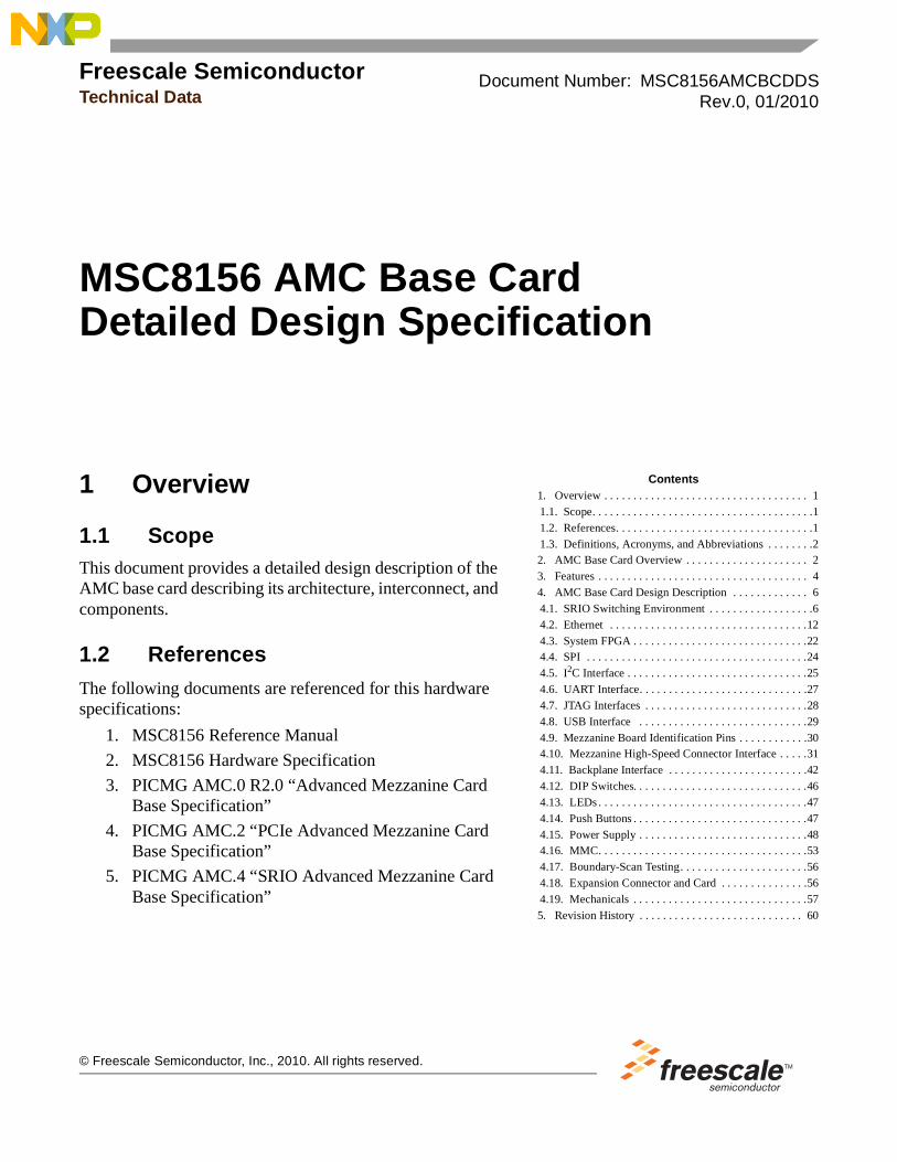
Figure 1 shows the AMC base card and MSC8156 mezzanine architecture.
NOTEThe AMC base card and MSC8156 mezzanine are jointly referred as MSC8156 AMC.
MSC8156 AMC Base Card Detailed Design Specification, Rev.0
4 Freescale Semiconductor
Features
Figure 1. AMC Base Card and MSC8156 Mezzanine Architecture (MSC8156 AMC)
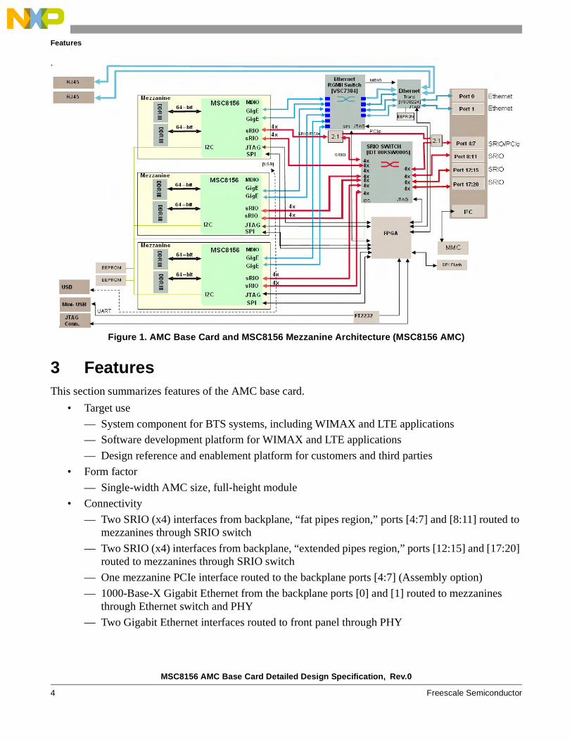
3 FeaturesThis section summarizes features of the AMC base card.
• Target use
— System component for BTS systems, including WIMAX and LTE applications
— Software development platform for WIMAX and LTE applications
— Design reference and enablement platform for customers and third parties
• Form factor
— Single-width AMC size, full-height module
• Connectivity
— Two SRIO (x4) interfaces from backplane, “fat pipes region,” ports [4:7] and [8:11] routed to mezzanines through SRIO switch
— Two SRIO (x4) interfaces from backplane, “extended pipes region,” ports [12:15] and [17:20] routed to mezzanines through SRIO switch
— One mezzanine PCIe interface routed to the backplane ports [4:7] (Assembly option)
— 1000-Base-X Gigabit Ethernet from the backplane ports [0] and [1] routed to mezzanines through Ethernet switch and PHY
— Two Gigabit Ethernet interfaces routed to front panel through PHY
MSC8156 AMC Base Card Detailed Design Specification, Rev.0
Freescale Semiconductor 5
Features
— Mezzanine UART interfaces multiplexed through the FPGA to a single mini-USB Type B connector on the front panel through a UART/USB transceiver
— Two UART ports over a single USB cable
— I2C bus connecting mezzanines for boot and configuration
— Serial peripheral interface (SPI) bus connecting mezzanines for boot and configuration
— USB v2.0 interface for P2020 development work
• Hardware blocks
— IDT CPS-10Q 10 port SRIO switch
– Two lanes of x4 SRIO from Mezzanine 1
– Two lanes of x4 SRIO from Mezzanine 2
– Two lanes of x4 SRIO from Mezzanine 3
– Two lanes of x4 SRIO to backplane ports [4:7]
– Two lanes of x4 SRIO to backplane ports [8:11]
– Two lanes of x4 SRIO to backplane ports [12:15]
– Two lanes of x4 SRIO to backplane ports [17:20]
— Ethernet switch
– Two lanes of RGMII from Mezzanine 1
– Two lanes of RGMII from Mezzanine 2
– Two lanes of RGMII from Mezzanine 3
– Two lanes of 1000-Base-X to backplane ports 0 and 1
– Two lanes of Gigabit Ethernet to front panel RJ45 connectors
• Boot
— Mezzanine boot options
– SRIO through backplane
– Ethernet through backplane or front panel
– From on-board I2C EEPROM
– From on-board serial Flash through SPI
• Debug
— All JTAGs routed through FPGA to enable full BSCAN chain during factory test
— JTAG header provided for MSC8156 mezzanines
— COP header provided for P2020 mezzanines
• Module management controller
— Hot swapping
— FRU storage
— Status LEDs
— Temperature and voltage monitoring
• Power supply

MSC8156 AMC Base Card Detailed Design Specification, Rev.0
6 Freescale Semiconductor
AMC Base Card Design Description
— 12 V payload and 3.3 V IPMCV, provided from AMC edge connector
— 12 V barrel connector for stand-alone work
— On-board voltage requirements are generated through DC–DC voltage regulators
• Connectors
— Three mezzanine high-speed connectors
— AMC edge connector
— EONCE JTAG header
— Integrated RJ45 and USB type A
— Mini-USB Type B (UART)
— Expansion connector to offload
– FPGA programming header
– MMC programming header
– COP JTAG header
– Two RS232 (MMC)
4 AMC Base Card Design DescriptionThis section provides the design details of various components of AMC base card, including hardware blocks, interfaces, and general board controls (such as switches, connectors MMC, and power).
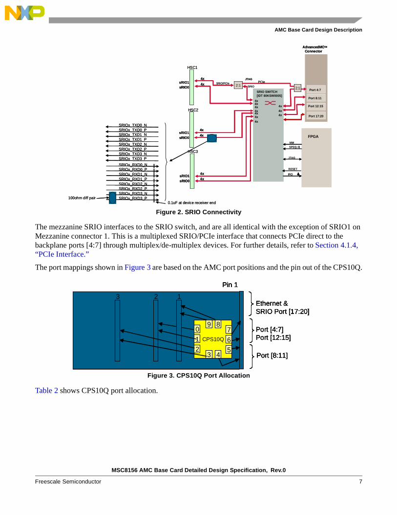
4.1 SRIO Switching EnvironmentThe IDT CPS10Q switch has high-performance SRIO interface that provides connectivity for control and data plane applications. It features ten, x4 SRIO ports running up to 3.125 GHz. Six of the ports are connected to the mezzanine connectors and four to the AMC backplane as shown in Figure 2. Out of the four, two ports interface to the fat pipes section of the AMC connector ports—[4:7] and [8:11], and the other two ports connect the extended options, backplane ports—[12:15] and [17:20].
MSC8156 AMC Base Card Detailed Design Specification, Rev.0
Freescale Semiconductor 7
AMC Base Card Design Description
Figure 2. SRIO Connectivity
The mezzanine SRIO interfaces to the SRIO switch, and are all identical with the exception of SRIO1 on Mezzanine connector 1. This is a multiplexed SRIO/PCIe interface that connects PCIe direct to the backplane ports [4:7] through multiplex/de-multiplex devices. For further details, refer to Section 4.1.4, “PCIe Interface.”
The port mappings shown in Figure 3 are based on the AMC port positions and the pin out of the CPS10Q.
Figure 3. CPS10Q Port Allocation
Table 2 shows CPS10Q port allocation.
AdvancedMCTM
Connector
Port 8:11
Port 4:7SRIO SWITCH[IDT 80KSW0005]
4x4x
4x4x
4x
4x
4x4x
4x4x 4x
4x
JTAG
2:12:1SRIO
PCIeSRIO/PCIe
sRIO0sRIO1
4x
4x
4x4x
HSC3
sRIO0sRIO1
HSC2
sRIO0sRIO1
HSC1
SRIOx_TXD0_NSRIOx_TXD0_PSRIOx_TXD1_NSRIOx_TXD1_PSRIOx_TXD2_NSRIOx_TXD2_PSRIOx_TXD3_NSRIOx_TXD3_P
SRIOx_RXD0_NSRIOx_RXD0_PSRIOx_RXD1_NSRIOx_RXD1_PSRIOx_RXD2_NSRIOx_RXD2_PSRIOx_RXD3_NSRIOx_RXD3_P100ohm diff pair
0.1uF at device receiver end
FPGAMM
IRQ
SPD[1:0]
RESET
Port 17:20
Port 12:15
JTAG
Ethernet & SRIO Port [17:20]
Port [4:7]Port [12:15]
Port [8:11]
Pin 1
CPS10Q
0
1
23 4
7
6
5
9 8
123Ethernet & SRIO Port [17:20]
Port [4:7]Port [12:15]
Port [8:11]
Pin 1
CPS10Q
0
1
23 4
7
6
5
9 8
Ethernet & SRIO Port [17:20]
Port [4:7]Port [12:15]
Port [8:11]
Pin 1
CPS10Q
0
1
23 4
7
6
5
9 8
Pin 1
CPS10Q
0
1
23 4
7
6
5
9 8
CPS10Q
0
1
23 4
7
6
5
9 8
123

MSC8156 AMC Base Card Detailed Design Specification, Rev.0
8 Freescale Semiconductor
AMC Base Card Design Description
Table 2. CPS10Q Port Allocation
Port Signal (Net name) End PointCPS10Q
Signal NameCPS10Q
IODC blocking cap
0 M2_SRIO0_TXD[0:3]_PM2_SRIO0_TXD[0:3]_N
Mezzanine 2SRIO0
RX[0:3]+RX[0:3]
I 0.1 μFat CPS10Q pins
M2_SRIO0_RXD[0:3]_PM2_SRIO0_RXD[0:3]_N
TX[0:3]+TX[0:3]-
O On mezzanine
1 M2_SRIO1_TXD[0:3]_PM2_SRIO1_TXD[0:3]_N
Mezzanine 2SRIO1
RX[4:7]+RX[4:7]-
I 0.1 μF at CPS10Q pins
M2_SRIO1_RXD[0:3]_PM2_SRIO1_RXD[0:3]_N
TX[4:7]+TX[4:7]-
O On mezzanine
2 M3_SRIO0_TXD[0:3]_PM3_SRIO0_TXD[0:3]_N
Mezzanine 3SRIO0
RX[8:11]+RX[8:11]-
I 0.1 μF at CPS10Q pins
M3_SRIO0_RXD[0:3]_PM3_SRIO0_RXD[0:3]_N
TX[8:11]+TX[8:11]-
O On mezzanine
3 M3_SRIO1_TXD[0:3]_PM3_SRIO1_TXD[0:3]_N
Mezzanine 3SRIO1
RX[12:15]+RX[12:15]-
I 0.1 μF at CPS10Q pins
M3_SRIO1_RXD[0:3]_PM3_SRIO1_RXD[0:3]_N
TX[12:15]+TX[12:15]-
O On mezzanine
4 AMC _SRIO1_TXD[0:3]_PAMC _SRIO1_TXD[0:3]_N
BackplaneSRIO1
Ports [8:11]
RX[16:19]+RX[16:19]-
I 0.1 μF at CPS10Q pins
AMC _SRIO1_RXD[0:3]_PAMC _SRIO1_RXD[0:3]_N
TX[16:19]+TX[16:19]-
O Direct connection to AMC edge connector
5 AMC_SRIO2_TXD[0:3]_PAMC_SRIO2_TXD[0:3]_N
BackplaneSRIO2
Ports[12:15]
RX[20:23]+RX[20:23]-
I 0.1 μF at CPS10Q pins
AMC _SRIO2_RXD[0:3]_PAMC _SRIO2_RXD[0:3]_N
TX[20:23]+TX[20:23]-
O Direct connection to AMC edge connector
6 AMC _SRIO0_TXD[0:3]_PAMC _SRIO0_TXD[0:3]_N
BackplaneSRIO0
Ports[4:7]
RX[16:19]+RX[16:19]-
I 0.1 μF at CPS10Q pins
AMC _SRIO0_RXD[0:3]_PAMC _SRIO0_RXD[0:3]_N
TX[16:19]+TX[16:19]-
O Connection to AMC edge connector by multiplexing
7 AMC _SRIO3_TXD[0:3]_PAMC _SRIO3_TXD[0:3]_N
BackplaneSRIO3
Ports[17:20]
RX[28:31]+RX[28:31]-
I 0.1 μF at CPS10Q pins
AMC _SRIO3_RXD[0:3]_PAMC _SRIO3_RXD[0:3]_N
TX[28:31]+TX[28:31]-
O Direct connection to AMC edge connector
8 M1_SRIO0_TXD[0:3]_PM1_SRIO0_TXD[0:3]_N
Mezzanine 1SRIO0
RX[32:35]+RX[32:35]-
I 0.1 μF at CPS10Q pins
M1_SRIO0_RXD[0:3]_PM1_SRIO0_RXD[0:3]_N
TX[32:35]+TX[32:35]-
O On mezzanine
MSC8156 AMC Base Card Detailed Design Specification, Rev.0
Freescale Semiconductor 9
AMC Base Card Design Description
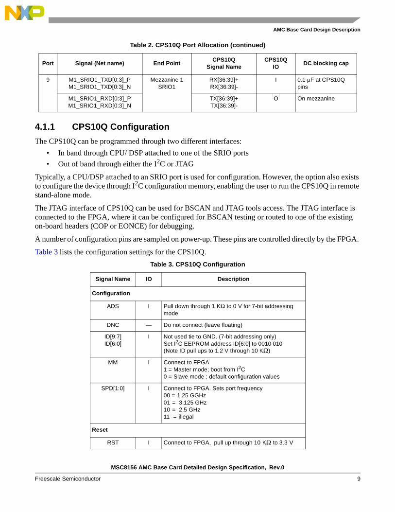
4.1.1 CPS10Q Configuration
The CPS10Q can be programmed through two different interfaces:
• In band through CPU/ DSP attached to one of the SRIO ports
• Out of band through either the I2C or JTAG
Typically, a CPU/DSP attached to an SRIO port is used for configuration. However, the option also exists to configure the device through I2C configuration memory, enabling the user to run the CPS10Q in remote stand-alone mode.
The JTAG interface of CPS10Q can be used for BSCAN and JTAG tools access. The JTAG interface is connected to the FPGA, where it can be configured for BSCAN testing or routed to one of the existing on-board headers (COP or EONCE) for debugging.
A number of configuration pins are sampled on power-up. These pins are controlled directly by the FPGA.
Table 3 lists the configuration settings for the CPS10Q.
9 M1_SRIO1_TXD[0:3]_PM1_SRIO1_TXD[0:3]_N
Mezzanine 1SRIO1
RX[36:39]+RX[36:39]-
I 0.1 μF at CPS10Q pins
M1_SRIO1_RXD[0:3]_PM1_SRIO1_RXD[0:3]_N
TX[36:39]+TX[36:39]-
O On mezzanine
Table 3. CPS10Q Configuration
Signal Name IO Description
Configuration
ADS I Pull down through 1 KΩ to 0 V for 7-bit addressing mode
DNC — Do not connect (leave floating)
ID[9:7]ID[6:0]
I Not used tie to GND. (7-bit addressing only)Set I2C EEPROM address ID[6:0] to 0010 010(Note ID pull ups to 1.2 V through 10 KΩ)
MM I Connect to FPGA 1 = Master mode; boot from I2C0 = Slave mode ; default configuration values
SPD[1:0] I Connect to FPGA. Sets port frequency00 = 1.25 GGHz01 = 3.125 GHz10 = 2.5 GHz11 = illegal
Reset
RST I Connect to FPGA, pull up through 10 KΩ to 3.3 V
Table 2. CPS10Q Port Allocation (continued)
Port Signal (Net name) End PointCPS10Q
Signal NameCPS10Q
IODC blocking cap

MSC8156 AMC Base Card Detailed Design Specification, Rev.0
10 Freescale Semiconductor
AMC Base Card Design Description
4.1.2 TerminationThe SRIO interface have a 0.1-μF DC blocking capacitor placed at the CPS10Q receiver end.
4.1.3 ClockingThe CPS10Q runs on a fixed-clock frequency of 156.25 MHz, enabling it to run at 3.125, 2.5, and 1.25 GHz. The low-jitter Vectron VCC6-L/V is used to drive the CPS10Q clocks. The LVDS to CML termination scheme uses a 2-KΩ resistor and 0.1-μF AC decoupling, as shown in Figure 4.
Figure 4. CPS10Q Clock Scheme
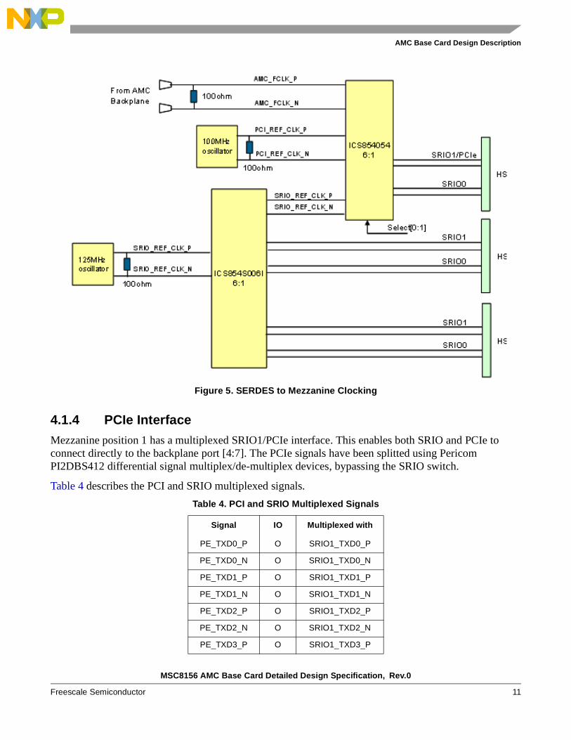
For Mezzanine 1, SRIO1 clock uses a multiplexed PCIe/SRIO clock system. For SRIO, a 125-MHz VCC6-L/V clock is switched through the ICS854054 multiplexer. For PCIe, there are two multiplexing options: a dedicated 100-MHz VCC6-L/V or an external PCIe clock from the backplane (Fabric Clock A). Two select signals control the multiplexing option and are controlled from the FPGA.
The remaining five clocks are generated from 125-MHz VCC6-L/V oscillator that are distributed to the mezzanines through ICS854S006I fan out buffer.
I2C
SCLSDA
BB
Connects to EEPROM through I2C bus (Address = 0x52)
Interrupt
IRQ O Connect to FPGA, pull up through 10 KΩ to 3.3 V
JTAG
TCKTDITDOTMSTRST
IIOII
Connect JTAG to FPGA
Table 3. CPS10Q Configuration (continued)
Signal Name IO Description
156.25MHzoscillator
SRIO_REF_CLK_P
SRIO_REF_CLK_N2K
0.1uF
0.1uF
REF_CLK_P
REF_CLK_N
CPS10Q
[LVDS-> CML Interface]
156.25MHzoscillator
SRIO_REF_CLK_P
SRIO_REF_CLK_N2K
0.1uF
0.1uF
REF_CLK_P
REF_CLK_N
CPS10Q
[LVDS-> CML Interface]
MSC8156 AMC Base Card Detailed Design Specification, Rev.0
Freescale Semiconductor 11
AMC Base Card Design Description
Figure 5. SERDES to Mezzanine Clocking
4.1.4 PCIe Interface
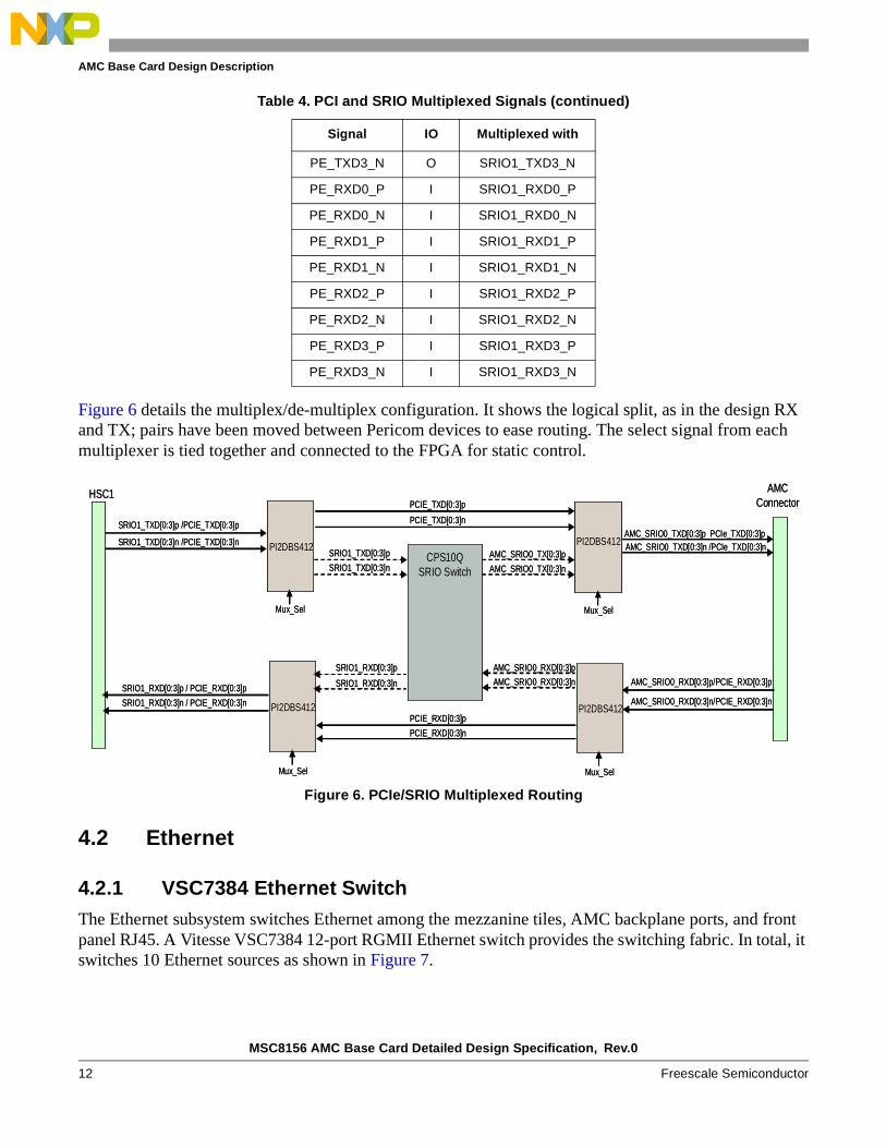
Mezzanine position 1 has a multiplexed SRIO1/PCIe interface. This enables both SRIO and PCIe to connect directly to the backplane port [4:7]. The PCIe signals have been splitted using Pericom PI2DBS412 differential signal multiplex/de-multiplex devices, bypassing the SRIO switch.
Table 4 describes the PCI and SRIO multiplexed signals.
Table 4. PCI and SRIO Multiplexed Signals
Signal IO Multiplexed with
PE_TXD0_P O SRIO1_TXD0_P
PE_TXD0_N O SRIO1_TXD0_N
PE_TXD1_P O SRIO1_TXD1_P
PE_TXD1_N O SRIO1_TXD1_N
PE_TXD2_P O SRIO1_TXD2_P
PE_TXD2_N O SRIO1_TXD2_N
PE_TXD3_P O SRIO1_TXD3_P
MSC8156 AMC Base Card Detailed Design Specification, Rev.0
12 Freescale Semiconductor
AMC Base Card Design Description
Figure 6 details the multiplex/de-multiplex configuration. It shows the logical split, as in the design RX and TX; pairs have been moved between Pericom devices to ease routing. The select signal from each multiplexer is tied together and connected to the FPGA for static control.
Figure 6. PCIe/SRIO Multiplexed Routing
4.2 Ethernet
4.2.1 VSC7384 Ethernet SwitchThe Ethernet subsystem switches Ethernet among the mezzanine tiles, AMC backplane ports, and front panel RJ45. A Vitesse VSC7384 12-port RGMII Ethernet switch provides the switching fabric. In total, it switches 10 Ethernet sources as shown in Figure 7.
PE_TXD3_N O SRIO1_TXD3_N
PE_RXD0_P I SRIO1_RXD0_P
PE_RXD0_N I SRIO1_RXD0_N
PE_RXD1_P I SRIO1_RXD1_P
PE_RXD1_N I SRIO1_RXD1_N
PE_RXD2_P I SRIO1_RXD2_P
PE_RXD2_N I SRIO1_RXD2_N
PE_RXD3_P I SRIO1_RXD3_P
PE_RXD3_N I SRIO1_RXD3_N
Table 4. PCI and SRIO Multiplexed Signals (continued)
Signal IO Multiplexed with
PI2DBS412CPS10Q
SRIO Switch
PI2DBS412
HSC1
SRIO1_TXD[0:3]p /PCIE_TXD[0:3]p
SRIO1_TXD[0:3]n /PCIE_TXD[0:3]nAMC_SRIO0_TXD[0:3]p PCIe_TXD[0:3]pAMC_SRIO0_TXD[0:3]n /PCIe_TXD[0:3]n
PI2DBS412 PI2DBS412
SRIO1_RXD[0:3]p / PCIE_RXD[0:3]p
SRIO1_RXD[0:3]n / PCIE_RXD[0:3]n
AMCConnectorPCIE_TXD[0:3]p
PCIE_TXD[0:3]n
PCIE_RXD[0:3]p
PCIE_RXD[0:3]n
AMC_SRIO0_TX[0:3]p
AMC_SRIO0_TX[0:3]n
SRIO1_TXD[0:3]p
SRIO1_TXD[0:3]n
AMC_SRIO0_RXD[0:3]p/PCIE_RXD[0:3]p
AMC_SRIO0_RXD[0:3]n/PCIE_RXD[0:3]n
AMC_SRIO0_RXD[0:3]p
AMC_SRIO0_RXD[0:3]n
SRIO1_RXD[0:3]p
SRIO1_RXD[0:3]n
Mux_Sel
Mux_Sel
Mux_Sel
Mux_Sel

MSC8156 AMC Base Card Detailed Design Specification, Rev.0
Freescale Semiconductor 13
AMC Base Card Design Description
Figure 7. Ethernet Connectivity
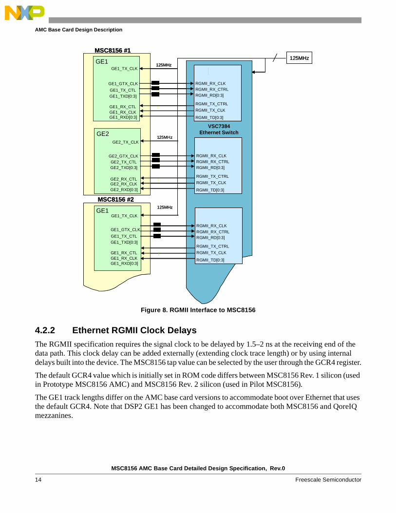
Figure 8 shows the interface between the MSC8156 and VSC7384 switch. The transmit signals from the MSC8156 mezzanine have source termination resistors, while the VS7384 transmit signals use VSC7384 device internal termination. For clocking, a 125-MHz oscillator feeds an ICS552 buffer that distributes a single clock to the Ethernet switch and two clocks to each of the mezzanines.
MSC8156 AMC Base Card Detailed Design Specification, Rev.0
14 Freescale Semiconductor
AMC Base Card Design Description
Figure 8. RGMII Interface to MSC8156
4.2.2 Ethernet RGMII Clock DelaysThe RGMII specification requires the signal clock to be delayed by 1.5–2 ns at the receiving end of the data path. This clock delay can be added externally (extending clock trace length) or by using internal delays built into the device. The MSC8156 tap value can be selected by the user through the GCR4 register.
The default GCR4 value which is initially set in ROM code differs between MSC8156 Rev. 1 silicon (used in Prototype MSC8156 AMC) and MSC8156 Rev. 2 silicon (used in Pilot MSC8156).
The GE1 track lengths differ on the AMC base card versions to accommodate boot over Ethernet that uses the default GCR4. Note that DSP2 GE1 has been changed to accommodate both MSC8156 and QoreIQ mezzanines.
VSC7384Ethernet Switch
GE1_TXD[0:3]
GE1_RX_CTL
GE1_RXD[0:3]
RGMII_RX_CTRLRGMII_RD[0:3]
GE1
RGMII_TD[0:3]
RGMII_TX_CTRL
RGMII_TX_CLKGE1_RX_CLK
GE1_TX_CLK
RGMII_RX_CLK
GE1_TX_CTL
GE1_GTX_CLK
125MHz
GE2_TXD[0:3]
GE2_RX_CTL
GE2_RXD[0:3]
RGMII_RX_CTRLRGMII_RD[0:3]
GE2
RGMII_TD[0:3]
RGMII_TX_CTRL
RGMII_TX_CLKGE2_RX_CLK
GE2_TX_CLK
RGMII_RX_CLK
GE2_TX_CTLGE2_GTX_CLK
125MHz
GE1_TXD[0:3]
GE1_RX_CTL
GE1_RXD[0:3]
RGMII_RX_CTRLRGMII_RD[0:3]
GE1
RGMII_TD[0:3]
RGMII_TX_CTRL
RGMII_TX_CLKGE1_RX_CLK
GE1_TX_CLK
RGMII_RX_CLK
GE1_TX_CTL
GE1_GTX_CLK
125MHz
125MHz
MSC8156 #2
MSC8156 #1
MSC8156 AMC Base Card Detailed Design Specification, Rev.0
Freescale Semiconductor 15
AMC Base Card Design Description
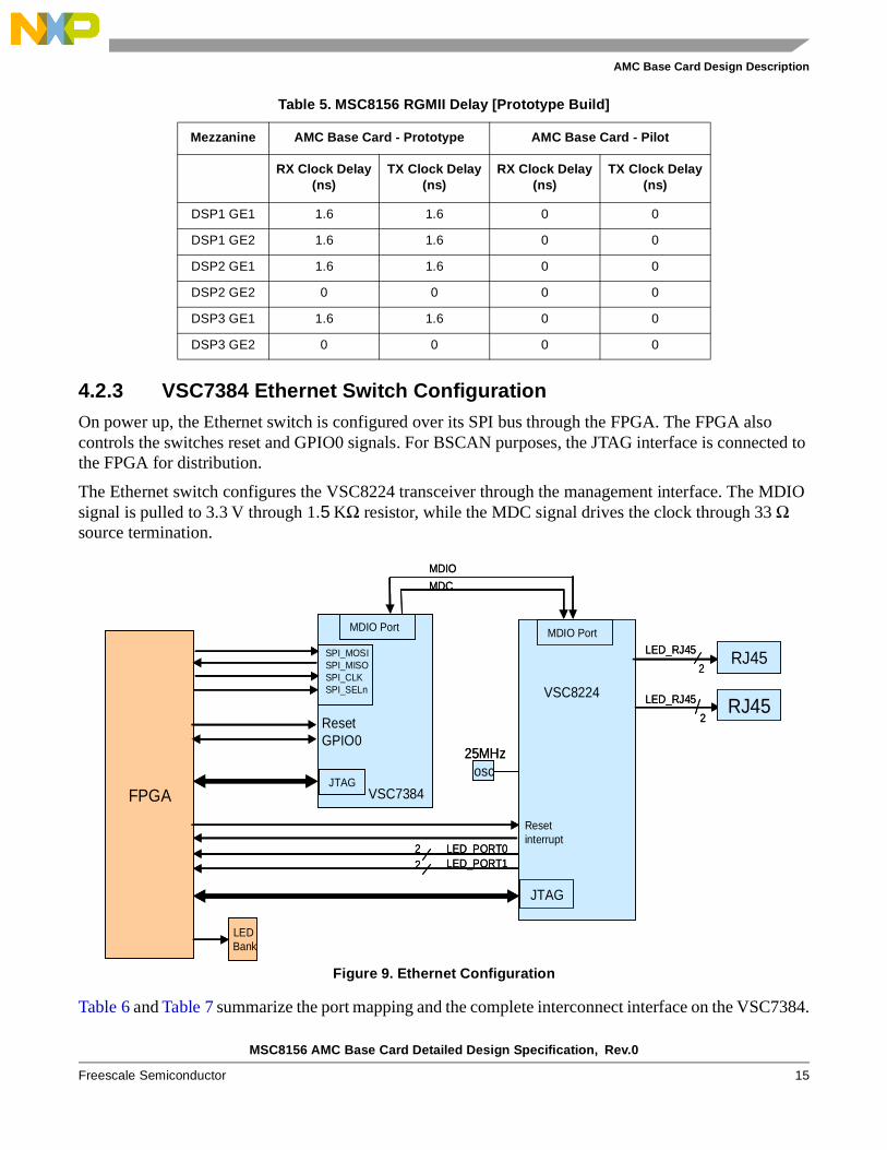
4.2.3 VSC7384 Ethernet Switch ConfigurationOn power up, the Ethernet switch is configured over its SPI bus through the FPGA. The FPGA also controls the switches reset and GPIO0 signals. For BSCAN purposes, the JTAG interface is connected to the FPGA for distribution.
The Ethernet switch configures the VSC8224 transceiver through the management interface. The MDIO signal is pulled to 3.3 V through 1.5 KΩ resistor, while the MDC signal drives the clock through 33 Ω source termination.
Figure 9. Ethernet Configuration
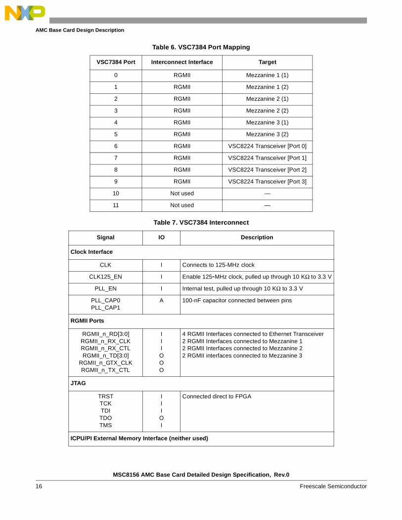
Table 6 and Table 7 summarize the port mapping and the complete interconnect interface on the VSC7384.
Table 5. MSC8156 RGMII Delay [Prototype Build]
Mezzanine AMC Base Card - Prototype AMC Base Card - Pilot
RX Clock Delay (ns)
TX Clock Delay(ns)
RX Clock Delay (ns)
TX Clock Delay (ns)
DSP1 GE1 1.6 1.6 0 0
DSP1 GE2 1.6 1.6 0 0
DSP2 GE1 1.6 1.6 0 0
DSP2 GE2 0 0 0 0
DSP3 GE1 1.6 1.6 0 0
DSP3 GE2 0 0 0 0
FPGA
SPI_MOSISPI_MISOSPI_CLKSPI_SELn
VSC7384
VSC8224
MDIO Port MDIO Port
JTAG
JTAG
LED_RJ45
LED_RJ45
osc25MHz
RJ45
RJ45
LED_PORT0
MDC
MDIO
2LED_PORT12
LEDBank
2
2ResetGPIO0
Resetinterrupt
FPGA
SPI_MOSISPI_MISOSPI_CLKSPI_SELn
VSC7384
VSC8224
MDIO Port MDIO Port
JTAG
JTAG
LED_RJ45
LED_RJ45
osc25MHz
RJ45
RJ45
LED_PORT0
MDC
MDIO
2LED_PORT12
LEDBank
2
2ResetGPIO0
Resetinterrupt
MSC8156 AMC Base Card Detailed Design Specification, Rev.0
16 Freescale Semiconductor
AMC Base Card Design Description
Table 6. VSC7384 Port Mapping
VSC7384 Port Interconnect Interface Target
0 RGMII Mezzanine 1 (1)
1 RGMII Mezzanine 1 (2)
2 RGMII Mezzanine 2 (1)
3 RGMII Mezzanine 2 (2)
4 RGMII Mezzanine 3 (1)
5 RGMII Mezzanine 3 (2)
6 RGMII VSC8224 Transceiver [Port 0]
7 RGMII VSC8224 Transceiver [Port 1]
8 RGMII VSC8224 Transceiver [Port 2]
9 RGMII VSC8224 Transceiver [Port 3]
10 Not used —
11 Not used —
Table 7. VSC7384 Interconnect
Signal IO Description
Clock Interface
CLK I Connects to 125-MHz clock
CLK125_EN I Enable 125-MHz clock, pulled up through 10 KΩ to 3.3 V
PLL_EN I Internal test, pulled up through 10 KΩ to 3.3 V
PLL_CAP0PLL_CAP1
A 100-nF capacitor connected between pins
RGMII Ports
RGMII_n_RD[3:0]RGMII_n_RX_CLKRGMII_n_RX_CTLRGMII_n_TD[3:0]
RGMII_n_GTX_CLKRGMII_n_TX_CTL
IIIOOO
4 RGMII Interfaces connected to Ethernet Transceiver2 RGMII Interfaces connected to Mezzanine 12 RGMII Interfaces connected to Mezzanine 22 RGMII interfaces connected to Mezzanine 3
JTAG
TRSTTCKTDITDOTMS
IIIOI
Connected direct to FPGA
ICPU/PI External Memory Interface (neither used)
MSC8156 AMC Base Card Detailed Design Specification, Rev.0
Freescale Semiconductor 17
AMC Base Card Design Description
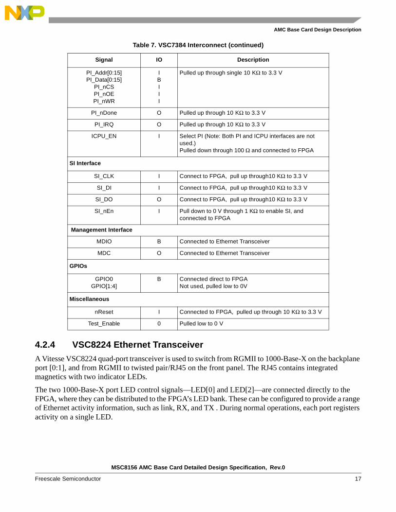
4.2.4 VSC8224 Ethernet Transceiver
A Vitesse VSC8224 quad-port transceiver is used to switch from RGMII to 1000-Base-X on the backplane port [0:1], and from RGMII to twisted pair/RJ45 on the front panel. The RJ45 contains integrated magnetics with two indicator LEDs.
The two 1000-Base-X port LED control signals—LED[0] and LED[2]—are connected directly to the FPGA, where they can be distributed to the FPGA’s LED bank. These can be configured to provide a range of Ethernet activity information, such as link, RX, and TX . During normal operations, each port registers activity on a single LED.
PI_Addr[0:15]PI_Data[0:15]
PI_nCSPI_nOEPI_nWR
IBIII
Pulled up through single 10 KΩ to 3.3 V
PI_nDone O Pulled up through 10 KΩ to 3.3 V
PI_IRQ O Pulled up through 10 KΩ to 3.3 V
ICPU_EN I Select PI (Note: Both PI and ICPU interfaces are not used.)Pulled down through 100 Ω and connected to FPGA
SI Interface
SI_CLK I Connect to FPGA, pull up through10 KΩ to 3.3 V
SI_DI I Connect to FPGA, pull up through10 KΩ to 3.3 V
SI_DO O Connect to FPGA, pull up through10 KΩ to 3.3 V
SI_nEn I Pull down to 0 V through 1 KΩ to enable SI, and connected to FPGA
Management Interface
MDIO B Connected to Ethernet Transceiver
MDC O Connected to Ethernet Transceiver
GPIOs
GPIO0GPIO[1:4]
B Connected direct to FPGANot used, pulled low to 0V
Miscellaneous
nReset I Connected to FPGA, pulled up through 10 KΩ to 3.3 V
Test_Enable 0 Pulled low to 0 V
Table 7. VSC7384 Interconnect (continued)
Signal IO Description
MSC8156 AMC Base Card Detailed Design Specification, Rev.0
18 Freescale Semiconductor
AMC Base Card Design Description
4.2.5 VSC8224 Ethernet Transceiver ConfigurationOn power up, the VSC8224 is configured through the CMODE pins. This configures a subset of the MII registers within the device. The register block can also be programmed through the management interface that connects to the Ethernet switch.
Reset control is from the FPGA that also collects the JTAG interface for BSCAN purposes. The configuration of the device is described in Table 8.
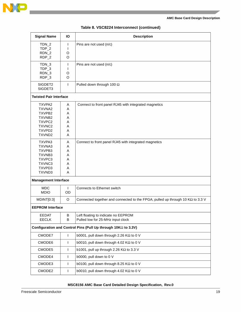
Table 8. VSC8224 Interconnect
Signal Name IO Description
RGMII Interface
TXD[3:0]_0TXCTL_0
TX_CLK_0RXD[3:0]_0RX_CLK_0RX_CTL_0
IIIOOO
Connected to Ethernet switch. The output signals have an internal 50 series termination
TXD[3:0]_1TXCTL_1
TX_CLK_1RXD[3:0]_1RX_CLK_1RX_CTL_1
IIIOOO
Connected to Ethernet switch. The output signals have an internal 50 series termination
TXD[3:0]_2TXCTL_2
TX_CLK_2RXD[3:0]_2RX_CLK_2RX_CTL_2
IIIOOO
Connected to Ethernet switch. The output signals have an internal 50 series termination
TXD[3:0]_3TXCTL_3
TX_CLK_3RXD[3:0]_3RX_CLK_3RX_CTL_3
IIIOOO
Connected to Ethernet switch. The output signals have an internal 50 series termination
SerDes Interface
TDN_0TDP_0RDN_0RDP_0
IIOO
Connected to backplane Port 0
TDN_1TDP_1RDN_1RDP_1
IIOO
Connected to backplane Port 1
SIGDET0SIGDET1
I Pulled up through 10 KΩ
MSC8156 AMC Base Card Detailed Design Specification, Rev.0
Freescale Semiconductor 19
AMC Base Card Design Description
TDN_2TDP_2RDN_2RDP_2
IIOO
Pins are not used (n/c)
TDN_3TDP_3RDN_3RDP_3
IIOO
Pins are not used (n/c)
SIGDET2SIGDET3
I Pulled down through 100 Ω
Twisted Pair Interface
TXVPA2TXVNA2TXVPB2TXVNB2TXVPC2TXVNC2TXVPD2TXVND2
AAAAAAAA
Connect to front panel RJ45 with integrated magnetics
TXVPA3TXVNA3TXVPB3TXVNB3TXVPC3TXVNC3TXVPD3TXVND3
AAAAAAAA
Connect to front panel RJ45 with integrated magnetics
Management Interface
MDCMDIO
IOD
Connects to Ethernet switch
MDINT[0:3] O Connected together and connected to the FPGA; pulled up through 10 KΩ to 3.3 V
EEPROM Interface
EEDATEECLK
BB
Left floating to indicate no EEPROMPulled low for 25-MHz input clock
Configuration and Control Pins (Pull Up through 10KΩ to 3.3V)
CMODE7 I b0001, pull down through 2.26 KΩ to 0 V
CMODE6 I b0010, pull down through 4.02 KΩ to 0 V
CMODE5 I b1001, pull up through 2.26 KΩ to 3.3 V
CMODE4 I b0000, pull down to 0 V
CMODE3 I b0100, pull down through 8.25 KΩ to 0 V
CMODE2 I b0010, pull down through 4.02 KΩ to 0 V
Table 8. VSC8224 Interconnect (continued)
Signal Name IO Description
MSC8156 AMC Base Card Detailed Design Specification, Rev.0
20 Freescale Semiconductor
AMC Base Card Design Description
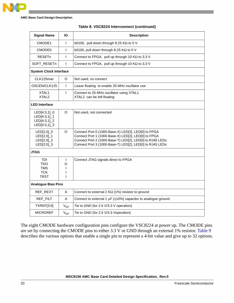
The eight CMODE hardware configuration pins configure the VSC8224 at power up. The CMODE pins are set by connecting the CMODE pins to either 3.3 V or GND through an external 1% resistor. Table 9 describes the various options that enable a single pin to represent a 4-bit value and give up to 32 options.
CMODE1 I b0100, pull down through 8.25 KΩ to 0 V
CMODE0 I b0100, pull down through 8.25 KΩ to 0 V
RESETn I Connect to FPGA, pull up through 10 KΩ to 3.3 V
SOFT_RESETn I Connect to FPGA, pull up through 10 KΩ to 3.3 V
System Clock Interface
CLK125mac O Not used, no connect
OSCEN/CLK125 I Leave floating to enable 25-MHz oscillator use
XTAL1XTAL2
I Connect to 25-MHz oscillator using XTAL1XTAL2 can be left floating
LED Interface
LED[4:3,1]_0LED[4:3,1]_1LED[4:3,1]_2LED[4:3,1]_3
O Not used, not connected
LED[2,0]_0LED[2,0]_1LED[2,0[_2LED[2:0]_3
O Connect Port 0 (1000-Base-X) LED[2], LED[0] to FPGAConnect Port 1 (1000-Base-X) LED[2], LED[0] to FPGAConnect Port 2 (1000-Base-T) LED[2], LED[0] to RJ45 LEDsConnect Port 3 (1000-Base-T) LED[2], LED[0] to RJ45 LEDs
JTAG
TDITDOTMSTCK
TRST
IOIII
Connect JTAG signals direct to FPGA
Analogue Bias Pins
REF_REXT A Connect to external 2 KΩ (1%) resistor to ground
REF_FILT A Connect to external 1 μF (±10%) capacitor to analogue ground
TXREF[3:0] Vref Tie to GND (for 2.5 V/3.3 V operation)
MICROREF Vref Tie to GND (for 2.5 V/3.3 Voperation)
Table 8. VSC8224 Interconnect (continued)
Signal Name IO Description

MSC8156 AMC Base Card Detailed Design Specification, Rev.0
Freescale Semiconductor 21
AMC Base Card Design Description
The hardware configuration variables that can be changed are described in Table 10, while the actual settings used are described in Table 11.
Table 9. CMODE Pin Combinations
CMODE3:0 CMODE Resistor Value Tied to 0 V or 3.3 V
0000 0 Ω 0 V
0001 2.26 kΩ 0 V
0010 4.02 kΩ 0 V
0011 5.90 kΩ 0 V
0100 8.25 kΩ 0 V
0101 12.1 kΩ 0 V
0110 16.9kΩ 0 V
0111 22.6 kΩ 0 V
1000 0 Ω 3.3 V
1001 2.26 kΩ 3.3 V
1010 4.02 kΩ 3.3 V
1011 5.90 kΩ 3.3 V
1100 8.25 kΩ 3.3 V
1101 12.1 kΩ 3.3 V
1110 16.9 kΩ 3.3 V
1111 22.6 kΩ 3.3 V
Table 10. CMODE Hardware Configuration Bits
CMODE Pin Bit [3] Bit [2] Bit[1] Bit[0] Encoding
7 RGMII Clock Skew[1] SIGDET pin direction ActiPHY Link Speed Downshift
0001
6 RGMII Clock Skew[0] Remote Fault Control [1] LED Combine link/act
LED Pulse Stretch Blink
0010
5 PHY Address [4] Remote Fault Control [2] LED Combine Link
10/100/1000/Act
LED Combine COL/DUP
1001
4 PHY Address [3] Speed/Dup Mode [0] LED4[1] LED4[0] 0000
3 PHY Address [2] Speed/Dup Mode [1] LED3[1] LED3[0] 0100
2 MAC Interface [3] 0 LED2[1] LED2[0] 0010
1 MAC Interface [2] Pause Control [1] LED1[1] LED1[0] 0100
0 MAC Interface [1] Pause Control [2] LED0[1] LED0[0] 0100
MSC8156 AMC Base Card Detailed Design Specification, Rev.0
22 Freescale Semiconductor
AMC Base Card Design Description
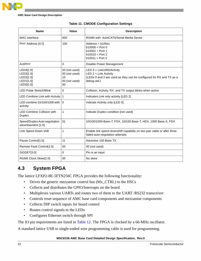
4.3 System FPGAThe lattice LFXP2-8E-5FTN256C FPGA provides the following functionality:
• Drives the generic mezzanine control bus (Mx_CTRL) to the HSCs
• Collects and distributes the GPIO/Interrupts on the board
• Multiplexes various UARTs and routes two of them to the UART /RS232 transceiver
• Controls reset sequence of AMC base card components and mezzanine components
• Collects DIP switch inputs for board control
• Routes control signals to the LEDs
• Configures Ethernet switch through SPI
The IO pin requirements are listed in Table 12. The FPGA is clocked by a 66-MHz oscillator.
A standard lattice USB to single-ended wire programming cable is used for programming.
Table 11. CMODE Configuration Settings
Name Value Description
MAC Interface 000 RGMII with AutoCAT5/Serial Media Sense
PHY Address [4:2] 100 Address = b100xxb10000 = Port 0b10001 = Port 1b10010 = Port 2b10011 = Port 3
ActiPHY 0 Disable Power Management
LED4[1:0]LED3[1:0]LED2[1:0]LED1[1:0]LED0[1:0]
00 (not used)00 (not used)1000 (not used)00
LED 0 = Link1000/ActivityLED 2 = Link Activity(LEDs 0 and 2 are used as they can be configured for RX and TX as a debug aid.)
LED Pulse Stretch/Blink 0 Collision, Activity, RX and TX output blinks when active
LED Combine Link with Activity 1 Indicates Link only activity [LED 2]
LED combine 10/100/1000 with activity
0 Indicate Activity only [LED 0]
LED Combine Collision with Duplex
1 Indicate Duplex condition [not used]
Speed/Duplex Auto negotiation advertisement [1:0]
01 10/100/1000-Base-T, FDX, 10/100 Base-T, HDX, 1000 Base-X, FDX
Link Speed Down shift 1 Enable link speed downshift capability on two-pair cable or after three failed auto-negotation attempts
Pause Control[1:0] 11 Advertise 100 Base TX
Remote Fault Control[1:0] 00 00 (not used)
SIGDET[3:0] 0 Pin is an input
RGMII Clock Skew[1:0] 00 No skew
MSC8156 AMC Base Card Detailed Design Specification, Rev.0
Freescale Semiconductor 23
AMC Base Card Design Description
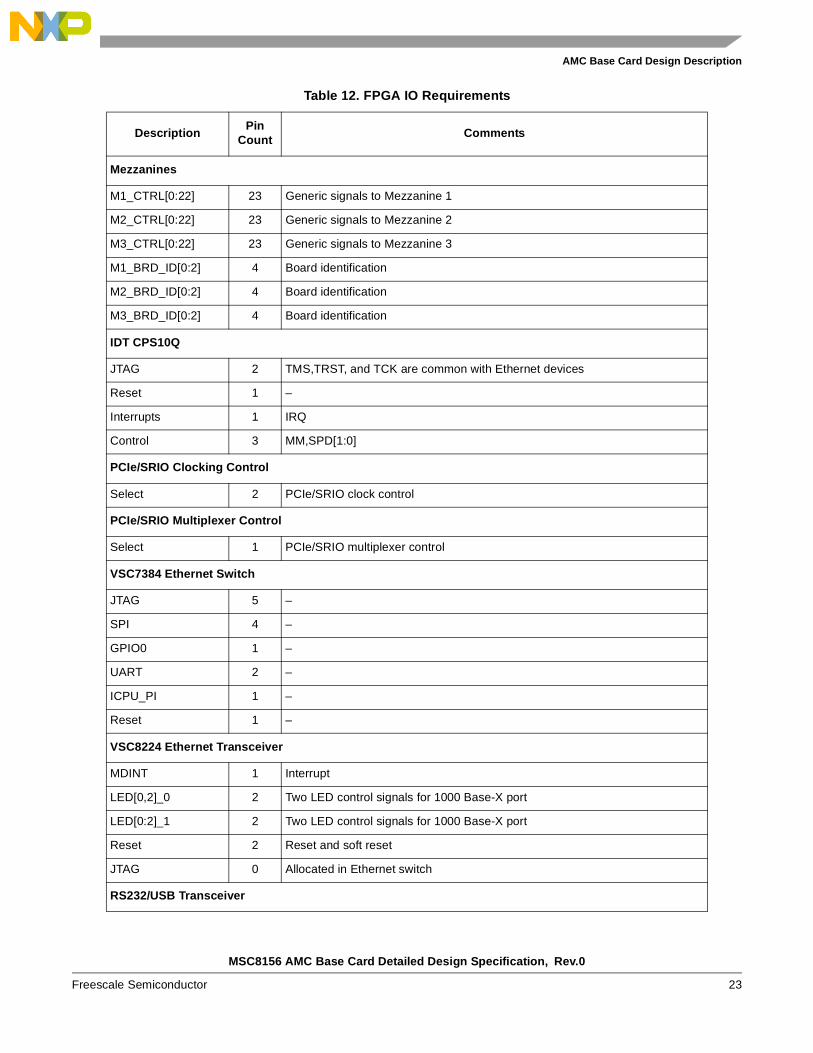
Table 12. FPGA IO Requirements
Description Pin
CountComments
Mezzanines
M1_CTRL[0:22] 23 Generic signals to Mezzanine 1
M2_CTRL[0:22] 23 Generic signals to Mezzanine 2
M3_CTRL[0:22] 23 Generic signals to Mezzanine 3
M1_BRD_ID[0:2] 4 Board identification
M2_BRD_ID[0:2] 4 Board identification
M3_BRD_ID[0:2] 4 Board identification
IDT CPS10Q
JTAG 2 TMS,TRST, and TCK are common with Ethernet devices
Reset 1 –
Interrupts 1 IRQ
Control 3 MM,SPD[1:0]
PCIe/SRIO Clocking Control
Select 2 PCIe/SRIO clock control
PCIe/SRIO Multiplexer Control
Select 1 PCIe/SRIO multiplexer control
VSC7384 Ethernet Switch
JTAG 5 –
SPI 4 –
GPIO0 1 –
UART 2 –
ICPU_PI 1 –
Reset 1 –
VSC8224 Ethernet Transceiver
MDINT 1 Interrupt
LED[0,2]_0 2 Two LED control signals for 1000 Base-X port
LED[0:2]_1 2 Two LED control signals for 1000 Base-X port
Reset 2 Reset and soft reset
JTAG 0 Allocated in Ethernet switch
RS232/USB Transceiver
MSC8156 AMC Base Card Detailed Design Specification, Rev.0
24 Freescale Semiconductor
AMC Base Card Design Description
4.3.1 FPGA programmingThe FPGA programming header is located on the expansion card; see section Section 4.18, “Expansion Connector and Card.”
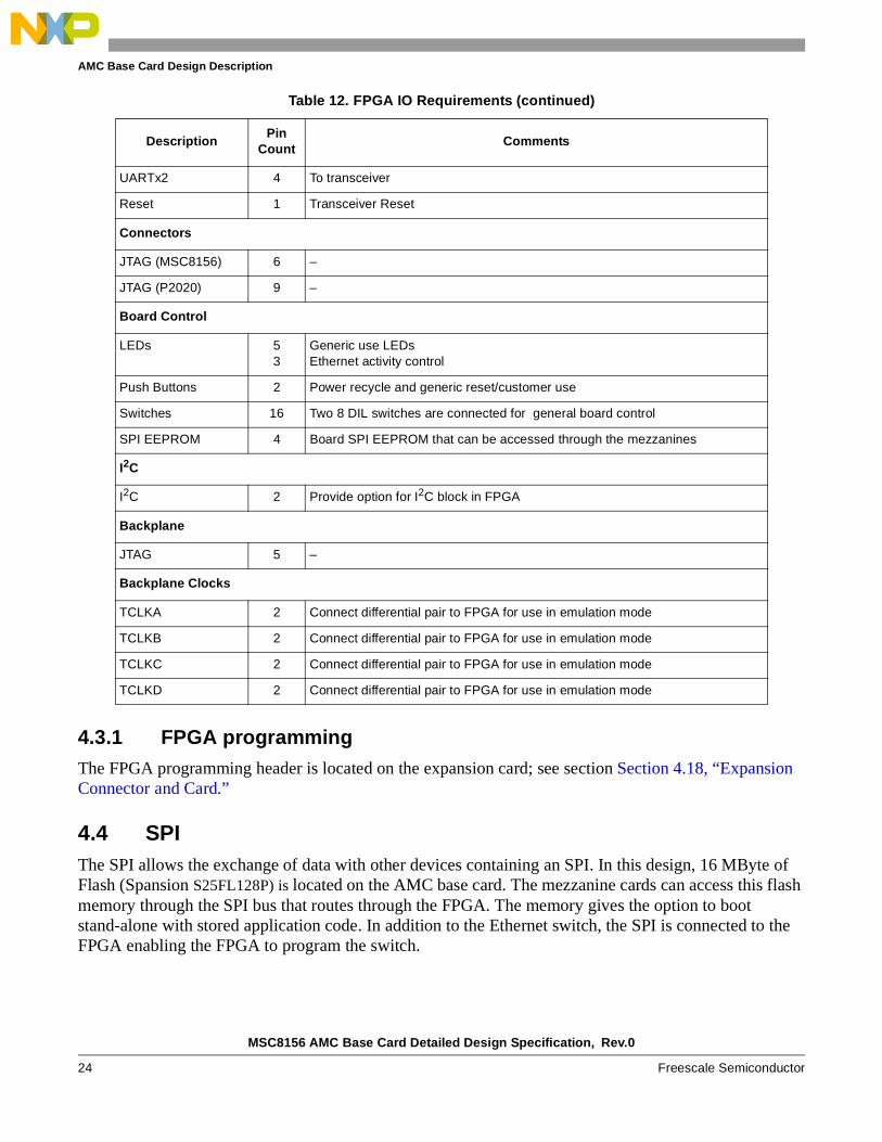
4.4 SPI The SPI allows the exchange of data with other devices containing an SPI. In this design, 16 MByte of Flash (Spansion S25FL128P) is located on the AMC base card. The mezzanine cards can access this flash memory through the SPI bus that routes through the FPGA. The memory gives the option to boot stand-alone with stored application code. In addition to the Ethernet switch, the SPI is connected to the FPGA enabling the FPGA to program the switch.
UARTx2 4 To transceiver
Reset 1 Transceiver Reset
Connectors
JTAG (MSC8156) 6 –
JTAG (P2020) 9 –
Board Control
LEDs 53
Generic use LEDsEthernet activity control
Push Buttons 2 Power recycle and generic reset/customer use
Switches 16 Two 8 DIL switches are connected for general board control
SPI EEPROM 4 Board SPI EEPROM that can be accessed through the mezzanines
I2C
I2C 2 Provide option for I2C block in FPGA
Backplane
JTAG 5 –
Backplane Clocks
TCLKA 2 Connect differential pair to FPGA for use in emulation mode
TCLKB 2 Connect differential pair to FPGA for use in emulation mode
TCLKC 2 Connect differential pair to FPGA for use in emulation mode
TCLKD 2 Connect differential pair to FPGA for use in emulation mode
Table 12. FPGA IO Requirements (continued)
Description Pin
CountComments

MSC8156 AMC Base Card Detailed Design Specification, Rev.0
Freescale Semiconductor 25
AMC Base Card Design Description
The SPI bus has been routed through the FPGA to give the user a choice of using the mezzanine SPIO pins as GPIO, if the SPI option is not used. The four SPI signals, SPI_SL, SPICLK, SPIMOS, and SPIMISO have 20 KΩ pull ups. The block diagram for SPI is shown in Figure 10 .
Figure 10. SPI
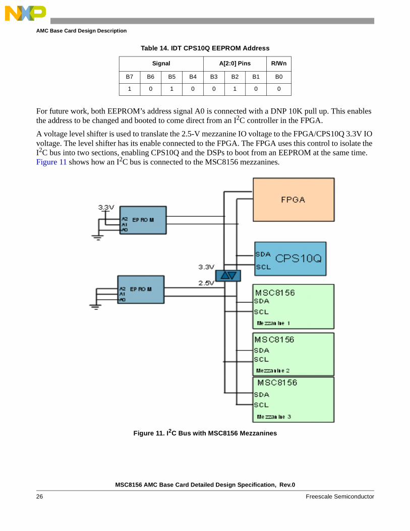
4.5 I2C InterfaceThe I2C bus connects the three mezzanines, FPGA and the CPS10Q together. Also it provides a method for bootstrap and communication, as shown in Figure 11.
Two EEPROMs are provided on the bus. One is for the MSC8156 mezzanines and the other for the CPS10Q.
The MSC8156 mezzanines access the I2C bus at address 0x50, which represents the EEPROM. Bits B[7:4] = b1010 are hard coded into the EEPROM device, while the bits B[3:1] are defined by the A[2:0] pins, which are tied low as described in Table 13. The final bit, B0, is set by the read/write signal. The Write Protect feature on the EEPROM is not required and is tied low.
The CPS10Q I2C interface boots from a dedicated I2C EEPROM (M24512-WMW6T) at address 0x52. Table 14 describes the addressing for the CPS10Q EEPROM .
Table 13. MSC8156 Mezzanine Configuration EEPROM Address
Signal A[2:0] pins R/Wn
B7 B6 B5 B4 B3 B2 B1 B0
1 0 1 0 0 0 0 0
SPI_MOSISPI_MISOSPI_CLKSPI_SELn SI
SOSCKCS
FLASH
Mezzanine 1
SI_DISI_DOSI_CLKSI_EN
Ethernet Switch
SPI_MOSISPI_MISOSPI_CLKSPI_SELn
Mezzanine 2
SPI_MOSISPI_MISOSPI_CLKSPI_SELn
Mezzanine 3
FPGA
SPI_MOSISPI_MISOSPI_CLKSPI_SELn SI
SOSCKCS
FLASH
Mezzanine 1
SI_DISI_DOSI_CLKSI_EN
Ethernet Switch
SPI_MOSISPI_MISOSPI_CLKSPI_SELn
Mezzanine 2
SPI_MOSISPI_MISOSPI_CLKSPI_SELn
Mezzanine 3
FPGA
MSC8156 AMC Base Card Detailed Design Specification, Rev.0
26 Freescale Semiconductor
AMC Base Card Design Description
For future work, both EEPROM’s address signal A0 is connected with a DNP 10K pull up. This enables the address to be changed and booted to come direct from an I2C controller in the FPGA.
A voltage level shifter is used to translate the 2.5-V mezzanine IO voltage to the FPGA/CPS10Q 3.3V IO voltage. The level shifter has its enable connected to the FPGA. The FPGA uses this control to isolate the I2C bus into two sections, enabling CPS10Q and the DSPs to boot from an EEPROM at the same time. Figure 11 shows how an I2C bus is connected to the MSC8156 mezzanines.
Figure 11. I2C Bus with MSC8156 Mezzanines
Table 14. IDT CPS10Q EEPROM Address
Signal A[2:0] Pins R/Wn
B7 B6 B5 B4 B3 B2 B1 B0
1 0 1 0 0 1 0 0
MSC8156 AMC Base Card Detailed Design Specification, Rev.0
Freescale Semiconductor 27
AMC Base Card Design Description
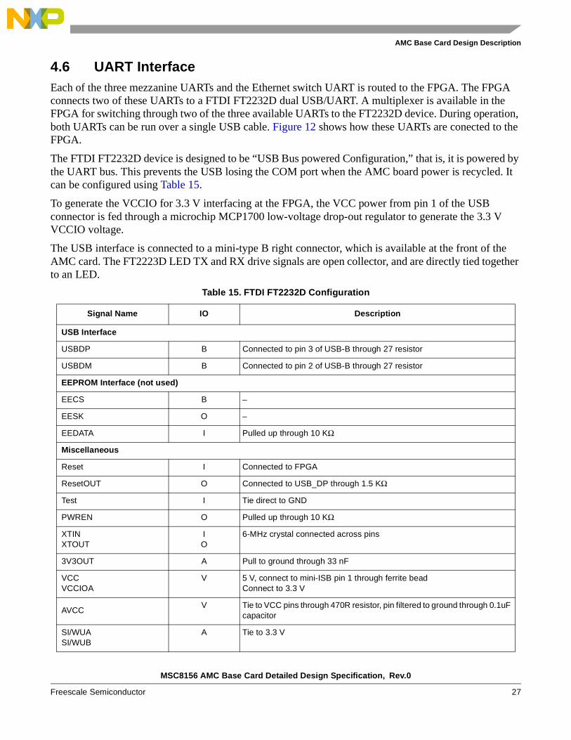
4.6 UART InterfaceEach of the three mezzanine UARTs and the Ethernet switch UART is routed to the FPGA. The FPGA connects two of these UARTs to a FTDI FT2232D dual USB/UART. A multiplexer is available in the FPGA for switching through two of the three available UARTs to the FT2232D device. During operation, both UARTs can be run over a single USB cable. Figure 12 shows how these UARTs are conected to the FPGA.
The FTDI FT2232D device is designed to be “USB Bus powered Configuration,” that is, it is powered by the UART bus. This prevents the USB losing the COM port when the AMC board power is recycled. It can be configured using Table 15.
To generate the VCCIO for 3.3 V interfacing at the FPGA, the VCC power from pin 1 of the USB connector is fed through a microchip MCP1700 low-voltage drop-out regulator to generate the 3.3 V VCCIO voltage.
The USB interface is connected to a mini-type B right connector, which is available at the front of the AMC card. The FT2223D LED TX and RX drive signals are open collector, and are directly tied together to an LED.
Table 15. FTDI FT2232D Configuration
Signal Name IO Description
USB Interface
USBDP B Connected to pin 3 of USB-B through 27 resistor
USBDM B Connected to pin 2 of USB-B through 27 resistor
EEPROM Interface (not used)
EECS B –
EESK O –
EEDATA I Pulled up through 10 KΩ
Miscellaneous
Reset I Connected to FPGA
ResetOUT O Connected to USB_DP through 1.5 KΩ
Test I Tie direct to GND
PWREN O Pulled up through 10 KΩ
XTINXTOUT
IO
6-MHz crystal connected across pins
3V3OUT A Pull to ground through 33 nF
VCCVCCIOA
V 5 V, connect to mini-ISB pin 1 through ferrite beadConnect to 3.3 V
AVCCV Tie to VCC pins through 470R resistor, pin filtered to ground through 0.1uF
capacitor
SI/WUASI/WUB
A Tie to 3.3 V

MSC8156 AMC Base Card Detailed Design Specification, Rev.0
28 Freescale Semiconductor
AMC Base Card Design Description
Figure 12. UART Interfacing
4.7 JTAG InterfacesThe MSC8156 EONCE module allows nonintrusive interaction with the SC3850 core, enabling examination/analysis of registers, memory, and on-chip peripherals. The EONCE module connects with the debugging system through the on-chip JTAG TAP controller pins.
UART Interface Channel A
TXDA (ADBUS0) O Connect to FPGA through 1KΩ (to limit current)
RXDA (ADBUS1) I Connect to FPGA
ABBUS[2:7] IO No connect (internal pull ups)
UART Interface Channel B
TXDB (BDBUS0) O Connect to FPGA through 1 KΩ (to limit current)
RXDB (BDBUS1) I Connect to FPGA
BBBUS[2:7] IO No connect (internal pull ups)
LEDS
TXLEDRXLED
OC TXLED and RX LED (four signals) tied together and connected to orange LED
Table 15. FTDI FT2232D Configuration (continued)
Signal Name IO Description
Mezzanine #3
UART_TXD
UART_RXD
FT2232DUART_TXD1
UART_RXD1
UART_TXD0
UART_RXD0
FPGA
USBDM USBDP
MiniUSB
1234
VCCIO VCC
LDOMezzanine #2
UART_TXD
UART_RXD
Mezzanine #1
UART_TXD
UART_RXD
VSC7384
UART_TXD
UART_RXD
Switch select
Mezzanine #3
UART_TXD
UART_RXD
FT2232DUART_TXD1
UART_RXD1
UART_TXD0
UART_RXD0
FPGA
USBDM USBDP
MiniUSB
1234
VCCIO VCC
LDOMezzanine #2
UART_TXD
UART_RXD
Mezzanine #1
UART_TXD
UART_RXD
VSC7384
UART_TXD
UART_RXD
Mezzanine #3
UART_TXD
UART_RXD
Mezzanine #3
UART_TXD
UART_RXD
FT2232DUART_TXD1
UART_RXD1
UART_TXD0
UART_RXD0
FPGA
USBDM USBDP
MiniUSB
1234
VCCIO VCC
LDOMezzanine #2
UART_TXD
UART_RXD
Mezzanine #2
UART_TXD
UART_RXD
Mezzanine #1
UART_TXD
UART_RXD
Mezzanine #1
UART_TXD
UART_RXD
VSC7384
UART_TXD
UART_RXD
VSC7384
UART_TXD
UART_RXD
Switch select
MSC8156 AMC Base Card Detailed Design Specification, Rev.0
Freescale Semiconductor 29
AMC Base Card Design Description
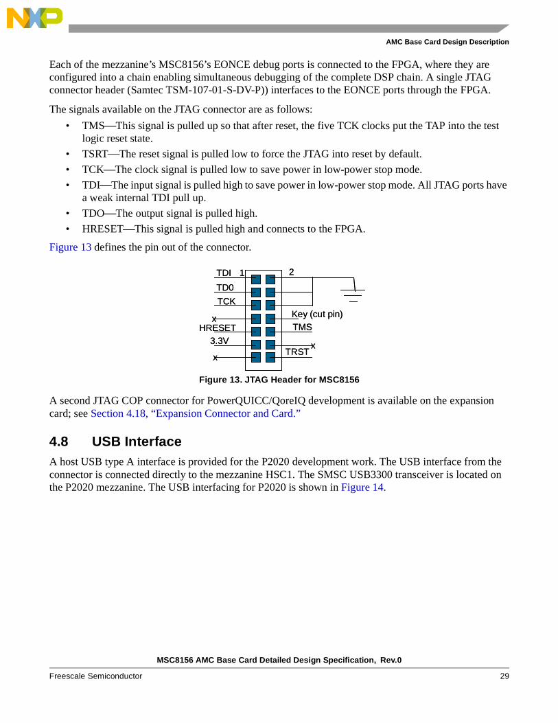
Each of the mezzanine’s MSC8156’s EONCE debug ports is connected to the FPGA, where they are configured into a chain enabling simultaneous debugging of the complete DSP chain. A single JTAG connector header (Samtec TSM-107-01-S-DV-P)) interfaces to the EONCE ports through the FPGA.
The signals available on the JTAG connector are as follows:
• TMS⎯This signal is pulled up so that after reset, the five TCK clocks put the TAP into the test logic reset state.
• TSRT⎯The reset signal is pulled low to force the JTAG into reset by default.
• TCK⎯The clock signal is pulled low to save power in low-power stop mode.
• TDI⎯The input signal is pulled high to save power in low-power stop mode. All JTAG ports have a weak internal TDI pull up.
• TDO⎯The output signal is pulled high.
• HRESET⎯This signal is pulled high and connects to the FPGA.
Figure 13 defines the pin out of the connector.
Figure 13. JTAG Header for MSC8156
A second JTAG COP connector for PowerQUICC/QoreIQ development is available on the expansion card; see Section 4.18, “Expansion Connector and Card.”
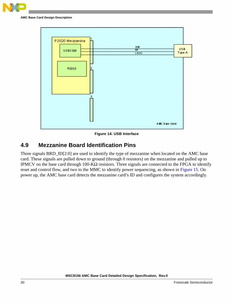
4.8 USB Interface A host USB type A interface is provided for the P2020 development work. The USB interface from the connector is connected directly to the mezzanine HSC1. The SMSC USB3300 transceiver is located on the P2020 mezzanine. The USB interfacing for P2020 is shown in Figure 14.
1 2TDI
TD0
TCK
xHRESET
3.3V
x
Key (cut pin)TMS
TRSTx
1 2TDI
TD0
TCK
xHRESET
3.3V
x
Key (cut pin)TMS
TRSTx
MSC8156 AMC Base Card Detailed Design Specification, Rev.0
30 Freescale Semiconductor
AMC Base Card Design Description
Figure 14. USB Interface
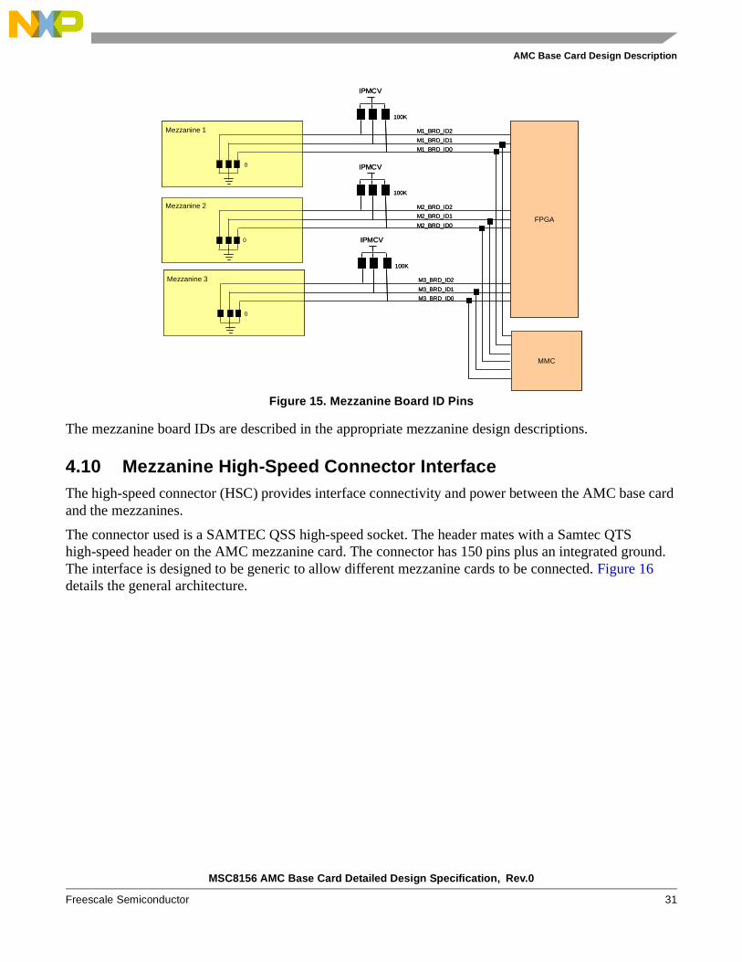
4.9 Mezzanine Board Identification PinsThree signals BRD_ID[2:0] are used to identify the type of mezzanine when located on the AMC base card. These signals are pulled down to ground (through 0 resistors) on the mezzanine and pulled up to IPMCV on the base card through 100-KΩ resistors. Three signals are connected to the FPGA to identify reset and control flow, and two to the MMC to identify power sequencing, as shown in Figure 15. On power up, the AMC base card detects the mezzanine card’s ID and configures the system accordingly.
MSC8156 AMC Base Card Detailed Design Specification, Rev.0
Freescale Semiconductor 31
AMC Base Card Design Description
Figure 15. Mezzanine Board ID Pins
The mezzanine board IDs are described in the appropriate mezzanine design descriptions.
4.10 Mezzanine High-Speed Connector InterfaceThe high-speed connector (HSC) provides interface connectivity and power between the AMC base card and the mezzanines.
The connector used is a SAMTEC QSS high-speed socket. The header mates with a Samtec QTS high-speed header on the AMC mezzanine card. The connector has 150 pins plus an integrated ground. The interface is designed to be generic to allow different mezzanine cards to be connected. Figure 16 details the general architecture.
IPMCV
M1_BRD_ID2
M1_BRD_ID1
M1_BRD_ID0
Mezzanine 1
100K
MMC
IPMCV
M2_BRD_ID2
M2_BRD_ID1
M2_BRD_ID0
Mezzanine 2
100K
IPMCV
M3_BRD_ID2
M3_BRD_ID1
M3_BRD_ID0
Mezzanine 3
100K
FPGA
0
0
0
IPMCV
M1_BRD_ID2
M1_BRD_ID1
M1_BRD_ID0
Mezzanine 1
100K
MMC
IPMCV
M2_BRD_ID2
M2_BRD_ID1
M2_BRD_ID0
Mezzanine 2
100K
IPMCV
M3_BRD_ID2
M3_BRD_ID1
M3_BRD_ID0
Mezzanine 3
100K
FPGA
0
0
0

MSC8156 AMC Base Card Detailed Design Specification, Rev.0
32 Freescale Semiconductor
AMC Base Card Design Description
Figure 16. Generic HSC Interface
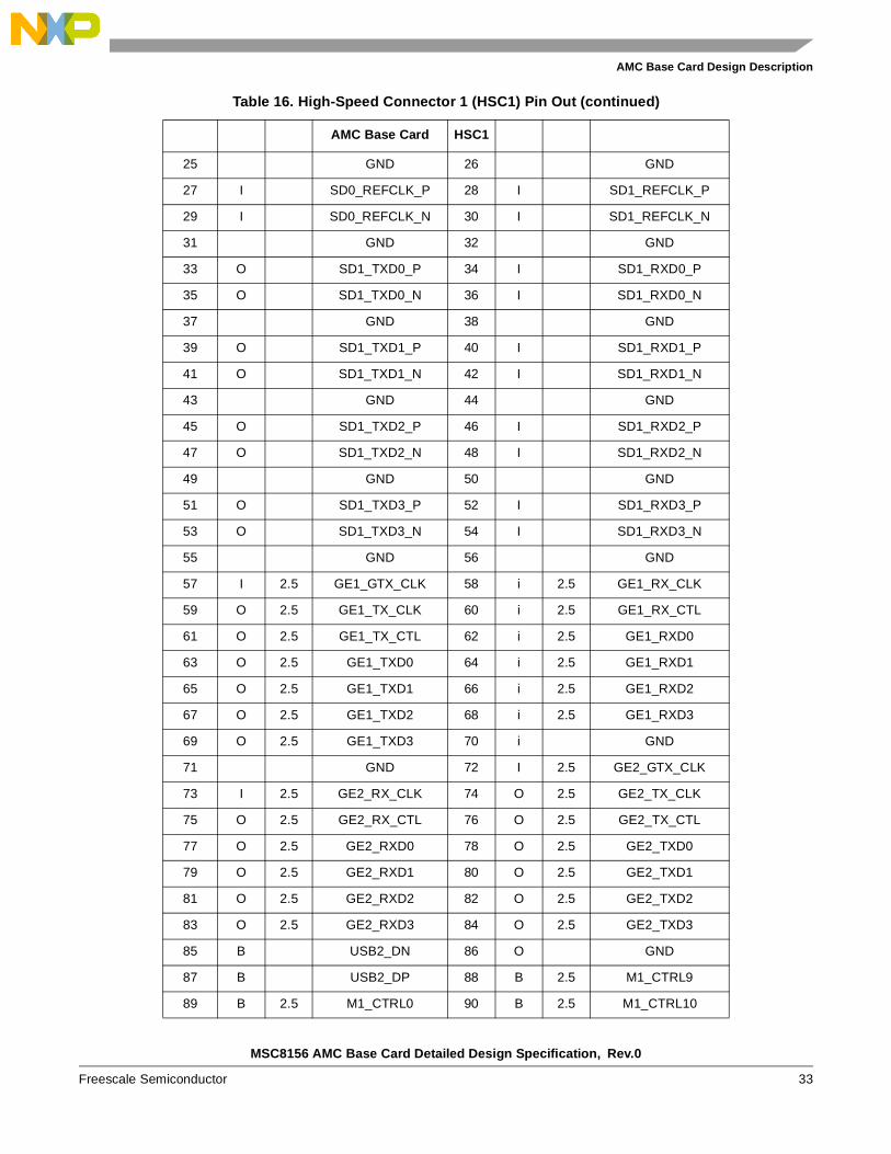
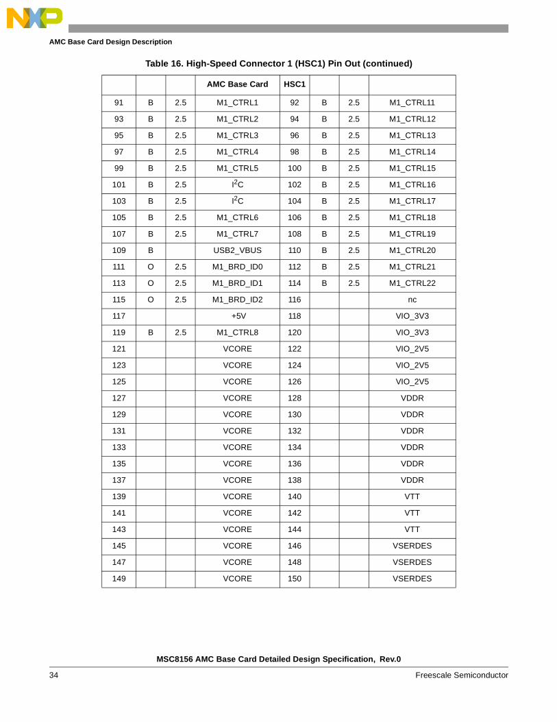
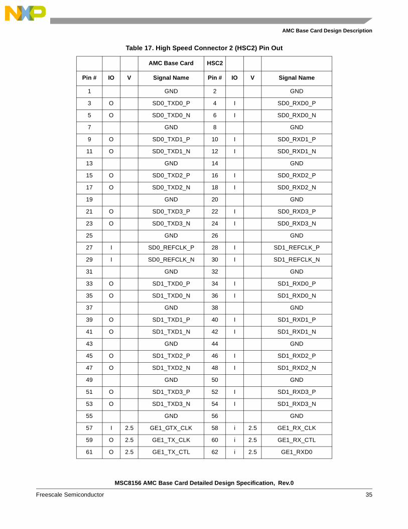
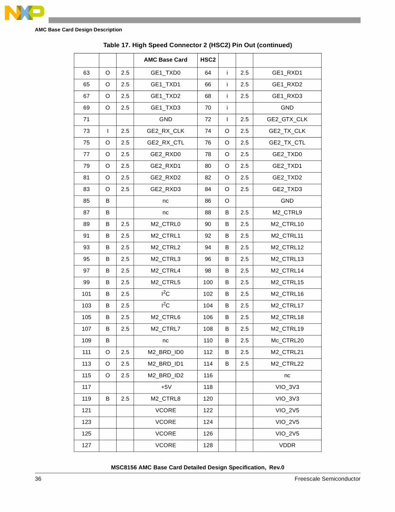
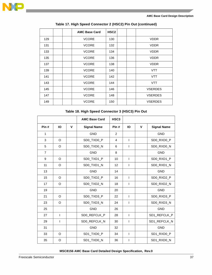
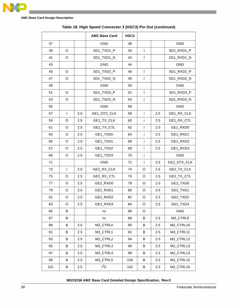
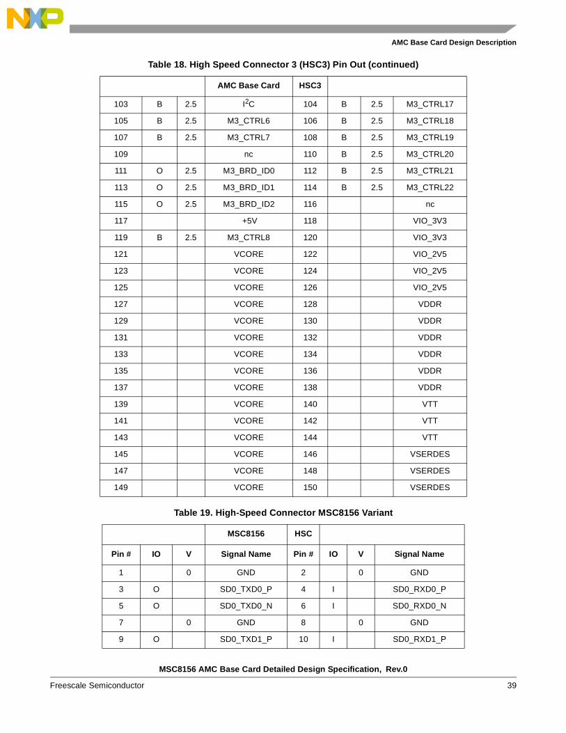
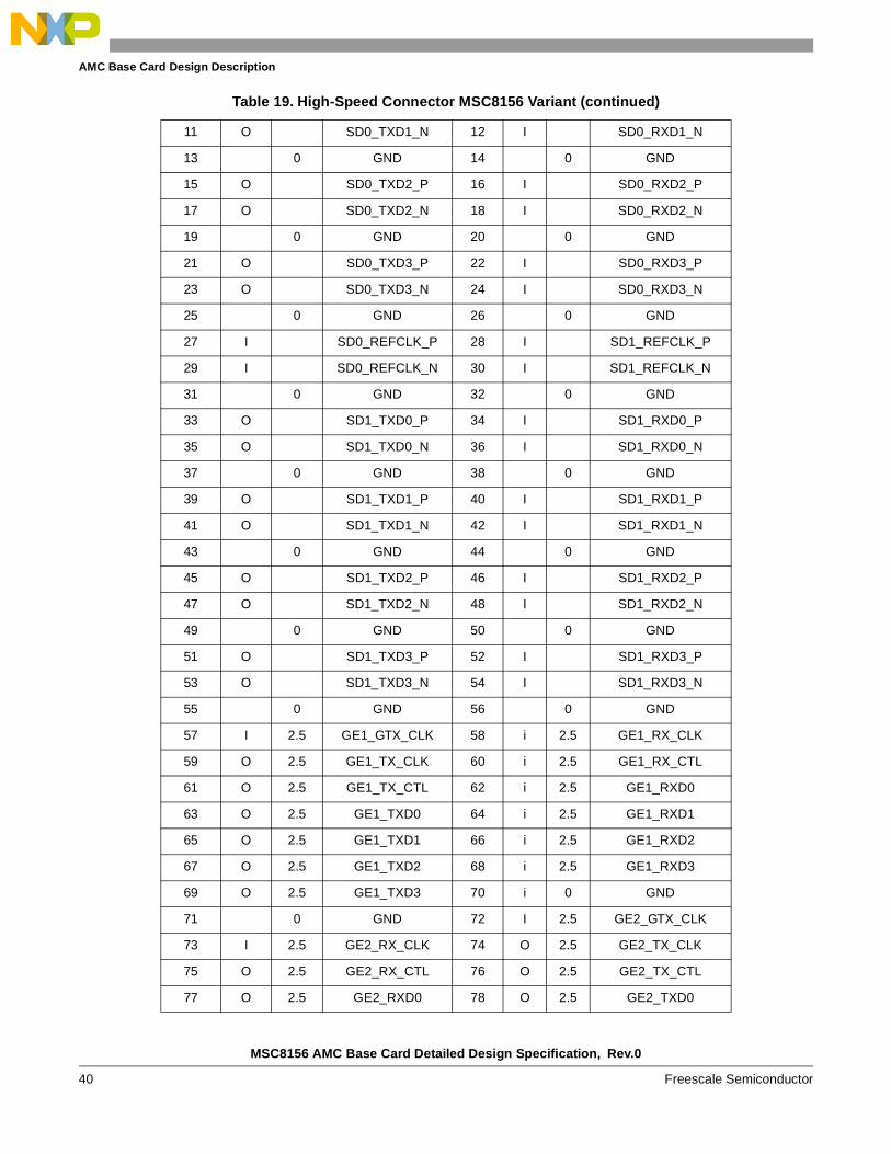
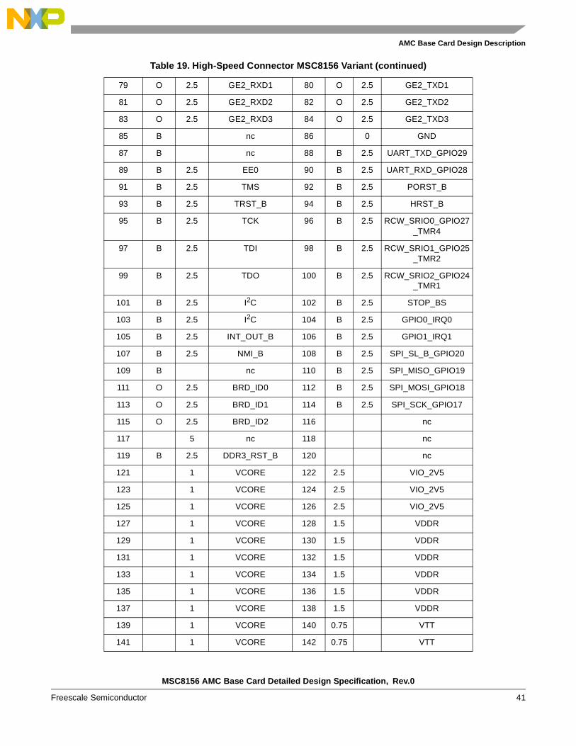
The generic signals, Mx_CTRL[0:22], connect direct to the FPGA enabling their usage to be adapted to a particular mezzanine. Table 16, Table 17, and Table 18 describe the HSC pin with their generic names. Each of the three MSC8156 mezzanine tiles connectors uses an identical pin out as described in Table 19. This table describes the actual signals names as is frequently referred to in this document.
Table 16. High-Speed Connector 1 (HSC1) Pin Out
AMC Base Card HSC1
Pin # IO V Signal Name Pin # IO V Signal Name
1 GND 2 GND
3 O SD0_TXD0_P 4 I SD0_RXD0_P
5 O SD0_TXD0_N 6 I SD0_RXD0_N
7 GND 8 GND
9 O SD0_TXD1_P 10 I SD0_RXD1_P
11 O SD0_TXD1_N 12 I SD0_RXD1_N
13 GND 14 GND
15 O SD0_TXD2_P 16 I SD0_RXD2_P
17 O SD0_TXD2_N 18 I SD0_RXD2_N
19 GND 20 GND
21 O SD0_TXD3_P 22 I SD0_RXD3_P
23 O SD0_TXD3_N 24 I SD0_RXD3_N
FPGA
Mezzanine 1
M1_CTRL[0:22]HSC1
SERDES
ETHERNET
Power
Mezzanine 2
M1_CTRL[0:22]HSC2
SERDES
ETHERNET
Power
Mezzanine 2
M1_CTRL[0:22]HSC3
SERDES
ETHERNET
Power
MSC8156 AMC Base Card Detailed Design Specification, Rev.0
Freescale Semiconductor 33
AMC Base Card Design Description
25 GND 26 GND
27 I SD0_REFCLK_P 28 I SD1_REFCLK_P
29 I SD0_REFCLK_N 30 I SD1_REFCLK_N
31 GND 32 GND
33 O SD1_TXD0_P 34 I SD1_RXD0_P
35 O SD1_TXD0_N 36 I SD1_RXD0_N
37 GND 38 GND
39 O SD1_TXD1_P 40 I SD1_RXD1_P
41 O SD1_TXD1_N 42 I SD1_RXD1_N
43 GND 44 GND
45 O SD1_TXD2_P 46 I SD1_RXD2_P
47 O SD1_TXD2_N 48 I SD1_RXD2_N
49 GND 50 GND
51 O SD1_TXD3_P 52 I SD1_RXD3_P
53 O SD1_TXD3_N 54 I SD1_RXD3_N
55 GND 56 GND
57 I 2.5 GE1_GTX_CLK 58 i 2.5 GE1_RX_CLK
59 O 2.5 GE1_TX_CLK 60 i 2.5 GE1_RX_CTL
61 O 2.5 GE1_TX_CTL 62 i 2.5 GE1_RXD0
63 O 2.5 GE1_TXD0 64 i 2.5 GE1_RXD1
65 O 2.5 GE1_TXD1 66 i 2.5 GE1_RXD2
67 O 2.5 GE1_TXD2 68 i 2.5 GE1_RXD3
69 O 2.5 GE1_TXD3 70 i GND
71 GND 72 I 2.5 GE2_GTX_CLK
73 I 2.5 GE2_RX_CLK 74 O 2.5 GE2_TX_CLK
75 O 2.5 GE2_RX_CTL 76 O 2.5 GE2_TX_CTL
77 O 2.5 GE2_RXD0 78 O 2.5 GE2_TXD0
79 O 2.5 GE2_RXD1 80 O 2.5 GE2_TXD1
81 O 2.5 GE2_RXD2 82 O 2.5 GE2_TXD2
83 O 2.5 GE2_RXD3 84 O 2.5 GE2_TXD3
85 B USB2_DN 86 O GND
87 B USB2_DP 88 B 2.5 M1_CTRL9
89 B 2.5 M1_CTRL0 90 B 2.5 M1_CTRL10
Table 16. High-Speed Connector 1 (HSC1) Pin Out (continued)
AMC Base Card HSC1
MSC8156 AMC Base Card Detailed Design Specification, Rev.0
34 Freescale Semiconductor
AMC Base Card Design Description
91 B 2.5 M1_CTRL1 92 B 2.5 M1_CTRL11
93 B 2.5 M1_CTRL2 94 B 2.5 M1_CTRL12
95 B 2.5 M1_CTRL3 96 B 2.5 M1_CTRL13
97 B 2.5 M1_CTRL4 98 B 2.5 M1_CTRL14
99 B 2.5 M1_CTRL5 100 B 2.5 M1_CTRL15
101 B 2.5 I2C 102 B 2.5 M1_CTRL16
103 B 2.5 I2C 104 B 2.5 M1_CTRL17
105 B 2.5 M1_CTRL6 106 B 2.5 M1_CTRL18
107 B 2.5 M1_CTRL7 108 B 2.5 M1_CTRL19
109 B USB2_VBUS 110 B 2.5 M1_CTRL20
111 O 2.5 M1_BRD_ID0 112 B 2.5 M1_CTRL21
113 O 2.5 M1_BRD_ID1 114 B 2.5 M1_CTRL22
115 O 2.5 M1_BRD_ID2 116 nc
117 +5V 118 VIO_3V3
119 B 2.5 M1_CTRL8 120 VIO_3V3
121 VCORE 122 VIO_2V5
123 VCORE 124 VIO_2V5
125 VCORE 126 VIO_2V5
127 VCORE 128 VDDR
129 VCORE 130 VDDR
131 VCORE 132 VDDR
133 VCORE 134 VDDR
135 VCORE 136 VDDR
137 VCORE 138 VDDR
139 VCORE 140 VTT
141 VCORE 142 VTT
143 VCORE 144 VTT
145 VCORE 146 VSERDES
147 VCORE 148 VSERDES
149 VCORE 150 VSERDES
Table 16. High-Speed Connector 1 (HSC1) Pin Out (continued)
AMC Base Card HSC1
MSC8156 AMC Base Card Detailed Design Specification, Rev.0
Freescale Semiconductor 35
AMC Base Card Design Description
Table 17. High Speed Connector 2 (HSC2) Pin Out
AMC Base Card HSC2
Pin # IO V Signal Name Pin # IO V Signal Name
1 GND 2 GND
3 O SD0_TXD0_P 4 I SD0_RXD0_P
5 O SD0_TXD0_N 6 I SD0_RXD0_N
7 GND 8 GND
9 O SD0_TXD1_P 10 I SD0_RXD1_P
11 O SD0_TXD1_N 12 I SD0_RXD1_N
13 GND 14 GND
15 O SD0_TXD2_P 16 I SD0_RXD2_P
17 O SD0_TXD2_N 18 I SD0_RXD2_N
19 GND 20 GND
21 O SD0_TXD3_P 22 I SD0_RXD3_P
23 O SD0_TXD3_N 24 I SD0_RXD3_N
25 GND 26 GND
27 I SD0_REFCLK_P 28 I SD1_REFCLK_P
29 I SD0_REFCLK_N 30 I SD1_REFCLK_N
31 GND 32 GND
33 O SD1_TXD0_P 34 I SD1_RXD0_P
35 O SD1_TXD0_N 36 I SD1_RXD0_N
37 GND 38 GND
39 O SD1_TXD1_P 40 I SD1_RXD1_P
41 O SD1_TXD1_N 42 I SD1_RXD1_N
43 GND 44 GND
45 O SD1_TXD2_P 46 I SD1_RXD2_P
47 O SD1_TXD2_N 48 I SD1_RXD2_N
49 GND 50 GND
51 O SD1_TXD3_P 52 I SD1_RXD3_P
53 O SD1_TXD3_N 54 I SD1_RXD3_N
55 GND 56 GND
57 I 2.5 GE1_GTX_CLK 58 i 2.5 GE1_RX_CLK
59 O 2.5 GE1_TX_CLK 60 i 2.5 GE1_RX_CTL
61 O 2.5 GE1_TX_CTL 62 i 2.5 GE1_RXD0
MSC8156 AMC Base Card Detailed Design Specification, Rev.0
36 Freescale Semiconductor
AMC Base Card Design Description
63 O 2.5 GE1_TXD0 64 i 2.5 GE1_RXD1
65 O 2.5 GE1_TXD1 66 i 2.5 GE1_RXD2
67 O 2.5 GE1_TXD2 68 i 2.5 GE1_RXD3
69 O 2.5 GE1_TXD3 70 i GND
71 GND 72 I 2.5 GE2_GTX_CLK
73 I 2.5 GE2_RX_CLK 74 O 2.5 GE2_TX_CLK
75 O 2.5 GE2_RX_CTL 76 O 2.5 GE2_TX_CTL
77 O 2.5 GE2_RXD0 78 O 2.5 GE2_TXD0
79 O 2.5 GE2_RXD1 80 O 2.5 GE2_TXD1
81 O 2.5 GE2_RXD2 82 O 2.5 GE2_TXD2
83 O 2.5 GE2_RXD3 84 O 2.5 GE2_TXD3
85 B nc 86 O GND
87 B nc 88 B 2.5 M2_CTRL9
89 B 2.5 M2_CTRL0 90 B 2.5 M2_CTRL10
91 B 2.5 M2_CTRL1 92 B 2.5 M2_CTRL11
93 B 2.5 M2_CTRL2 94 B 2.5 M2_CTRL12
95 B 2.5 M2_CTRL3 96 B 2.5 M2_CTRL13
97 B 2.5 M2_CTRL4 98 B 2.5 M2_CTRL14
99 B 2.5 M2_CTRL5 100 B 2.5 M2_CTRL15
101 B 2.5 I2C 102 B 2.5 M2_CTRL16
103 B 2.5 I2C 104 B 2.5 M2_CTRL17
105 B 2.5 M2_CTRL6 106 B 2.5 M2_CTRL18
107 B 2.5 M2_CTRL7 108 B 2.5 M2_CTRL19
109 B nc 110 B 2.5 Mc_CTRL20
111 O 2.5 M2_BRD_ID0 112 B 2.5 M2_CTRL21
113 O 2.5 M2_BRD_ID1 114 B 2.5 M2_CTRL22
115 O 2.5 M2_BRD_ID2 116 nc
117 +5V 118 VIO_3V3
119 B 2.5 M2_CTRL8 120 VIO_3V3
121 VCORE 122 VIO_2V5
123 VCORE 124 VIO_2V5
125 VCORE 126 VIO_2V5
127 VCORE 128 VDDR
Table 17. High Speed Connector 2 (HSC2) Pin Out (continued)
AMC Base Card HSC2
MSC8156 AMC Base Card Detailed Design Specification, Rev.0
Freescale Semiconductor 37
AMC Base Card Design Description
129 VCORE 130 VDDR
131 VCORE 132 VDDR
133 VCORE 134 VDDR
135 VCORE 136 VDDR
137 VCORE 138 VDDR
139 VCORE 140 VTT
141 VCORE 142 VTT
143 VCORE 144 VTT
145 VCORE 146 VSERDES
147 VCORE 148 VSERDES
149 VCORE 150 VSERDES
Table 18. High Speed Connector 3 (HSC3) Pin Out
AMC Base Card HSC3
Pin # IO V Signal Name Pin # IO V Signal Name
1 GND 2 GND
3 O SD0_TXD0_P 4 I SD0_RXD0_P
5 O SD0_TXD0_N 6 I SD0_RXD0_N
7 GND 8 GND
9 O SD0_TXD1_P 10 I SD0_RXD1_P
11 O SD0_TXD1_N 12 I SD0_RXD1_N
13 GND 14 GND
15 O SD0_TXD2_P 16 I SD0_RXD2_P
17 O SD0_TXD2_N 18 I SD0_RXD2_N
19 GND 20 GND
21 O SD0_TXD3_P 22 I SD0_RXD3_P
23 O SD0_TXD3_N 24 I SD0_RXD3_N
25 GND 26 GND
27 I SD0_REFCLK_P 28 I SD1_REFCLK_P
29 I SD0_REFCLK_N 30 I SD1_REFCLK_N
31 GND 32 GND
33 O SD1_TXD0_P 34 I SD1_RXD0_P
35 O SD1_TXD0_N 36 I SD1_RXD0_N
Table 17. High Speed Connector 2 (HSC2) Pin Out (continued)
AMC Base Card HSC2
MSC8156 AMC Base Card Detailed Design Specification, Rev.0
38 Freescale Semiconductor
AMC Base Card Design Description
37 GND 38 GND
39 O SD1_TXD1_P 40 I SD1_RXD1_P
41 O SD1_TXD1_N 42 I SD1_RXD1_N
43 GND 44 GND
45 O SD1_TXD2_P 46 I SD1_RXD2_P
47 O SD1_TXD2_N 48 I SD1_RXD2_N
49 GND 50 GND
51 O SD1_TXD3_P 52 I SD1_RXD3_P
53 O SD1_TXD3_N 54 I SD1_RXD3_N
55 GND 56 GND
57 I 2.5 GE1_GTX_CLK 58 i 2.5 GE1_RX_CLK
59 O 2.5 GE1_TX_CLK 60 i 2.5 GE1_RX_CTL
61 O 2.5 GE1_TX_CTL 62 i 2.5 GE1_RXD0
63 O 2.5 GE1_TXD0 64 i 2.5 GE1_RXD1
65 O 2.5 GE1_TXD1 66 i 2.5 GE1_RXD2
67 O 2.5 GE1_TXD2 68 i 2.5 GE1_RXD3
69 O 2.5 GE1_TXD3 70 i GND
71 GND 72 I 2.5 GE2_GTX_CLK
73 I 2.5 GE2_RX_CLK 74 O 2.5 GE2_TX_CLK
75 O 2.5 GE2_RX_CTL 76 O 2.5 GE2_TX_CTL
77 O 2.5 GE2_RXD0 78 O 2.5 GE2_TXD0
79 O 2.5 GE2_RXD1 80 O 2.5 GE2_TXD1
81 O 2.5 GE2_RXD2 82 O 2.5 GE2_TXD2
83 O 2.5 GE2_RXD3 84 O 2.5 GE2_TXD3
85 B nc 86 O GND
87 B nc 88 B 2.5 M3_CTRL9
89 B 2.5 M3_CTRL0 90 B 2.5 M3_CTRL10
91 B 2.5 M3_CTRL1 92 B 2.5 M3_CTRL11
93 B 2.5 M3_CTRL2 94 B 2.5 M3_CTRL12
95 B 2.5 M3_CTRL3 96 B 2.5 M3_CTRL13
97 B 2.5 M3_CTRL4 98 B 2.5 M3_CTRL14
99 B 2.5 M3_CTRL5 100 B 2.5 M3_CTRL15
101 B 2.5 I2C 102 B 2.5 M3_CTRL16
Table 18. High Speed Connector 3 (HSC3) Pin Out (continued)
AMC Base Card HSC3
MSC8156 AMC Base Card Detailed Design Specification, Rev.0
Freescale Semiconductor 39
AMC Base Card Design Description
103 B 2.5 I2C 104 B 2.5 M3_CTRL17
105 B 2.5 M3_CTRL6 106 B 2.5 M3_CTRL18
107 B 2.5 M3_CTRL7 108 B 2.5 M3_CTRL19
109 nc 110 B 2.5 M3_CTRL20
111 O 2.5 M3_BRD_ID0 112 B 2.5 M3_CTRL21
113 O 2.5 M3_BRD_ID1 114 B 2.5 M3_CTRL22
115 O 2.5 M3_BRD_ID2 116 nc
117 +5V 118 VIO_3V3
119 B 2.5 M3_CTRL8 120 VIO_3V3
121 VCORE 122 VIO_2V5
123 VCORE 124 VIO_2V5
125 VCORE 126 VIO_2V5
127 VCORE 128 VDDR
129 VCORE 130 VDDR
131 VCORE 132 VDDR
133 VCORE 134 VDDR
135 VCORE 136 VDDR
137 VCORE 138 VDDR
139 VCORE 140 VTT
141 VCORE 142 VTT
143 VCORE 144 VTT
145 VCORE 146 VSERDES
147 VCORE 148 VSERDES
149 VCORE 150 VSERDES
Table 19. High-Speed Connector MSC8156 Variant
MSC8156 HSC
Pin # IO V Signal Name Pin # IO V Signal Name
1 0 GND 2 0 GND
3 O SD0_TXD0_P 4 I SD0_RXD0_P
5 O SD0_TXD0_N 6 I SD0_RXD0_N
7 0 GND 8 0 GND
9 O SD0_TXD1_P 10 I SD0_RXD1_P
Table 18. High Speed Connector 3 (HSC3) Pin Out (continued)
AMC Base Card HSC3
MSC8156 AMC Base Card Detailed Design Specification, Rev.0
40 Freescale Semiconductor
AMC Base Card Design Description
11 O SD0_TXD1_N 12 I SD0_RXD1_N
13 0 GND 14 0 GND
15 O SD0_TXD2_P 16 I SD0_RXD2_P
17 O SD0_TXD2_N 18 I SD0_RXD2_N
19 0 GND 20 0 GND
21 O SD0_TXD3_P 22 I SD0_RXD3_P
23 O SD0_TXD3_N 24 I SD0_RXD3_N
25 0 GND 26 0 GND
27 I SD0_REFCLK_P 28 I SD1_REFCLK_P
29 I SD0_REFCLK_N 30 I SD1_REFCLK_N
31 0 GND 32 0 GND
33 O SD1_TXD0_P 34 I SD1_RXD0_P
35 O SD1_TXD0_N 36 I SD1_RXD0_N
37 0 GND 38 0 GND
39 O SD1_TXD1_P 40 I SD1_RXD1_P
41 O SD1_TXD1_N 42 I SD1_RXD1_N
43 0 GND 44 0 GND
45 O SD1_TXD2_P 46 I SD1_RXD2_P
47 O SD1_TXD2_N 48 I SD1_RXD2_N
49 0 GND 50 0 GND
51 O SD1_TXD3_P 52 I SD1_RXD3_P
53 O SD1_TXD3_N 54 I SD1_RXD3_N
55 0 GND 56 0 GND
57 I 2.5 GE1_GTX_CLK 58 i 2.5 GE1_RX_CLK
59 O 2.5 GE1_TX_CLK 60 i 2.5 GE1_RX_CTL
61 O 2.5 GE1_TX_CTL 62 i 2.5 GE1_RXD0
63 O 2.5 GE1_TXD0 64 i 2.5 GE1_RXD1
65 O 2.5 GE1_TXD1 66 i 2.5 GE1_RXD2
67 O 2.5 GE1_TXD2 68 i 2.5 GE1_RXD3
69 O 2.5 GE1_TXD3 70 i 0 GND
71 0 GND 72 I 2.5 GE2_GTX_CLK
73 I 2.5 GE2_RX_CLK 74 O 2.5 GE2_TX_CLK
75 O 2.5 GE2_RX_CTL 76 O 2.5 GE2_TX_CTL
77 O 2.5 GE2_RXD0 78 O 2.5 GE2_TXD0
Table 19. High-Speed Connector MSC8156 Variant (continued)
MSC8156 AMC Base Card Detailed Design Specification, Rev.0
Freescale Semiconductor 41
AMC Base Card Design Description
79 O 2.5 GE2_RXD1 80 O 2.5 GE2_TXD1
81 O 2.5 GE2_RXD2 82 O 2.5 GE2_TXD2
83 O 2.5 GE2_RXD3 84 O 2.5 GE2_TXD3
85 B nc 86 0 GND
87 B nc 88 B 2.5 UART_TXD_GPIO29
89 B 2.5 EE0 90 B 2.5 UART_RXD_GPIO28
91 B 2.5 TMS 92 B 2.5 PORST_B
93 B 2.5 TRST_B 94 B 2.5 HRST_B
95 B 2.5 TCK 96 B 2.5 RCW_SRIO0_GPIO27_TMR4
97 B 2.5 TDI 98 B 2.5 RCW_SRIO1_GPIO25_TMR2
99 B 2.5 TDO 100 B 2.5 RCW_SRIO2_GPIO24_TMR1
101 B 2.5 I2C 102 B 2.5 STOP_BS
103 B 2.5 I2C 104 B 2.5 GPIO0_IRQ0
105 B 2.5 INT_OUT_B 106 B 2.5 GPIO1_IRQ1
107 B 2.5 NMI_B 108 B 2.5 SPI_SL_B_GPIO20
109 B nc 110 B 2.5 SPI_MISO_GPIO19
111 O 2.5 BRD_ID0 112 B 2.5 SPI_MOSI_GPIO18
113 O 2.5 BRD_ID1 114 B 2.5 SPI_SCK_GPIO17
115 O 2.5 BRD_ID2 116 nc
117 5 nc 118 nc
119 B 2.5 DDR3_RST_B 120 nc
121 1 VCORE 122 2.5 VIO_2V5
123 1 VCORE 124 2.5 VIO_2V5
125 1 VCORE 126 2.5 VIO_2V5
127 1 VCORE 128 1.5 VDDR
129 1 VCORE 130 1.5 VDDR
131 1 VCORE 132 1.5 VDDR
133 1 VCORE 134 1.5 VDDR
135 1 VCORE 136 1.5 VDDR
137 1 VCORE 138 1.5 VDDR
139 1 VCORE 140 0.75 VTT
141 1 VCORE 142 0.75 VTT
Table 19. High-Speed Connector MSC8156 Variant (continued)
MSC8156 AMC Base Card Detailed Design Specification, Rev.0
42 Freescale Semiconductor
AMC Base Card Design Description
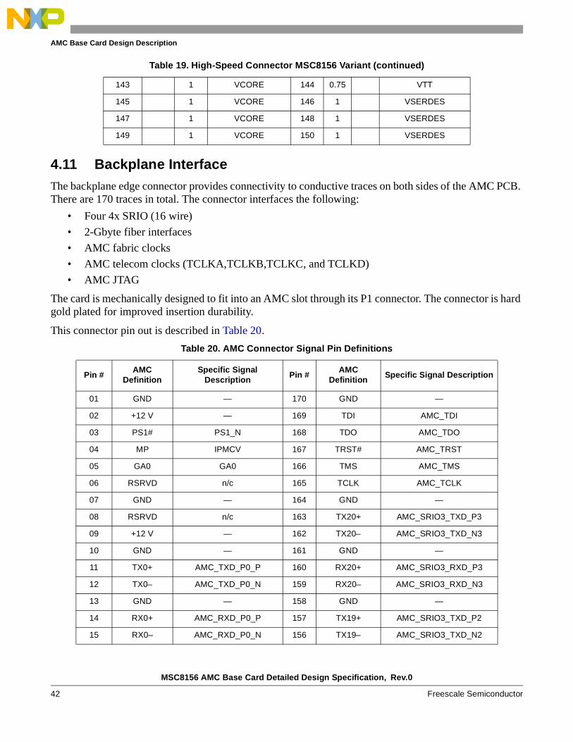
4.11 Backplane InterfaceThe backplane edge connector provides connectivity to conductive traces on both sides of the AMC PCB. There are 170 traces in total. The connector interfaces the following:
• Four 4x SRIO (16 wire)
• 2-Gbyte fiber interfaces
• AMC fabric clocks
• AMC telecom clocks (TCLKA,TCLKB,TCLKC, and TCLKD)
• AMC JTAG
The card is mechanically designed to fit into an AMC slot through its P1 connector. The connector is hard gold plated for improved insertion durability.
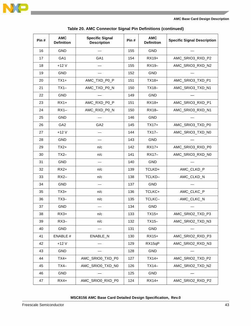
This connector pin out is described in Table 20.
143 1 VCORE 144 0.75 VTT
145 1 VCORE 146 1 VSERDES
147 1 VCORE 148 1 VSERDES
149 1 VCORE 150 1 VSERDES
Table 20. AMC Connector Signal Pin Definitions
Pin #AMC
DefinitionSpecific Signal
Description Pin #AMC
Definition Specific Signal Description
01 GND — 170 GND —
02 +12 V — 169 TDI AMC_TDI
03 PS1# PS1_N 168 TDO AMC_TDO
04 MP IPMCV 167 TRST# AMC_TRST
05 GA0 GA0 166 TMS AMC_TMS
06 RSRVD n/c 165 TCLK AMC_TCLK
07 GND — 164 GND —
08 RSRVD n/c 163 TX20+ AMC_SRIO3_TXD_P3
09 +12 V — 162 TX20– AMC_SRIO3_TXD_N3
10 GND — 161 GND —
11 TX0+ AMC_TXD_P0_P 160 RX20+ AMC_SRIO3_RXD_P3
12 TX0– AMC_TXD_P0_N 159 RX20– AMC_SRIO3_RXD_N3
13 GND — 158 GND —
14 RX0+ AMC_RXD_P0_P 157 TX19+ AMC_SRIO3_TXD_P2
15 RX0– AMC_RXD_P0_N 156 TX19– AMC_SRIO3_TXD_N2
Table 19. High-Speed Connector MSC8156 Variant (continued)
MSC8156 AMC Base Card Detailed Design Specification, Rev.0
Freescale Semiconductor 43
AMC Base Card Design Description
16 GND — 155 GND —
17 GA1 GA1 154 RX19+ AMC_SRIO3_RXD_P2
18 +12 V — 155 RX19– AMC_SRIO3_RXD_N2
19 GND — 152 GND —
20 TX1+ AMC_TXD_P0_P 151 TX18+ AMC_SRIO3_TXD_P1
21 TX1– AMC_TXD_P0_N 150 TX18– AMC_SRIO3_TXD_N1
22 GND — 149 GND —
23 RX1+ AMC_RXD_P0_P 151 RX18+ AMC_SRIO3_RXD_P1
24 RX1– AMC_RXD_P0_N 150 RX18– AMC_SRIO3_RXD_N1
25 GND — 146 GND —
26 GA2 GA2 145 TX17+ AMC_SRIO3_TXD_P0
27 +12 V — 144 TX17– AMC_SRIO3_TXD_N0
28 GND — 143 GND —
29 TX2+ n/c 142 RX17+ AMC_SRIO3_RXD_P0
30 TX2– n/c 141 RX17– AMC_SRIO3_RXD_N0
31 GND — 140 GND —
32 RX2+ n/c 139 TCLKD+ AMC_CLKD_P
33 RX2– n/c 138 TCLKD– AMC_CLKD_N
34 GND — 137 GND —
35 TX3+ n/c 136 TCLKC+ AMC_CLKC_P
36 TX3– n/c 135 TCLKC– AMC_CLKC_N
37 GND — 134 GND —
38 RX3+ n/c 133 TX15+ AMC_SRIO2_TXD_P3
39 RX3– n/c 132 TX15– AMC_SRIO2_TXD_N3
40 GND — 131 GND —
41 ENABLE # ENABLE_N 130 RX15+ AMC_SRIO2_RXD_P3
42 +12 V — 129 RX15qP AMC_SRIO2_RXD_N3
43 GND — 128 GND —
44 TX4+ AMC_SRIO0_TXD_P0 127 TX14+ AMC_SRIO2_TXD_P2
45 TX4– AMC_SRIO0_TXD_N0 126 TX14– AMC_SRIO2_TXD_N2
46 GND — 125 GND —
47 RX4+ AMC_SRIO0_RXD_P0 124 RX14+ AMC_SRIO2_RXD_P2
Table 20. AMC Connector Signal Pin Definitions (continued)
Pin #AMC
DefinitionSpecific Signal
DescriptionPin #
AMC Definition
Specific Signal Description

MSC8156 AMC Base Card Detailed Design Specification, Rev.0
44 Freescale Semiconductor
AMC Base Card Design Description
48 RX4– AMC_SRIO0_RXD_N0 123 RX14– AMC_SRIO2_RXD_N2
49 GND — 122 GND —
50 TX5+ AMC_SRIO0_TXD_P1 121 TX13+ AMC_SRIO2_TXD_P1
51 TX5– AMC_SRIO0_TXD_N1 120 TX13– AMC_SRIO2_TXD_N1
52 GND — 119 GND —
53 RX5+ AMC_SRIO0_RXD_P1 118 RX13+ AMC_SRIO2_RXD_P1
54 RX5– AMC_SRIO0_RXD_N1 119 RX13– AMC_SRIO2_RXD_N1
55 GND — 116 GND —
56 SCL_L AMC_SCL 115 TX12+ AMC_SRIO2_TXD_P0
57 +12 V — 114 TX12– AMC_SRIO2_TXD_N0
58 GND — 113 GND —
59 TX6+ AMC_SRIO0_TXD_P2 112 RX12+ AMC_SRIO2_RXD_P0
60 TX6– AMC_SRIO0_TXD_N2 111 RX12– AMC_SRIO2_RXD_N0
61 GND — 110 GND —
62 RX6+ AMC_SRIO0_RXD_P2 109 TX11+ AMC_SRIO1_TXD_P3
63 RX6– AMC_SRIO_RXD_N2 108 TX11– AMC_SRIO1_TXD_N3
64 GND — 107 GND —
65 TX7+ AMC_SRIO0_TXD_P3 106 RX11+ AMC_SRIO1_RXD_P3
66 TX7– AMC_SRIO0_TXD_N3 105 RX11– AMC_SRIO1_RXD_N3
67 GND — 104 GND —
68 RX7+ AMC_SRIO0_RXD_P3 103 TX10+ AMC_SRIO1_TXD_P2
69 RX7– AMC_SRIO0_RXD_N3 102 TX10– AMC_SRIO1_TXD_N2
70 GND — 101 GND —
71 SDA_L AMC_SDA 100 RX10+ AMC_SRIO1_RXD_P2
72 +12 V — 99 RX10– AMC_SRIO1_RXD_N2
73 GND — 98 GND —
74 CLKA+ AMC_CLKA_P 97 TX9+ AMC_SRIO1_TXD_P1
75 CLKA– AMC_CLKA_N 96 TX9– AMC_SRIO1_TXD_N1
76 GND — 95 GND —
77 CLKB+ AMC_CLKB_P 94 RX9+ AMC_SRIO1_RXD_P1
78 CLKB– AMC_CLKB_N 93 RX9– AMC_SRIO1_RXD_N1
79 GND — 92 GND —
Table 20. AMC Connector Signal Pin Definitions (continued)
Pin #AMC
DefinitionSpecific Signal
DescriptionPin #
AMC Definition
Specific Signal Description
MSC8156 AMC Base Card Detailed Design Specification, Rev.0
Freescale Semiconductor 45
AMC Base Card Design Description
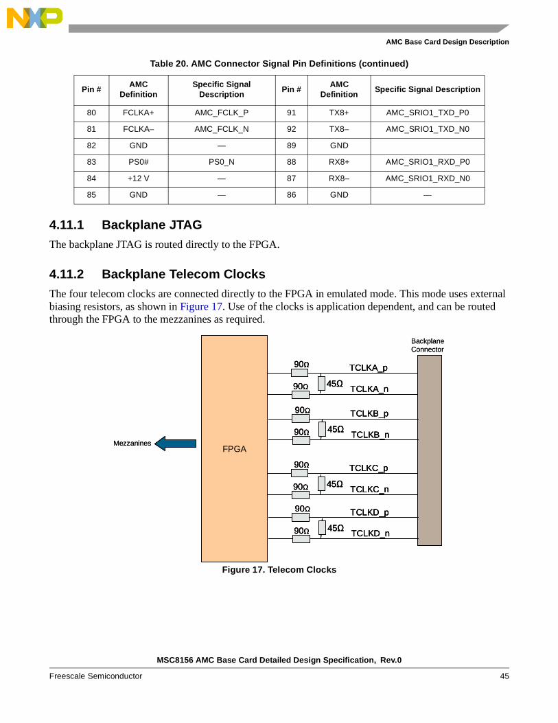
4.11.1 Backplane JTAGThe backplane JTAG is routed directly to the FPGA.
4.11.2 Backplane Telecom ClocksThe four telecom clocks are connected directly to the FPGA in emulated mode. This mode uses external biasing resistors, as shown in Figure 17. Use of the clocks is application dependent, and can be routed through the FPGA to the mezzanines as required.
Figure 17. Telecom Clocks
80 FCLKA+ AMC_FCLK_P 91 TX8+ AMC_SRIO1_TXD_P0
81 FCLKA– AMC_FCLK_N 92 TX8– AMC_SRIO1_TXD_N0
82 GND — 89 GND
83 PS0# PS0_N 88 RX8+ AMC_SRIO1_RXD_P0
84 +12 V — 87 RX8– AMC_SRIO1_RXD_N0
85 GND — 86 GND —
Table 20. AMC Connector Signal Pin Definitions (continued)
Pin #AMC
DefinitionSpecific Signal
DescriptionPin #
AMC Definition
Specific Signal Description
FPGA
90Ω
90Ω
TCLKA_p
TCLKA_n45Ω
90Ω
90Ω
TCLKB_p
TCLKB_n45Ω
90Ω
90Ω
TCLKC_p
TCLKC_n45Ω
90Ω
90Ω
TCLKD_p
TCLKD_n45Ω
BackplaneConnector
MezzaninesFPGA
90Ω
90Ω
TCLKA_p
TCLKA_n45Ω
90Ω
90Ω
TCLKA_p
TCLKA_n45Ω
90Ω
90Ω
TCLKB_p
TCLKB_n45Ω
90Ω
90Ω
TCLKB_p
TCLKB_n45Ω
90Ω
90Ω
TCLKC_p
TCLKC_n45Ω
90Ω
90Ω
TCLKC_p
TCLKC_n45Ω
90Ω
90Ω
TCLKD_p
TCLKD_n45Ω
90Ω
90Ω
TCLKD_p
TCLKD_n45Ω
BackplaneConnector
Mezzanines
MSC8156 AMC Base Card Detailed Design Specification, Rev.0
46 Freescale Semiconductor
AMC Base Card Design Description
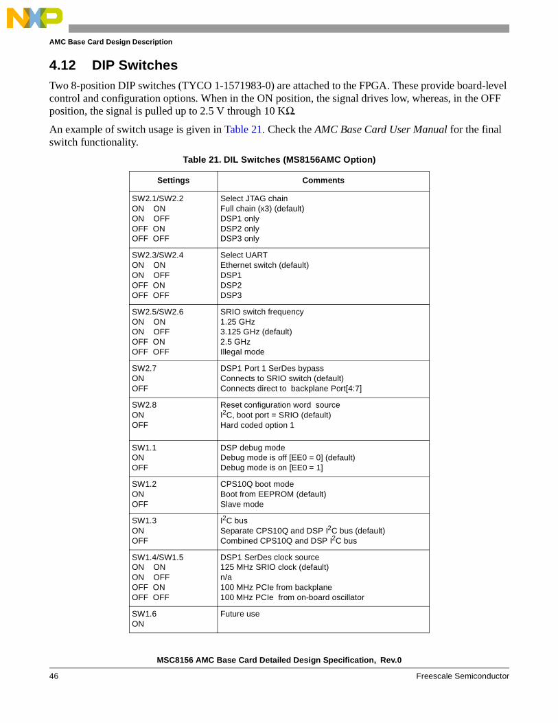
4.12 DIP SwitchesTwo 8-position DIP switches (TYCO 1-1571983-0) are attached to the FPGA. These provide board-level control and configuration options. When in the ON position, the signal drives low, whereas, in the OFF position, the signal is pulled up to 2.5 V through 10 KΩ.
An example of switch usage is given in Table 21. Check the AMC Base Card User Manual for the final switch functionality.
Table 21. DIL Switches (MS8156AMC Option)
Settings Comments
SW2.1/SW2.2ON ONON OFFOFF ONOFF OFF
Select JTAG chain Full chain (x3) (default)DSP1 onlyDSP2 onlyDSP3 only
SW2.3/SW2.4ON ONON OFFOFF ONOFF OFF
Select UART Ethernet switch (default)DSP1 DSP2 DSP3
SW2.5/SW2.6ON ONON OFFOFF ONOFF OFF
SRIO switch frequency1.25 GHz3.125 GHz (default)2.5 GHzIllegal mode
SW2.7ONOFF
DSP1 Port 1 SerDes bypassConnects to SRIO switch (default)Connects direct to backplane Port[4:7]
SW2.8ONOFF
Reset configuration word sourceI2C, boot port = SRIO (default)Hard coded option 1
SW1.1ONOFF
DSP debug modeDebug mode is off [EE0 = 0] (default)Debug mode is on [EE0 = 1]
SW1.2ONOFF
CPS10Q boot modeBoot from EEPROM (default)Slave mode
SW1.3ONOFF
I2C busSeparate CPS10Q and DSP I2C bus (default)Combined CPS10Q and DSP I2C bus
SW1.4/SW1.5ON ONON OFFOFF ONOFF OFF
DSP1 SerDes clock source125 MHz SRIO clock (default)n/a100 MHz PCIe from backplane100 MHz PCIe from on-board oscillator
SW1.6ON
Future use

MSC8156 AMC Base Card Detailed Design Specification, Rev.0
Freescale Semiconductor 47
AMC Base Card Design Description
4.13 LEDsA number of LEDs provide generic status information, as described in Table 22.
Refer the AMC Base Card User Manual for the final D1–D5 and Ethernet LED (J13, P3) functionality.
4.14 Push ButtonsThere are two push buttons on the AMC base card. These are:
• Board reset: This is connected to the FPGA and the MMC and recycles power. This is a miniature push button switch located on the front panel (that is, the Bourns 7914S-1-1000E 4-mm right-angle push button switch).
• Generic reset: This is a small, low-profile push button switch on the secondary side of the card, which is used as a development aid. This is connected to the FPGA, and by default, it resets the board (C and K Components KSR221GLFS switch).
SW1.7OFFON
Working configurationStand-alone mode xTCA chassis (default)
SW1.8ON
Future use
Table 22. LEDs
LED Color Comments
D7 Blue Hot swap LED (MMC)—located on front panel
D8 Red Out of service (MMC)—located on front panel
D9 Green In service (MMC)—located on front panel
J13 Green/Orange Located in integrated1 RJ45 /USB connector, controlled by LED_RJ45_D
P3 Green Located in second RJ45 (RHS), controlled by LED_RJ45_A through FPGA
P3 Green Located in second RJ45 (LHS), controlled by LED_RJ45_B through FPGA
D1 Green Connected direct to FPGA
D2 Green Connected direct to FPGA
D3 Green Connected direct to FPGA
D4 Yellow Connected direct to FPGA
D5 Yellow Connected direct to FPGA
D32 Yellow UART activity
Table 21. DIL Switches (MS8156AMC Option) (continued)
Settings Comments
MSC8156 AMC Base Card Detailed Design Specification, Rev.0
48 Freescale Semiconductor
AMC Base Card Design Description
4.15 Power SupplyThe following two separate power rail inputs to the card from the AMC connector:
• 3.3 V supplying 150 mA for board management
• 12 V supplying 60-W payload power
The required voltages for the card are generated locally on-board from the 12 V supply using DC–DC converters.
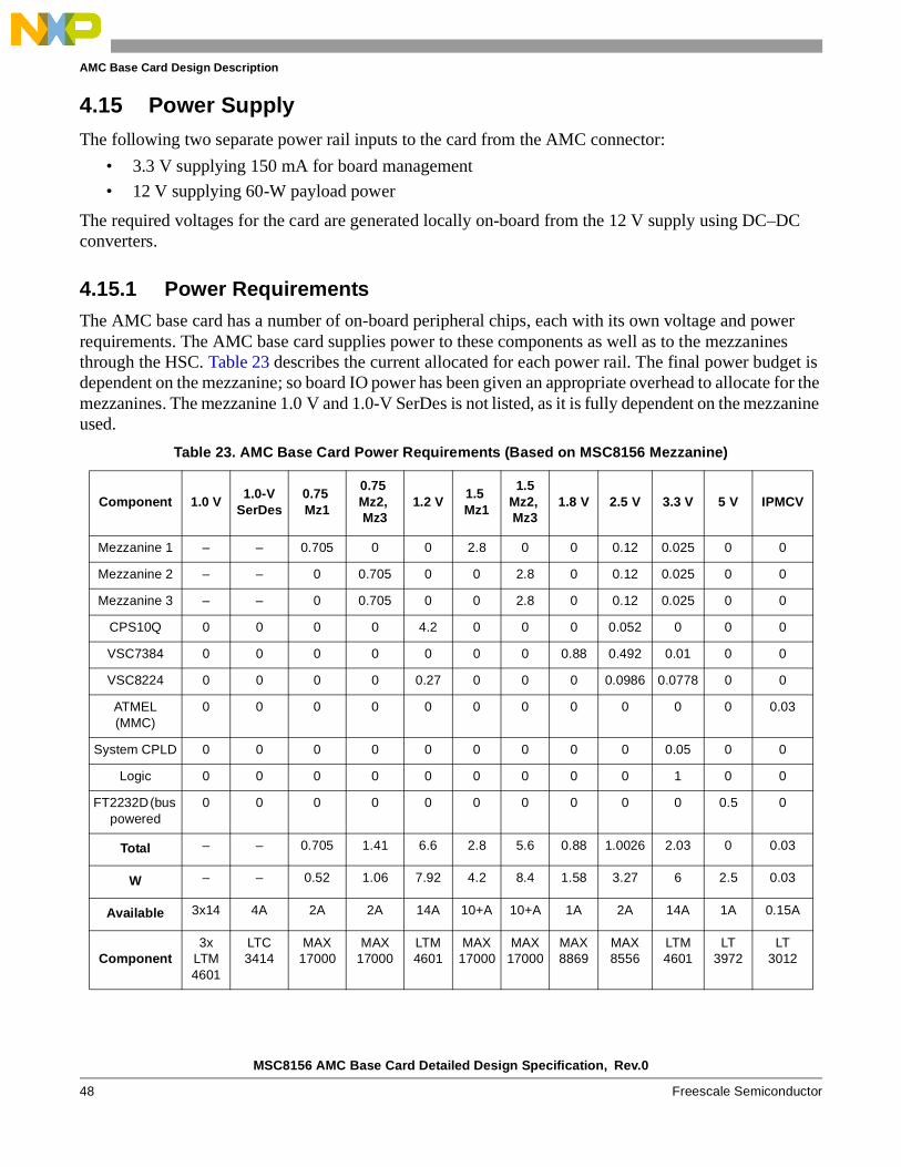
4.15.1 Power Requirements The AMC base card has a number of on-board peripheral chips, each with its own voltage and power requirements. The AMC base card supplies power to these components as well as to the mezzanines through the HSC. Table 23 describes the current allocated for each power rail. The final power budget is dependent on the mezzanine; so board IO power has been given an appropriate overhead to allocate for the mezzanines. The mezzanine 1.0 V and 1.0-V SerDes is not listed, as it is fully dependent on the mezzanine used.
Table 23. AMC Base Card Power Requirements (Based on MSC8156 Mezzanine)
Component 1.0 V1.0-V
SerDes0.75 Mz1
0.75 Mz2, Mz3
1.2 V1.5 Mz1
1.5Mz2, Mz3
1.8 V 2.5 V 3.3 V 5 V IPMCV
Mezzanine 1 – – 0.705 0 0 2.8 0 0 0.12 0.025 0 0
Mezzanine 2 – – 0 0.705 0 0 2.8 0 0.12 0.025 0 0
Mezzanine 3 – – 0 0.705 0 0 2.8 0 0.12 0.025 0 0
CPS10Q 0 0 0 0 4.2 0 0 0 0.052 0 0 0
VSC7384 0 0 0 0 0 0 0 0.88 0.492 0.01 0 0
VSC8224 0 0 0 0 0.27 0 0 0 0.0986 0.0778 0 0
ATMEL (MMC)
0 0 0 0 0 0 0 0 0 0 0 0.03
System CPLD 0 0 0 0 0 0 0 0 0 0.05 0 0
Logic 0 0 0 0 0 0 0 0 0 1 0 0
FT2232D (bus powered
0 0 0 0 0 0 0 0 0 0 0.5 0
Total – – 0.705 1.41 6.6 2.8 5.6 0.88 1.0026 2.03 0 0.03
W – – 0.52 1.06 7.92 4.2 8.4 1.58 3.27 6 2.5 0.03
Available 3x14 4A 2A 2A 14A 10+A 10+A 1A 2A 14A 1A 0.15A
Component3x
LTM4601
LTC3414
MAX17000
MAX17000
LTM4601
MAX17000
MAX17000
MAX8869
MAX8556
LTM4601
LT3972
LT3012

MSC8156 AMC Base Card Detailed Design Specification, Rev.0
Freescale Semiconductor 49
AMC Base Card Design Description
Figure 18. Power Architecture
4.15.1.1 Mezzanine Core Voltage Generation
Three linear LTM4601 power modules are used to supply core power to the three mezzanine connectors. This voltage can be adjusted through resistor changes to select from 0.8 to 1.2 V. By default, the core voltages are set to 1 V.
when Rset is 90.9 KW Eqn. 1
The voltage can be fine-tuned by the margining pins that are connected to the MMC.
The margining offset has been set to ±5% of Vout through the MPGM pin using the following equation:
Eqn. 2
The output margining is ± margining of this value, as described in Table 24.
Vout 0.6V60.4K Rset+
Rset------------------------------- 1.0V= =
Rpgm
Vout 1.18v 10K××0.6V Vout m inarg( )×---------------------------------------------- 393KΩ= =
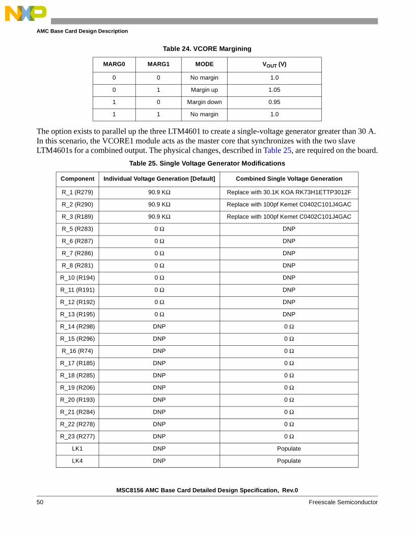
MSC8156 AMC Base Card Detailed Design Specification, Rev.0
50 Freescale Semiconductor
AMC Base Card Design Description
The option exists to parallel up the three LTM4601 to create a single-voltage generator greater than 30 A. In this scenario, the VCORE1 module acts as the master core that synchronizes with the two slave LTM4601s for a combined output. The physical changes, described in Table 25, are required on the board.
Table 24. VCORE Margining
MARG0 MARG1 MODE VOUT (V)
0 0 No margin 1.0
0 1 Margin up 1.05
1 0 Margin down 0.95
1 1 No margin 1.0
Table 25. Single Voltage Generator Modifications
Component Individual Voltage Generation [Default] Combined Single Voltage Generation
R_1 (R279) 90.9 KΩ Replace with 30.1K KOA RK73H1ETTP3012F
R_2 (R290) 90.9 KΩ Replace with 100pf Kemet C0402C101J4GAC
R_3 (R189) 90.9 KΩ Replace with 100pf Kemet C0402C101J4GAC
R_5 (R283) 0 Ω DNP
R_6 (R287) 0 Ω DNP
R_7 (R286) 0 Ω DNP
R_8 (R281) 0 Ω DNP
R_10 (R194) 0 Ω DNP
R_11 (R191) 0 Ω DNP
R_12 (R192) 0 Ω DNP
R_13 (R195) 0 Ω DNP
R_14 (R298) DNP 0 Ω
R_15 (R296) DNP 0 Ω
R_16 (R74) DNP 0 Ω
R_17 (R185) DNP 0 Ω
R_18 (R285) DNP 0 Ω
R_19 (R206) DNP 0 Ω
R_20 (R193) DNP 0 Ω
R_21 (R284) DNP 0 Ω
R_22 (R278) DNP 0 Ω
R_23 (R277) DNP 0 Ω
LK1 DNP Populate
LK4 DNP Populate

MSC8156 AMC Base Card Detailed Design Specification, Rev.0
Freescale Semiconductor 51
AMC Base Card Design Description
4.15.1.2 AMC Base Card Core and IO Voltages
The 3.3-V IO is generated from an LTM4601 that steps down from 12 to 3.3 V using the following equation:
when Rset is 13.3 KΩ Eqn. 3
The 3.3 V in turn feeds the 2.5, 1.8, and 1.0 V (SerDes) rails using MAX8526, MAX8869, and LTC3414 converters to step down.
The MAX8856 2.5 V is generated from:
when Rset1 = 4.02 KΩ and Rset2 = 1 KΩ Eqn. 4
The MAX8869 is a fixed 1.8 V.
The LTC3414 1.0 V is generated from:
when Rset2 = 200 KΩ and Rset1 = 806 KΩ Eqn. 5
The option exists to connect the SerDes voltage direct to the core voltage through LK2, 3, and 5 links. By default, these links are DNP.
4.15.1.3 DDR2/DDR3 Generation
Two MAX17000 generate the DDR voltage for the mezzanines. One MAX17000 generates the supply for the Mezzanine 1 position, while the second generates the supply for the Mezzanine 2 and 3 positions. The rationale behind this is to allow mezzanines to be populated with a combination of DDR2 and DDR3.
The MAX17000 devices are controlled from the MMC and can be programmed to generate DDR2 (1.8 V/0/9 V) or DDR3 (1.5 V/0.75 V) through the DDR_FB_R1 and DDR_FB_R2 control signals. By default, these are set to DDR3.
The MAX17000 requires 5-V supplies, which is supplied through the LT3972 step-down regulator. The 5 V is generated from the equation:
where R1set = 56 KΩ and R2set = 100 KΩ Eqn. 6
Vout 0.6V60.4K Rset+
Rset------------------------------- 3.3V= =
Vout 0.5V1 Rset1+
Rset2---------------------- 2.5V= =
Vout 0.8V1 Rset2+
Rset1---------------------- 1.0V= =
R1set R2set
Vout
0.79V-------------- 1–⎝ ⎠⎛ ⎞=
MSC8156 AMC Base Card Detailed Design Specification, Rev.0
52 Freescale Semiconductor
AMC Base Card Design Description
The LT3972 also supplies 5-V mezzanine IO (typically for USB applications).
4.15.1.4 Stand-Alone Operation
For stand-alone mode, a barrel connector supplies a single-filtered 12-V supply. In this mode (selectable through a switch), the 12 V is stepped down to 3.3 V to supply the IPMCV rail. By default, the power connector is a DNP.
Note that Freescale recommends running the AMC base card in an appropriate μTCA, ARCA, or picoTCA chassis to provide the appropriate power and cooling.
4.15.1.5 Power Sequence
The board power-up sequence is initiated by the MMC that controls the timing of the enable signals to the various DC–DC converters, as shown in Figure 19. The power-up sequence restrictions are described in Table 26.
’
To meet the requirements specified in Table 26, the following order is used:
VCORE1 ≥ VCORE2 ≥ VCORE3 ≥ 1V0 ≥ 1V8 ≥ 2V5 ≥ 3V3 ≥ 1V2 ≥ 1V5/0V75.
Table 26. Power Sequencing Requirements
Device Notes Sequence
MSC8156 Core voltage first, then IO in any order 1V0 then 2V5
FPGA No specific power-up optionsInternal power good signal generated from VCC (1V2) and VCCAUX (3V3) pins, so ensure 2V5 is not last supply up
2V5/3.3V then 1V2
CPS10Q No power sequence requirements –
VSC7384 VDD_OUT33 (3V3) VDD_IO25 (2V5) +1.35 VVDD_PLL (2V5) VDD_IO25 (2V5) +0.5 V
2V5 then 3V3
VSC8224 No power sequence requirements –
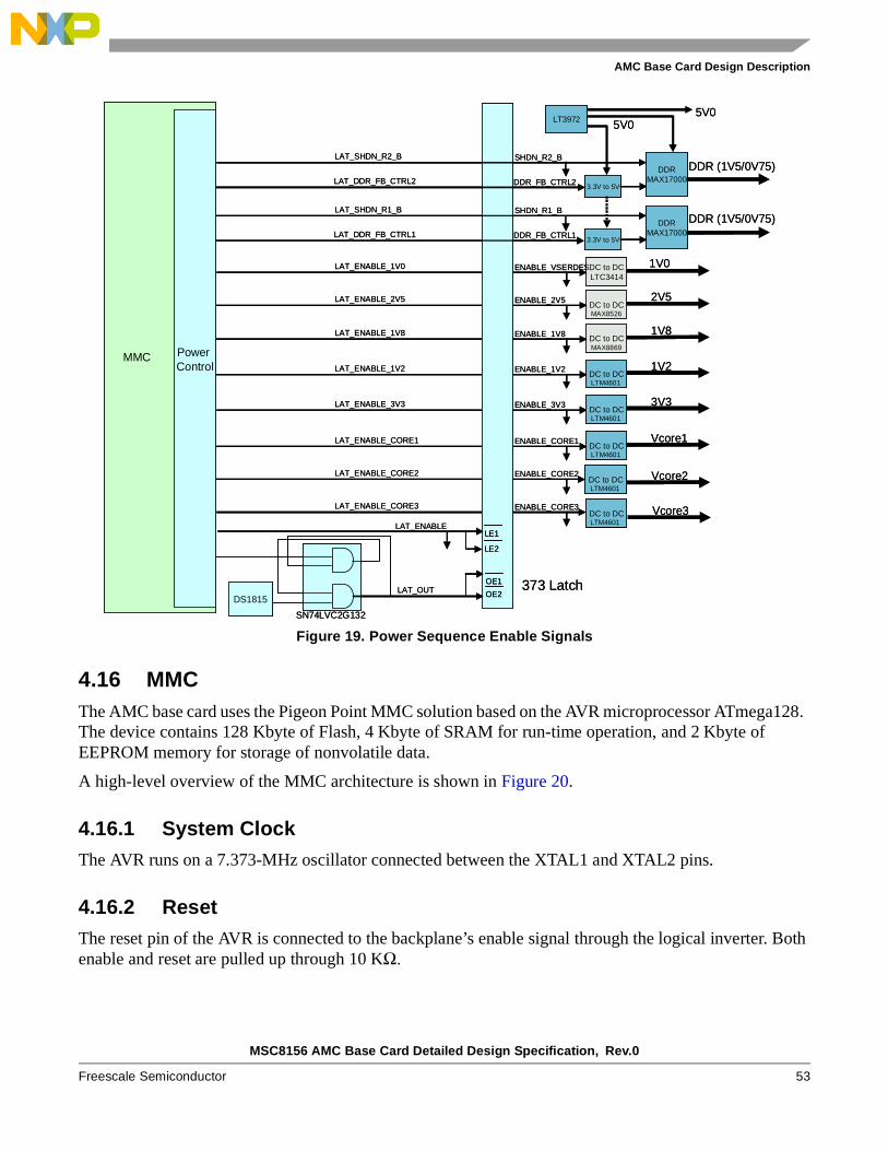
MSC8156 AMC Base Card Detailed Design Specification, Rev.0
Freescale Semiconductor 53
AMC Base Card Design Description
Figure 19. Power Sequence Enable Signals
4.16 MMCThe AMC base card uses the Pigeon Point MMC solution based on the AVR microprocessor ATmega128. The device contains 128 Kbyte of Flash, 4 Kbyte of SRAM for run-time operation, and 2 Kbyte of EEPROM memory for storage of nonvolatile data.
A high-level overview of the MMC architecture is shown in Figure 20.
4.16.1 System ClockThe AVR runs on a 7.373-MHz oscillator connected between the XTAL1 and XTAL2 pins.
4.16.2 ResetThe reset pin of the AVR is connected to the backplane’s enable signal through the logical inverter. Both enable and reset are pulled up through 10 KΩ.
DC to DC
DC to DCVcore1
DDR (1V5/0V75)
LTM4601
LTM4601
DC to DCLTM4601
LT3972
3.3V to 5V
Vcore2
Vcore3
373 Latch
ENABLE_CORE1LAT_ENABLE_CORE1
ENABLE_CORE2LAT_ENABLE_CORE2
ENABLE_CORE3LAT_ENABLE_CORE3
DC to DC3V3
LTM4601
ENABLE_3V3LAT_ENABLE_3V3
DC to DC1V2
LTM4601
ENABLE_1V2LAT_ENABLE_1V2
DC to DC1V8
MAX8869
ENABLE_1V8LAT_ENABLE_1V8
DC to DC2V5
MAX8526
ENABLE_2V5LAT_ENABLE_2V5
DC to DCLTC3414
1V0ENABLE_VSERDESLAT_ENABLE_1V0
DDRMAX17000
SHDN_R1_BLAT_SHDN_R1_B
DDR_FB_CTRL1LAT_DDR_FB_CTRL1
DDR (1V5/0V75)
3.3V to 5V
DDRMAX17000
SHDN_R2_BLAT_SHDN_R2_B
DDR_FB_CTRL2LAT_DDR_FB_CTRL2
5V0
LE1
LE2
Power Control
LAT_ENABLE
OE1
OE2DS1815
LAT_OUT
SN74LVC2G132
MMC
5V0
DC to DC
DC to DCVcore1
DDR (1V5/0V75)
LTM4601
LTM4601
DC to DCLTM4601DC to DCLTM4601
LT3972
3.3V to 5V
Vcore2
Vcore3
373 Latch
ENABLE_CORE1LAT_ENABLE_CORE1
ENABLE_CORE2LAT_ENABLE_CORE2
ENABLE_CORE3LAT_ENABLE_CORE3
DC to DC3V3
LTM4601
ENABLE_3V3LAT_ENABLE_3V3
DC to DC1V2
LTM4601
ENABLE_1V2LAT_ENABLE_1V2
DC to DC1V8
MAX8869
ENABLE_1V8LAT_ENABLE_1V8
DC to DC2V5
MAX8526
ENABLE_2V5LAT_ENABLE_2V5
DC to DCLTC3414
1V0ENABLE_VSERDESLAT_ENABLE_1V0
DDRMAX17000
SHDN_R1_BLAT_SHDN_R1_B
DDR_FB_CTRL1LAT_DDR_FB_CTRL1
DDR (1V5/0V75)
3.3V to 5V
DDRMAX17000
SHDN_R2_BLAT_SHDN_R2_B
DDR_FB_CTRL2LAT_DDR_FB_CTRL2
5V0
LE1LE1
LE2LE2
Power Control
LAT_ENABLE
OE1OE1
OE2OE2DS1815
LAT_OUT
SN74LVC2G132
MMC
5V0
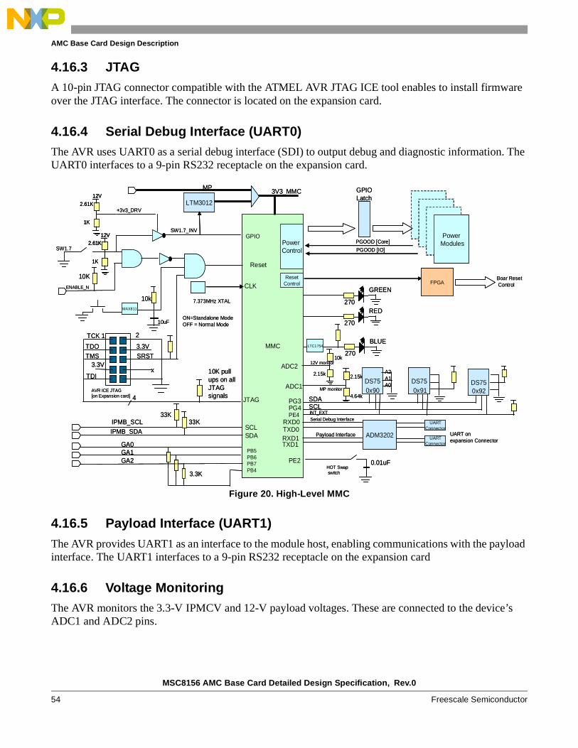
MSC8156 AMC Base Card Detailed Design Specification, Rev.0
54 Freescale Semiconductor
AMC Base Card Design Description
4.16.3 JTAGA 10-pin JTAG connector compatible with the ATMEL AVR JTAG ICE tool enables to install firmware over the JTAG interface. The connector is located on the expansion card.
4.16.4 Serial Debug Interface (UART0)The AVR uses UART0 as a serial debug interface (SDI) to output debug and diagnostic information. The UART0 interfaces to a 9-pin RS232 receptacle on the expansion card.
Figure 20. High-Level MMC
4.16.5 Payload Interface (UART1)
The AVR provides UART1 as an interface to the module host, enabling communications with the payload interface. The UART1 interfaces to a 9-pin RS232 receptacle on the expansion card
4.16.6 Voltage MonitoringThe AVR monitors the 3.3-V IPMCV and 12-V payload voltages. These are connected to the device’s ADC1 and ADC2 pins.
MMC
7.373MHz XTAL
ENABLE_N
SW1.7
CLK
Reset
ON=Standalone ModeOFF = Normal Mode
10k
10uF
1 2
TDO
TDIx
TMS3.3V
AVR ICE JTAG [on Expansion card]
3.3V
TCK
SRST
10K pull ups on all JTAG signals
JTAG
ADM3202
RXD0TXD0
UARTConnector
RXD1TXD1
Serial Debug Interface
Payload Interface
4
IPMB_SCLIPMB_SDA
33K33K
SCLSDA
PG3 SDAPG4 SCL
DS75 DS75
A2A1A0
0x90DS75
0x91 0x92
GA0GA1GA2
3.3K
PB5PB6PB7PB4
HOT Swapswitch
0.01uFPE2
BLUE
270
RED
270
GREEN
270
INT_EXTPE4
12V monitor
MP monitor
10k
2.15k 2.15k
4.64k
ADC2
ADC1
Power Control
LTM3012
3V3_MMCMP
GPIO
12V
2.61K
1K
GPIO Latch
PGOOD [Core]Power
Modules
LTC1754
MAX811
UARTConnector
UART on expansion Connector
PGOOD [IO]
ResetControl FPGA
Boar ResetControl
10K
+3v3_DRV
12V
2.61K
1K
SW1.7_INV
MMC
7.373MHz XTAL
ENABLE_N
SW1.7
CLK
Reset
ON=Standalone ModeOFF = Normal Mode
10k
10uF
1 2
TDO
TDIx
TMS3.3V
AVR ICE JTAG [on Expansion card]
3.3V
TCK
SRST
10K pull ups on all JTAG signals
JTAG
ADM3202
RXD0TXD0
UARTConnector
RXD1TXD1
Serial Debug Interface
Payload Interface
4
IPMB_SCLIPMB_SDA
33K33K
SCLSDA
PG3 SDAPG4 SCL
DS75 DS75
A2A1A0
0x90DS75
0x91 0x92
GA0GA1GA2
3.3K
PB5PB6PB7PB4
HOT Swapswitch
0.01uFPE2
BLUE
270
RED
270
GREEN
270
INT_EXTPE4
12V monitor
MP monitor
10k
2.15k 2.15k
4.64k
ADC2
ADC1
Power Control
LTM3012
3V3_MMCMP
GPIO
12V
2.61K
1K
12V
2.61K
1K
GPIO Latch
PGOOD [Core]Power
Modules
LTC1754
MAX811
UARTConnector
UART on expansion Connector
PGOOD [IO]
ResetControl FPGA
Boar ResetControl
10K
+3v3_DRV
12V
2.61K
1K
12V
2.61K
1K
SW1.7_INV
MSC8156 AMC Base Card Detailed Design Specification, Rev.0
Freescale Semiconductor 55
AMC Base Card Design Description
4.16.7 IPMBThe AVR MMC provides an IPMB-L interface using the AVR’s built-in controller. This connects to the AMC edge connector IPMB pins SDA and SCL. The signals are pulled up to IPMCV through 3.3-KΩ resistors.
4.16.8 Geographical AddressThe geographical address is implemented using four GPIO pins. The three pins are pulled up to GA_REF through 3.3-KΩ resistors.
4.16.9 Hot Swap InterfaceThe AVR provides a hot swap interface that comprises a hot swap handle and a blue hot swap LED.
The hot swap switch is activated by the module-latching mechanism, and is used to confirm insertion or to indicate a request for an extraction to the MMC. This switch signal is pulled up to management power so that it can be read when payload power is not applied. The MMC sends an event to the Carrier IPMC when the hot swap switch changes state.
The blue hot swap LED is mounted on the front of the face plate. It provides feedback on the hot swap state of the module. It has a number of different states: ON, OFF, short blink, and long blink.
4.16.10 FRU LEDsTwo GPIO-controlled LEDs provide additional FRU information. A red LED switches on when the FRU is in an out-of-service (OOS) state. A green LED provides the in-service state (IS) and switches on when the device is operating normally.
4.16.11 Temperature SensorThe AVR provides three temperature sensors that are spaced on the primary side of the board. Each sensor resides on the AVR’s Master-only I2C bus, which is controlled through the PG3 and PG4 pins. The sensor addressed should be set to 0x90, 0x91, and 0x92.
The board 3 temperature sensors have their open-drain interrupts tied together and pulled up to 10 KΩ. This signal is fed back to the AVR interrupt pin INT4.
4.16.12 Power Control Through GPIO
The MMC controls the sequencing of the power modules through GPIO pins. These signals are fed through an SN74LVTH16373 latch to the DC modules and DC–DC converters. Figure 19 describes this in more detail.
4.16.13 MMC to FPGA InterfaceA 2-bit interface MMC_FPGA_COM[1:2] connects the ATmega128 to the FPGA. The MMC drives the MMC_FPGA_COM1 signals to start the reset sequencer in the FPGA.

MSC8156 AMC Base Card Detailed Design Specification, Rev.0
56 Freescale Semiconductor
AMC Base Card Design Description
4.17 Boundary-Scan TestingThe card is designed for boundary-scan (BSCAN) test coverage. The JTAG interfaces are routed to the FPGA. The chain is configured with an individual TDI/TDO to the SRIO switch, and a combined TDI/TDO to the Ethernet switch and transceiver, as shown in Figure 21.
Figure 21. BSCAN JTAG
4.18 Expansion Connector and CardA number of programming headers and connectors are offloaded to an expansion card through a Hirose FH12S-30S-0.5SV connector due to the board density. These connectors are described in Table 27.
Figure 22 shows the connector positioning and the connector pin outs.
Table 27. Connectors
Description Part
FPGA programming header Header (Samtec TSM-105-01-TM-DV-P)
COP JTAG header (P2020) Header (Samtec TSM-108-01-S-DV-P)
USB (RS232) Mini-USB type B (Molex 0675031340)
USB Mini-USB type B (Molex 0675031340)
AVR MMC programming Header (Samtec TSM-105-01-S-DV-P-TR)
For MMC debug and interfacing Header (Samtec TSM-103-01-S-DV-P-TR)
VSC8224
VSC7834
CPS10Q
TDO
TDI
AMC_TDO
AMC_TDI
AMCConnector
FPGA
AMC_TRST_N
AMC_TMS
AMC_TCLK
TRST_N
TMS
TCLK
BSCAN Tester
TDO
TDO
TDI
TDI
FPGA
VSC8224
VSC7834
CPS10Q
TDO
TDI
AMC_TDO
AMC_TDI
AMCConnector
FPGA
AMC_TRST_N
AMC_TMS
AMC_TCLK
TRST_N
TMS
TCLK
BSCAN Tester
TDO
TDO
TDI
TDI
FPGA

MSC8156 AMC Base Card Detailed Design Specification, Rev.0
Freescale Semiconductor 57
AMC Base Card Design Description
Figure 22. Expansion Card Connectors
4.19 Mechanicals
4.19.1 LayoutA three-dimensional overview of the AMC base card with its three MSC8156 mezzanines is shown in Figure 23.
The board is designed to comply with the AMC full-height dimensions specified in PICMG AMC.0 R2.0 “Advanced Mezzanine Card Base Specification”.
AMC
cable
COP Header
FPGA JTAG
MMC JTAG
MMC UART
[Payload]
MMC UART[SDI]
ExpansionConnector
ExpansionConnector
ExpansionCard
1
30
121 2
1 2
1 2TDO
TDI
TCK
TMS
COP_SRESET
COP_TRST
x
CHKSTP_OUT_N
COP_HRESET
CHKSTP_IN
x
x
x
3.3V 3.3V
COP Header
3.3V_MMC
1 2TCK
TDO
x
xTMS
TDI
3.3V_MMC
TRST
RST
MMC JTAG
FPGA JTAG
1 2TCK
TDO
x
xTMS
TDI
3.3V
DONE
INIT
AMC
cable
COP Header
FPGA JTAG
MMC JTAG
MMC UART
[Payload]
MMC UART[SDI]
ExpansionConnector
ExpansionConnector
ExpansionCard
1
30
121 2
1 2
AMC
cable
COP Header
FPGA JTAG
MMC JTAG
MMC UART
[Payload]
MMC UART[SDI]
ExpansionConnector
ExpansionConnector
ExpansionCard
1
30
121 2
1 2
1 2TDO
TDI
TCK
TMS
COP_SRESET
COP_TRST
x
CHKSTP_OUT_N
COP_HRESET
CHKSTP_IN
x
x
x
3.3V 3.3V
1 2TDO
TDI
TCK
TMS
COP_SRESET
COP_TRST
x
CHKSTP_OUT_N
COP_HRESET
CHKSTP_IN
x
x
x
3.3V 3.3V
COP Header
3.3V_MMC
1 2TCK
TDO
x
xTMS
TDI
3.3V_MMC
TRST
RST
3.3V_MMC
1 2TCK
TDO
x
xTMS
TDI
3.3V_MMC
TRST
RST
1 2TCK
TDO
x
xTMS
TDI
3.3V_MMC
TRST
RST
MMC JTAG
FPGA JTAG
1 2TCK
TDO
x
xTMS
TDI
3.3V
DONE
INIT
1 2TCK
TDO
x
xTMS
TDI
3.3V
DONE
INIT
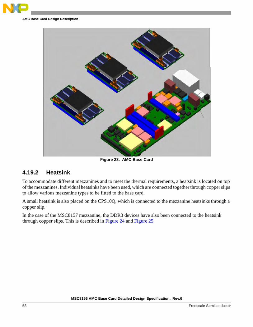
MSC8156 AMC Base Card Detailed Design Specification, Rev.0
58 Freescale Semiconductor
AMC Base Card Design Description
Figure 23. AMC Base Card
4.19.2 HeatsinkTo accommodate different mezzanines and to meet the thermal requirements, a heatsink is located on top of the mezzanines. Individual heatsinks have been used, which are connected together through copper slips to allow various mezzanine types to be fitted to the base card.
A small heatsink is also placed on the CPS10Q, which is connected to the mezzanine heatsinks through a copper slip.
In the case of the MSC8157 mezzanine, the DDR3 devices have also been connected to the heatsink through copper slips. This is described in Figure 24 and Figure 25.
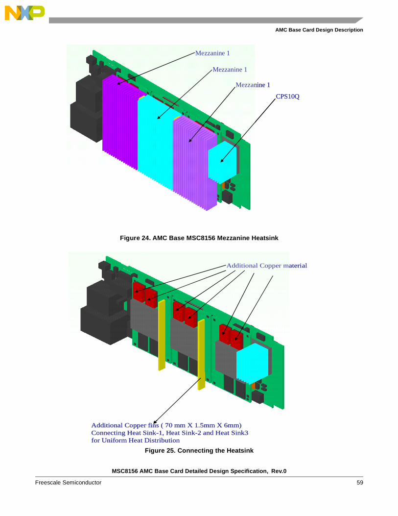
MSC8156 AMC Base Card Detailed Design Specification, Rev.0
Freescale Semiconductor 59
AMC Base Card Design Description
Figure 24. AMC Base MSC8156 Mezzanine Heatsink
Figure 25. Connecting the Heatsink
Mezzanine 1
Mezzanine 1
Mezzanine 1
CPS10Q
Mezzanine 1
Mezzanine 1
Mezzanine 1
CPS10Q
Additional Copper fins ( 70 mm X 1.5mm X 6mm) Connecting Heat Sink-1, Heat Sink-2 and Heat Sink3 for Uniform Heat Distribution
Additional Copper material
Additional Copper fins ( 70 mm X 1.5mm X 6mm) Connecting Heat Sink-1, Heat Sink-2 and Heat Sink3 for Uniform Heat Distribution
Additional Copper material
MSC8156 AMC Base Card Detailed Design Specification, Rev.0
60 Freescale Semiconductor
Revision History
5 Revision HistoryTable 28. Revision History
Revision Date Change Description
0 01/2010 Initial release.

MSC8156 AMC Base Card Detailed Design Specification, Rev.0
Freescale Semiconductor 61
Revision History
THIS PAGE INTENTIONALLY LEFT BLANK
Document Number: MSC8156AMCBCDDSRev.001/2010
Information in this document is provided solely to enable system and software
implementers to use Freescale Semiconductor products. There are no express or
implied copyright licenses granted hereunder to design or fabricate any integrated
circuits or integrated circuits based on the information in this document.
Freescale Semiconductor reserves the right to make changes without further notice to
any products herein. Freescale Semiconductor makes no warranty, representation or
guarantee regarding the suitability of its products for any particular purpose, nor does
Freescale Semiconductor assume any liability arising out of the application or use of
any product or circuit, and specifically disclaims any and all liability, including without
limitation consequential or incidental damages. “Typical” parameters which may be
provided in Freescale Semiconductor data sheets and/or specifications can and do
vary in different applications and actual performance may vary over time. All operating
parameters, including “Typicals” must be validated for each customer application by
customer’s technical experts. Freescale Semiconductor does not convey any license
under its patent rights nor the rights of others. Freescale Semiconductor products are
not designed, intended, or authorized for use as components in systems intended for
surgical implant into the body, or other applications intended to support or sustain life,
or for any other application in which the failure of the Freescale Semiconductor product
could create a situation where personal injury or death may occur. Should Buyer
purchase or use Freescale Semiconductor products for any such unintended or
unauthorized application, Buyer shall indemnify and hold Freescale Semiconductor
and its officers, employees, subsidiaries, affiliates, and distributors harmless against all
claims, costs, damages, and expenses, and reasonable attorney fees arising out of,
directly or indirectly, any claim of personal injury or death associated with such
unintended or unauthorized use, even if such claim alleges that Freescale
Semiconductor was negligent regarding the design or manufacture of the part.
How to Reach Us:
Home Page: www.freescale.com
Web Support: http://www.freescale.com/support
USA/Europe or Locations Not Listed: Freescale Semiconductor, Inc.Technical Information Center, EL5162100 East Elliot Road Tempe, Arizona 85284 1-800-521-6274 or+1-480-768-2130www.freescale.com/support
Europe, Middle East, and Africa:Freescale Halbleiter Deutschland GmbHTechnical Information CenterSchatzbogen 781829 Muenchen, Germany+44 1296 380 456 (English) +46 8 52200080 (English)+49 89 92103 559 (German)+33 1 69 35 48 48 (French) www.freescale.com/support
Japan: Freescale Semiconductor Japan Ltd. HeadquartersARCO Tower 15F1-8-1, Shimo-Meguro, Meguro-ku Tokyo 153-0064Japan 0120 191014 or+81 3 5437 [email protected]
Asia/Pacific: Freescale Semiconductor China Ltd. Exchange Building 23FNo. 118 Jianguo RoadChaoyang DistrictBeijing 100022China+86 10 5879 [email protected]
For Literature Requests Only:Freescale Semiconductor
Literature Distribution Center 1-800 441-2447 or+1-303-675-2140Fax: +1-303-675-2150LDCForFreescaleSemiconductor
@hibbertgroup.com
Freescale, the Freescale logo, and StarCore are trademarks or registered trademarks of Freescale Semiconductor, Inc. in the U.S. and other countries. All other product or service names are the property of their respective owners. The Power Architecture and Power.org word marks and the Power and Power.org logos and related marks are trademarks and service marks licensed by Power.org. RapidIO is a registered trademark of the RapidIO Trade Association.
© Freescale Semiconductor, Inc., 2010. All rights reserved.