module 11: pcb design flow, transferring a design and ... 11... · module 11: pcb design flow,...
TRANSCRIPT

Module 11: PCB Design Flow, Transferring a Design and Navigation

Module 11: PCB Design Flow, Transferring a Design and Navigation
11.1 PCB design process....................................................................... 11-1
11.2 Transferring design information to the PCB.................................... 11-3 11.2.1 Design synchronization ................................................................................11-3 11.2.2 Resolving synchronization errors .................................................................11-4 11.2.3 Exercise – Transferring the design ..............................................................11-5
11.3 Using the PCB Panel ...................................................................... 11-7 11.3.1 PCB Panel....................................................................................................11-7 11.3.2 PCB Rules and Violations ..........................................................................11-14 11.3.3 Exercise – Browsing a PCB document ......................................................11-15
11.4 Project Navigation and Cross Probing ....................................... 11-16 11.4.1 Compiling the PCB project .........................................................................11-16 11.4.2 Navigating ..................................................................................................11-16 11.4.3 Cross probing from the schematic to the PCB...........................................11-17 11.4.4 Exercise — Navigation and Cross Probing................................................11-18
Software, documentation and related materials:
Copyright © 2009 Altium Limited.
All rights reserved. You are permitted to print this document provided that (1) the use of such is for personal use only and will not be copied or posted on any network computer or broadcast in any media, and (2) no modifications of the document is made. Unauthorized duplication, in whole or part, of this document by any means, mechanical or electronic, including translation into another language, except for brief excerpts in published reviews, is prohibited without the express written permission of Altium Limited. Unauthorized duplication of this work may also be prohibited by local statute. Violators may be subject to both criminal and civil penalties, including fines and/or imprisonment. Altium, Altium Designer, Board Insight, Design Explorer, DXP, LiveDesign, NanoBoard, NanoTalk, P-CAD, SimCode, Situs, TASKING, and Topological Autorouting and their respective logos are trademarks or registered trademarks of Altium Limited or its subsidiaries. All other registered or unregistered trademarks referenced herein are the property of their respective owners and no trademark rights to the same are claimed.
Module Seq = 11
Module 11: PCB Design Flow, Transferring a Design and Navigation ii

11.1 PCB design process The PCB Design training covers how to use the PCB Editor to create a PCB from setup, through component placement, routing, design rule checking and CAM output. We first look at the overall PCB design process.
The diagram below shows an overview of the PCB design process from schematic entry through to PCB design completion.
Figure 1. Overview of the PCB Design Process
Module 11: PCB Design Flow, Transferring a Design and Navigation 11 - 1

Once the PCB design is completed and verified, the Create Manufacturing Output process is used to generate the PCB output files. This process is outlined below in . Figure 2
Figure 2. Work flow for generating PCB output files
Module 11: PCB Design Flow, Transferring a Design and Navigation 11 - 2

11.2 Transferring design information to the PCB
Rather than using an intermediate netlist file to transfer design changes from the schematic to the PCB, Altium Designer has a powerful design synchronization feature.
11.2.1 Design synchronization
Figure 3. Design synchronization flow
The core features of the synchroniser are:
• Difference engine – compares the schematic project to the PCB. The difference engine can compare the component and connective information between almost all kinds of documents. It can compare a schematic project to a PCB, one PCB to another PCB, a netlist to a PCB, a netlist to a netlist, and so on. The differences found by the difference engine are listed in the difference dialog.
• Difference dialog – lists all differences detected between the compared documents. You can then define which document should be updated to synchronize the documents. This approach allows you to make changes in both directions in a single update process, giving your bi-directional synchronization. Right-click in the dialog for direction options. This dialog is usually only seen when using the process Project » Show Differences.
Module 11: PCB Design Flow, Transferring a Design and Navigation 11 - 3

• Engineering Change Order dialog – Once the direction of update for the differences has been defined, a list of engineering change orders is generated. A report of these can be generated.
There are two approaches to performing an update:
• Select Design » Update to push all changes from schematic to PCB (or PCB to schematic). If you choose this option, you have indicated the direction to use, so you go straight to the ECO dialog.
• Select Project » Show Differences if you need selective control of the direction. You also use this option if you wish to compare any other document kinds, for example, to compare a netlist to a PCB (also referred to as loading a netlist into a PCB).
11.2.2 Resolving synchronization errors Most problems with synchronizing a design generally fall into two categories:
• Missing component footprints. This occurs when: - A footprint is missing from the component information in the schematic. - You have forgotten to add the required PCB libraries to the currently available libraries. - The footprint in the schematic does not match any PCB library component.
• Footprint pin numbers not matched to schematic pin numbers. Altium Designer supports user-definable pin-to-pad mapping, the default behavior is to expect the same number/letter on both sides. Pin-to-pad mapping is defined in the PCB Model dialog (edit the schematic symbol, select the footprint in the Model region of the dialog, and click Edit).
• Components not matching ( ). By default Altium Designer attempts to match the component on the schematic with the component on the PCB, using the Unique ID (UID). If there are any miss-matches the Failed to Match dialog will open, offering to attempt to match by designator instead. Generally it is better to resolve the UID mismatches, rather than matching by designator. To check and resolve unmatched UIDs, select Project » Component Links when the PCB is the active document.
Figure 4
Figure 4. Warning of component unique ID’s not matching.
Module 11: PCB Design Flow, Transferring a Design and Navigation 11 - 4

• To resolve errors, perform a Show Differences, then in the Differences dialog click the Explore Differences button. The Differences panel will appear – as well as information on what the problem is. This panel lists the objects in question on both the schematic and PCB. Click on an object to display it.
Note: If there are large scale net connectivity changes it can be easier to clear the netlist in the PCB editor, the synchronisation process will reload them all. You will then need to reapply the net information to any routing, to do this use the Update Free Primitives from Component Pads command (Design » Netlist). Be careful using this feature as it creates connections on connected copper, so if shorts exists then these shorts are propagated to the net naming.
Figure 5. Differences dialog and using cross probe to mask out problem areas.
11.2.3 Exercise – Transferring the design In this exercise, you will transfer the design data from the schematic into the new PCB that you have created. This means that all required footprints must be present in available libraries. Keep these points in mind:
• Footprints that are in your project PcbLib are automatically available • For components placed from an integrated library, such as the PIC Microcontroller, the
default state is to only look for the footprint in that integrated library, so it must be available during design transfer.
To transfer the design:
1. In the Libraries panel, click the button to open the Available Libraries dialog. This dialog shows all libraries that are currently available to you.
2. Confirm that the Temperature Sensor.PcbLib is listed in the Projects tab.
3. In the Installed tab, confirm that the following libraries are installed:
- Microchip Microcontroller 8-Bit PIC16.IntLib - ON Semi Power Mgt Voltage Regulator.IntLib. - IPC-7352 Chip_Resistor_N.PcbLib - IPC-7352 Chip_Capacitor_N.PcbLib
Module 11: PCB Design Flow, Transferring a Design and Navigation 11 - 5

4. The 2 default libraries must also be installed, Miscellaneous Devices.IntLib and Miscellaneous Connectors.IntLib. If these have been uninstalled, they can be found in the root of the \Altium Designer Summer 09\Library folder.
5. Select Design » Import Changes from Temperature Sensor.PrjPCB from the PCB editor menus. The ECO dialog displays, listing all the changes that must be made to the PCB so that it matches the schematic. Note that you do not need to open the schematic sheets, this is handled automatically.
6. Scroll down through the list of changes, they should include adding 19 components, 22 nets, 4 component classes, 1 net class and 3 design rules. Click on Validate Changes to check the changes are valid.
7. Click on Execute Changes to transfer the design data. Close the ECO dialog.
8. The components will be placed on the new PCB, positioned to the right of the board outline.
9. Save the board.
Note: If you did not complete the exercises in the previous modules, you can copy the following project and schematic documents (located in the Training\Backup folder) to the Temperature Sensor folder and then complete this exercise:
- Temperature Sensor.PRJPCB - Temperature Sensor.SchDoc - MCU.SchDoc - Sensor.SchDoc
Module 11: PCB Design Flow, Transferring a Design and Navigation 11 - 6

11.3 Using the PCB Panel This section investigates how to browse through a PCB design. The PCB panel is loaded by going to the panel control and clicking PCB » PCB.
11.3.1 PCB Panel The PCB panel provides a powerful method of examining the contents of the PCB workspace.
Figure 6. PCB Editor panel
Clicking on an entry in the panel will filter the workspace to highlight that object – the highlighting will depend on the settings of the options at the top of the panel. To begin with, enable all the options.
11.3.1.1 Browse mode selection list The drop down list at the top of the panel allows you to list, locate or edit the following PCB object types in the active PCB document:
• Components (and then Component Classes) • Nets (and then Net Classes) • From-Tos • Split planes • Differential pairs • Polygons • Hole sizes
When you select an object in the panel, it will be highlighted in the workspace, according to the options at the top of the panel. Each Browse function is described in the following pages.
Module 11: PCB Design Flow, Transferring a Design and Navigation 11 - 7

11.3.1.2 Browsing nets and net classes • To browse nets, select Nets from the drop-
down list in the PCB panel.
FP
• Click on All Nets in the Net Classes region of the dialog to browse all nets on the PCB. The nets are listed in the region below and they are also highlighted on the PCB.
• If the design includes Net Classes these are also listed. Net classes such as D[0..7] have been generated automatically from busses in the design.
• Click on a net name in the Nets region to choose it – all the objects that belong to that net are listed in the Net Items region. Also, the net is highlighted on the PCB.
• Click on an item in the Net Items region and note that it is highlighted on the PCB. Also note that the object that you clicked on is selected.
• Multi-select keys are supported. Hold SHIFT or CTRL as you click on entries in the list.
• Right-click in the Net Items section and note that you can control which net items are displayed.
• Double-click on a net name to open the Edit Net dialog. Here you can change the net name, add or remove nodes from the net and define the color of the connection lines for this net.
• The Nets and the Net Items region have multiple columns. Note that you can control the sorting by clicking the heading on a column.
• Type-ahead is supported. You can type on the keyboard to jump through the lists. Press Esc to abort the current type-ahead search and start another.
Module 11: PCB Design Flow, Transferring a Design and
igure 7. Browsing nets from the CB panel
Navigation 11 - 8
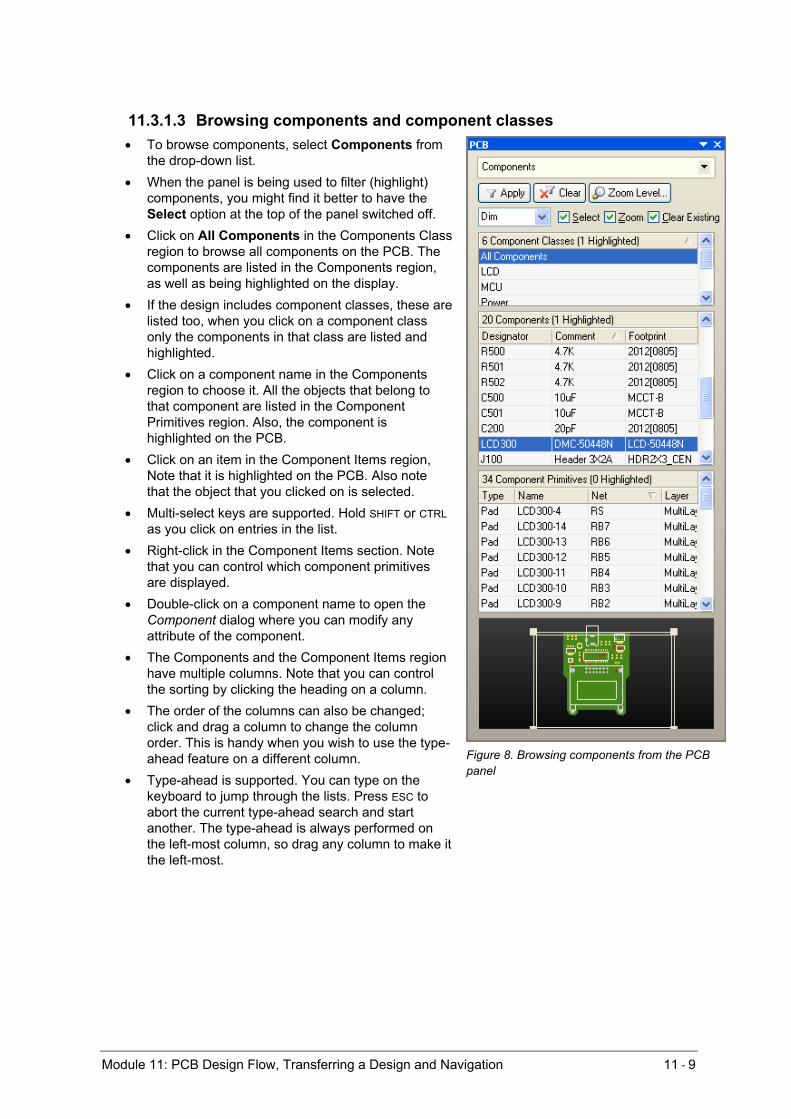
11.3.1.3 Browsing components and component classes • To browse components, select Components from
the drop-down list.
Figure 8. Browsing components from the PCB panel
• When the panel is being used to filter (highlight) components, you might find it better to have the Select option at the top of the panel switched off.
• Click on All Components in the Components Class region to browse all components on the PCB. The components are listed in the Components region, as well as being highlighted on the display.
• If the design includes component classes, these are listed too, when you click on a component class only the components in that class are listed and highlighted.
• Click on a component name in the Components region to choose it. All the objects that belong to that component are listed in the Component Primitives region. Also, the component is highlighted on the PCB.
• Click on an item in the Component Items region, Note that it is highlighted on the PCB. Also note that the object that you clicked on is selected.
• Multi-select keys are supported. Hold SHIFT or CTRL as you click on entries in the list.
• Right-click in the Component Items section. Note that you can control which component primitives are displayed.
• Double-click on a component name to open the Component dialog where you can modify any attribute of the component.
• The Components and the Component Items region have multiple columns. Note that you can control the sorting by clicking the heading on a column.
• The order of the columns can also be changed; click and drag a column to change the column order. This is handy when you wish to use the type-ahead feature on a different column.
• Type-ahead is supported. You can type on the keyboard to jump through the lists. Press ESC to abort the current type-ahead search and start another. The type-ahead is always performed on the left-most column, so drag any column to make it the left-most.
Module 11: PCB Design Flow, Transferring a Design and Navigation 11 - 9

11.3.1.4 From-To editor
Figure 9. The From-To Editor in the PCB panel
Figure 10. Use the Split Plane Editor to display and edit split planes
• Choose From-To Editor from the drop-down field at the top of the PCB panel. The top list section of the panel will fill with all nets currently defined for the design.
• As you click on a net entry, all of the nodes on that net will be loaded into the middle list section of the panel. Filtering will be applied and a mask automatically used in order to leave just the nodes (pads) on the net fully visible. All other objects are dimmed.
• Double-click on a net entry to open the Edit Net dialog where you can edit the properties of the net.
• To add a new from-to, select the Nodes on Nets to which you want to add the from-to and click the Add From To button. The new from-to appears in the From-Tos on Net section. Click on the from-to in the From-Tos on Net section and click on Generate and select a from-to topology, e.g. Shortest, Daisy varieties or Starburst.
• The From-To editor can only be used to create from-tos. To browse for existing from-tos, create a query in the Filter panel using the IsFromto keyword.
• Note that all connection lines, other than those that have been defined as From-Tos on the currently selected net, will remain dimmed. Switch the panel back to Nets to restore the display of connection lines.
11.3.1.5 Split Plane editor • You can review and edit split planes in the PCB
panel by selecting the Split Plane Editor from the drop-down list at the top of the panel.
• Select the plane you want to display by clicking on the Plane name. The split planes and their nets on that power plane are listed.
• Click on a split plane name in the Split Planes and Nets section to show the pads and vias on that split plane.
• Double-click on a split plane name to edit the net associated with the split plane.
• Right-click on a split plane name to select an option from the menu.
Module 11: PCB Design Flow, Transferring a Design and Navigation 11 - 10
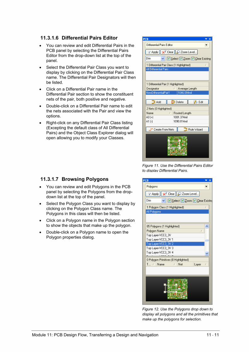
11.3.1.6 Differential Pairs Editor
Ft
• You can review and edit Differential Pairs in the PCB panel by selecting the Differential Pairs Editor from the drop-down list at the top of the panel.
• Select the Differential Pair Class you want to display by clicking on the Differential Pair Class name. The Differential Pair Designators will then be listed.
• Click on a Differential Pair name in the Differential Pair section to show the constituent nets of the pair, both positive and negative.
• Double-click on a Differential Pair name to edit the nets associated with the Pair and view the options.
• Right-click on any Differential Pair Class listing (Excepting the default class of All Differential Pairs) and the Object Class Explorer dialog will open allowing you to modify your Classes.
11.3.1.7 Browsing Polygons
Fdm
• You can review and edit Polygons in the PCB panel by selecting the Polygons from the drop-down list at the top of the panel.
• Select the Polygon Class you want to display by clicking on the Polygon Class name. The Polygons in this class will then be listed.
• Click on a Polygon name in the Polygon section to show the objects that make up the polygon.
• Double-click on a Polygon name to open the Polygon properties dialog.
Module 11: PCB Design Flow, Transferring a Design and Na
igure 11. Use the Differential Pairs Editor
o display Differential Pairs.
igure 12. Use the Polygons drop down to isplay all polygons and all the primitives that ake up the polygons for selection.
vigation 11 - 11

11.3.1.8 Hole Size Editor
Fpp
Use the Hole Size Editor mode of the PCB panel to review and manage the different drill sizes on your board. Various criteria can be defined, allowing you to locate and display only holes of interest. Criteria includes:
• Pad and/or via holes. • Plated and/or non-plated holes. • Free or component pad/via holes. • Type of hole (all, round, square or slotted
holes). • Selected and/or unselected holes. • Only the layer-pairs of interest.
Once the criteria defined, the panel lists all unique hole definitions and clusters the pads and/or vias associated with each.
• Click on a Unique Hole entry to view all of the instances of that hole size in the design, in accordance with your current highlighting options (Zoom, Mask, and Select).
• Edit the selected holes directly in the panel (ToolSize, Length, Type, Plated).
• Individual pad or via properties can be edited directly – double-click on an entry in the lower list to open the pad/via properties dialog.
Module 11: PCB Design Flow, Transferring a Design
igure 13. Use the Hole size editor to find and filter articular holes on a PCB, displaying the count and the rimitives.
and Navigation 11 - 12

Ft
11.3.1.9 3D Models Use the 3D Models mode of the PCB panel to review 3D models used in the board design.
• Click on a component to locate that component on the board and examine the 3D model.
• The panel lists each component individually, click the Footprint heading to sort by footprint kind and examine multiple components that have the same 3D model.
• Use the upper Highlighted Models dropdown to change the opacity of the currently selected 3D model.
• If the footprint includes both STEP and 3D bodies, use the check boxes to control which is currently displayed, or the lower Highlighted Models dropdown to control the opacity of one or the other types of 3D models.
• Elements that are not part of the actual board design, such as the product case, can be placed in the workspace for interference checking (Place » 3D Body). Use the *Free Models option at the top of the component list to examine and change the opacity of these elements.
Module 11: PCB Design Flow, Transferring a Design and
igure 14. Review and manage 3D models from he PCB panel.
Navigation 11 - 13

11.3.2 PCB Rules and Violations To browse design rules, Goto PCB » PCB Rules and Violations panel. All Rules classes are listed.
Figure 15. PCB Rules and Violations Panel
• Click on a Rule Class and all rules defined for that class are listed in the Rules list.
• Click on a rule in the Rules list to highlight all objects targeted by that rule.
• Double-click on the rule to display a dialog to edit that rule.
• If the selected rule is in violation, all violating objects are listed in the Violations region. To check all rules for violations, select [All Rules] in the Rule Classes section.
• Click on a violation to highlight the object causing the violation.
• Double-click on a violation to display the Violation Details dialog which details the rule that is being violated and the parameters of the primitive that is causing the violation.
• For more information about design rule checking and violations, refer to Module 12 - Design Rules.
You can also view violations by using the shortcut SHIFT + V while hovering the cursor over a violation in green.
Figure 16. The board insight for Violations
Module 11: PCB Design Flow, Transferring a Design and Navigation 11 - 14

11.3.3 Exercise – Browsing a PCB document In this exercise, you will examine the various ways to browse through a PCB document.
1. Open the document 4 Port Serial Interface.PcbDoc located in the \Altium Designer Summer 09\Examples\Reference Designs\4 Port Serial Interface folder.
2. Choose the Fit Board view command. Try the other view control options in the View menu.
3. Use the MiniViewer to move around the board.
4. Browse each object type and observe how the display changes as you click in the different sections of the panel. As you do, try the Mask, Select and Zoom options.
Module 11: PCB Design Flow, Transferring a Design and Navigation 11 - 15

11.4 Project Navigation and Cross Probing
11.4.1 Compiling the PCB project Compiling means creating a connective model (internal netlist) which converts a set of drawings into an electrically wired project. Design navigation is also enabled by compiling the design. To compile a PCB project, select Project » Compile PCB Project. (CC).
11.4.2 Navigating The DXP Navigator panel supports the traditional click-to-highlight style of browsing the design. As you click, the selected object(s) is presented on screen. You can also analyze and trace the connectivity in the design – either spatially in the actual workspace, or in the Navigator panel.
• The Navigator panel can be used to browse and cross probe to documents, components, buses, nets and pins. A single click on an entry in the panel will browse to that object in the source schematics and VHDL documents.
• Hold the Alt key as you click to simultaneously cross probe to the same object(s) on the PCB. The current document remains active, so both must be displayed for this to have any visible effect.
Figure 17. Holding down the Alt key as you click in the Navigator panel will highlight corresponding objects in both schematic and PCB documents.
• Navigation highlighting options are controlled from the System – Navigation page of the Preferences dialog (DXP » Preferences). Alternately this dialog can be accessed by clicking the … button to the right of the Interactive Navigation button.
Module 11: PCB Design Flow, Transferring a Design and Navigation 11 - 16

Figure 18. Preference dialog controlling the highlighting navigation options.
• The Connective Graph option is useful for showing the connection relationships between different components (green links) and Nets (red links).
• Pressing the Interactive Navigation button causes the component instance information to be updated in the Navigator panel when design elements are selected in the schematic sheet.
• The Navigator panel lets you view components and nets by individual sheets or hierarchical groups. Use the flattened hierarchy to see all the components and nets in your design.
11.4.3 Cross probing from the schematic to the PCB Cross Probing is a powerful searching tool to help you locate objects in other editors by selecting the object in the current editor.
• Often when you are analyzing/debugging your design you will want to cross probe from the schematic to the PCB. Full cross probing support is provided, for nets, pins and components.
• You can also cross probe all nets in a bus, and the contents of an entire sheet. • Use the Cross Probe button to be able to click on an object in one view (say the schematic)
and display the same object in another view (say the PCB). • The default behavior is to find the object in the target document then return to the source
document. Hold the CTRL key as you cross probe to jump to the target document. • You can also cross probe using the Navigator panel. Hold the ALT key as you click on
something in the panel to highlight it in both the schematic and the PCB. This can be a pin, a component, a net, bus, or a sheet. This works well if you split the view to display both the schematic and the PCB.
Module 11: PCB Design Flow, Transferring a Design and Navigation 11 - 17

Module 11: PCB Design Flow, Transferring a Design and Navigation 11 - 18
11.4.4 Exercise — Navigation and Cross Probing 1. Open the project 4 Port Serial Interface.PRJPCB, found in the \Altium
Designer Summer 09\Examples\Reference Designs\4 Port Serial Interface folder.
2. Open the schematic, ISA Bus and Address Decoding.SchDoc and the PCB document, 4 Port Serial Interface.PcbDoc. Tile these windows vertically.
3. Make ISA Bus and Address Decoding.SchDoc the active document. Use the Navigation panel to highlight components and nets in the schematic.
4. Hold down the Alt key when selecting a component or net from the Navigation panel to cross probe to the PCB.
5. Make 4 Port Serial Interface.PcbDoc the active document and click on the Cross Probe toolbar button.
6. Click on component S1. The Schematic Editor opens the related schematic document and displays the component S1 centred in the Design window.
7. Click on the Cross Probe toolbar button in the Schematic Editor and click on D1. The PCB document displays zoomed in on the component.
8. Now try cross probing nets and pads/pins between the open editors.
9. Close all open documents without saving any changes.