model 5056 - fastpulse technology, inc
TRANSCRIPT
FastPulse Technology, Inc.
LASERMETRICS ® Division 220 MIDLAND AVENUE
SADDLE BROOK, NJ 07663 TEL (973) 478-5757 FAX (973)-478-6115
Web Sites: www.lasermetrics.comwww.fastpulse.com
USERS’ GUIDE
FOR MODEL 5056SC-A-8 HIGH VOLTAGE
Q-SWITCH DRIVER MODULE
SERIAL No. ####
RoHS2 COMPLIANT
CAUTION: HEAT SINKING IS RECOMMENDED FORHIGH VOLTAGE, HIGH FREQUENCY OPERATION
WHEN CALLING OR CORRESPONDING ABOUT THIS INSTRUMENTALWAYS MENTION THE SERIAL NUMBER.
©\MANUALS\5056SC-A -ALL REV: 14 March 2016 / RLG &2018mp

1.0 INTRODUCTION
The 5056SC-A HV Q-Switch Driver Module is designed for operation with Pockels Cell Electro-Optic Q-Switches. With the appropriate Pockels cell and polarizer(s), the combination of elementsconstitute a system that can produce Q-switched laser pulses exhibiting pulse widths as short as 5nanoseconds and peak power densities of up to 850 Megawatts/cm2, depending on the laser cavityconfiguration. The 5056SC can also be utilized in optical gating applications (intensity orpolarization modulation) when the Pockels cell is located extra-cavity. The system is self-contained, requiring only a low voltage DC power input and a trigger signal to activate operation.
The 5056SC HV Q-Switch Driver Module (Module) incorporates a low voltage to high voltage DCto DC converter and the HV pulse generating output circuit. The only power supply voltagenecessary is a voltage regulated +24 Volts DC supply with a current capacity of at least 1.5amperes.
Output pulses are generated by application of a TTL level input trigger signals. Output pulsecharacteristics are independent of the trigger waveform when the trigger signals are within definedlimits. Output pulse amplitude may be adjusted by means of a miniature potentiometer accessibleon the pulse module.
HV output pulses are applied to a Pockels Cell Electro-optic Q-switch (PC) which provides theoptical polarization transitions for controlling laser cavity gain. In the cavity low gain state, thelaser material is forced to store optical energy. When rapidly switched to the high gain state, thelaser material releases stored energy in an extremely brief, high intensity optical pulse.
TRIGGER SIGNALS
Only one positive going trigger signal is needed to initiate operation, i.e., one trigger pulsegenerates one output pulse. The trigger signal voltage can have an amplitude of between +2 to +5 volts. To prevent false triggering and to maximize noise immunity, the trigger signalvoltage should be set close to 4 volts. Trigger pulse widths between 50 nsec to 1 microsec. areacceptable.
HEAT SINKING & Ground
For continuous operation at room temperature ambient and repetition rates less than 50 Hz, heatsinking the 5056SC Module is recommended but not required. For continuous, long termoperation at higher repetition rates and particularly with maximum or near maximum voltage outputpulse amplitudes, heat sinking to a thermal sink maintaining a maximum base temperature of<300C is required. A suitable thermal transfer compound must be used between the 5056SCmounting surface and the sink to maximize heat transfer. When thermal transfer compoundmaterial is used between the base and mounting surface, the junction may not provide a reliableelectrical ground connection. We recommend using a separate ground wire connected to the 5056SC. . The knurled Bindingpost is intended for use to ground the driver. If ground via main enclosure is desired a bolt passingthrough one of the mounting slots to a grounded mounting surface is possible or utilizing one of thefront or rear end plate screws. (Acetone, Ketone or nail polish remover can be used on cottonswap to remove a small area of black paint to insure proper metal connection).
Page -2-
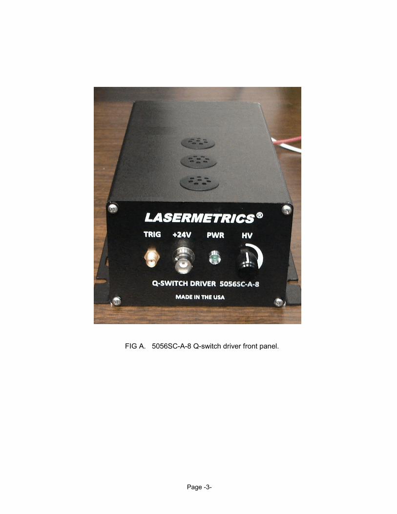
FIG A. 5056SC-A-8 Q-switch driver front panel.
Page -3-

WARNING
HIGH VOLTAGE
HV pulse amplifiers and generators contain voltages which can be dangerous or lethal ifcontacted. All reasonable safety precautions have been taken in the design and manufacture ofthis instrument. DO NOT attempt to defeat the protection provided.
This equipment should be maintained only by qualified personnel who are familiar with highvoltage components, circuits and measurement techniques. If qualified personnel are notavailable, the equipment should be returned to FastPulse for maintenance and repair.
Power must be removed and high voltage capacitors should be discharged prior to anymaintenance work. Connect and disconnect all connectors only when DC power is turnedoff.
Only recommended replacement parts should be used. We suggest that you contact thefactory before attempting to make repairs, replacements or internal adjustments. In manyinstances our engineers can provide information to help diagnose the problem and suggest anappropriate repair procedure.
HV should be turned off by removing the DC Supply voltage when the 5056 is not inactive use. Long term, static operation can effect component lifetimes when they are
subjected to continuous high voltage.
Page -4-

2.0 MODEL 5056SC-A HIGH VOLTAGE PULSE GENERATOR
Nominal Specifications and Data Sheet
SERIAL No. #### (4 Digit)
MODEL: HV PULSE OUTPUT RANGE 5056SC-A-8 ............... 1.0 to 8.0 kV @3000 Hz Max.
........Up to 6 kV @5 kHz Max.
DC VOLTAGE REQUIRED (BNC terminated) Voltage +24 VDC, +4/-0 volt Power ~28 watts, typical at max. Rep. Rate +24VDC Power Supply MW4024F (+24V, 1.6A Provided if highlighted)
TRIGGER INPUT Voltage Min. +2 volts to Max. +5.0 volts Pulse Width* Min. 50 nsec, Max. 1 μs, rise <3-5ns optimal (*Initiates HV switching unrelated to the fixed HV pulse
width to cell)
REPETITION RATE @ 8KV Single Shot to 3 kHzREPETITION RATE @ 6KV Single Shot to 5 kHz
HV OUTPUT TRANSITION TIME, 10-90% 3 ns (5-7pF load)
HV OUTPUT PULSE WIDTH Full Voltage ~2 μs
HV OUTPUT PULSE WIDTH, FWHM ~18 μs (50%)
HV OUTPUT PULSE RECOVERY TIME** ~60 μs (10-90%) **Cell returns to “OFF” state ~100us.
INPUT TRIGGER TO OUTPUT HV PROPAGATION DELAY ~50 ns
NOTES:
1. This unit provided with 15cm HV lead to cell. Long leads 20-25cm can result in large EMIfrom wires and HV reflections oscillations after pulse. For Q-switch application this is typicallynot a problem.
In applications which several S to 10's s of optical beam signal are utilized contact factory foroptions.
Page -5-

5056SC - A OPERATIONAL AND CONTROL FUNCTIONS
TRIG Trigger Input Connector: SMA Connector - Provides connection to Positiveexternal trigger source
+24 VDC BNC Connector: For connecting to an external +24 VDC power source
PWR Power Applied Lamp: Indicates +24 VDC voltage is applied to the Driver
HV Adjusts DC High Voltage and HV Output Pulse Amplitude
HV OUTPUTS - (Length 15cm, Standard termination 2mm gold pin) Red and White Wires: White wire PULSED carries the switched HV pulse (from +DCHV to ground)Red wire has fixed DCHV. DCHV on both wires is adjusted simultaneously byfront panel HV adjustment knob. Single turn Potentiometer.
FIG B: 5056SC-A-8 Outline mounting dimensions.
Page -6-
3.0 SYSTEM CONNECTION
NOTE: The 5056SC-A outputs can be connected in three different output configurations toaccommodate differing applications. Refer to Figures 1, 1a and 1b to decide whichconfiguration is suitable for the intended application.
Before proceeding with system connection, insure that the DC Power Supply (provided byuser) is turned OFF and that the VDC Control knobs (if any) are turned to zero voltage (usuallyfull counterclockwise).
3.01 Connect an appropriate trigger source to the TRIGGER input of the 5056SC-A Pulse Module(PM). Use a 50 ohm cable (RG-58/U or RG-188A) with SMA connectors. (Cable provided with driver)
3.02 Connect the +24 DC voltage supply to the +24 V BNC connector on the 5056SC front panel. The supply voltage must not exceed +28 volts DC.
3.1 INPUT FUNCTIONS
The input Trigger jack (SMA connector) will accommodate positive pulse sources. Do not exceed 5.0volts pulse amplitude or pulse widths of more than 1 μs.Do not exceed max rated kHz trigger repetition rates. (Check your driver specifications)
4.0 OPERATION
NOTE: To initially align the Pockels cell it may be necessary to employ a photodetector with a DCresponse. It is recommended that alignment be performed with a low power (<10 milliwatt He-Ne laser). Focusing optics may be needed to concentrate the beam if the detector does not have high sensitivity. The focusing optics must be removed from the system when a high power laser is used. Refer to theUser Guide For Modulators and Q-switches at the rear of this manual for additional information onalignment and cautionary practices.
After aligning the Pockels cell (PC), adjust the HV potentiometer on the PM to the maximum output level(clockwise rotation and energize the DC Power Supply (+24 VDC). This is a general starting point. Energize the laser and apply a trigger signal to the PM Trigger Input connector. This trigger must bedelayed in time from the beginning of the flash lamp pump cycle to allow the laser rod to store adequateenergy for generating a Q-switched pulse. The optimum time delay is specific to each laser and pumpenergy. Typical values range from 100 μs to 500 μs. At this time, the output beam of the laser must bemonitored by a fast rise time photodetector and the detected waveform displayed on an oscilloscope. AQ-switched pulse may be present. If not, vary the time delay between the flash lamp firing and the PMTrigger Input. If no Q-switched pulse is present, set the delay to approximately 400 μs (assuming thatthe flash lamp pulse is at least 500 μs wide) and then adjust the HV potentiometer counterclockwiseuntil a Q-switched pulse appears. To maximize the Q-switch pulse amplitude, adjust time delay and HVto achieve the desired pulse level.
The value of HV will generally be the quarter or half-wave voltage of the Pockels cell (depending on thecavity configuration and the Q-switch type used). Consult the Pockels cell data sheet for the DC testvoltage measured at 633 nanometers. The voltage required to attain any given retardation with avoltage pulse will be approximately 15% higher than the DC test voltage due to the lower AC electro-optic coefficient. Required voltage is directly proportional to wavelength and if operation at awavelength other than 633 nm is required, the Pulsed Output voltage will have to be adjustedaccordingly by increasing or decreasing the HV level.
Page -7-

MODEL 5056 Q-SWITCHING SYSTEM
5.0 GENERAL
The Model 5056SC-A (5KV and 8KV types) HV Pulse Module are designed to operate withcapacitive type Pockels cell Electro-Optic Q-switches (PC) such as the Lasermetrics Q1059, 1145,CF1042 DKDP type and 1147 RTP type , and 1150 BBO series Pockels cell EOM light modulators. The operating voltage range is preset at the factory to correspond to the type of Q-Switch being usedand the wavelength of operation. The standard 5056SC-A HV Pulse Module can be used in any ofthe 3 configurations described below.
Figure 1, MODE 1 indicates the equivalent output circuit of the 5056SC-A HV Pulse Module withbalanced output which shows that under static, unswitched conditions, the net voltage across the PC is zero. Upon triggering the unit, the voltage present on Connector 1 and thus across the PC isswitched from zero voltage to the high voltage set point.. The resulting output pulse has the formshown below the circuit. The advantage of this circuit is the absence of a net DC voltage across thePC. Continued long term application of net DC voltage may cause ion migration within the crystalresulting in fogged optical surfaces and ultimately, optical and electrical degradation of the device. The balanced output configuration provides for the zero voltage condition needed for continuous, longterm operation.
Figure 1A, MODE 2 indicates a setup of the 5056SC-A where HV is applied continuously to the PC(output not balanced). Typically this voltage is the quarter wave retardation voltage. Upon triggeringthe 5056SC-A, HV is switched to ground which permits the cavity to enter the high gain state withsubsequent build up of oscillations and generation of the Q-switched pulse. With this configuration,high voltage must not be left on unnecessarily. DC power to the 5056SC-A should be turned off whenthe unit is not in active use. In typical applications, +24 VDC is switched on and off during the operatingcycle, i.e., just prior to flash lamp firing, +24 volts is applied to the 5056SC-A. High voltage appearsacross the PC terminals. High voltage is sustained until a trigger signal is applied to the 5056SC-A. The HV output circuits then switch the voltage across the PC terminals to zero volts and a Q-switchpulse is generated. Immediately after, the +24 VDC is turned off and remains off until the next cycle. When the +24 VDC is switched on and off as described above the maximum repetition rate of the5056SC-A is about 50Hz. When the +24 VDC supply is applied constantly, between each output pulse,high voltage rises and recovers to its preset value in approximately 60 to 70 microseconds andtherefore maximum repetition rate for this type operation is about 1 kHz. The 1 kHz limitation isintended to prevent overloading the HV power supply and overheating the switching elements.
A third configuration, shown in Figure 1B, MODE 3 is common in low repetition rate lasers (~50 Hz). This arrangement uses a DC voltage blocking capacitor to prevent DC voltage from being applied to thePC. The blocking capacitor must be rated for operation at >25% higher voltage than the maximumavailable from the HV output connector. Typical values of the required capacitor are in the range of 500pf with rating 6kV to 10 kV.
Refer to “User’s Guide to KD*P & Lithium Niobate Q-switches & Modulators ....” for additionalinformation on the setup and use of these devices.
Page -8-
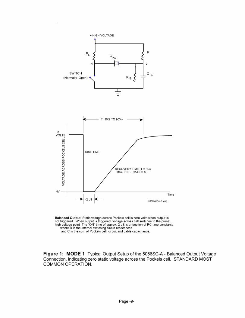
Figure 1: MODE 1 Typical Output Setup of the 5056SC-A - Balanced Output VoltageConnection, indicating zero static voltage across the Pockels cell. STANDARD MOSTCOMMON OPERATION.
Page -9-

Figure 1A: MODE 2 Single Ended Configuration - static HV is applied to Pockels cell fromConnection 1. Connection 2 is not used and must be covered by electrical tape to prevent arcing orcontact.
Page -10-

Figure 1B: MODE 3 - Using a capacitor to block HV from being applied continuously to the PC. Thecapacitor must have a voltage rating higher than the maximum voltage available from the 5056 internalHV power supply. The blocking capacitor and bleed resistor are usually connected at the PCterminals.
Page -11-
6.0 Electro-Optic Q-Switching
Intense pulses of optical radiation can be generated by Q-Switching a flash lamp or diode pumped laser with anElectro-Optic Q-Switch, also known as a Pockels Cell (PC) light modulator. The technique involves controllingthe laser beam polarization direction within the optical cavity which, in combination with a linear polarizer,introduces controllable optical losses. This prevents premature laser emission and allows energy to be stored inthe laser material through population inversion of the metastable states. When the inversion is maximized, thevoltage on the PC switches and changes the polarization conditions within the optical cavity. The availablestored energy is discharged in a single high peak power (Q-switched) pulse.
Typically, the pulse may have a duration of between 5 and 50 nanoseconds and depending on the laser material,pump energy, rod size and other interrelated parameters, the output can attain peak power densities of 50megawatts/cm2 to more than 1 Gigawatt/cm2.
Typical arrangements of laser cavity components for three common configurations for accomplishing Q-Switchingare shown in Figures 3, 4 & 5. The basic configurations are known as "quarterwave" (3 & 4) and "halfwave" (5). The terminology relates to the optical retardation produced by either the static optical elements or by the voltageapplied to the Pockels cell. , i.e., halfwave voltage is the voltage required to produce halfwave retardationbetween the o and e waves of the beam propagating through the PC crystal. Quarterwave configurations aregenerally less expensive to implement since only one polarizer is necessary. Halfwave operation is usuallypreferred when the laser rod material exhibits high gain and there is difficulty preventing premature emission. Theuse of two (2) polarizers reduces pre-lasing leakage thus improving the low Q, high loss, "Q-Spoiled" condition.
To establish the proper conditions for Q-Switching, the PC crystal must be aligned so that either its X or Ycrystallographic axis is parallel to the polarization direction of the laser (some materials such as ruby have adefined polarization axis and some rods of ruby or other materials will have Brewster angle faces which definethe polarization axis). Further, the optic axis of the PC crystal must be coaxial and parallel to the laser beamdirection to within 2 arc-minutes. The polarizer must also be accurately oriented with its polarization axis parallelto that of the laser rod. In the event that the laser material does not itself define the direction of polarization, thepolarizer is the controlling element and the PC crystal X or Y axis must be parallel to the defined direction. Inmost systems, the plane of polarization is set, for convenience, to either the horizontal or vertical direction.
Inaccuracies in alignment and orientation of these optical elements result in degraded performance,i.e., inability to Q-Switch, inability to hold off lasing action, leakage of conventional mode laser energy,low Q-Switched power, optical pulse jitter and unusual or unstable pulse shapes. These degradedperformance characteristics may exist in any combination.
CAUTION
Laser energy deflected out of the cavity through polarizerside escape surfaces can be very intense. Safety glasses or
goggles will not provide the attenuation necessary to preventeye damage. Extreme care should be taken to either diffuse,
absorb or block this energy.
Page -12-

This page is left intentionally blank for your notes or sketches.
Page -13-

Figure 3. Quarterwave Configuration: DCQuarterwave voltage is applied to prevent lasing. Voltage is then switched to zero volts to generate theQ-switched output pulse.
The quarterwave configuration illustrated in Figure 3,is the most economical, in terms of number ofcomponents used, and simplest arrangement for Q-switching with an electro-optic Q-switch. Thisconfiguration minimizes the high voltage levelrequired for efficient Q-switching. It also permitsoperation of the laser in its conventional, non-Q-switched mode by simply removing high voltage fromthe Q-switch. As explained later (Para. 7.1) certainprecautions must be observed. The configuration employs a Q-switch and a singlepolarizer. Quarterwave voltage must be appliedcontinuously to prevent lasing. The voltage isswitched to zero during the time the Q-switched pulseis to be generated.
Figure 4. Pulsed Quarterwave Configuration: DC voltage is not required to prevent lasing. Voltagepulses switching from to zero to quarterwave voltagegenerates the Q-switched optical pulse. Pulseamplitude must be (1.25) X (DC Quarterwavevoltage). The Figure 4 configuration of elementscombines the best features of the half and quarter
wave modes. This arrangement requires apolarizer and quarterwave plate in addition to theQ-switch. Use of a quarterwave plate is equivalentto applying static quarterwave voltage to the Q-switch crystal. Since voltage is applied only as abrief pulse, there is no DC voltage across thecrystal, thereby extending Q-switch life indefinitely(para. 7.1). The only disadvantage is that thevoltage pulse amplitude must be 20% to 25%higher than the static voltage used in Fig. 3. Fig. 4configuration has become the preferred mode ofoperation for many Q-switched lasermanufacturers.
Figure 5. Halfwave Configuration: DC voltage isrequired to prevent lasing. Halfwave voltage isswitched to zero to generate the Q-switched pulse
This mode requires a Q-switch and two polarizers andthus is more expensive to implement than thequarterwave mode. Another disadvantage is that avoltage pulse equal to the halfwave voltage (twice theamplitude of the quarterwave voltage) must beswitched to zero volts to generate the Q-switchedpulse. The major advantage of using two polarizers isevident in high-gain cavities where the secondpolarizer provides improved hold-off of conventionallasing.
COMPONENT DESCRIPTIONS
M1 = 100% Reflective MirrorM2 = Output Mirror (partially reflective) EOQS or PC= Electro-Optic Q-Switch λ/4 = Quarterwave PlatePolarizer = Glan-Air Spaced Calcite Polarizer, thin film or Brewster angle Polarizer
Page -14-
7.0 Q-SWITCHING PRECAUTIONS
Lithium Niobate crystals exhibit a strongpiezoelectric effect (KD*P to a lesser extent) thatcan have an adverse effect when Q-switching. The effect can be neutralized by appropriatetiming of the electrical pulse to the Q-switch.
The piezoelectric effect becomes apparent when acrystal such as lithium niobate is excited by a fastrise time electrical pulse. Physically, the crystal isexcited into mechanical oscillation--a contractionand extension effecting the indices of refraction. Inthe case of quarterwave switching, DC highvoltage is applied to the crystal to prevent lasing;the voltage is then switched to zero volts to allowthe Q-switched optical pulse to be generated. Thepiezoelectric effect, in the form of a dampedoscillation or ringing, appears some time after thevoltage is switched to zero level. The actual timeat which the ringing occurs and the frequency ofthe ringing is dependent on the physicaldimensions of the crystal. The larger the crystal,the lower the frequency and the longer the timeperiod before ringing occurs.
For instance, the typical ringing frequency of thecrystal used in the Model 3905 Q-switch isapproximately 350 kHz and the ringing mayappear about 700 nanoseconds after the voltagepulse reaches the zero volt level.
The effect of piezoelectric ringing on the laseroutput may be the generation of multiple Q-switched pulses. If the stored energy remaining inthe rod (after generation of the first Q-switchpulse) is insufficient to form additional Q-switchedpulses, leakage of laser energy in the form of alower amplitude conventional mode pulse mayoccur.
The problem can be overcome by timing theleading edge of the electrical pulse which initiatesQ-switching to occur after the peak of theflashlamp pump pulse. This can beexperimentally confirmed by monitoring theelectrical pulse to the flashlamp or the lamp lightenergy.
By varying the time delay between the start of theflashlamp pulse and the leading edge of the Q-switch driving voltage, the Q-switching action canbe made to occur at a time when the flashlampenergy has decreased to a level that will notsupport additional lasing and thus, no additionaloptical pulses will be generated until the nextflashlamp pump cycle. Usually, the timing can bechosen such that there is minimal or no decreasein Q-switched pulse amplitude. If the decayingflashlamp pulse has too much amplitude for toolong a time after the peak, then secondary pulseswill probably occur. The only solution to thischaracteristic is to shorten the trailing edge of theflashlamp pulse, make its decay time more rapid,or increase the time delay between flashlampfiring and generation of the Q-switched pulse.
7.1 OPERATION WITH DC VOLTAGE
Application of DC voltage to some Pockels cell Q-switches and light modulators for long periods oftime may result in permanent damage to theelectro-optic crystal(s).
Devices fabricated from KDP, KD*P, ADP andAD*P, in the presence of continuous (DC) highelectric fields, are subject to an ion migrationeffect. With long term application of high voltage,the polished optical surfaces become fogged andetched. All crystal surfaces, including thoseunder the conductive electrodes can be similarlyeffected. This may result in discontinuitiesbetween the crystal and electrode conductors. Application of AC electric fields, even those with anet DC value, appear to minimize the effect andextend lifetimes dramatically.
The effect is independent of the electrodematerials used and has been documented forgold, indium, silver and transparent conductiveoxide electrode materials. One manufacturerreports that a sustained voltage of 50 volts willeventually have an effect on the crystal. Use ofinert index matching fluids does not mitigate thedamage. The effect appears with or without theuse of fluid.
We recommend that DC voltage not be applied toa Pockels cell when the laser system in which it isemployed is not actively in use. When thesystem is in a standby condition, care must betaken to turn off the DC voltage to the Pockelscell. When this procedure is followed, operationallifetime of more than 5 years is not unusual andwhere this "voltage off" safeguard has beenobserved, many Lasermetrics Q-switches havebeen in active use for more than 20 years.
*From “User’s Guide For KD*P & LithiumNiobate Q-Switches and Modulators, For Q-switching, Chopping & Pulse Extraction”.
Page -15-

FastPulse Technology, Inc. LASERMETRICS ® Division 220 MIDLAND AVENUE
SADDLE BROOK, NEW JERSEY 07663 TEL (973) 478-5757
FAX (973)-478-6115 WARRANTY
Each standard component and instrument manufactured by FastPulse Technology and/or its LASERMETRICS ® Division isguaranteed to be free from defects in material and workmanship for a period of one (1) year from the date of shipmentto the original purchaser. This warranty does not apply to non-standard equipment or equipment modified to meetcustomer special requirements. The warranty period for non-standard or modified equipment shall not exceed 90days after date of invoice. All warranties are voided if such equipment is operated beyond its safe operation limits,without proper routine maintenance, or under unclean conditions so as to cause optical or other damage; or if it isotherwise abused, connected incorrectly electrically, exposed to power line or other electrical surges, or modified inany way.
Our liability under this warranty is restricted to, at FastPulse Technology's option, replacing, servicing or adjusting anyinstrument returned to the factory for that purpose, and to replacing any defective parts. Specifically excluded fromany warranty liability are indicator lamps; vacuum, gas and vapor tubes; fuses, batteries, optical coatings, componentsin lasers and laser systems such as: focusing lenses and other optical components internal or external to the lasercavity, expendable items such as flash lamps, water filters and the like. FastPulse Technology does not assumeliability for installation, patent violation claims, labor, injuries, or consequential damages.
Equipment under warranty must be returned to the factory with transportation charges prepaid and with advancenotice to FastPulse Technology. Contact FastPulse Technology’s Sales Department for a Return MaterialAuthorization (RMA). Equipment repaired under terms of this warranty will be returned to the purchaser with shippingcharges prepaid. If it is deemed impractical to return the equipment to the factory, the purchaser may request thedispatch of a FastPulse Technology service engineer whose services, transportation, and living expenses will be billedat the then current rate.
In many instances, equipment problems can, with the purchaser’s assistance, be resolved through briefcommunications with a factory engineer either by telephone, FAX or e-mail. Should, in FastPulse Technology'sopinion, the problem be caused by a component or subassembly failure, the Company shall at its discretion ship areplacement to the user, and/or request that the failed component or subassembly be returned to the factory foranalysis or repair.
This warranty does not imply and is expressly in lieu of all other liabilities, obligations, or warranties. FastPulseTechnology neither assumes nor authorizes any other person or organization to assume on behalf of FastPulseTechnology any other liability in connection with these products. FastPulse Technology disclaims the impliedwarranties of merchantability and fitness of such products for a particular purpose. It is the purchaser’s responsibilityto insure that the products are suitable for the purchaser’s application.
CLAIM FOR DAMAGE IN SHIPMENTThe equipment should be tested as soon as possible after receipt. If it fails to operate properly, or is damaged in anyway, a claim should be filed with the carrier. A full report of the damage should be obtained by the claim agent andthis report should be forwarded to FastPulse Technology. We will then advise the disposition to be made of theequipment and arrange for repair or replacement.
Include model number and serial number when referring to this equipment for any reason.
REV. 1 June 2011 /RLGC:\WP\FTI\WARRANTY
Page -16-