mn63y1210a evaluation board circuit diagram and implementation · 2 2013/10/21 connection diagram...
TRANSCRIPT

2013/10/21
Evaluation board circuit diagram and implementation< MN63Y1210A >
Evaluation board circuit diagram Evaluation board circuit diagram and implementationand implementation< < MN63Y1210AMN63Y1210A >>
Ver 1.1
2013/10/21
Automotive & Industrial Systems CompanyPanasonic Corporation

22013/10/21
Connection diagram of the evaluation boardWhen I perform 5V/3V change with a main board of the Host side, it supports UART 5V/3V change.
9
10
11
12
13
14
15
16
8
7
6
5
4
3
2
1
RX
TEST
NCLP
TX3V
TX5V
IRQ3V
IRQ5V
SEL
VDD1
NC
VA
VSS
VDD
VDD2
VB
NC
LSI-Chip
NFC-TAG-MN63Y1210A
SSOP016
1
2
3
4
5
6
7
8
Con
nect
or C2
C3C4
TC0
TC1
TP3
TP4
R0
R1
TP0 TP1
TP2
mF0.1C2
Condenser implementation for resonance frequency adjustmentpF330C6
It is for reference board alone evaluationskΩ100R0、R1
Ω0R2
mF
mF
pF
Unit
0.1C4
0.01C3
Condenser implementation for resonance frequency adjustment
Note
27
Value
C1
Element nameS8B-PH-SM4-TB
C1C6
R2selecting
switch
(SW1)CL-SB-22B-01
SW1
32013/10/21
CLK
synchronous
UART -----Unconnected PinR3
1.6x0.80.1W-0~50mΩKOARK73Z1JTTD
CLK
synchronous
UART
-----Unconnected Pin
-----Unconnected PinTP4
-----Unconnected PinTP3
-----Unconnected PinTP2
-----Unconnected PinTP1
-----Unconnected PinTP0
19.9x8.6100V--JSTS8B-PH-SM4-TBCN1
6.4x54.6V--PanasonicNFC-TAG-MN63Y1210AIC1
50V
25V
25V
25V
-
-
0.1W
0.1W
0.1W
RatedV/ W
±5%
±10%
±10%
±10%
-
-
-
±5%
±5%
Tolerance
1.6x0.8
1.6x0.8
1.6x0.8
1.6x0.8
-
-
1.6x0.8
1.6x0.8
1.6x0.8
LxW[mm]
Murata
Murata
Murata
Murata
-
-
KOA
KOA
KOA
Manufacturer
--C0
330pFGRM1885C1H331JA01D C6
0.1μFGRM188R71E104KA01D C4
0.01μFGRM188R71H103KA01D C3
0.1μFGRM188R71E104KA01D C2
--C1
0~50mΩRK73Z1JTTDR2
100kΩRK73B1JTTD104J R1
100kΩRK73B1JTTD104J R0
ParameterPart NumberNo
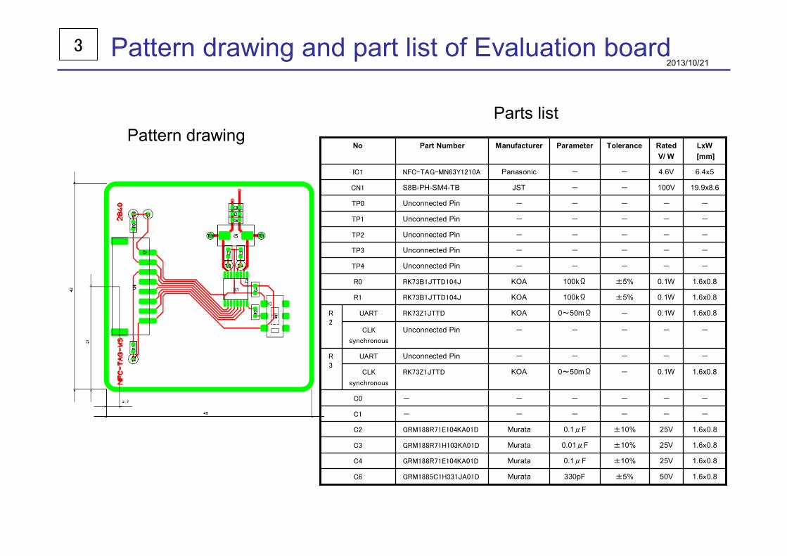
Pattern drawing and part list of Evaluation board
Parts listPattern drawing
42013/10/21
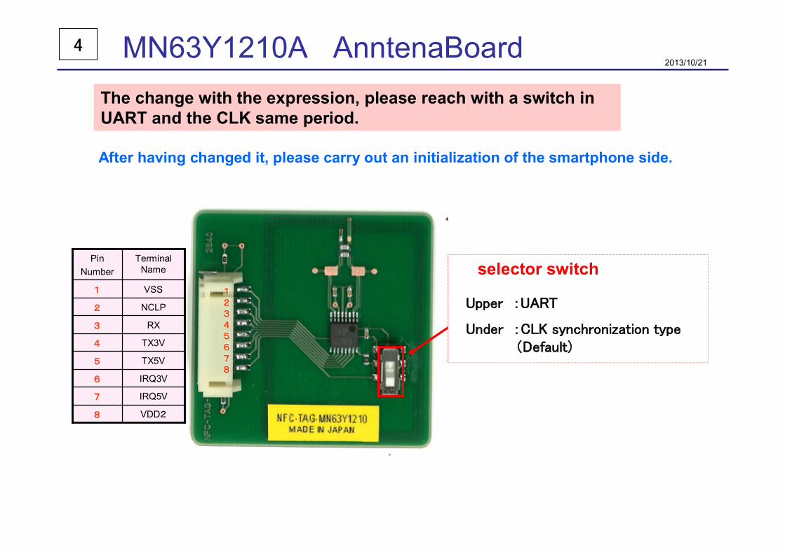
MN63Y1210A AnntenaBoardThe change with the expression, please reach with a switch in UART and the CLK same period.
After having changed it, please carry out an initialization of the smartphone side.
VSS1
VDD28
IRQ5V7
IRQ3V6
TX5V5
TX3V4
RX3
NCLP2
Terminal Name
PinNumber
12345678
12345678
selector switch
Upper :UART
Under :CLK synchronization type(Default)

52013/10/21
micro
controller
NFC-TAG-WS : UART,Serial
NFC
-TAG
-WS
Antenna
TAG circuit
Control Board Antenna Board Smartphone
RF
Connection example with MCU board for 3.3V
AntennaTAG circuit
Control BoardC
apacitor for pow
er supply stabilization
1
2
3
456
7
8
C4
C1C2
C3
C6
R0 910111213141516
87654321
RX
TESTNCLP
TX3VTX5V
IRQ3VIRQ5V
SEL
VDD1
NCVA
VSSVDDVDD2VB
NC
Capacitor for
resonance adjustm
ent
Mode
settingR
esistor
Sample antenna board circuit
Antenna Board
IRQ
UART:TXSerial:CLK
GPIO
microcontroller
UART:RXSerial:IO
R4R3Host IFUARTSerial
IF OPTION
unmounted
unmounted
mounted
mounted
R1
Serial
Outline connection diagram
3.3kΩ
3.3kΩ
MN
63Y1210A
R2

62013/10/21
micro
controller
NFC-TAG-WS : UART,Serial
NFC
-TAG
-WS
Antenna
TAG circuit
Control Board Antenna Board Smartphone
RF
Connection example with MCU board for 5V
Control Board Antenna Board
AntennaTAG circuit
Capacitor for
power supply
stabilization
MN
63Y1210A
1
2
3
456
7
8
C4
C2
C3
R0 910111213141516
87654321
RX
TESTNCLP
TX3VTX5V
IRQ3VIRQ5V
SEL
VDD1
NCVA
VSSVDDVDD2VB
NC
Capacitor for
resonance adjustm
ent
Mode
settingR
esistor
Sample antenna board circuit
IRQ
UART:TXSerial:CLK
GPIO
microcontroller
UART:RXSerial:IO
R4R3Host IFUARTSerial
IF OPTION
unmounted
unmounted
mounted
mounted
R1
Serial
3.3kΩ
3.3kΩ
5.1kΩ
C1C6Outline connection diagram
R2

72013/10/21
MCU Board[BTPB-101B]
1 VSS
2 NCLP
3 RX
4 TX3V
5 TX5V
6 IRQ3V
7 IRQ5V
8 VDD2
Antenna Board [NFC-TAG-MN63Y1210]
S8B-PH-SM4-TB(LF)(SN)(J.S.T. MFG )
Micon Board [BTPB101-B]PHR-8
(J.S.T. MFG.)
DF11-8DS-2C(HIROSE Electric)
VSS 1
RX 3
TX5V 5
IRQ5V 7
2 NCLP
4 TX3V
6 IRQ3V
8 GPIO
DF11CZ-8DP-2V(27)( Hirose Electric )
Connector specifications
Mark: 6321A

Request for your special attention and precautionsin using the technical information and semiconductors described in this book
(1) If any of the products or technical information described in this book is to be exported or provided to non-residents, thelaws and regulations of the exporting country, especially, those with regard to security export control, must be observed.
(2) The technical information described in this book is intended only to show the main characteristics and application circuitexamples of the products. No license is granted in and to any intellectual property right or other right owned byPanasonic Corporation or any other company. Therefore, no responsibility is assumed by our company as to theinfringement upon any such right owned by any other company which may arise as a result of the use of technicalinformation de-scribed in this book.
(3) The products described in this book are intended to be used for general applications (such as office equipment,communications equipment, measuring instruments and household appliances), or for specific applications as expresslystated in this book.Please consult with our sales staff in advance for information on the following applications, moreover please exchangedocuments separately on terms of use etc.: Special applications (such as for in-vehicle equipment, airplanes, aerospace,automotive equipment, traffic signaling equipment, combustion equipment, medical equipment and safety devices) inwhich exceptional quality and reliability are required, or if the failure or malfunction of the products may directlyjeopardize life or harm the human body.Unless exchanging documents on terms of use etc. in advance, it is to be understood that our company shall not be heldresponsible for any damage incurred as a result of or in connection with your using the products described in this bookfor any special application.
(4) The products and product specifications described in this book are subject to change without notice for modificationand/or improvement. At the final stage of your design, purchasing, or use of the products, therefore, ask for the most up-to-date Product Standards in advance to make sure that the latest specifications satisfy your requirements.
(5) When designing your equipment, comply with the range of absolute maximum rating and the guaranteed operatingconditions (operating power supply voltage and operating environment etc.). Especially, please be careful not to exceedthe range of absolute maximum rating on the transient state, such as power-on, power-off and mode-switching. Other-wise, we will not be liable for any defect which may arise later in your equipment.Even when the products are used within the guaranteed values, take into the consideration of incidence of break downand failure mode, possible to occur to semiconductor products. Measures on the systems such as redundant design,arresting the spread of fire or preventing glitch are recommended in order to prevent physical injury, fire, social damages,for example, by using the products.
(6) Comply with the instructions for use in order to prevent breakdown and characteristics change due to external factors(ESD, EOS, thermal stress and mechanical stress) at the time of handling, mounting or at customer's process. We donot guarantee quality for disassembled products or the product re-mounted after removing from the mounting board.When using products for which damp-proof packing is required, satisfy the conditions, such as shelf life and the elapsedtime since first opening the packages.
(7) When reselling products described in this book to other companies without our permission and receiving any claim ofrequest from the resale destination, please understand that customers will bear the burden.
(8) This book may be not reprinted or reproduced whether wholly or partially, without the prior written permission of ourcompany.
No.010618