mission peak reference server system for ngsff ssd · a detailed design overview of each component...
TRANSCRIPT
1
Mission Peak Reference Server System for NGSFF SSD
Design Guidelines for NGSFF Server Development
White Paper

2
Executive Summary NGSFF is the state-of-the-art next generation SSD form factor invented by Samsung to meet requirements of data centers and enterprise servers.
To develop a server system based on NGSFF SSD, server vendors are required to spend a significant amount of time to design thermal simulation
and Si simulation. Server vendors also have to collaborate with socket vendors to develop an appropriate socket for their designed system.
To show the superior features of NGSFF SSD for server systems, Samsung already designed and developed a NGSFF server system, called Mission
Peak, and has provided a number of public and private demonstrations. Even though this Mission Peak server system was designed as a reference
system, due to its excellent design, the Mission Peak design can be used for commercial level server production today. To help server system
vendors who want to quickly develop NGSFF server systems as their commercial product, Samsung has published this white paper explaining the
Mission Peak NGSFF reference server system.
This document describes Mission Peak architecture, designs of each component in detail, thermal simulation and measurement in a real Mission
Peak server system, as well as signal integrity simulation in order to help server system vendors to build NGSFF server system in a more time-
efficient manner.
Mission Peak Reference Server System for NGSFF SSD
1. Next Generation Small Form Factor (NGSFF) for SSD: This new form factor includes many features for enterprise server and data center server systems. Double/quadruple the Capacity of M.2, supporting multiple interfaces (PCIe, SAS/SATA, Gen-Z), High Availability through PCIe dual port supporting, Hot-insertion/removal, 12V power direct support, power-disabling capability for software reset of SSD, etc. NGSFF is under standardizationinJEDEC,anditstechnicalspecificationwasapprovedbythetechnicalcommitteein'18June.ForthedetailandadvantagesofNGSFF,pleaserefertothewhitepaperonNGSFFSSD.
Introduction of the Mission Peak (NGSFF SSD 1U Reference Server) ProjectThe Mission Peak NGSFF reference server system was designed to
achieve the higher density and higher performance in a 1U server
system by leveraging the new features and advantages of NGSFF 1.
Figure 1 shows the top level design of Mission Peak server system.
Figure 1: Mission Peak Reference System in 1U Size
7 X 40 X 56mm dual rotor hot swap fan modules
AC 1200W or 1600W 1+1 redundant high-efficiency power supply 80+
[Top view]
24 DIMM slots across 12 memory channels
2 X NIC Cards
2 X OCP Mezzanine Cards v2.0
36 X NGSFF hot swap drive bays
2 X USB 3.0
[Rear view]
[Front view]

3
Architecture of Mission Peak NGSFF Server
Table 1: Mission Peak Reference System
Feature Description / Comments
Form Factor Standard EIA-310 1U Rack mount Chassis, less than 800mm deep
SSDs Drive Bays Supporting 36 NGSFF NVMe front-loaded, hot swappable SSD bays
Boot Drive On motherboard M.2
System Firmware BIOS and BMC Features: ACPI, PXE boot, Wake-on-LAN, AC loss recovery, IPMI 2.0 KCS interface, SMBIOS, Serial console redirection, BIOS Boot Specification, BIOS Recovery Mode, SRIOV, iSCSI, TPM support, PCIe NTB
Front Panel 4 Indicator LEDs: Power Status, SSD activity, network activity, fault Others: Power on/off, 2 x USB 2.0 ports
Motherboard Key Features
Processors: 2x Intel® Xeon® Processors E5-2600 v5 (Skylake) QPI Speeds: 9.6 GT/s, 8 GT/s, 7.2 GT/sChipset: Intel® C620 Chipset System Memory: 24 DIMM slots (2 CPU sockets × 6 channels/CPU socket × two slots/channel)(DDR4 2400 (2DPC) / 2666(1DPC) MHz)LAN • For CPU0, 1 x 100GbE (PCIE add on card) + 1 x 50GbE single port (OCP) • For CPU1, 1 x 100GbE (OCP) + 1 x 50GbE dual port (PCIE add on card)
Table 1 shows the overall features of the Mission Peak NGSFF reference system:
Figure 2: Mission Peak Data-path Architecture
1U System
Intel Xeon CPU (Sky Lake)
PLX PCIe Switch
50Gb OCPNIC Mezz
100Gb PCle Card
X16
X24
18 X 4
18 x NGSFF SSD
X8
Intel Xeon CPU (Sky Lake)
PLX PCIe Switch
100Gb OCPNIC Mezz
50Gb PCle Card
X8
X24
18 x NGSFF SSD
18 X 4
X16
Architecture Overview Mission Peak is a rack mounted all-flash based storage server in a 1U EIA-310D (19”) based on NGSFF SSDs. As shown in Figure 1, Mission Peak
is comprised of 36x NGSFF SSD drives connected to a motherboard via a PLX PCIe switch fabric, dual Intel Xeon processors and 2x100Gbe and
2x50Gbe NIC cards.
The Mission Peak platform CPU is using Intel Skylake, which offers 48x PCIe Gen3 lanes. For balancing between internal SSD performance and out-
of-the-box performance through Network Interface Card (NIC), 24x PCIe lanes of each CPU are allocated to PCIe switch for NGSFF connections, and
the remaining 24x PCIe lanes are allocated to PCIe Ethernet cards. So, all the bandwidth generated between the CPU and NGSFF SSDs can be fully
delivered out of the server through the NIC. To avoid cross traffic between CPUs, which can degrade overall performance, the Mission Peak system
is designed in symmetric architecture as shown in Figure 2.

4
Architecture of Mission Peak NGSFF Server
Figure 3 shows the top-level server system design of Mission Peak.
The Mission Peak system contains the following components and features:
1) Dual Skylake Xeon E5-based Mission Peak Motherboard: It offers two Skylake CPUs, 24 DDR4 DIMMs, two PCIe x16 lanes slots and two OCP
PCIe slots.
2) PCIe Switch Mid-plane: It contains two PLX9797 PCIe switches to expand 24 PCIe lanes to 18 x 4 PCIe lanes in order to support 18 NGSFF
SSDs for each CPU
3) Orthogonal Connector: It allows the NGSFF SSD to be inserted directly into the connector without backplane, while provide enough air
channel for cooling.
4) Two PSUs: Each PSU can support up to 1600W.
5) Four Ethernet cards: System support 2x 100Gbe Ethernet cards and 2x 50Gbe OCP Ethernet cards.
Figure 4 shows the layout design for Mission Peak including the above components.
A detailed design overview of each component is provided in the following sections.
Figure 3: Mission Peak Server System Top-Level Design Figure 4: Mission Peak System Board Layout Design
CPU0
PSU1
PCH
CPU1
PSU2
50Gbe OCP
Module
100Gbe NIC Card Riser
Riser
36 x NGSFF SSD
X24 X24
X48 X48
X8 X16
X16 X8
Superslot
Superslot
100Gbe OCP
Module
50Gbe NIC Card
Switch 1 Switch 2
Back plane
NGS
FF S
SD
NGS
FF S
SD
NGS
FF S
SD
NGS
FF S
SD
NGS
FF S
SD
NGS
FF S
SD
NGS
FF S
SD
NGS
FF S
SD
NGS
FF S
SD
NGS
FF S
SD
2X100Gbe&2X50Gbe Ethernet Cards
Risers
CPUs
Redundancy PSU
DIMMs
6+1 Dual Rotor Fans
Orthogonal Connectors
PCle Switch
36 X NGSFF SSDs
Motherboard
System Fans
Mid-Plane
Drive Bay Area
5
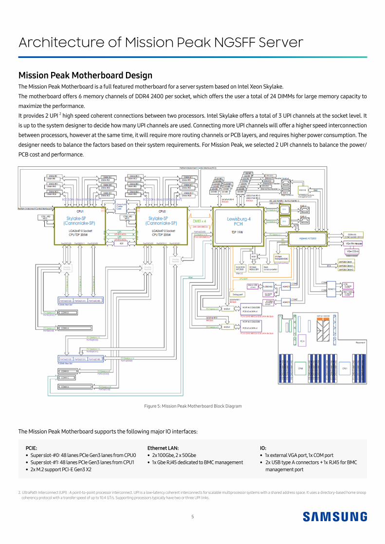
Mission Peak Motherboard Design The Mission Peak Motherboard is a full featured motherboard for a server system based on Intel Xeon Skylake.
The motherboard offers 6 memory channels of DDR4 2400 per socket, which offers the user a total of 24 DIMMs for large memory capacity to
maximize the performance.
It provides 2 UPI 2 high speed coherent connections between two processors. Intel Skylake offers a total of 3 UPI channels at the socket level. It
is up to the system designer to decide how many UPI channels are used. Connecting more UPI channels will offer a higher speed interconnection
between processors, however at the same time, it will require more routing channels or PCB layers, and requires higher power consumption. The
designer needs to balance the factors based on their system requirements. For Mission Peak, we selected 2 UPI channels to balance the power/
PCB cost and performance.
2. UltraPath Interconnect (UPI) : A point-to-point processor interconnect. UPI is a low-latency coherent interconnects for scalable multiprocessor systems with a shared address space. It uses a directory-based home snoop coherency protocol with a transfer speed of up to 10.4 GT/s. Supporting processors typically have two or three UPI links.
Figure 5: Mission Peak Motherboard Block Diagram
The Mission Peak Motherboard supports the following major IO interfaces:
PCIE: • Super slot-#0: 48 lanes PCIe Gen3 lanes from CPU0• Super slot-#1: 48 lanes PCIe Gen3 lanes from CPU1• 2x M.2 support PCI-E Gen3 X2
Ethernet LAN: • 2x 100Gbe, 2 x 50Gbe • 1x Gbe RJ45 dedicated to BMC management
IO: • 1x external VGA port, 1x COM port• 2x USB type A connectors + 1x RJ45 for BMC management port
Architecture of Mission Peak NGSFF Server

6
Architecture of Mission Peak NGSFF Server
PCIe Lane DistributionThere are 2 PCIe super slots to which each CPU connects all its PCIe lanes (i.e. 48 PCIe Gen3 lanes are connected to a superslot). To maximize the
performance of the NGSFF SSD in 1U system, all 48 PCIe lanes in the SkyLake CPU are fully used for the Mission Peak system design.
To avoid the bottleneck of the bandwidth, PCIe topology is designed in balanced and symmetric topolgy (i.e. out of 48 PCIe lanes per CPU, 24
PCIe lanes go to NIC and 24 PCIe lanes are used to connect to NGSFF SSDs). As a result, the bandwidth between SSDs to/from CPU and CPU to/
from NIC are balanced to prevent bottlenecking. And the connection between two CPUs are designed symmetrically to minimize the data traffic
between CPUs, which could be raised due to asymetricity.
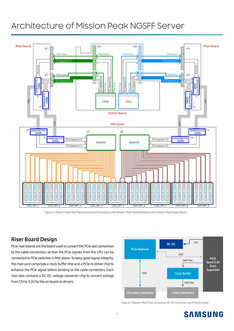
Mid-Plane DesignMission Peak Mid-plane is the system board located between the Motherboard and the NGSFF SSDs. As shown in Figure 6, it contains two PCIe
switch PEX9797. Each PCIe switch expands PCIe 24x lanes to 18 PCIe x4 lanes to support 18 NGSFF SSDs. Therefore, a total 36 NGSFF SSDs are
supported in 1U size Mission Park reference system. Midplane also includes 9 Orthorgonal connectors, which is supporting 4 NGSFF SSD each,
to support a total of 36 NGSFF SSDs. The NGSFF SSD can be directly inserted into the Orthogonal connector without additional backplane. The
Midplane contains four Slimline connectors, which can be connected with the high speed cables for 48 PCIe lanes from the Motherboard to
PEX9797 PCIe switch chip.
The Mid-plane also provides a power sequencing circuit. The Mid-plane provides the main 12V power to the NGSFF SSDs when both presence
detection pins--PRSNT 1#(Pin 67) and PRSNT 2#(Pin 6)--are detected correctly.
Super Slot # PCIe Lanes Used By Allocation For
Slot-#1
24
CPU0
Riser card and cable connect to backplane
16 100Gbe PCIe adding Card
8 50Gbe OCP Mezz Card
Slot-#2
24
CPU1
Riser card and cable connect to backplane
16 100Gbe OCP Mezz Module
8 50Gbe PCIe adding card
Table 2 – PCIe Lane Distribution (i.e Bandwidth Distribution)
7
Figure 6: Mission Peak Mid-Plane Board and Connections with Mission Peak Motherboard via the Mission Peak Raiser Board
Riser Board DesignPCIe riser boards are the board used to convert the PCIe slot connection
to the cable connection, so that the PCIe signals from the CPU can be
connected to PCIe switches in Mid-plane. To keep good signal integrity,
the riser card comprises a clock buffer chip and a PCIe re-driver chip to
enhance the PCIe signal before sending to the cable connectors. Each
riser also contains a DC-DC voltage converter chip to convert voltage
from 12V to 3.3V for the on board re-drivers.
Architecture of Mission Peak NGSFF Server
Figure 7: Mission Peak Riser Comprises DC-DC Converter and PCIe Re-driver
PCIe RedriverDC-DC
Clock Buffer
Clk Cable Connector Cable Connector
PCIE Gen3 X 24
from Superslot
X24
X24
Ref Clks
Ref Clks
12V
Riser Board
Mother Board
CPU0
PEX9797
CON_NF1_1 CON_NF1_4
Sing
le N
F1 C
ON
N
Sing
le N
F1 C
ON
N
Sing
le N
F1 C
ON
N
Sing
le N
F1 C
ON
N
Sing
le N
F1 C
ON
N
Sing
le N
F1 C
ON
N
Sing
le N
F1 C
ON
N
Sing
le N
F1 C
ON
N
Sing
le N
F1 C
ON
N
Sing
le N
F1 C
ON
N
Sing
le N
F1 C
ON
N
Sing
le N
F1 C
ON
N
Sing
le N
F1 C
ON
N
Sing
le N
F1 C
ON
N
Sing
le N
F1 C
ON
N
Sing
le N
F1 C
ON
N
Sing
le N
F1 C
ON
N
Sing
le N
F1 C
ON
N
Sing
le N
F1 C
ON
N
Sing
le N
F1 C
ON
N
Sing
le N
F1 C
ON
N
Sing
le N
F1 C
ON
N
Sing
le N
F1 C
ON
N
Sing
le N
F1 C
ON
N
Sing
le N
F1 C
ON
N
Sing
le N
F1 C
ON
N
Sing
le N
F1 C
ON
N
Sing
le N
F1 C
ON
N
Sing
le N
F1 C
ON
N
Sing
le N
F1 C
ON
N
Sing
le N
F1 C
ON
N
Sing
le N
F1 C
ON
N
Sing
le N
F1 C
ON
N
Sing
le N
F1 C
ON
N
Sing
le N
F1 C
ON
N
Sing
le N
F1 C
ON
N
CON_NF1_7CON_NF1_2 CON_NF1_5 CON_NF1_8
J2
J2
CN5
CN4
CN3
CN2
J2
J1J1
J1PCl-Express X 12
SlimLine X 12CONN
SlimLine X 12CONN
SlimLine X 12CONN
SlimLine X 12CONN
Slim
Line
X 12
CON
NSlim
Line X 12CO
NN
Slim
Line
X 12
CON
NSlim
Line X 12CO
NN
CPU0_port1 CPU1_port1CPU0_port2 CPU1_port2
PCl-E
X 8
PCl-E X 8
PCl-E X 12PCl-E
X 12
PCl-E X 4PCl-E X 4 PCl-Express X 16
PCl-E
xpre
ss X
16
PCl-E
xpre
ss X
16
PCl-E
xpre
ss X
16
PCl-E
xpre
ss X
16
PCl-Express X 16
PCl-Express X 16 PCl-Express X 16
Cabl
e
Cabl
e
Cable
Cable
PCl-Express X 12
PCl-Express X 12 PCl-Express X 12
J3
GF2GF2 PCle Clock PCle Clock
PCle Clock PCle Clock
PCle
Clo
ck
PCle
Clo
ck
PCle
Clo
ck
PCle
Clo
ck
PCle ClockPCle Clock
GF1GF1
J4
CON_NF1_3 CON_NF1_6 CON_NF1_9
U1 U5
PEX9797
CPU1
Mid-plane
Riser Board
NF1 Quad Port CONN NF1 Quad Port CONN NF1 Quad Port CONNNF1 Quad Port CONN NF1 Quad Port CONN NF1 Quad Port CONNNF1 Quad Port CONN NF1 Quad Port CONN NF1 Quad Port CONN
8
Server-side Connector Design for NGSFF SSD The connector was designed with the following goals:
1) It shall support the hot-plug feature of the NGSFF SSD form factor specification (i.e. the pins on orthogonal connector shall have two staging
pin groups; 12V pre-charge pin [Pin 36] and two presence detect signal pins--PRSNT 1# [Pin 67] and PRSNT2# [Pin 6]—are the 1st mating
group pins; Other pins are in 2nd mating group pins).
2) It shall have the role of backplane to dock the NGSFF SSD into system.
3) It shall support high density design.
4) It shall support better air flow for effective cooling compared to existing backplane design.
5) It shall provide more signal integrity margin than the existing backplane designs to support PCIe Gen3 and Gen4.
Architecture of Mission Peak NGSFF Server
Figure 9: Tray with NGSFF Loading to SystemFigure 8: NGSFF Tray Design
Tray Design for NGSFF SSD The NGSFF SSD needs to be mounted on a tray for system maintainer’s easier insertion/removal into/from the Mission Peak system.
The Mission Peak tray for NGSFF SSDs plays four major roles:
1) Physical/electrical protection of the NGSFF SSD
2) Locking the NGSFF SSD on the tray in a correct position
3) Guide the NGSFF SSD to securely plug in/out
4) Provide LED indication holes on the front panel of the tray
Figure 8 illustrates the Mission Peak NGSFF tray design and its detail features. The NGSFF Tray provides the four mounting stands for the NGSFF
SSD to be mounted on using screws. The user can use the Front Handle to lift the latch up for the NGSFF Tray to be pulled out from the server
system. LED indication holes on the front panel are designed to display the NGSFF LED light, which shows the NGSFF SSD’s status.
Figure 9 illustrates how the NGSFF SSD mounted on NGSFF Tray is inserted into the Front Bay of the Mission Peak server system.
Mission PeakNGSFF Tray
NGSFF
Mounting Stand
117 mm
LED Indication
Grid to allowAir flow in
Front HandleLift up to release latchLatch
36 mm
9
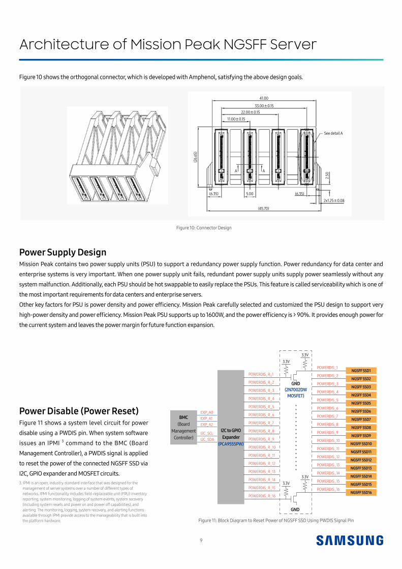
Power Supply Design Mission Peak contains two power supply units (PSU) to support a redundancy power supply function. Power redundancy for data center and
enterprise systems is very important. When one power supply unit fails, redundant power supply units supply power seamlessly without any
system malfunction. Additionally, each PSU should be hot swappable to easily replace the PSUs. This feature is called serviceability which is one of
the most important requirements for data centers and enterprise servers.
Other key factors for PSU is power density and power efficiency. Mission Peak carefully selected and customized the PSU design to support very
high-power density and power efficiency. Mission Peak PSU supports up to 1600W, and the power efficiency is > 90%. It provides enough power for
the current system and leaves the power margin for future function expansion.
Figure 10 shows the orthogonal connector, which is developed with Amphenol, satisfying the above design goals.
Power Disable (Power Reset) Figure 11 shows a system level circuit for power
disable using a PWDIS pin. When system software
issues an IPMI 3 command to the BMC (Board
Management Controller), a PWDIS signal is applied
to reset the power of the connected NGSFF SSD via
I2C, GPIO expander and MOSFET circuits.
Figure 10: Connector Design
41.00
(45.70)
A A
33.00±0.1522.00±0.15
2x1.25±0.08
11.00±0.15
(26.
65)
2.50
See detail A
(6.35) (6.35)5.00
Figure 11: Block Diagram to Reset Power of NGSFF SSD Using PWDIS Signal Pin
3. IPMI is an open, industry-standard interface that was designed for the management of server systems over a number of different types of networks.IPMIfunctionalityincludesfield-replaceableunit(FRU)inventory reporting, system monitoring, logging of system events, system recovery (including system resets and power on and power off capabilities), and alerting. The monitoring, logging, system recovery, and alerting functions available through IPMI provide access to the manageability that is built into the platform hardware.
Architecture of Mission Peak NGSFF Server
POWERDIS_R_1
POWERDIS_R_2
POWERDIS_R_3
POWERDIS_R_4
POWERDIS_R_5
POWERDIS_R_6
POWERDIS_R_7
POWERDIS_R_8
POWERDIS_R_9
POWERDIS_R_10
POWERDIS_R_11
POWERDIS_R_12
POWERDIS_R_13
POWERDIS_R_14
POWERDIS_R_15
POWERDIS_R_16
POWERDIS_1
POWERDIS_2
POWERDIS_3
POWERDIS_4
POWERDIS_5
POWERDIS_6
POWERDIS_7
POWERDIS_8
POWERDIS_9
POWERDIS_10
POWERDIS_11
POWERDIS_12
POWERDIS_13
POWERDIS_14
POWERDIS_15
POWERDIS_16
EXP_A0EXP_A1EXP_A2
I2C_SCLI2C_SDA
I2C to GPIOExpander
(PCA9555PW)
BMC(Board
ManagementController)
GND(2N7002DW
MOSFET)
NGSFF SSD1
NGSFF SSD9
NGSFF SSD5
NGSFF SSD13
NGSFF SSD3
NGSFF SSD11
NGSFF SSD7
NGSFF SSD15
NGSFF SSD2
NGSFF SSD10
NGSFF SSD6
NGSFF SSD14
NGSFF SSD4
NGSFF SSD12
NGSFF SSD8
NGSFF SSD16
GND
3.3V
3.3V
3.3V
3.3V

10
Architecture of Mission Peak NGSFF Server
Figure 12: (Example) I2C to GPIO Expander, PCA9555PW Figure 13: (Example) MOSFET, 2N7002DW to Drive the Signal
Figure 14: NGSFF SSD Connector Side Schematic
Figure 12 shows the schematic for I2C to GPIO expander using a PCA9555PW chip.
Figure 13 shows a gate implementation using a 2N7002DW MOSFET chip. Figure 14 shows a schematic of the NGSFF connector.
PWDIS_R_16PWDIS_R_17PWDIS_R_18PWDIS_R_19PWDIS_R_20PWDIS_R_21PWDIS_R_22PWDIS_R_23PWDIS_R_24PWDIS_R_25PWDIS_R_26PWDIS_R_27PWDIS_R_28PWDIS_R_29PWDIS_R_30PWDIS_R_31
45678910111314151617181920
I/O_0_0I/O_0_1I/O_0_2I/O_0_3I/O_0_4I/O_0_5I/O_0_6I/O_0_7I/O_1_0I/O_1_1I/O_1_2I/O_1_3I/O_1_4I/O_1_5I/O_1_6I/O_1_7
A0A1A2
SCLSDA
VDDVSS
INT#
2123
2223
2412
1
EXP_A0EXP_A1EXP_A2
I2C SCLI2C SDA
INT#_13
10K 1%10K 1%10K 1%10K 1%10K 1%10K 1%10K 1%10K 1%10K 1%10K 1%10K 1%10K 1%10K 1%10K 1%10K 1%10K 1%
0.1 uF10%25V
+3V3_I2C
+3V3
PCA9555PW
+3V3
PWDIS_30
PWDIS_R_30
10K1%
1
2
S1
G1
2N70D2DW
D1
GND GNDPERN3PERP3GNDPETN3PETP3GNDPETN2PETP2GNDPETN2PETP2GNDPERN1PERP1GNDPETN1PETP1GNDPERN0_SATA - B - 6MBPERP0_SATA-B-GNDPETN0_SATA-A-PETP0_SATA-A+GNDREFCLK_NREFCLK_PGND
PRSNT1# PEDET(NC-PCIE)GNDGNDGND
PCIE_RX_N_PR_X4.PCIE_RX_P_PR_X4.
PCIE_TX_N_PR_X4.PCIE_TX_P_PR_X4.
PCIE_RX_N_PR_X3.PCIE_RX_P_PR_X3.
PCIE_TX_N_PR_X3.PCIE_TX_P_PR_X3.
PCIE_RX_N_PR_X2.PCIE_RX_P_PR_X2.
PCIE_TX_N_PR_X2.PCIE_TX_P_PR_X2.
PCIE_RX_N_PR_X1.PCIE_RX_P_PR_X1.
PCIE_TX_N_PR_X1.PCIE_TX_P_PR_X1.
PCIE_CLK_A_N.PCIE_CLK_A_P.
D1D3D5D7D9D11D13D15D17D19D21D23D25D27D29D31D33D35D37D39D41D43D45D47D49D51D53D55D57
D67D69D71D73D75
NC_2NC_4
PRSNT2#_SNC_8
LED1#3.3VAUX
NC_14NC_16NC_18
GNDREFCLK_N1REFCLK_P1
GNDPWDIS
12V12V12V
12V(PRE-CHARGE)NC_38
SMB CLK(IOX0_3V3) DATA(IOX0_3V3)
ALERT#(IOX0_3V3)DUALPORTEN#
PERST1#PERST0#(1)(0_3V3)
CLKRE0#(IO)(0_3V3)PEWAKE#(IO)(0_3V3)RESERVED MFG DATA
RESERVED_MFG CLOCK
L SUSCLK(32KHZX1X0 3V3) NC_70NC_72NC_74
+3V3
PRSNT#
LED
+12V24
PWDIS
SCLSDA
ALERT#
PCIE RST ACLKREO
PCH WAKE N
SUSCLK
+3V3
10K1%
D2D4D6D8D10D12D14D16D18D20D22D24D26D28D30D32D34D36D38D40D42D44D46D48D50D52D54D56D58
D68D70D72D74
PEDET
M Key
CONN_M3_RA_Receptable_1x4
+3V3
10uF 0.1uF20%6.3V
10%25V
+12V24
22uF 0.1uF10%16V
10%25V

11
Since managing the temperature of the SSD is the most important in
a server system, a cutting plane mechanism is also used to investigate
the temperature near the NGSFF SSD in more detail. The plane is cut
in the middle of the NGSFF area, and the thermal distribution of the
cut plane is zoomed in as shown in Figure 17. The simulation results
indicate that the ambient temperature around NGSFF SSD area is kept
around 38~42°C, even though the 36 NGSFF SSDs are fully running.
This means that ambient temperature near the NGSFF SSDs is kept in
good and safe condition while running NGSFF SSDs.
Figure 15: Thermal Simulation Model Figure 16: Thermal Distribution (Simulation Results)
Figure 17: NGSFF Area Cut Plane to Thermal Analysis
Thermal & Signal Integrity (SI) Testing
Thermal Simulation Since the Mission Peak is a high-density and high-performance server, the efficient cooling capability of the server system is one of the most
important factors to be considered.
Figure 15 shows the Mission Peak thermal simulation model. It is based on the Mission Peak mechanical model plugged with all components
with their thermal characteristics. The ambient temperature is assumed as 35°C in front area. The air-flow direction is from front to rear. The air
passes through the NGSFF, Mid-plane/PCIe switch, fans, CPUs/DIMMs, PCH, high speed Ethernet cards and then heated air is pushed out of the
box through rear panel grids.
For the Ethernet Card area, because the air is already pre-heated by NGSFF SSDs, CPU, DRAMs, etc., it is more challenging to cool the entire area.
To resolve that, there are three Air Ducts added to the Ethernet Card area to guide and distribute the air effectively.
The open area ratio on the rear panel is also an important consideration. If the open ratio is too low, no matter how well the air duct is designed and
how fast the air fan runs, it can be hard for air to be moved out of the chassis to carry enough heat out the box.
Figure 16 shows the temperature distribution simulation results. The simulation results show that the temperature inside the 1U server box is
managed, distributed, and controlled very well.
Cut plane in the middle of NGSFF SSDs area
12
Thermal & Signal Integrity (SI) Testing
Measured area in Mission Peak server system
Measured Temperature (Max)
Left Side 71.1 °C
Center 67.5 °C
Right 69.6 °C
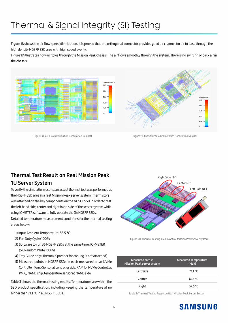
Detailed temperature measurement conditions for the thermal testing
are as below:
1) Input Ambient Temperature: 35.5 °C
2) Fan Duty Cycle: 100%
3) Software to run 36 NGSFF SSDs at the same time: IO-METER
(5K Random Write 100%)
4) Tray Guide only (Thermal Spreader for cooling is not attached)
5) Measured points in NGSFF SSDs in each measured area: NVMe
Controller, Temp Sensor at controller side, RAM for NVMe Controller,
PMIC, NAND chip, temperature sensor at NAND side.
Table 3 shows the thermal testing results. Temperatures are within the
SSD product specification, including keeping the temperature at no
higher than 71.1 °C in all NGSFF SSDs.
Thermal Test Result on Real Mission Peak 1U Server System To verify the simulation results, an actual thermal test was performed at
the NGSFF SSD area in a real Mission Peak server system. Thermistors
was attached on the key components on the NGSFF SSD in order to test
the left hand side, center and right hand side of the server system while
using IOMETER software to fully operate the 36 NGSFF SSDs.
Figure 20: Thermal Testing Area in Actual Mission Peak Server System
Right Side NF1
Center NF1
Left Side NF1
Table 3: Thermal Testing Result on Real Mission Peak Server System
Figure 18: Air-Flow distribution (Simulation Results) Figure 19: Mission Peak Air Flow Path (Simulation Result)
Figure 18 shows the air flow speed distribution. It is proved that the orthogonal connector provides good air channel for air to pass through the
high density NGSFF SSD area with high speed evenly.
Figure 19 illustrates how air flows through the Mission Peak chassis. The air flows smoothly through the system. There is no swirling or back air in
the chassis.
13
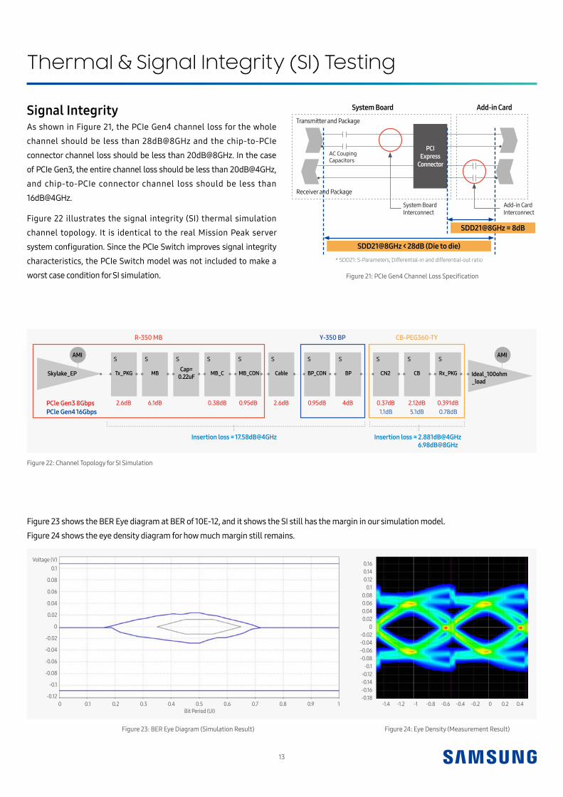
Figure 23 shows the BER Eye diagram at BER of 10E-12, and it shows the SI still has the margin in our simulation model.
Figure 24 shows the eye density diagram for how much margin still remains.
Figure 23: BER Eye Diagram (Simulation Result)
Bit Period (UI)
Voltage (V)0.1
0.04
-0.02
-0.08
0.08
0.02
-0.04
-0.1
0.06
0
-0.06
-0.120 0.40.1 0.5 0.80.2 0.6 0.90.3 0.7 1
Figure 24: Eye Density (Measurement Result)
Thermal & Signal Integrity (SI) Testing
Signal Integrity As shown in Figure 21, the PCIe Gen4 channel loss for the whole
channel should be less than 28dB@8GHz and the chip-to-PCIe
connector channel loss should be less than 20dB@8GHz. In the case
of PCIe Gen3, the entire channel loss should be less than 20dB@4GHz,
and chip-to-PCIe connector channel loss should be less than
16dB@4GHz.
Figure 22 illustrates the signal integrity (SI) thermal simulation
channel topology. It is identical to the real Mission Peak server
system configuration. Since the PCIe Switch improves signal integrity
characteristics, the PCIe Switch model was not included to make a
worst case condition for SI simulation. Figure 21: PCIe Gen4 Channel Loss Specification
Figure 22: Channel Topology for SI Simulation
S S S S S S S S S S S
Tx_PKG MB MB_CCap=0.22uF MB_CON Cable BP_CON BP CN2
0.37dB1.1dB
0.95dB2.6dB0.95dB0.38dB6.1dB2.6dBPCle Gen3 8GbpsPCle Gen4 16Gbps
Insertion loss = 17.58dB@4GHz Insertion loss = 2.881dB@4GHz 6.98dB@8GHz
4dB
R-350 MB Y-350 BP CB-PEG360-TY
2.12dB5.1dB
0.391dB0.78dB
CB Rx_PKGSkylake_EP Ideal_100ohm_load
AMI AMI
0.160.140.12
0.10.080.060.040.02
0-0.02-0.04-0.06-0.08
-0.1-0.12-0.14-0.16-0.18
-1.4 -0.6-1.2 -0.4 0.2-1 -0.2 0.4-0.8 0
* SDD21: S-Parameters, Differential-in and differential-out ratio
Transmitter and Package
Receiver and Package
SDD21@8GHz < 28dB (Die to die)
System BoardInterconnect
AC CoupingCapacitors
Add-in CardInterconnect
System Board Add-in Card
PCI Express
Connector
SDD21@8GHz = 8dB

14
Vibration and Shock Test
Figure 25: Vibration Testing Setup
Vibration Testing During OperationA vibration test was performed to verify the reliability of the system design. It vibrates the system in X, Y and Z axis, respectively, while the
system is running with the IOMETER benchmark program in order to stress CPUs, memory and NGSFF SSDs on the Mission Peak Server system.
Vibration test conditions were as follows:
1) Sinusoidal vibration -0.5G’s 0-Peak
2) 5-500-5Hz Sweep @ Octaves / minute
3) 10 sweeps
4) Bottom only tested for 3 axes
Figure 25 shows the setup of the vibration test. The operational vibration test is performed on X axis bed, Y axis bed and Z axis bed respectively.
X axis Y axis Z axis
As shown in Table 5, all vibration tests were passed. The performance measured in IOMETER is within the 10% variance during those vibration
tests.
Test Result Before Test After Test
Physical damage check Pass Pass
Functional check Pass Pass
Axis
IOMETER Test Results
Before Test(IOPS)
After Test(IOPS)
Function Test(≤10% Variance)
SSD at X axis 34,704 34,638 Pass
SSD at Y axis 34,678 33,633 Pass
SSD at Z axis 34,570 34,593 Pass
Table 4: Vibration Test Results
Operating Vibration Test

15
Vibration and Shock Test
X axis Y axis Z axis
Figure 26: Shock Testing Setup
Table 5: Shock test result
Shock Testing During OperationShock testing conditions were as follow:
1) Half sine wave shock
2) 6G (Gravity) with pulse duration of 11ms
3) 5 shocks for each of the three axes
Figure 26 shows the setup of the shock testing. The operational shock test is performed on X, Y and Z axes. The shock waveform is shown for
each axis setup. The 6G half sine shock is a particularly hard condition.
As shown in Table 5, all shock tests were passed. The performance measured in IOMETER is within the 10% variance during those shock tests.
Test Result Before Test After Test
Physical damage check Pass Pass
Functional check Pass Pass
Axis
IOMETER Test Results
Before Test(IOPS)
After Test(IOPS)
Function Test(≤10% Variance)
SSD at X axis 34,738 34,738 Pass
SSD at Y axis 34,750 34,749 Pass
SSD at Z axis 34,818 34,814 Pass
Operating Shock Test

NGSFF is the state-of-the-art SSD device form factor which is optimized for data center and enterprise server systems. To further help vendors’
NGSFF server designs, Samsung developed the Mission Peak 1U server and demonstrated its benefits through many public and private
exhibitions and demonstrations.
This white paper explains the details of the architecture and design of Mission Peak, including the Mission Peak Motherboard, PCIe lane
Distribution, Mid-plane Board, Riser Board, Tray for NGSFF SSD, Server-side Connector, Power Supply circuit and Power disabling circuit.
Reliability is also a very important consideration for servers. Thermal simulation and Signal integration simulations as well as vibration and
shock tests were performed to make sure that the Mission Peak reference design can be used for commercial product development.
If your company wants to develop NGSFF SSD based server systems, please contact us to get more detailed design information and technical
support. If you want to get the technical information on Samsung’s NGSFF SSD product, please refer to the NGSFF SSD form factor white paper or
the NGSFF SSD product brochure.
Summary
About Samsung Electronics Co., Ltd.Samsung inspires the world and shapes the future with transformative ideas and technologies. The company is redefining the worlds of TVs, smartphones, wearable devices, tablets, digital appliances, network systems, and memory, system LSI and LED solutions. For the latest news, please visit the Samsung Newsroom at news.samsung.com.
Copyright © 2018 Samsung Electronics Co., Ltd. All rights reserved. Samsung is a registered trademark of Samsung Electronics Co., Ltd. Specifications and designs are subject to change without notice. Nonmetric weights and measurements are approximate. All data were deemed correct at time of creation. Samsung is not liable for errors or omissions. All brand, product, service names and logos are trademarks and/or registered trademarks of their respective owners and are hereby recognized and acknowledged.
Fio is a registered trademark of Fio Corporation. Intel is a trademark of Intel Corporation in the U.S. and/or other countries. Linux is a registered trademark of Linus Torvalds. PCI Express and PCIe are registered trademarks of PCI-SIG. Toggle is a registered trademark of Toggle, Inc.
Samsung Electronics Co., Ltd. 129 Samsung-ro, Yeongtong-gu, Suwon-si, Gyeonggi-do 16677, Korea www.samsung.com 2018-09