microwave filters with concentrated impulse response in ...2009.telfor.rs/files/radovi/08_12.pdf ·...
TRANSCRIPT
17th Telecommunications forum TELFOR 2009 Serbia, Belgrade, November 24-26, 2009.
Abstract — This paper presents novel narrow microstrip
bandpass filter implementations with selective frequency response, suppressed time-domain sidelobes, periodically related sidelobe maxima, and minimal footprint area.
The paper is an extension of the study on the general algorithm to realize this class of filters, to form precise simulation models, to fabricate laboratory prototype, and to measure performances of the fabricated prototype.
The proposed design methodology is exemplified by a fourth-order microstrip bandpass filter, which is fabricated and measured. The simulated and measured results are in agreement in both frequency and time domain.
Key words: — impulse response, microstrip filter, miniaturization.
I. INTRODUCTION
N modern microwave receivers, for communication, radar, and satellite systems, high-performance bandpass
filters are required, which exhibit low insertion loss, high selectivity, narrow band, and optimized impulse response. Relatively narrow bandwidths are required to distinguish between pulses which are close, resulting in time-domain distortion of the pulses. If the filter design results in significant time-domain overshoots, a receiver channel will be saturated for a time considerably longer than the pulse length and hence will be unable to respond to a lower-level signal in this time period. According to the previous work on filter synthesis, it has been known that a filter based on the Rhodes prototype [1], [2], satisfies the required level of inter-channel rejection and presents a time-domain response with low sidelobe levels and periodically related zeros.
This paper focuses on microstrip realization of relatively narrow bandwidth filters with time-domain sidelobes more than dB30 below the main lobe [3]. Our objective is to
design a compact structure based on the Rhodes prototype. We consider various structures: parallel-coupled half-wavelength resonator filters, hairpin-line filters, pseudocombline filters, interdigital, and combline filters. We compare their characteristics (time-domain response, frequency response and footprint) and select the optimal structure. We explain the design methodology and show the results generated by electromagnetic (EM) simulation [4], [5], and the measurement results made on the
Milka M. Potrebić, School of Electrical Engineering, University of
Belgrade, Serbia (phone: 381-11-3370-143; fax: 381-11-324-8681; e-mail: [email protected]).
fabricated structure. Hence, conclusions are drawn about the performance of the analyzed structure.
II. DESIGN METHODOLOGY
A. Lowpass prototype
A lowpass prototype, reported in [1], has the impulse response (Figure 1) of the form
( ) ( )2εsine 1221 tKts nt
n−−= , (1)
which is the inverse Laplace transform of the corresponding scattering parameter )(21 sS , and it
represents the transfer from port 1 to port 2; t represents time normalized to s1 , n is a positive integer, and nK
and ε are real constants.
Figure 1 Impulse response of the prototype defined by
(1): 4=n , 84336.0ε = .
The corresponding transfer function for the lowpass prototype, normalized to ( ) 1021 =S , is of the form
( )
( )( )
( ) ( )( )
++
++
+
−++
=
∏
∏−
=
=
odd1ε41
14121
even1ε121
141
21
122
2
122
21
nr
sss
nr
ss
sS n
r
n
r (2)
where
211 =K , ( ) ( )ε2ε1 22 +=K ,
( )( ) ( )( )2222 ε1ε11 +++=+ nnnKK nn . (3)
Sidelobes of the impulse response are defined as shown in Figure 2. According to the terminology introduced in [1], the relative loss of the impulse response is defined as
( ) ( ) ( )( )tststA 21max2110log20= , (4)
Microwave Filters with Concentrated Impulse Response in Microstrip Technology
Milka M. Potrebić
I
883
Figure 2 Relative loss of the prototype: 4=n ,
84336.0ε = .
where )( max21 ts is the global maximum of the impulse
response which occurs at ( ) ( )( )ε1tanε2 1max −= − nt .
The attenuation of the m th sidelobe is
( ) ( )( )
( ) dBεπ686.8elog20
log20
επ
10
21max2110
m
tstsA
m
mm
==
==, (5)
where ( )mts21 is the value of the m th local extremum
which occurs at ( ) ( )( )( )ε1tanε2 1 −+π= − nmtm
( K,3,2,1=m ). Therefore, the sidelobe attenuation mA is
proportional to m and the sidelobe maxima mt are
equidistant.
The parameter ε is obtained when ( ) 221 jωS exhibits a
first-order maximally flat behavior around 0ω = . For n odd, there is no real value of ε that satisfies the first-order maximally flat behavior. However, for n even, there is always one real value of ε [1].
B. Bandpass filter
In this paper, we consider the fourth-order bandpass filter centered at GHz20 =f , with a relative bandwidth
08.0=∆B , and nominal impedances (at both ports)
Ω= 500Z .
The fourth-order transfer function (2) has the optimal value of 0.84336ε = . The attenuation of the first sidelobe (Figure 2) is dB321 =A . The corresponding filter
prototype is a minimum-phase ladder network (Figure 3a) with the normalized element values 1.49701proto1, =C ,
1.63230proto2, =L , 0.62417proto3, =C , and
0.48887proto4, =L . The prototype insertion loss is dB3 at
the normalized cutoff frequency rad/s1protop, =Ω . The
source and load resistances are equal to Ω1 .
By transforming the lowpass prototype, we obtain the bandpass filter shown in Figure 3b. The nominal impedances of both ports are 0Z . Each prototype inductor
of inductance proto,iL is replaced by a series LC resonator
with ( )0proto,0protop, ω∆Ω= BLZL ii and ( )ii LC 20ω/1= ,
where 0dB3 ω/ω∆=∆B is the normalized dB3
bandwidth, dB3dB3 2ω f∆π=∆ is the dB3 bandwidth, and
00 2ω fπ= is the center angular frequency of the bandpass
filter. Each prototype capacitor of capacitance proto,iC is
replaced by a parallel LC resonator with
( )00proto,protop, ω ZBCC ii ∆Ω= and ( )ii CL 20ω/1= .
Figure 4 shows the scattering parameters of the LC bandpass filter.
The impulse response of the LC bandpass filter, shown in Figure 5, is concentrated in the time interval ba ttt ≤≤
and practically vanishes after bt . To obtain a better insight
into this waveform, we plot the relative loss, identify the envelope of the relative loss, and determine the sidelobe attenuation (Figure 6).
proto,1C
proto,2L
proto,3C
proto,4L
1L 3C 3L
2L 2C 4C4L
1C
)b()a(
Figure 3 (a) Lowpass prototype, (b) LC bandpass filter derived from the prototype.
1.4 1.6 1.8 2 2.2 2.4 2.6-60
-50
-40
-30
-20
-10
00
f [GHz]
S11
[dB]
S21
[dB]
Figure 4 Scattering parameters of the LC bandpass filter.
Figure 5 Impulse response of the LC bandpass filter.
III. COUPLED RESONATOR FILTERS
Filters with coupled resonators can be realized as a
884

linear inductive transformer with n ports, Figure 7.
Figure 6 Relative loss of the LC bandpass filter ( dB5.321 =A , dB652 =A , ns33.4max =t ,
ns5.151 =t , ns26.672 =t ).
KK
2,1L
nL ,1 1,1 −nL
2C
2I
2L
nC
nL
nR
nI
1−nC
1−nL
1−nI
1L
+1I
1C
1R
gU
nL ,21,2 −nL
nnL ,1−
Figure 7 Filter with coupled resonators realized as a
linear inductive transformer.
On the first port, the transformer is supplied by a voltage source ( )tvg connected in series with the resistor 1R and
the capacitor 1C . At the n th port, the transformer is
terminated by a series combination of a resistor and a capacitor. All other ports of the transformer are terminated by the capacitor iC , 1,,2 −= ni K .
The impedance matrix of this coupled resonator filter can be represented as
[ ]
ω−ω−
ω−ω
+ωω−
ω−ω−
=
nnnn
n
n
ZLL
LC
LL
LLZ
,2,1,
2,2
212,
1,21,1,1
jj
jj
1 jj
jj
K
MMMM
K
K
Z (6)
in which ijji L L ,, = represents the mutual inductance
between resonators i and j, 1111,1 j1 j CLRZ ω+ω+= , and
nnnnn CLRZ ω+ω+= j1 j, . The external quality factors of
the input and output resonators are 110sg1 RLQQ ω==
and nnn RLQQ 0sp ω== .
For a synchronously tuned filter the all resonators resonate at the same frequency, namely the midband
frequency of filter LC10 =ω , where
nL L LL ==== L21 and nC C CC ==== L21 .
The coupling coefficient is defined as
LLLLLk jijijiji ,,, == . The impedance matrix in (6)
may be expressed by ][][ norm0 ZZ ∆ω= LB (7)
where ∆B is the fractional bandwidth of filter, and
][ normZ is the normalized impedance matrix. The
normalized impedance matrix for a narrow-band approximation ( 10 ≈ωω ) is
1jj–
j–j–
j– j –1
][
sp2,1,
2,12,
1,21,sg
norm
+−
+
≈
pq
mm
mpm
mmpq
nn
n
n
K
MMMM
K
K
Z (8)
where
ωω−
ωω=
∆
0
0
1jB
p , jim , denotes the so-called
normalized coupling coefficient, sgq and spq are the
scaled external quality factors. The novel general model of the coupled resonator filter
is presented in Figure 8 [3]. The inductive coupling between resonators is modeled with immittance inverters [6]. This realization with immittance inverters presents idealization and generalization of the coupled resonator filter, Figure 7. The idealization is presented with frequency independent couplings between resonators.
In the case when impedance iZ is series LC resonator,
iii C
LZω
+ω=j
1 j , the proposed realization (in Figure 8)
is a bandpass filter. When impedance iZ is equal to
ii LZ ω= j , nLLLL ==== K21 , and Ω=== 101 ZRR n ,
the proposed realization (in Figure 8) is a lowpass prototype filter.
The normalized impedance matrixes are the same in the both cases when the proposed filter is lowpass or bandpass. The normalized factor for the lowpass realization is protop,ΩL and ∆ω LB0 for bandpass
realization. This new model is used to present the both filters
lowpass and bandpass with a choice of iZ .
For the all-pole transfer function, bandpass filter realization has only couplings between adjacent resonators. In that case, the values of normalized coupling coefficients and scaled external quality factors are [7]
885

nK ,3
+ −nU ,3
+ −'3nU
2,1K
+ −12U
+ 2U
1I
2I
3,1K
+ −13U
+ −
2,1 −nK
+ −2,1 −nU
+ −'
2,1 −nU
1I
1,1 −nK
+ −1,1 −nU
+ −'
1,1 −nU
nK ,1
+ −nU1
+ −'1nU
4,2K
+ −24U
+ −'24U
4,3K
+ −34U
+ −4U
3I
5,3K
+ −35U
+ −'35U
6,3K
+ −36U
+ −'36U
1,2 −nK
+ −1,2 −nU
+ −1,2 −nU
2I
nK ,2
+ −nU ,2
+ −'2nU
1,2 −− nnK
+ −1,2 −− nnU
+ −1−nU
2−nI
nnK ,2−
+ −
+ −'
1,2 −− nnU
nnK ,1−
+ −nnU ,1−
+ −nU
1−nI
nI
gU
+
g1 RR =
1Z
2Z
3Z
2−nZ
nZ
1−nZ
pRRn =+ −
2,3 −− nnU
+ −2−nU
3−nI
1,3 −nK
+ −1,3 −nU
+ −'
1,3 −nU
2I
+ −
+ −'
1,3 −− nnU
2,3 −− nnK 1,3 −− nnK
3,2K
+ −23U
+ −3U
3I
1,3 −− nnU
1,2 −− nnU
1U
'13U
K KK
K
K
1I
2I
3I
1−nI
nI
1,0K
+ −
+ −
0I 0U
1, +nnK
+ −
+ −1+nU
1, +nnU
1+nI
Figure 8 General realization of the coupled resonator filter with immittance inverters.
1,1proto,1proto,protop,
0
1,1,1,
11
−=+
∆
+
∆
++
Ω=
=ω
==
niii
iiiiii
CL
LB
K
B
km
K
,
proto,1protog,protop,
02
1,0
1sgsg
1
CR
LBK
RBQq
Ω=
=ω
==∆
∆,
proto,protop,protop,
02
1,spsp
1
n
nn
n
CR
LBK
RBQq
Ω=
=ω
==∆+
∆. (9)
IV. SELECTION OF FILTER STRUCTURES
We investigate various microstrip structures and compare their electrical properties and footprint. The main design requirement is to achieve the desired parameter values of the time-domain response (sidelobe suppression and periodically related sidelobe maxima) and to minimize footprint area.
We evaluate the footprint area in two ways: (a) we consider the minimum surface area of a rectangle encompassing the whole printed pattern without feed lines, and (b) we adopt a guard zone around the structure and evaluate the surface of a rectangle that encompasses it [8]. The width of guard zone is set to h3 , which suffices [9] to avoid significant coupling with neighboring microstrips in most practical cases.
In this study, we use the Rogers RO4003C substrate: 38.3εr = (process specification), 0021.0δtan = , and
thickness mm508.0=h . Rogers Corporation recommends
0.053.55εr ±= for simulation purposes.
We consider the following microstrip structures: parallel-coupled half-wavelength resonator filter (PC λ/2), hairpin-line filter (Hairpin), pseudocombline filter (PseudoCom), interdigital filter (Interdigital), and combline filter (Combline). Results of computer simulations, of the relevant parameters, are summarized in Table 1. Area 1 corresponds to the minimum surface area and Area 2 to the rectangle with guard zone.
TABLE 1: PROPERTIES OF THE CONSIDERED STRUCTURES. Simulation Experiment
Realization LC PC λ/2 PseudoCom Hairpin Interdigital Combline [ ]GHz0f 2 2 2 1.98 1.94 1.87
∆B 0.08 0.08 0.08 0.082 0.085 0.089
( )[ ]dB021 fA 0 2.3 2.1 2 2.85 3.4
]dB[1A 32.5 40.3 40.1 38 27.0 31.08
]dB[2A 65 78.7 71.6 71 52.38 58
]ns[maxt 4.33 4.67 4.33 4.33 3.83 3.83
]ns[1t 15.5 14.67 15 15 11.33 13.17
]ns[2t 26.67 24.67 24.5 23.5 18.83 22.17
( ) ]ns[max1 tt − 11.17 10.00 10.67 10.67 7.5 9.34
( ) ]ns[max2 tt − 11.17 10.00 9.50 8.5 7.5 9
Area 1 ]mm[ 2 N/A 809.4 422 353.03 201.6 85.025 Area 2 ]mm[ 2 N/A 993.3 591 476.93 304.8 149.4
The parallel-coupled (or edge-coupled) microstrip
bandpass filter uses half-wavelength line resonators. The adjacent resonators are parallel to each other along half of their length. This filter has a large footprint area.
To reduce the circuit size, the hairpin-line filter using folded half-wavelength resonator structures was developed [10]. Folded half-wavelength resonators are particularly convenient for constructing filters having a narrow bandwidth. By controlling the space between the two arms of a hairpin resonator, we can make the undesirable coupling weak enough, so that it does not deteriorate the filter performance. The hairpin structure inherently exhibits relatively weak coupling between nonadjacent resonators, and this structure is very suitable for optimizing sidelobe suppression.
The pseudocombline bandpass filter consists of a parallel array of coupled half-wavelength resonators [11].
886

This filter has a multiple attenuation pole near the high edge of the passband, resulting in a higher selectivity on that side. The structure can be compact and often couplings between the nonadjacent resonators are not negligible. With this structure we could not meet all the design requirements simultaneously.
The stub bandpass filter uses open/short-circuited stubs, which are separated by quarter-wavelength sections [12]. Filters of this type require stubs with low characteristic impedances that are unsuitable for implementation. On the other hand, the filter with open-circuited stubs has a spurious passband in the vicinity of 0=f that is
undesirable for the sidelobe reduction. The footprint area of this structure is larger compared to the hairpin structure.
The interdigital bandpass filter consists of a parallel array of coupled quarter-wavelength resonators which are short-circuited at one end and open-circuited at the other end with alternative orientation [12]. This type of microstrip bandpass filter is compact, but requires use of grounding microstrip resonators. This realization is convenient for constructing filters having a narrow bandwidth as well as for wider bandwidth. The footprint area (with guard zone) of this structure is about 1.6 times smaller compared to the hairpin structure.
The combline filter is comprised of an array of coupled resonators, which are short-circuited at one end, with a lumped capacitance loaded between the other end of each resonator line element and ground. With the lumped capacitors present, the resonator will be less then quarter-wavelength long at resonance. The larger the loading capacitances, the shorter the resonator lines, which results in a more compact filter structure compare to the interdigital filter. This filter has a multiple attenuation pole near the high edge of the passband, resulting in a higher selectivity on that side. This realization is convenient for constructing filters having a wider bandwidth than interdigital filter for the same spacing between adjacent resonators. Couplings between the nonadjacent resonators are often negligible for a narrow bandwidth. The footprint area of this structure is about two times smaller compared to the interdigital structure.
We achieved the required periodically related sidelobe maxima with appropriately designed metallic top cover above the structure. By adjusting the height of the cover, we minimized the difference between the velocities of modal propagation in order to meet the filter specification.
We have found that the combline filter is the most suitable structure to meet all specifications simultaneously. The major design requirement has been the minimal footprint area with guard zone. The footprint area of combline filter is about two times smaller than the interdigital and about three times smaller than the hairpin structure. The main deficiency of the combline realization is the higher insertion loss at the center frequency compare to the other realizations. This problem can be corrected with higher quality lumped capacitors, namely with higher Q-factor at the operating frequency.
On the other hand, if the structure is required free of
lumped components and via-hole grounds, the hairpin filter is the most suitable. This structure has the minimal insertion loss in the passband and the minimal deviation from the specified center frequency.
Figure 9 shows a hairpin structure with folded half-wavelength resonators of slightly different line widths and identical separations between the two arms of each resonator. Figure 10 shows a combline structure with about quaver-wavelength long resonators of slightly different line widths. Different line widths of the hairpin and combline resonators enable fine tuning, which is necessary to meet the specifications.
Figure 9 Hairpin-line microstrip bandpass filter.
1w 2w 3w nw
4
l
1 2 3
0Z0Z
1C 2C 3C 4C
1tl4tl
12d 23d 34d
0lΩ50l0l Ω50l
Figure 10 Combline microstrip bandpass filter.
V. MICROSTRIP IMPLEMENTATION AND EXPERIMENTAL
RESULTS
The fourth-order microstrip bandpass filter centered at GHz2 is designed as the proposed hairpin structure
(Figure 9) and combline structure (Figure 10). For the used substrate RO4003C, first it is found that
unloaded Q-factor of a resonator is 160 when the maximal insertion loss, at the filter center frequency, is required to be dB5.1 [13].
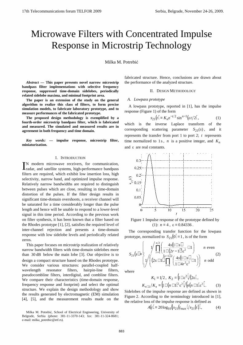
The unloaded Q-factor is presented as a function of microstrip line width (Figure 11), for the hairpin resonator. The curve is computed for the next dimensions of the hairpin resonator: mm85.22=l and mm75.10 =d . The
space between the two arms is about h3 to make the undesirable coupling weak enough. The initial resonator width is mm05.1=w .
For the combline realization, lumped SMD capacitors (Accu-F/Accu-P 0805) have been chosen to have the same
887
capacitance F7,24321 µ==== CCCC . The Q-factor of
the SMD capacitor is about 100 at the center frequency ( GHz2 ). The curves of unloaded Q-factor are computed
for the lossless capacitor ( ∞→CQ ) and for the real
capacitor with 100=CQ , Figure 12. The length of the
combline resonator is mm6=l . The initial resonator
width is mm1.2=w . For this value, the unloaded Q-
factor of the whole resonator is 113 when 100=CQ .
0.6 0.7 0.8 0.9 1 1.1 1.2120
130
140
150
160
170
w [mm]
fact
or,
qua
lity
U
nlo
ade
dQ
mm75.10 =dw
0d
Figure 11 Design curves of unloaded quality factor for
the hairpin resonator.
1.5 1.6 1.7 1.8 1.9 2 2.1 2.2 2.3 2.480
100
120
140
160
180
200
w [mm]
QC → inf
QC=100
w
C
fact
or,
qu
ality
Unl
oa
ded
Q
Figure 12 Design curves of unloaded quality factor for
the combline resonator.
Coupling coefficients and external quality factors of the resonators are computed as described in (9): 051.02,1 =k ,
079.03,2 =k , 145.04,3 =k , 71.181 =Q , 11.64 =Q . A full-
wave EM simulator is utilized to extract Q (Figures 13
and 14) and k (Figures 15 and 16). The initial dimensions of the hairpin filter (Figure 9),
according to the design curves shown in Figures 13 and 15, follow: mm3.012 =d , mm68.023 =d , mm43.034 =d ,
mm15.045 =d , mm06.056 =d , for the equal resonator
widths, mm05.1=w , mm75.10 =d , and for the equal
feed line widths mm15.0061 === www .
The initial dimensions of the combline filter (Figure 10), according to the design curves shown in Figures 14 and 16, follow: mm7.012 =d , mm4.023 =d , mm1.034 =d , for
the equal resonator widths, mm1.2=w . The tapped lines
dimensions are mm20 =l and mm350 =Ωl , and their
positions from the short-circuited end are mm4,21t =l and
mm54t =l .
Figure 13 Design curves of external quality factor for
the hairpin-line bandpass filter.
2 2.5 3 3.5 4 4.5 5 5.5 660
5
10
15
20
25
wtl
0Z
C
]mm[tl
mm1.2=w
fact
or,
qual
ity
E
xte
rnal
Q
Figure 14 Design curves of external quality factor for
the combline bandpass filter.
0 0.1 0.2 0.3 0.4 0.5 0.6 0.70.04
0.06
0.08
0.1
0.12
0.14
0.16
0.18
0.2
d [mm]
Co
uplin
g c
oef
ficie
nt,
M
ww
d
mm05.1=wmm75.10 =d
0d 0d
t,
coe
ffici
en
C
oupl
ing
k
Figure 15 Design curve of coupling coefficient for the
hairpin-line bandpass filter.
The photographs of the fabricated filters and layouts resulting from the optimization design are shown in Figure 17 and 18.
The hairpin filter dimensions are (Figure 9): mm3.01 =w , mm12 =w , mm15.13 =w , mm1.14 =w ,
mm6.05 =w , mm2.06 =w , mm2.012 =d ,
888
mm65.023 =d , mm5.034 =d , mm2.045 =d ,
mm15.056 =d , mm85.22=l , mm5.00 =l ,
mm6.10 =d , mm1.150 =Ωw .
The combline filter dimensions are (Figure 10): mm1.21 =w , mm1.22 =w , mm1.23 =w , mm8.14 =w ,
mm55.012 =d , mm25.023 =d , mm05.034 =d ,
mm7.5=l , mm20 =l , mm350 =Ωl , mm35,21t =l
mm05,54t =l , mm1.150 =Ωw .
0 0.2 0.4 0.6 0.8 10
0.025
0.05
0.075
0.1
0.125
0.15
0.175
0.20.2
d [mm]
C C
w w
t,
coe
ffici
en
C
oupl
ing
k dmm1.2=w
Figure 16 Design curve of coupling coefficient for the
combline bandpass filter.
Figure 17 Photograph and layout of the hairpin filter.
Figure 18 Photograph and layout of the combline filter.
The both structures are housed in a metal box and the distance between the top cover and dielectric is mm6 .
Joint optimization of the insertion loss and the return loss in the passband, the rejection in the stopband, and time-domain sidelobes, has been performed to achieve the desired specification in both frequency and time domain. The optimization error function (objective) is computed as the difference of the LC bandpass response and the realized structure response. First, the frequency response has been optimized to refine the initial insertion loss and return loss. Next, the relative loss has been optimized jointly with the frequency response, to achieve the sidelobe suppression more than dB30 down the main lobe. The
spurious sidelobe between the main lobe and the first sidelobe has been suppressed by slightly different resonators widths. The passband insertion loss and footprint area have been minimized by optimization of the
resonator dimensions as line width or spacing between two arms of the hairpin resonator.
The fabricated hairpin and combline filter have footprint of gg λ17.0λ25.0 × ( mm15.45 mm22.85 × ) and
gg λ24.0λ1.0 × ( mm22.4 mm9 × ) respectively, where
gλ is the guided wavelength of a Ω50 line on the
substrate at the center frequency. The filters are measured using an Agilent E5062A
network analyzer. The structures have been enclosed with the aluminum housing to eliminate the problem of “leaking connectors”. Radiated coupling tends to be dominated by cable emissions, rather than by direct radiation from the PCB, so a well-shielded enclosure minimizes “leakage” of the energy from the electromagnetic field and hence reduces conducted emissions.
The simulated and measured response of the hairpin filter is shown in Figures 19 and 20 and for the combline filter in Figures 21 and 22. Measured results have validated the theoretical analysis well.
Figure 19 Scattering parameters: EM simulation and
experiment for the hairpin-line bandpass filter.
Figure 20 Relative loss of EM simulation and experiment
for the hairpin-line bandpass filter ( dB381 =A ,
dB712 =A , ns33.4max =t , ns151 =t , ns23.52 =t ).
The hairpin filter has an insertion loss of dB2 at the
center frequency ( GHz98.1 ) due to the conductor and
dielectric losses. The conductor losses dominate. The experimental curve has an asymmetric sidelobe around
ns24.52 =t , which is caused by the fabrication deviation
889

of the hairpin filter and its housing. The combline filter has an insertion loss of dB4.3 at
the center frequency ( GHz87.1 ) due to the conductor,
dielectric losses, losses of SMD capacitors, and losses caused by the fabrication of vias. The losses of SMD capacitors dominate. The center frequency deviation is caused by the tolerance of SMD capacitance of pF25.0± .
The experimental curve has symmetric sidelobes.
0 0.5 1 1.5 2 2.5 3-50
-40
-30
-20
-10
0
f [GHz]
S11
[dB] Eksperiment
S21
[dB] Eksperiment
S11
[dB] EM
S21
[dB] EM
Experiment
Experiment
Figure 21 Scattering parameters: EM simulation and
experiment for the combline bandpass filter.
0 10 20 30 40 50-100
-80
-60
-40
-20
0
t [ns]
A(t
) [d
B]
EksperimentEMExperiment
1А
2А
maxt 1t 2t
]d
B[
loss
R
ela
tive
),(t
A
Figure 22 Relative loss of EM simulation and experiment
for the combline bandpass filter ( dB08,311 =A , dB582 ≈A , ns83,3max =t , ns17,131 =t ,
ns17,222 =t ).
VI. CONCLUSION
We have studied realizations of narrow bandpass filters with concentrated impulse response in time.
The novel realization of the coupled resonator filter has been modeled with immittance inverters. In this model, coupling between resonators has been frequency independent.
We have found that the combline filter has been the most suitable structure to meet all the design requirements simultaneously with the minimal footprint area.
On the other hand, the hairpin-line filter, free of lumped components and via-hole grounds, has been the most suitable one for the microstrip implementation. We have considered various microstrip structures and found that the
hairpin filter has had the minimal insertion loss in the passband and the minimal deviation from the specified center frequency.
Joint optimization of the insertion loss and the return loss in the passband, the rejection in the stopband, and sidelobe suppression, has been performed to achieve the desired specification in both frequency and time domain. The filter layout has been kept compact with minimal footprint and the coupling has been held under control.
Designed methodology has been presented and validated by EM simulation. Filters have been fabricated, measured, and the experimental results are in good agreement with the theoretical and simulation results. Our future research directives might be towards the design of similar filters with transmission zeros.
ACKNOWLEDGEMENT
This work was supported by the Serbian Ministry of Science and Technological Development under grant ET-11021.
REFERENCES
[1] J. D. Rhodes, “Prototype filters with a maximally flat impulse response,” International Journal of Circuit Theory and Applications, vol. 17, no. 4, pp. 421–427, 1989.
[2] M. M. Potrebić and D. V. Tošić, “Selective bandpass filter with concentrated impulse response,” Microwave and Optical Technology Letters, vol. 50, no. 11, pp. 2772–2777, Nov. 2008.
[3] M. M. Potrebić, “Microwave filters with concentrated impulse response in microstrip technology,” Ph.D. dissertation, School of Electrical Engineering, University of Belgrade, Belgrade, Serbia, 2009.
[4] D. V. Tošić, M. Potrebić, “Microwave Software Tools for Research and Education”, Microwave Review, vol. 12, no. 2, pp. 45–54, Nov. 2006.
[5] M. Potrebić, D. V. Tošić, “Comparison of WIPL-D Microwave and Microwave Office Software”, in Proc. 50th ETRAN Conf., Belgrade, Serbia, June 6–8, 2006, vol. IV, pp. 311–314.
[6] D. V. Tošić, M. Potrebić, “Symbolic analysis of immittance inverters”, in Proc. 14th Telecommunications forum TELFOR 2006, Belgrade, Serbia, Nov. 21–23, 2006, pp. 584–587.
[7] J.-S. Hong and M. J. Lancaster, Microstrip Filters for RF/Microwave Applications. New York: Wiley, 2001.
[8] A. R. Djordjević, M. D. Djurić , D. V. Tošić , and T. K. Sarkar, “On compact printed-circuit transmission lines,” Microwave and Optical Technology Letters, vol. 49, no. 11, pp. 2706–2709, Nov. 2007.
[9] A. R. Djordjević, M. B. Baždar, R. F. Harrington, and T. K. Sarkar, LINPAR for Windows: Matrix Parameters for Multiconductor Transmission Lines, Version 2.0 (Software and User's Manual). Boston: Artech House, 1999.
[10] E. G. Cristal and S. Frankel, “Hairpin-line and hybrid hairpin-line/half-wave parallel-coupled-line filters,” IEEE Transactions on Microwave Theory and Techniques, vol. 20, no. 11, pp. 719–728, Nov. 1972.
[11] D. Zhang, G.-C. Liang, C. F. Shih, R. S. Withers, M. E. Johansson, and A. D. Cruz, “Compact forwardcoupled superconducting microstrip filters for cellular communication,” IEEE Transactions on Applied Superconductivity, vol. 5, no. 2, pp. 2656–2659, Jun 1995.
[12] G. Mattaei, L. Young, and E. M. T. Jones, Microwave Filters, Impedance-Matching Networks, and Coupling Structures. New York: McGraw-Hill, 1964.
[13] D. G. Swanson, Jr., “Narrow-Band Microwave Filter Design,” IEEE Microwave Magazine, vol. 8, no. 5, pp. 105–114, Oct. 2007.
890