micro/nano and precision manufacturing technologgppies and
TRANSCRIPT

The 4th China-American Frontiers of Engineering Symposium
Micro/nano and precision manufacturing technologies and applicationsg pp
Dazhi WangDazhi Wang
School of Mechanical EngineeringDalian University of Technology
2015. 06. 01Irvine, US
Contact: [email protected]

Outline
Research backgroundResearch background
Research challenges
Research progress
Cross-scale manufacturing technology
E Jet micro/nano print patterningE-Jet micro/nano print-patterning
Ultra precision grinding and chemical mechanical polishing t h l itechnologies

Research background
Made in China 2025
Premier Li Keqiang advanced the"Made in China 2025" concept inhis Government Work Reporthis Government Work Report.
The major areas include: Biomedicine and high-performance medical apparatusInformation technologygyAerospace and aviation equipmentAdvanced rail equipment ……………..……………..
Manufacturing of high-performance parts and devices play an important roledevices play an important role.

Research challenges of high-performance parts and devices
The size has been decreased to micro- and nano-scale.The shape and structure become more complex and precise.The shape and structure become more complex and precise.The machining accuracy has been improved continuously.The material scope has been increased continuously.
Silicon waferMicrofluidic chips Grephene sensorFlexible electronics
It is difficult to satisfy the requirements of these parts and
Silicon waferp pFlexible electronics
devices using conventional manufacturing technologies.
Research progress
Cross-scale manufacturing technology
E-Jet micro/nano print-patterning
Ult i i i di d h i lUltra precision grinding and chemicalmechanical polishing technologies

Cross-scale manufacturing technology
Microfluidic chips have broad application prospects in rapiddiagnosis of major diseases and personalized medicine.Micro-nano cross-scale structure and nano-structure are neededfor special function such as filtering, block flowing.
Microfluidic chips for diagnosis of myocardial infarction
Genome mapping on nanofluidic chips(Nature Biotechnology, 2012)
Controllable manufacturing of micro-nano cross-scale structure andKey difficulties
special area nano-structure.

Cross-scale manufacturing technologyA composited fabrication method based on plasma etching andnanoparticle assembly was proposed.Microchannel nanochannel and modified biological sample wereMicrochannel, nanochannel and modified biological sample wereintegrated fabricated.A high quality nanofluidic sensing of biotin was achieved, theg q y gconcentration of 1 aM can be detected.
Fabrication of nanochannelsand Ag microelectrodes
Layout of the NPC-based nanofluidic biosensor Micro- and nano-channel and test result
Biosensors and Bioelectronic, 2015

Cross-scale manufacturing technologyAn integration of hot embossing and inverse UV photolithography isdeveloped to fabricate micro and nanochannels.A complete SU 8 nanofluidic chip was fabricated with a replicationA complete SU-8 nanofluidic chip was fabricated with a replicationprecision of 99.5%.
Process flow of the 2D nano-mold fabrication SU-8 micro and nanochannels fabrication
130 nm wide,150 nm high, 4 mm long
Lab on a chip, 20142D silicon nano-mold The thermally bonded nanochannels
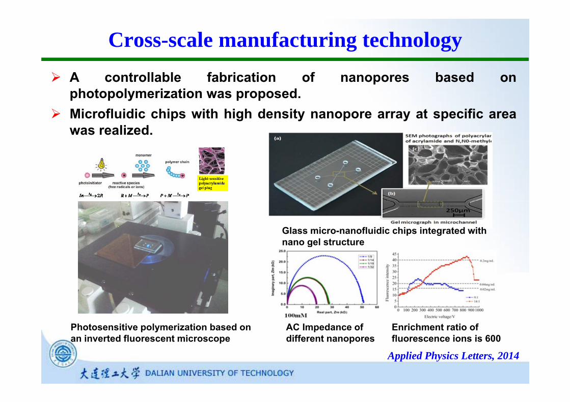
Cross-scale manufacturing technologyA controllable fabrication of nanopores based onphotopolymerization was proposed.Mi fl idi hi ith hi h d it t ifiMicrofluidic chips with high density nanopore array at specific areawas realized.
Glass micro-nanofluidic chips integrated with nano gel structureg
Photosensitive polymerization based on an inverted fluorescent microscope
Enrichment ratio of fluorescence ions is 600
AC Impedance of different nanoporesan inverted fluorescent microscope fluorescence ions is 600different nanopores
Applied Physics Letters, 2014

Cross-scale manufacturing technology
Disease diagnosis microfluidic chipsCooperated with CapitalBio Corporation detection of respiratoryCooperated with CapitalBio Corporation, detection of respiratorytract bacteria.Simultaneously detect 13 kinds of bacteria, detecting time reducedfrom 2 days to 3 hours, it is in clinical test now.
24 channel radial microchip I th l lifi ti & l ti24-channel radial microchip Isothermal amplification & real-time fluorescent detector

E-Jet micro/nano print-patterningMulti-layer composite element commonly exists in MEMS devices,which are widely used in energy, information, medical treatment, etc.The performance of multi-layer composite MEMS devices wasThe performance of multi-layer composite MEMS devices wasdetermined by their material composition and microstructure.
Controllable fabrication of material and structural compositedKey difficulties
Controllable fabrication of material and structural compositedfabrication.

E-Jet micro/nano print-patterningPrint-patterning is an effective way to obtain the material andstructural composited fabrication.
Print-patterning is an additive manufacturing method and has theadvantages of no mask, non-contact, no pressure and low cost.
Fl i d f tiFlowing deformation
JettingPattern
Droplet flying
FlyingSubstrate
Pattern
Deposition
Solidification
PatterningPrint-patterning process
MEMS devices

E-Jet micro/nano print-patterning
Electrohydrodynamic effect was used tod l i t tt i t h l
InkNeedle
develop a new print-patterning technology.
Electrohydrodynamic jet (E-Jet) print-patterning makes use of electrical and
Substrate Jetpatterning makes use of electrical andmechanical forces to form a fine liquid jetand droplets.
Movement stage
E-Jet print-patterning
Phenomenon of electrohydrodynamic effectPhenomenon of electrohydrodynamic effect

E-Jet micro/nano print-patterning
Droplet diameter can
Advantages of E-Jet print-patterning
High resolution Droplet diameter can be at nano-scale
Low requirement of Droplet size is much ll th dl Composite film depositionq
needle and ink smaller than needle size: less than 1/100
Strong Droplets are charged
Composite film deposition
controllability Droplets are charged
Suitable for different substrates Non-contact patterning
Mi / t tMicro/nano structure direct writing
E-Jet micro/nano print-patterning
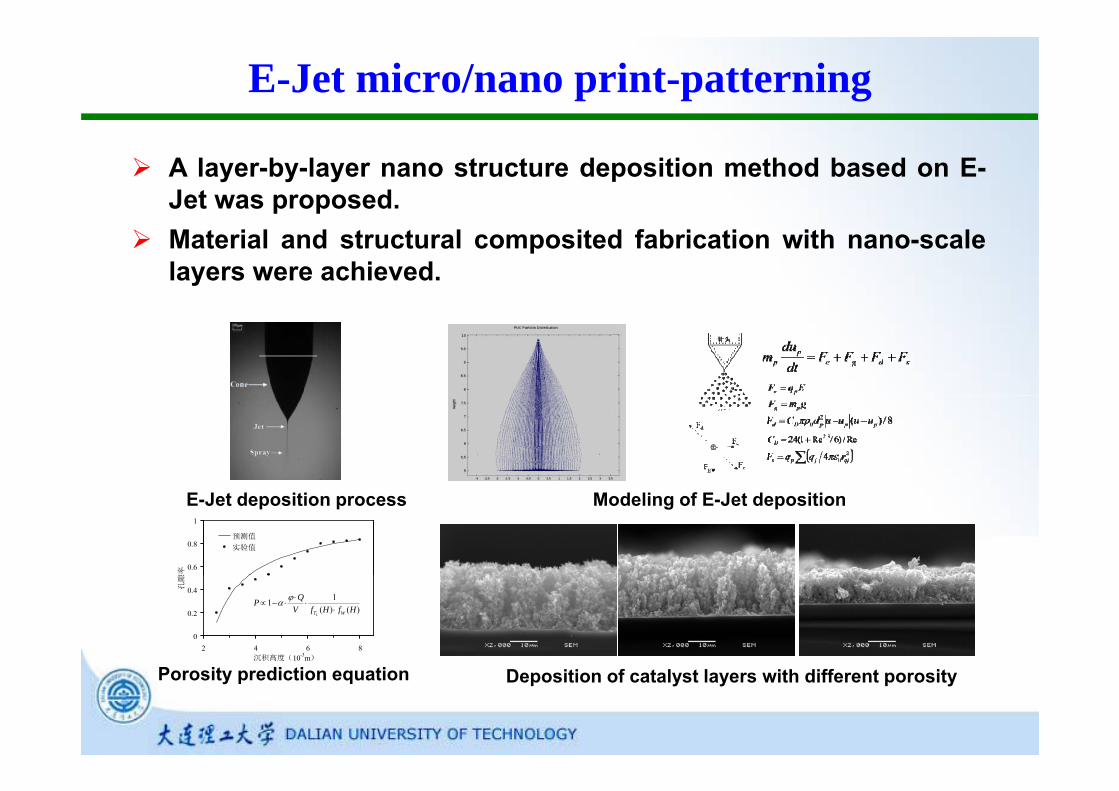
A layer-by-layer nano structure deposition method based on E-Jet was proposed.Material and structural composited fabrication with nano-scalelayers were achieved.
0.6
0.8
1
隙率
预测值
实验值
Modeling of E-Jet depositionE-Jet deposition process
0
0.2
0.4
2 4 6 8沉积高度(10-3m)
孔隙
)()(11
HfHfVQP
WTL⋅
⋅⋅
⋅−∝ϕα
Deposition of catalyst layers with different porosityPorosity prediction equation

E-Jet micro/nano print-patterning
Template-assisted E-Jet deposition method combined withembossing sacrificial layer technology was developed.Complex microstructures with high side wall angle and highaspect ratio were achieved.
Template-assisted E-Jet P tt d PZT thi k fil
Patterned graphene structuresTemplate assisted E Jet
deposition processPatterned PZT thick film
structures J. Eur. Ceram. Soc., 2012
E-Jet micro/nano print-patterning
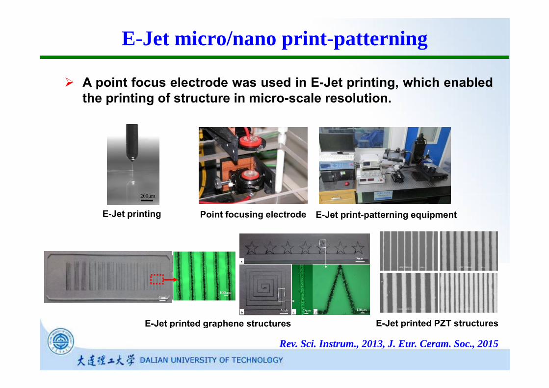
A point focus electrode was used in E-Jet printing, which enabledthe printing of structure in micro-scale resolution.
200μm
E-Jet printing Point focusing electrode E-Jet print-patterning equipment
E-Jet printed graphene structures E-Jet printed PZT structuresE Jet printed graphene structures E Jet printed PZT structures
Rev. Sci. Instrum., 2013, J. Eur. Ceram. Soc., 2015

E-Jet micro/nano print-patterning
An integrated MEA was developed, the common delaminationbl l d d th li bilit f th d i i d
Micro fuel cell: integrated MEA
problem was solved, and the reliability of the device was improved.The catalyst layer with material and structure gradient variation wasdeveloped, the catalyst utilization was improved.
0.4
ariz
atio
n / V
p , y p
0.0 0.1 0.2 0.3
0.2
0.3
IR c
orre
cted
ano
de p
ola
2
MEA1 MEA2 MEA3
Current density / A cm-2
0.5
0.6
0.7
50
60
70
80
Power
Gas-liquid two-phase model Mass transferring process Modeling of cell performance
0 50 100 150 200 250 3000.0
0.1
0.2
0.3
0.4
MEA-1 MEA-2 MEA-3
Current density (mA⋅cm-2)
Vol
tage
(V)
0
10
20
30
40
50 r density (mW
⋅cm-2)
Structure of integrated MEAIntegrated MEA after life test Cell performance testJ. Power Sources, 2013, Fuel cells , 2014

E-Jet micro/nano print-patterning
Annular array high frequency piezoelectric ultrasonic transducerHigh frequency ultrasonic transducer
was designed and developed, which achieved a workingfrequency of 70 MHz.
Annular array high frequency ultrasonic t d
Measurement of high frequency ultrasonic t dtransducers transducers
pie oelectric micro transformer Measurement of transformerpiezoelectric micro transformer Measurement of transformer
Sens. Actuator A-Phys. 2014

Ultra precision grinding and chemical mechanical polishing technologies
Ultra precision grinding and chemical mechanical polishingtechnologies are widely used for obtaining ultra flat and ultra smoothsurface such as blank wafer flattening wafer back thinningsurface, such as blank wafer flattening, wafer back thinning.
Blank wafer flattening Wafer back thinning
large size, nano-scale flatness, sub-nm roughness, lowresidual stresses and damage free
Key difficulties
residual stresses and damage-free.

Ultra precision grinding and chemical mechanical polishing technologies
A new ultra precision and low damage grinding technology with soft abrasive g g gygrinding wheel was developed.Ultra smooth and low damage ground surface wafer was produced Grinding mechanism Developed SAGWsurface wafer was produced. Grinding mechanism
of SAGWDeveloped SAGW
Damage depth 170nm Ra= 3.8nm
The wafer ground with diamond grinding wheel
Damage depth 10nm Ra= 0 7nm
The wafer ground with SAGW
10nm Ra= 0.7nm

Ultra precision grinding and chemical mechanical polishing technologies
A full-automatic grinder was developed for 300 mm wafer.A ultra precision wafer grinding-polishing machine was developed.
Principle and process of back thinning integrated grinding and polishing for wafer with outer rim
The first automatic ultra precision grinding machine for 300 mm wafer grinding in China
grinding and polishing for wafer with outer rim
Silicon wafer Sapphire wafer SiC window Optical windowUltra precision wafergrinding-polishingmachine (2-spindle,2-worktable )
Comparison of thinned waferwith and without outer rim
o tab e )Thinned wafer thickness<50μm,Ra<5nm

Ultra precision grinding and chemical mechanical polishing technologies
KDP is soft-brittle, temperature sensitive, dissolved in water,which is a difficult-to-machine materials.Abrasive-free polishing slurry with water molecular cluster wasdeveloped.Ult th d d f f bt i d i iUltra smooth and damage-free surface was obtained using microwater-dissolution and mechanical action of polishing pad.
pad
Waterl
Water-cluster brocken
Natural dissolutionKDP slurry
cluster
Developed li hi lpolishing slurry
Water-dissolution polishing surface

SummaryMicro-nano cross-scale manufacturing technologieswere introduced, microfluidic chips for disease, pdiagnosis and biosensing were produced.
E-Jet micro/nano print-patterning technique andequipment were developed, which enables the materialand structural composited manufacturing at micro/nanoscale.
Ultra precision grinding and chemical mechanicalli hi t h l i i t d d lt thpolishing technologies were introduced, ultra smooth
and low damage surface wafer was produced.

AcknowledgmentsMany thanks for the support from:

You are welcome to visit us at DLUT!You are welcome to visit us at DLUT!