micro- and nano-fabrication - unibas.ch other acceptors: b, al e.g.: ... • n-channel mos device in...
TRANSCRIPT

Michel Calame
Dpt. of Physics & Swiss Nanoscience Institute
web: http://calame.unibas.ch/
Micro- and nano-fabrication
Nano III
nanofabrication: tools for nanoscale devices
electronics
opticsopto-electronics
mechanics
NB: needs for research needs for industrial production

Nanofabrication, Nano III / mc / 3
Outline
• Introduction:
overview, state of the art
a bit of semiconductor physics ( CMOS)
• Fabrication basics
– IC fabrication overview
– clean-rooms
– Silicon: from sand to wafer
– material deposition techniques
– etching
– lithography
– examples of devices: MEMS, NEMS
• Outlook: new and future techniques
Nanofabrication, Nano III / mc / 4
References
overview books
• Fundamentals of Microfabrication: The Science of Miniaturization M. Madou, 2nd ed., CRC Press, 2002
• Nanoelectronics and Information Technology R. Waser ed., Wiley-VCH, 2012

Nanofabrication, Nano III / mc / 5
Introduction
http://ei.cs.vt.edu/~history/ENIAC.Richey.HTML
ENIAC, 1946 (18,000 vacuum tubes)
U. Penn.
Nanofabrication, Nano III / mc / 6
Introduction
1947, 24th December
John Bardeen
Walter Brattain
William Schockley
first point contact transfer resistor
Bell labsBell labs nobel.se
ATT Bell Labs
Nobel 1956

Nanofabrication, Nano III / mc / 7
Introduction
1958
Jack Kilby, Texas Instruments
first IC (Integrated Circuit)
Nobel in 2000 (for the IC)
together with Alferov & Krömer (for work on information and communication technology)
C. Esser, Infineon
Nanofabrication, Nano III / mc / 8
Introduction
1961, Robert Noyce,
Fairchild Camera
first integrated circuit available as a monolithic chip
Planar technology
(Si substrate and Al lines)
C. Esser, Infineon

Nanofabrication, Nano III / mc / 9
Introduction
1971 Intel anounces the i4004 microprocessor
"a new era of integrated electronics"
2250 transistors, 10m technology, 108kHz
http://www.intel.com
Nanofabrication, Nano III / mc / 10
Introduction
1981
Intel i8088
29000 transistors, 3mtechnology, 8MHz
invention of the PC (personal computer)
IBM, A.Child, B.Gates
http://www.intel.com

Nanofabrication, Nano III / mc / 11
Introduction
http://www.intel.com
Nanofabrication, Nano III / mc / 12
Introduction
http://www.intel.com

Nanofabrication, Nano III / mc / 13
Introduction
http://www.pbs.org/transistor/
“The complexity for minimum component costs has increased at a rate ofroughly a factor of two per year. Certainly over the short this rate can beexpected to continue, if not increase. Over the longer term, the rate ofincrease is a bit more uncertain, although there is no reason to believe itwill not remain nearly constant for at least 10 years.”
Electronics, Vol. 38(8), 1965
1965, Gordon E. Moore
(co-founder Intel Corporation)
Nanofabrication, Nano III / mc / 14 M. Bohr, Intel
Introduction
Scaling trends
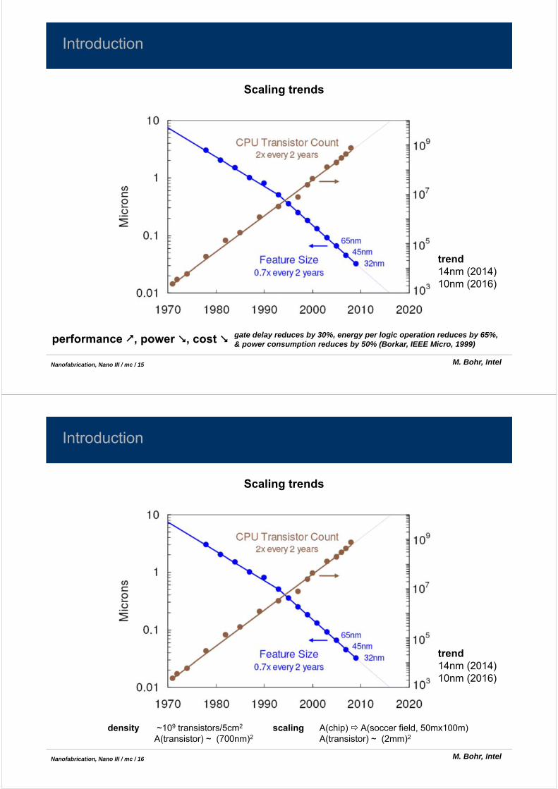
Nanofabrication, Nano III / mc / 15 M. Bohr, Intel
Introduction
Scaling trends
performance , power , cost gate delay reduces by 30%, energy per logic operation reduces by 65%, & power consumption reduces by 50% (Borkar, IEEE Micro, 1999)
trend14nm (2014)10nm (2016)
Nanofabrication, Nano III / mc / 16 M. Bohr, Intel
Introduction
Scaling trends
trend14nm (2014)10nm (2016)
density ~109 transistors/5cm2
A(transistor) ~ (700nm)2scaling A(chip) A(soccer field, 50mx100m)
A(transistor) ~ (2mm)2

Nanofabrication, Nano III / mc / 17
Introduction
J. Gobrecht, PSI
Nanofabrication, Nano III / mc / 18
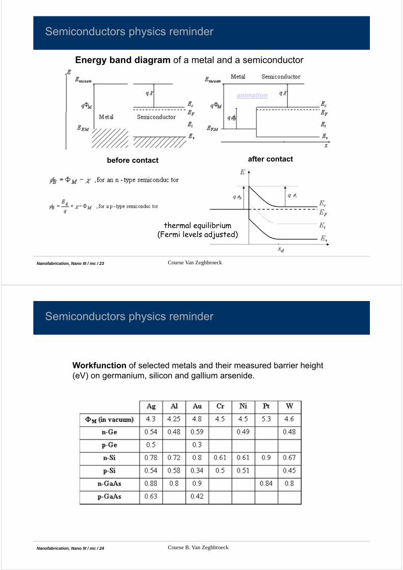
Introduction
top-down approach:
extend current techniques to smaller sizes
(EUV-L, x-ray lithography., nano-imprint, flip-up principle, i.e.: horizontal/vertical exchange, etc…)
problem: precision, costs
bottom-up approach:
start from individual atoms/molecules
use principles of self-organization (self-assembly; inspiration from biology, biochemistry, chemistry)
problem: long-range order difficult to achieve
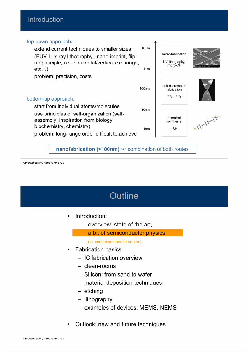
Nanofabrication, Nano III / mc / 19
Introduction
micro-fabrication
UV lithography, micro-CP
sub-micrometer fabrication
EBL, FIB
chemical synthesis
-SH
1 m
100nm
10nm
1nm
10 m
top-down approach:
extend current techniques to smaller sizes
(EUV-L, x-ray lithography., nano-imprint, flip-up principle, i.e.: horizontal/vertical exchange, etc…)
problem: precision, costs
bottom-up approach:
start from individual atoms/molecules
use principles of self-organization (self-assembly; inspiration from biology, biochemistry, chemistry)
problem: long-range order difficult to achieve
nanofabrication (<100nm) combination of both routes
Nanofabrication, Nano III / mc / 20
Outline
• Introduction:
overview, state of the art,
a bit of semiconductor physics
( condensed matter course)
• Fabrication basics
– IC fabrication overview
– clean-rooms
– Silicon: from sand to wafer
– material deposition techniques
– etching
– lithography
– examples of devices: MEMS, NEMS
• Outlook: new and future techniques

Nanofabrication, Nano III / mc / 21
Semiconductors physics reminder
Energy gaps
Si ~ 1.12 eVGe ~ 0.66 eVGaAs ~ 1.43 eV
NB: kT (RT) ~25meV
Nanofabrication, Nano III / mc / 22
Semiconductors physics reminder
Si atoms, intrinsicAs doped Sin-typeother donors: P, Sb
Ga doped Sip-typeother acceptors:B, Al
e.g.: resistivity changes by > 6 orders of mag. with a 1ppm B doping
Nanofabrication, Nano III / mc / 23
Semiconductors physics reminder
Energy band diagram of a metal and a semiconductor
Course Van Zeghbroeck
before contact after contact
thermal equilibrium (Fermi levels adjusted)
animation
Nanofabrication, Nano III / mc / 24
Semiconductors physics reminder
Workfunction of selected metals and their measured barrier height (eV) on germanium, silicon and gallium arsenide.
Course B. Van Zeghbroeck

Nanofabrication, Nano III / mc / 25
Semiconductors physics reminder
MOSFET technology: MOS capacitor
Ref. 3
Metal (gate) : Al (Mo, W, Cu), Poly-SiOxide : SiO2, d ≈ 1.7-10 nmSemiconductor : p- or n-type silicondoping 1013 - 1018 cm-3
orientation typ. <100>
energy band diagram Al/SiO2/p-Si
Nanofabrication, Nano III / mc / 26
Semiconductors physics reminder
MOS capacitor: ideal case
B. Föste, Infineon
Assumptions for the ideal MOS structure:1. No workfunction difference between metal and semiconductor (aligned vacuum and Fermi niveaus)2. charges at any bias exist only in thesemiconductor and at the metal surface3. no carrier transport through the oxide under dc-biasing conditions
i.e. Flat band condition at V=0(potential V between gate and back contact)

Nanofabrication, Nano III / mc / 27
Semiconductors physics reminder
B. Föste, Infineon
Real MOS structure:
flatband voltage <> 0 VFB=MS
MOS capacitor: real case
Nanofabrication, Nano III / mc / 28
Semiconductors physics reminder
MOS capacitor
B. Föste, Infineon
p-type semiconductor

Nanofabrication, Nano III / mc / 29
Semiconductors physics reminder
MOS capacitor
B. Föste, Infineon
Nanofabrication, Nano III / mc / 30
Semiconductors physics reminder
MOS capacitor
B. Föste, Infineon

Nanofabrication, Nano III / mc / 31
Semiconductors physics reminder
MOS capacitor
B. Föste, Infineon
Nanofabrication, Nano III / mc / 32
Semiconductors physics reminder
MOS capacitor
B. Föste, Infineon

Nanofabrication, Nano III / mc / 33
Semiconductors physics reminder
MOS capacitor
B. Föste, Infineon
gate voltage
control knob for charge carrier nature
(electron/hole) and density at
oxide/semiconductor interface
Nanofabrication, Nano III / mc / 34
Semiconductors physics reminder
MOSFET
B. Föste, Infineon

Nanofabrication, Nano III / mc / 35
Semiconductors physics reminder
B. Föste, Infineon
CMOS: complementary MOS, today’s most common technology
• n-channel MOS device in series with p-channel MOS device(when NMOS on, PMOS off and vice-versa, hence "complementary")
• simple design• draws very little current (except when switched on)• low-power technology
basic logic gate: inverter
• Vin high (1): NMOS on, PMOS off,
Vout=Vss (low, 0)
• Vin low (0): NMOS off, PMOS on,
Vout=Vdd (high, 1)
Nanofabrication, Nano III / mc / 36
Semiconductors physics reminder
CMOS: state-of-the-art
SOI substrate, Cu/low-k interconnection, 5 metal layers, features <0.13mm, 300mm wafers (12 ")
Refs 1 & 3 M. Bohr, Intel
Nanofabrication, Nano III / mc / 37
Semiconductors physics reminder
CMOS: state-of-the-art
gate structurevery thin oxide layers
SOI substrate, Cu/low-k interconnection, 5 metal layers, features <0.13mm, 300mm wafers (12 ")
Refs 1 & 3
Nanofabrication, Nano III / mc / 38 M. Bohr, Intel
Semiconductors physics reminder

Nanofabrication, Nano III / mc / 39 M. Bohr, Intel
Semiconductors physics reminder
NB: from planar geometryto 3D geometry (fin-FETs)also: gate all-aroundimprovement of substresholdswing, higher switching speed, lower power consumption
Nanofabrication, Nano III / mc / 40 http://www.intel.com/technology/silicon/index.htm
TEM cross-sections (Chau et al., Intel)
gate dielectric
state-of-the-art transistors: sub-50nm technology
Semiconductors physics reminder
Nanofabrication, Nano III / mc / 41
Outline
• Introduction:
overview, state of the art,
semiconductor physics reminder
• Fabrication basics
– IC fabrication overview
– clean-rooms
– Silicon: from sand to wafer
– material deposition techniques
– etching
– lithography
– examples of devices: MEMS, NEMS
• Outlook: new and future techniques
Nanofabrication, Nano III / mc / 42 H. Xiao, Ref.1
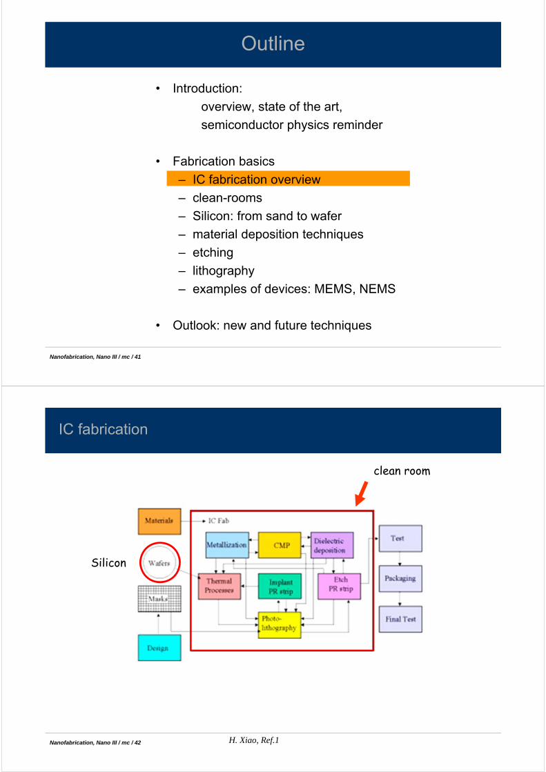
IC fabrication
clean room
Silicon
Nanofabrication, Nano III / mc / 43
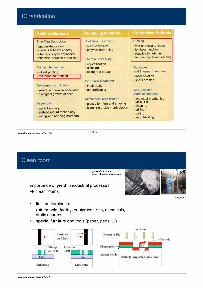
IC fabrication
Ref. 3
Nanofabrication, Nano III / mc / 44
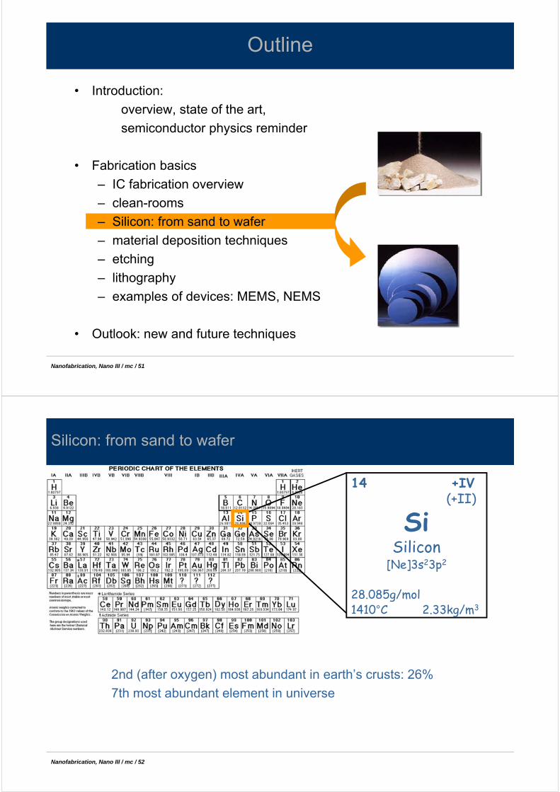
importance of yield in industrial processes
clean rooms
• limit contaminants
(air, people, facility, equipment, gas, chemicals, static charges, ….)
• special furniture and tools (paper, pens, ...)
Clean room
CMI, EPFL
grain of salt on a piece of a microprocessor

Nanofabrication, Nano III / mc / 45 H. Xiao, Ref.1
Clean room
clean room classes
class 1
less than 1 particle of diameter larger than 0.5m in a cubic foot
"normally clean" appartment:
typ. > 500’000 particles per cubic foot
outside air,
typ. ~ 3'000'000
(Federal Standard 209E)
Nanofabrication, Nano III / mc / 46
clean room standard (ISO 14644-1)
Cn = 10N (0.1 / D)2.08 Cn maximum permitted number of particles per m3
specified particle size (rounded)N ISO class number ( multiple of 0.1 and 9)D particle size (micrometers)
Classmaximum particles/ft³ ISO
equivalent≥0.1 µm ≥0.2 µm ≥0.3 µm ≥0.5 µm ≥5 µm
1 35 7 3 1 ISO 3
10 350 75 30 10 ISO 4
100 750 300 100 ISO 5
1,000 1,000 7 ISO 6
10,000 10,000 70 ISO 7
100,000 100,000 700 ISO 8
Clean room

Nanofabrication, Nano III / mc / 47
ParticleParticle Size(microns)
Beach Sand 100 - 10000
Pollens 10 - 1000
Textile Fibers 10 - 1000
Human Hair 40 - 300
Saw Dust 30 - 600
Tea Dust 8 - 300
Red Blood Cells 5 - 10
Spores 3 - 40
Coal Dust 1 - 100
Smoke from Synthetic Materials 1 - 50
Auto and Car Emission 1 - 150
Metallurgical Dust 0.1 - 1000
Humidifier 0.9 - 3
Copier Toner 0.5 - 15
Bacteria 0.3 - 60
Burning Wood 0.2 - 3
Tobacco Smoke 0.01 - 4
Viruses 0.005 - 0.3
Typical Atmospheric Dust 0.001 to 30
Clean room
Nanofabrication, Nano III / mc / 48
Clean room
H. Xiao, Ref.1
simple clean room design

Nanofabrication, Nano III / mc / 49
Clean room
H. Xiao, Ref.1
more advanced clean room design
Nanofabrication, Nano III / mc / 50
1. Store personal items.
2. Discard any gum, candy, etc.
3. Remove any makeup with cleanroom soap and water.
4. Take a drink of water to wash away throat particles.
5. Cover any facial hair with a surgical mask or beard/mustache lint-free cover.
6. Put on a lint-free head cover.
7. Clean shoes with shoe cleaners.
8. Put shoe cover on over shoes.
9. Clean any small, pre-approved items to be taken inside.
10. Pick up booties.
11. Sit on "dirty" side of bench.
12. Put on one bootie (over plastic shoe cover).
13. Swing bootied foot to "clean" side of bench.
14. Put on other bootie on "dirty" side.
15. Swing bootied foot to "clean" side.
16. Enter main gowning room.
17. Set aside badge, pager, and any other items to be taken inside.
18. Put on nylon gowning gloves.
19. Obtain bunny suit and belt from hanger.
21. If you've never done it before, putting on a bunny suit can take 30 to 40 minutes. The Intel pros can do it in five.
22. Put on bunny suit without letting it touch the floor.
23. Put on belt.
24. Tuck bunny suit pant legs into booties.
25. Fasten snaps at top of booties.
26. Attach filter unit to belt.
27. Attach battery pack to belt.
28. Plug filter unit into battery pack.
29. Obtain helmet, safety glasses, and ID badge from rack.
30. Put on helmet.
31. Tuck helmet skirt into bunny suit.
32. Zip up bunny suit at shoulders.
33. Attach helmet hose to filter unit.
34. Tighten knob at back of helmet.
35. Put on ID badge.
36. Put on pager.
37. Put on safety glasses.
38. Obtain disposable scope shield.
39. Remove protective covering from both sides of scope shield.
40. Undo front helmet snaps.
41. Attach face shield to helmet.
42. Re-snap front helmet snaps.
43. Examine attire in mirror.
44. Put on latex gloves.
45. Enter the cleanroom.
Steps to enter a cleanroom (Intel)
http://www.intel.com/
Clean room
Nanofabrication, Nano III / mc / 51
Outline
• Introduction:
overview, state of the art,
semiconductor physics reminder
• Fabrication basics
– IC fabrication overview
– clean-rooms
– Silicon: from sand to wafer
– material deposition techniques
– etching
– lithography
– examples of devices: MEMS, NEMS
• Outlook: new and future techniques
Nanofabrication, Nano III / mc / 52
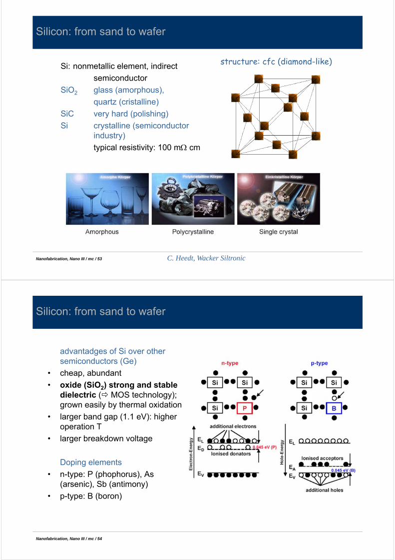
Silicon: from sand to wafer
2nd (after oxygen) most abundant in earth’s crusts: 26%
7th most abundant element in universe
14 +IV(+II)
SiSilicon
[Ne]3s23p2
28.085g/mol1410°C 2.33kg/m3
Nanofabrication, Nano III / mc / 53
Silicon: from sand to wafer
Si: nonmetallic element, indirect
semiconductor
SiO2 glass (amorphous),
quartz (cristalline)
SiC very hard (polishing)
Si crystalline (semiconductor industry)
typical resistivity: 100 m cm
structure: cfc (diamond-like)
C. Heedt, Wacker Siltronic
Nanofabrication, Nano III / mc / 54
Silicon: from sand to wafer
advantadges of Si over other semiconductors (Ge)
• cheap, abundant
• oxide (SiO2) strong and stable dielectric ( MOS technology); grown easily by thermal oxidation
• larger band gap (1.1 eV): higher operation T
• larger breakdown voltage
Doping elements
• n-type: P (phophorus), As (arsenic), Sb (antimony)
• p-type: B (boron)

Nanofabrication, Nano III / mc / 55
Silicon: from sand to wafer
C. Heedt, Wacker Siltronic
Si purification: natural Si oxide MGS EGS
metallurgical electronic grade
Nanofabrication, Nano III / mc / 56
Silicon: from sand to wafer
C. Heedt, Wacker Siltronic
Si purification: MGS EGS

Nanofabrication, Nano III / mc / 57
Silicon: from sand to wafer
C. Heedt, Wacker Siltronic
EGS single cristal ingot: CZ growth (Czochralski method)
Nanofabrication, Nano III / mc / 58
Silicon: from sand to wafer
C. Heedt, Wacker Siltronic
Si ingot
up to 300mm diameter (FZ or floating zone purer butlimited to 200mm)

Nanofabrication, Nano III / mc / 59
Silicon: from sand to wafer
Surface grinding
flat: up to 150mm
notch: > 200mm
mark crist. orient.
C. Heedt, Wacker Siltronic
Nanofabrication, Nano III / mc / 60
Silicon: from sand to wafer
C. Heedt, Wacker Siltronic
wafer sawing
edge rounding

Nanofabrication, Nano III / mc / 61
Silicon: from sand to wafer
Ref. 1
wafer finishing
• lapping
(global planarization, double-sided)
• wet etching , isotropic
(4:1:3 mixture of HNO3, HF and CH3COOH)
• CMP (chemical mechanical polishing)
• wet cleaning (RCA1, RCA2)
surface roughness after the various treatment
Nanofabrication, Nano III / mc / 62
Silicon: from sand to wafer
Ref. 1
wafer flats
• Orientation for automatic equipment
• Indicate type and orientation of crystal.
Primary flat – The flat of longest length located in the circumference of the wafer. The primary flat has a specific crystal orientation relative to the wafer surface.
Secondary flat – Indicates the crystal orientation and doping of the wafer. The location of this flat varies.
flat at 180 deg for n-type and 90 deg for p-type
flat at 45 deg for n-type, no secondary for p-type
www.ee.byu.edu/cleanroom
Nanofabrication, Nano III / mc / 63
Silicon: from sand to wafer
Ref. 1
Miller indices description of lattice planes and lattice directions in crystal
example cubic lattice system
the direction [hkl] defines a vector direction normal to surface of a particular plane or facet.
www.ee.byu.edu/cleanroom
type: <100>Equivalent directions:[100],[010],[001]
type: <110>Equivalent directions:[110], [011], [101],[-1-10], [0-1-1], [-10-1],[-110], [0-11], [-101],[1-10], [01-1], [10-1]
type: <111>Equivalent directions:[111], [-111], [1-11], [11-1]
Nanofabrication, Nano III / mc / 64
Outline
• Introduction:
overview, state of the art,
semiconductor physics reminder
• Fabrication basics
– IC fabrication overview
– clean-rooms
– Silicon: from sand to wafer
– material deposition techniques
– etching
– lithography
– examples of devices: MEMS, NEMS
• Outlook: new and future techniques
additivesubstractive

Nanofabrication, Nano III / mc / 65
Fabrication: physical deposition techniques
fundamentals of film deposition
• gas kinetics
(mean free path: small holes filling, residual gas atoms: purity)
• UHV (p<10-9 mbar) necessary depending on final purity needed
• phase diagrams of materials to deposit (pressure, temperature)
• control type of growth: homoepitaxy; heteroepitaxy; growth of polycristalline or amorphous layers;
importance of strain misfit dislocations
substrate temperature
Nanofabrication, Nano III / mc / 66
Fabrication: physical deposition techniques
• gas kinetics
(mean free path: small holes filling, residual gas atoms: purity)
table for residual air at 25°C
surface= 1cm2

Nanofabrication, Nano III / mc / 67
Fabrication: physical deposition techniques
• type of growth: homoepitaxy
IBM AlmadenSTM image, 28nm by 28nm area of the terraced copper and copper nitride surface with Manganese humps (1-10 atoms long).
Nanofabrication, Nano III / mc / 68
Fabrication: physical deposition techniques
• heteroepitaxy
small mismatch large mismatch
Frank-Van der Merwe Volmer-Weber Stranski-Krastanov
(layer growth; ideal) (island growth) (layers then islands due to strain build up)

Nanofabrication, Nano III / mc / 69
Fabrication: physical deposition techniques
• importance of strain misfit dislocations: T
strained layer
substrate
Nanofabrication, Nano III / mc / 70
Fabrication: physical deposition techniques
example of the importance of strain
Locquet, Perret et al., Nature 1998

Nanofabrication, Nano III / mc / 71
Fabrication: thermal evaporation
thermal evaporation: free, isotropic (Langmuir)
e-beam evaporation
• More complex, but extremely versatile.• T > ~ 3000°C• Use evaporation cones or crucibles (e.g. graphite) in a copper hearth.
• Typical emission voltage is 8-10 kV.• Exposes substrates to secondary electron radiation.(X-rays can also be generated by high voltage electron beam)
• Typical deposition rates are 1-100 Å/s• Common evaporant materials:– Everything a resistance heated evaporator will accommodate, plus:
– Ni, Pt, Ir, Rh, Ti, V, Zr, W, Ta, Mo– Al2O3, SiO, SiO2, SnO2, TiO2, ZrO2
Nanofabrication, Nano III / mc / 72
Fabrication: thermal evaporation
thermal evaporation: ~ directional
effusion (Knudsen) cellevaporation rate ~ controlled by temperature only(play with equilibrium vapor pressure and aperture size)
Kn=/d mean free path, d: orifice diameter
Kn>1 free molecular flowkn<<1 viscous flow
NB: distribution of vapor beam intensity; depends on ratio L/d (filling level of cell !)
Biasiol and Sorbia, 2001
p p*
Nanofabrication, Nano III / mc / 73
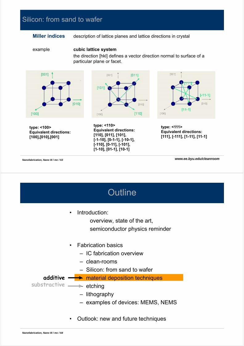
Fabrication: physical deposition techniques
NB: shadow effects / step coverage
directionality and adhesion effects
Springer Handbook of nanotechnology, Bushan ed., 2004
Nanofabrication, Nano III / mc / 74
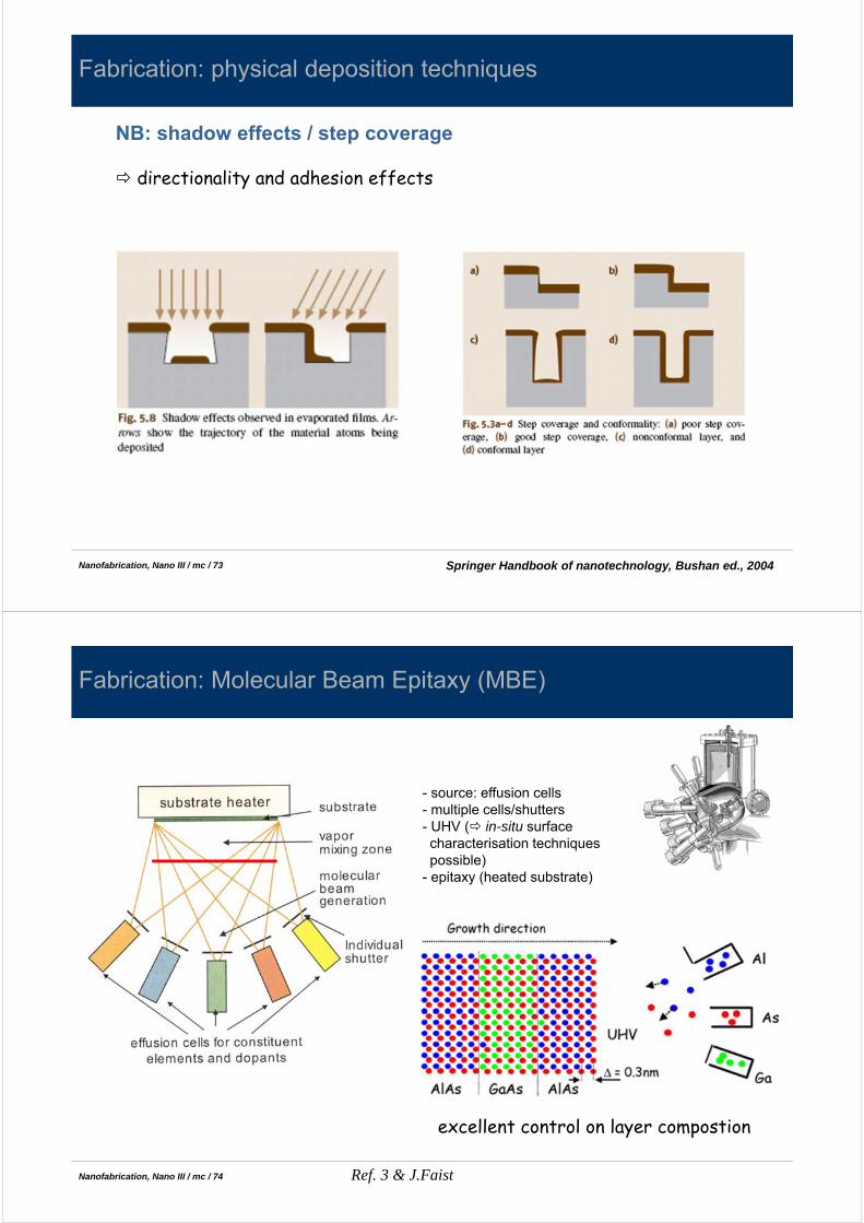
Fabrication: Molecular Beam Epitaxy (MBE)
Ref. 3 & J.Faist
excellent control on layer compostion
- source: effusion cells- multiple cells/shutters- UHV ( in-situ surface characterisation techniques possible)
- epitaxy (heated substrate)
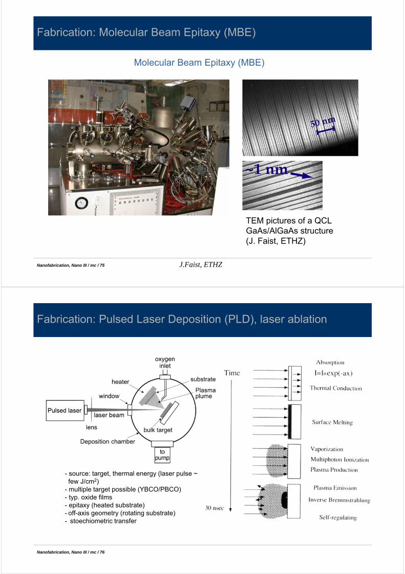
Nanofabrication, Nano III / mc / 75
Fabrication: Molecular Beam Epitaxy (MBE)
Molecular Beam Epitaxy (MBE)
J.Faist, ETHZ
TEM pictures of a QCLGaAs/AlGaAs structure(J. Faist, ETHZ)
Nanofabrication, Nano III / mc / 76
Fabrication: Pulsed Laser Deposition (PLD), laser ablation
- source: target, thermal energy (laser pulse ~ few J/cm2)
- multiple target possible (YBCO/PBCO)- typ. oxide films- epitaxy (heated substrate)- off-axis geometry (rotating substrate)- stoechiometric transfer

Nanofabrication, Nano III / mc / 77
Fabrication: Sputtering
DC sputtering
• few 100V plasma (p~10-1 - 10-3mbar)
• sputtering of target by ions, typ. Ar+
(binding energy of target atoms: 4-8eV; min energy of Ar+ ions: 20-50eV; multiple collisions necessary to get backward material)
• stoichiometry of target (~) preserved
• increase ionization rate of plasma with B-field (magnetron sputtering)
• insulating targets: RF-sputtering (~13MHz)
(erosion)
potential profile
Nanofabrication, Nano III / mc / 78
Fabrication: Chemical Vapor Deposition
Chemical Vapor Deposition (CVD)
def: reaction of chemicals (precursors, gas phase) at high T
to form the deposited thin film
SiO2 3 SiH4 + O2 SiO2 + 2 H2 450°C
SiO2 SiCl2H2 + 2N2O SiO2 + 2 N2 + 2HCl 900°C
Si3N4 3 SiH4 + 4NH3 Si3N4 + 12 H2 700°C-900°C
poly Si SiH4 Si + 2 H2 580-650°C, 1mbar
LPCVD: low-pressure CVD; requires higher temperaturesPECVD: plasma enhanced CVD, allows temperature reductionMOCVD: metal-organic CVD, use organometallic precursors
CMI, EPFL
note: stress can be critical (e.g. nitride layers)

Nanofabrication, Nano III / mc / 79
Fabrication: chemical deposition techniques
note: thermal oxidation (note really a deposition process, Si consumed during process)
better oxide quality, very low density of defects, homogeneous thickness (gate – insulating - material)
dry Si (solid) + O2 (gas) SiO2 (solid)
wet Si (solid) + H2O (steam) SiO2 (solid) + 2H2 (gas)
final thickness: few x 10Å to 2m (NB: native oxide layer: ~ 2nm)
T ~ 900°C – 1200°C
limited to materials able to form oxides
Nanofabrication, Nano III / mc / 80
Fabrication: chemical deposition techniques
thermal oxidation xox(t) [1+c(t+)]1/2
(Deal-Grove)
Nanofabrication, Nano III / mc / 81
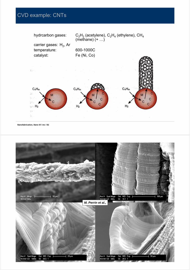
hydrcarbon gases: C2H2 (acetylene), C2H4 (ethylene), CH4 (methane) (+ …)
carrier gases: H2, Ar temperature: 600-1000C catalyst: Fe (Ni, Co)
CVD example: CNTs
Nanofabrication, Nano III / mc / 82
M. Perrin et al.,

Nanofabrication, Nano III / mc / 83
M. Perrin et al.,
applications: - composite materials- carbon-based super-capacitors
(large surface to volume ratio)- …
Nanofabrication, Nano III / mc / 84
self-limiting growth
Beneq
Fabrication: Atomic Layer Deposition (ALD)
material A
material B

Nanofabrication, Nano III / mc / 85
A: Hydroxylated surface
B: Trimethylaluminium (TMA) reacts with OH
C: TMA does not react with itself (passivation)
D: Purge reactor
Cambridge Nanotech
Fabrication: Atomic Layer Deposition (ALD)
example: deposition of Al2O3
Nanofabrication, Nano III / mc / 86
E: H2O removes CH3
and passivates
F: Purge reactor
G: Ready for new cycle
Repeat A-G for controlled monolayer deposition
Fabrication: Atomic Layer Deposition (ALD)
Cambridge Nanotech
~1.1Å/cycle
for Al2O3
Nanofabrication, Nano III / mc / 87
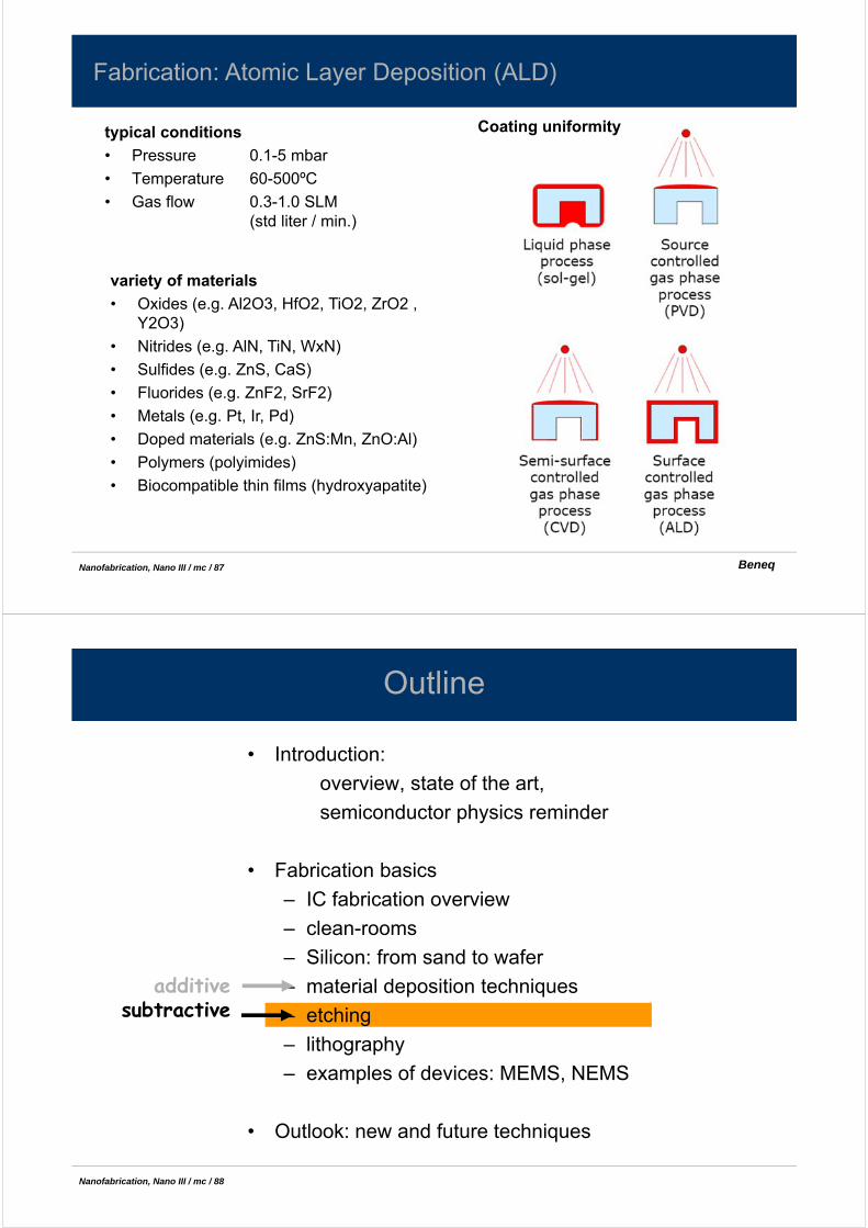
typical conditions
• Pressure 0.1-5 mbar
• Temperature 60-500ºC
• Gas flow 0.3-1.0 SLM (std liter / min.)
Fabrication: Atomic Layer Deposition (ALD)
variety of materials
• Oxides (e.g. Al2O3, HfO2, TiO2, ZrO2 , Y2O3)
• Nitrides (e.g. AlN, TiN, WxN)
• Sulfides (e.g. ZnS, CaS)
• Fluorides (e.g. ZnF2, SrF2)
• Metals (e.g. Pt, Ir, Pd)
• Doped materials (e.g. ZnS:Mn, ZnO:Al)
• Polymers (polyimides)
• Biocompatible thin films (hydroxyapatite)
Coating uniformity
Beneq
Nanofabrication, Nano III / mc / 88
Outline
• Introduction:
overview, state of the art,
semiconductor physics reminder
• Fabrication basics
– IC fabrication overview
– clean-rooms
– Silicon: from sand to wafer
– material deposition techniques
– etching
– lithography
– examples of devices: MEMS, NEMS
• Outlook: new and future techniques
additivesubtractive

Nanofabrication, Nano III / mc / 89
Fabrication: etching
Chemical:
• wet etching (can be anisotropic due to crystal-face selectivity)
• fast, up to 10m/min or more
Physical etching (sputtering)
• ion milling, FIB (focused ion beam)
• dry etching (plasma assisted techniques, pressures up to 10mbar)
(more a combination of physical and chemical material removal)
• slower, typ. 100Å -1000Å/min
key points:
selectivity (etch rates ratio of masking layer and layer to etch)
directionality (defines etch profile)
note:
CMP, chemical mechanical polishing to achieve global planarization
combine mechanical abrasion with chemical etching; key parameters: force, slurry type, pad velocity
Nanofabrication, Nano III / mc / 90 http://www.memsguide.com
Fabrication: wet etching
• use chemical solutions to dissolve material
• chemical species react with surface etch products rinse, dry
isotropic, typ. 10m/min
anisotropic, typ. 1m/min
Nanofabrication, Nano III / mc / 91
Fabrication: wet etching
SiO2 6:1, buffered in NH4F (BHF) or 10:1 to 100:1 (by vol.) HF in H2O
NB: 1:1 HF (49% HF in H2O) too fast
SiO2 + 6 HF H2SiF6 + 2 H2O (H2SiF6 soluble in H2O)
BHF etch rate: 1000Å/min (room temperature)
masks: photoresist, silicon nitride
!! HF is extremely agressive: use adequate protection gear !!
Si polycrystalline or single-crystal
isotropic: mix of HNO3 and HF
(cyclic process: HNO3 oxidizes Si, HF removes oxide)
Si + HNO3 + 6 HF H2SiF6 + HNO2 + H2O + H2
Nanofabrication, Nano III / mc / 92
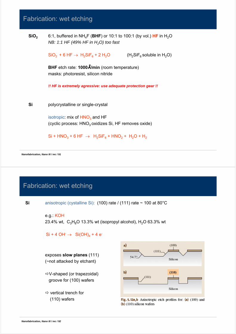
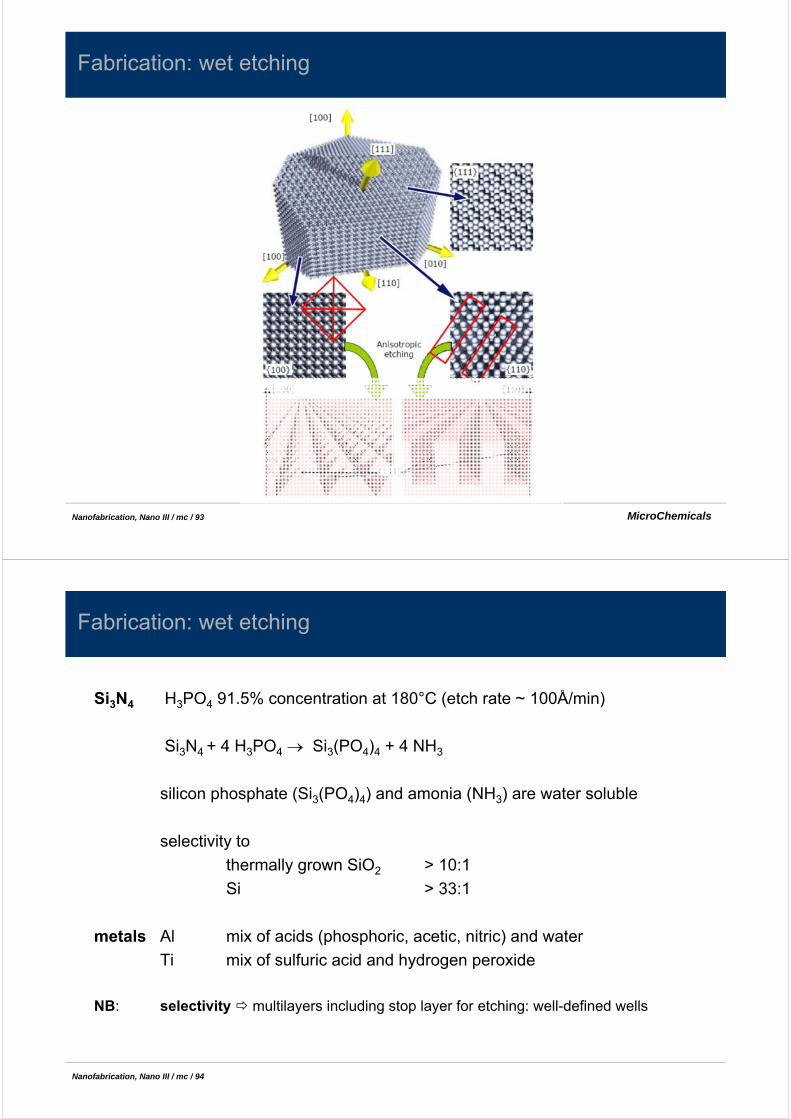
Fabrication: wet etching
Si anisotropic (cystalline Si): (100) rate / (111) rate ~ 100 at 80°C
e.g.: KOH
23.4% wt, C3H8O 13.3% wt (isopropyl alcohol), H2O 63.3% wt
Si + 4 OH- Si(OH)4 + 4 e-
exposes slow planes (111)
(~not attacked by etchant)
V-shaped (or trapezoidal)
groove for (100) wafers
vertical trench for
(110) wafers
(110)
Nanofabrication, Nano III / mc / 93
Fabrication: wet etching
MicroChemicals
Nanofabrication, Nano III / mc / 94
Fabrication: wet etching
Si3N4 H3PO4 91.5% concentration at 180°C (etch rate ~ 100Å/min)
Si3N4 + 4 H3PO4 Si3(PO4)4 + 4 NH3
silicon phosphate (Si3(PO4)4) and amonia (NH3) are water soluble
selectivity to
thermally grown SiO2 > 10:1
Si > 33:1
metals Al mix of acids (phosphoric, acetic, nitric) and water
Ti mix of sulfuric acid and hydrogen peroxide
NB: selectivity multilayers including stop layer for etching: well-defined wells

Nanofabrication, Nano III / mc / 95
Fabrication: dry etching
dry etching: usually plasma based
as compared to wet etch:
- smaller undercut (patterning of smaller lines)
- higher anisotropicity (high aspect-ratio structures possible)
- less selective
- mask etching not negligible
ion milling
purely physical
sputering by accelerated Ar+ ions
p ~ 10-4 – 10-3 torr;
etch rate: few nm/min
note: no selectivity
Nanofabrication, Nano III / mc / 96 http://www.memsguide.com
Fabrication: dry etching
RIE: reactive ion etchingphysical and chemical
Si etch with SF6
- accelerated ions (e.g.: Ar+, directional) either modify surface state (e.g.: bond breaking, makes surface more reactive) or help etch products to desorb
- reactive species (e.g. plasma generated from from SF6) diffuse to substrate surface and react, forming SiF4 (volatile)
SF5+
F-

Nanofabrication, Nano III / mc / 97 http://www.memsguide.com
Fabrication: dry etching
DRIE (key process for MEMS)
deep reactive ion etching
depth: up to few 100m
ICP RIE
SF6 alternated with C4F8 (to passivate walls), Bosch process
selectivity
Si:SiO2, 150:1
profile angle +/- 1°
Nanofabrication, Nano III / mc / 98
Fabrication: dry etching
Focused Ion Beam (FIB)
• controlled, directed heavy ion beam (typ. Ga)
• local ion milling (sputtering)
• fine structures, nm range
SEM/FIB (FEI Nova 600 nanoLab)
Electrons• High penetration depth• Low mass -> higher speed for given energy• Electrons are negative• Magnetic lens (Lorentz force)
Ions• High interaction probability, less penetration depth• Ions can remain trapped -> doping• High mass -> slow speed but high momentum milling !!!• Ions are positive• Electrostatic lenses
IBM
Nanofabrication, Nano III / mc / 99
Fabrication: dry etching
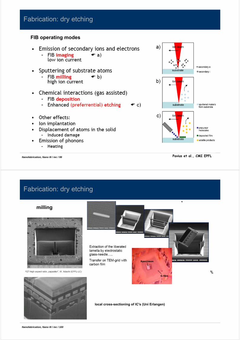
Pavius et al., CMI EPFL
FIB operating modes
Nanofabrication, Nano III / mc / 100
Fabrication: dry etching
Pavius et al., CMI EPFL
milling
local cross-sectioning of IC's (Uni Erlangen)

Nanofabrication, Nano III / mc / 101
Fabrication: etching, short summary
Chemical:
• wet etching (can be anisotropic due to crystal-face selectivity)
• formation of reaction products soluble in the etch solution or volatile at low pressures
Physical etching (sputtering)
• ion milling, FIB (focused ion beam)
• dry etching (plasma assisted techniques, pressures up to 10mbar)
(more a combination of physical and chemical material removal)
• relies on momentum transfer of particles hitting and eroding the surface
key points:
selectivity (etch rates ratio of masking layer and layer to etch)
directionality (defines etch profile)
Nanofabrication, Nano III / mc / 102
Outline
• Introduction:
overview, state of the art,
semiconductor physics reminder
• Fabrication basics
– IC fabrication overview
– clean-rooms
– Silicon: from powder to wafer
– material deposition techniques
– etching
– lithography
– examples of devices: MEMS, NEMS
• Outlook: new and future techniques
Nanofabrication, Nano III / mc / 103
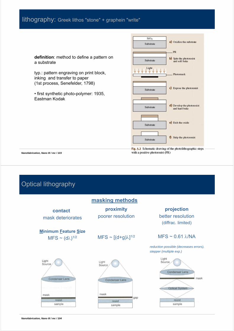
lithography: Greek lithos "stone" + graphein "write"
definition: method to define a pattern on a substrate
typ.: pattern engraving on print block, inking and transfer to paper(1st process, Senefelder, 1798)
• first synthetic photo-polymer: 1935, Eastman Kodak
Nanofabrication, Nano III / mc / 104
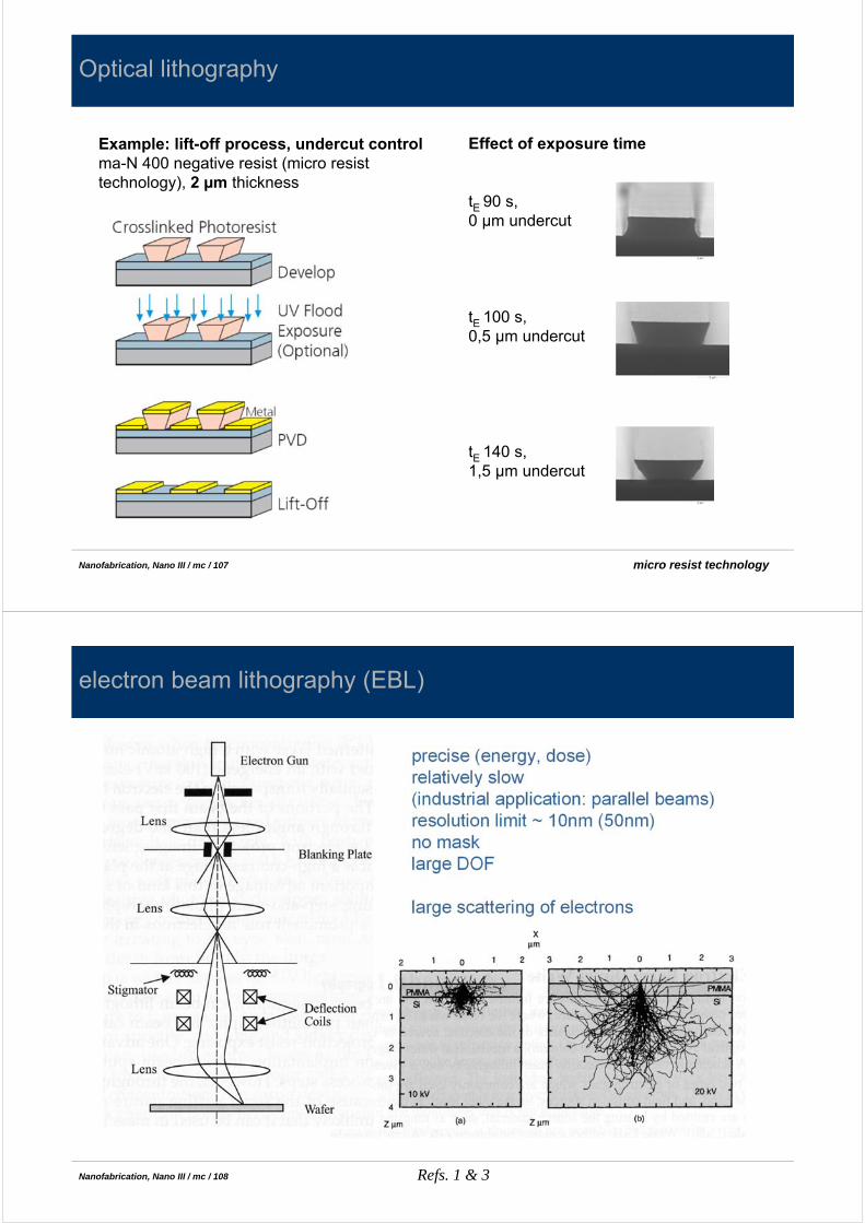
Optical lithography
masking methods
Ref. 3
contact
mask deteriorates
Minimum Feature Size
MFS ~ (d)1/2
proximity
poorer resolution
MFS ~ [(d+g)]1/2
projection
better resolution(diffrac. limited)
MFS ~ 0.61 /NA
reduction possible (decreases errors),
stepper (multiple exp.)

Nanofabrication, Nano III / mc / 105
Optical lithography
phase-shifting technique
destructive interference
Nanofabrication, Nano III / mc / 106
Optical lithography
photoresists profiles(after development)
Ref. 2
R: developing rate of exposed region
R0: developing rate of unexposed region
R/R0 > 10: fast developper
: resist contrast
(linked to exposure dose, cf Madou)
Nanofabrication, Nano III / mc / 107
Optical lithography
Example: lift-off process, undercut controlma-N 400 negative resist (micro resist technology), 2 µm thickness
micro resist technology
Effect of exposure time
tE 90 s,0 µm undercut
tE 100 s,0,5 µm undercut
tE 140 s,1,5 µm undercut
Nanofabrication, Nano III / mc / 108
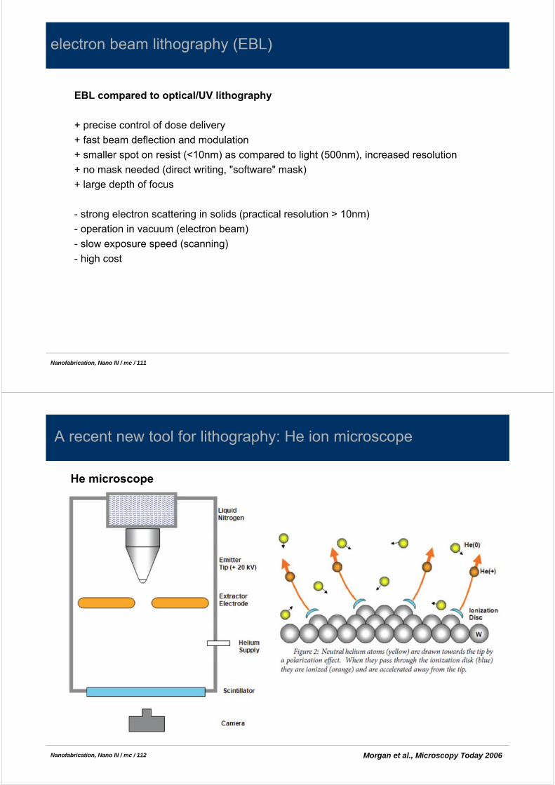
electron beam lithography (EBL)
precise (energy, dose)relatively slow (industrial application: parallel beams)resolution limit ~ 10nm (50nm)no masklarge DOF
large scattering of electrons
Refs. 1 & 3

Nanofabrication, Nano III / mc / 109
proximity effects
J. Gobrecht, PSI
electron beam lithography (EBL)
Nanofabrication, Nano III / mc / 110
electron beam lithography (EBL)
dose test on PMMA: overcut to undercut (A. Kleine) note: undercut critical for lift-off
Nanofabrication, Nano III / mc / 111
electron beam lithography (EBL)
EBL compared to optical/UV lithography
+ precise control of dose delivery
+ fast beam deflection and modulation
+ smaller spot on resist (<10nm) as compared to light (500nm), increased resolution
+ no mask needed (direct writing, "software" mask)
+ large depth of focus
- strong electron scattering in solids (practical resolution > 10nm)
- operation in vacuum (electron beam)
- slow exposure speed (scanning)
- high cost
Nanofabrication, Nano III / mc / 112
A recent new tool for lithography: He ion microscope
He microscope
Morgan et al., Microscopy Today 2006

Nanofabrication, Nano III / mc / 113
Fabrication: dry etching
Helium ion microscope
Morgan et al., Microscopy Today 2006
Nanofabrication, Nano III / mc / 114
Fabrication: dry etching
Helium ion microscope: imaging & contrast
SEM image (secondary electrons) HE ion image: more secondary electrons emitted (2-8) per ion and material dependent
Morgan et al., Microscopy Today 2006
different material
Nanofabrication, Nano III / mc / 115
Fabrication: dry etching
Helium ion microscope: lithography
Orion Plus, Zeiss
~6nm dots
~14nm dots
Nanofabrication, Nano III / mc / 116
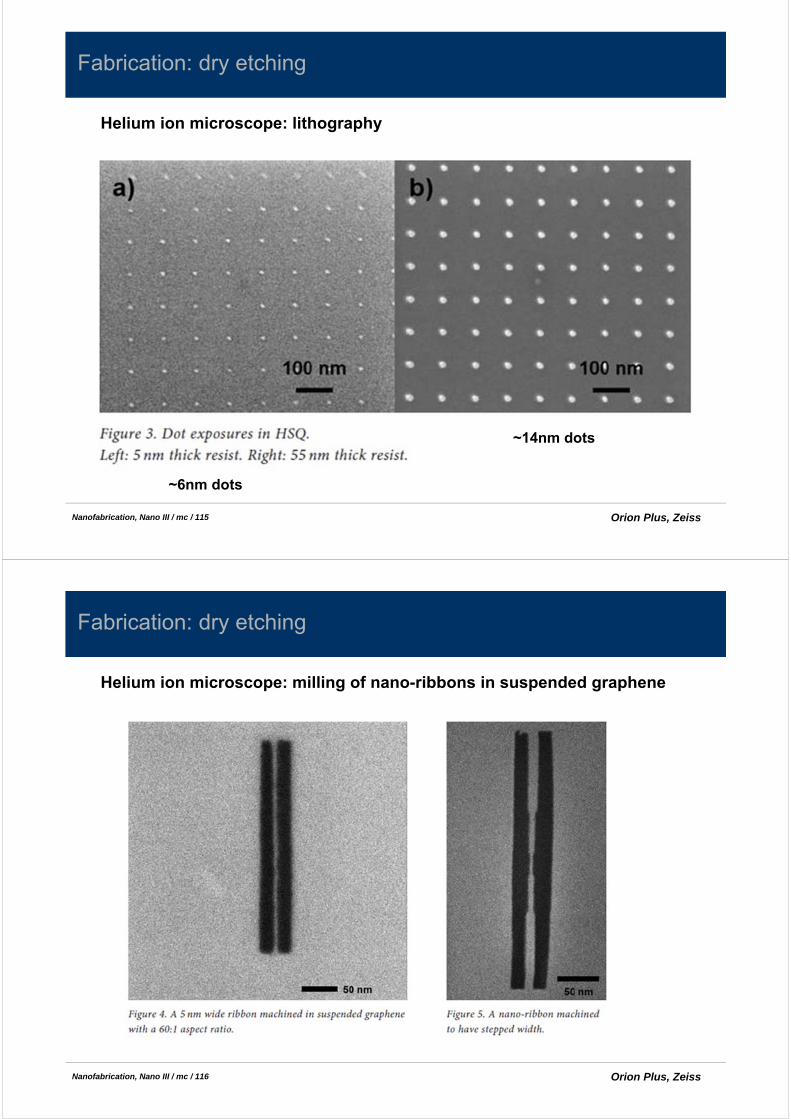
Fabrication: dry etching
Helium ion microscope: milling of nano-ribbons in suspended graphene
Orion Plus, Zeiss
Nanofabrication, Nano III / mc / 117
Outline
• Introduction:
overview, state of the art,
semiconductor physics reminder
• Fabrication basics
– IC fabrication overview
– clean-rooms
– Silicon: from powder to wafer
– material deposition techniques
– etching
– lithography
– examples of devices
silicon
silicon oxide
resist
metal
ALD oxide epoxy
80nm145nm
~10nmp-type (100) SOI
SiO2
Si handle wafer
Si
step 1.
wire length:6umwidth: 100nm-1um
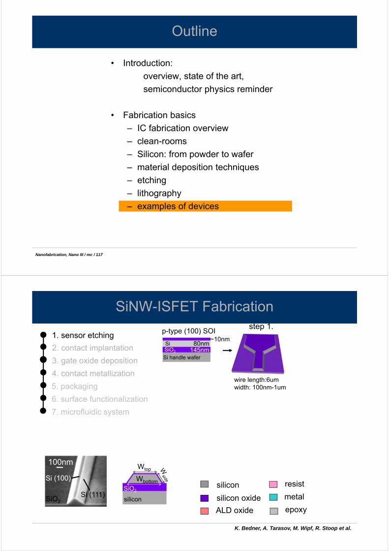
1. sensor etching
2. contact implantation
4. contact metallization
5. packaging
3. gate oxide deposition
6. surface functionalization
7. microfluidic system
Wbottom
Wtop
silicon
SiO2
100nm
Si (111)
Si (100)
SiO2
SiNW-ISFET Fabrication
K. Bedner, A. Tarasov, M. Wipf, R. Stoop et al.
silicon
silicon oxide
resist
metal
ALD oxide epoxy
80nm145nm
~10nmp-type (100) SOI
SiO2
Si handle wafer
Si
step 1.
wire length:6umwidth: 100nm-1um
PMMA
step 2.
Wbottom
Wtop
silicon
SiO2
100nm
Si (111)
Si (100)
SiO2
1. sensor etching
2. contact implantation
4. contact metallization
5. packaging
3. gate oxide deposition
6. surface functionalization
7. microfluidic system
SiNW-ISFET Fabrication
K. Bedner, A. Tarasov, M. Wipf, R. Stoop et al.
silicon
silicon oxide
resist
metal
ALD oxide epoxy
80nm145nm
~10nmp-type (100) SOI
SiO2
Si handle wafer
Si
step 1.
step 3.
wire length:6umwidth: 100nm-1um
HfO2,Al2O3
PMMA
step 2.
Wbottom
Wtop
silicon
SiO2
100nm
Si (111)
Si (100)
SiO2
1. sensor etching
2. contact implantation
4. contact metallization
5. packaging
3. gate oxide deposition
6. surface functionalization
7. microfluidic system
SiNW-ISFET Fabrication
K. Bedner, A. Tarasov, M. Wipf, R. Stoop et al.

silicon
silicon oxide
resist
metal
ALD oxide epoxy
80nm145nm
~10nmp-type (100) SOI
SiO2
Si handle wafer
Si
step 1.
step 3. step 4.
wire length:6umwidth: 100nm-1um
HfO2,Al2O3
PMMA
step 2.
Wbottom
Wtop
silicon
SiO2
100nm
Si (111)
Si (100)
SiO2
1. sensor etching
2. contact implantation
4. contact metallization
5. packaging
3. gate oxide deposition
6. surface functionalization
7. microfluidic systemmetal
SiNW-ISFET Fabrication
K. Bedner, A. Tarasov, M. Wipf, R. Stoop et al.
silicon
silicon oxide
resist
metal
ALD oxide epoxy
80nm145nm
~10nmp-type (100) SOI
SiO2
Si handle wafer
Si
step 1.
step 3. step 4. step 5.-7.
metalµ-fluidic
wire length:6umwidth: 100nm-1um
HfO2,Al2O3
receptors
PMMA
step 2.
Wbottom
Wtop
silicon
SiO2
100nm
Si (111)
Si (100)
SiO2
1. sensor etching
2. contact implantation
4. contact metallization
5. packaging
3. gate oxide deposition
6. surface functionalization
7. microfluidic system
SiNW-ISFET Fabrication
K. Bedner, A. Tarasov, M. Wipf, R. Stoop et al.

SiNW-ISFET Fabrication
48 silicon nanowires/sampletop width: 100nm – 1µm
Wbottom
Wtop
silicon
SiO2
5µm
nanowire
drain
DRAIN CONTACT
SU-8 micro-channel
28 devices
inlet
100µmmicrochannel
PDMSmicrofluidic
K. Bedner, A. Tarasov, M. Wipf, R. Stoop et al.
Nanofabrication, Nano III / mc / 124
MEMS/NEMS and devices
from MEMS (micro-electromechanical systems) …
e.g. Si gears for watch industry: lower friction and inertia
CSEM & Ulysse-Nardin
Nanofabrication, Nano III / mc / 125
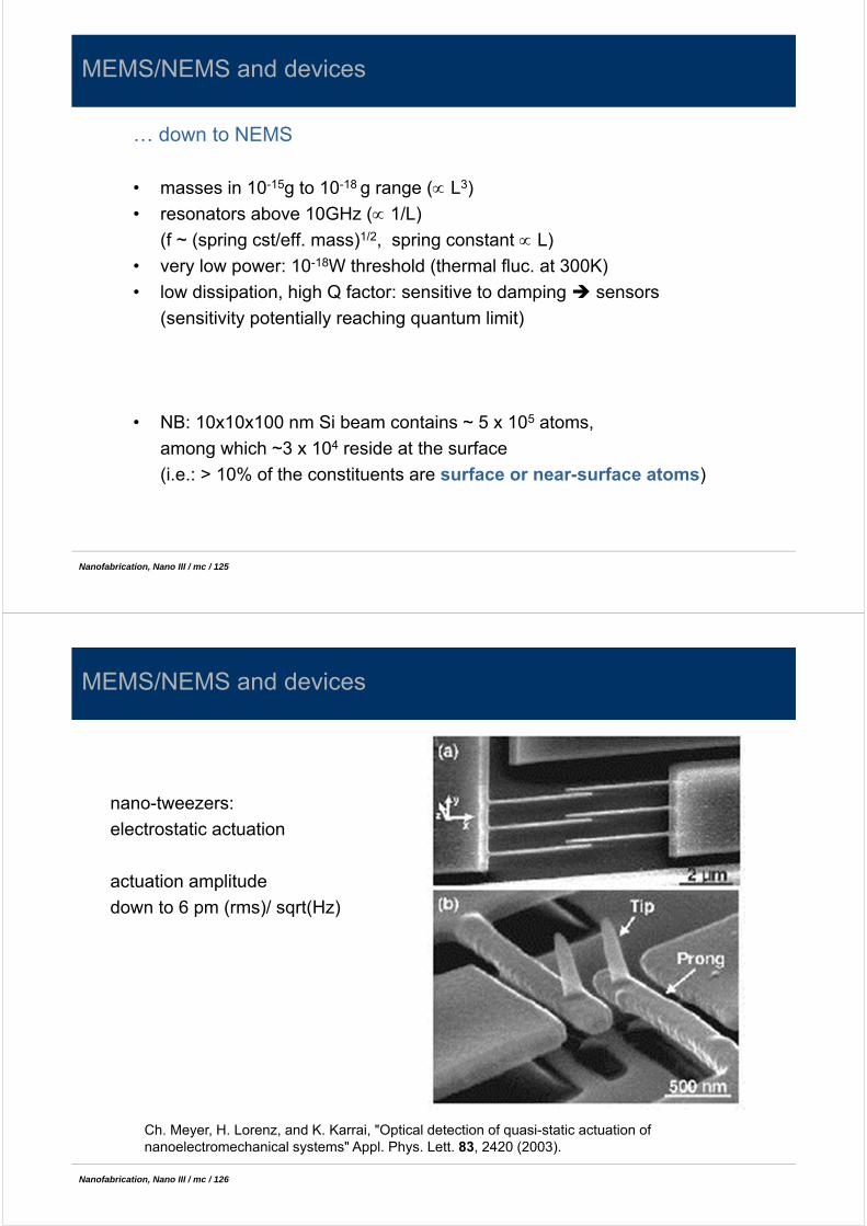
MEMS/NEMS and devices
… down to NEMS
• masses in 10-15g to 10-18 g range ( L3)
• resonators above 10GHz ( 1/L)
(f ~ (spring cst/eff. mass)1/2, spring constant L)
• very low power: 10-18W threshold (thermal fluc. at 300K)
• low dissipation, high Q factor: sensitive to damping sensors
(sensitivity potentially reaching quantum limit)
• NB: 10x10x100 nm Si beam contains ~ 5 x 10⁵ atoms,
among which ~3 x 10⁴ reside at the surface
(i.e.: > 10% of the constituents are surface or near-surface atoms)
Physics World, Feb. 2001
Nanofabrication, Nano III / mc / 126
MEMS/NEMS and devices
nano-tweezers:
electrostatic actuation
actuation amplitude
down to 6 pm (rms)/ sqrt(Hz)
Ch. Meyer, H. Lorenz, and K. Karrai, "Optical detection of quasi-static actuation of nanoelectromechanical systems" Appl. Phys. Lett. 83, 2420 (2003).

Nanofabrication, Nano III / mc / 127 Fuhrer, Zettl et al., Nature 2004
300 nm
stator (control electrodes)
rotor (metal)
axis (CNT)
MEMS/NEMS and devices
Nanofabrication, Nano III / mc / 128
Integration: hybrid devices
Tech. Roadmap for Nanoelectronics, IST program, European Commission

Nanofabrication, Nano III / mc / 129
Nanofabrication, Nano III / mc / 130
Sources and ressources
Books
• Fundamentals of Microfabrication: The Science of Miniaturization
M. Madou, 2nd ed., CRC Press, 2002
• Nanoelectronics and Information Technology
R. Waser ed., Wiley-VCH, 3rd edition, 2012
• VLSI Technology (more physical)
SM. Sze, 2nd ed., McGraw-Hill, 1988
• Introduction to Semiconductor Manufacturing Technology
H. Xiao, Prentice-Hall, 2001.