mh253 high sensitivity omni-polar hall effect switchsensors7/images/mh253_datasheet_14.pdf · mh253...
TRANSCRIPT

102010 Page 1 of 12 Rev. 1.05
MH253 High Sensitivity Omni-Polar Hall Effect Switch
MH253 Hall-effect sensor is a temperature stable, stress-resistant switch. Superior high-temperature
performance is made possible through a dynamic offset cancellation that utilizes chopper-stabilization.
This method reduces the offset voltage normally caused by device over molding, temperature
dependencies, and thermal stress.
MH253 includes the following on a single silicon chip: voltage regulator, Hall voltage generator,
small-signal amplifier, chopper stabilization, Schmitt trigger, open-drain output. Advanced CMOS wafer
fabrication processing is used to take advantage of low-voltage requirements, component matching, very
low input-offset errors, and small component geometries.
MH253 is rated for operation between the ambient temperatures –40℃ and +85℃ for the E
temperature range. The four package styles available provide magnetically optimized solutions for most
applications. Package types SO is an SOT-23(1.1 mm nominal height), SQ is an QFN2020-3(0.55 mm
nominal height), a miniature low-profile surface-mount package, while package UA is a three-lead ultra
mini SIP for through-hole mounting.
The package type is in a Halogen Free version was verified by third party Lab.
Features and Benefits
� CMOS Hall IC Technology
� Solid-State Reliability much better than reed switch
� Omni polar output switches with absolute value of North or South pole from magnet
� Low power consumption(2.6mA)
� High Sensitivity for reed switch replacement
� 100% tested at 125℃ for K.
� Small Size
� ESD HBM ±4KV Min
� COST competitive
Applications
� Solid state switch
� Lid close sensor for power supply devices
� Magnet proximity sensor for reed switch replacement in high duty cycle applications.
� Safety Key on sporting equipment
� Revolution counter
� Speed sensor
� Position Sensor
� Rotation Sensor
� Safety Key

102010 Page 2 of 12 Rev. 1.05
MH253 High Sensitivity Omni-Polar Hall Effect Switch
Ordering Information XX XXXX X XX X
αααα,ββββ,Blank…..
UA:TO-92S,VK:TO-92S(4pin),VF:TO-92S(5pin),SO:SOT-23,
SQ:QFN-3,ST:TSOT-23,SN:SOT-553,SF:SOT-89(5pin),
SS:TSOT-26,SD:DFN-6,SG:SOT-89(3pin)
E: 85O C, I: 105O C, K: 125O C, L: 150O C
181,182,185,186,187,189,281,282,248,249…
MH: Magnesensor Technology Hall Effect Product
MP: Magnesensor Technology Power ICs
Part No. Temperature Suffix Package Type MH253KUA K(-40℃to + 125℃) UA (TO-92S) MH253EUA E(-40℃to + 85℃) UA (TO-92S) MH253ESO E(-40℃to+85℃) SO (SOT-23) MH253ESQ E(-40℃to+85℃) SQ (QFN2020-3)
Custom sensitivity selection is available by MST sorting technology
Functional Diagram
Note: Static sensitive device; please observe ESD precautions. Reverse VDD protection is not included. For reverse voltage
protection, a 100Ω resistor in series with VDD is recommended.
Company Name
Part Number
Temperature Code
Package Type
Sorting Code

102010 Page 3 of 12 Rev. 1.05
MH253 High Sensitivity Omni-Polar Hall Effect Switch
C1:10nF
C2:100pF
R1:10KΩ
Absolute Maximum Ratings (Tz=+25˚C)
Characteristics Values Unit
Supply voltage,(VDD) 7 V
Output Voltage,(Vout) 6 V
Reverse voltage, (VDD) (VOUT) -0.3 V
Magnetic flux density Unlimited Gauss
Output current,(IOUT) 25 mA
Operating Temperature Range, (Ta) “E” version -40 to +85 ℃
“K” version -40 to +125 ℃
Storage temperature range, (Ts) -55 to +150 ℃
Maximum Junction Temp,(Tj) 150 ℃
Thermal Resistance (θJA) UA / SO / SQ 206 / 543 / 543 ℃/W
(θJC) UA / SO / SQ 148 / 410 /410 ℃/W
Package Power Dissipation, (PD) UA / SO / SQ 606 / 230 / 230 mW
Note: Exceeding the absolute maximum ratings may cause permanent damage to the device. Exposure to absolute
Maximum-rated conditions for extended periods may affect device reliability.
Electrical Specifications
DC Operating Parameters TA=+25℃, VDD=5.0V
Parameters Test Conditions Min Typ Max Units
Supply Voltage,(VDD) Operating 2.5 6 V
Supply Current,(IDD) Average 2.6 6.0 mA
Output Low Voltage,(VDSON) IOUT=10mA 400 mV
Output Leakage Current,(Ioff) IOFF B<BRP, VOUT = 5V 10 uA
Output Rise Time,(TR) RL=10kΩ, CL =20pF 0.45 uS
Output Fall Time,(TF) RL=10kΩ; CL =20pF 0.45 uS
Electro-Static Discharge HBM 4 KV
Typical Application circuit
102010 Page 4 of 12 Rev. 1.05
MH253 High Sensitivity Omni-Polar Hall Effect Switch
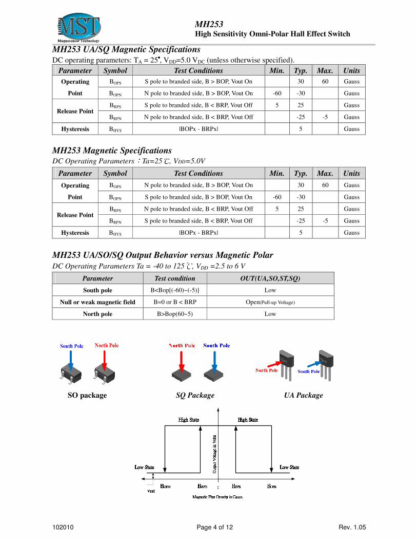
MH253 UA/SQ Magnetic Specifications
DC operating parameters: TA = 25°°°°, VDD=5.0 VDC (unless otherwise specified).
Parameter Symbol Test Conditions Min. Typ. Max. Units
Operating
Point
BOPS S pole to branded side, B > BOP, Vout On 30 60 Gauss
BOPN N pole to branded side, B > BOP, Vout On -60 -30 Gauss
Release Point BRPS S pole to branded side, B < BRP, Vout Off 5 25 Gauss
BRPN N pole to branded side, B < BRP, Vout Off -25 -5 Gauss
Hysteresis BHYS |BOPx - BRPx| 5 Gauss
MH253 Magnetic Specifications DC Operating Parameters:Ta=25℃, VDD=5.0V
Parameter Symbol Test Conditions Min. Typ. Max. Units
Operating
Point
BOPS N pole to branded side, B > BOP, Vout On 30 60 Gauss
BOPN S pole to branded side, B > BOP, Vout On -60 -30 Gauss
Release Point BRPS N pole to branded side, B < BRP, Vout Off 5 25 Gauss
BRPN S pole to branded side, B < BRP, Vout Off -25 -5 Gauss
Hysteresis BHYS |BOPx - BRPx| 5 Gauss
MH253 UA/SO/SQ Output Behavior versus Magnetic Polar
DC Operating Parameters Ta = -40 to 125℃, VDD =2.5 to 6 V
Parameter Test condition OUT(UA,SO,ST,SQ)
South pole B<Bop[(-60)~(-5)] Low
Null or weak magnetic field B=0 or B < BRP Open(Pull-up Voltage)
North pole B>Bop(60~5) Low
SO package SQ Package UA Package
VsatVsatVsatVsat BBBBOPNOPNOPNOPN BBBBRPNRPNRPNRPN BBBBRPSRPSRPSRPS BBBBOPSOPSOPSOPSHigh StateHigh StateHigh StateHigh State
Low StateLow StateLow StateLow State Low StateLow StateLow StateLow StateOOOOuuuuttttppppuuuutttt VVVVoooollllttttaaaaggggeeee iiiinnnn VVVVoooollllttttssssMagnetic Flux Density in GaussMagnetic Flux Density in GaussMagnetic Flux Density in GaussMagnetic Flux Density in Gauss0High StateHigh StateHigh StateHigh State

102010 Page 5 of 12 Rev. 1.05
MH253 High Sensitivity Omni-Polar Hall Effect Switch
Performance Graphs
Typical Supply Voltage(VDD) Versus Flux Density
Typical Temperature(TA) Versus Flux Density
Typical Temperature(TA) Versus Supply Current(IDD)
Typical Supply Voltage(VDD) Versus Supply Current(IDD)
Typical Supply Voltage(VDD) Versus Output Voltage(VDSON)
Typical Temperature(TA) Versus Output Voltage(VDSON)
-60.0
-40.0
-20.0
0.0
20.0
40.0
60.0
2.5 3 3.5 4 4.5 5 5.5 6
Flu
x D
ensi
ty(G
au
ss)
Supply Voltage(V)
BOPS
BRPS
BOPN
BRPN
25℃-60.0
-40.0
-20.0
0.0
20.0
40.0
60.0
-40 -20 0 25 55 85 100 125
Flu
x D
ensi
ty(G
au
ss)
Temperature(℃℃℃℃)
BOPS
BRPS
BOPN
BRPN
5V
0.0
1.0
2.0
3.0
4.0
5.0
6.0
7.0
8.0
9.0
10.0
-40 -20 0 25 55 85 100 125
Cu
rren
t C
on
sum
pio
n(m
A)
Temperature(℃℃℃℃)
5V
0.0
1.0
2.0
3.0
4.0
5.0
6.0
7.0
8.0
9.0
10.0
2.5 3 3.5 4 4.5 5 5.5 6
Cu
rren
t C
on
sum
pio
n(m
A)
Supply Voltage(V)
25℃
0.0
50.0
100.0
150.0
200.0
250.0
300.0
350.0
400.0
2.5 3 3.5 4 4.5 5 5.5 6
Ou
tpu
t S
atu
rati
on
Volt
ag
e (m
V)
Supply Voltage(V)
25℃@10mA
0.0
50.0
100.0
150.0
200.0
250.0
300.0
350.0
400.0
-40 -20 0 25 55 85 100 125
Ou
tpu
t S
atu
rati
on
Vo
lta
ge
(mV
)
Temperature(℃℃℃℃)
5V@10mA

102010 Page 6 of 12 Rev. 1.05
MH253 High Sensitivity Omni-Polar Hall Effect Switch
Typical Supply Voltage(VDD) Versus Leakage Current(IOFF)
Power Dissipation versus Temperature(TA)
Package Power Dissipation The power dissipation of the Package is a function of the pad size. This can vary from the minimum
pad size for soldering to a pad size given for maximum power dissipation. Power dissipation for a surface
mount device is determined by TJ(max), the maximum rated junction temperature of the die, RθJA, the
thermal resistance from the device junction to ambient, and the operating temperature, Ta. Using the
values provided on the data sheet for the package, PD can be calculated as follows:
a j
J(max)
DR
Ta-TP
θ
=
The values for the equation are found in the maximum ratings table on the data sheet. Substituting
these values into the equation for an ambient temperature Ta of 25°C, one can calculate the power
dissipation of the device which in this case is 606 milliwatts.
606mWC/206
C25-C150(UA)P
W
D =°
°°=
The 206℃/W for the UA package assumes the use of the recommended footprint on a glass epoxy
printed circuit board to achieve a power dissipation of 606 milliwatts. There are other alternatives to
achieving higher power dissipation from the Package. Another alternative would be to use a ceramic
substrate or an aluminum core board such as Thermal Clad. Using a board material such as Thermal Clad,
an aluminum core board, the power dissipation can be doubled using the same footprint.
0.000
0.010
0.020
0.030
0.040
0.050
2.5 3 3.5 4 4.5 5 5.5 6
Ou
tpu
t L
eak
age
Cu
rren
t(u
A)
Supply Voltage(V)
25℃0100200300400500600700
-40 0 40 80 120Pa
ckag
e p
ow
er D
issi
pa
tio
n(m
W)
Temperature(℃℃℃℃)
UA PackageUA PackageUA PackageUA PackageRRRRθja = 206= 206= 206= 206℃℃℃℃/w/w/w/wSO/SQ PackageSO/SQ PackageSO/SQ PackageSO/SQ PackageRRRRθja = 543= 543= 543= 543℃℃℃℃/w/w/w/w

102010 Page 7 of 12 Rev. 1.05
MH253 High Sensitivity Omni-Polar Hall Effect Switch
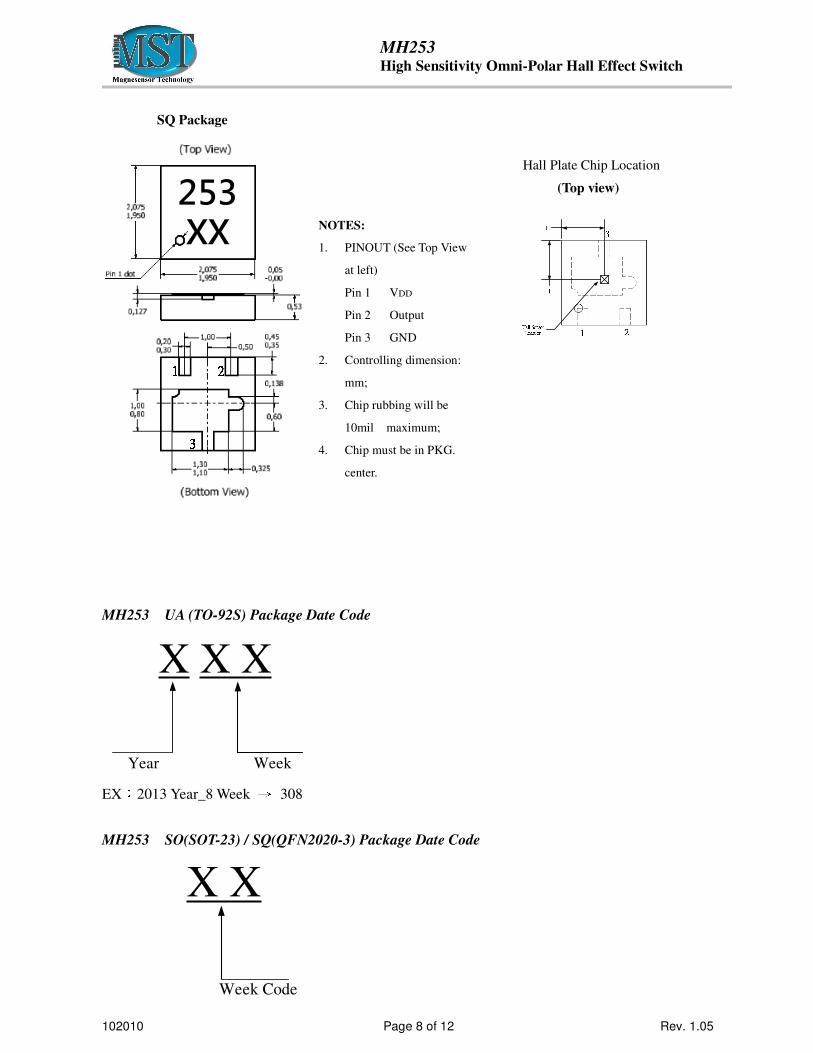
Sensor Location, package dimension and marking
MH251 Package
UA Package Hall Chip Location
253XXX
SO Package Hall Plate Chip Location
(Top View) (Bottom view)
253XX1111 22223333
NOTES:
1).Controlling dimension: mm
2).Leads must be free of flash
and plating voids
3).Do not bend leads within 1
mm of lead to package
interface.
4).PINOUT:
Pin 1 VDD
Pin 2 GND
Pin 3 Output
Output Pin Assignment
(Top view)
NOTES:
1. PINOUT (See Top View at left :)
Pin 1 VDD
Pin 2 Output
Pin 3 GND
2. Controlling dimension: mm
3. Lead thickness after solder plating
will be 0.254mm maximum
102010 Page 8 of 12 Rev. 1.05
MH253 High Sensitivity Omni-Polar Hall Effect Switch
SQ Package
253XX
1111 22223333
MH253 UA (TO-92S) Package Date Code
X X X
Year Week
EX:2013 Year_8 Week → 308
MH253 SO(SOT-23) / SQ(QFN2020-3) Package Date Code
X X
Week Code
Hall Plate Chip Location
(Top view)
NOTES:
1. PINOUT (See Top View
at left)
Pin 1 VDD
Pin 2 Output
Pin 3 GND
2. Controlling dimension:
mm;
3. Chip rubbing will be
10mil maximum;
4. Chip must be in PKG.
center.
102010 Page 9 of 12 Rev. 1.05
MH253 High Sensitivity Omni-Polar Hall Effect Switch
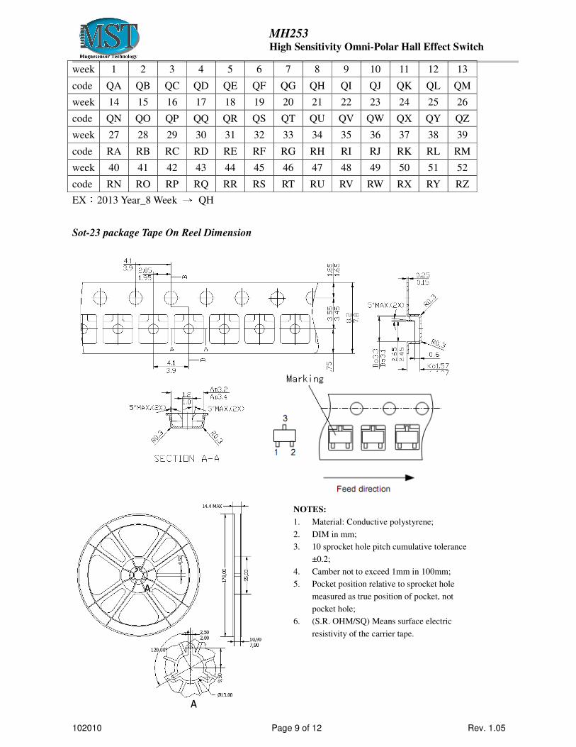
week 1 2 3 4 5 6 7 8 9 10 11 12 13
code QA QB QC QD QE QF QG QH QI QJ QK QL QM
week 14 15 16 17 18 19 20 21 22 23 24 25 26
code QN QO QP QQ QR QS QT QU QV QW QX QY QZ
week 27 28 29 30 31 32 33 34 35 36 37 38 39
code RA RB RC RD RE RF RG RH RI RJ RK RL RM
week 40 41 42 43 44 45 46 47 48 49 50 51 52
code RN RO RP RQ RR RS RT RU RV RW RX RY RZ
EX:2013 Year_8 Week → QH
Sot-23 package Tape On Reel Dimension
NOTES:
1. Material: Conductive polystyrene;
2. DIM in mm;
3. 10 sprocket hole pitch cumulative tolerance
±0.2;
4. Camber not to exceed 1mm in 100mm;
5. Pocket position relative to sprocket hole
measured as true position of pocket, not
pocket hole;
6. (S.R. OHM/SQ) Means surface electric
resistivity of the carrier tape.

102010 Page 10 of 12 Rev. 1.05
MH253 High Sensitivity Omni-Polar Hall Effect Switch
QFN2020-3 Tape On Reel Dimension
IR reflow curve
NOTES:
1. Material: Conductive polystyrene;
2. DIM in mm;
3. 10 sprocket hole pitch cumulative
tolerance ±0.2;
4. Camber not to exceed 1mm in 100mm;
5. Pocket position relative to sprocket
hole measured as true position of
pocket, not pocket hole;
6. (S.R. OHM/SQ) Means surface
electric resistivity of the carrier tape.
102010 Page 11 of 12 Rev. 1.05
MH253 High Sensitivity Omni-Polar Hall Effect Switch
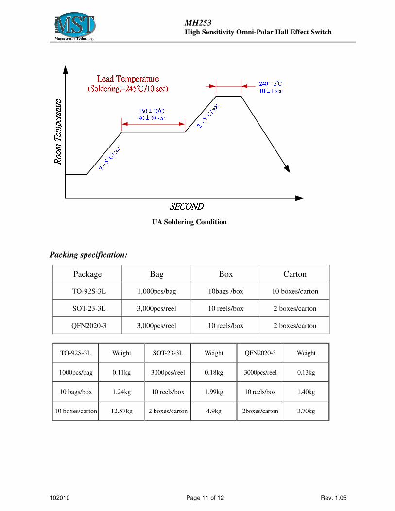
UA Soldering Condition
Packing specification:
Package Bag Box Carton
TO-92S-3L 1,000pcs/bag 10bags /box 10 boxes/carton
SOT-23-3L 3,000pcs/reel 10 reels/box 2 boxes/carton
QFN2020-3 3,000pcs/reel 10 reels/box 2 boxes/carton
TO-92S-3L Weight SOT-23-3L Weight QFN2020-3 Weight
1000pcs/bag 0.11kg 3000pcs/reel 0.18kg 3000pcs/reel 0.13kg
10 bags/box 1.24kg 10 reels/box 1.99kg 10 reels/box 1.40kg
10 boxes/carton 12.57kg 2 boxes/carton 4.9kg 2boxes/carton 3.70kg

102010 Page 12 of 12 Rev. 1.05
MH253 High Sensitivity Omni-Polar Hall Effect Switch
Inner box label::::Size: 3.4cm*6.4cm Bag and inner box Halogen Free Label
Carton label::::Size: 5.6 cm * 9.8 cm Bag and inner box Halogen Free Label
Combined lots:
When combing lots, one reel could have two D/C and no more than two DC. One carton could have
two devices, no more than two.