081511 mh249 datasheet v101 -...
TRANSCRIPT

081511 Page 1 of 12 Rev. 1.01
MH 249 High Sensitivity Omni-Polar Hall Effect Switch
MH 249 Hall-effect sensor is a temperature stable, stress-resistant switch. Superior high-temperature performance is made possible through a dynamic offset cancellation that utilizes chopper-stabilization. This method reduces the offset voltage normally caused by device over molding, temperature dependencies, and thermal stress.
MH 249 includes the following on a single silicon chip: voltage regulator, Hall voltage
generator, small-signal amplifier, chopper stabilization, Schmitt trigger, and a short circuit protected open-drain output. Advanced CMOS wafer fabrication processing is used to take advantage of low-voltage requirements, component matching, very low input-offset errors, and small component geometries.
MH 249 is rated for operation between the ambient temperatures –40°C and +85°C for the
E temperature range. The four package styles available provide magnetically optimized solutions for most applications. Package types SO is an SOT-23(1.1 mm nominal height), SQ is an QFN2020-3(0.55 mm nominal height), a miniature low-profile surface-mount package, while package UA is a three-lead ultra mini SIP for through-hole mounting.
The package type is in a Green version was verified by third party Lab.
Features and Benefits CMOS Hall IC Technology
Solid-State Reliability much better than reed switch
Omni polar output switches with absolute value of North or South pole from magnet
Operation down to 1.8 V and Max at 6V.
High Sensitivity for reed switch replacement
Small Size
ESD HBM +/-4KV Min
COST competitive
Applications Solid state switch
Lid close sensor for power supply devices
Magnet proximity sensor for reed switch replacement in high duty cycle applications.
Safety Key on sporting equipment
Revolution counter
Speed sensor
Position Sensor
Rotation Sensor
Safety Key
081511 Page 2 of 12 Rev. 1.01
MH 249 High Sensitivity Omni-Polar Hall Effect Switch
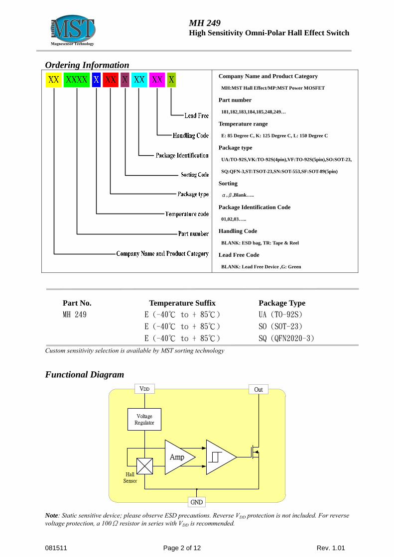
Ordering Information
Part No. Temperature Suffix Package Type
MH 249 E (-40℃ to + 85℃) UA (TO-92S)
E (-40℃ to + 85℃) SO (SOT-23)
E (-40℃ to + 85℃) SQ (QFN2020-3)
Custom sensitivity selection is available by MST sorting technology
Functional Diagram
VoltageRegulator
Amp
VDD
GND
Hall Sensor
Out
Note: Static sensitive device; please observe ESD precautions. Reverse VDD protection is not included. For reverse voltage protection, a 100Ω resistor in series with VDD is recommended.
Company Name and Product Category
MH:MST Hall Effect/MP:MST Power MOSFET
Part number
181,182,183,184,185,248,249…
Temperature range
E: 85 Degree C, K: 125 Degree C, L: 150 Degree C
Package type
UA:TO-92S,VK:TO-92S(4pin),VF:TO-92S(5pin),SO:SOT-23,
SQ:QFN-3,ST:TSOT-23,SN:SOT-553,SF:SOT-89(5pin)
Sorting
α,β,Blank…..
Package Identification Code
01,02,03…..
Handling Code
BLANK: ESD bag, TR: Tape & Reel
Lead Free Code
BLANK: Lead Free Device ,G: Green

081511 Page 3 of 12 Rev. 1.01
MH 249 High Sensitivity Omni-Polar Hall Effect Switch
C1:10nF
C2:100pF
R1:5KΩ
Absolute Maximum Ratings At (Ta=25°C)
Characteristics Values Unit
Supply voltage,(VDD) 6 V
Out voltage, (VOUT) 6 V
Reverse voltage, (VDD) (VOUT) -0.3 V
Magnetic flux density Unlimited Gauss
Output current,(IOUT) 25 mA
Operating temperature range, (Ta) -40 to +85 °C
Storage temperature range, (Ts) -55 to +150 °C
Maximum Junction Temp,(Tj) 150 °C
Thermal Resistance (θJA) UA / SO / SQ 206 / 543 / 543 °C / W
(θJC) UA / SO / SQ 148 / 410 /410 °C / W
Package Power Dissipation, (PD) UA / SO / SQ 606 / 230 / 230 mW
Electro-Static Discharge,(HMB) 4 KV
Note: Exceeding the absolute maximum ratings may cause permanent damage. Exposure to absolute maximum-
rated conditions for extended periods may affect device reliability.
Electrical Specifications DC Operating Parameters Ta=25°C, VDD=1.8V (Unless otherwise specified)
Parameters Test Conditions Min Typ Max Units
Supply Voltage,(VDD) Operating 1.8 6 Volts
Supply Current,(IDD) Average 1.5 mA
Output Current,(IOUT) 10 mA
Output Low Voltage,(VSAT) IOUT=1mA 200 mV
Output Leakage Current,(Ioff) IOFF B<BRP, VOUT = 6V 10 uA
Output Rise Time,( TR) VDD = 6V, RL=1kΩ, CL =20pF 0.45 uS
Output Fall Time,( TF) RL=1kΩ, CL =20pF 0.45 uS
Typical Application circuit
OutC1
MH182MH249
Vcc
R1
C2
VDD
Out
GND
081511 Page 4 of 12 Rev. 1.01
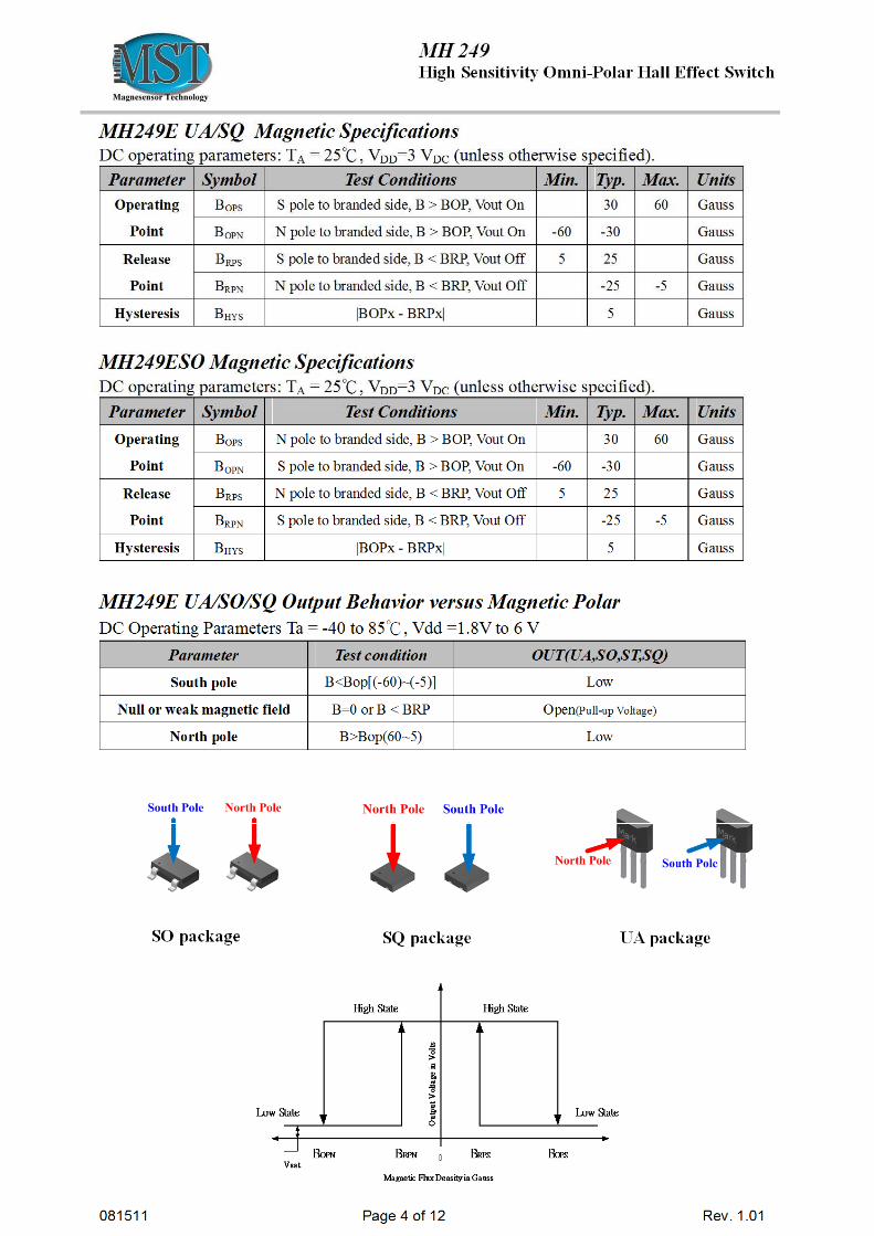
MH 249 High Sensitivity Omni-Polar Hall Effect Switch
SO package UA package
081511 Page 5 of 12 Rev. 1.01
MH 249 High Sensitivity Omni-Polar Hall Effect Switch
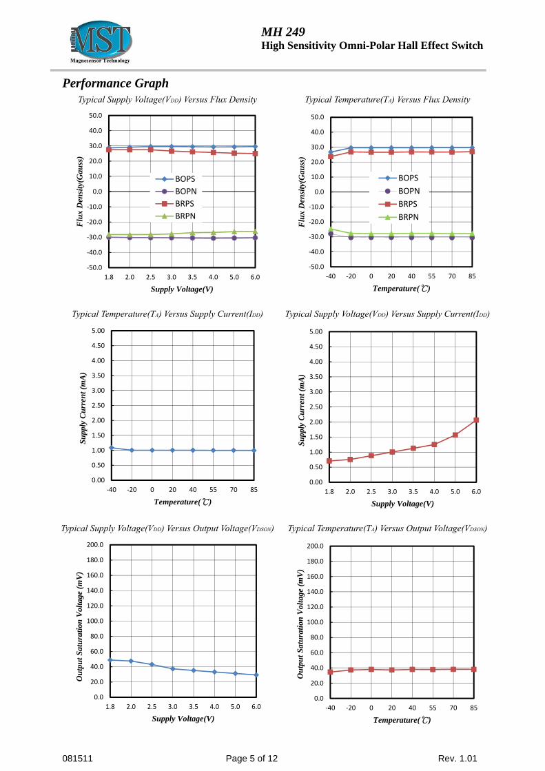
Performance Graph Typical Supply Voltage(VDD) Versus Flux Density
Typical Temperature(TA) Versus Flux Density
Typical Temperature(TA) Versus Supply Current(IDD)
Typical Supply Voltage(VDD) Versus Supply Current(IDD)
Typical Supply Voltage(VDD) Versus Output Voltage(VDSON)
Typical Temperature(TA) Versus Output Voltage(VDSON)
‐50.0
‐40.0
‐30.0
‐20.0
‐10.0
0.0
10.0
20.0
30.0
40.0
50.0
1.8 2.0 2.5 3.0 3.5 4.0 5.0 6.0
Flu
x D
ensi
ty(G
auss
)
Supply Voltage(V)
BOPS
BOPN
BRPS
BRPN
‐50.0
‐40.0
‐30.0
‐20.0
‐10.0
0.0
10.0
20.0
30.0
40.0
50.0
‐40 ‐20 0 20 40 55 70 85
Flu
x D
ensi
ty(G
auss
)
Temperature(℃)
BOPS
BOPN
BRPS
BRPN
0.00
0.50
1.00
1.50
2.00
2.50
3.00
3.50
4.00
4.50
5.00
‐40 ‐20 0 20 40 55 70 85
Su
pply
Cu
rren
t (m
A)
Temperature(℃)
0.00
0.50
1.00
1.50
2.00
2.50
3.00
3.50
4.00
4.50
5.00
1.8 2.0 2.5 3.0 3.5 4.0 5.0 6.0
Su
pply
Cu
rren
t (m
A)
Supply Voltage(V)
0.0
20.0
40.0
60.0
80.0
100.0
120.0
140.0
160.0
180.0
200.0
1.8 2.0 2.5 3.0 3.5 4.0 5.0 6.0
Ou
tpu
t Sat
ura
tion
Vol
tage
(m
V)
Supply Voltage(V)
0.0
20.0
40.0
60.0
80.0
100.0
120.0
140.0
160.0
180.0
200.0
‐40 ‐20 0 20 40 55 70 85
Ou
tpu
t Sat
ura
tion
Vol
tage
(m
V)
Temperature(℃)
081511 Page 6 of 12 Rev. 1.01
MH 249 High Sensitivity Omni-Polar Hall Effect Switch
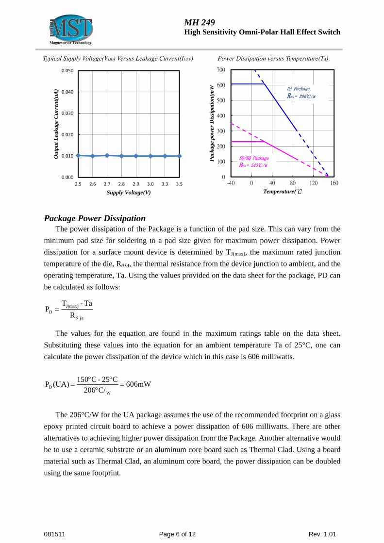
Typical Supply Voltage(VDD) Versus Leakage Current(IOFF)
Power Dissipation versus Temperature(TA)
Package Power Dissipation The power dissipation of the Package is a function of the pad size. This can vary from the
minimum pad size for soldering to a pad size given for maximum power dissipation. Power
dissipation for a surface mount device is determined by TJ(max), the maximum rated junction
temperature of the die, RθJA, the thermal resistance from the device junction to ambient, and the
operating temperature, Ta. Using the values provided on the data sheet for the package, PD can
be calculated as follows:
a j
J(max)D R
Ta-TP
The values for the equation are found in the maximum ratings table on the data sheet.
Substituting these values into the equation for an ambient temperature Ta of 25°C, one can
calculate the power dissipation of the device which in this case is 606 milliwatts.
606mWC/206
C25-C150(UA)P
WD
The 206°C/W for the UA package assumes the use of the recommended footprint on a glass
epoxy printed circuit board to achieve a power dissipation of 606 milliwatts. There are other
alternatives to achieving higher power dissipation from the Package. Another alternative would
be to use a ceramic substrate or an aluminum core board such as Thermal Clad. Using a board
material such as Thermal Clad, an aluminum core board, the power dissipation can be doubled
using the same footprint.
0.000
0.010
0.020
0.030
0.040
0.050
2.5 2.6 2.7 2.8 2.9 3.0 3.3 3.5
Ou
tpu
t Lea
kage
Cu
rren
t(u
A)
Supply Voltage(V)
0
100
200
300
400
500
600
700
-40 0 40 80 120 160
Pac
kage
pow
er D
issi
pati
on(m
W
Temperature(℃
UA Package
Rθja= 206℃/w
SO/SQ Package
Rθja= 543℃/w
081511 Page 7 of 12 Rev. 1.01
MH 249 High Sensitivity Omni-Polar Hall Effect Switch
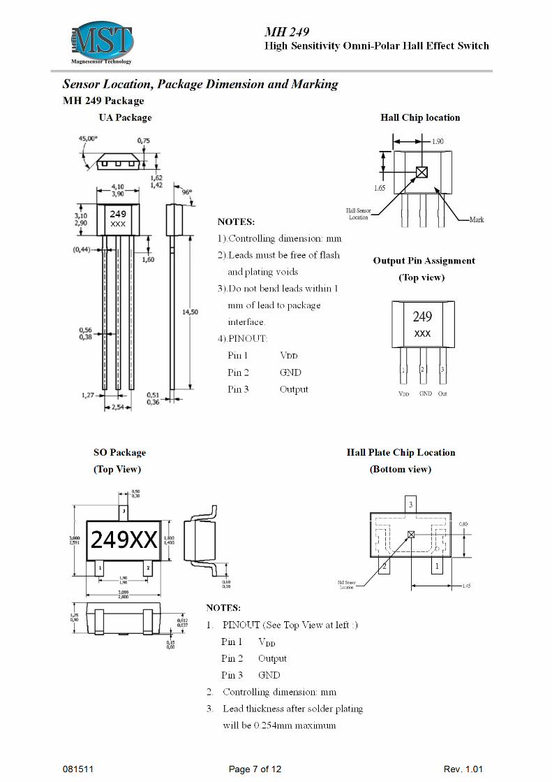
Sensor Location, Package Dimension and Marking MH 249 Package
UA Package Hall Chip location
249XXX
SO Package Hall Plate Chip Location
(Top View) (Bottom view)
249XX1 2
3
NOTES:
1).Controlling dimension: mm
2).Leads must be free of flash
and plating voids
3).Do not bend leads within 1
mm of lead to package
interface.
4).PINOUT:
Pin 1 VDD
Pin 2 GND
Pin 3 Output
081511 Page 8 of 12 Rev. 1.01
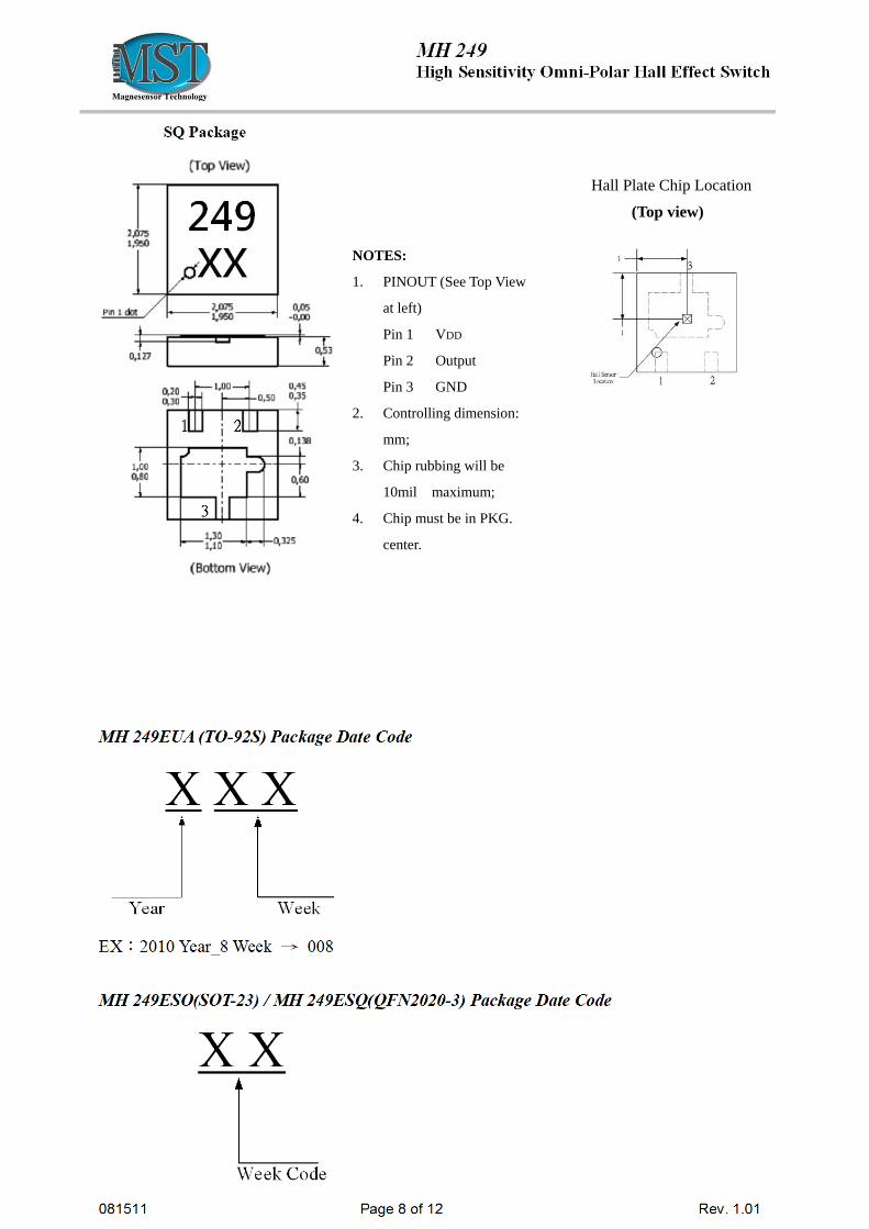
Hall Plate Chip Location
(Top view)
NOTES:
1. PINOUT (See Top View
at left)
Pin 1 VDD
Pin 2 Output
Pin 3 GND
2. Controlling dimension:
mm;
3. Chip rubbing will be
10mil maximum;
4. Chip must be in PKG.
center.
081511 Page 9 of 12 Rev. 1.01
MH 249 High Sensitivity Omni-Polar Hall Effect Switch
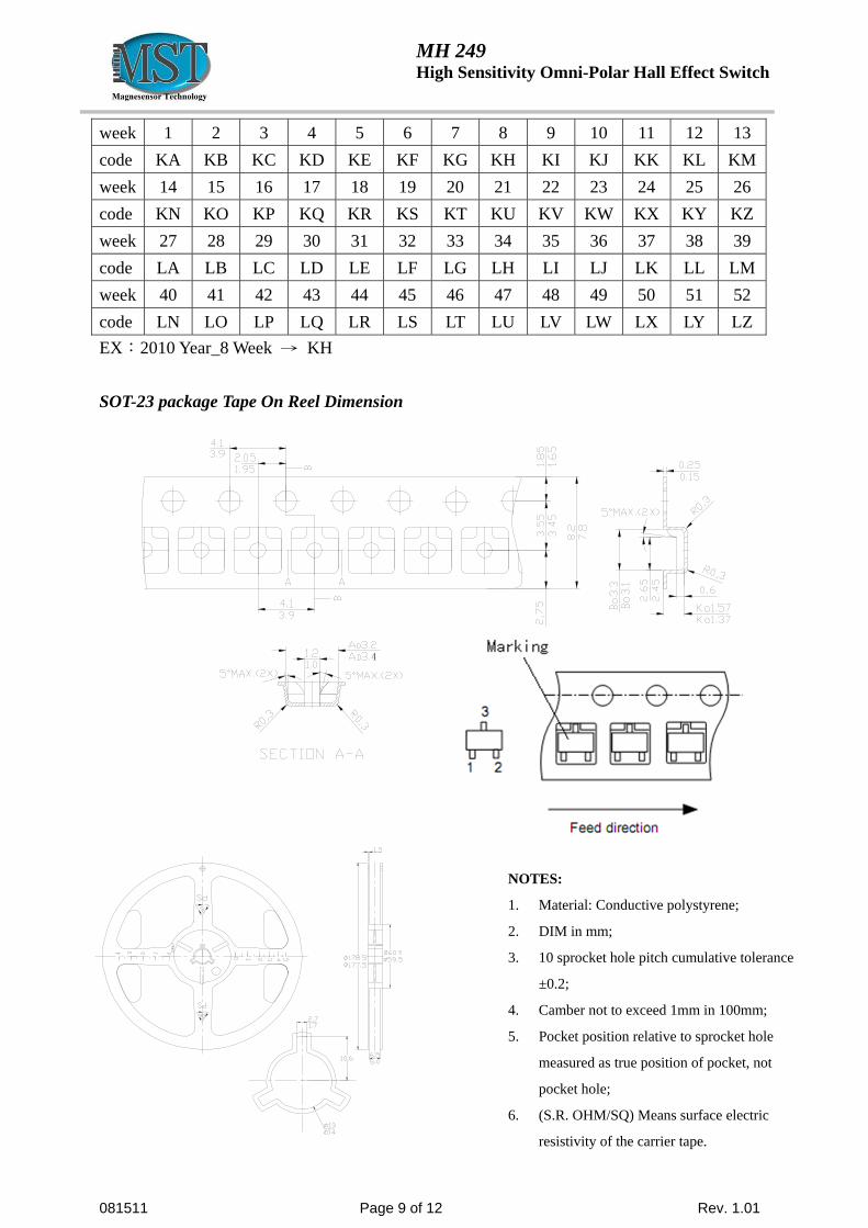
week 1 2 3 4 5 6 7 8 9 10 11 12 13
code KA KB KC KD KE KF KG KH KI KJ KK KL KM
week 14 15 16 17 18 19 20 21 22 23 24 25 26
code KN KO KP KQ KR KS KT KU KV KW KX KY KZ
week 27 28 29 30 31 32 33 34 35 36 37 38 39
code LA LB LC LD LE LF LG LH LI LJ LK LL LM
week 40 41 42 43 44 45 46 47 48 49 50 51 52
code LN LO LP LQ LR LS LT LU LV LW LX LY LZ
EX:2010 Year_8 Week → KH
SOT-23 package Tape On Reel Dimension
4
NOTES:
1. Material: Conductive polystyrene;
2. DIM in mm;
3. 10 sprocket hole pitch cumulative tolerance
±0.2;
4. Camber not to exceed 1mm in 100mm;
5. Pocket position relative to sprocket hole
measured as true position of pocket, not
pocket hole;
6. (S.R. OHM/SQ) Means surface electric
resistivity of the carrier tape.
081511 Page 10 of 12 Rev. 1.01
MH 249 High Sensitivity Omni-Polar Hall Effect Switch
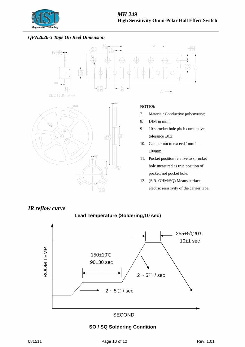
QFN2020-3 Tape On Reel Dimension
IR reflow curve
Lead Temperature (Soldering,10 sec)
SO / SQ Soldering Condition
RO
OM
TE
MP
2 ~ 5℃ / sec
2 ~ 5℃ / sec
2 ~ 5℃ / sec
150±10℃
90±30 sec
255+5℃/0℃
10±1 sec
SECOND
NOTES:
7. Material: Conductive polystyrene;
8. DIM in mm;
9. 10 sprocket hole pitch cumulative
tolerance ±0.2;
10. Camber not to exceed 1mm in
100mm;
11. Pocket position relative to sprocket
hole measured as true position of
pocket, not pocket hole;
12. (S.R. OHM/SQ) Means surface
electric resistivity of the carrier tape.
081511 Page 11 of 12 Rev. 1.01
MH 249 High Sensitivity Omni-Polar Hall Effect Switch
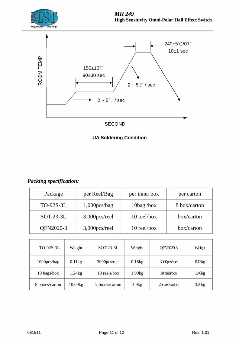
UA Soldering Condition
Packing specification:
Package per Reel/Bag per inner box per carton
TO-92S-3L 1,000pcs/bag 10bag /box 8 box/carton
SOT-23-3L 3,000pcs/reel 10 reel/box box/carton
QFN2020-3 3,000pcs/reel 10 reel/box box/carton
TO-92S-3L Weight SOT-23-3L Weight QFN2020-3 Weight
1000pcs/bag 0.11kg 3000pcs/reel 0.18kg 3000pcs/reel 0.13kg
10 bags/box 1.24kg 10 reels/box 1.99kg 10 reels/box 1.40kg
8 boxes/carton 10.09kg 2 boxes/carton 4.9kg 2boxes/carton 3.70kg
RO
OM
TE
MP
2 ~ 5℃ / sec
2 ~ 5℃ / sec
2 ~ 5℃ / sec
150±10℃
90±30 sec
240+5℃/0℃
10±1 sec
SECOND
081511 Page 12 of 12 Rev. 1.01
MH 249 High Sensitivity Omni-Polar Hall Effect Switch
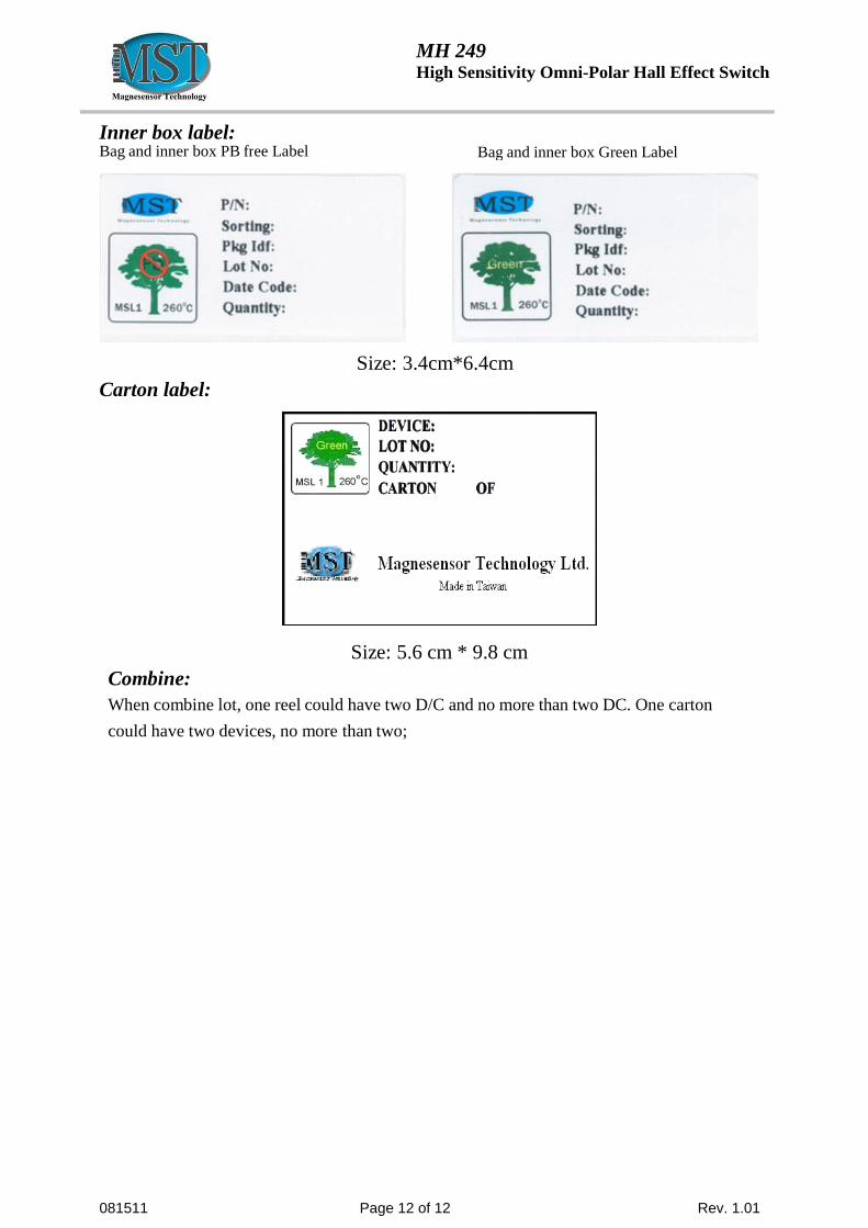
Inner box label: Bag and inner box PB free Label Bag and inner box Green Label
Size: 3.4cm*6.4cm Carton label:
Size: 5.6 cm * 9.8 cm Combine: When combine lot, one reel could have two D/C and no more than two DC. One carton
could have two devices, no more than two;