metal gate electrode impurity engineering for control of ... roll off – electrical thickness...
TRANSCRIPT

Metal Gate Electrode Impurity Engineering for Control of Effective Work Function
Jim Chambers, Hiro Niimi, Andrei Li-Fatou and Judy ShawTexas Instruments, Incorporated, Advanced CMOS
Chris Hinkle, Jim Burris, Husam Alshareef, Richard Chapman, Rohit Galatage and Eric VogelUniversity of Texas at Dallas, Department of Materials Science and Engineering
Mikael Christensen, Clive Freeman and Erich WimmerMaterials Design, Incorporated
February 23, 2010

2
Outline
• Introduction– High-k gate dielectrics– Metal gate electrodes– This work
• Oxygen impurities in CVD W– High work function– WF, EOT and mobility degradation
• Post-Metal Annealing for Metal Gate Impurity Control– Experimental– Oxygen incorporation into TiN– Effective work function of PMA oxygen annealed PVD TiN
• Ab initio simulation of TiN/HfO2 gate stacks– TiN/HfO2 interface formation– Effect of interface dipole on work function– Thermodynamics of vacancy filling– Model for metal gate work function engineering
• Summary

3
Today’s Performance versus Power Tradeoff
Standby Power (a.u.)
Rel
ativ
e P
erfo
rman
ce (a
.u.) Servers
PCCell
Station
Netbook
SmartPhone
MobileMultimedia
Medicalrf
CellPhone
~3 O
rder
s
~6 Orders

4
Approach to Reducing Standby Power Today
• CMOS power reduction strategies– Reduce supply voltage
P = CV2f– Reduce subthreshold leakage
Jss ~ exp(1/Vt)– Reduce gate induced drain
leakageGIDL ~ Defects
– Reduce gate leakageJg ~ exp(thickness)
High-k Gate DielectricsMetal Gate Electrodes
Today

5
Advanced CMOS Cross-Section
• SiON tunneling current limits scaling
Interconnect Level
Contact Level
Gate Level
Gate Dielectric Level
Polysilicon
c-Si
SiON
9Å
Cu
W Plug
Polysilicon

6
Motivation for High-k Gate DielectricsHigh-k gate dielectrics reduce gate leakage
SiO2
Si Substrate
GateElectrode
High-k
Si Substrate
GateElectrode
↑Dielectric constant↑Thickness
Challenge Replacing Mother Nature’s nearly perfect SiO2 dielectric
HK
SiOHKPhysThkEOT
εε
2=
1. SiO2
2. High-k
1.E-05
1.E-04
1.E-03
1.E-02
1.E-01
1.E+00
1.E+01
1.E+02
1.E+03
0.0 10.0 20.0 30.0Equivalent Oxide Thickness (Å)
Gat
e Le
akag
e (A
/cm
2 )
30% SiO240% SiO260% SiO270% SiO280% SiO2SiO2 Trend
↑ %HfO2
↑ %N or ↓ Thk
1
2

7
Motivation for Metal Gate ElectrodesMetal gates eliminate gate depletion and increase capacitanceMetal gates provide gate leakage scaling
Challenge Obtaining correct metal gate work functions
1.E-051.E-041.E-031.E-021.E-011.E+001.E+011.E+021.E+031.E+04
5 10 15 20 25 30Inversion Electrical Thickness (Å)
Gat
e Le
akag
e (A
/cm
2 )
↓Depletion
0
50
100
150
200
250
300
-1.0 -0.5 0.0 0.5 1.0 1.5 2.0
Gate Voltage (V)
Gat
e C
apac
itanc
e (p
F)
Metal GateNpoly = 2E20 cm-3Npoly = 1E20 cm-3Npoly = 5E19 cm-3
EOT = 1.0nm
↓Depletion
High-k
Si Substrate
P+
PolysiliconElectrode
Depletion Layer
High-k
Si Substrate
P+
PolysiliconElectrode
Depletion Layer
High-k
Si Substrate
MetalGate
Electrode
High-k
Si Substrate
MetalGate
Electrode
1. Poly Gate
2. Metal Gate
1
2
12
SiO2 Trend Line

8
• What is the source of large variation in reported eWFs?Impurities in metal electrode / high-k gate stacks
ΔWF ~ 600meV
Summary reported by Mizubayashi, VLSI, 42, 2008
Motivation for This WorkLarge variation observed in reported work functions

9
Outline
• Introduction– High-k gate dielectrics– Metal gate electrodes– This work
• Oxygen impurities in CVD W– High work function– WF, EOT and mobility degradation
• Post-Metal Annealing for Metal Gate Impurity Control– Experimental– Oxygen incorporation into TiN– Effective work function of PMA oxygen annealed PVD TiN
• Ab initio simulation of TiN/HfO2 gate stacks– TiN/HfO2 interface formation– Effect of interface dipole on work function– Thermodynamics of vacancy filling– Model for metal gate work function engineering
• Summary

10
Dual Work Function Metal Gate Integration
• Dual work function metal gate– Required for optimized device performance
• High thermal budget, gate-first integration approach– Material system W-WSi2 pair– WSi2 formed from the PMOS metal by reaction– Enables dual metal integration without exposing dielectric to metal etch
• Target Work Function– NMOS = 4.15 eV Si conduction band edge– PMOS = 5.1 eV Si valence band edge
Si
Poly-Si
Gate DielectricW
Barrier
NiSi
Poly-Si
Gate DielectricWSi2
Barrier
NiSi
NiSi NiSiNiSi
PMOS NMOS

11
DWFMG Roadblock WF, EOT and Mobility Entitlement
• W electrodes Scaling the electrical thickness results in Vfb roll off– Electrical thickness degradation– Mobility degradation
-1.0
-0.5
0.0
0.5
1.0
1.5
0 2 4 6 8 10EOT (nm)
Flat
Ban
d V
olta
ge (V
)
PMOS Vfb Roll Off
W WF = 4.97 eV
WSi2 WF = 4.37 eV
Vfb Roll Off
0.0
1.0
2.0
3.0
4.0
5.0
6.0
7.0
-2.0 -1.0 0.0 1.0 2.0Voltage (V)
Cap
acita
nce
(pF)
MG EOT DegradationTiN
W
0
100
200
300
400
500
600
Effective Field (MV/cm)
Mob
ility
(cm
2 /V-s
)
0.2 0.6 1.0 1.4
MG Mobility Degradation
TiN
W
Universal Mobility
W/HfSiON

12
• As deposited W contains high level of oxygen impurity
– W(CO)6 precursor• Clustered N2 anneal reduces oxygen impurity
SIMS – Impact of Clustering
1.E+18
1.E+19
1.E+20
1.E+21
1.E+22
1.E+23
0 200 400 600 800 1000 1200Depth (A)
[O] (
cm-3
)
Clustered No Anneal
Clustered + 800C N2
TaN W SiO2
TaN
W
SiO2
AnnealClustered
Oxygen Impurity Observed in CVD W
W(CO)6
CO
W
As Dep

13
Model Describing WF/EOT/Mobility Degradation Due to O-Impurities in W
High-k Directly on SiHigh-k Directly on SiHigh-k on Thick SiO2High-k on Thick SiO2
OO O
OO
OO
OO
VV
VV
VV
V
OOO
OO
OO
O OV
VV
VO
O
OO O O OX
OO O
OO
OO
OO
VV
VV
VV
V
TaN
W
HK
SiO2
c-Si
TaN
W
HK
SiO2
c-Si
Oxygen impurityin CVD W
As Deposited
Gate First Thermal
Oxygen vacancyin high-k
Oxygen migrationto interfaceOxygen fills
vacancy in HK
Thick SiO2Diffusion barrier
As Deposited
Gate First ThermalTaN
W
HKSiO2c-Si
TaN
W
HK
c-Si
Oxygen impurityin CVD W
Oxygen vacancyin high-k
OOOO
VV
V
VO
V
V O
Low oxygenat interface
Low vacancy filling in HK
Interfacial SiO2growth

14
Outline
• Introduction– High-k gate dielectrics– Metal gate electrodes– This work
• Oxygen impurities in CVD W– High work function– WF, EOT and mobility degradation
• Post-Metal Annealing for Metal Gate Impurity Control– Experimental– Oxygen incorporation into TiN– Effective work function of PMA oxygen annealed PVD TiN
• Ab initio simulation of TiN/HfO2 gate stacks– TiN/HfO2 interface formation– Effect of interface dipole on work function– Thermodynamics of vacancy filling– Model for metal gate work function engineering
• Summary

15
Ideal Replacement Metal Gate and High-k Device Structure
• Low thermal budget, gate-last integration approach• TiN as metal gate on both NMOS and PMOS• WF engineering on NMOS side to decrease work function• WF engineering on PMOS side to increase work function
Si
Metal Fill
HfSiONTiN
Metal Fill
HfSiONNiSi NiSiNiSi
PMOS NMOS
TiN
Challenge Can oxygen be used for WF engineering to increase the work function for PMOS?

16
Experimental• Goal
– Understand the role of oxygen impurities in HK/MG stacks in determining the effective work function
• Gate stacks– ALD HfO2 gate dielectric– PVD TiN gate electrode
• Annealing– RTP 10-100s– 450-1000 °C– P = 200 Torr– Ambient
• N2 with residual oxygen contamination (university tool)• 10% O2/N2
• Physical analysis– SIMS (Dynamic and Cation)– XRD
• Electrical analysis– MOSCAP– CV @ 100kHz NCSU CVC

17
Depth (nm)0 20 40 60 80 100
[O] (
#/cm
3 )
1e+17
1e+18
1e+19
1e+20
1e+21
1e+22
1e+23
1e+24400C, 10s 400C, 30s 450C, 20s 500C, 10s 500C, 30s
Depth (nm)0 5 10 15 20
[O] (
#/cm
3 )
1e+21
1e+22
1e+23400C, 10s 400C, 30s 450C, 20s 500C, 10s 500C, 30s
Controlled Oxygen Incorporation into TiN
• 400 °C No appreciable oxygen incorporation
• 450C-500 °C Controllable oxygen addition
O2400-500 °C10-30s
O2400-500 °C10-30s
↓ Thermal Budget
TiN Si
TargetMGthickness
50nm TiN
c-Si
O2 Anneal
SiO2

18
Method to Determine Interface Composition
• Si-capped sandwich TiN stacks Determine impact of anneal only• Oxygen-free in-situ TiN/a-Si interface• Interfaces defined at 50% rise/fall of Si signal
Depth (nm)0 20 40 60 80 100
Con
cent
ratio
n (#
/cm
3 )
1e+20
1e+21
1e+22
1e+23
a-Si a-Si
TiN
“Top”Interface
OSi
10nm TiN
a-Si
40nm a-Si
In-situ
10nm TiN
a-Si
40nm a-Si
In-situ
C-SIMS

19
Equivalent Oxide Thickness (nm)0 1 2 3
Flat
band
Vol
tage
(V)
-0.5
0.0
0.5
1.0
[O] = 2.1E20 cm-3
[O] = 6.0E21 cm-3
[O] = 1.3E22 cm-3
[O] = 2.1E20 cm-3
[O] = 6.0E21 cm-3
[O] = 1.3E22 cm-3sm φφ −
Wor
k Fu
nctio
n +5
50m
eV
↑[O]
Depth (nm)0 10 20 30 40 50
[O] (
cm-3
)
1020
1021
1022
1023
[O] = 2.1E20 cm-3
[O] = 6.0E21 cm-3
[O] = 1.3E22 cm-3
[O] = 2.1E20 cm-3
[O] = 6.0E21 cm-3
[O] = 1.3E22 cm-3
a-Si TiN a-Si
WF Increased by Engineered Oxygen Incorporation
Post-TiN anneal optimized for oxygen
incorporation at interface
High-k
100Å TiN
SiO2
n-Si
High-k
100Å TiN
SiO2
n-Si
4000Å Al
Anneal
10nm TiN
a-Si
Anneal
40nm a-Si
Work function increased by 550meV by engineered oxygen
incorporation

20
2Theta20 25 30 35 40 45 50
Inte
nsity
(a.u
.)
As Deposited450C, N2, 30s450C, 10% O2/N2, 30s500C, N2, 30s500C, 10% O2/N2, 30s
TiN<111>
TiN<200>
Anatase<101>
TiN Phase Maintained for 450 °C Anneals
• No phase change observed from as deposited to 450 °C anneals and 500 °C, N2
• TiN annealed at 500 °C, 10% O2/N2, 30s almost entirely converted to TiO2
As
Dep
osite
d
“N2”
, 450
C, 3
0s
10%
O2/N
245
0C, 3
0s
As
Dep
“N2”
500C
30s
10%
O2/N
250
0C, 3
0s
a-Si
TiNa-Si

21
Outline
• Introduction– High-k gate dielectrics– Metal gate electrodes– This work
• Oxygen impurities in CVD W– High work function– WF, EOT and mobility degradation
• Post-Metal Annealing for Metal Gate Impurity Control– Experimental– Oxygen incorporation into TiN– Effective work function of PMA oxygen annealed PVD TiN
• Ab initio simulation of TiN/HfO2 gate stacks– TiN/HfO2 interface formation– Effect of interface dipole on work function– Thermodynamics of vacancy filling– Model for metal gate work function engineering
• Summary

22
Computational Methodology
• First-principles calculations– VASP (Vienna Ab initio Simulation Package)– Density functional theory (DFT) with Perdew, Burke and Ernzerhof (PBE)
generalized gradient approximation (GGA)– All-electron frozen core approach with projector augmented wave (PAW) method– Structures
• Crystallographic literature• Simulated annealing• Energy minimization
– Properties• System energies• Partial densities of states• Electrostatic potentials
• Modeling infrastructure– MedeA for model and interface construction, calculation management and analysis
TiN
HfO2
23
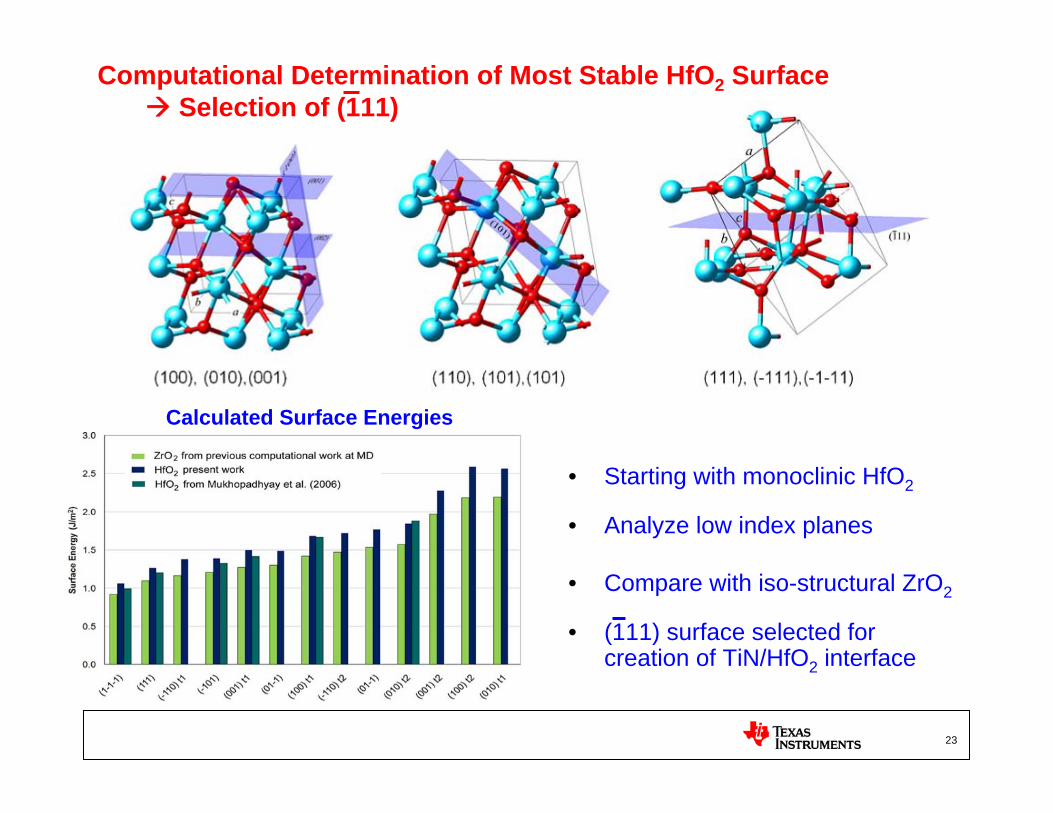
Computational Determination of Most Stable HfO2 Surface Selection of (111)
• Starting with monoclinic HfO2
• Analyze low index planes
• Compare with iso-structural ZrO2
• (111) surface selected for creation of TiN/HfO2 interface
Calculated Surface Energies

24
Relaxed HfO2 (111) Surface
• Surface structure– Two types of oxygen with coordination of 3– Bridging oxygen– Hafnium with 4 and 5 fold coordination
• Bulk contains Hf coordinated with 7 oxygen atoms
Side View Perspective View

25
TiN/HfO2 Interface Structure after Simulated Annealing and Energy Minimization
• TiN rock salt (111) + HfO2 monoclinic (111)• Systematic search for lattice match• Match at lattice shift of 4° and 2.8% area• 288 atoms per supercell
Top View
Cross-Section
Abrupt TiN/HfO2interface
26
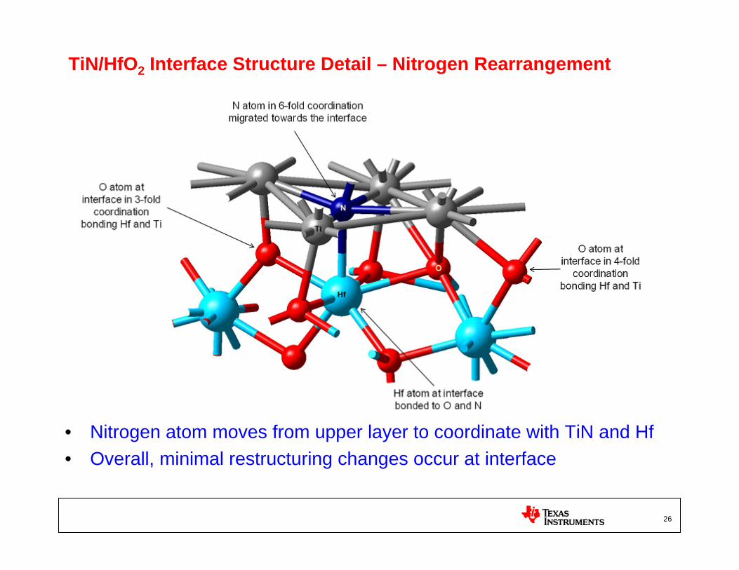
TiN/HfO2 Interface Structure Detail – Nitrogen Rearrangement
• Nitrogen atom moves from upper layer to coordinate with TiN and Hf• Overall, minimal restructuring changes occur at interface

27
Electrostatic Potential of TiN/HfO2 Stack
• Planar average exhibits ripples associated with each atomic layer• Macroscopic average taken as the moving average across several layers• Macroscopic average used as basis for comparison between test cases

28
Ab Initio Modeling Confirms Increase in Work Function with Presence of N-induced Dipole
• Dipole due to oxygen in TiN screened due to metal atoms• N-induced dipole at interface can not be screened by the dielectric• Additional simulations indicate > 400 meV shift for N replacing all O at interface
N replacing O at interface
O replacing Ninside TiN
~0 meV
HfO2 TiN HfO2 TiN

29
Ab Initio Modeling Confirms Decrease in Work Functionfor Oxygen Vacancy at Interface
• Oxygen vacancies decrease work function• Conversely, filling oxygen vacancies increases work function
3030
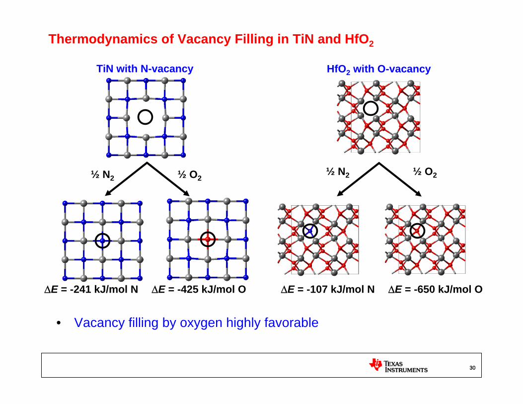
Thermodynamics of Vacancy Filling in TiN and HfO2
• Vacancy filling by oxygen highly favorable
½ N2
ΔE = -241 kJ/mol N ΔE = -425 kJ/mol O ΔE = -107 kJ/mol N ΔE = -650 kJ/mol O
TiN with N-vacancy HfO2 with O-vacancy
½ O2 ½ N2 ½ O2

31
TiN
HfO2c-Si
V V VV
NXX
Thermodynamics of N-induced Dipole Formation
• Not favorable for N from TiN to fill HfO2 O-vacancy• Combination of TiN oxygenation + O-vacancy filling by N is favorable
Oxygen vacancy
TiN
HfO2c-Si
ΔE = 134 kJ/mol N ΔE = -425 kJ/mol O ΔE = -291 kJ/mol N
V V VV
½ O2
N
V V VV
½ O2
V
Nitrogen vacancy
32
Depth (nm)0 10 20 30 40 50 60
Con
cent
ratio
n (#
/cm
3 )
1e+16
1e+17
1e+18
1e+19
1e+20
1e+21
1e+22
1e+23
1e+24
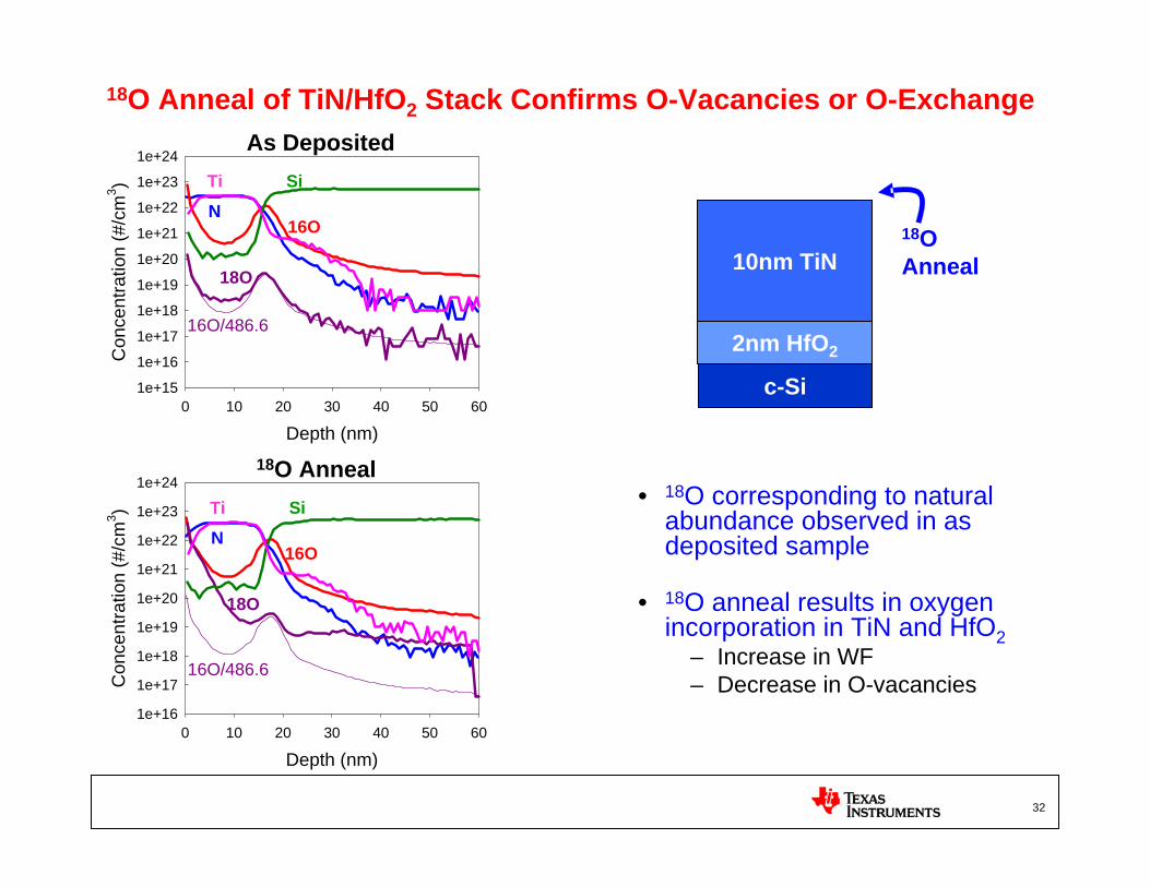
18O Anneal of TiN/HfO2 Stack Confirms O-Vacancies or O-Exchange
• 18O corresponding to natural abundance observed in as deposited sample
• 18O anneal results in oxygen incorporation in TiN and HfO2
– Increase in WF– Decrease in O-vacancies
Depth (nm)0 10 20 30 40 50 60
Con
cent
ratio
n (#
/cm
3 )
1e+15
1e+16
1e+17
1e+18
1e+19
1e+20
1e+21
1e+22
1e+23
1e+24
18OAnneal
c-Si
2nm HfO2
10nm TiN
TiN
Si
16O
18O
16O/486.6
TiN
Si
16O
18O
16O/486.6
As Deposited
18O Anneal

33
Model Describing Mechanism for WF Increase due to Low Temp O2 PMA
TiN
HfO2c-Si
V
V
½ O2
N
V
½ O2
TiN
HfO2c-Si
V
V V
N-vacancy in TiN
O-vacancy in HfO2
Low Temp O2 Anneal
TiON
HfO2c-Si
O
N
O
O
Oxygenated TiN
N at InterfaceFilled O-vacancy
As Deposited
During Anneal
Post-Anneal
½ O

3434
Ongoing Work Includes a Complete Gate Stack Model
Si SiO2 HfO2 TiN Al
1.7nm 1.5nm 1.4nm 1.2nm

35
Summary
• Ab initio simulation used to guide and confirm experiment
• Simulations indicate the effective work function can be engineered by controlling dipoles at the HK/MG interface and in the HK
• Oxygen incorporation by low temperature anneal of TiN/HK gate stacks resultings in a N-induced dipole that can increase the effective work function by 550 meV