measurement of the optical dielectric function of transition ... 1! measurement of the optical...
TRANSCRIPT
1
Measurement of the optical dielectric function of transition metal dichalcogenide monolayers: MoS2, MoSe2, WS2 and WSe2
Yilei Li1, Alexey Chernikov1, Xian Zhang2, Albert Rigosi1, Heather M. Hill1, Arend M. van der Zande2,3, Daniel A. Chenet2, En-Min Shih1, James Hone2, Tony F. Heinz1*
1Departments of Physics and Electrical Engineering, Columbia University, 538 West 120th St., New York, NY 10027, USA
2Department of Mechanical Engineering, Columbia University, 500 West 120th Street, New York, NY 10027, USA
3Energy Frontier Research Center, Columbia University, 500 West 120th Street, New York, NY 10027, USA
* To whom correspondence should be addressed: [email protected]
Abstract: We report a determination of the complex in-plane dielectric function of monolayers of
four transition metal dichalcogenides: MoS2, MoSe2, WS2 and WSe2, for photon energies from
1.5 – 3 eV. The results were obtained from reflection spectra using a Kramers-Kronig
constrained variational analysis. From the dielectric functions, we obtain the absolute absorbance
of the monolayers. We also provide a comparison of the dielectric function for the monolayers
with the corresponding bulk materials.
2
I. INTRODUCTION
Transition metal dichalcogenide (TMDC) crystals have emerged as a new class of
semiconductors that display distinctive properties at monolayer thickness [1-3]. Their optical
properties are of particular interest and importance. They exhibit a transition to direct band gap
semiconductors at monolayer thickness [4,5], offer access to the valley degree of freedom by
optical helicity [6-9], and display strong excitonic properties, with tightly bound neutral and
charged excitons, as well as a non-hydrogenic Rydberg series of excited states [10-17]. The
materials thus provide an excellent testing ground for the physics of 2D systems and many-body
effects in solids. At the same time, they have attracted much interest for applications in
optoelectronics as light emitters, detectors, and photovoltaic devices [18-25].
The most basic description of light-matter interactions in TMDC monolayers is given by
the materials’ complex dielectric function. The dielectric function provides a meeting point
between experiment and theories of excited-state properties of this novel class of materials;
knowledge of the dielectric function is also crucial for the characterization of these materials and
for their use in emerging applications. Despite its central role, a systematic study of the optical
dielectric functions for these materials has yet to be reported.
In this paper, we present a determination of the complex in-plane dielectric functions of
four monolayer TMDCs – MoS2, MoSe2, WS2, and WSe2 – for the photon energies between 1.5
and 3 eV. Our study complements earlier ellipsometry measurements on monolayer MoS2 [26-
28]. We obtain the dielectric functions by Kramers-Kronig constrained analysis of the
reflectance spectra of the monolayer samples supported on a transparent substrate. We also
present calculated absorption spectra for the four different monolayers. The strong light-matter
interaction leads to peaks in the imaginary part of the dielectric function for the A exciton
3
exceeding 30 in some of the materials, with a corresponding single-layer absorption exceeding
15%. For the purpose of further understanding the resonance features in the dielectric response,
we extract transition energies of resonances peaks and analyze several trends in the material
response, including comparisons with previously reported bulk dielectric functions.
II. OPTICAL REFLECTANCE MEASUREMENT
We prepared the relevant monolayer TMDC samples on fused silica substrates by
mechanical exfoliation of bulk crystals (2Dsemiconductors Inc.) [29] For comparison, we also
examined selected monolayers prepared by chemical vapor deposition [30-34]. Samples of
monolayer thickness were first identified by their optical contrast under a microscope with
additional verification of thickness by Raman and photoluminescence spectroscopy.
The dielectric function was determined by reflectance measurements of the samples at
room temperature. The reflectance measurements were performed using broadband emission
from a tungsten halogen lamp, which was spatially filtered by a pinhole before being focused
onto the sample using an objective. The spot size on sample was about 2 µm. The reflected light
was collected by the same objective and deflected by a beam splitter to a spectrometer equipped
with a CCD camera cooled to liquid-nitrogen temperature. We determined the reflectance spectra
of the samples by normalizing the measured reflected power by that from the bare fused silica
substrate. The reflectance from the fused silica substrate was calibrated using literature values for
the material’s refractive index [35]. The spectral resolution of our measurements was 2 meV,
which was much narrower than any feature in the spectra. In our experimental configuration, the
optical fields lie in the plane of the sample, thus only the in-plane dielectric response is accessed.
4
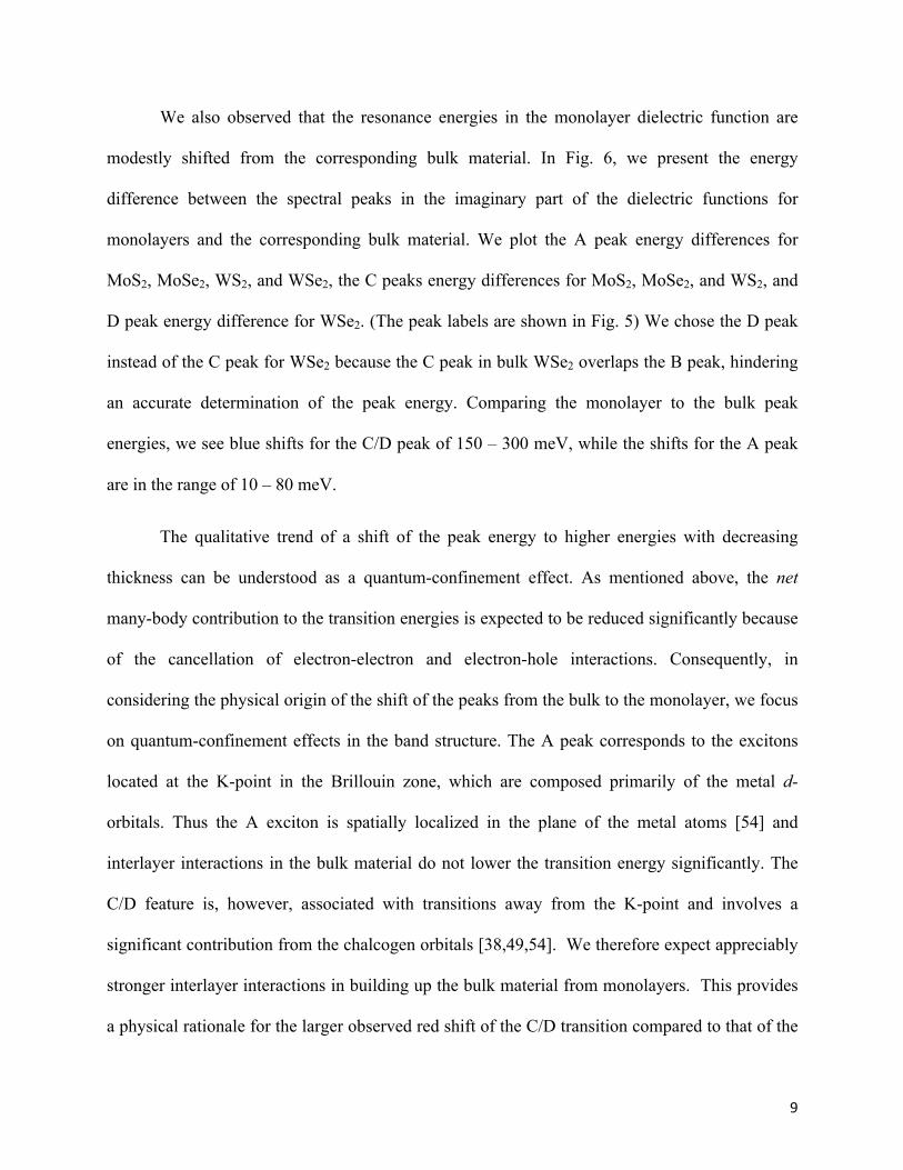
The absolute reflectance spectra for the TMDC monolayers on fused silica are presented
in Figs. 1(a-d). For all four TMDC monolayers, the two lowest energy peaks in the reflectance
spectra correspond to the excitonic features associated with interband transitions at the K (K’)
point in the Brillouin zone [36]. The two features, denoted by A and B, are attributed to the
splitting of the valence band by spin-orbit coupling [37]. At higher photon energies we observe
the spectrally broad response from higher-lying interband transitions [36], including the
transitions near the Γ point [38,39].
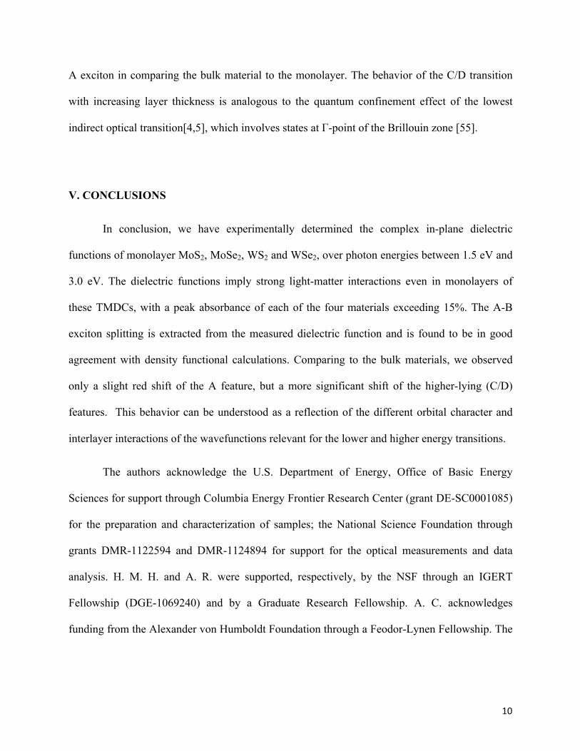
The dielectric functions derived in this paper are obtained from exfoliated TMDC
monolayer flakes. Different samples of the same material generally exhibit very similar optical
response. This is illustrated by a comparison of the reflectance spectra for two different
exfoliated samples of MoS2 in Fig. 2(a). Charge doping, strain, and inhomogeneity can cause
slight changes in the position and line widths of the narrow excitonic peaks in the spectral
response. These differences are more apparent in comparisons with samples grown by chemical
vapor deposition (CVD). Fig. 2(b) shows a comparison of the reflectance spectra for exfoliated
and CVD-grown MoS2 monolayers. Shifts in the A and B peaks of ~ 40 meV are observed,
although the overall dielectric function is very similar.
III. DETERMINATION OF THE COMPLEX DIELECTRIC FUNCTION BY
KRAMERS-KRONIG CONSTRAINED ANALYSIS
We obtain the dielectric function 𝜀 𝐸 for the four different TMDC monolayers from the
experimental reflectance spectra by a Kramers-Kronig constrained analysis. We analyze the
reflectance data treating the monolayer as a homogeneous medium with an effective thickness
given by the interlayer spacing of the respective bulk material [36] (dMoS2= 6.15 Å, dMoSe2= 6.46
5
Å, dWS2= 6.18 Å, and dWSe2= 6.49 Å). The optical reflectance is calculated by the standard thin-
film analysis [40], which fully accounts for all interference effects.
We model the complex dielectric function 𝜀 𝐸 = 𝜀% 𝐸 + 𝑖𝜀( 𝐸 of the samples as a
function of photon energy E using a superposition of Lorentzian oscillators:
𝜀 𝐸 = 1 + *+,+-.,-./,0+
123% . (1)
Here 𝑓2 and 𝛾2 are the oscillator strength and the line width of the k-th oscillator, and 𝐸2 runs
over the full spectral range. In our treatment, we choose a uniform spacing between the
oscillators of 2 meV, much smaller than the narrowest feature in the optical spectra, and a full
width of the individual oscillators of 10 meV to yield a spectrally smooth response. Note that the
narrow width of the individual oscillators are only used for the modeling of an arbitrary
dielectric function, and should not be associated with the lifetime of the electronic transitions.
Satisfaction of the Kramers-Kronig relation is built into the functional form of Eq. (1) and does
not need to be considered separately [41]. We fit the measured reflectance data using the
dielectric function of Eq. (1), varying the oscillator strengths 𝑓2 between 1.5 eV and 3 eV are
varied to match the experimental data.
Our reflectance measurements only cover the spectral range of 1.5 eV ≤ E ≤ 3 eV.
Within our Kramers-Kronig constrained analysis, optical transitions outside this energy range
need to be considered for an accurate determination of 𝜀. We consider first the behavior at lower
photon energies. In the infrared, the dielectric response arises from polar phonons and free
carriers. Based on the weakness of the contribution of polar phonons in bulk materials [42,43] to
the visible dielectric response, we can neglect this term. The influence of free carriers on the
dielectric functions in the optical frequency range is estimated to be less than 0.1, using the
6
Drude model for a carrier density of 1012 cm-2, chosen on the basis of transport characteristics of
usual TMDC transistor devices [4,44]. We therefore also neglect this contribution.
The influence of higher-energy electronic transitions, however, needs to be taken into
account. Strong electronic transitions lie just beyond our measurement window. To address this
issue, we make use of data for the bulk materials [45,46], including transitions up to a photon
energy of E = 30 eV. As discussed below, the monolayer and bulk dielectric functions are quite
similar at higher energies. We therefore expect the bulk dielectric function to provide an
adequate approximation of the dielectric function to correct for the off-resonant response of
higher-lying transitions.
With respect to experimental technique for the determination of the dielectric function,
we note that rather than applying the Kramers-Kronig constrained analysis of the reflectance
data, one could consider measurement of both reflection and transmission spectra of the sample.
In principle, this yields two independent measurements for each photon energy, thus directly
determining 𝜀% and 𝜀(, without recourse to the Kramers-Kronig analysis. For a thin layer on a
transparent substrate, as is the case here, however, both the transmission and reflection spectra
are dominated by 𝜀(. Consequently, this approach cannot be applied reliably. We note that other
researchers have recently applied ellipsometric techniques to determine the dielectric function of
MoS2 monolayers. [26-28]
Within the Kramer-Kronig constrained analysis, we find optimized dielectric functions
that reproduce the measured reflectance spectra within the thickness of the lines in Fig. 1(a-d). In
Fig. 1(e-l), we show the resultant real and imaginary parts of the dielectric functions for MoSe2,
WSe2, MoS2, and WS2 over the spectral range of 1.5 eV ≤ E ≤ 3 eV.
7
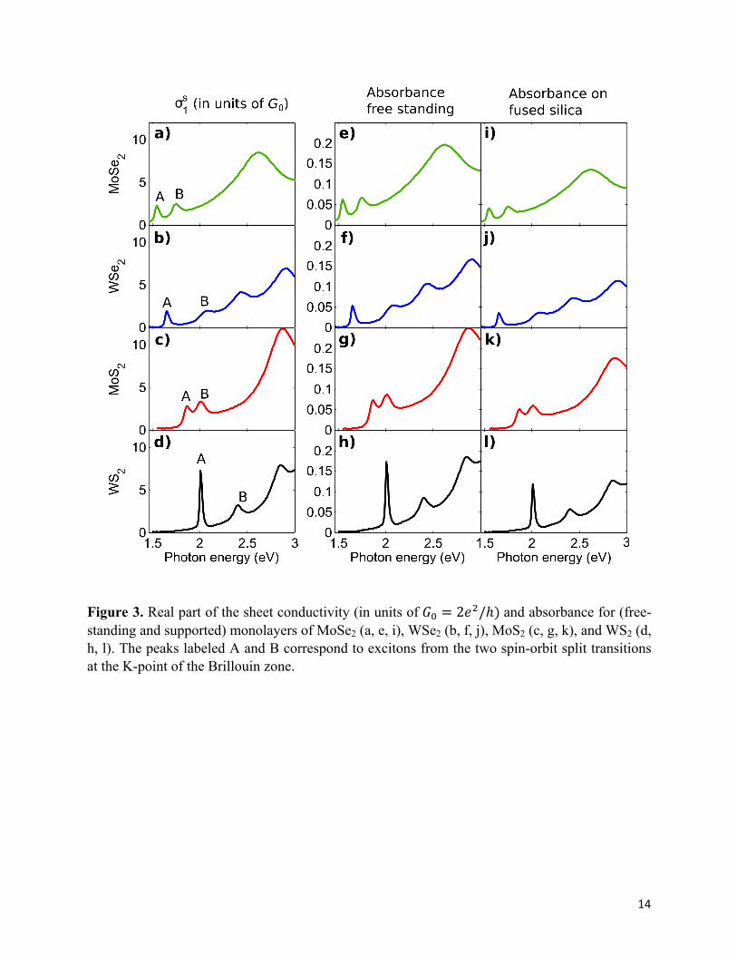
We can also express the material response in terms of the optical conductivity 𝜎 𝐸 =
𝜎% 𝐸 + 𝑖𝜎( 𝐸 = −𝑖(𝜀:𝐸/ℏ)[𝜀 𝐸 − 1]. We present this result in the form of the complex
sheet conductivity 𝜎@ 𝐸 ≡ 𝜎 𝐸 𝑑, where d denotes the layer thickness. For a layer in which
there is no significant propagation effect for light passing through the material, i.e., 𝜀 𝐸C- (𝐸/
ℏ𝑐)𝑑 ≪ 1, the sheet conductivity provides a full description of the optical response. In Figs. 3(a-
d), we plot the real part of the sheet conductivity, 𝜎%@(𝐸), for the four TMDCs.
In Figs. 3(e-h) we present the absorption spectra for free-standing monolayers of the four
TMDC materials based on their measured dielectric functions. The overall absorbance (the
fraction of the incident light absorbed by the material) in this frequency range is on the order of
10% for all four materials, demonstrating strong light-matter interaction even for a monolayer. In
addition to these results for suspended monolayers, we have derived the absorbance for layers of
each material on the fused silica substrate, based on the same dielectric function for the
monolayers [Figs. 3 (i-l)]. The supported layers preserve the spectral shape for the absorbance
for the suspended layers. In terms of the magnitude, however, the supported layers absorb about
1/3 less than the corresponding suspended layers. This can be understood from the local field
correction factor of 4/(ns+1)2 for the light intensity above the substrate, where ns ≈ 1.46 is the
refractive index of fused silica.
V. DISCUSSION
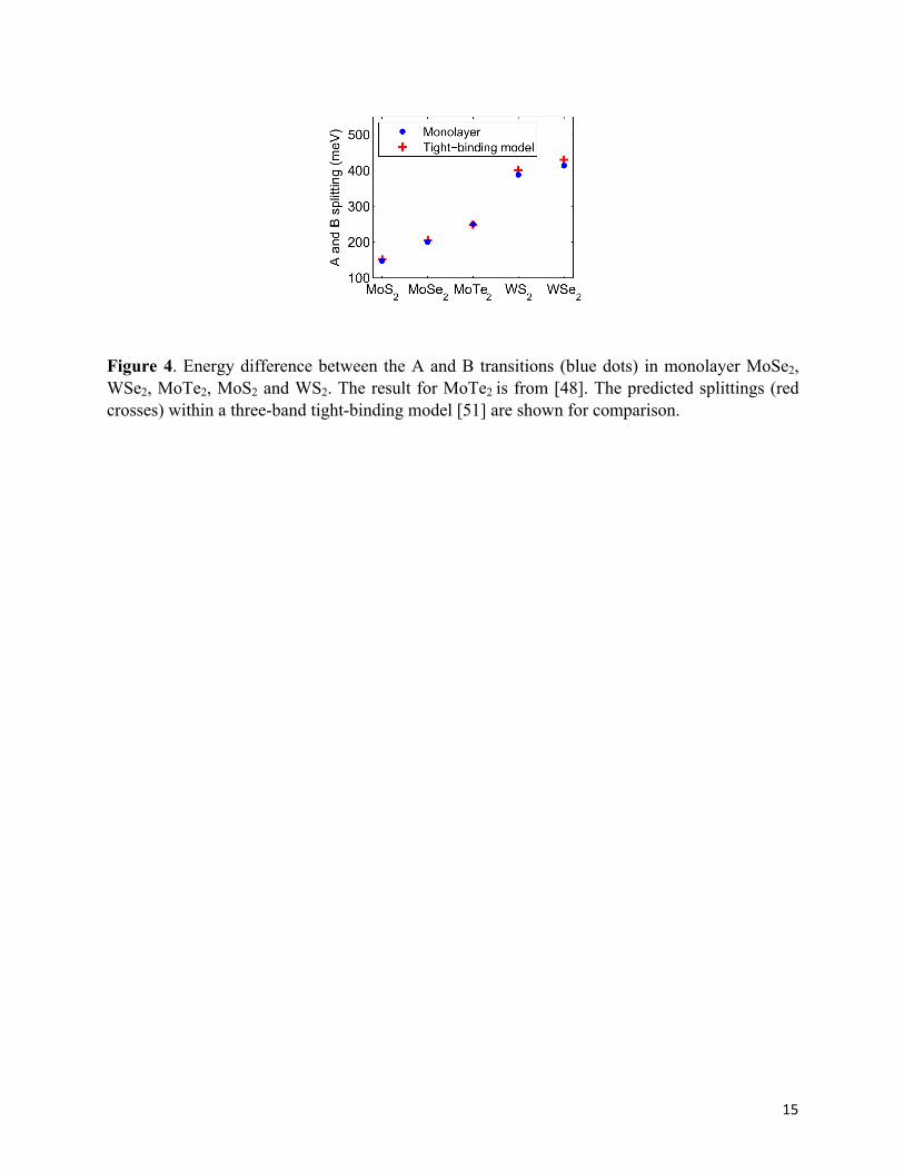
VA. EXTRACTION OF THE A-B SPLITTING
To extract quantitative properties of the excitonic resonances, we parameterize 𝜀( using a
small, but physically meaningful number of Lorentzians terms, allowing for an extraction of
transition energies of the excitonic features. [47] The resulting energy differences between the A
8
and B excitonic transitions are shown in Fig. 4 for the different monolayers. Results for the four
TMDC crystals, as well as for the exfoliated MoTe2 monolayers [48], are presented as a function
of the effective atomic number of the material, determined by weighting each element’s relative
contributions to the spin-orbit coupling [49].
The monolayer results correspond well with the previously reported data for MoS2, WS2,
and WSe2 monolayers [4,50]. The predicted A-B splitting from a three-band tight-binding model
[51] is also shown in Fig. 4. The good agreement between our experiment and the predictions of
the tight-binding model (fit to density functional calculations) is at first-sight surprising, since
these calculations neglect many-body Coulomb effects. However, the correction to the transition
energy from the (significant) exciton binding energy is largely offset by many-body corrections
to the quasi-particle band gap, rendering the predicted transition energy within a single-particle
calculation closer to experiment that might be expected. [52,53]
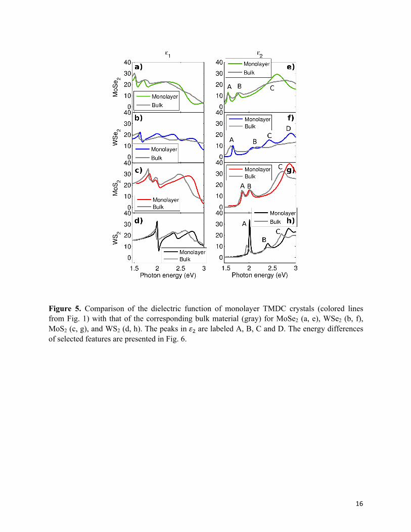
VB. COMPARISON WITH THE DIELECTRIC FUNCTION OF BULK MATERIAL
The dielectric functions for the monolayer TMDC crystals obtained in this work can be
compared with the dielectric functions for the corresponding bulk materials [45,46], as shown in
Fig. 5. While the dielectric functions for monolayer and bulk TMDCs show a significant overall
similarity, differences in the spectral responses are readily seen. There is a broadening of the
resonance features in the bulk materials comparing to the monolayers, which we attribute to the
additional optical transitions and carrier relaxation channels arising from interlayer coupling. On
the other hand, the total oscillator strength of the different features, which is proportional to the
integrated area of the imaginary part of the dielectric function, is largely conserved.
9
We also observed that the resonance energies in the monolayer dielectric function are
modestly shifted from the corresponding bulk material. In Fig. 6, we present the energy
difference between the spectral peaks in the imaginary part of the dielectric functions for
monolayers and the corresponding bulk material. We plot the A peak energy differences for
MoS2, MoSe2, WS2, and WSe2, the C peaks energy differences for MoS2, MoSe2, and WS2, and
D peak energy difference for WSe2. (The peak labels are shown in Fig. 5) We chose the D peak
instead of the C peak for WSe2 because the C peak in bulk WSe2 overlaps the B peak, hindering
an accurate determination of the peak energy. Comparing the monolayer to the bulk peak
energies, we see blue shifts for the C/D peak of 150 – 300 meV, while the shifts for the A peak
are in the range of 10 – 80 meV.
The qualitative trend of a shift of the peak energy to higher energies with decreasing
thickness can be understood as a quantum-confinement effect. As mentioned above, the net
many-body contribution to the transition energies is expected to be reduced significantly because
of the cancellation of electron-electron and electron-hole interactions. Consequently, in
considering the physical origin of the shift of the peaks from the bulk to the monolayer, we focus
on quantum-confinement effects in the band structure. The A peak corresponds to the excitons
located at the K-point in the Brillouin zone, which are composed primarily of the metal d-
orbitals. Thus the A exciton is spatially localized in the plane of the metal atoms [54] and
interlayer interactions in the bulk material do not lower the transition energy significantly. The
C/D feature is, however, associated with transitions away from the K-point and involves a
significant contribution from the chalcogen orbitals [38,49,54]. We therefore expect appreciably
stronger interlayer interactions in building up the bulk material from monolayers. This provides
a physical rationale for the larger observed red shift of the C/D transition compared to that of the
10
A exciton in comparing the bulk material to the monolayer. The behavior of the C/D transition
with increasing layer thickness is analogous to the quantum confinement effect of the lowest
indirect optical transition[4,5], which involves states at Γ-point of the Brillouin zone [55].
V. CONCLUSIONS
In conclusion, we have experimentally determined the complex in-plane dielectric
functions of monolayer MoS2, MoSe2, WS2 and WSe2, over photon energies between 1.5 eV and
3.0 eV. The dielectric functions imply strong light-matter interactions even in monolayers of
these TMDCs, with a peak absorbance of each of the four materials exceeding 15%. The A-B
exciton splitting is extracted from the measured dielectric function and is found to be in good
agreement with density functional calculations. Comparing to the bulk materials, we observed
only a slight red shift of the A feature, but a more significant shift of the higher-lying (C/D)
features. This behavior can be understood as a reflection of the different orbital character and
interlayer interactions of the wavefunctions relevant for the lower and higher energy transitions.
The authors acknowledge the U.S. Department of Energy, Office of Basic Energy
Sciences for support through Columbia Energy Frontier Research Center (grant DE-SC0001085)
for the preparation and characterization of samples; the National Science Foundation through
grants DMR-1122594 and DMR-1124894 for support for the optical measurements and data
analysis. H. M. H. and A. R. were supported, respectively, by the NSF through an IGERT
Fellowship (DGE-1069240) and by a Graduate Research Fellowship. A. C. acknowledges
funding from the Alexander von Humboldt Foundation through a Feodor-Lynen Fellowship. The

11
authors would like to thank Timothy C. Berkelbach, Tony Low, Dmytro Nykypanchuk, and
Xiaoxiao Zhang for fruitful discussions.
12
Figures:
Figure 1. Optical response of monolayers of MoSe2, WSe2, MoS2 and WS2 exfoliated on fused silica: (a-d) Measured reflectance spectra. (e-h) Real part of the dielectric function, 𝜀%. (i-l) Imaginary part of the dielectric function, 𝜀(. The peaks labeled A and B in (a-d) correspond to excitons from the two spin-orbit split transitions at the K-point of the Brillouin zone.
13
Figure 2. (a) Comparison of the reflectance spectra of two different exfoliated MoS2 monolayers. (b) Comparison of the reflectance spectra of exfoliated (red) and CVD-grown (blue) MoS2 monolayers.
14
Figure 3. Real part of the sheet conductivity (in units of 𝐺: = 2𝑒(/ℎ) and absorbance for (free-standing and supported) monolayers of MoSe2 (a, e, i), WSe2 (b, f, j), MoS2 (c, g, k), and WS2 (d, h, l). The peaks labeled A and B correspond to excitons from the two spin-orbit split transitions at the K-point of the Brillouin zone.
15
Figure 4. Energy difference between the A and B transitions (blue dots) in monolayer MoSe2, WSe2, MoTe2, MoS2 and WS2. The result for MoTe2 is from [48]. The predicted splittings (red crosses) within a three-band tight-binding model [51] are shown for comparison.
16
Figure 5. Comparison of the dielectric function of monolayer TMDC crystals (colored lines from Fig. 1) with that of the corresponding bulk material (gray) for MoSe2 (a, e), WSe2 (b, f), MoS2 (c, g), and WS2 (d, h). The peaks in 𝜀( are labeled A, B, C and D. The energy differences of selected features are presented in Fig. 6.

17
Figure 6. The observed blue shifts of features in the dielectric function of monolayer crystals of the TMDCs with respect to the corresponding bulk materials. The A peak denotes to the band-edge exciton at the K-point in the Brillouin zone and the C or D peak (depending on the material system, as discussed in the text) corresponds to the transitions away from the K-point.
18
References: [1] S. Z. Butler, S. M. Hollen, L. Cao, Y. Cui, J. A. Gupta, H. R. Gutiérrez, T. F. Heinz, S. S. Hong,
J. Huang, A. F. Ismach, E. Johnston-Halperin, M. Kuno, V. V. Plashnitsa, R. D. Robinson, R. S. Ruoff, S. Salahuddin, J. Shan, L. Shi, M. G. Spencer, M. Terrones, W. Windl, and J. E. Goldberger, ACS Nano 7, 2898 (2013).
[2] Q. H. Wang, K. Kalantar-Zadeh, A. Kis, J. N. Coleman, and M. S. Strano, Nat Nano 7, 699 (2012).
[3] X. Xu, W. Yao, D. Xiao, and T. F. Heinz, Nat Phys 10, 343 (2014). [4] K. F. Mak, C. Lee, J. Hone, J. Shan, and T. F. Heinz, Physical Review Letters 105, 136805
(2010). [5] A. Splendiani, L. Sun, Y. Zhang, T. Li, J. Kim, C.-Y. Chim, G. Galli, and F. Wang, Nano Letters
10, 1271 (2010). [6] K. F. Mak, K. He, J. Shan, and T. F. Heinz, Nat Nano 7, 494 (2012). [7] H. Zeng, J. Dai, W. Yao, D. Xiao, and X. Cui, Nat Nano 7, 490 (2012). [8] T. Cao, G. Wang, W. Han, H. Ye, C. Zhu, J. Shi, Q. Niu, P. Tan, E. Wang, B. Liu, and J. Feng,
Nat Commun 3, 887 (2012). [9] D. Xiao, G.-B. Liu, W. Feng, X. Xu, and W. Yao, Physical Review Letters 108, 196802 (2012). [10] A. Chernikov, T. C. Berkelbach, H. M. Hill, A. Rigosi, Y. Li, O. B. Aslan, D. R. Reichman, M. S.
Hybertsen, and T. F. Heinz, Physical Review Letters 113, 076802 (2014). [11] K. He, N. Kumar, L. Zhao, Z. Wang, K. F. Mak, H. Zhao, and J. Shan, Physical Review Letters
113, 026803 (2014). [12] K. F. Mak, K. He, C. Lee, G. H. Lee, J. Hone, T. F. Heinz, and J. Shan, Nat Mater 12, 207
(2013). [13] J. S. Ross, S. Wu, H. Yu, N. J. Ghimire, A. M. Jones, G. Aivazian, J. Yan, D. G. Mandrus, D.
Xiao, W. Yao, and X. Xu, Nat Commun 4, 1474 (2013). [14] M. M. Ugeda, A. J. Bradley, S.-F. Shi, F. H. da Jornada, Y. Zhang, D. Y. Qiu, W. Ruan, S.-K.
Mo, Z. Hussain, Z.-X. Shen, F. Wang, S. G. Louie, and M. F. Crommie, Nat Mater doi: 10.1038/nmat4061 advance online publication (2014).
[15] Z. Ye, T. Cao, K. O'Brien, H. Zhu, X. Yin, Y. Wang, S. G. Louie, and X. Zhang, Nature 513, 214 (2014).
[16] G. Wang, X. Marie, I. Gerber, T. Amand, D. Lagarde, L. Bouet, M. Vidal, A. Balocchi, and B. Urbaszek, arXiv:1404.0056 (2014).
[17] B. Zhu, X. Chen, and X. Cui, arXiv:1403.5108 (2014). [18] A. Pospischil, M. M. Furchi, and T. Mueller, Nat Nano 9, 257 (2014). [19] B. W. H. Baugher, H. O. H. Churchill, Y. Yang, and P. Jarillo-Herrero, Nat Nano 9, 262 (2014). [20] J. S. Ross, P. Klement, A. M. Jones, N. J. Ghimire, J. Yan, D. G. Mandrus, T. Taniguchi, K.
Watanabe, K. Kitamura, W. Yao, D. H. Cobden, and X. Xu, Nat Nano 9, 268 (2014). [21] L. Britnell, R. M. Ribeiro, A. Eckmann, R. Jalil, B. D. Belle, A. Mishchenko, Y. J. Kim, R. V.
Gorbachev, T. Georgiou, S. V. Morozov, A. N. Grigorenko, A. K. Geim, C. Casiraghi, A. H. C. Neto, and K. S. Novoselov, Science 340, 1311 (2013).
[22] C.-H. Lee, G.-H. Lee, A. M. van der Zande, W. Chen, Y. Li, M. Han, X. Cui, G. Arefe, C. Nuckolls, T. F. Heinz, J. Guo, J. Hone, and P. Kim, Nat Nano 9, 676 (2014).
[23] S. Jo, N. Ubrig, H. Berger, A. B. Kuzmenko, and A. F. Morpurgo, Nano Letters 14, 2019 (2014). [24] O. Lopez-Sanchez, E. Alarcon Llado, V. Koman, A. Fontcuberta i Morral, A. Radenovic, and A.
Kis, ACS Nano 8, 3042 (2014). [25] F. H. L. Koppens, T. Mueller, P. Avouris, A. C. Ferrari, M. S. Vitiello, and M. Polini, Nat Nano
9, 780 (2014). [26] S. Chih-Chiang, H. Yu-Te, L. Lain-Jong, and L. Hsiang-Lin, Applied Physics Express 6, 125801
(2013).

19
[27] C. Yim, apos, M. Brien, N. McEvoy, S. Winters, I. Mirza, J. G. Lunney, and G. S. Duesberg, Applied Physics Letters 104, 103114 (2014).
[28] W. Li, A. G. Birdwell, M. Amani, R. A. Burke, X. Ling, Y.-H. Lee, X. Liang, L. Peng, C. A. Richter, J. Kong, D. J. Gundlach, and N. V. Nguyen, arXiv:1407.6997 (2014).
[29] K. S. Novoselov, D. Jiang, F. Schedin, T. J. Booth, V. V. Khotkevich, S. V. Morozov, and A. K. Geim, Proceedings of the National Academy of Sciences of the United States of America 102, 10451 (2005).
[30] Y.-H. Lee, X.-Q. Zhang, W. Zhang, M.-T. Chang, C.-T. Lin, K.-D. Chang, Y.-C. Yu, J. T.-W. Wang, C.-S. Chang, L.-J. Li, and T.-W. Lin, Advanced Materials 24, 2320 (2012).
[31] Y. Zhan, Z. Liu, S. Najmaei, P. M. Ajayan, and J. Lou, Small 8, 966 (2012). [32] K.-K. Liu, W. Zhang, Y.-H. Lee, Y.-C. Lin, M.-T. Chang, C.-Y. Su, C.-S. Chang, H. Li, Y. Shi,
H. Zhang, C.-S. Lai, and L.-J. Li, Nano Letters 12, 1538 (2012). [33] X. Lu, J. Lin, M. I. B. Utama, X. Gong, J. Zhang, Y. Zhao, S. T. Pantelides, J. Wang, Z. Dong, Z.
Liu, W. Zhou, and Q. Xiong, Nano Letters 14, 2419 (2014). [34] C. Cong, J. Shang, X. Wu, B. Cao, N. Peimyoo, C. Qiu, L. Sun, and T. Yu, Advanced Optical
Materials 2, 131 (2014). [35] M. Bass, C. DeCusatis, J. Enoch, V. Lakshminarayanan, G. Li, C. MacDonald, V. Mahajan, and
E. Van Stryland, Handbook of Optics, Third Edition Volume IV: Optical Properties of Materials, Nonlinear Optics, Quantum Optics (set) (McGraw-Hill Education, 2009).
[36] J. A. Wilson and A. D. Yoffe, Advances in Physics 18, 193 (1969). [37] L. F. Mattheiss, Physical Review B 8, 3719 (1973). [38] D. Y. Qiu, F. H. da Jornada, and S. G. Louie, Physical Review Letters 111, 216805 (2013). [39] A. Carvalho, R. M. Ribeiro, and A. H. Castro Neto, Physical Review B 88, 115205 (2013). [40] E. Hecht, Optics (Addison-Wesley, San Francisco, CA, 2002), 4th edn., p.^pp. 426-428. [41] A. B. Kuzmenko, Review of Scientific Instruments 76 (2005). [42] G. Lucovsky, R. M. White, J. A. Benda, and J. F. Revelli, Physical Review B 7, 3859 (1973). [43] T. J. Wieting and J. L. Verble, Physical Review B 3, 4286 (1971). [44] B. Radisavljevic, A. Radenovic, J. Brivio, V. Giacometti, and A. Kis, Nat Nano 6, 147 (2011). [45] A. R. Beal and H. P. Hughes, Journal of Physics C: Solid State Physics 12, 881 (1979). [46] A. R. Beal, W. Y. Liang, and H. P. Hughes, Journal of Physics C: Solid State Physics 9, 2449
(1976). [47] See supplementary material at [] for the parameterization of the dielectric functions with
Lorentzian peaks and the A and B transition energies. [48] C. Ruppert, O. B. Aslan, and T. F. Heinz, Nano Letters (2014). [49] Z. Y. Zhu, Y. C. Cheng, and U. Schwingenschlögl, Physical Review B 84, 153402 (2011). [50] W. Zhao, Z. Ghorannevis, L. Chu, M. Toh, C. Kloc, P.-H. Tan, and G. Eda, ACS Nano 7, 791
(2012). [51] G.-B. Liu, W.-Y. Shan, Y. Yao, W. Yao, and D. Xiao, Physical Review B 88, 085433 (2013). [52] K. F. Mak, J. Shan, and T. F. Heinz, Physical Review Letters 106, 046401 (2011). [53] K. F. Mak, F. H. da Jornada, K. He, J. Deslippe, N. Petrone, J. Hone, J. Shan, S. G. Louie, and T.
F. Heinz, Physical Review Letters 112, 207401 (2014). [54] R. Coehoorn, C. Haas, and R. A. de Groot, Physical Review B 35, 6203 (1987). [55] W. Zhao, R. M. Ribeiro, M. Toh, A. Carvalho, C. Kloc, A. H. Castro Neto, and G. Eda, Nano
Letters 13, 5627 (2013).