mcn capabilities booklet
TRANSCRIPT
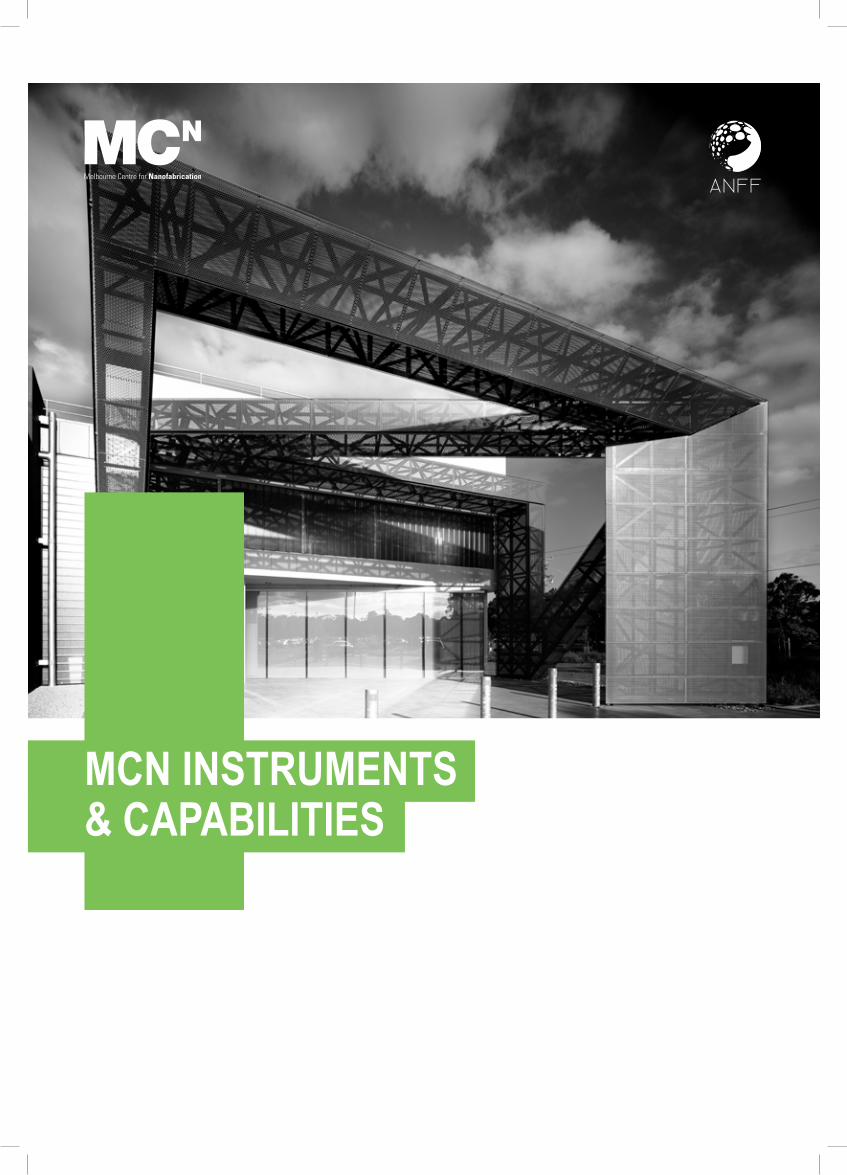
MCN INSTRUMENTS & CAPABILITIES

02/03
Etching 20/21Characterisation 22/23 Atomic force microscopy 24 Scanning electron microscopy 25 Spectroscopic ellipsometry 25 Laser doppler vibrometry 26 Profilometry 26 Laser scanning confocal microscopy 27 Hyperspectral imaging 27 Microspectrometry 28 Probe station 28 Scanning ion conductance microscopy 29 Laser TIRF 29 Particle sharacterisation 30 UV vis spectroscopy 30 Microarrayer 31 Zeta potential characterisation 31Packaging 32/33Access & Pricing 34
Biocapabilites 06/07 Biochemistry laboratory 06 PC2 laboratory 07 Swinburne Bioengineering Interface Hub 07Lithography 08/09 Focused ion beam lithography 10 Electron beam lithography 10 Hot embossing 11 Nano-imprint lithography 11 PDMS soft lithography 11 Direct write lithography 12 Automated wetbench suite 12 Photolithography 13 Spin coater and developer 13Thin film deposition 14/15 Atomic layer deposition 16 Sputtering 16 Electron beam evaporation 17 Polymer electronics glovebox 17 Furnace systems 18 Microwave enhanced diamond deposition 18 Thermal evaporation 19 Electroplating 19 Plasma enhanced chemical vapour deposition 19
CONTENTS
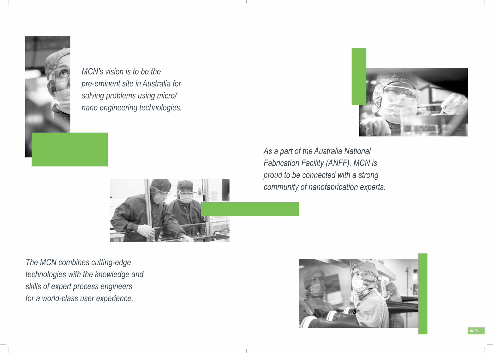
MCN’s vision is to be the pre-eminent site in Australia for solving problems using micro/nano engineering technologies.
As a part of the Australia National Fabrication Facility (ANFF), MCN is proud to be connected with a strong community of nanofabrication experts.
The MCN combines cutting-edge technologies with the knowledge and skills of expert process engineers for a world-class user experience.
04/05
BIOCAPABILITIES
BIOChEMISTRy LABORATORy
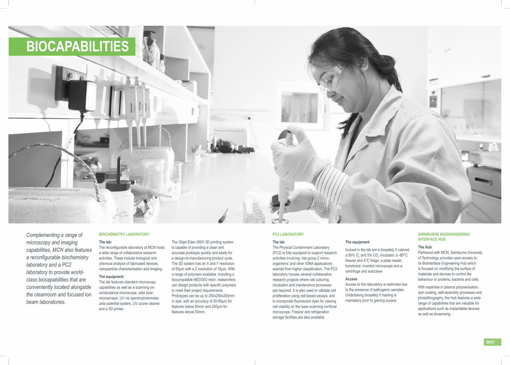
The lab: ThereconfigurablelaboratoryatMCNhostsa wide range of collaborative research activities. These include biological and chemical analysis of fabricated devices, nanoparticle characterisation and imaging.
The equipment: The lab features standard microscopy capabilities as well as a scanning ion conductance microscope, zeta sizer, microarrayer, UV vis spectrophotometer, zeta potential system, UV ozone cleaner and a 3D printer.
The Objet Eden 260V 3D printing system is capable of providing a clean and accurate prototype quickly and easily for a design-to-manufacturing product cycle. The 3D system has an X and Y resolution of 50µm with a Z resolution of 16µm. With a range of polymers available, including a biocompatible MEDGIO resin, researchers candesignproductswithspecificpolymersto meet their project requirements. Prototypes can be up to 250x250x200mm in size, with an accuracy of 20-85µm for features below 50mm and 200µm for features above 50mm.
Complementing a range of microscopy and imaging capabilities, MCN also features a reconfigurable biochemistry laboratory and a PC2 laboratory to provide world-class biocapabilities that are conveniently located alongside the cleanroom and focused ion beam laboratories.
PC2 LABORATORy
The lab The Physical Containment Laboratory (PC2) is fully equipped to support research activities involving ‘risk group 2 micro-organisms’ and other rDNA applications exemptfromhigherclassification.ThePC2laboratory houses several collaborative research projects where cell culturing, incubation and maintenance processes are required. It is also used to validate cell proliferation using cell-based assays, and toincorporatefluorescentdyesforviewingcell viability on the laser scanning confocal microscope. Freezer and refrigeration storage facilities are also available.
The equipment
Inclued in the lab are a biosafety II cabinet, a 95% O2 and 5% CO2 incubator, a -80OC freezer and 4OC fridge, a plate reader, fumehood, inverted microscope and a centrifuge and autoclave
AccessAccess to this laboratory is restricted due to the presence of pathogenic samples. Undertaking biosafety II training is mandatory prior to gaining access.
SwINBURNE BIOENgINEERINg INTERfACE hUB
The hubPartnered with MCN, Swinburne University of Technology provides open-access to its Biointerface Engineering Hub which is focused on modifying the surface of materials and devices to control the behaviour or proteins, bacteria and cells.
With expertise in plasma polymerisation, spin coating, self-assembly processes and photolithography, the Hub features a wide range of capabilities that are valuable for applications such as implantable devices as well as biosensing.
06/07

Micro-nano lithography is the process by which a pattern is written or transferred to a substrate. The process can be physical in nature, utilising a ‘stamp’ to press structures into a softer material, or chemical using light, ions or electron energy to write into photo and electron sensitive resists. This is necessary for the creation of the nanoscale components featured in nearly all modern technologies.
LIThOgRAPhy
PROCESS MAx RESOLUTION ENERgy USEd INSTRUMENT dEfININg fEATURE
Focused Ion Beam 5nm High energy Ga ions FEI Helios Nanolab600 Dual Beam FIB-SEM Ultra high resolution lithography using resist-free, direct write.
Electron Beam Lithography 7nm Electrons Vistec EBPG5000plusES Ultra high resolution lithography using direct write.
Hot Embossing 50nm Heat/Pressure EVG 520 IS Speedy pattern replication.
NanoImprint Lithography 15-30nm Heat/Pressure/UV EVG 520 IS or EVG6200 Speedy pattern replication on a smaller scale than hot embossing.
PDMS Soft Lithography 200 nm Heat PDMS Lab with Sylgard 184 Canbeusedforsurfaceswhicharenotflatduetoflexiblemold.
Direct Write Lithography 1µm UV Intelligent micropatterning SF100 XPRESS Versatility and speed for R&D.
Photo-lithography 1 - 5µm UV EVG6200 and SUSS MA-6 Aligning multi layer features using multiple masks.
Photo-lithography 5 µm UV ABM UV Flood Light Source Used for fast, lower resolution patterning.
08/09

fOCUSEd ION BEAM LIThOgRAPhy
The process High-resolution Focused Ion Beam (FIB)lithographyhassignificantadvantages as a single-step, nanoscale prototyping method that requires neither mask nor resist. It is capable of:
• Subtractive lithography in which atoms are locally milled away by physical sputtering with sub-10nm resolution
• Additive lithography in which materials are locally deposited with sub-10nm resolution
• Local ion implantation for fabrication of an etching mask
• Directmaterialmodificationby ion-induced mixing
The uses FIB lithography is a very versatile technique with a wide range of applications including
• Advanced materials development and characterisation
• Resist-free, high-resolution patterning of nanostructures
• Very precise, cross-sectional analysis • Sample preparation for transmission
electron microscopy (TEM) and for atom probe analysis
The instrument MCN’s FIB tool is the FEI Helios NanoLab 600 Dual Beam FIB-SEM. It features an ultra-high resolution Scanning Electron Microscope (SEM) and Focused Ion Beam (FIB) with various gas injection systems, including platinum deposition, selective carbon milling and metal-enhanced etching.
It also has a Genesis EDX detector to analyse the atomic composition of samples as well as a STEM detector, allowing the SEM to image very thin samples in transmission. This offers a great opportunity to acquire TEM comparable images with all the advantages of the SEM.
TheFIB-SEMhasbeenfittedwithadditional accessories - the Kleindiek Micromanipulator, which is an insertable probe that allows in-situ physical sample manipulation and characterisation at the nanoscale, and the Kleindiek Nanotechnik Lift-Out Shuttle, which provides in-situ lift-out sample preparation techniques for TEM and atom probe inspection. It features a high-resolution micro-gripper for easy transport and assembly of micro-sized objects.
ELECTRON BEAM LIThOgRAPhy
The process Electron Beam Lithography (EBL) allows users to write patterns with extremely high resolution, smaller than 10nm in size. It makes use of a highly energetic, tightly focused electron beam, which is scanned over a sample coated with an electron-sensitive resist. The electron beam scans theimageaccordingtoapatterndefinedonaCADfile.Thesampleisthendevelopedin an appropriate solvent which reveals the structuresdefinedintotheresist.Thisactsas a mold for subsequent pattern transfer techniques such as dry etching or metal lift-off.
The uses Due to the high-resolution nature of the technique, EBL has a vast range of applications including, but not limited to, nano-electronics, photonics, plasmonics, nano-fluidics,MEMS,x-rayandneutronoptics.
The instrument MCN’s EBL tool is the Vistec EBPG5000plusES, the only one of its kind in Australia. The tool is capable of writing four and six inch masks and wafers with a resolution of up to 10nm. It features 100kV acceleration voltage, automated aperture change and operation, 1mm mainfieldsizeand<20nmaccuracy.
NANO IMPRINT LIThOgRAPhy
The process Nanoimprint lithography involves refiningthehotembossingprocesstowork at a higher resolution. It can also be achieved by using a UV curable resist and subjecting the mold to UV light, rather than heat and pressure.
The uses This is useful in the creation of patterned media, optics, and lab on a chip systems.
The instruments Nanoimprint Lithography at MCN is performed on either the EVG 520IS or the EVG6200.
hOT EMBOSSINg
The process Hot embossing is a pattern-transfer technique, involving the application of pressure and heat to a resist-coated substrate, placed in contact with a master mold. This allows the relief features on the mold to be transferred faithfully into the resist. Once a pattern is made and the mold lifted off, the residual resist layer is dry etched away to leave a fully patterned resist. Hot embossing achieves fast patterning at a resolution of 50nm which is useful for projects which do not require ultra-high resolution.
The uses Hot embossing addresses a wide range of applications, from polymer-based lab-on-chip systems, where imprinting is done on thick polymers substrates, to the fabrication of sub 50nm features for bio-sensing or data recording applications,aswellasmicrofluidics,MEMS, optoelectronics, packaging and SOI production.
The instrument MCN’s hot embossing tool is the EVG520IS.
10/11
PdMS SOfT LIThOgRAPhy
The process: Soft lithography is a process by which rigid master mold structures, typically silicon/SU8, are replicated in an elastomeric material known as polydimethylsiloxane (PDMS). Silicon is exposed to the desired pattern using photoresist, after which the patterned structure is treated with an anti-stick coating and liquid PDMS is poured over it. Once cured, "daughter" devices can be removed from the mold whose features match that of the master.
The uses:Usefulforitsflexibility,PDMSisidealin applications involving surfaces which arenotflat.PDMScanalsobeusedinmicrofluidicapplications,whererapid prototyping is important. It is also biocompatible and oxygen permeable making it useful in a broad range of bio-applications, and it is optically transparent.
The lab: MCN has a dedicated PDMS Lab where Sylgard 184 is used.
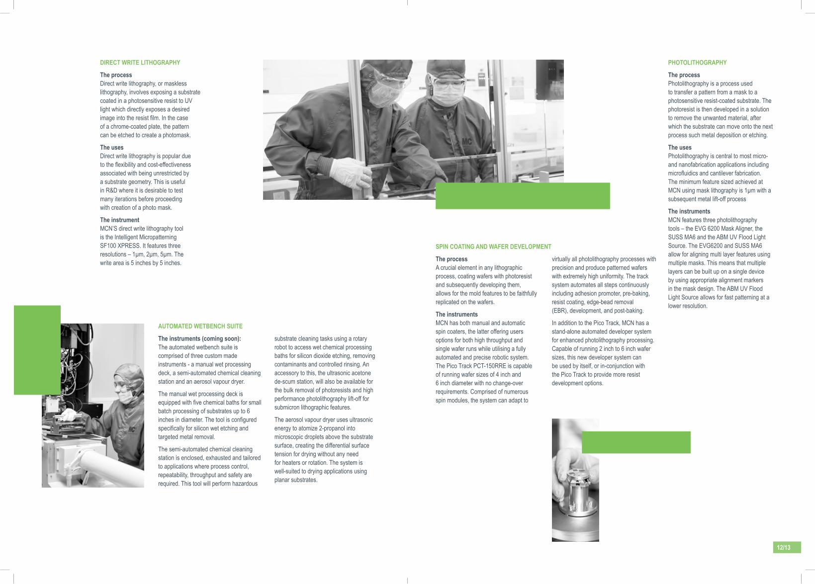
dIRECT wRITE LIThOgRAPhy
The process Direct write lithography, or maskless lithography, involves exposing a substrate coated in a photosensitive resist to UV light which directly exposes a desired imageintotheresistfilm.Inthecaseof a chrome-coated plate, the pattern can be etched to create a photomask.
The uses Direct write lithography is popular due totheflexibilityandcost-effectivenessassociated with being unrestricted by a substrate geometry. This is useful in R&D where it is desirable to test many iterations before proceeding with creation of a photo mask.
The instrument MCN’S direct write lithography tool is the Intelligent Micropatterning SF100 XPRESS. It features three resolutions – 1µm, 2µm, 5µm. The write area is 5 inches by 5 inches.
AUTOMATEd wETBENCh SUITE
The instruments (coming soon): The automated wetbench suite is comprised of three custom made instruments - a manual wet processing deck, a semi-automated chemical cleaning station and an aerosol vapour dryer.
The manual wet processing deck is equippedwithfivechemicalbathsforsmallbatch processing of substrates up to 6 inchesindiameter.Thetoolisconfiguredspecificallyforsiliconwetetchingandtargeted metal removal.
The semi-automated chemical cleaning station is enclosed, exhausted and tailored to applications where process control, repeatability, throughput and safety are required. This tool will perform hazardous
substrate cleaning tasks using a rotary robot to access wet chemical processing baths for silicon dioxide etching, removing contaminants and controlled rinsing. An accessory to this, the ultrasonic acetone de-scum station, will also be available for the bulk removal of photoresists and high performance photolithography lift-off for submicron lithographic features.
The aerosol vapour dryer uses ultrasonic energy to atomize 2-propanol into microscopic droplets above the substrate surface, creating the differential surface tension for drying without any need for heaters or rotation. The system is well-suited to drying applications using planar substrates.
SPIN COATINg ANd wAfER dEvELOPMENT
The process A crucial element in any lithographic process, coating wafers with photoresist and subsequently developing them, allows for the mold features to be faithfully replicated on the wafers.
The instruments MCN has both manual and automatic spin coaters, the latter offering users options for both high throughput and single wafer runs while utilising a fully automated and precise robotic system. The Pico Track PCT-150RRE is capable of running wafer sizes of 4 inch and 6 inch diameter with no change-over requirements. Comprised of numerous spin modules, the system can adapt to
virtually all photolithography processes with precision and produce patterned wafers with extremely high uniformity. The track system automates all steps continuously including adhesion promoter, pre-baking, resist coating, edge-bead removal (EBR), development, and post-baking.
In addition to the Pico Track, MCN has a stand-alone automated developer system for enhanced photolithography processing. Capable of running 2 inch to 6 inch wafer sizes, this new developer system can be used by itself, or in-conjunction with the Pico Track to provide more resist development options.
PhOTOLIThOgRAPhy
The process Photolithography is a process used to transfer a pattern from a mask to a photosensitive resist-coated substrate. The photoresist is then developed in a solution to remove the unwanted material, after which the substrate can move onto the next process such metal deposition or etching.
The uses Photolithography is central to most micro- and nanofabrication applications including microfluidicsandcantileverfabrication.The minimum feature sized achieved at MCN using mask lithography is 1µm with a subsequent metal lift-off process
The instruments MCN features three photolithography tools – the EVG 6200 Mask Aligner, the SUSS MA6 and the ABM UV Flood Light Source. The EVG6200 and SUSS MA6 allow for aligning multi layer features using multiple masks. This means that multiple layers can be built up on a single device by using appropriate alignment markers in the mask design. The ABM UV Flood Light Source allows for fast patterning at a lower resolution.
12/13
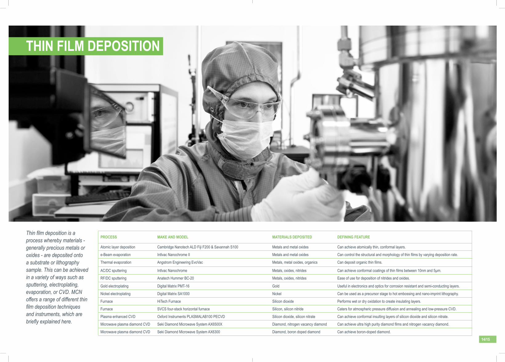
ThIN fILM dEPOSITION
Thin film deposition is a process whereby materials - generally precious metals or oxides - are deposited onto a substrate or lithography sample. This can be achieved in a variety of ways such as sputtering, electroplating, evaporation, or CVD. MCN offers a range of different thin film deposition techniques and instruments, which are briefly explained here.
PROCESS MAkE ANd MOdEL MATERIALS dEPOSITEd dEfININg fEATURE
Atomic layer deposition Cambridge Nanotech ALD Fiji F200 & Savannah S100 Metals and metal oxides Can achieve atomically thin, conformal layers.
e-Beam evaporation Intlvac Nanochrome II Metals and metal oxides Cancontrolthestructuralandmorphologyofthinfilmsbyvaryingdepositionrate.
Thermal evaporation Angstrom Engineering EvoVac Metals, metal oxides, organics Candepositorganicthinfilms.
AC/DC sputtering Intlvac Nanochrome Metals, oxides, nitrides Canachieveconformalcoatingsofthinfilmsbetween10nmand5µm.
RF/DC sputtering Anatech Hummer BC-20 Metals, oxides, nitrides Ease of use for deposition of nitrides and oxides.
Gold electroplating Digital Matrix PMT-16 Gold Useful in electronics and optics for corrosion resistant and semi-conducting layers.
Nickel electroplating Digital Matrix SA1000 Nickel Can be used as a precursor stage to hot embossing and nano-imprint lithography.
Furnace HiTech Furnace Silicon dioxide Performs wet or dry oxidation to create insulating layers.
Furnace SVCS four-stack horizontal furnace Silicon, silicon nitride Caters for atmospheric pressure diffusion and annealing and low-pressure CVD.
Plasma enhanced CVD Oxford Instruments PLASMALAB100 PECVD Silicon dioxide, silicon nitrate Can achieve conformal insulting layers of silicon dioxide and silicon nitrate.
Microwave plasma diamond CVD Seki Diamond Microwave System AX6500X Diamond, nitrogen vacancy diamond Canachieveultrahighpuritydiamondfilmsandnitrogenvacancydiamond.
Microwave plasma diamond CVD Seki Diamond Microwave System AX6300 Diamond, boron doped diamond Can achieve boron-doped diamond.
14/15
SPUTTERINg
The process Sputtering is a physical vapour deposition methodthatinvolvesdepositingthinfilmsin a vacuum environment. During this process, a solid material and substrate are positioned separately within a vacuum system. A high-energy argon ion plasma stream is targeted at the material, resulting in the subject material being ejected and deposited onto the substrate, creating a thinfilm.
As this is not an evaporative process, the temperatures required for sputtering are lower than evaporation methods. Thismakesitoneofthemostflexibledeposition processes and it is particularly useful for depositing materials with a high melting point or a mixture of materials, as compounds that may evaporate at different rates, can be sputtered at the samerate.Certainprocesseswillbenefitfromimprovedfilmadhesionduetohigherimpact energy.
The uses The sputtering process is used extensively in the semiconductor industry, screen displays, photovoltaics and magnetic data storage. Sputtering can be used to deposit awidevarietyofthinfilmsincludingmetals,oxides, nitrides and alloys.
The instruments MCN has two sputter deposition systems, the Intlvac Nanochrome AC/DC system and the Anatech Hummer BC-20 RF/DC System. These systems consist of a RF and dual AC and DC power supply and support samples sizes up to 8 inch diameter. Different process gases are available including argon, oxygen gas and nitrogen gas, allowing the deposition of pure metals, oxides, nitrides, alloys and customised combinatorial compositions.
In addition, the system also supports ion beam assisted deposition. The thickness of the coating can vary from ~10nm up to 5µm (thickness greater than 1µm should be discussed with the process engineer).
ATOMIC LAyER dEPOSITION
The process Atomic Layer Deposition (ALD) involves the deposition of materials one atomic monolayer at a time. It forms extremely uniform, conformal, pin-hole-free coatings on high aspect ratio structures. This is achieved by pulsing a chemical precursor onto a hydroxylated substrate surface. The precursor reacts with this surface but not with itself resulting in a monolayer of material. The precursor is purged from the chamber and then the surface is again hydroxylated with water vapour or oxygen, followed by another purge. These two steps are then repeated until the desired thickness of material is achieved.
The uses ALD has a vast array of applications from semiconductors, MEMS, nanostructures and optics through to wear-resistant coatings.
The instruments MCN has two ALD instruments – the Fiji F200 and the Savannah S100, both from Cambridge Nanotech. The Savannah system is thermal only and is integrated into a glovebox system so that samples can be kept in an inert environment. The Fiji F200 is capable of both thermal and Plasma Assisted ALD (PA-ALD).
PA-ALD expands the window for materials by decreasing activation energy and allows for deposition at lower temperatures to reduce precursor decomposition, depositiontimesandfilmcontaminations.Both systems are equipped to enable Cambridge Nanotech’s unique Exposure Mode™forthinfilmdepositiononultra high aspect ratio substrates.
ELECTRON BEAM EvAPORATION
The process Electron-beam evaporation is a physical vapour deposition method for depositingthinfilmsofmetals,oxidesand semiconductors in a high vacuum environment. Ultra high purity coating material is placed inside a vacuum chamber, typically as pellets in a crucible. Electron energy is used to heat these pellets, causing the coating material to enter the gas phase. Due to the vacuum environment, the evaporated particles can travel to the substrate without colliding with foreign particles, where they then condense onthesubstratesurfaceinathinfilm.
The uses Electron beam evaporation is used to depositelectronicandopticalfilmsforthe semiconductor industry and has
applications in displays and photovoltaics. High melting point materials can be deposited at high deposition rates, making this a preferred process for refractory metal andceramicfilms.
The instrument The Intlvac Nanochrome II electron beam evaporation system consists of a 10kV power supply and supports up to sixteen 4 inchwafersorfifteen6inchwafersorwafermounted samples. In addition, the system also supports ion beam assisted deposition andsubstratepre-cleaning.Singlefilmsor multi-material stacks are easily created usingsimplelayerdefinitions,whileuserscan also make use of ion-beam pre-cleaning and sample heating. Coating thickness are from 2nm up to 200nm (thickness >200nm by approval).
POLyMER ELECTRONICS gLOvEBOx
The instrument The Angstrom Engineering polymer dual glovebox system for polymer electronics fabrication provides an inert atmosphere for spin coating, electrode or counter-electrode deposition and assembly of organic photovoltaicandotherflexibleelectronicdevices. The glovebox system maintains a pure inert atmosphere by circulating drynitrogengasthroughapurifierandsolvent trap. Integrated into this system is a high vacuum chamber with mask transfer system for the thermal evaporative deposition of patterned electrodes and the ALD Savannah S100 system for counter electrode deposition.
The uses Useful for oxygen-sensitive chemistries and the assembly of organic photovoltaics and flexibletransistorfabrication.
16/17
fURNACE SySTEMS
The process Furnace systems are used to treat materials at high temperatures to change their properties through diffusion, annealing and chemical vapour deposition.
The instruments MCN has two furnace systems - the HiTech furnace and the SVCS four-stack horizontal furnace.
The HiTech furnace system is used to create layers of silicon dioxide on a silicon substrate. This can be achieved through wet or dry oxidation. In dry oxidation, the substrate is heated while oxygen is circulated over the surface, converting the surface layer of silicon to silicon dioxide. In wet oxidation, water is circulated over the surface and heated until the hydrogen evaporates, leaving behind oxygen to react with the silicon. Both methods achieve a
high-quality, even layer of silicon dioxide on a silicon substrate.
The HiTech furnace system can operate up to 1200oC and can perform dry oxidation (O2 is oxidant) and wet oxidation (steam is oxidant). The steam is generated with a torch that burns O2 and H2. The system can accept 3, 4 and 6 inch wafers.
The SVCS four-stack horizontal furnace system provides access to high temperature processing of silicon and other substrates, with small batch processing options. The four processing tubes cater for atmospheric pressure diffusion, atmospheric pressure annealing and the low-pressure chemical vapour deposition of low strain and stoichiometric silicon nitride. The tool has a HEPA controlled loading station.
MICROwAvE PLASMA ChEMICAL vAPOUR dIAMONd dEPOSITION
The process Diamond deposition is a chemical vapour deposition process which uses a continuous microwave source to heat hydrogen and carbon (in the form of methane) to between 700°C and 1000°C. This breaks down the atoms to become a highly reactive plasma. When the plasma interacts with an existing diamond sample surface, the hydrogen stabilises the diamond structure, while the methane adds new carbon to the diamond lattice. The systems are capable of fabricating either single or polycrystalline diamond as well as boron doped diamond.
The uses Diamond is highly useful in a wide range of applications, such the study of quantum phenomena, electronics and
medical bionics. Diamond is an ideal material for bionic devices as they need to be both biocompatible and suitable for long-term implant. It is a highly robust and hermetic material which makes it ideal for encasing and protecing electronics fromfluids.Furthemore,whendopedwithboron it can conduct energy, predisposing it to use in electronics and nitrogen vacancy diamond displays. These have interesting photoluminescence properties which can be exploited for quantum information systems.
The instruments MCN has two Seki Diamond Microwave Systems - AX6500X and AX6300. The AX6500X is used for growing ultra-high purity and nitrogen vacancy diamond, while the AX6300 is used for growing boron-
ELECTROPLATINg
The process Electroplating uses electrical current to reduce dissolved metal ions from an electrolyte to form a coherent metal coating on a material. The cathode, or part to be plated, and plating metal are immersed in an electrolyte containing dissolved metal salts as well as other ions that permit the flowofelectricity.Whenacurrentisappliedto the electrolyte, the free metal ions move through the solution to the cathode and are reduced to metal, creating a thin metal covering the surface.
The uses Electroplating is a common process in the jewellery, automotive, and food industries but it is also highly useful in the production of semi-conducting electronics and optics. Different metals can also be used to grow shims for use in hot embossing and nano-imprint lithography, while they can also help to protect surfaces from aggressive etching processes. Nickel electroplating can also be used to cast PDMS in the creation of fluidiccells.
The instruments MCN has the capability to provide high quality nickel and gold coatings and embossing shims using the Digital Matrix PMT-16 and SA1000.
ThERMAL EvAPORATION
The process Resistive thermal evaporation is another form of physical vapour deposition and can be used to deposit metals, organic, and inorganic polymers. In this method, electricalenergyisusedtoheatafilamentwhich in turn heats a deposition material to the point of evaporation. The process can be performed at very high levels of vacuum to eliminate collisions with foreign particles and therefore fewer tendencies to introduce filmimpurities.Highdepositionratescanbe achieved and lower energy particles can reduce substrate damage.
The uses Useful for the production of polymer solar cellsandflexibleelectronics.
The instrument
MCN’s thermal evaporation system is the Angstrom Engineering EvoVac. This system is integrated with glove box and has six resistive sources; three of which are standard resistive source locations and three of which are Luxel Radak furnaces. It supports sequential and co-deposition ofthinfilms.Thedepositionprocessiscontrolled using quartz rate sensors.
PLASMA ENhANCEd ChEMICAL vAPOUR dEPOSITION
The process Plasma Enhanced Chemical Vapour Deposition (PECVD) combines silicon with oxygen or nitrogen to create a plasma thatdepositsathinfilmofsilicondioxideor silicon nitrate onto a substrate. PECVD uses lower temperatures than the furnace systems to achieve an insulating layer on a variety of materials.
The uses PECVD is used in optics, microelectronics, energy applications, packaging and chemistry for the deposition of anti-reflectivecoatings,scratchresistanttransparent coatings, electronically
active layers, passivation layers, dielectric layers, isolating layers, etch stop layers, encapsulation and chemical protective coatings.
The instruments The PECVD system at MCN is an Oxford Instruments PLASMALAB100 PECVD and it is capable of depositing silicon dioxide and silicon nitride using a combination of gases. The system caters for a range of sample sizes up to and including 8 inch wafers. Deposition temperatures range from 25°C to 350°C.
18/19
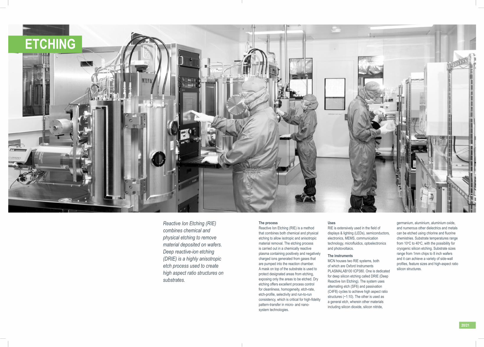
Reactive Ion Etching (RIE) combines chemical and physical etching to remove material deposited on wafers. Deep reactive-ion etching (DRIE) is a highly anisotropic etch process used to create high aspect ratio structures on substrates.
ETChINg
The process Reactive Ion Etching (RIE) is a method that combines both chemical and physical etching to allow isotropic and anisotropic material removal. The etching process is carried out in a chemically reactive plasma containing positively and negatively charged ions generated from gases that are pumped into the reaction chamber. A mask on top of the substrate is used to protect designated areas from etching, exposing only the areas to be etched. Dry etching offers excellent process control for cleanliness, homogeneity, etch-rate, etch-profile,selectivityandrun-to-runconsistency,whichiscriticalforhigh-fidelitypattern-transfer in micro- and nano-system technologies.
UsesRIEisextensivelyusedinthefieldofdisplays & lighting (LEDs), semiconductors, electronics, MEMS, communication technology,microfluidics,optoelectronicsand photovoltaics.
The instrumentsMCN houses two RIE systems, both of which are Oxford Instruments PLASMALAB100 ICP380. One is dedicated for deep silicon etching called DRIE (Deep Reactive Ion Etching). The system uses alternating etch (SF6) and passivation (C4F8) cycles to achieve high aspect ratio structures (~1:10). The other is used as a general etch, wherein other materials including silicon dioxide, silicon nitride,
germanium, aluminium, aluminium oxide, and numerous other dielectrics and metals canbeetchedusingchlorineandfluorinechemistries. Substrate temperatures range from 10oC to 40oC, with the possibility for cryogenic silicon etching. Substrate sizes range from 1mm chips to 8 inch wafers and it can achieve a variety of side-wall profiles,featuresizesandhigh-aspectratiosilicon structures.
20/21
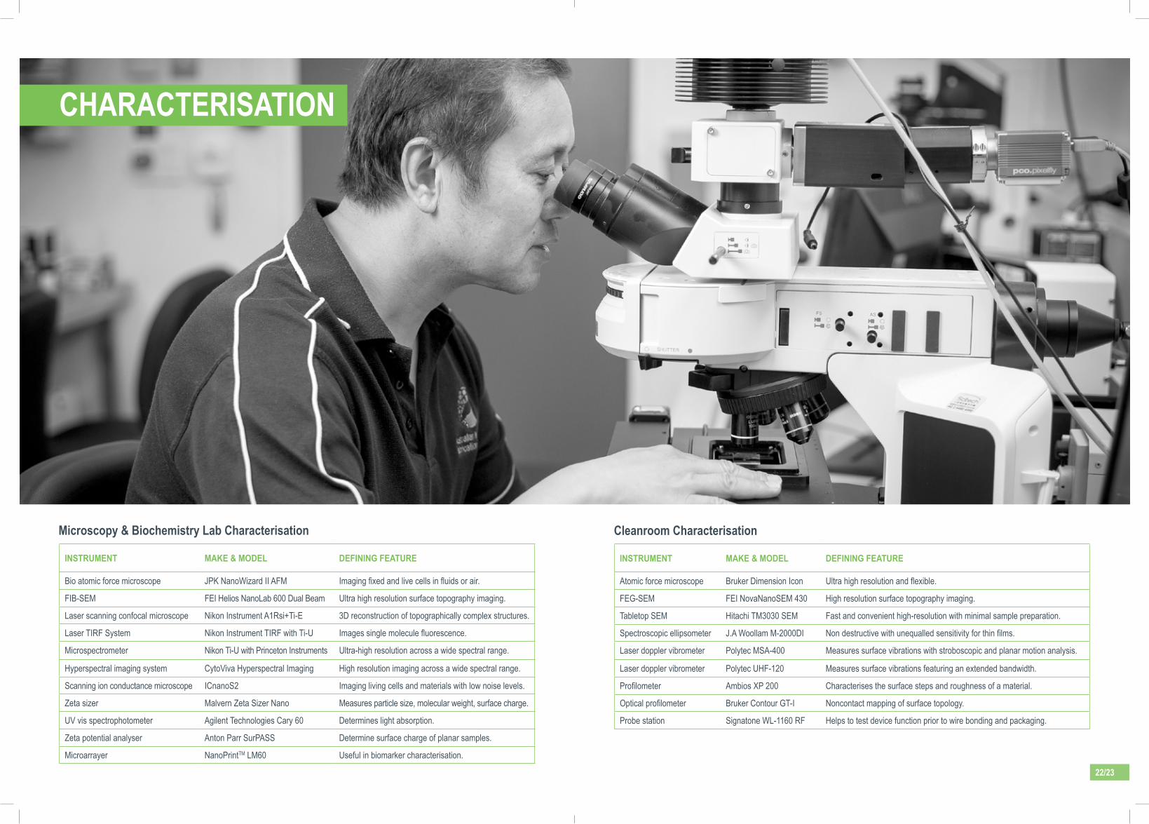
INSTRUMENT MAkE & MOdEL dEfININg fEATURE
Bio atomic force microscope JPK NanoWizard II AFM Imagingfixedandlivecellsinfluidsorair.
FIB-SEM FEI Helios NanoLab 600 Dual Beam Ultra high resolution surface topography imaging.
Laser scanning confocal microscope Nikon Instrument A1Rsi+Ti-E 3D reconstruction of topographically complex structures.
Laser TIRF System Nikon Instrument TIRF with Ti-U Imagessinglemoleculefluorescence.
Microspectrometer Nikon Ti-U with Princeton Instruments Ultra-high resolution across a wide spectral range.
Hyperspectral imaging system CytoViva Hyperspectral Imaging High resolution imaging across a wide spectral range.
Scanning ion conductance microscope ICnanoS2 Imaging living cells and materials with low noise levels.
Zeta sizer Malvern Zeta Sizer Nano Measures particle size, molecular weight, surface charge.
UV vis spectrophotometer Agilent Technologies Cary 60 Determines light absorption.
Zeta potential analyser Anton Parr SurPASS Determine surface charge of planar samples.
Microarrayer NanoPrintTM LM60 Useful in biomarker characterisation.
ChARACTERISATION
Microscopy & Biochemistry Lab Characterisation
INSTRUMENT MAkE & MOdEL dEfININg fEATURE
Atomic force microscope Bruker Dimension Icon Ultrahighresolutionandflexible.
FEG-SEM FEI NovaNanoSEM 430 High resolution surface topography imaging.
Tabletop SEM Hitachi TM3030 SEM Fast and convenient high-resolution with minimal sample preparation.
Spectroscopic ellipsometer J.A Woollam M-2000DI Nondestructivewithunequalledsensitivityforthinfilms.
Laser doppler vibrometer Polytec MSA-400 Measures surface vibrations with stroboscopic and planar motion analysis.
Laser doppler vibrometer Polytec UHF-120 Measures surface vibrations featuring an extended bandwidth.
Profilometer Ambios XP 200 Characterises the surface steps and roughness of a material.
Opticalprofilometer Bruker Contour GT-I Noncontact mapping of surface topology.
Probe station Signatone WL-1160 RF Helps to test device function prior to wire bonding and packaging.
22/23
Cleanroom Characterisation
ATOMIC fORCE MICROSCOPy
The process Atomic force microscopy (AFM) is an ultra-high resolution imaging technology and it is one of the most versatile characterisation methods. AFM performs scanning probe microscopy at a very high resolution scale, probing the surface of a material with a nanoscale cantilever either through direct contact or through oscillating the cantilever. When the cantilever is positioned in close proximity to the surface, forces between thetipandthesampleleadtodeflectionof the cantilever, which is then measured withalasersignalreflectedtoaphotodiodedetector. The properties of the material surface such as topography, mechanical properties and tip-surface interaction forces can then be generated leading to an understanding of the material surface at the nanoscale.
The uses AFM has a wide range of applications including nanoscale materials and surface characterisation, electrical materials characterisation, interaction forces and mechanical properties mapping. Bio AFM is useful for pharmaceutical studies, immunology studies, biosensing applications, antibody/antigen binding studies, as well as intra-molecular studies such as protein folding.
The instrumentsMCN has two AFM instruments – the Dimension Icon AFM which resides in the class 10,000 cleanroom and the NanoWizard II Bio AFM which resides in the Microscopy Lab.
The Dimension Icon AFM is designed with a large sample platform, providing the highest level of functionality, accessibility and performance, with ultra-low drift. It features a number of application modules such as ScanAsystTM, Peak Force QNMTM (PFQNM), electrical materials characterisation and heating and cooling studies. The ScanAsystTM imaging mode performs automatic image optimisation by controlling the tip-sample interaction force for easier, faster and more consistent imaging results. The PFQNM mode analyses tip-sample interaction forces and generates quantitative nanoscale maps of mechanical properties, including modulus, adhesion, deformation, and dissipation. PFQNM operates over an extremely wide range to characterise a large variety of sample types. The AFM executes temperature control and thermal analysis on samples from -35°C to 250°C while scanning in various AFM modes.
The Nanowizard II Bio AFM is designed forimagingfixedandlivecellsinairorbiologicalorchemicalfluids.Itcanbeused to understand surface chemistry of cells and measure force spectroscopy of surfaces. It is able to take measurements at variable temperatures with the possibility of perfusion. The system features stand-alonetipscanning,allowingforflexibilityin applications whilst maintaining high resolutions as well as a large scan fieldof100x100x15µm. It can also be integrated with the laser scanning confocal microscope.
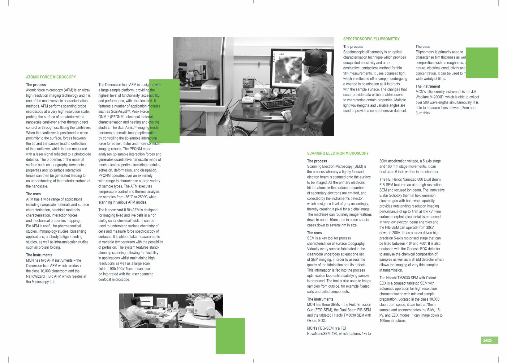
SCANNINg ELECTRON MICROSCOPy
The process Scanning Electron Microscopy (SEM) is the process whereby a tightly focused electron beam is scanned onto the surface to be imaged. As the primary electrons hit the atoms in the surface, a number of secondary electrons are emitted, and collected by the instrument’s detector, which assigns a level of grey accordingly, thereby creating a pixel for a digital image. The machines can routinely image features down to about 10nm, and in some special cases down to several nm in size.
The usesSEM is a key tool for process characterisation of surface topography. Virtually every sample fabricated in the cleanroom undergoes at least one set of SEM imaging, in order to assess the quality of the fabrication and its defects. This information is fed into the process optimisation loop until a satisfying sample is produced. The tool is also used to image samplesfromoutside,forexamplefixatedcells and failed components.
The instruments MCN has three SEMs – the Field Emission Gun (FEG-SEM), the Dual Beam FIB-SEM and the tabletop Hitachi TM3030 SEM with Oxford EDX.
MCN’s FEG-SEM is a FEI NovaNanoSEM-430, which features 1kv to
30kV acceleration voltage, a 5 axis stage and 100 mm stage movements. It can host up to 6 inch wafers in the chamber.
The FEI Helios NanoLab 600 Dual Beam FIB-SEM features an ultra-high resolution SEM and focused ion beam. The innovative ElstarSchottkythermalfieldemissionelectron gun with hot-swap capability provides outstanding resolution imaging performance of up to 1nm at low kV. Fine surface morphological detail is enhanced at very low electron beam energies and the FIB-SEM can operate from 30kV down to 200V. It has a piezo-driven high precision 5-axis motorised stage that can be tilted between -10o and +60o. It is also equipped with the Genesis EDX detector to analyse the chemical composition of samples as well as a STEM detector which allows the imaging of very thin samples in transmission.
The Hitachi TM3030 SEM with Oxford EDX is a compact tabletop SEM with automatic operation for high resolution characterisation with minimal sample preparation. Located in the class 10,000 cleanroom space, it can hold a 70mm sample and accommodates the 5-kV, 15-kV, and EDX modes. It can image down to 100nm structures.
SPECTROSCOPIC ELLIPSOMETRy
The process Spectroscopic ellipsometry is an optical characterisation technique which provides unequalled sensitivity and a non-destructive, contactless method for thin filmmeasurements.Itusespolarisedlightwhichisreflectedoffasample,undergoinga change in polarisation as it interacts with the sample surface. The changes that occur provide data which enables users to characterise certain properties. Multiple light wavelengths and variable angles are used to provide a comprehensive data set.
The usesEllipsometry is primarily used to characterisefilmthicknessaswellascomposition such as roughness, crystalline nature, electrical conductivity and doping concentration. It can be used to measure a widevarietyoffilms.
The instrument MCN’s ellipsometry instrument is the J.A Woollam M-2000DI which is able to collect over 500 wavelengths simultaneously. It is abletomeasurefilmsbetween2nmand3µm thick.
24/25
LASER dOPPLER vIBROMETRy
The process Laser Doppler Vibrometry (LDV) is used to measure the high frequency vibrations of surfaces by exploiting the Doppler shiftinreflectedlaserlight.ThisDopplershifted light provides information on the velocity, displacement, and phase of the surface vibrations.
The uses LDV is useful in the characterisation of MEMS devices, as well as piezoelectrics and surface acoustic wave devices.
The instrumentsMCN has two Polytec LDVs - the MSA-400 and UHF-120.
The MSA-400 features a fully integrated system, combining a microscope with
scanning laser doppler vibrometry and stroboscopic video microscopy for planar motion analysis. This all-in-one combination oftechnologiesclarifiestherealmicrostructural response of an oscillating system. Utilised in the MEMS device design cycle, the MSA-400 provides precise 3D dynamic and static response data that simplifiestroubleshooting,enhancesandshortens design cycles, improves yield and performance, and reduces product cost.
The UHF-120 has a much larger bandwidth allowing for characterisation of samples with a 1µm diameter at ultra-high frequencies of up to 1.2 GHz. This tool is equipped with a motorised stage and is not equipped with the stroboscopic or planar motion analysis option.
PROfILOMETRy
The process Profilometryisusedtocharacterisethesurface steps and the roughness of a material. Both contact and non-contact, or opticalprofilometry,areavailableatMCN.
ThestylusprofilometeravailableatMCNuses a direct contact method to register slight changes in the surface height of a material. This is achieved by dragging a metal tip along the surface of a sample and measuring the distance traced by the stylus tipanditsdeflectionalongtheverticalaxis.This measurement is then converted into a cross-sectional plot and can be used to resolve steps as small as 10nm.
Opticalprofilometryemploysphase-shiftingand/or vertical scanning interferometry to resolve the topology of complex 3D structures. The technique marries precision z-axis control with interference based techniques to resolve features from the angstrom to millimetre scale. The technique lends itself well to die-based measurements for ISO/QA and large area mapping.
The usesProfilometryisusefulinprocesscontrolsteps such as measuring etch depth and lithography patterns.
The instrumentsMCN’stwoprofilometersaretheAmbiosXP 200 and the Bruker Contour GT-I.
The Ambios XP 200 features a 150x178mm motorised stage and is capable of performing 60mm in a single scan length, though it also features the possibility to stitch scans up to 150mm.
The Bruker Contour GT-I Optical Profilometerisafullyautomated,desktop optical microscope which measures surface features over a range of angles. The combination of tip/tilt in the head with automated staging and objectives, as well as vibration resistant measurement techniques, make the Contour GT-I ideal for measure on demand industrial requirements.
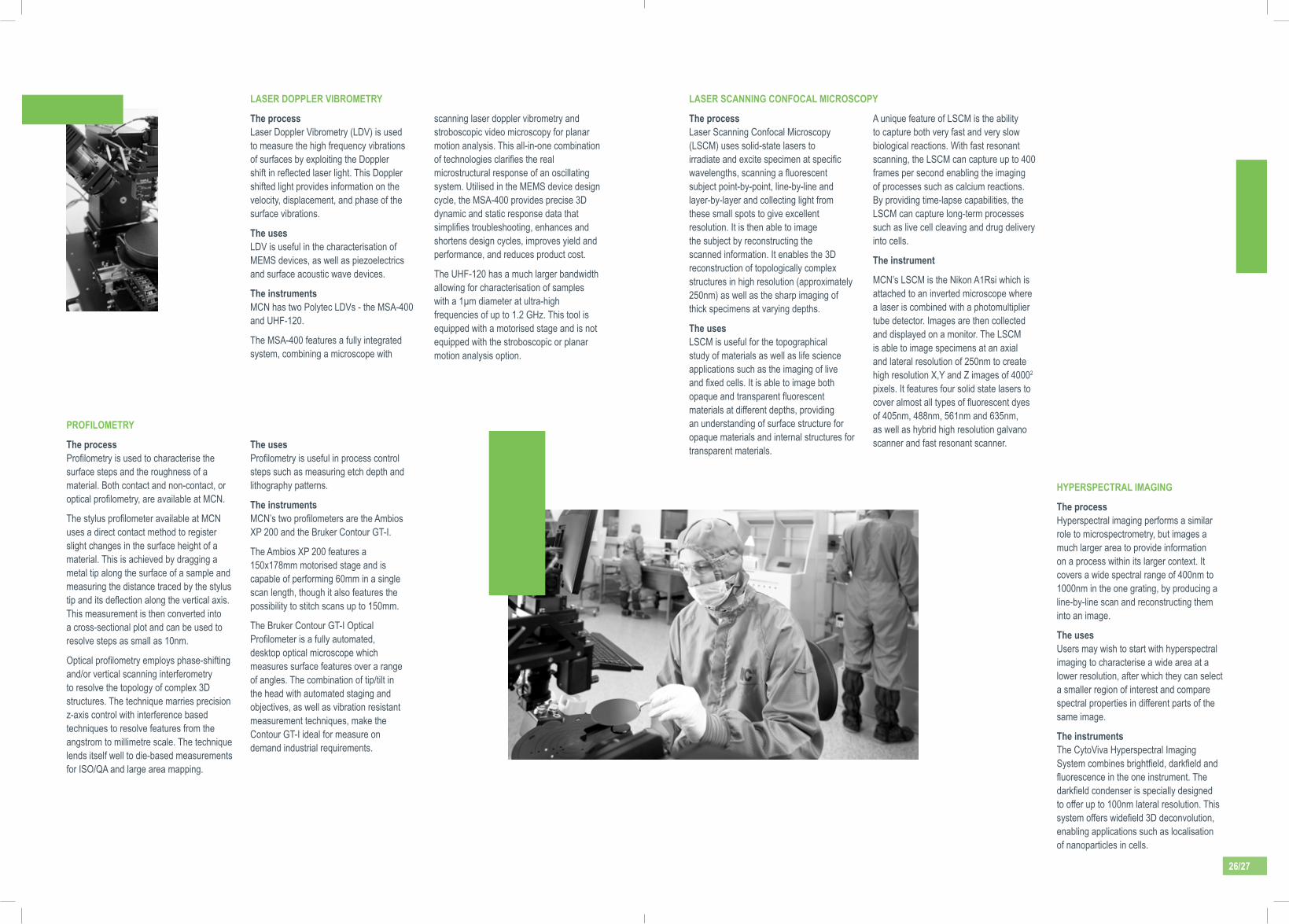
LASER SCANNINg CONfOCAL MICROSCOPy
The process Laser Scanning Confocal Microscopy (LSCM) uses solid-state lasers to irradiateandexcitespecimenatspecificwavelengths,scanningafluorescentsubject point-by-point, line-by-line and layer-by-layer and collecting light from these small spots to give excellent resolution. It is then able to image the subject by reconstructing the scanned information. It enables the 3D reconstruction of topologically complex structures in high resolution (approximately 250nm) as well as the sharp imaging of thick specimens at varying depths.
The usesLSCM is useful for the topographical study of materials as well as life science applications such as the imaging of live andfixedcells.Itisabletoimagebothopaqueandtransparentfluorescentmaterials at different depths, providing an understanding of surface structure for opaque materials and internal structures for transparent materials.
A unique feature of LSCM is the ability to capture both very fast and very slow biological reactions. With fast resonant scanning, the LSCM can capture up to 400 frames per second enabling the imaging of processes such as calcium reactions. By providing time-lapse capabilities, the LSCM can capture long-term processes such as live cell cleaving and drug delivery into cells.
The instrument
MCN’s LSCM is the Nikon A1Rsi which is attached to an inverted microscope where a laser is combined with a photomultiplier tube detector. Images are then collected and displayed on a monitor. The LSCM is able to image specimens at an axial and lateral resolution of 250nm to create high resolution X,Y and Z images of 40002 pixels. It features four solid state lasers to coveralmostalltypesoffluorescentdyesof 405nm, 488nm, 561nm and 635nm, as well as hybrid high resolution galvano scanner and fast resonant scanner.
hyPERSPECTRAL IMAgINg
The process Hyperspectral imaging performs a similar role to microspectrometry, but images a much larger area to provide information on a process within its larger context. It covers a wide spectral range of 400nm to 1000nm in the one grating, by producing a line-by-line scan and reconstructing them into an image.
The usesUsers may wish to start with hyperspectral imaging to characterise a wide area at a lower resolution, after which they can select a smaller region of interest and compare spectral properties in different parts of the same image.
The instrumentsThe CytoViva Hyperspectral Imaging Systemcombinesbrightfield,darkfieldandfluorescenceintheoneinstrument.Thedarkfieldcondenserisspeciallydesignedto offer up to 100nm lateral resolution. This systemofferswidefield3Ddeconvolution,enabling applications such as localisation of nanoparticles in cells.
26/27
PROBE STATION
The processProbe stations physically acquire signals from the electronic ports of semiconductor/RF/microwave devices. They utilise micro-manipulators which allow the precise positioning of thin needles on the surface ofadeviceorthinfilm.Whenadeviceisbeing electrically stimulated, the signal is acquired by the mechanical probe and is displayed on a supporting instrument such as an oscilloscope or network analyser.
The usesProbe stations are used primarily for researchanddevelopmentinthefieldsofelectronics and materials science. One of the main advantages of a probe station is the ability to test device function prior to wire bonding and packaging. It is therefore often used in the failure analysis and quality assurance testing of semiconductor/RF/microwave devices.
The instrumentsMCN’s probe station is a Signatone WL-1160 RF/Microwave. This probe station is designed for high-frequency (up to 67 Ghz), high-power, and millimetre wave applications where non-resonant operation is critical. It is also available for DC probing.Itisfittedwitha150mmdiametercircular chuck for holding a wide variety of sample sizes.
It includes a high-powered microscope for optimal viewing of the test area. Its key features include 150mm and 200mm manual X-Y motion control, 50x50mm microscope stage control and separate contact/plate height control with up to 30mm Z motion control of the plate. It holds up to four S-96MW microwave micropositioners and features a vibration damping table which eliminates vibration interference from outside.
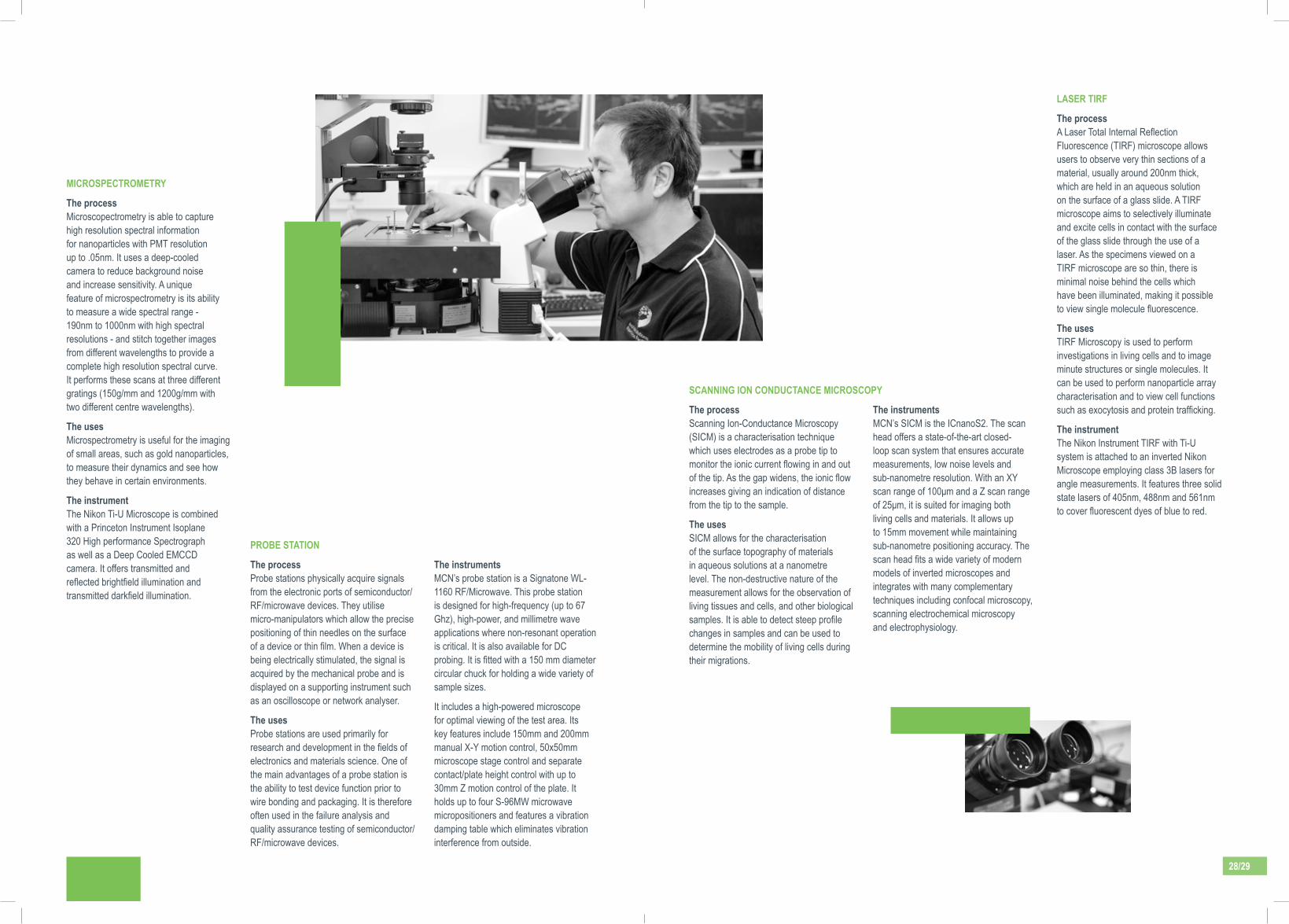
MICROSPECTROMETRy
The process Microscopectrometry is able to capture high resolution spectral information for nanoparticles with PMT resolution up to .05nm. It uses a deep-cooled camera to reduce background noise and increase sensitivity. A unique feature of microspectrometry is its ability to measure a wide spectral range - 190nm to 1000nm with high spectral resolutions - and stitch together images from different wavelengths to provide a complete high resolution spectral curve. It performs these scans at three different gratings (150g/mm and 1200g/mm with two different centre wavelengths).
The uses Microspectrometry is useful for the imaging of small areas, such as gold nanoparticles, to measure their dynamics and see how they behave in certain environments.
The instrumentThe Nikon Ti-U Microscope is combined with a Princeton Instrument Isoplane 320 High performance Spectrograph as well as a Deep Cooled EMCCD camera. It offers transmitted and reflectedbrightfieldilluminationandtransmitteddarkfieldillumination.
LASER TIRf
The process ALaserTotalInternalReflectionFluorescence (TIRF) microscope allows users to observe very thin sections of a material, usually around 200nm thick, which are held in an aqueous solution on the surface of a glass slide. A TIRF microscope aims to selectively illuminate and excite cells in contact with the surface of the glass slide through the use of a laser. As the specimens viewed on a TIRF microscope are so thin, there is minimal noise behind the cells which have been illuminated, making it possible toviewsinglemoleculefluorescence.
The usesTIRF Microscopy is used to perform investigations in living cells and to image minute structures or single molecules. It can be used to perform nanoparticle array characterisation and to view cell functions suchasexocytosisandproteintrafficking.
The instrument The Nikon Instrument TIRF with Ti-U system is attached to an inverted Nikon Microscope employing class 3B lasers for angle measurements. It features three solid state lasers of 405nm, 488nm and 561nm tocoverfluorescentdyesofbluetored.
SCANNINg ION CONdUCTANCE MICROSCOPy
The processScanning Ion-Conductance Microscopy (SICM) is a characterisation technique which uses electrodes as a probe tip to monitortheioniccurrentflowinginandoutofthetip.Asthegapwidens,theionicflowincreases giving an indication of distance from the tip to the sample.
The usesSICM allows for the characterisation of the surface topography of materials in aqueous solutions at a nanometre level. The non-destructive nature of the measurement allows for the observation of living tissues and cells, and other biological samples.Itisabletodetectsteepprofilechanges in samples and can be used to determine the mobility of living cells during their migrations.
The instrumentsMCN’s SICM is the ICnanoS2. The scan head offers a state-of-the-art closed-loop scan system that ensures accurate measurements, low noise levels and sub-nanometre resolution. With an XY scanrangeof100μmandaZscanrangeof25μm,itissuitedforimagingbothliving cells and materials. It allows up to 15mm movement while maintaining sub-nanometre positioning accuracy. The scanheadfitsawidevarietyofmodernmodels of inverted microscopes and integrates with many complementary techniques including confocal microscopy, scanning electrochemical microscopy and electrophysiology.
28/29
PARTICLE ChARACTERISATION
The process Particle characterisation is an important step in the study of nano-particulate systems. Measuring surface charge, or zeta potential, is necessary in the binding of materials as the zeta potential will determine what will adhere to it.
There are three processes which aid in the study of particle size, molecular weight and zeta potential. Dynamic light scattering is used to measure particle and molecule size by measuring the diffusion of particles moving under Brownian motion and converting this to size. Static light scattering is used to measure the molecular weight of proteins and polymers by measuring the scattering intensity of the molecules. Laser doppler micro-electrophoresis is used to measure surface charge, or zeta potential. This involves applying an electric fieldtoasolutionofparticlestoexcitethemand cause them to move. Their velocity is measured and their surface charge calculated accordingly.
The usesThe zeta sizer may be used in the study of organic and inorganic nanoparticles, ceramics, pigments and inks, emulsions and pharmaceuticals.
The instrumentsMCN’s particle characterisation instrument is the Malvern Zetasizer Nano ZS. It is a combined particle sizer and zeta potential unit that can measure the hydrodynamic size of particles (0.6nm – 6µm), the zeta potential of particles in the size range of 5nm – 10µm , as well as estimate the molecular weight of polymers and proteins up to 2 x 10⁷ Da with minimal sample volume. It is able to perform analysis and measurements of specimens in liquid suspensions while the system also features a fully automated titrator, allowing the measurement of zeta potential as a function of pH, conductivity or concentration of an additive.
Uv vIS SPECTROSCOPy
The process The ultraviolet visible spectrophotometer is used to determine a material’s energy absorption by measuring the percentage of light passing through a sample.
The usesIt can be used for quantitative analysis to work out the concentration of particles within a substance.
The instrumentsThe Agilent Cary UV vis spectrophotometer is capable of measuring absorbence for the wavelength range of 190nm to 1100nm. It provides exceptionally fast data collection, with a scan rate of up to 24,000 nm/min
ZETA POTENTIAL ChARACTERISATION
The process Solid surface analysis is important for determining electrokinetic potential of macroscopic solids where streaming potential and currents are measured. The instrument is capable of acquiring singlemeasurementsataspecificpHora titration, which can range for pH 2 to 12. With the availability of three mounts, a variety of samples ranging from solid surfaces to fabrics and powdered samples can be assessed.
The usesThe electrokinetic analyser can measure surface potential (zeta potential) of smooth surfaces and IsoElectric point of surfaces canalsobeidentified.Surfacepotentialof metal plates, ceramic tiles, wafers and thinfilmscanbemeasuredwithaclampingcell whereas for measurements of polymer membranes,filterstextilefabricsandminerals and rocks require an adjustable gap cell. A cylindrical cell can be acquired for measuring zeta potential of powdered and granular samples.
The instrumentsThe Anton Paar zeta potential analyser at MCN is available with a clamping cell, cylindrical and adjustable cell mount.
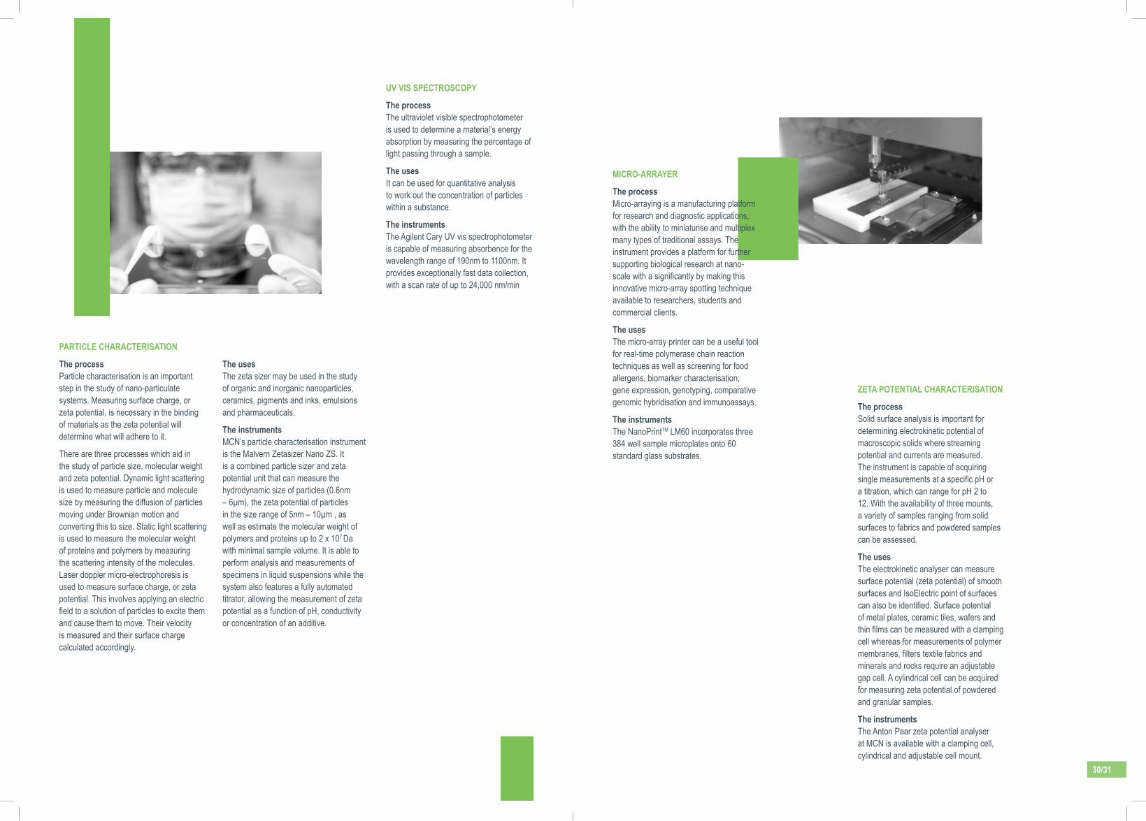
MICRO-ARRAyER
The processMicro-arraying is a manufacturing platform for research and diagnostic applications, with the ability to miniaturise and multiplex many types of traditional assays. The instrument provides a platform for further supporting biological research at nano-scalewithasignificantlybymakingthisinnovative micro-array spotting technique available to researchers, students and commercial clients.
The usesThe micro-array printer can be a useful tool for real-time polymerase chain reaction techniques as well as screening for food allergens, biomarker characterisation, gene expression, genotyping, comparative genomic hybridisation and immunoassays.
The instruments The NanoPrintTM LM60 incorporates three 384 well sample microplates onto 60 standard glass substrates.
30/31
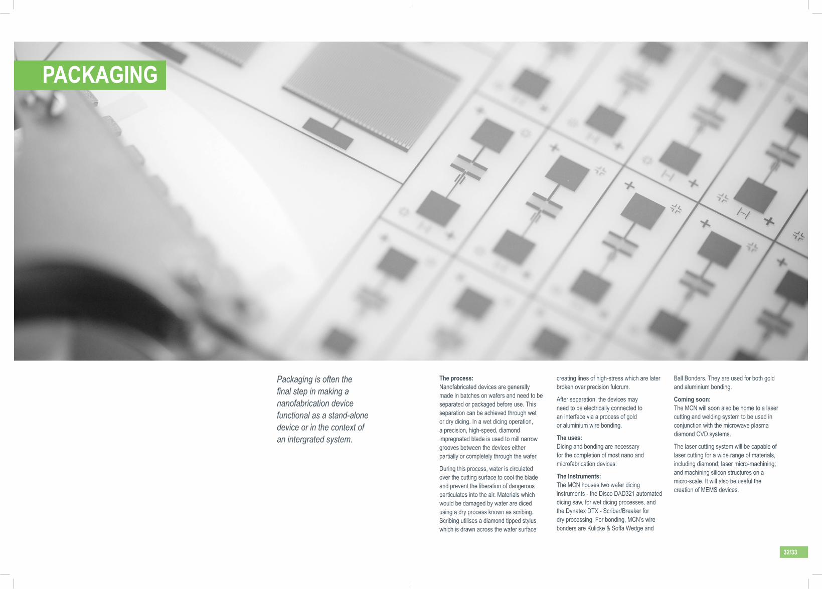
Packaging is often the final step in making a nanofabrication device functional as a stand-alone device or in the context of an intergrated system.
PACkAgINg
The process: Nanofabricated devices are generally made in batches on wafers and need to be separated or packaged before use. This separation can be achieved through wet or dry dicing. In a wet dicing operation, a precision, high-speed, diamond impregnated blade is used to mill narrow grooves between the devices either partially or completely through the wafer.
During this process, water is circulated over the cutting surface to cool the blade and prevent the liberation of dangerous particulates into the air. Materials which would be damaged by water are diced using a dry process known as scribing. Scribing utilises a diamond tipped stylus which is drawn across the wafer surface
creating lines of high-stress which are later broken over precision fulcrum.
After separation, the devices may need to be electrically connected to an interface via a process of gold or aluminium wire bonding.
The uses: Dicing and bonding are necessary for the completion of most nano and microfabrication devices.
The Instruments: The MCN houses two wafer dicing instruments - the Disco DAD321 automated dicing saw, for wet dicing processes, and the Dynatex DTX - Scriber/Breaker for dry processing. For bonding, MCN’s wire bonders are Kulicke & Soffa Wedge and
Ball Bonders. They are used for both gold and aluminium bonding.
Coming soon: The MCN will soon also be home to a laser cutting and welding system to be used in conjunction with the microwave plasma diamond CVD systems.
The laser cutting system will be capable of laser cutting for a wide range of materials, including diamond; laser micro-machining; and machining silicon structures on a micro-scale. It will also be useful the creation of MEMS devices.
32/33

If you think your R&D objectives would benefit from MCN’s experience and capabilities, we’d love to hear from you. Get in touch at [email protected] or visit www.nanomelbourne.com for more information on how to gain access to MCN. Please see the table below for access pricing and details:*
Tier 1 equipment includes: 3D printer, atomic force microscope, bio atomic force microscope, FEG-SEM, FIB-SEM, laser scanning confocal microscope, DRIE and RIE etchers, robotic wetbench dryer, mask aligners, nano imprint system, track robotic spin/bake/dev, ALD systems, electron beam evaporator, furnace stack, gold and nickel electroplating, PECVD, polymer glovebox, sputter systems and the thermal evaporator.
Tier 2 equipment includes: bio lab glovebox, hyperspectral imaging, laser doppler vibrometers, microspectrometer, opticalprofilometer,spectroscopicellipsometer, tabletop SEM, TIRF system, spin developer, dicing saw, scriber/breaker, wire bonders and the HiTech furnace.
Tier 3 equipment includes: microarray spotter, UV-vis spectrophotometer, zeta potential analyser, zeta sizer, mapping stagefilmetricssystem,metalwetetchbathtool, plasma asher, general laboratories, PC2laboratory,PDMSlaboratory,floodexposure unit and CNC milling.
* Pricing information accurate as at April 2015
dESCRIPTION ACAdEMIC/PUBLIC fUNdEd INdUSTRy
Tier 1 Equipment $90 / hour $225 / hour
Tier 2 Equipment $60 / hour $150 / hour
Tier 3 Equipment $40 / hour $100 / hour
MCN Staff Assistance $60 / hour $150 / hour
General Residency (by arrangement) $500 / month $1250 / month
Full Access Residency (by arrangement) $2000 / month $5000 / month
Flag ship Equipment:
•ElectronBeamLithography •UVLithography(excludingchromemask) •DiamondDeposition
$120 / hour ($1000 cap per run) $50 / hour ($350 cap per run) $90 / hour ($400 cap per 6 hrs)
$300 / hour ($2500 cap per run) $125 / hour ($850 cap per run) $225 / hour ($1000 cap per 6 hrs)
PRICINg
34/35
MCN is supported by:
MCN is partnered with:

W: www.nanomelbourne.comE: [email protected]: +613 9902 4073A: 151 Wellington rd, Clayton 3168