mc33887, 5.0 a h-bridge with load current · pdf file5.0 a h-bridge with load current feedback...
TRANSCRIPT

Document Number: MC33887Rev. 12.0, 2/2007
Freescale Semiconductor Technical Data
5.0 A H-Bridge with Load Current Feedback
The 33887 is a monolithic H-Bridge Power IC with a load current feedback feature making it ideal for closed-loop DC motor control. The IC incorporates internal control logic, charge pump, gate drive, and low RDS(ON) MOSFET output circuitry. The 33887 is able to control inductive loads with continuous DC load currents up to 5.0 A, and with peak current active limiting between 5.2 A and 7.8 A. Output loads can be pulse width modulated (PWM-ed) at frequencies up to 10 kHz. The load current feedback feature provides a proportional (1/375th of the load current) constant-current output suitable for monitoring by a microcontroller’s A/D input. This feature facilitates the design of closed-loop torque/speed control as well as open load detection.
A Fault Status output pin reports undervoltage, short circuit, and overtemperature conditions. Two independent inputs provide polarity control of two half-bridge totem-pole outputs. Two disable inputs force the H-Bridge outputs to tri-state (exhibit high impedance).
The 33887 is parametrically specified over a temperature range of -40°C ≤ TA ≤ 125°C and a voltage range of 5.0 V ≤ V+ ≤ 28 V. Operation with voltages up to 40 V with derating of the specifications.
Features• Fully specified operation 5.0 V to 28 V• Limited operation with reduced performance up to 40 V• 120 mΩ RDS(ON) Typical H-Bridge MOSFETs• TTL/CMOS Compatible Inputs• PWM Frequencies up to 10 kHz • Active Current Limiting (Regulation)• Fault Status Reporting• Sleep Mode with Current Draw ≤50 µA (Inputs Floating or Set
to Match Default Logic States)• Pb-Free Packaging Designated by Suffix Codes VW and EK
Figure 1. 33887 Simplified Application Diagram
ORDERING INFORMATION
Device Temperature Range (TA) Package
MC33887DH/R2
-40°C to 125°C
20 HSOPMC33887VW/R2
MC33887PNB/R2 36 PQFN
MC33887DWB/R254 SOICW-EP
MCZ33887EK/R2
DH SUFFIXVW SUFFIX (Pb-FREE)
98ASH70273A20-PIN HSOP
Bottom View
DWB SUFFIXEK SUFFIX (Pb-FREE)
98ASA10506D54-PIN SOICW-EP
PNB SUFFIX 98ASA10583D36-PIN PQFN
33887
H-BRIDGE
33887
CCP
IN1IN2D1
EN
FS
MCU
PGND
D2
MOTOR
OUT1
OUT2
AGND
V+
FB
6.0 VV+
FB
IN
OUT
OUT
OUT
OUT
OUT
A/D
Freescale Semiconductor, Inc. reserves the right to change the detail specifications, as may be required, to permit improvements in the design of its products. © Freescale Semiconductor, Inc., 2007. All rights reserved.

INTERNAL BLOCK DIAGRAM
INTERNAL BLOCK DIAGRAM
Figure 2. 33887 Simplified Internal Block Diagram
OUT1
OUT2
PGNDAGND
CCP VPWR
EN
IN1IN2D1
D2
FS
FB
CHARGE PUMP
CURRENTLIMIT,
OVERCURRENTSENSE &
FEEDBACKCIRCUIT
UNDERVOLTAGE
OVER
CONTROLLOGIC
TEMPERATURE
GATEDRIVE
5.0 VREGULATOR
25 µA
8 µA(EACH)
Analog Integrated Circuit Device Data 2 Freescale Semiconductor
33887
PIN CONNECTIONS
PIN CONNECTIONS
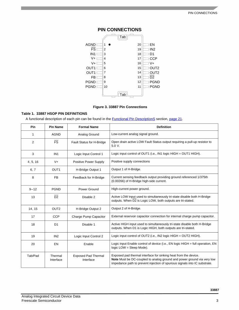
Figure 3. 33887 Pin Connections
Table 1. 33887 HSOP PIN DEFINITIONSA functional description of each pin can be found in the Functional Pin DescriptionS section, page 21.
Pin Pin Name Formal Name Definition
1 AGND Analog Ground Low-current analog signal ground.
2 FS Fault Status for H-Bridge Open drain active LOW Fault Status output requiring a pull-up resistor to 5.0 V.
3 IN1 Logic Input Control 1 Logic input control of OUT1 (i.e., IN1 logic HIGH = OUT1 HIGH).
4 , 5, 16 V+ Positive Power Supply Positive supply connections
6 , 7 OUT1 H-Bridge Output 1 Output 1 of H-Bridge.
8 FB Feedback for H-Bridge Current sensing feedback output providing ground referenced 1/375th (0.00266) of H-Bridge high-side current.
9 – 12 PGND Power Ground High-current power ground.
13 D2 Disable 2 Active LOW input used to simultaneously tri-state disable both H-Bridge outputs. When D2 is Logic LOW, both outputs are tri-stated.
14 , 15 OUT2 H-Bridge Output 2 Output 2 of H-Bridge.
17 CCP Charge Pump Capacitor External reservoir capacitor connection for internal charge pump capacitor.
18 D1 Disable 1 Active HIGH input used to simultaneously tri-state disable both H-Bridge outputs. When D1 is Logic HIGH, both outputs are tri-stated.
19 IN2 Logic Input Control 2 Logic input control of OUT2 (i.e., IN2 logic HIGH = OUT2 HIGH).
20 EN Enable Logic input Enable control of device (i.e., EN logic HIGH = full operation, EN logic LOW = Sleep Mode).
Tab/Pad Thermal Interface
Exposed Pad Thermal Interface
Exposed pad thermal interface for sinking heat from the device. Note Must be DC-coupled to analog ground and power ground via very low impedance path to prevent injection of spurious signals into IC substrate.
ENAGNDIN2D1CCPV+OUT2OUT2D2PGNDPGND
FS
V+OUT1OUT1
FBPGNDPGND
IN1V+
12345678910
2019
161514131211
1817
Tab
Tab
Analog Integrated Circuit Device Data Freescale Semiconductor 3
33887
PIN CONNECTIONS
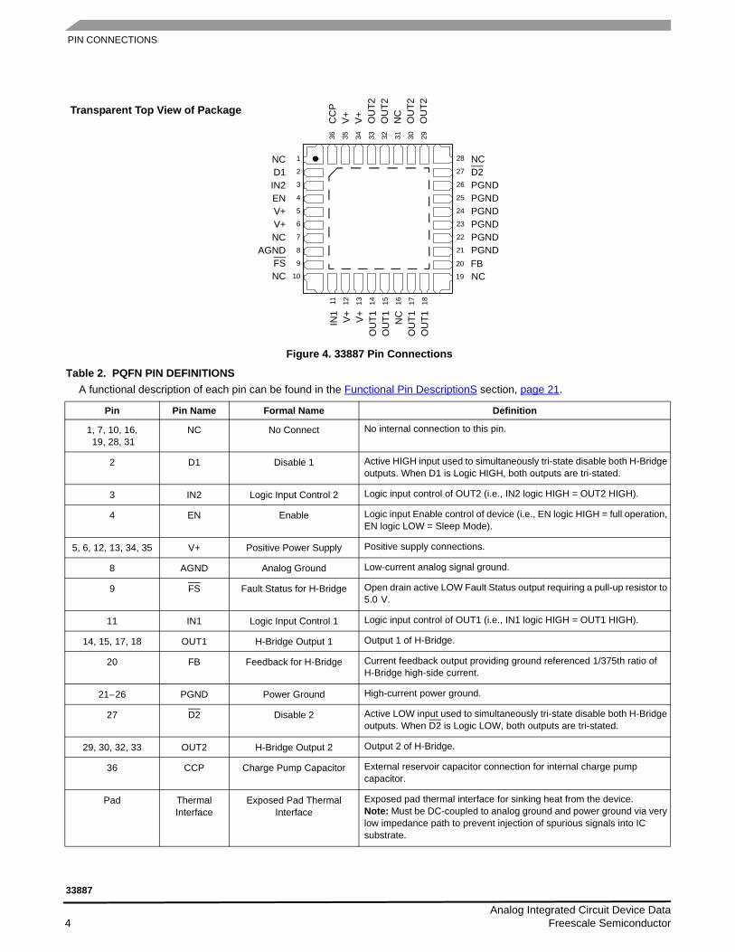
Figure 4. 33887 Pin Connections
Table 2. PQFN PIN DEFINITIONSA functional description of each pin can be found in the Functional Pin DescriptionS section, page 21.
Pin Pin Name Formal Name Definition
1, 7, 10, 16, 19, 28, 31
NC No Connect No internal connection to this pin.
2 D1 Disable 1 Active HIGH input used to simultaneously tri-state disable both H-Bridge outputs. When D1 is Logic HIGH, both outputs are tri-stated.
3 IN2 Logic Input Control 2 Logic input control of OUT2 (i.e., IN2 logic HIGH = OUT2 HIGH).
4 EN Enable Logic input Enable control of device (i.e., EN logic HIGH = full operation, EN logic LOW = Sleep Mode).
5, 6, 12, 13, 34, 35 V+ Positive Power Supply Positive supply connections.
8 AGND Analog Ground Low-current analog signal ground.
9 FS Fault Status for H-Bridge Open drain active LOW Fault Status output requiring a pull-up resistor to 5.0 V.
11 IN1 Logic Input Control 1 Logic input control of OUT1 (i.e., IN1 logic HIGH = OUT1 HIGH).
14, 15, 17, 18 OUT1 H-Bridge Output 1 Output 1 of H-Bridge.
20 FB Feedback for H-Bridge Current feedback output providing ground referenced 1/375th ratio of H-Bridge high-side current.
21– 26 PGND Power Ground High-current power ground.
27 D2 Disable 2 Active LOW input used to simultaneously tri-state disable both H-Bridge outputs. When D2 is Logic LOW, both outputs are tri-stated.
29, 30, 32, 33 OUT2 H-Bridge Output 2 Output 2 of H-Bridge.
36 CCP Charge Pump Capacitor External reservoir capacitor connection for internal charge pump capacitor.
Pad Thermal Interface
Exposed Pad Thermal Interface
Exposed pad thermal interface for sinking heat from the device. Note: Must be DC-coupled to analog ground and power ground via very low impedance path to prevent injection of spurious signals into IC substrate.
D2NC28
27
26
25
24
23
22
21
2
3
4
5
6
7
8
9
11 12 13 14 15 16 17 18
36 35 34 33 32 31 30 29
PGNDPGNDPGNDPGNDPGNDPGND
IN2 D1
ENV+V+NC
AGNDFS
V+
CC
P
V+
OU
T2O
UT2
NC
OU
T2O
UT2
V+
IN1
V+
OU
T1O
UT1 NC
OU
T1O
UT1
20 FB19 NC10NC
1NC
Transparent Top View of Package
Analog Integrated Circuit Device Data 4 Freescale Semiconductor
33887

PIN CONNECTIONS
Figure 5. 33887 Pin Connections
Table 3. SOICW-EP PIN DEFINITIONSA functional description of each pin can be found in the Functional Pin DescriptionS section, page 21.
Pin Pin Name Formal Name Definition
1– 4, 51– 54 PGND Power Ground High-current power ground.
5 – 7, 9, 14, 19 – 22, 27 – 29, 33 – 36, 41,
46, 48 – 50
NC No Connect No internal connection to this pin.
8 D2 Disable 2 Active LOW input used to simultaneously tri-state disable both H-Bridge outputs. When D2 is Logic LOW, both outputs are tri-stated.
10 – 13 OUT2 H-Bridge Output 2 Output 2 of H-Bridge.
15 – 18, 37 – 40 V+ Positive Power Supply Positive supply connections.
23 CCP Charge Pump Capacitor External reservoir capacitor connection for internal charge pump capacitor.
24 D1 Disable 1 Active HIGH input used to simultaneously tri-state disable both H-Bridge outputs. When D1 is Logic HIGH, both outputs are tri-stated.
25 IN2 Logic Input Control 2 Logic input control of OUT2 (i.e., IN2 logic HIGH = OUT2 HIGH).
26 EN Enable Logic input Enable control of device (i.e., EN logic HIGH = full operation, EN logic LOW = Sleep Mode).
30 AGND Analog Ground Low-current analog signal ground.
31 FS Fault Status for H-Bridge Open drain active LOW Fault Status output requiring a pull-up resistor to 5.0 V.
32 IN1 Logic Input Control 1 Logic input control of OUT1 (i.e., IN1 logic HIGH = OUT1 HIGH).
PGND
NCV+V+V+V+NCNCNCNC
CCPD1
IN2ENNC
NC
NCOUT2OUT2OUT2OUT2
NCNCD2
PGNDPGND
PGNDPGND
NCV+V+V+V+NCNCNCNCIN1FSAGNDNCNC
NC
NCOUT1OUT1OUT1OUT1
NCNCFB
PGNDPGND
PGND54
40
.3534333231302928
39383736
47464544434241
51504948
5352
1
15
2021222324252627
16171819
891011121314
4567
23
Transparent Top View of Package
Analog Integrated Circuit Device Data Freescale Semiconductor 5
33887

PIN CONNECTIONS
42 – 45 OUT1 H-Bridge Output 1 Output 1 of H-Bridge.
47 FB Feedback for H-Bridge Current feedback output providing ground referenced 1/375th ratio of H-Bridge high-side current.
Pad Thermal Interface
Exposed Pad Thermal Interface
Exposed pad thermal interface for sinking heat from the device. Note Must be DC-coupled to analog ground and power ground via very low impedance path to prevent injection of spurious signals into IC substrate.
Table 3. SOICW-EP PIN DEFINITIONSA functional description of each pin can be found in the Functional Pin DescriptionS section, page 21.
Pin Pin Name Formal Name Definition
Analog Integrated Circuit Device Data 6 Freescale Semiconductor
33887

ELECTRICAL CHARACTERISTICSMAXIMUM RATINGS
ELECTRICAL CHARACTERISTICS
MAXIMUM RATINGS
MAXIMUM RATINGS All voltages are with respect to ground unless otherwise noted.
Rating Symbol Value UnitELECTRICAL RATINGS
Supply Voltage (1) V+ -0.3 to 40 V
Input Voltage (2) VIN - 0.3 to 7.0 VFS Status Output (3) V FS -0.3 to 7.0 VContinuous Current (4) IOUT 5.0 ADH Suffix HSOP ESD Voltage (5)
Human Body Model Each Pin to AGNDEach Pin to PGNDEach Pin to V+Each I/O to All Other I/Os
Machine Model
VESD1VESD1VESD1VESD1VESD2
±1000±1500±2000±2000±200
V
VW Suffix HSOP, SOICW-EP, and PQFN ESD Voltage (5)
Human Body Model Machine Model
VESD1VESD2
± 2000± 200
V
THERMAL RATINGS
Storage Temperature TSTG - 65 to 150 °C Operating Temperature (6)
Ambient Junction
TATJ
- 40 to 125- 40 to 150
°C
Peak Package Reflow Temperature During Reflow (7), (8) TPPRT Note 8. °C
Notes1 Performance at voltages greater than 28V is degraded.See Electrical Performance Curves on page 18 and 19 for typical performance.
Extended operation at higher voltages has not been fully characterized and may reduce the operational lifetime.2 Exceeding the input voltage on IN1, IN2, EN, D1, or D2 may cause a malfunction or permanent damage to the device.3 Exceeding the pull-up resistor voltage on the open Drain FS pin may cause permanent damage to the device.4 Continuous current capability so long as junction temperature is ≤ 150°C.5 ESD1 testing is performed in accordance with the Human Body Model (CZAP = 100 pF, RZAP = 1500 Ω), ESD2 testing is performed in
accordance with the Machine Model (CZAP = 200 pF, RZAP = 0 Ω).6 The limiting factor is junction temperature, taking into account the power dissipation, thermal resistance, and heat sinking provided. Brief
nonrepetitive excursions of junction temperature above 150°C can be tolerated as long as duration does not exceed 30 seconds maximum. (nonrepetitive events are defined as not occurring more than once in 24 hours.)
7 Pin soldering temperature limit is for 10 seconds maximum duration. Not designed for immersion soldering. Exceeding these limits may cause malfunction or permanent damage to the device.
8. Freescale’s Package Reflow capability meets Pb-free requirements for JEDEC standard J-STD-020C. For Peak Package Reflow Temperature and Moisture Sensitivity Levels (MSL), Go to www.freescale.com, search by part number [e.g. remove prefixes/suffixes and enter the core ID to view all orderable parts. (i.e. MC33xxxD enter 33xxx), and review parametrics.
Analog Integrated Circuit Device Data Freescale Semiconductor 7
33887
ELECTRICAL CHARACTERISTICSMAXIMUM RATINGS
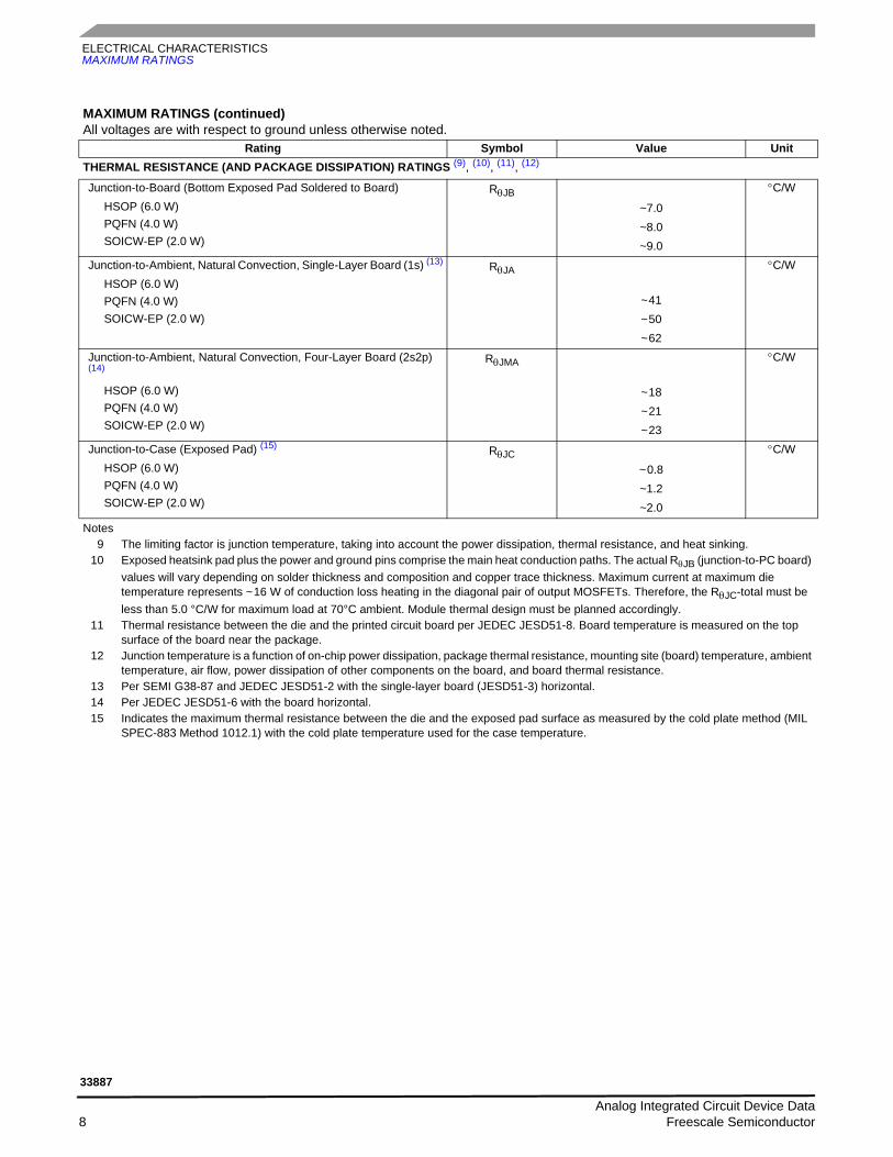
THERMAL RESISTANCE (AND PACKAGE DISSIPATION) RATINGS (9), (10), (11), (12)
Junction-to-Board (Bottom Exposed Pad Soldered to Board) HSOP (6.0 W)PQFN (4.0 W) SOICW-EP (2.0 W)
RθJB~7.0~8.0~9.0
°C/W
Junction-to-Ambient, Natural Convection, Single-Layer Board (1s) (13)
HSOP (6.0 W)PQFN (4.0 W) SOICW-EP (2.0 W)
RθJA
~ 41~ 50~ 62
°C/W
Junction-to-Ambient, Natural Convection, Four-Layer Board (2s2p) (14)
HSOP (6.0 W)PQFN (4.0 W) SOICW-EP (2.0 W)
RθJMA
~ 18~ 21~ 23
°C/W
Junction-to-Case (Exposed Pad) (15)
HSOP (6.0 W)PQFN (4.0 W) SOICW-EP (2.0 W)
RθJC~ 0.8~1.2~2.0
°C/W
Notes9 The limiting factor is junction temperature, taking into account the power dissipation, thermal resistance, and heat sinking.
10 Exposed heatsink pad plus the power and ground pins comprise the main heat conduction paths. The actual RθJB (junction-to-PC board) values will vary depending on solder thickness and composition and copper trace thickness. Maximum current at maximum die temperature represents ~ 16 W of conduction loss heating in the diagonal pair of output MOSFETs. Therefore, the RθJC-total must be less than 5.0 °C/W for maximum load at 70°C ambient. Module thermal design must be planned accordingly.
11 Thermal resistance between the die and the printed circuit board per JEDEC JESD51-8. Board temperature is measured on the top surface of the board near the package.
12 Junction temperature is a function of on-chip power dissipation, package thermal resistance, mounting site (board) temperature, ambient temperature, air flow, power dissipation of other components on the board, and board thermal resistance.
13 Per SEMI G38-87 and JEDEC JESD51-2 with the single-layer board (JESD51-3) horizontal.14 Per JEDEC JESD51-6 with the board horizontal.15 Indicates the maximum thermal resistance between the die and the exposed pad surface as measured by the cold plate method (MIL
SPEC-883 Method 1012.1) with the cold plate temperature used for the case temperature.
MAXIMUM RATINGS (continued)All voltages are with respect to ground unless otherwise noted.
Rating Symbol Value Unit
Analog Integrated Circuit Device Data 8 Freescale Semiconductor
33887
ELECTRICAL CHARACTERISTICSSTATIC ELECTRICAL CHARACTERISTICS
STATIC ELECTRICAL CHARACTERISTICS
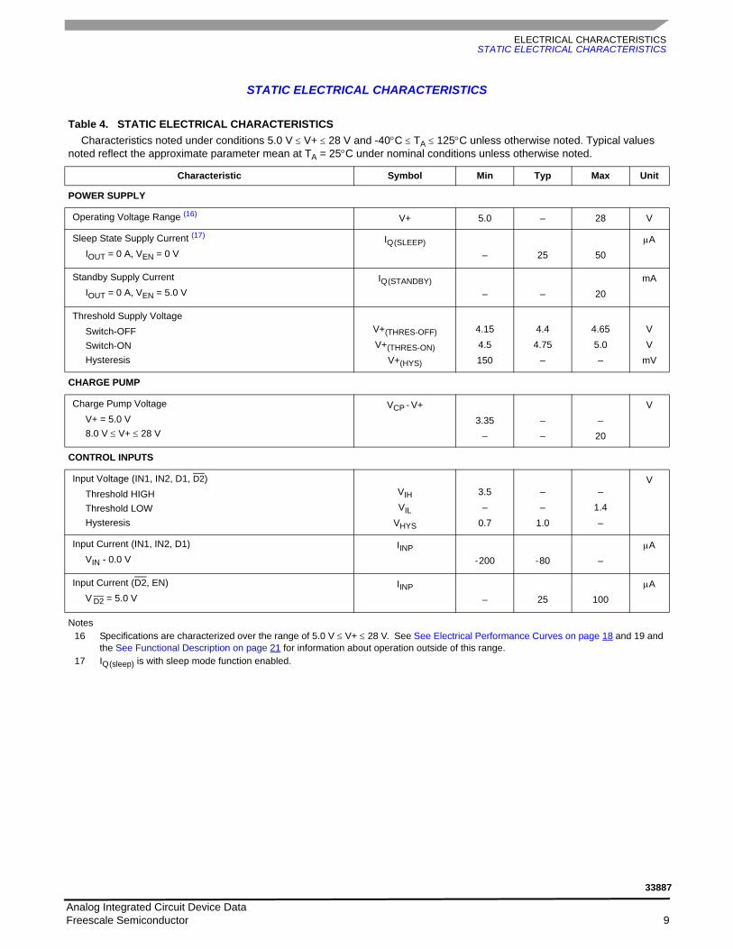
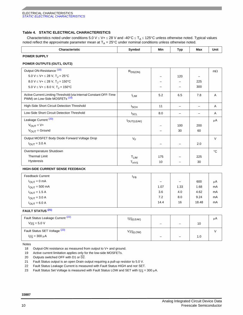
Table 4. STATIC ELECTRICAL CHARACTERISTICSCharacteristics noted under conditions 5.0 V ≤ V+ ≤ 28 V and -40°C ≤ TA ≤ 125°C unless otherwise noted. Typical values
noted reflect the approximate parameter mean at TA = 25°C under nominal conditions unless otherwise noted.
Characteristic Symbol Min Typ Max Unit
POWER SUPPLY
Operating Voltage Range (16) V+ 5.0 – 28 V
Sleep State Supply Current (17)
IOUT = 0 A, VEN = 0 VIQ (SLEEP)
– 25 50µA
Standby Supply CurrentIOUT = 0 A, VEN = 5.0 V
IQ (STANDBY)– – 20
mA
Threshold Supply VoltageSwitch-OFFSwitch-ONHysteresis
V+(THRES-OFF)V+(THRES-ON)
V+(HYS)
4.154.5150
4.44.75
–
4.655.0–
VV
mV
CHARGE PUMP
Charge Pump VoltageV+ = 5.0 V8.0 V ≤ V+ ≤ 28 V
VCP - V+3.35
–––
–20
V
CONTROL INPUTS
Input Voltage (IN1, IN2, D1, D2)Threshold HIGHThreshold LOW Hysteresis
VIHVIL
VHYS
3.5–
0.7
––
1.0
–1.4–
V
Input Current (IN1, IN2, D1)VIN - 0.0 V
IINP- 200 - 80 –
µA
Input Current (D2, EN)V D2 = 5.0 V
IINP– 25 100
µA
Notes16 Specifications are characterized over the range of 5.0 V ≤ V+ ≤ 28 V. See See Electrical Performance Curves on page 18 and 19 and
the See Functional Description on page 21 for information about operation outside of this range.17 IQ (sleep) is with sleep mode function enabled.
Analog Integrated Circuit Device Data Freescale Semiconductor 9
33887
ELECTRICAL CHARACTERISTICSSTATIC ELECTRICAL CHARACTERISTICS
POWER OUTPUTS (OUT1, OUT2)
Output ON-Resistance (18)
5.0 V ≤ V+ ≤ 28 V, TJ = 25°C
8.0 V ≤ V+ ≤ 28 V, TJ = 150°C
5.0 V ≤ V+ ≤ 8.0 V, TJ = 150°C
RDS(ON)–––
120––
–225300
mΩ
Active Current Limiting Threshold (via Internal Constant OFF-Time PWM) on Low-Side MOSFETs (19)
ILIM 5.2 6.5 7.8 A
High-Side Short Circuit Detection Threshold ISCH 11 – – A
Low-Side Short Circuit Detection Threshold ISCL 8.0 – – A
Leakage Current (20)
VOUT = V+
VOUT = Ground
IOUT(LEAK)––
10030
20060
µA
Output MOSFET Body Diode Forward Voltage DropIOUT = 3.0 A
VF– – 2.0
V
Overtemperature ShutdownThermal LimitHysteresis
TLIMTHYS
17510
––
22530
°C
HIGH-SIDE CURRENT SENSE FEEDBACK
Feedback CurrentI OUT = 0 mA
I OUT = 500 mA
I OUT = 1.5 A
I OUT = 3.0 A
I OUT = 6.0 A
I FB–
1.073.67.2
14.4
–1.334.08.016
6001.684.629.24
18.48
µAmAmAmAmA
FAULT STATUS (21)
Fault Status Leakage Current (22)
V FS = 5.0 V I FS(LEAK)
– – 10µA
Fault Status SET Voltage (23)
I FS = 300 µA V FS(LOW)
– – 1.0V
Notes18 Output-ON resistance as measured from output to V+ and ground.19 Active current limitation applies only for the low-side MOSFETs.20 Outputs switched OFF with D1 or D2.21 Fault Status output is an open Drain output requiring a pull-up resistor to 5.0 V.22 Fault Status Leakage Current is measured with Fault Status HIGH and not SET.23 Fault Status Set Voltage is measured with Fault Status LOW and SET with I FS = 300 µA.
Table 4. STATIC ELECTRICAL CHARACTERISTICSCharacteristics noted under conditions 5.0 V ≤ V+ ≤ 28 V and -40°C ≤ TA ≤ 125°C unless otherwise noted. Typical values
noted reflect the approximate parameter mean at TA = 25°C under nominal conditions unless otherwise noted.
Characteristic Symbol Min Typ Max Unit
POWER SUPPLY
Analog Integrated Circuit Device Data 10 Freescale Semiconductor
33887

ELECTRICAL CHARACTERISTICSDYNAMIC ELECTRICAL CHARACTERISTICS
DYNAMIC ELECTRICAL CHARACTERISTICS
Table 5. DYNAMIC ELECTRICAL CHARACTERISTICSCharacteristics noted under conditions 5.0 V ≤ V+ ≤ 28 V and -40°C ≤ TA ≤ 125°C unless otherwise noted. Typical values
noted reflect the approximate parameter mean at TA = 25°C under nominal conditions unless otherwise noted.
Characteristic Symbol Min Typ Max Unit
TIMING CHARACTERISTICS
PWM Frequency (24) f PWM – 10 – kHz
Maximum Switching Frequency During Active Current Limiting (25) f MAX – – 20 kHz
Output ON Delay (26)
V+ = 14 Vt D (ON)
– – 18µs
Output OFF Delay (26)
V+ = 14 Vt D (OFF)
– – 18µs
ILIM Output Constant-OFF Time for Low-Side MOSFETs (27), (28) t A 15 20.5 26 µs
ILIM Blanking Time for Low-Side MOSFETs (29), (28) t B 12 16.5 21 µs
Output Rise and Fall Time (30)
V+ = 14 V, IOUT = 3.0 At F, t R
2.0 5.0 8.0µs
Disable Delay Time (31) t D (DISABLE) – – 8.0 µs
Power-ON Delay Time (32) t POD – 1.0 5.0 ms
Wake-Up Delay Time (32) t WUD – 1.0 5.0 ms
Output MOSFET Body Diode Reverse Recovery Time (33) t R R 100 – – ns
Notes24 The outputs can be PWM-controlled from an external source. This is typically done by holding one input high while applying a PWM
pulse train to the other input. The maximum PWM frequency obtainable is a compromise between switching losses and switching frequency. See Typical Switching Waveforms, Figures 12 through 19, pp. 14–17.
25 The Maximum Switching Frequency during active current limiting is internally implemented. The internal current limit circuitry produces a constant-OFF-time pulse-width modulation of the output current. The output load’s inductance, capacitance, and resistance characteristics affect the total switching period (OFF-time + ON-time) and thus the PWM frequency during current limit.
26 Output Delay is the time duration from the midpoint of the IN1 or IN2 input signal to the 10% or 90% point (dependent on the transition direction) of the OUT1 or OUT2 signal. If the output is transitioning HIGH-to-LOW, the delay is from the midpoint of the input signal to the 90% point of the output response signal. If the output is transitioning LOW-to-HIGH, the delay is from the midpoint of the input signal to the 10% point of the output response signal. See Figure 6, page 12.
27 ILIM Output Constant-OFF Time is the time during which the internal constant-OFF time PWM current regulation circuit has tri-stated the output bridge.
28 Load currents ramping up to the current regulation threshold become limited at the ILIM value. The short circuit currents possess a di/dt that ramps up to the ISCH or ISCL threshold during the ILIM blanking time, registering as a short circuit event detection and causing the shutdown circuitry to force the output into an immediate tri-state latch-OFF. See Figures 10 and 11, page 13. Operation in Current Limit mode may cause junction temperatures to rise. Junction temperatures above ~160°C will cause the output current limit threshold to progressively “fold back”, or decrease with temperature, until ~175°C is reached, after which the TLIM thermal latch-OFF will occur. Permissible operation within this fold-back region is limited to nonrepetitive transient events of duration not to exceed 30 seconds. See Figure 9, page 12.
29 ILIM Blanking Time is the time during which the current regulation threshold is ignored so that the short-circuit detection threshold comparators my have time to act.
30 Rise Time is from the 10% to the 90% level and Fall Time is from the 90% to the 10% level of the output signal. See Figure 8, page 12.31 Disable Delay Time is the time duration from the midpoint of the D (disable) input signal to 10% of the output tri-state response. See
Figure 7, page 12.32 Parameter has been characterized but not production tested.33 Parameter is guaranteed by design but not production tested.
Analog Integrated Circuit Device Data Freescale Semiconductor 11
33887

ELECTRICAL CHARACTERISTICSTIMING DIAGRAMS
TIMING DIAGRAMS
Figure 6. Output Delay Time
Figure 7. Disable Delay Time
Figure 8. Output Switching Time
Figure 9. Active Current Limiting Versus Temperature (Typical)
TIME
0
5.0
0
VPWRtD(ON)
50%
90%
50%
10%
tD(OFF)
∞ Ω
0 V
5.0 V
0 Ω
tR
0
VPWR
90%
10%10%
90%tF
I MAX
,OUT
PUT
CUR
REN
T(A
)
6.6
2.5
160 175
Thermal Shutdown
TJ, JUNCTION TEMPERATURE (oC)
I LIM
,
6.5
I LIM
, CU
RR
EN
T (A
)
4.0
Operation within this region must be
150
limited to nonrepetitive eventsnot to exceed 30 seconds
Analog Integrated Circuit Device Data 12 Freescale Semiconductor
33887
ELECTRICAL CHARACTERISTICSTIMING DIAGRAMS
Figure 10. Operating States
Figure 11. Example Short Circuit Detection Detail on Low-Side MOSFET
ActiveCurrentLimiting
>8A
6.5
Short Circuit Detection Threshold
Typical Current Limit Threshold
Hard Short Detection and Latch-OFF
0
IN1 or IN2
IN2 or IN1
IN1 or IN2
IN2 or IN1IN1 IN2
[1]
[0]
[1]
[0]
[1]
[0]
[1]
[0]
OutputsTri-Stated
OutputsTri-Stated
Outputs Operation(per Input Control Condition)
Time
SF,
LO
GIC
OU
TD
2, L
OG
IC IN
D1,
LO
GIC
ININ
n, L
OG
IC IN
I LO
AD
, OU
TPU
T C
UR
RE
NT
(A)
High Current Load Being Regulated via Constant-OFF-Time PWM
Moderate Current Loadon Low-SideMOSFET
Overcurrent Minimum Threshold
ta tb
8.0
TIME
I LO
AD,O
UTP
UTC
URR
ENT
(A)
Typical PWM LoadCurrent LimitingWaveform
Hard OutputShort Latch-OFF
ta = Tristate Output OFF Timetb = Current Limit Blank Time
6.5
Hard Short Detection
Short Circuit Detect Threshold
ta = Output Constant-OFF Timetb = Output Blanking Time
ISCL Short Circuit Detection Threshold
I OU
T, C
UR
RE
NT
(A)
Typical CurrentLimiting Waveform
tb
5.0
ta
8.0
Hard short occurs. Hard short is detected during tb
ILIM Blanking Timeton
0.0 and output is latched-off.
Analog Integrated Circuit Device Data Freescale Semiconductor 13
33887

ELECTRICAL CHARACTERISTICSTYPICAL SWITCHING WAVEFORMS
TYPICAL SWITCHING WAVEFORMS
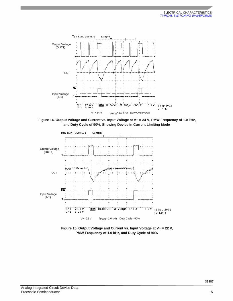
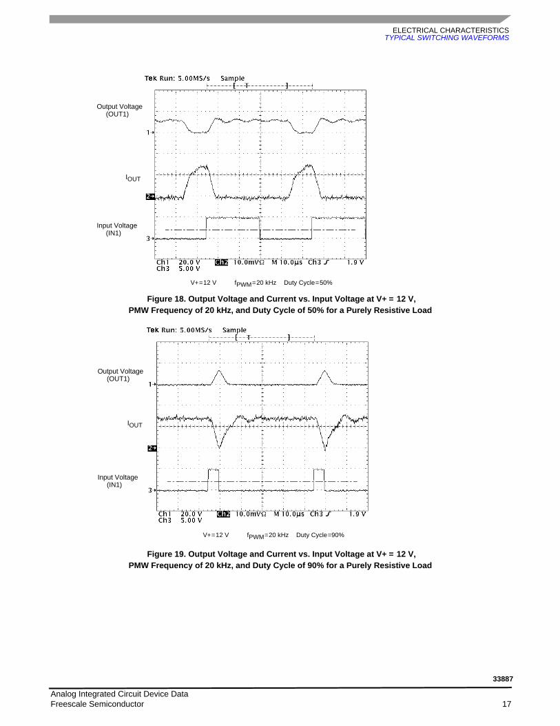
Important For all plots, the following applies:• Ch2 = 2.0 A per division
• LLOAD = 533 µH @ 1.0 kHz• LLOAD = 530 µH @ 10.0 kHz• RLOAD = 4.0 Ω
Figure 12. Output Voltage and Current vs. Input Voltage at V+ = 24 V, PMW Frequency of 1.0 kHz, and Duty Cycle of 10%
Figure 13. Output Voltage and Current vs. Input Voltage at V+ = 24 V, PMW Frequency of 1.0 kHz, and Duty Cycle of 50%
V+=24 V fPWM=1.0 kHz Duty Cycle=10%
Output Voltage(OUT1)
IOUT
Input Voltage (IN1)
V+=24 V fPWM = 1.0 kHz Duty Cycle = 50%
Output Voltage(OUT1)
IOUT
Input Voltage (IN1)
Analog Integrated Circuit Device Data 14 Freescale Semiconductor
33887
ELECTRICAL CHARACTERISTICSTYPICAL SWITCHING WAVEFORMS
Figure 14. Output Voltage and Current vs. Input Voltage at V+ = 34 V, PMW Frequency of 1.0 kHz, and Duty Cycle of 90%, Showing Device in Current Limiting Mode
Figure 15. Output Voltage and Current vs. Input Voltage at V+ = 22 V, PMW Frequency of 1.0 kHz, and Duty Cycle of 90%
V+=34 V fPWM=1.0 kHz Duty Cycle=90%
Output Voltage(OUT1)
IOUT
Input Voltage (IN1)
V+=22 V fPWM=1.0 kHz Duty Cycle=90%
Output Voltage(OUT1)
IOUT
Input Voltage (IN1)
Analog Integrated Circuit Device Data Freescale Semiconductor 15
33887

ELECTRICAL CHARACTERISTICSTYPICAL SWITCHING WAVEFORMS
Figure 16. Output Voltage and Current vs. Input Voltage at V+ = 24 V, PMW Frequency of 10 kHz, and Duty Cycle of 50%
Figure 17. Output Voltage and Current vs. Input Voltage at V+ = 24 V, PMW Frequency of 10 kHz, and Duty Cycle of 90%
V+=24 V fPWM=10 kHz Duty Cycle=50%
Output Voltage(OUT1)
IOUT
Input Voltage(IN1)
V+=24 V fPWM=10 kHz Duty Cycle=90%
Output Voltage(OUT1)
IOUT
Input Voltage(IN1)
Analog Integrated Circuit Device Data 16 Freescale Semiconductor
33887
ELECTRICAL CHARACTERISTICSTYPICAL SWITCHING WAVEFORMS
Figure 18. Output Voltage and Current vs. Input Voltage at V+ = 12 V, PMW Frequency of 20 kHz, and Duty Cycle of 50% for a Purely Resistive Load
Figure 19. Output Voltage and Current vs. Input Voltage at V+ = 12 V, PMW Frequency of 20 kHz, and Duty Cycle of 90% for a Purely Resistive Load
V+=12 V fPWM=20 kHz Duty Cycle=50%
Output Voltage(OUT1)
IOUT
Input Voltage(IN1)
V+=12 V fPWM=20 kHz Duty Cycle=90%
Output Voltage(OUT1)
IOUT
Input Voltage(IN1)
Analog Integrated Circuit Device Data Freescale Semiconductor 17
33887
ELECTRICAL CHARACTERISTICSELECTRICAL PERFORMANCE CURVES
ELECTRICAL PERFORMANCE CURVES
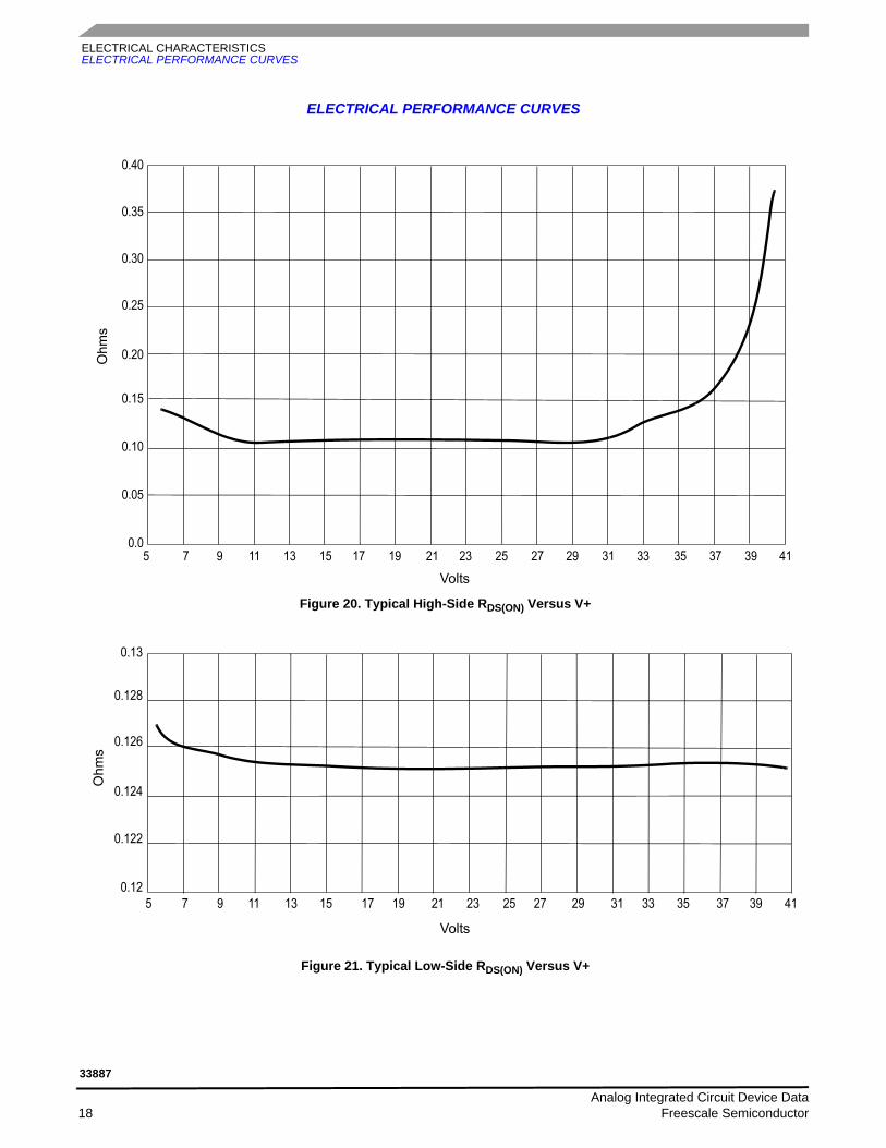
Figure 20. Typical High-Side RDS(ON) Versus V+
Figure 21. Typical Low-Side RDS(ON) Versus V+
2
Analog Integrated Circuit Device Data 18 Freescale Semiconductor
33887
ELECTRICAL CHARACTERISTICSELECTRICAL PERFORMANCE CURVES
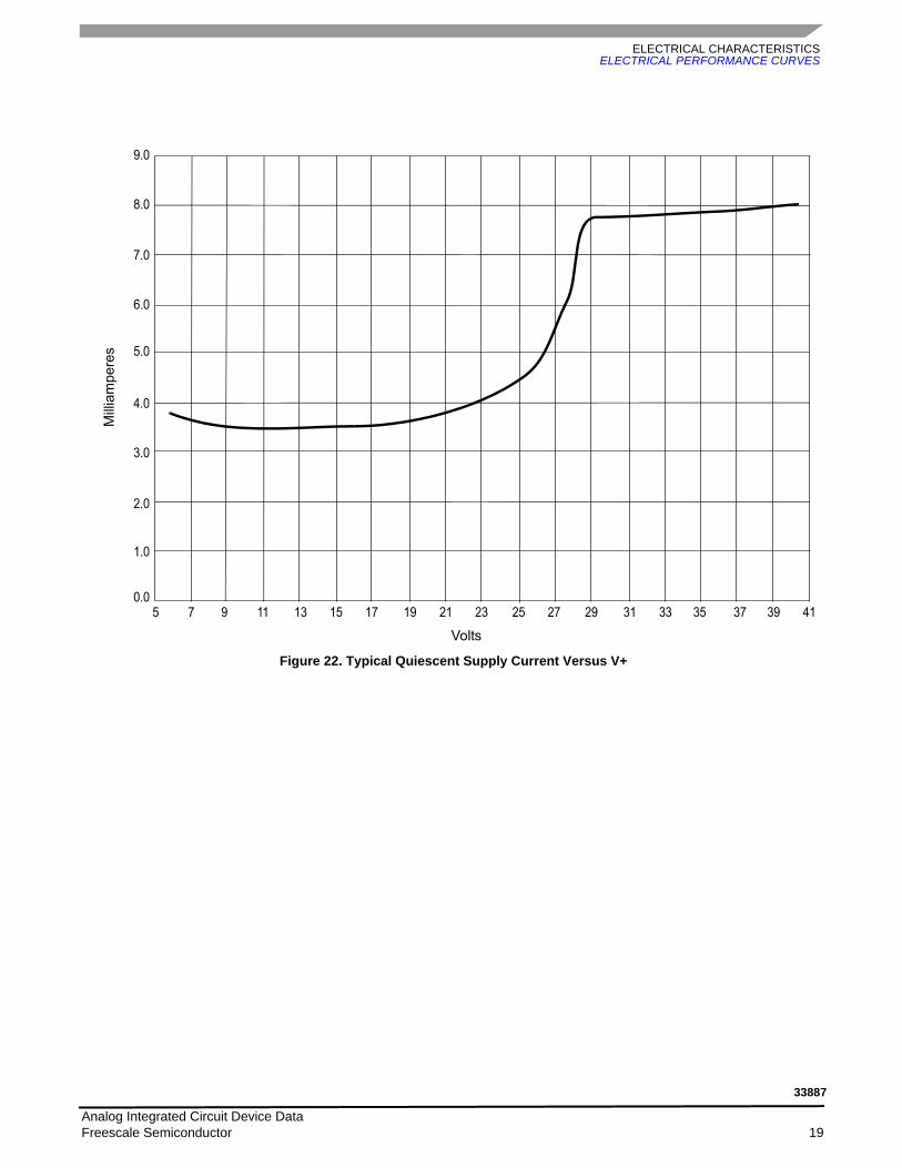
Figure 22. Typical Quiescent Supply Current Versus V+
2
Analog Integrated Circuit Device Data Freescale Semiconductor 19
33887
ELECTRICAL CHARACTERISTICSELECTRICAL PERFORMANCE CURVES
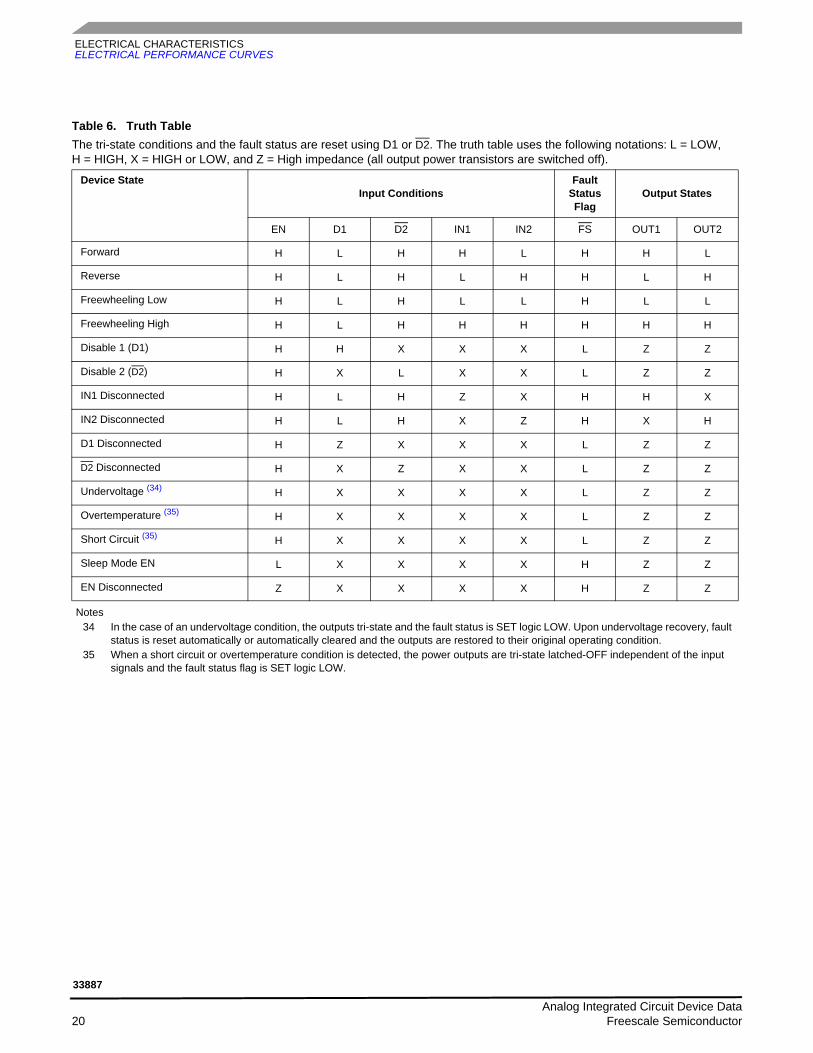
Table 6. Truth TableThe tri-state conditions and the fault status are reset using D1 or D2. The truth table uses the following notations: L = LOW, H = HIGH, X = HIGH or LOW, and Z = High impedance (all output power transistors are switched off).
Device StateInput Conditions
Fault Status Flag
Output States
EN D1 D2 IN1 IN2 FS OUT1 OUT2
Forward H L H H L H H L
Reverse H L H L H H L H
Freewheeling Low H L H L L H L L
Freewheeling High H L H H H H H H
Disable 1 (D1) H H X X X L Z Z
Disable 2 (D2) H X L X X L Z Z
IN1 Disconnected H L H Z X H H X
IN2 Disconnected H L H X Z H X H
D1 Disconnected H Z X X X L Z Z
D2 Disconnected H X Z X X L Z Z
Undervoltage (34) H X X X X L Z Z
Overtemperature (35) H X X X X L Z Z
Short Circuit (35) H X X X X L Z Z
Sleep Mode EN L X X X X H Z Z
EN Disconnected Z X X X X H Z Z
Notes34 In the case of an undervoltage condition, the outputs tri-state and the fault status is SET logic LOW. Upon undervoltage recovery, fault
status is reset automatically or automatically cleared and the outputs are restored to their original operating condition.35 When a short circuit or overtemperature condition is detected, the power outputs are tri-state latched-OFF independent of the input
signals and the fault status flag is SET logic LOW.
Analog Integrated Circuit Device Data 20 Freescale Semiconductor
33887

FUNCTIONAL DESCRIPTIONINTRODUCTION
FUNCTIONAL DESCRIPTION
INTRODUCTION
Numerous protection and operational features (speed, torque, direction, dynamic braking, PWM control, and closed-loop control), in addition to the 5.0 A current capability, make the 33887 a very attractive, cost-effective solution for controlling a broad range of small DC motors. In addition, a
pair of 33887 devices can be used to control bipolar stepper motors. The 33887 can also be used to excite transformer primary windings with a switched square wave to produce secondary winding AC currents.
FUNCTIONAL PIN DESCRIPTIONS
POWER GROUND AND ANALOG GROUND (PGND AND AGND)
Power and analog ground pins should be connected together with a very low impedance connection.
POSITIVE POWER SUPPLY (V+)V+ pins are the power supply inputs to the device. All V+
pins must be connected together on the printed circuit board with as short as possible traces offering as low impedance as possible between pins.
V+ pins have an undervoltage threshold. If the supply voltage drops below a V+ undervoltage threshold, the output power stage switches to a tri-state condition and the fault status flag is SET and the Fault Status pin voltage switched to a logic LOW. When the supply voltage returns to a level that is above the threshold, the power stage automatically resumes normal operation according to the established condition of the input pins and the fault status flag is automatically reset logic HIGH.
As V+ increases in value above 28 V, the charge pump performance begins to degrade. At +40 V, the charge pump is effectively non-functional. Operation at this high voltage level will result in the output FETs not being enhanced when turned on. This means that the voltage on the output will be VOUT = (V+) – VGS. This increased voltage drop under load will produce a higher power dissipation.
FAULT STATUS (FS)The FS pin is the device fault status output. This output is
an active LOW open drain structure requiring a pull-up resistor to 5.0 V. Refer to Table 6, Truth Table, page 20.
LOGIC INPUT CONTROL AND DISABLE (IN1, IN2, D1, AND D2)
These pins are input control pins used to control the outputs. These pins are 5.0 V CMOS-compatible inputs with hysteresis. The IN1 and IN2 independently control OUT1 and OUT2, respectively. D1 and D2 are complementary inputs used to tri-state disable the H-Bridge outputs.
When either D1 or D2 is SET (D1 = logic HIGH or D2 = logic LOW) in the disable state, outputs OUT1 and OUT2 are both tri-state disabled; however, the rest of the circuitry is fully operational and the supply IQ (standby) current is reduced to a
few milliamperes. Refer to Table 6, Truth Table, and STATIC ELECTRICAL CHARACTERISTICS table, page 9.
H-BRIDGE OUTPUT (OUT1 AND OUT2)These pins are the outputs of the H-Bridge with integrated
output MOSFET body diodes. The bridge output is controlled using the IN1, IN2, D1, and D2 inputs. The low-side MOSFETs have active current limiting above the ILIM threshold. The outputs also have thermal shutdown (tri-state latch-OFF) with hysteresis as well as short circuit latch-OFF protection.
A disable timer (time t b) USED to detect currents that are higher than current limit is activated at each output activation to facilitate hard short detection (see Figure 11, page 13).
Charge Pump Capacitor (CCP)A filter capacitor (up to 33 nF) can be connected from the
charge pump output pin and PGND. The device can operate without the external capacitor, although the CCP capacitor helps to reduce noise and allows the device to perform at maximum speed, timing, and PWM frequency.
ENABLE (EN)The EN pin is used to place the device in a sleep mode so
as to consume very low currents. When the EN pin voltage is a logic LOW state, the device is in the sleep mode. The device is enabled and fully operational when the EN pin voltage is logic HIGH. An internal pull-down resistor maintains the device in sleep mode in the event EN is driven through a high impedance I/O or an unpowered microcontroller, or the EN input becomes disconnected.
FEEDBACK FOR H-BRIDGE (FB)The 33887 has a feedback output (FB) for “real time”
monitoring of H-Bridge high-side current to facilitate closed-loop operation for motor speed and torque control.
The FB pin provides current sensing feedback of the H-Bridge high-side drivers. When running in forward or reverse direction, a ground referenced 1/375th (0.00266) of load current is output to this pin. Through an external resistor to ground, the proportional feedback current can be converted to a proportional voltage equivalent and the controlling microcontroller can “read” the current proportional
Analog Integrated Circuit Device Data Freescale Semiconductor 21
33887
FUNCTIONAL DESCRIPTIONFUNCTIONAL PIN DESCRIPTIONS
voltage with its analog-to-digital converter (ADC). This is intended to provide the user with motor current feedback for motor torque control. The resistance range for the linear operation of the FB pin is 100 < RFB < 200 Ω.
If PWM-ing is implemented using the disable pin inputs (either D1 or D2), a small filter capacitor (1.0 µF or less) may be required in parallel with the external resistor to ground for fast spike suppression.
Analog Integrated Circuit Device Data 22 Freescale Semiconductor
33887

FUNCTIONAL DEVICE OPERATIONOPERATIONAL MODES
FUNCTIONAL DEVICE OPERATION
OPERATIONAL MODES
The 33887 Simplified Internal Block Diagram shown in Figure 2, page 2, is a fully protected monolithic H-Bridge with Enable, Fault Status reporting, and High-Side current sense feedback to accommodate closed-loop PWM control. For a DC motor to run, the input conditions need be as follows: Enable input logic HIGH, D1 input logic LOW, D2 input logic HIGH, FS flag cleared (logic HIGH), one IN logic LOW and the other IN logic HIGH (to define output polarity). The 33887 can execute dynamic braking by simultaneously turning on either both high-side MOSFETs or both low-side MOSFETs in the output H-Bridge; e.g., IN1 and IN2 logic HIGH or IN1 and IN2 logic LOW.
The 33887 outputs are capable of providing a continuous DC load current of 5.0 A from a 28 V V+ source. An internal charge pump supports PWM frequencies to 10 kHz. An external pull-up resistor is required at the FS pin for fault status reporting. The 33887 has an analog feedback (current mirror) output pin (the FB pin) that provides a constant-current source ratioed to the active high-side MOSFET. This can be used to provide “real time” monitoring of load current to facilitate closed-loop operation for motor speed/torque control.
Two independent inputs (IN1 and IN2) provide control of the two totem-pole half-bridge outputs. Two disable inputs
(D1 and D2) provide the means to force the H-Bridge outputs to a high-impedance state (all H-Bridge switches OFF). An EN pin controls an enable function that allows the 33887 to be placed in a power-conserving sleep mode.
The 33887 has undervoltage shutdown with automatic recovery, active current limiting, output short-circuit latch-OFF, and overtemperature latch-OFF. An undervoltage shutdown, output short-circuit latch-OFF, or overtemperature latch-OFF fault condition will cause the outputs to turn OFF (i.e., become high impedance or tri-stated) and the fault output flag to be set LOW. Either of the Disable inputs or V+ must be “toggled” to clear the fault flag.
Active current limiting is accomplished by a constant OFF-time PWM method employing active current limiting threshold triggering. The active current limiting scheme is unique in that it incorporates a junction temperature-dependent current limit threshold. This means the active current limiting threshold is “ramped down” as the junction temperature increases above 160°C, until at 175°C the current will have been decreased to about 4.0 A. Above 175°C, the overtemperature shutdown (latch-OFF) occurs. This combination of features allows the device to remain in operation for 30 seconds at junction temperatures above 150°C for nonrepetitive unexpected loads.
Analog Integrated Circuit Device Data Freescale Semiconductor 23
33887
FUNCTIONAL DEVICE OPERATIONPROTECTION AND DIAGNOSTIC FEATURES
PROTECTION AND DIAGNOSTIC FEATURES
SHORT CIRCUIT PROTECTIONIf an output short circuit condition is detected, the power
outputs tri-state (latch-OFF) independent of the input (IN1 and IN2) states, and the fault status output flag is SET logic LOW. If the D1 input changes from logic HIGH to logic LOW, or if the D2 input changes from logic LOW to logic HIGH, the output bridge will become operational again and the fault status flag will be reset (cleared) to a logic HIGH state.
The output stage will always switch into the mode defined by the input pins (IN1, IN2, D1, and D2), provided the device junction temperature is within the specified operating temperature range.
ACTIVE CURRENT LIMITINGThe maximum current flow under normal operating
conditions is internally limited to ILIM (5.2 A to 7.8 A). When the maximum current value is reached, the output stages are tri-stated for a fixed time (t a) of 20 µs typical. Depending on the time constant associated with the load characteristics, the current decreases during the tri-state duration until the next output ON cycle occurs (see Figures 11 and 14, page 13 and page 15, respectively).
The current limiting threshold value is dependent upon the device junction temperature. When -40°C ≤ TJ ≤ 160°C, ILIM is between 5.2 A to 7.8 A. When TJ exceeds 160°C, the ILIM
current decreases linearly down to 4.0 A typical at 175°C. Above 175°C the device overtemperature circuit detects TLIM
and overtemperature shutdown occurs (see Figure 9, page 12). This feature allows the device to remain operational for a longer time but at a regressing output performance level at junction temperatures above 160°C.
Output Avalanche ProtectionAn inductive fly-back event, namely when the outputs are
suddenly disabled and V+ is lost, could result in electrical overstress of the drivers. To prevent this the V+ input to the 33887 should not exceed the maximum rating during a fly-back condition. This may be done with either a zener clamp and/or an appropriately valued input capacitor with sufficiently low ESR.
OVERTEMPERATURE SHUTDOWN AND HYSTERESIS
If an overtemperature condition occurs, the power outputs are tri-stated (latched-OFF) and the fault status flag is SET to logic LOW.
To reset from this condition, D1 must change from logic HIGH to logic LOW, or D2 must change from logic LOW to logic HIGH. When reset, the output stage switches ON again, provided that the junction temperature is now below the overtemperature threshold limit minus the hysteresis.
Note Resetting from the fault condition will clear the fault status flag.
Analog Integrated Circuit Device Data 24 Freescale Semiconductor
33887
TYPICAL APPLICATIONS
TYPICAL APPLICATIONS
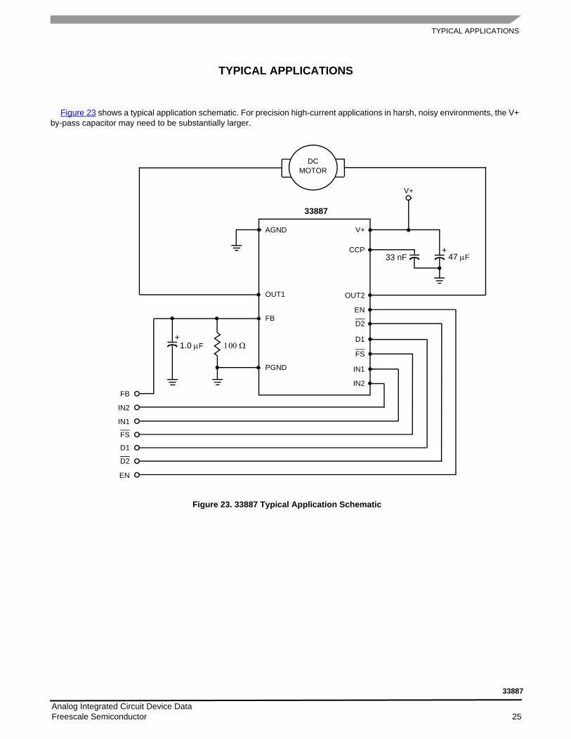
Figure 23 shows a typical application schematic. For precision high-current applications in harsh, noisy environments, the V+ by-pass capacitor may need to be substantially larger.
Figure 23. 33887 Typical Application Schematic
+
+
DCMOTOR
AGND
OUT1
FB
PGND
V+
CCP
OUT2
EN
D2
D1
FS
IN1
IN2
33887
V+
33 nF
1.0 µF 100 Ω
FB
IN2
IN1
FS
D1
EN
D2
47 µF
Analog Integrated Circuit Device Data Freescale Semiconductor 25
33887
PACKAGINGSOLDERING INFORMATION
PACKAGING
SOLDERING INFORMATION
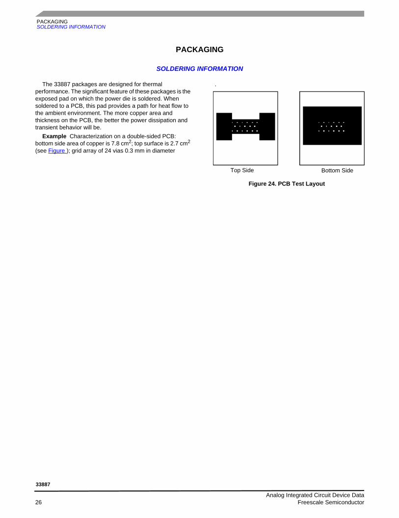
The 33887 packages are designed for thermal performance. The significant feature of these packages is the exposed pad on which the power die is soldered. When soldered to a PCB, this pad provides a path for heat flow to the ambient environment. The more copper area and thickness on the PCB, the better the power dissipation and transient behavior will be.
Example Characterization on a double-sided PCB: bottom side area of copper is 7.8 cm2; top surface is 2.7 cm2 (see Figure ); grid array of 24 vias 0.3 mm in diameter
.
Figure 24. PCB Test Layout
Top Side Bottom Side
Analog Integrated Circuit Device Data 26 Freescale Semiconductor
33887

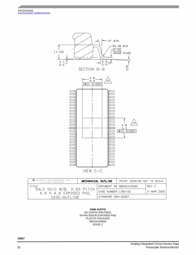
PACKAGINGPACKAGING DIMENSIONS
PACKAGING DIMENSIONS
Important For the most current revision of the package, visit www.freescale.com and perform a keyword search on the 98A drawing number below
DH SUFFIXVW SUFFIX
20-PIN HSOP PLASTIC PACKAGE
98ASH70273AISSUE E
Analog Integrated Circuit Device Data Freescale Semiconductor 27
33887

PACKAGINGPACKAGING DIMENSIONS
DH SUFFIXVW SUFFIX
20-PIN HSOP PLASTIC PACKAGE
98ASH70273AISSUE E
Analog Integrated Circuit Device Data 28 Freescale Semiconductor
33887
PACKAGINGPACKAGING DIMENSIONS
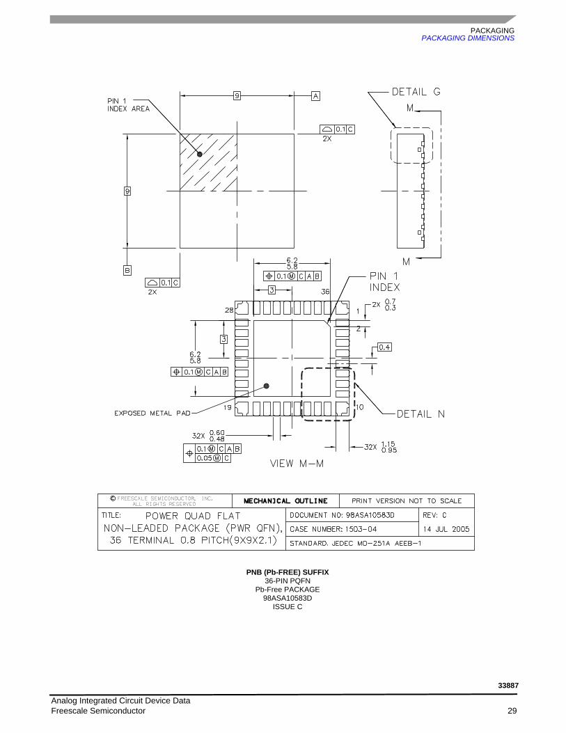
PNB (Pb-FREE) SUFFIX36-PIN PQFN
Pb-Free PACKAGE98ASA10583D
ISSUE C
Analog Integrated Circuit Device Data Freescale Semiconductor 29
33887

PACKAGINGPACKAGING DIMENSIONS
PNB (Pb-FREE) SUFFIX36-PIN PQFN
Pb-Free PACKAGE98ASA10583D
ISSUE C
Analog Integrated Circuit Device Data 30 Freescale Semiconductor
33887

PACKAGINGPACKAGING DIMENSIONS
DWB SUFFIXEK SUFFIX (PB-FREE)
54-PIN SOICW EXPOSED PADPLASTIC PACKAGE
98ASA10506DISSUE C
Analog Integrated Circuit Device Data Freescale Semiconductor 31
33887
PACKAGINGPACKAGING DIMENSIONS
DWB SUFFIXEK SUFFIX (PB-FREE)
54-PIN SOICW EXPOSED PADPLASTIC PACKAGE
98ASA10506DISSUE C
Analog Integrated Circuit Device Data 32 Freescale Semiconductor
33887

ADDITIONAL DOCUMENTATIONTHERMAL ADDENDUM (REV 2.0)
ADDITIONAL DOCUMENTATION
THERMAL ADDENDUM (REV 2.0)
IntroductionThis thermal addendum is provided as a supplement to the MC33887 technical
data sheet. The addendum provides thermal performance information that may be critical in the design and development of system applications. All electrical, application, and packaging information is provided in the data sheet.
Packaging and Thermal ConsiderationsThe MC33887 is offered in a 20 pin HSOP exposed pad, single die package.
There is a single heat source (P), a single junction temperature (TJ), and thermal resistance (RθJA).
The stated values are solely for a thermal performance comparison of one package to another in a standardized environment. This methodology is not meant to and will not predict the performance of a package in an application-specific environment. Stated values were obtained by measurement and simulation according to the standards listed below.
Standards
NOTES:1.Per JEDEC JESD51-2 at natural convection, still air condition.2.2s2p thermal test board per JEDEC JESD51-5 and JESD51-7.3.Per JEDEC JESD51-8, with the board temperature on the center
trace near the center lead.4.Single layer thermal test board per JEDEC JESD51-3 and
JESD51-5.5.Thermal resistance between the die junction and the exposed
pad surface; cold plate attached to the package bottom side, remaining surfaces insulated
Figure 25. Thermal Land Pattern for Direct Thermal Attachment According to JESD51-5
20-PINHSOP-EP
33887DH
Note For package dimensions, refer to the 33887 device data sheet.
DH SUFFIX98ASH70273A
20-PIN HSOP-EPTJ = RθJA . P
Table 7. Thermal Performance Comparison
Thermal Resistance [°C/W]
RθJA(1),(2) 20
RθJB (2),(3) 6.0
RθJA (1), (4) 52
RθJC (5) 1.0
1.0
1.0
0.2
0.2
Soldermastopenings
Thermal viasconnected to topburied plane
* All measurements are in millimeters
20 Terminal HSOP-EP 1.27 mm Pitch 16.0 mm x 11.0 mm Body 12.2 mm x 6.9 mm Exposed Pad
Analog Integrated Circuit Device Data Freescale Semiconductor 33
33887
ADDITIONAL DOCUMENTATIONTHERMAL ADDENDUM (REV 2.0)
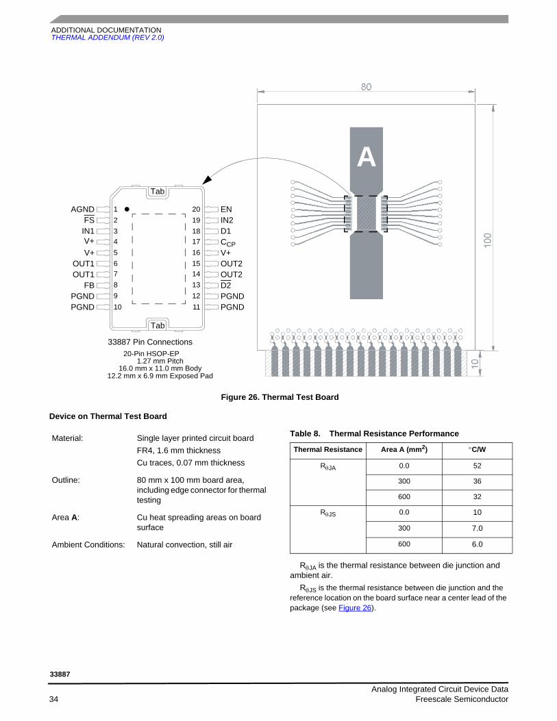
Figure 26. Thermal Test Board
Device on Thermal Test Board
RθJA is the thermal resistance between die junction and ambient air.
RθJS is the thermal resistance between die junction and the reference location on the board surface near a center lead of the package (see Figure 26).
ENAGNDIN2D1CCPV+OUT2OUT2D2PGNDPGND
FS
V+OUT1OUT1
FBPGNDPGND
IN1V+
12345678910
2019
161514131211
1817
Tab
Tab
33887 Pin Connections20-Pin HSOP-EP
1.27 mm Pitch16.0 mm x 11.0 mm Body
12.2 mm x 6.9 mm Exposed Pad
A
Material: Single layer printed circuit boardFR4, 1.6 mm thicknessCu traces, 0.07 mm thickness
Outline: 80 mm x 100 mm board area, including edge connector for thermal testing
Area A: Cu heat spreading areas on board surface
Ambient Conditions: Natural convection, still air
Table 8. Thermal Resistance Performance
Thermal Resistance Area A (mm2) °C/W
RθJA 0.0 52
300 36
600 32
RθJS 0.0 10
300 7.0
600 6.0
Analog Integrated Circuit Device Data 34 Freescale Semiconductor
33887
ADDITIONAL DOCUMENTATIONTHERMAL ADDENDUM (REV 2.0)
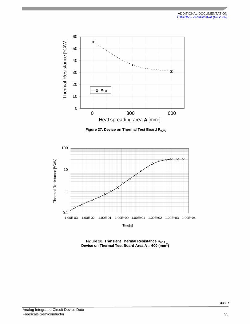
Figure 27. Device on Thermal Test Board RθJA
Figure 28. Transient Thermal Resistance RθJADevice on Thermal Test Board Area A = 600 (mm2)
0
10
20
30
40
50
60
Heat spreading area A [mm²]
Ther
mal
Res
ista
nce
[ºC/W
]
0 300 600
RθJA x
0.1
1
10
100
1.00E-03 1.00E-02 1.00E-01 1.00E+00 1.00E+01 1.00E+02 1.00E+03 1.00E+04
Time[s]
Ther
mal
Res
ista
nce
[ºC/W
]
Analog Integrated Circuit Device Data Freescale Semiconductor 35
33887

REVISION HISTORY
REVISION HISTORY
REVISION DATE DESCRIPTION
10.0 7/2005 • Added Thermal Addendum & Converted to Freescale format, Revised PQFN drawing, made several minor spelling correction. Added 33887A
11.0 11/2006 • Updated Ordering information block with new epp information• Changed the supply/ operating voltage from 40 V to 28 V• Updated all package drawings to the current revision• Adjusted to match device performance characteristics• Updated the document to the prevailing Freescale form and style• Removed Peak Package Reflow Temperature During Reflow (solder reflow) parameter from
Maximum Ratings on page 7. • Added note (8)
• Added MCZ33887EK/R2 to the Ordering Information on Page 1• Removed the 33887A from the data sheet and deleted Product Variation section now that is no
longer needed.
12.0 1/2007 • Changed the third paragraph of the introduction on page 1• Altered feature number 1 on page 1• Added feature number 2 on page 1• Changed Maximum Supply Voltage (1) to 0.3 to 40 V• Added note (1)
• Changed note (16)
• Added a third paragraph to Positive Power Supply (V+) on page 21• Replaced Figure 20, Figure 21, and Figure 22 with updated information.
Analog Integrated Circuit Device Data 36 Freescale Semiconductor
33887

MC33887Rev. 12.02/2007
Information in this document is provided solely to enable system and software implementers to use Freescale Semiconductor products. There are no express or implied copyright licenses granted hereunder to design or fabricate any integrated circuits or integrated circuits based on the information in this document.
Freescale Semiconductor reserves the right to make changes without further notice to any products herein. Freescale Semiconductor makes no warranty, representation or guarantee regarding the suitability of its products for any particular purpose, nor does Freescale Semiconductor assume any liability arising out of the application or use of any product or circuit, and specifically disclaims any and all liability, including without limitation consequential or incidental damages. “Typical” parameters that may be provided in Freescale Semiconductor data sheets and/or specifications can and do vary in different applications and actual performance may vary over time. All operating parameters, including “Typicals”, must be validated for each customer application by customer’s technical experts. Freescale Semiconductor does not convey any license under its patent rights nor the rights of others. Freescale Semiconductor products are not designed, intended, or authorized for use as components in systems intended for surgical implant into the body, or other applications intended to support or sustain life, or for any other application in which the failure of the Freescale Semiconductor product could create a situation where personal injury or death may occur. Should Buyer purchase or use Freescale Semiconductor products for any such unintended or unauthorized application, Buyer shall indemnify and hold Freescale Semiconductor and its officers, employees, subsidiaries, affiliates, and distributors harmless against all claims, costs, damages, and expenses, and reasonable attorney fees arising out of, directly or indirectly, any claim of personal injury or death associated with such unintended or unauthorized use, even if such claim alleges that Freescale Semiconductor was negligent regarding the design or manufacture of the part.
Freescale™ and the Freescale logo are trademarks of Freescale Semiconductor, Inc. All other product or service names are the property of their respective owners.© Freescale Semiconductor, Inc., 2007. All rights reserved.
RoHS-compliant and/or Pb-free versions of Freescale products have the functionality and electrical characteristics of their non-RoHS-compliant and/or non-Pb-free counterparts. For further information, see http://www.freescale.com or contact your Freescale sales representative.
For information on Freescale’s Environmental Products program, go to http://www.freescale.com/epp.
How to Reach Us:
Home Page:www.freescale.com
Web Support:http://www.freescale.com/support
USA/Europe or Locations Not Listed:Freescale Semiconductor, Inc.Technical Information Center, EL5162100 East Elliot Road Tempe, Arizona 85284 +1-800-521-6274 or +1-480-768-2130www.freescale.com/support
Europe, Middle East, and Africa:Freescale Halbleiter Deutschland GmbHTechnical Information CenterSchatzbogen 781829 Muenchen, Germany+44 1296 380 456 (English)+46 8 52200080 (English)+49 89 92103 559 (German)+33 1 69 35 48 48 (French)www.freescale.com/support
Japan:Freescale Semiconductor Japan Ltd. Headquarters ARCO Tower 15F 1-8-1, Shimo-Meguro, Meguro-ku, Tokyo 153-0064Japan0120 191014 or +81 3 5437 [email protected]
Asia/Pacific:Freescale Semiconductor Hong Kong Ltd.Technical Information Center 2 Dai King Street Tai Po Industrial Estate Tai Po, N.T., Hong Kong +800 2666 [email protected]
For Literature Requests Only:Freescale Semiconductor Literature Distribution CenterP.O. Box 5405Denver, Colorado 802171-800-441-2447 or 303-675-2140Fax: [email protected]