manufacturing process and design rules - electrical and …€¦ · · 2016-02-09manufacturing...
TRANSCRIPT

520.216 1 1
Andreas G. Andreou Pedro Julian Electrical and Computer Engineering Johns Hopkins University http://andreoulab.net
Manufacturing process and design rules

Levels of Abstraction –the CMOS Inverter-
Introduction to VLSI Systems 2
Layout
DEEP SUBMICRON CMOS DESIGN 4. The inverter
1 E.Sicard, S. Delmas-Bendhia 20/12/03
4 The Inverter
The inverter is probably the most important basic logic cell in circuit design. This chapter introduces the logical
concepts of the inverter, its layout implementation, the link between the transistor size and the static and analog
characteristics. The manual design of the inverter is detailed. The performances of the inverter are analyzed in terms of
static transfer function, switching speed, MOS options influence, and power consumption.
1. Logic symbol
Two logic symbols are often used to represent the inverter: the "old style" inverter (Left of figure 4-1), and the IEEE
symbol (right of figure 4-1). In DSCH, we preferably use traditional symbol layout. As the logic truth table of figure 4-
1 shows, the cell inverts the logic value of the input In into an output Out.
In Out
0 1
1 0
X X
Fig. 4-1: Symbols used to represent the logic inverter
In the truth table, the symbol 0 represents 0.0V while 1 represents the logic supply, which is 1.2V in 0.12µm. The
symbol X means "undefined". This state is equivalent to an undefined voltage, just like with a floating input node
without any input connection. The undefined state appears in gray in the simulations and chronograms.
Symbol
PHYSICAL LOGICAL
Out = NOT (In) Out = ~ (In)
Equation
DEEP SUBMICRON CMOS DESIGN 4. The inverter
1 E.Sicard, S. Delmas-Bendhia 20/12/03
4 The Inverter
The inverter is probably the most important basic logic cell in circuit design. This chapter introduces the logical
concepts of the inverter, its layout implementation, the link between the transistor size and the static and analog
characteristics. The manual design of the inverter is detailed. The performances of the inverter are analyzed in terms of
static transfer function, switching speed, MOS options influence, and power consumption.
1. Logic symbol
Two logic symbols are often used to represent the inverter: the "old style" inverter (Left of figure 4-1), and the IEEE
symbol (right of figure 4-1). In DSCH, we preferably use traditional symbol layout. As the logic truth table of figure 4-
1 shows, the cell inverts the logic value of the input In into an output Out.
In Out
0 1
1 0
X X
Fig. 4-1: Symbols used to represent the logic inverter
In the truth table, the symbol 0 represents 0.0V while 1 represents the logic supply, which is 1.2V in 0.12µm. The
symbol X means "undefined". This state is equivalent to an undefined voltage, just like with a floating input node
without any input connection. The undefined state appears in gray in the simulations and chronograms.
Truth Table
Circuit
Voltage Transfer Characteristics (VTC)
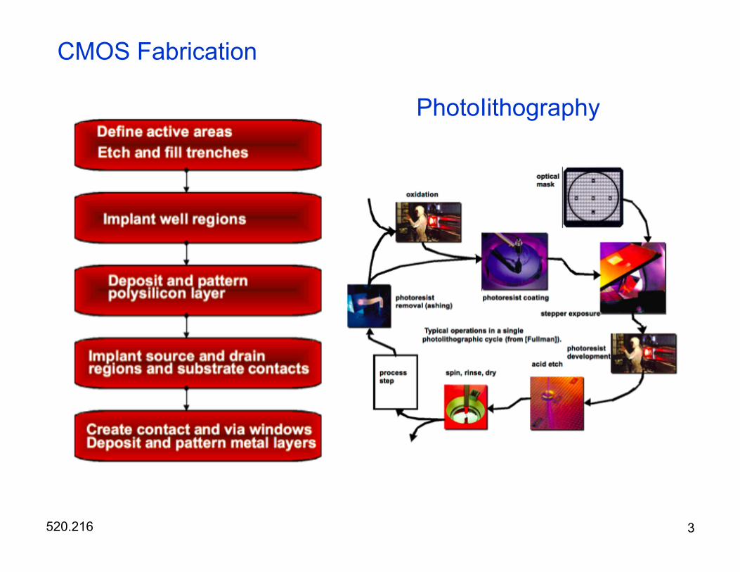
CMOS Fabrication
520.216 3
PhotoIithography

Patterning of silicon dioxide
520.216 4

Designing an inverter
520.216 5
520.216 6
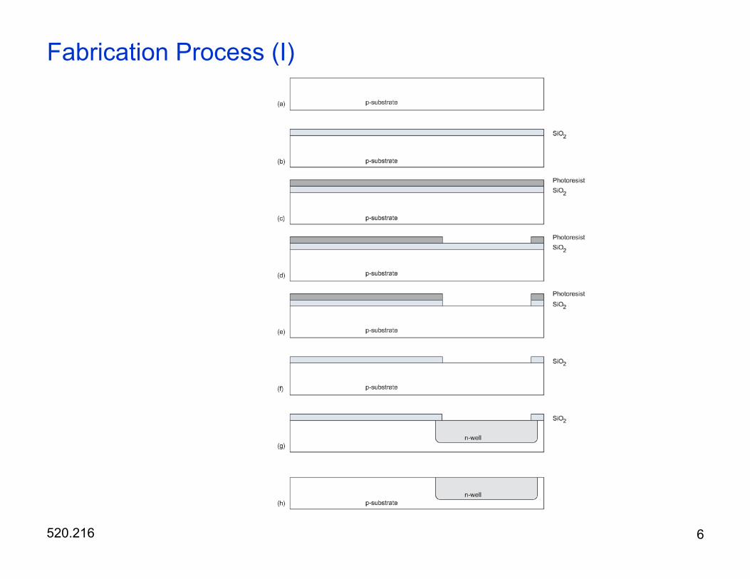
Fabrication Process (I)

520.216 7
Fabrication Process (II)

Process cross-section
520.216 8

Design Rules
520.216 9
• The interface between the design engineer (you!) and the process engineer (the guys in the white space suits!)
• Guidelines for constructing masks (constraints)
• Dimensions: • Dimensionless (lambda parameter) • Absolute (nanometer)
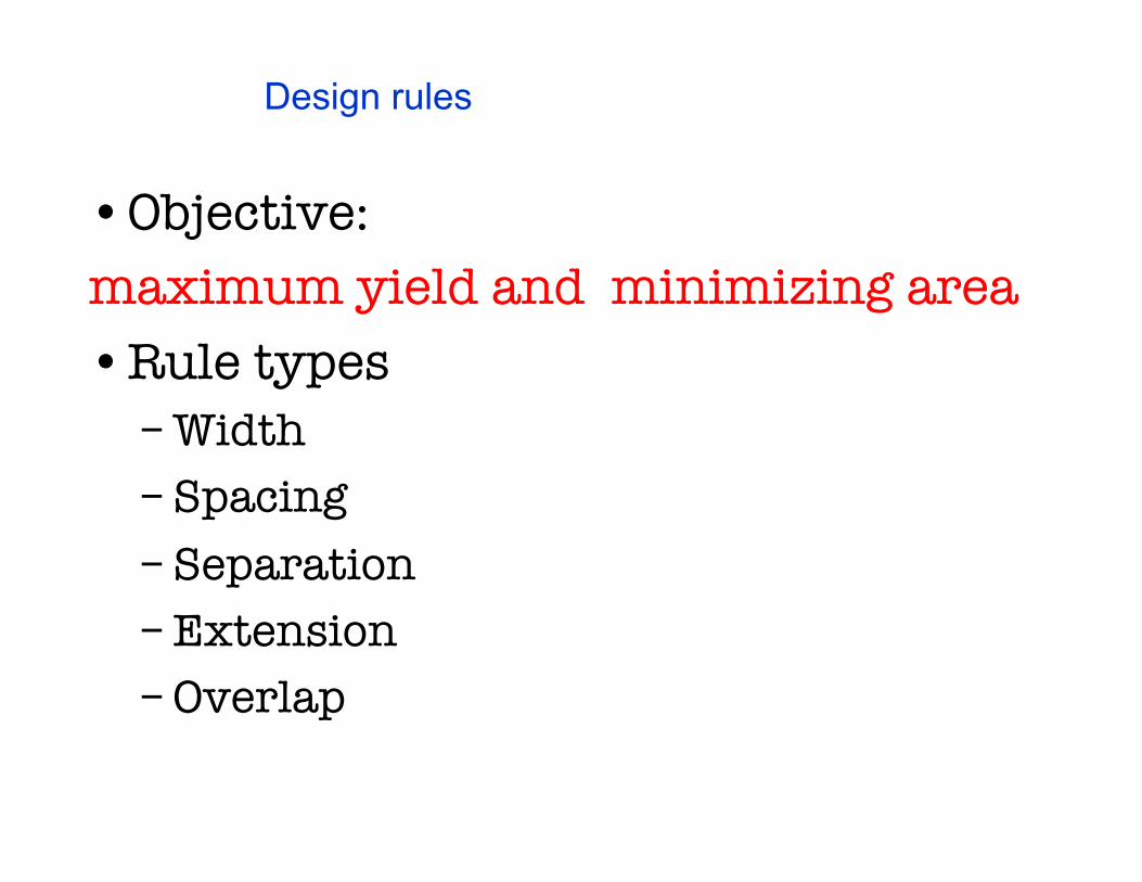
• Objective: maximum yield and minimizing area • Rule types
– Width – Spacing – Separation – Extension – Overlap
Design rules

Design Rules (I)
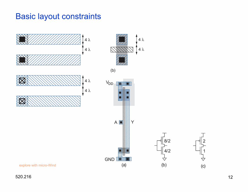
Basic layout constraints
520.216 12
explore with micro-Wind

Layout style for libraries –stick diagrams- (I)
520.216 13
explore with micro-Wind
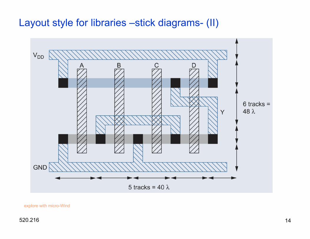
Layout style for libraries –stick diagrams- (II)
520.216 14
explore with micro-Wind

Substrate and well contact –the fourth hidden terminal-
520.216 15
explore with micro-Wind
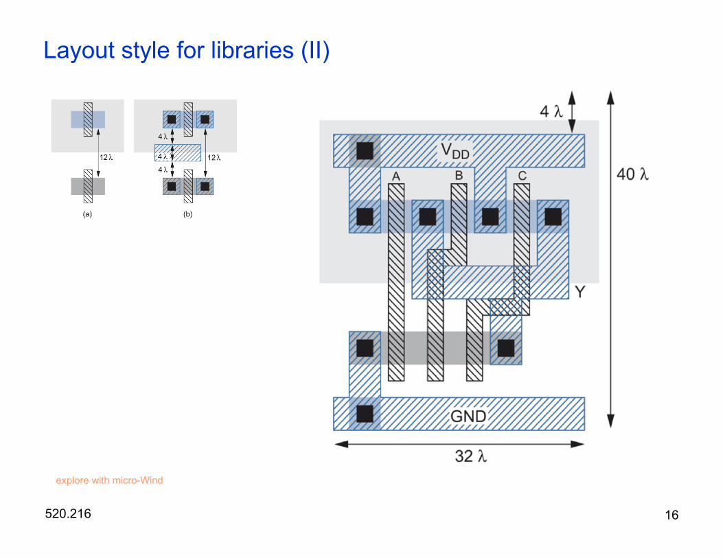
Layout style for libraries (II)
520.216 16
explore with micro-Wind

Computer Aided Design Tools
520.216 17
MICROWIND Tool Design Flow
Contact: Sales : [email protected] Support : [email protected]
SPICE Simulator (3rd Party)
Schematic Modeling Analog & digital Library models
Digital Simulation SPICE Extraction
DSCH 3
Tape out to FAB. CIF
Functional Simulation
Floorplanning
Place & Route
Programming File
.bit or .jed
IO Cards Traffic Light Controller, Key Pad, Display (LCD, 7 segs)
Synthesis
ModelSim / other
ProTHUMB Advance post layout
simulator
Analysis DRC, ERC
Delay Analyzer Crosstalk Analyzer 2D Cross section
3D Analyzer
Layout Conversion SPICE, CIF
Constraints
Technology rule files
MICROWIND 3
Verilog Extraction
Verilog File
nanoLambda Layout Editor
Verilog Compiler
Place & Route
Layout Extraction
FPGA / CPLD Boards
FPGA Tools
MICROWIND Tool
3rd Party Tools
LTSpice WindSpice
http://www.microwind.net