manual - madhurikawade.files.wordpress.com · using shift register ic 74194. group c vhdl...
TRANSCRIPT

Department of Information Technology Digital Laboratory
SNJBrsquos LS KBJrsquos COEChandwad 1 85
SNJBrsquos Late Sau K B Jain College of Engineering Chandwad
Department Information Technology
2018-2019
Lab Instructorrsquos
Manual
Name of Faculty Kawade Madhuri D
Subject DIGITAL LABORATORY Code 214446
SEIT (2015 Course) Semester I
Teaching Scheme- Examination Scheme
Practical 2 HrsWeek TW 25 Marks
Theory 4 HrsWeek Practical 50 Marks
Department of Information Technology Digital Laboratory
SNJBrsquos LS KBJrsquos COEChandwad 2 85
PREFACE
Every day digital concepts are being applied to problems that could only be solved by analog
methods several years ago Fast and reliable solutions using digital techniques proved the
tremendous power and usefulness of digital electronics Nowadays digital circuits are used in
wide variety of industrial and consumer products such as automated industrial machinery
pocket calculators digital computers digital watches and TV games
This laboratory deals with the basic understanding of the digital electronics and provides
thorough understanding of principles and design of digital applications
In the next stage of the manual hardware description language programming is discussed
VHDL is a hardware description language that can be used to model a digital system It contains
elements that can be used to describe the behavior or structure of the digital system with the
provision for specifying its timing explicitly Emphasis is placed on providing illustrative
examples that explain the different formulations of the language constructs and their semantics
In Digital laboratory theory comes alive and practical hands-on skills are learnt a balance is
struck between theory and practice
This laboratory manual is prepared by referring to various standard books which help the
students to perform the experiments Students are not expected to copy the contents of the
manual as it is They must understand the concepts given in the manual and write journal on
their own The manual is prepared as per Pune University syllabus and accordingly the practical
assignments are discussed in the manual However students can go beyond this set and perform
extra practical assignments
Department of Information Technology Digital Laboratory
SNJBrsquos LS KBJrsquos COEChandwad 3 85
University Syllabus
214446 DIGITAL LABORATORY
Teaching Scheme Credits 01 Examination scheme
Practical 2hrs week Practical 50 Marks
TW 25 Marks
Group A
Combinational Logic Design
1 Design (truth table K-map) and implementation of 4-bit BCD to Excess-3 and Excess-3 to
BCD Code converters
2 Design (truth table K-map) and implementation of 4 bit BCD amp Excess 3 Adder
using IC7483
3 Implementation of logic functions using multiplexer IC 74153 amp decoder IC
74138 (Verification cascading amp logic function implementation)
Group B
Sequential Logic Design
1 Design (State diagram state table amp K map) and implementation of 3 bit Up and Down
Asynchronous and Synchronous Counter using master slave JK flip-flop IC 7476
2 Design and implementation of Module lsquonrsquo counter with IC7490 and IC 74191
3 Design (State Diagram State Table K Map) and implementation of Sequence Generator
using Shift Register IC 74194
Group C
VHDL Programming
Simulation of
1 41 multiplexer using data flow amp structural modeling
2 Full adder using behavioral amp structural modeling
3 3 bit controlled up down synchronous counter with preset amp clear
Group D
Design construct digital logic circuits amp analyze their behavior through simulation of any one
assignment from either group A or Group B with simulation software like Digital works 30
Reference Books
1 Modern Digital Electronics RP Jain 3rd EditionTata McGraw-Hill ISBN 0-07-
049492-4
2 Fundamentals of Digital Logic with VHDL Design Stephen Brown ZvonkoVranesic
McGraw-Hill ISBN 978-0-07-352953-0
Department of Information Technology Digital Laboratory
SNJBrsquos LS KBJrsquos COEChandwad 4 85
3 Digital Logic applications and Design John Yarbrough Thomson PublicationISBN
978-0314066756
Instructor will frame assignments based on the suggested assignments as given above Students
will submit the term work in the form of journal consisting of 9 assignments listed above
Practical examination will be based on practical assignments and questions will be asked to
judge the understanding of assignments performed at the time of examination
Note - Instructor should take care that datasheets of all the required ICs are available in
the laboratory amp students are verifying the functionality of ICs being used
INDEX
Sr
No Title
Page No
Group A Combinational circuit design
1 Design amp implement 4 bit Code Converterhelliphelliphelliphelliphelliphelliphelliphelliphelliphelliphelliphelliphelliphellip 1
a BCD to Excess-3
b Excess-3 to BCD
2 Design amp implement BCD amp Excess 3 Adder using IC 7483helliphelliphellip 11
BCD amp Excess 3 Adder using IC 7483(4 bit binary adder)
3 Implementation of logic functions using multiplexer IC 74153 amp decoder IC
74138
18
(Verification cascading amp logic function implementation)
Group B Sequential Logic Design
4 Design amp implement 3 bit Asynchronous amp Synchronous counter 28
a 3 bit up Asynchronous counter
b 3 bit down Asynchronous counter
c 3 bit up Synchronous counter
d 3 bit down Synchronous counter
5 Design amp implement Modulus- N counterhelliphelliphelliphelliphelliphelliphelliphelliphelliphelliphelliphelliphelliphelliphellip 40
a Using IC 7490 (BCD counter)
b Using IC 74191 (Binary counter)
6 Design amp implement sequence generator using shift register IC 74194 54
Group C VHDL Programming amp simulation
7 Simulation of 41 mux helliphelliphelliphelliphelliphelliphelliphelliphelliphelliphelliphelliphelliphelliphelliphelliphelliphelliphelliphelliphelliphellip 61
a Using data flow modeling
b Using structural modeling
8 Simulation of Full Adderhelliphelliphelliphelliphelliphelliphelliphelliphelliphelliphelliphelliphelliphelliphelliphelliphelliphelliphelliphelliphellip 66
a Using behavioral modeling
b Using structural modeling
9 Simulation of 3 bit controlled updown Synchronous counter with preset amp clear 72
a Using data flow modeling
b Using behavioral modeling
Regularity Content Viva-voce Timely
Submission Total
Dated Sign of
Subject
Teacher
2 4 2 2 10
Date of Performance Date of Completion
-------------------------------------------------------------------------------------------------------------------
Assignment No 1
-------------------------------------------------------------------------------------------------------------------------------
Title Code Converter
------------------------------------------------------------------------------------------------------------------
Objective To learn and understand design and construction of combination circuit BCD to Excess-3
and Excess-3 to BCD code convertor
-------------------------------------------------------------------------------------------------------------------
Problem Statement Design (truth table K-map) and implementation of 4-bitBCD to Excess-3
and Excess-3 to BCD Code converters
-----------------------------------------------------------------------------------------------------------------
Hardware Requirement
i) IC 7404(Not-gate) 7432 (OR-gate) 7408 (AND-gate) 7486 (Ex-or gate)
ii) Digital Trainer Kit -1
iii) Patch cords
----------------------------------------------------------------------------------------------------------------
Software Requirement Digital Work 30
Theory
Introduction There is a wide variety of binary codes used in digital systems Some of these codes are
binary- coded -decimal (BCD) Excess-3 Gray octal hexadecimal etc Often it is required to convert
from one code to another For example the input to a digital system may be in natural BCD and output
may be 7-segment LEDs The digital system used may be capable of processing the data in straight binary
format Therefore the data has to be converted from one type of code to another type for different
purpose The various code converters can be designed using gates
Department of Information Technology Digital Laboratory
1
1 BCD Code
Binary Coded Decimal (BCD) is used to represent each of decimal digits (0 to 9) with a 4-bit binary code
For example (23)10 is represented by 0010 0011 using BCD code rather than(10111)2 This code is also
known as 8-4-2-1 code as 8421 indicates the binary weights of four bits(23 22 21 20) It is easy to convert
between BCD code numbers and the familiar decimal numbers It is the main advantage of this code With
four bits sixteen numbers (0000 to 1111) can be represented but in BCD code only 10 of these are used
The six code combinations (1010 to 1111) are not used and are invalid
Applications Some early computers processed BCD numbers Arithmetic operations can be performed
using this code Input to a digital system may be in natural BCD and output may be 7-segment LEDs
It is observed that more number of bits are required to code a decimal number using BCD code than using
the straight binary code However in spite of this disadvantage it is very convenient and useful code for
input and output operations in digital systems
Fig 1 BCD Coded Decimal Representation
2 EXCESS-3 Code
Excess-3 also called XS3 is a non-weighted code used to express decimal numbers It can be used for the
representation of multi-digit decimal numbers as can BCDThe code for each decimal number is obtained
by adding decimal 3 and then converting it to a 4-bit binary number For eg decimal 2 is coded as 0010 +
0011 = 0101 in Excess-3 code
This is self-complementing code which means 1rsquos complement of the coded number yields 9rsquos
complement of the number itself Self-complementing property of this helps considerably in performing
subtraction operation in digital systems so this code is used for certain arithmetic operations
Department of Information Technology Digital Laboratory
2
BCD To Excess ndash 3 Code Conversions
Convert BCD 2 i e 0010 to Excess ndash 3 code
For converting 4 bit BCD code to Excess ndash 3 add 0011 i e decimal 3 to the respective code using rules of
binary addition
0010 + 0011 = 0101 ndash Excess ndash 3 code for BCD 2
Excess ndash 3 Code To BCD Conversion
The 4 bit Excess-3 coded digit can be converted into BCD code by subtracting decimal value 3 ie 0011
from 4 bit Excess-3 digit
eg Convert 4-bit Excess-3 value 0101 to equivalent BCD code
0101-0011= 0010- BCD for 2
A BCD To Excess-3 Code Conversion
Step 1 Truth Table
INPUT (BCD CODE) OUTPUT (EXCESS-3 CODE)
B3 B2 B1 B0 E3 E2 E1 E0
0 0 0 0 0 0 1 1
0 0 0 1 0 1 0 0
0 0 1 0 0 1 0 1
0 0 1 1 0 1 1 0
0 1 0 0 0 1 1 1
0 1 0 1 1 0 0 0
0 1 1 0 1 0 0 1
0 1 1 1 1 0 1 0
1 0 0 0 1 0 1 1
1 0 0 1 1 1 0 0
Department of Information Technology Digital Laboratory
3
Step 2 K-Map For Reduced Boolean Expressions Of Each Output
Fig 2 K-Map for Reduced Boolean Expressions Of Each Output (Excess-3 Code)
Department of Information Technology Digital Laboratory
4
Step3 Circuit Diagram Test the circuit for all possible combinations of input and output codes
4) Hardware Requirements Table
Table 1 Hardware Requirement Table
GATE Quantity
IC Quantity
XOR 1 7486 1
NOT 4 7404 1
AND 4 7408 1
OR 3 7432 1
Department of Information Technology Digital Laboratory
5
B Excess-3 To BCD Conversion
1 Truth Table
INPUT (EXCESS-3 CODE) OUTPUT (BCD CODE)
E3 E2 E1 E0 B3 B2 B1 B0
0 0 0 0 X X X X
0 0 0 1 X X X X
0 0 1 0 X X X X
0 0 1 1 0 0 0 0
0 1 0 0 0 0 0 1
0 1 0 1 0 0 1 01O6
51
0 1 1 0 0 0 1 1
0 1 1 1 0 1 0 0
1 0 0 0 0 1 0 1
1 0 0 1 0 1 1 0
1 0 1 0 0 1 1 1
1 0 1 1 1 0 0 0
1 1 0 0 1 0 0 1
1 1 0 1 X X X X
1 1 1 0 X X X X
1 1 1 1 X X X X
Department of Information Technology Digital Laboratory
6
2) K-Map For Reduced Boolean Expressions Of Each Output
Fig 5 K-Map For Reduced Boolean Expressions Of Each Output (BCD Code)
Department of Information Technology Digital Laboratory
7
3) Circuit Diagram Test the circuit for all possible combinations of input and output codes
4) Hardware Requirements Table
Table 2 Hardware Requirement Table
GATE Quantity
IC Quantity
XOR 1 7486 1
NOT 3 7404 1
AND 8 7408 2
OR 3 7432 1
Pin Diagrams
Department of Information Technology Digital Laboratory
8
7400 Quad 2-Input NAND Gate
7402 Quad 2-Input NOR Gate
7404 Not Gates
7408 Quad 2-Input AND Gates
7432 Quad 2-Input OR Gate
7486 Quad 2-Input Exclusive-OR Gate
Department of Information Technology Digital Laboratory
9
Conclusion
Thus we studied different codes and their conversions including applications
The truth tables have been verified using IC 7486 7432 7408 and 7404
FAQrsquos with answers
Q1) What is the need of code converters
There is a wide variety of binary codes used in digital systems Often it is required to convert from one
code to another For example the input to a digital system may be in natural BCD and output may be 7-
segment LEDs The digital system used may be capable of processing the data in straight binary format
Therefore the data has to be converted from one type of code to another type for different purpose
Q2) What is Gray code
It is a modified binary code in which a decimal number is represented in binary form in such a way that
each Gray- Code number differs from the preceding and the succeeding number by a single bit
(eg for decimal number 5 the equivalent Gray code is 0111 and for 6 it is 0101 These two codes differ
by only one bit position i e third from the left) It is non weighted code
Q3) What is the significance of Gray code
Important feature of Gray code is it exhibits only a single bit change from one code word to the next in
sequence Whereas by using binary code there is a possibility of change of all bits if we move from one
number to other in sequence (eg binary code for 7 is 0111 and for 8 it is 1000) Therefore it is more
useful to use Gray code in some applications than binary code
Q4) What are applications of Gray code
1 Important feature of Gray code is it exhibits only a single bit change from one code word to the next in
sequence This property is important in many applications such as Shaft encoders where error
susceptibility increases with number of bit changes between adjacent numbers in sequence
2 It is sometimes convenient to use the Gray code to represent the digital data converted from the analog
data (Outputs of ADC)
3 Gray codes are used in angle-measuring devices in preference to straight forward binary encoding
Department of Information Technology Digital Laboratory
10
4 Gray codes are widely used in K-map
Q5) What are weighted codes and non-weighted codes
In weighted codes each digit position of number represents a specific weight The codes 8421 2421 and
5211 are weighted codes Non weighted codes are not assigned with any weight to each digit position ie
each digit position within the number is not assigned a fixed value Gray code Excess-3 code are non-
weighted code
Q6) Why is Excess-3 code called as self-complementing code
Excess-3 code is called self-complementing code because 9rsquos complement of a coded number can be
obtained by just complementing each bit
Q7) What is invalid BCD
With four bits sixteen numbers (0000 to 1111) can be represented but in BCD code only 10 of these are
used as decimal numbers have only 10 digits fro 0 to 9 The six code combinations (1010 to 1111) are not
used and are invalid
Department of Information Technology Digital Laboratory
11
Regularity Content Viva-voce Timely
Submission Total
Dated Sign of
Subject
Teacher
2 4 2 2 10
Date of Performance Date of Completion
-------------------------------------------------------------------------------------------------------------------
Assignment No 2
------------------------------------------------------------------------------------------------------------------
Title BCD amp Excess 3 Adder
------------------------------------------------------------------------------------------------------------------
Objective 1 To study the BCD arithmetic rules
2 Comparison between binary and BCD codes
Problem Statement Design (truth table K-map) and implementation of 4-bit BCD to Excess-3 and
Excess-3 to BCD Code converters
-----------------------------------------------------------------------------------------------------------------
Hardware Requirement
i) IC 7483 (4 bit Binary adder) IC 7404(Hex INV) 7432 (OR-gate) 7408 (AND-gate)
ii) 7486 (EX-OR gate)
iii) Digital Trainer Kit -1
iv) Patch cords
----------------------------------------------------------------------------------------------------------------
Software Requirement Digital Work 30
------------------------------------------------------------------------------------------------------------------
Theory
BCD-Binary coded decimal-In this code each decimal digit represent by a 4-bit binary no BCD is a
way to express each of the decimal digits with binary code Positional weights associated to the binary bits
in BCD code are (MSB) 8-4-2-1(LSB)
BCD number 0 to 9 but greater than 9 is invalid BCD
Department of Information Technology Digital Laboratory
12
So Convert in valid BCD using add 6 ie (0110)
BCD Adder
BCD adder is a circuit that adds two BCD digits amp produces a sum of digits also in BCD
Rules for BCD addition
1 Add two numbers using rules of Binary addition
2 If the 4 bit sum is greater than 9 or if carry is generated then the sum is invalid To correct the sum
add 0110 i e (6)10 to sum If carry is generated from this addition add it to next higher order BCD
digit
3 If the 4 bit sum is less than 9 or equal to 9 then sum is in proper form
CASE I Sum lt= 9 amp carry = 0
Add BCD digits 3 amp 4
1 0 0 1 1
+ 0 1 0 0
------------
0 1 1 1
Answer is valid BCD number = (7)BCDamp so 0110 is not added
CASE II Sum gt 9 amp carry = 0
Add BCD digits 6 amp 5
1 0 1 1 0
+ 0 1 0 1
-----------
10 1 1
Department of Information Technology Digital Laboratory
13
Invalid BCD (since sum gt 9) so 0110 is to be added
2 1 0 1 1
+ 0 1 1 0
-----------
1 0 0 0 1
(1 1)BCD
Valid BCD result = (11) BCD
CASE III Sum lt = 9 amp carry = 1
Add BCD digits 9 amp 9
1 1 0 0 1
+1 0 0 1
-----------
1 0 0 1 0
Invalid BCD ( since Carry = 1 ) so 0110 is to be added
2 1 0 0 1 0
+ 0 1 1 0
------------
1 1 0 0 0
(1 8)BCD
Valid BCD result = (18) BCD
Design of BCD adder
1 To execute first step i e binary addition of two 4 bit numbers we will use IC 7483
( withCin = 0 ) which is 4 bit binary adder
2 We need to design a digital circuit which will sense sum amp carry of IC 7483 amp if sum exceeds 9 or
carry = 1 this digital circuit will produce high output otherwise its output will be zero
Circuit to check invalid BCD
Department of Information Technology Digital Laboratory
14
First we will design circuit to check sum amp then we will logically OR output of this circuit to carry
output of IC 7483
For digital circuit which we are going to design we will have 4 inputs
( S3 S2 S1 S0) amp only 1 output Y
a) Y output of this circuit Will be ORed with carry output of first adder IC
7483
b) If BCD result is invalid i e sum output of first 7483 we have to add
(6)10 ie (0110)2 that means we need one more binary adder IC 7483
c) If BCD result is valid ( ie final output of the circuit to check validity is 0) we will make an
arrangement that second adder IC 7483 adds (0)10 i e ( 0000 )2 to the sum of the first adder IC 7483
The output of the combinational circuit is used as final output carry amp carry output of second adder IC is
ignored
i ) Truth Table for design of combinational circuit for BCD adder to check invalid
BCD
K-map for output- Y=S3S2+S3S1
Department of Information Technology Digital Laboratory
15
iii) Circuit diagram
v) Hardware Requirements
GATE Quantity
IC Quantity
Binary adder 2 7483 2
AND 2 7408 1
OR 2 7432 1
B ) Design and Implement single digit EXCESS-3 adder using IC 7483
Excess-3 code is a non weighted code It is a modified form of a BCD code The Excess-3 code can be
derived from the natural BCD code by adding 3 to each coded number It is also known as Self
Complementary code
Excess-3 code is a self complementary code because 1rsquos complement of Excess-3 number is Excess-3
code for the 9rsquos complement of corresponding number
Output of BCD adder
Department of Information Technology Digital Laboratory
16
Eg Excess-3 code for (4)10 is (0111)XS-3 1rsquos complement of this number is 1000 which is Excess-3 code
for (5)10and 5 is 9rsquos complement of (4)10
Rules for Excess-3 addition
i Add two Exceess-3 numbers
ii If carry is 1 add 3 to Sum
iii If carry is 0 subtract 3 from sum
Eg (8)10 + (6)10
(8)10 = 1011 (Excess-3 for 8)
(6)10= 1001 (Excess-3 for 6)
_______________
1 0100
0011 0011
_______________
0100 0111 ( Excess 3 code for (14)10
(i)Design
1) 4 bit Binary addition of excess 3 codes of two operands can be implemented with IC 7483
2) We have to design the circuit which will either add 0011 or subtract 0011 ie add 1101 (2rsquos
complement of 0011)depending upon carry bit
Letrsquos compare 0011 and 1101
B3 B2 B1 B0
0 0 1 1 ------- When carry is 1
1 1 0 1 ------- When carry is 0
Here B0 bit in both situation is High
Now compare B3 B2 and B1 It is complement of each other
When carry is 1 Bit B1 =1 B2=B3=0
When carry is 0 Bit B1 =0 B2=B3=1
B1 bit follows the carry and B2 and B3 bit complements the carry
(ii) Circuit Diagram
Department of Information Technology Digital Laboratory
17
(iii ) HARDWARE REQUIREMENTS
Sl No IC Description Quantity
1 7404 Not Gate 01
2 7483 4 bit Binary Adder 04
CONCLUSION
BCD adder ampsubtractor is designed amp tested for all possible combinations
FAQrsquos
1 Explain and Write the significance of BCD number system
2 Write the applications of BCD amp Excess 3 code
3 Explain the rules of BCD amp Excess 3 arithmetic
4 What is the difference between BCD and binary codes
5 What do you mean by unpacked and packed BCD nos
Department of Information Technology Digital Laboratory
18
Regularity Content Viva-voce Timely
Submission Total
Dated Sign of
Subject
Teacher
2 4 2 2 10
+
Date of Performance Date of Completion
-------------------------------------------------------------------------------------------------------------------
Assignment No 3
---------------------------------------------------------------------------------------------------------------------------
Title Implementation of logic functions
----------------------------------------------------------------------------------------------------------------------
Objective 1 To study the difference between multiplexer demultiplexer and decoder
2To study the applications of multiplexer
---------------------------------------------------------------------------------------------------------------------
Problem Statement Implement of Logic function using multiplexer IC 74153
---------------------------------------------------------------------------------------------------------------------
Hardware Requirement
i) IC 74153 74138 7404 7432
ii) Digital Trainer Kit -1
iii) Patch cords
----------------------------------------------------------------------------------------------------------------
Software Requirement Digital Work 30
------------------------------------------------------------------------------------------------------------------
Theory
D CWigital Multiplexer
Multiplexer are combinational digital circuits equating as controlled switches with several data inputs (I0
I1 I2 hellip) amp one single data output (ldquooutrdquo)At any time one of the Ip is transmitted to output According to
binary signals applied on control pairs to circuit Usually the number of data inputs is a power of two
Multiplexing is the process of transmitting a large no of information units over a small no of channel
digital multiplexer is a combinational large circuit which performs the operation of multiplexing It selects
Department of Information Technology Digital Laboratory
19
the operation of multiplexing It selects the operation of binary information from one of the many input
lines amp transfer to a single op line Multiplexer is called a data selector or multiposition switch because it
selects one of the many input Selection of a particular line is controlled by a set of a selection lines or
selects inputs The number of select lines depends upon no of input lines Generally there
is lsquonrsquo selects line for lsquomrsquo input lines By applying a particular code on select lines is transmitted on the
output linesBlock diagram of MUX is shown at contains lsquo2mrsquo input lines lsquomrsquo select Such that 2m = n amp
one unable input which is used to activate or dedicate MUX Depending upon the no of IP amp OP lines
various types of multiplexers are available We have 21 41 81 161 MUX Here the first no indicates
the no of input lines amp second no indicates the no of output lines
E is called as enable input which is generally active low
Fig-Block diagram for N1 Multiplxer
Demultiplexer
Demultiplexer is a logic used to perform exactly reverse function performed by multiplexer It accepts a
single input and distributes among several outputs The selection of a particular output line is controlled
by a set of selection line There are n input lines amp 2m is the number of selection line whose bit
combinations determine which output to be selected
Encoder amp Decoder
1 Encoders are used to encode given digital number into different numbering format like
decimal to BCD Encoder Octal to Binary
2 Decoders are used to decode a coded binary word like BCD to seven segment decoder
3 Thus encoder and decoder are application specific logic develop we can not use any type of
input for any encoder and decoder
Smhelliphellips1 s0
Output(Y)
D0
D1
D2
D3
Dn
N1
multiplxer
E
Department of Information Technology Digital Laboratory
20
4 Need to select input according to encoder and decoder being selected for a particular
application as mention in examples above
Uses of Mux
1 Use for Boolean function implementation
2 Construct a common bus system
3 To select between multiple sources amp signal destination
4 Inter register transfer
Advantages
1) Simplification of logic expression not required
2) Logic design is simplified
Disadvantage
Only one function can be implemented using one MUX Hence they canrsquot be used in
combinational logic circuit which contains many function
Part-A (IC 74153)
1 VERIFICATION OF IC 74153
IC 74153 is a dual layer 41 MUX It has four input lines for (I0D-I3D) for second MUX amp active high
output lsquoYarsquo lsquoYbrsquo (1Y or 2Y) It has select lines S1S0 common to both MUX The Enable inputs are
active low EaampEb(1G and 2G) The MUX is activated when they are at logic o
Pin out of IC 74153
Department of Information Technology Digital Laboratory
21
Function table of IC 74153 (X= Donrsquot Care Condition)
Select Input
Inputs (I or II) Output
S1 S0 E (I or II) D0 D1 D2 D3 Y
X X 1 X X X X 0
0 0 0 0 X X X 0
0 0 0 1 X X X 1
0 1 0 X 0 X X 0
0 1 0 X 1 X X 1
1 0 0 X X 0 X 0
1 0 0 X X 1 X 1
1 1 0 X X X 0 0
1 1 0 X X X 1 1
2CASCADING OF IC 74153
Cascading is done to expand two or more MUX ICrsquos to a digital multiplexer with larger no of inputs ie
multiplexer stocks or tress is designed The enable input is used for cascading In case of IC 74153 we
have only two select lines But for certain application 3 select lines are required then it can be
obtained by cascading using enable Now with 3 select lines we have 8 combinations Out of this
combination the MSB is O MSB is 1 for last four combination so we can use these MSB to select
any 1 MUX out of two by connecting it to E pin of first 41 MUX
Function table of IC 74153 as 8 1 Mux by cascading 2 41 Mux
Select Input Output
C (1G 2G ) B (S1) A (S0) Y
0 0 0 D0
0 0 1 D1
0 1 0 D2
0 1 1 D3
1 0 0 D4
1 0 1 D5
Department of Information Technology Digital Laboratory
22
1 1 0 D6
1 1 1 D7
3FUNCTION IMPLEMENTATION
Y= sum m (1 3 5 6)
Thisexpression is in Standard SOP form and it is three variable function So we need to use mux with
three select inputs ie 81 Mux Already we have implemented 81 Mux using IC 74153 For Boolean
function in Standard SOP form we connect data inputs corresponding to the minterms present in the given
function to Vcc and remaining data inputs to ground
Truth table
Inputs Output
C B A Y
0 0 0 0
0 0 1 1
0 1 0 0
0 1 1 1
1 0 0 0
1 0 1 1
1 1 0 1
1 1 1 0
LOGIC DIAGRAM
Hardware Requirements
GATE Quantity
IC Quantity
Mux 1 74153 1
NOT 1 7404 1
OR 1 7432 1
Department of Information Technology Digital Laboratory
23
Part-B Decoder (IC 74138)
Theory
Discrete quantities of information are requested in digital system with binary codes A binary code of n
bits is capable of representing into 2n distinct elements of the coded information
Decoder converts coded input to coded outputs accepts one of the code
There are different types of decoders such as 38 decoder 416 line decoders etc These are in general
called as n m line decoder where m=2n and n= no of input lines and m=no of output lines Demux also
takes one input data line source and selectively distributes it to one of n output channels The only
difference between demux and decoder is that demux has Din (data ip) line whereas decoder does not
have
ADVANTAGES
1) The decoder provides best implementation whenever there are many outputs of the combinational
circuit and each op of the function (or its complement) is required to be expressed with a small no
of minterms
2) The decoder can function as demux If the Enable ip line is taken as Din (data ip)
DISADVANTAGES
Since decoder method requires an OR gate for each op function so there is new hardware used And it is
always advisable to use minimum hardware as we come across problems like propagation delay of gates
APPLICATIONS
Decoder is worthily used for decoding binary information and memory interfacing It is used for the
implementation of Boolean function
Differentiate between Mux Demux Decoder
Point Multiplexer Demultiplexer Decoder
Input Many input lines Single input line Many input line also Acts as select line
Output Single output line Many output line Many output lineActive low output
Select line 2m = n n = 2m Enable inputs used
Department of Information Technology Digital Laboratory
24
A) Verification of IC 74138
We use IC 74138 which accepts 3 binary weighted inputs (A0 A1 A2) and when enabled provides
mutually exclusive active low outputs (y0-y7) It features 3 Enable ips Two active low (G2A G2B) and
one active high (G1) Every output will be high unless G2A G2Bare low and G1 is high It has
demultiplexing capability and multiple enable ips for easy expansion
IC Diagram
Function Table of 38 decoder
Input Output
Enable Data
G2A G2B G1 A2 A1 A0 Y0 Y1 Y2 Y3 Y4 Y5 Y6 Y7
0 0 0 X X X 1 1 1 1 1 1 1 1
0 1 1 X X X 1 1 1 1 1 1 1 1
1 0 1 X X X 1 1 1 1 1 1 1 1
1 1 1 X X X 1 1 1 1 1 1 1 1
Department of Information Technology Digital Laboratory
25
0 0 1 0 0 0 0 1 1 1 1 1 1 1
0 0 1 0 0 1 1 0 1 1 1 1 1 1
0 0 1 0 1 0 1 1 0 1 1 1 1 1
0 0 1 0 1 1 1 1 1 0 1 1 1 1
0 0 1 1 0 0 1 1 1 1 0 1 1 1
0 0 1 1 0 1 1 1 1 1 1 0 1 1
0 0 1 1 1 0 1 1 1 1 1 1 0 1
0 0 1 1 1 1 1 1 1 1 1 1 1 0
B) Cascading of IC 74138
The enable ip G1 active high of IC 74138 is used for cascadingfor cascading 2 ICrsquos the enable ip G1 of
first IC is connected to G1 enable ip of second IC through a NOT gate This enable ip is used as MSB
select ip line A3 the other three select input lines of both ICrsquos (A0A1A2) are also shorted to select
input lines of second IC to get single ip select lines (A0A1A2)
The ip line A3 is used to enable disable the 2 IC 74138 decoders When A3=0 first IC is enabled and
second is disabled Thus the first decoder will generate minterms from 0000 to 0111 as op and the second
decoder will generate nothing When A3=1 the enable conditions are reversed and thus second decoder
IC will generate minterms 1000 to 1111
Function Table of 416 decoder using IC 74138 (38 decoder)
Input Output
Enable Data
G2
A
G2
B
A
3
A
2
A
1
A
0
Y
0
Y
1
Y
2
Y
3
Y
4
Y
5
Y
6
Y
7
Y
8
Y
9
Y1
0
Y1
1
Y1
2
Y1
3
Y1
4
Y1
5
0 1 X X X X 1 1 1 1 1 1 1 1 1 1 1 1 1 1 1 1
Department of Information Technology Digital Laboratory
26
1 0 X X X X 1 1 1 1 1 1 1 1 1 1 1 1 1 1 1 1
1 1 X X X X 1 1 1 1 1 1 1 1 1 1 1 1 1 1 1 1
0 0 0 0 0 0 0 1 1 1 1 1 1 1 1 1 1 1 1 1 1 1
0 0 0 0 0 1 1 0 1 1 1 1 1 1 1 1 1 1 1 1 1 1
0 0 0 0 1 0 1 1 0 1 1 1 1 1 1 1 1 1 1 1 1 1
0 0 0 0 1 1 1 1 1 0 1 1 1 1 1 1 1 1 1 1 1 1
0 0 0 1 0 0 1 1 1 1 0 1 1 1 1 1 1 1 1 1 1 1
0 0 0 1 0 1 1 1 1 1 1 0 1 1 1 1 1 1 1 1 1 1
0 0 0 1 1 0 1 1 1 1 1 1 0 1 1 1 1 1 1 1 1 1
0 0 0 1 1 1 1 1 1 1 1 1 1 0 1 1 1 1 1 1 1 1
0 0 1 0 0 0 1 1 1 1 1 1 1 1 0 1 1 1 1 1 1 1
0 0 1 0 0 1 1 1 1 1 1 1 1 1 1 0 1 1 1 1 1 1
0 0 1 0 1 0 1 1 1 1 1 1 1 1 1 1 0 1 1 1 1 1
0 0 1 0 1 1 1 1 1 1 1 1 1 1 1 1 1 0 1 1 1 1
0 0 1 1 0 0 1 1 1 1 1 1 1 1 1 1 1 1 0 1 1 1
0 0 1 1 0 1 1 1 1 1 1 1 1 1 1 1 1 1 1 0 1 1
0 0 1 1 1 0 1 1 1 1 1 1 1 1 1 1 1 1 1 1 0 1
0 0 1 1 1 1 1 1 1 1 1 1 1 1 1 1 1 1 1 1 1 0
C) Implementation of Boolean function
The procedure for implementation of combinational circuit by means of a decoder and lsquoORrsquo gates requires
that the Boolean function fir the circuit be expressed in Sum of Minterms These forms can be obtained by
Department of Information Technology Digital Laboratory
27
expanding the function A decoder is then chosen which generates all the minterms of n ip variables The
ip to each OR gate are selected from the decoder outputs according to the minterms list in each function
i) F1=summ (1 3 5 7)
Truth table
Logic Diagram
ii) F2=summ (1 3 5 7111315)
Truth table
Logic Diagram
Conclusion In this way multiplexer Decoderamp its applications are studied implemented amp
tested
FAQrsquos
1What is a multiplexer
2What is a Demultiplexer
3 Enlist applications of multiplexer
Department of Information Technology Digital Laboratory
28
Regularity Content Viva-voce Timely
Submission Total
Dated Sign of
Subject
Teacher
2 4 2 2 10
Date of Performance Date of Completion
-------------------------------------------------------------------------------------------------------------------
Assignment No4
------------------------------------------------------------------------------------------------------------------
Title 3 bit updown Asynchronous and Synchronous counter using IC7476
------------------------------------------------------------------------------------------------------------------
Objective To understand design procedure of asynchronousamp Synchronous counter
------------------------------------------------------------------------------------------------------------------
Problem Statement Design (State diagram state table amp K map) and implementation of 3
bit Up and Down Asynchronous and Synchronous Counter using master slave JK flip-flop IC 7476
-----------------------------------------------------------------------------------------------------------------
Hardware Requirement
i) IC 7476 (MS-JK Flip-flop) IC 7408(Quad 2 ip AND Gate)
IC 7432 (Quad 2 ip OR Gate) and IC 7404 (Hex Inverter)
ii) Digital Trainer Kit -132
iii) Patch cords
----------------------------------------------------------------------------------------------------------------
Software Requirement Digital Work 30
------------------------------------------------------------------------------------------------------------------
Theory
Counters counters are logical device or registers capable of counting the no of states or no of clock
pulses arriving at its clock input where clock is a timing parameter arriving at regular intervals of time
so counters can be also used to measure time amp frequencies They are made up of flip flops Where the
Department of Information Technology Digital Laboratory
29
pulse are counted to be made of it goes up step by step amp the op of counter in the flip flop is decoded to
read the count to its starting step after counting n pulse incase of module counters
Types of Counters
Counter are of two types
1) Asynchronous counter
2) Synchronous counter
Asynchronous counter
A digital counter is a set of flip flop The flip flop are connected such that their combined state at any time
is binary equivalent of total no of pulses that have occurred up to that time Thus its name implies a
counter is used to count pulse A counter is used as frequency dividers To obtain waveform with
frequency that is specific fraction of clock frequency
Counter may be Asynchronous or synchronous The Asynchronous counter is also called as ripple counter
An Asynchronous counter uses T flip flop to perform a counting function The actual hardware used is
usually J-K flip flop with J amp K connected to logic1Even D flip flops may be used here
In asynchronous counter commonly called ripple counter the first flip-flop is clocked by the external
clock pulse amp then each successive flip-flop is clocked by the Q or Qrsquo output of the previous flip-flop
Therefore in an asynchronous counter the flip-floprsquos are not clocked simultaneously The input of MS-JK
is connected to VCC because when both inputs are one output is toggled As MS-JK is negative edge
triggered at each high to low transition the next flip-flop is triggered
Synchronous Counter
When counter is clocked such that each flip flop in the counter is
triggered at the same time the counter is called as synchronous counter
The gates propagation delay at reset time will not be present or we may say will not occur
1) Asynchronous Up Counter
Fig 1 shows 3bit Asynchronous Up Counter Here Flip-flop 2 act as a MSB Flip-flop and Flip-flop 0 act
as a LSB Flip-flop Clock pulse is connected to the Clock of Flip-flop 0 Output of Flip-flop 0(Q0) is
connected to clock of next flip-flop (ie Flip-flop 1) and so on As soon as clock pulse changes output is
going to change (at the negative edge of clock pulse) as a Up count sequence For 3 bit Up counter state
table is as shown below
Department of Information Technology Digital Laboratory
30
State Table
Logic diagram
Fig 1 3 Bit Asynchronous Up Counter
Hardware requirements
Gate
Flip flop
Quantity IC Quantity
MS JK 3 7476 2
2) Down Counter
Fig 2 shows 2 bit Asynchronous Down Counter Here Flip-flop 2 act as a MSB Flip-flop and Flip-flop 0
act as a LSB Flip-flop Clock pulse is connected to the Clock of Flip-flop 0 Output of Flip-flop 0 (Q0rsquo) is
Counter States Count
Q2 Q1 Q0
0 0 0 0
1 0 0 1
2 0 1 0
3 0 1 1
4 1 0 0
5 1 0 1
6 1 1 0
7 1 1 1
8 0 0 0
Department of Information Technology Digital Laboratory
31
connected to clock of next flip-flop (ie Flip-flop 1) and so on As soon as clock pulse changes output is
going to change (at the negative edge of clock pulse) as a down count sequence For 3 bit down counter
sate table is as shown below
In both the counters Inputs J and K are connected to Vcc hence J-K Flip flop work in toggle mode Preset
and Clear both are connected to logic 1
State Table
Logic diagram
Fig 2 3 Bit Asynchronous Down Counter
Hardware requirements
Counter States Count
Q2 Q1 Q0
7 1 1 1
6 1 1 0
5 1 0 1
4 1 0 0
3 0 1 1
2 0 1 0
1 0 0 1
0 0 0 0
7 1 1 1
Department of Information Technology Digital Laboratory
32
Gate
Flip flop
Quantity IC Quantity
MS JK 3 7476 2
Applications
The asynchronous counters are specially used as the counting devices
They are also used to count number of pulses applied
It also works as frequency divider
It helps in counting the number of product coming out of the machinery where product is coming out at
equal interval of time
Types of synchronous counter
1) Up counter
2) Down counter
1 3 bit Synchronous up counter
The up counter counts from 0 to7 ie(000 to 111)for this we are using MS JK flip flop In IC 74LS76 2
MS J-K flip flops are present The clock pulse is given at pin 1 amp 6 of the 1st IC amp pin 1 of 2nd IC Next
state decoder logic is designed with the help of state table
State table for synchronous up counter
Present state Next state Flip flop 3 Flip flop 2 flip flop 1
Q2 Q1 Q0 Q2 Q2 Q0 J2 K2 J1 K1 J0 K0
0 0 0 0 0 1 0 x 0 X 1 x
0 0 1 0 1 0 0 x 1 X x 1
0 1 0 0 1 1 0 x x 0 1 x
0 1 1 1 0 0 1 x x 1 x 1
1 0 0 1 0 1 x 0 0 X 1 X
1 0 1 1 1 0 x 0 1 X x 1
1 1 0 1 1 1 x 0 x 0 1 X
1 1 1 0 0 0 x 1 x 1 x 1
Department of Information Technology Digital Laboratory
33
K-Map
Q1Q0
Q2
00 01 11 10
0 0 0 1 0
1 X X X X
J2= Q1Q0
Q1Q0
Q2
00 01 11 10
0 X X X X
1 0 0 1 0
K2= Q1Q0
Q1Q0
Q2
00 01 11 10
0 0 1 X X
1 0 1 X X
J1= Q0
Q1Q0
Q2
00 01 11 10
0 X X 1 0
1 X X 1 0
K1= Q0
Department of Information Technology Digital Laboratory
34
Q1Q0
Q2
00 01 11 10
0 1 X X 1
1 1 X X 1
J0= 1
Q1Q0
Q2
00 01 11 10
0 X 1 1 X
1 X 1 1 X
K0= 1
Logic Diagram
Fig 1 3 bit Synchronous up counter
Department of Information Technology Digital Laboratory
35
2 3 bit Synchronous down counter
This is used to count from 7-0 ie(111-000)for this also 2 ICrsquos of 74LS76 are required amp hence we use 3
MS JK flip flops Here also clock is given to 1stamp 6th pin of 1st IC amp1st pin of 2nd IC enabling to apply
clock to all flip flop at a time Next state decoder logic is designed with the help of state table
State table for synchronous down counter
Present state Next state Flip flop 3 Flip flop 2 Flip flop 1
Q2 Q1 Q0 Q2 Q1 Q0 J2 K2 J1 K1 J0 K0
1 1 1 1 1 0 X 0 X 0 X 1
1 1 0 1 0 1 X 0 X 1 1 X
1 0 1 1 0 0 X 0 0 X X 1
1 0 0 0 1 1 X 1 1 X 1 X
0 1 1 0 1 0 0 X X 0 X 1
0 1 0 0 0 1 0 X X 1 1 X
0 0 1 0 0 0 0 X 0 X X 1
0 0 0 1 1 1 1 X 1 X 1 X
K-Map
Q1Q0
Q2
00 01 11 10
0 1 0 0 0
1 X X X X
J2= Q1Q0
Q1Q0
Q2
00 01 11 10
Department of Information Technology Digital Laboratory
36
0 X X X X
1 1 0 0 0
K2= Q1Q0
Q1Q0
Q2
00 01 11 10
0 1 0 X X
1 1 0 X X
J1= Q0
Q1Q0
Q2
00 01 11 10
0 X X 0 1
1 X X 0 1
K1= Q0
Q1Q0
Q2
00 01 11 10
0 1 X X 1
1 1 X X 1
J0= 1
Q1Q0
Q2
00 01 11 10
0 X 1 1 X
1 X 1 1 X
K0= 1
Department of Information Technology Digital Laboratory
37
Logic Diagram
Fig 2 3 bit Synchronous down counter
Uses
1 Specially used as the counting devices
2 Used in frequency divider circuit
3 Used in digital voltmeter
4 Used in counter type A to D converter
5 Used for time measurement
6 It helps in counting the no of product coming out from machinery where product is coming out
at equal interval of time
Conclusion
Up and down counters are successfully implemented the counters are studied amp op are checked The
state table is verified
PRACTICE ASSIGNMENTS EXERCISE MODIFICATIONS
1 Design amp implement 2 bit controlled synchronous counter
2 Designamp implement 4 bit controlled synchronous counter
3 Designamp implement truncated synchronous up or down counter
FAQrsquos with answers
1 What do you mean by Counter
A Counter is a register capable of counting the no of clock pulses arriving at its
clock inputs Count represents the no of clock pulses arrived A specified
sequence of states appears as the counter output
Department of Information Technology Digital Laboratory
38
2 What are the types of Counters Explain each
There are two types of counters as Asynchronous Counter and Synchronous Counter
Asynchronous Counter In this counter the first flip-flop is clocked by the external clock pulse
and then each successive flip-flop is clocked by the Q or Qrsquo op of the previous flip-flop Hence in
Asynchronous Counter flip-flops are not clocked simultaneously and hence called as Ripple
Counter Synchronous Counter In this counter the common clock input is connected to all the
flip-flops simultaneously
3 What do you mean by pre-settable counters
A counter in which starting state is not zero can be designed by making use of the
preset inputs of the flip flops This is referred to as loading the counter
asynchronously This is referred to as pre-settable counter
4 What are the applications of synchronous counters
Digital clock
Frequency divider circuits
Frequency counters
Used in analog to digital converters
5 What are the advantages of synchronous counters over asynchronous counters
Propagation delay time is reduced
Can operate at a much higher frequency than the asynchronous counters
6 Ring counter is an example of synchronous counters or asynchronous counter
Synchronous counter Since all the flip flops are clocked simultaneously
7 Twisted Ring (Johnsonrsquos) counter is an example of synchronous counters or asynchronous
counter
Synchronous counter Since all the flip flops are clocked simultaneously
8 What is the difference between ring counter and twisted ring counter
In ring counter pulses to be counted are applied to a counter it goes from state to state and the
output of the flip flop s in the counter is decoded to read the count Here the uncomplimentary
output (Q) of last flip flop is fed back as an input to first flip flop Ring counters are referred as
MOD lsquoNrsquo counters
Department of Information Technology Digital Laboratory
39
But in Twisted ring counter the complimentary output (Q bar) of last flip flop is fed back as an
input to first flip flop Twisted Ring counters are referred as MOD lsquo2Nrsquo counters
9 What are the applications of ring counters
Ring counter outputs are sequential non-overlapping pulses which are useful for control state
counters Used in stepper motor this requires pulses to rotate it from one position to the next Used
as divide by lsquoNrsquo ((MOD lsquoNrsquo) counters
10 What are the applications of ring counter twisted ring counters
Used as divide by lsquo2Nrsquo ((MOD lsquo2Nrsquo) counters
Used for control state counters
Used for generation of multiphase clock
11 List the Synchronous Counter ICs
IC 74160 Decade Up Counter
IC 74161 4 bit binary Up Counter
IC 74162 Decade Up Counter
IC 74163 4 bit binary Up Counter
IC 74168 Decade UpDown Counter
IC 74169 4 bit Binary UpDown Counter
IC 74190 Decade UpDown Counter
IC 74191 4 bit Binary UpDown Counter
IC 74192 Decade UpDown Counter
IC 74193 4 bit Binary UpDown Counter
Department of Information Technology Digital Laboratory
40
Regularity Content Viva-voce Timely
Submission Total
Dated Sign of
Subject
Teacher
2 4 2 2 10
Date of Performance Date of Completion
-------------------------------------------------------------------------------------------------------------------
Assignment No 5
-------------------------------------------------------------------------------------------------------------------------------
Title Design and implementation of Module lsquonrsquo counter with IC7490 and IC 74191
-----------------------------------------------------------------------------------------------------------------------------
Objective To know difference between regular amp truncated counter as well as binary ampBCD Counter
--------------------------------------------------------------------------------------------------------------------------------
Problem Statement To design and implement mod - 10 mod ndash 7 mod - 99 asynchronous BCD
counter using IC 7490 and to design and implement up down mod - n Binary counter using IC 74191
-----------------------------------------------------------------------------------------------------------------
Hardware Requirement
i) IC 7490 IC 74191 basic gates
ii) Digital Trainer Kit -1
iii) Patch cords
----------------------------------------------------------------------------------------------------------------
Software Requirement Digital Work 30
------------------------------------------------------------------------------------------------------------------
Theory
Part A ndash IC 7490
IC 7490 is a TTL MSI (medium scale integration) decade counter It contains 4 master slave flip flops
internally connected to provide MOD-2 ie divide by 2 and MOD-5 ie divide by 5 counters MOD-2 and
Mod-5 counters can be used independently or in cascading
Department of Information Technology Digital Laboratory
41
It is a 4-bit ripple type decade counter The device consists of 4-master slave flip flops internally
connected to provide a divide by two and divide by 5 sections Each section has a separate clock ip to
initiate state changes of the counter on the high to low clock transition
Since the op from the divide by 2 section is not internally connected to the succeeding stages The device
may be operated in various counting modes In a BCD counter the CP1 input must be externally connected
to QA op The CP0ip receives the incoming count producing a BCD count sequence It is also provided
with additional gating to provide a divide by 2 counter and binary counter for which the count cycle length
is divide by 5 The device may be operated in various counting modes
There are 2 reset inputs R0(1) and R0(2) both of which need to be connected to the lsquologic 1rsquo for clearing all
flip flops Two set inputs Rg(1) and Rg(2) when connected to logic 1 are used for setting counter to 1001
(BCD 9)
Pin out of IC 7490
Fig Pin configuration of IC7490
Table 1-pin name and description of IC7490
Pin name Description
Input B This is clock input to the internal MOD-5 ripple counter which is negative
edge triggered
R0(1)R0(2) Gated zero reset inputs
Department of Information Technology Digital Laboratory
42
R9(1)R9(2) These are gated set to nine inputs
QDQCQB Output of internal MOD-5 counter with QD as MSB
QA Output of internal MOD-2 counter with QA as LSB
Input A Clock input to FF-A which is negative edge triggered
Functional Table for IC7490
Reset inputs Output
R0(1) R0(2) R9(0) R9(1) QD QC QB QA
1 1 0 X 0 0 0 0
1 1 X 0 0 0 0 0
X X 1 1 1 0 0 1
X 0 X 0 COUNTER
0 X 0 X COUNTER
0 X X 0 COUNTER
X 0 0 x COUNTER
Department of Information Technology Digital Laboratory
43
Basic internal Structure of IC 7490
Function Table of MOD-5 counter
Design of MOD-10 counter using IC 7490
The QA op the first flip flop is connected to the input B which is clock ip of internal MOD-5 ripple
counter Due to cascading of Mod-2 and Mod-5 counters the overall configuration the decade counters
count from 0000 to 1001 After 1001 mod-5 resets to 0000 and next count after 1001 is 0000
When QA op is connected to B ip we have the Mod-2 counter followed by Mod-5 counter The
count sequence obtained is shown in the table It may be noted that QA changes from 0 to 1 the state of
InputB clock Output
Count QD QC QB
0 0 0 0
0 0 1 1
0 1 0 2
0 1 1 3
1 0 0 4
Department of Information Technology Digital Laboratory
44
Mod-5 counter doesnrsquot change whereas when QA changes from 1 to 0 the Mod-5 counter goes to the next
state
Logic DiagramMOD-10 counter using IC 7490
5 Modulus n Counter
Function table
Ip clock
Output
Count QD QC QB QA
0 0 0 0 0
0 0 0 1 1
0 0 1 0 2
0 0 1 1 3
0 1 0 0 4
Department of Information Technology Digital Laboratory
45
Design of Mod-7 Counter using IC 7490
Mod-7 counter counts through seven states from 0 to 6 counters and it should reset as soon as the
count becomes 7 The op of reset logic should be 1 corresponding to invalid states The reset logic op
should be applied to pin 2 and 3
Truth Table of Reset Logic
0 1 0 1 5
0 1 1 0 6
0 1 1 1 7
1 0 0 0 8
1 0 0 1 9
QD QC QB QA Y
0 0 0 0 0
0 0 0 1 0
0 0 1 0 0
0 0 1 1 0
0 1 0 0 0
0 1 0 1 0
0 1 1 0 0
0 1 1 1 1
1 0 0 0 1
1 0 0 1 1
Department of Information Technology Digital Laboratory
46
Logic Diagram Mod 7 Counter using IC 7490
Function table
Ip clock
Output
Count QD QC QB QA
0 0 0 0 0
0 0 0 1 1
0 0 1 0 2
0 0 1 1 3
0 1 0 0 4
0 1 0 1 5
0 1 1 0 6
Department of Information Technology Digital Laboratory
47
Design of Mod-99 using IC 7490
For Mod-99 two IC 7490rsquos will be required Hence to implement a divide by 99 counter we have
to use two decade counters ICrsquos A divide by 99 counter counts 99 states from 0 to 98 and the counter
should reset as soon as the count becomes 99 So in order to reset the counter of 99 connect the Q op
which are equal to 1 in the count of 99 to an lsquoAndrsquo gate amp then connect and op to the reset ip of both
ICrsquos
MOD-100 Counter-
MOD-100 counter can be obtained by cascading two decade counter ICrsquos
Each IC gives divide by 10 counts Hence 2 ICs will give 1010=100 counts
Clock is applied to the input A of IC 7490 the Q1 output is connected to B input etc
For cascading the QD output of the first IC is connected to the input A of second IC Thus QD of
IC-(1) acts as clock input to IC-(2)
The Ro (1) Ro(2) R9(1) R9(2) inputs of both ICs are connected to ground so as to make them
inactive
The total count provided by the two counters varies from 00 to 99 decimal that means 100 states
Hence it is a MOD-10 counter
Impleacutementations
FigureMOD-100 counters using IC 7490
Department of Information Technology Digital Laboratory
48
B) IC 74191 ndash Theory
IC74191 is 4-bit binary synchronous reversible up down counter It contains 4 master slave flip flops
with internal gating and steering logic to provide asynchronous reset and synchronous count updown
operations its asynchronous parallel capability permits the counter to be preset to any desire number D0
to D3 are the parallel data inputs Information present on the parallel data inputs D0 to D3 is loaded into
the counter and appears on the output when the load PLinput is lowThisoperation overrides the counting
function Counting is inhabited by the high level on the enable G input when G input is low internal state
changes are initiated synchronously by the low to high transitions of the clock inputs the updown input
signal determines the direction of input
Function Table
Operating
mode
Inputs Outputs
PL UD G CLK Dn
Parallel
load L X X X L L
L X X X H H
Count up H L 0 uarr X Count up
Count
down H H 0 uarr X
Count
down
Hold(No
change) H X H X X No change
Pin details ndash
D0 to D3 input lines PL parallel load
G is Enable input ndash enabling the counting
Q0 to Q3 output lines
Downup determines the direction of counting
Clk clock input for counter
Terminal Count Max(1111) min(0000) For these states signal goes high for 1clock pulse
Ripple clock Clock input for next higher state
Department of Information Technology Digital Laboratory
49
Pin Diagram IC 74191
Up counter- Truth Table
Clk
Pulses QA QB QC QD
0 0 0 0 0
1 0 0 0 1
2 0 0 1 0
3 0 0 1 1
4 0 1 0 0
5 0 1 0 1
6 0 1 1 0
7 1 1 1 1
8 1 0 0 0
9 1 0 0 1
10 1 0 1 0
11 1 0 1 1
12 1 1 0 0
13 1 1 0 1
Department of Information Technology Digital Laboratory
50
14 1 1 1 0
15 1 1 1 1
Logic Diagram
Steps-
Connect the circuit as shown above
Apply clock ip to pin no14
Connect UD to GND
Verify the output according to truth table
Logic diagram of down counter
Steps-
Connect the circuit as shown above
Apply clock ip to pin no14
Connect UD to VCC
Verify the output according to truth table
UD D3 D2 D1 D0 PL
Clock IC 74191
G RC
MAX MIN
Q3 Q2 Q1 Q0 TC
vcc
NC
NC
Outputs
no connection
vcc
Department of Information Technology Digital Laboratory
51
With the help of IC74191 we can implement truncated updown counter by using following logic ndash
Connect data input line to particular count you want to load
According to requirement make Truth table
Draw the K-map
Find out Boolean expression
Draw the logic diagram and that is the combinational logic for your count and apply the output of
that circuit to PL
According to requirement we get the UP and down counting
5 Modulus n Counter
Presettable updown counter
Mod 11 counter
Implementation of presetttable mod updown counter using IC- 74LS191
1 Load Data on data lines D0 to D3 (0101)
2 Counter will go through the states from 0101 0110hellip1111 in up counter and 0101 to 0000 in
down counter
Combinational Circuit
CLOCK D3 D2 D1 D0
TC
U D 74191 RC
G PL
Updown Q3 Q2 Q1 Q0 PL
Q3 Q2 Q1 Q0
Preset Count
Department of Information Technology Digital Laboratory
52
3 The logic circuit should be designed in such a way that only when all the outputs are high output
of the reset circuit should be low and the counter should jump to state 5 It should again start
counting from 0101 to 0000
State Table
Down Counter UP Counter
IC 74191 is 4 bit counter Thus it counts 0000 to 1111 different 16 states For MOD11 counter we require
different 11 states so 5 steps must be skipped from 16 states We get MOD11 by presetting counter to
value 5
Assignment Question
Design and Implement MOD 7 MOD 10 and MOD 12 using IC 74191
FAQs
1 What do you mean modulus counter
Counter
state Clock
pulse
Q3 Q2 Q1 Q0
1 0 1 0 1
2 0 1 1 0
3 0 1 1 1
4 1 0 0 0
5 1 0 0 1
6 1 0 1 0
7 1 0 1 1
8 1 1 0 0
9 1 1 0 1
10 1 1 1 1
11 1 1 1 1
Counter state
Clock pulse
FF outputs
Q3 Q2 Q1 Q0
1 0 1 0 1
2 0 1 0 0
3 0 0 1 1
4 0 0 1 0
5 0 0 0 1
6 0 0 0 0
7 0 1 0 1
Department of Information Technology Digital Laboratory
53
It represents the number of possible states of counter
2 How will you use the 7490 IC to design symmetrical divide by 10 frequency counter
The divide by 5 circuit followed by divide by 2 circuit will give symmetrical output
3Where counters are used Give real life example of counter
Modulus n Counter
Binary counter ndash An N stage counter that recycles after 2 Ncount The count proceds in specified binary
sequence Counter Presetable- A counter which can be set to a desired value before the start of the
counting UPDown counter ndash A counter that can count in both up and down direction depending upon a
control input
Department of Information Technology Digital Laboratory
54
Regularity Content Viva-voce Timely
Submission Total
Dated Sign of
Subject
Teacher
2 4 2 2 10
Date of Performance Date of Completion
-------------------------------------------------------------------------------------------------------------------
Assignment No6
------------------------------------------------------------------------------------------------------------------
Title Sequence Generator
------------------------------------------------------------------------------------------------------------------
Objective To understand sequence generator one of the sequential circuit
-------------------------------------------------------------------------------------------------------------------
Problem Statement Design (State Diagram State Table K Map) and implementation of Sequence
Generator using Shift Register IC 74194
-----------------------------------------------------------------------------------------------------------------
Hardware Requirement
i) IC 741947408 (AND-gate) 7432 (OR-gate)
ii) Digital Trainer Kit -1
iii) Patch cords
----------------------------------------------------------------------------------------------------------------
Software Requirement Digital Work 30
------------------------------------------------------------------------------------------------------------------
Theory
Part A Sequence Generator with Flip flop
A sequential circuit which generates a prescribed sequence of bits in synchronism with a clock is referred
to as a sequence generator These pulse trains or sequence of bits can be used to open valves close gates
turn on lights and turn off machines and other variety of jobs
Department of Information Technology Digital Laboratory
55
For the design of sequence generator we first determine the required no of flip flops and the logic circuit
for the next state decoder
No of flip flops required to generate particular sequence can be determined as follows
1) Find the no of 1rsquos in the sequence
2) Find the no of 0rsquos in the sequence
3) Take the maximum out of two
4) If N is the required no of flip flops choose minimum value of lsquonrsquo to satisfy equation given below
Max (0rsquos 1rsquos) le 2n-1
The sequence generator can be classified as
1) sequence generator without bushing
2) sequence generator with bushing
The aim in this experiment is to design a sequence generator to generate a sequence of bit ie 10101
Part B Sequence Generator using Shift Register IC 74194
IC 74194 4 bit bidirectional Shift Register
This bidirectional shift register is designed to incorporate virtually all the features a system designer may
want in a shift register they feature Parallel inputs parallel outputs right shift left shift serialinputs
operating mode control inputsand a direct overriding clear line The register has four distinct modes of
operationsnamely
1 Parallel load
2 Shift right (in the direction QA towards QD)
3 Shift left (in the direction QD towards QA)
4 Inhibit clock (do nothing)
Synchronous parallel loading is accomplished by applying the four bits of data and taking both
mode control inputs S0 and S1High The data is loaded in to the associated flip-flops and appear
at the outputs after positive transition of the clock input During loading serial data flow is
inhibited
Shift right is accomplished synchronously with the rising edge of the clock pulse when S0 is High
and S1 is Low Serial data for this mode is entered at the shift right data input When S0 is Low
and S1 is High data shifts left synchronously and new data is entered at the shift left serial input
Clocking of the flip flop is inhibited when both mode control inputs are LOW
Department of Information Technology Digital Laboratory
56
Mode Control Input Operation
S1 S0
0 0 Clock Inhibit
0 1 Shift right
1 0 Shift Left
1 1 Parallel loading
Function Table of IC 74194
Design
The minimum number of flip-flops N required to generate a sequence of length S is given by S
le 2N ndash 1
In this case S=7 therefore the minimum value of N which may generate in this sequence is 3
However it is not guaranteed to lead to a solution If the given sequence leads to seven distinct
states then only three flip flops are sufficient otherwise we have to increase the number of flip
flops We write the states of circuit as given in table 1 The prescribed sequence is listed under QA
and the sequence listed under QB and QC are the same sequence delayed by one and two clock
pulses respectively From the table we observe that all the states are not distinct which means N=3
is not sufficient Next we assume that N=4 and prepare table 2 The last column gives the required
serial input for getting the desired change of state when a clock pulse is applied This is obtained
by assuming D type flip flop and looking at the QA output For example at the falling edge of first
clock pulse QA=1 The second clock pulse must result in QA=1 which requires its D input to be 1
In the same manner all the entries in column Y are determined
Table 1 State Assignment Table of Sequence Generator (N=3)
Number of Clock
Pulses
Flip Flop Inputs States
QA QB QC
1 1 1 1 7
2 1 1 1 7
3 0 1 1 3
4 1 0 1 5
Department of Information Technology Digital Laboratory
57
5 0 1 0 2
6 1 0 1 5
7 1 1 0 6
Excitation table of D Flip-Flop
Present State Qn Next State Qn+1 Flip-Flop Input D
0 0 0
0 1 1
1 0 0
1 1 1
Table 2State Assignment Table of Sequence Generator (N=4)
Number of Clock
Pulses
Flip Flop Inputs States
Y
Serial ip QA QB QC QD
1 1 1 1 0 14 1
2 1 1 1 1 15 0
3 0 1 1 1 7 1
4 1 0 1 1 11 0
5 0 1 0 1 5 1
6 1 0 1 0 10 1
7 1 1 0 1 13 1
K-Map Simplification
Department of Information Technology Digital Laboratory
58
00 01 11 10
00 X X X X
01 X 1 1 X
11 X 1 0 1
10 X X 0 1
Y= QArsquo + QBrsquo + QCrsquo = QAQBQC
LOGIC DIAGRAM
HARDWARE REQUIREMENTS
Sr no ICs Description Quantity
11 74194 4 bit bidirectional universal shift register 16ktr`
2 7410 3 input NAND Gate 1
Department of Information Technology Digital Laboratory
59
Conclusion In this way sequence generator using JK flip flips amp shift register is designed and
implemented
Enhancements Modifications ndash Sequence generator can also be implemented with shift register instead
of flip flops Use IC 7495 universal shift register IC and try to implement sequence generator
FAQs
1 What is sequential logic circuit
A sequential logic circuit consists of a memory elements in addition to
combinational circuit Its output at any instant of time depends upon
the present input as well as present state of memory element
2 What is meant by delay line
It is used to introduce time delays in digital signals
3 What is meant by following terms
a) Synchronous preset b) Asynchronous preset
c) Synchronous clear d) Asynchronous clear
a)Preset operation is synchronised with the clock
b)Preset operation is independent of the clock
c) clear is performed in synchronous with clock
d) clear is performed independent with clock
4 Is asynchronous counter faster than synchronous counter
In a synchronous counter the time required for change of any state is same and is equal to delay
time of one flip flop where as in asynchronous counter all flip flops are not clocked
simultaneously hence time required is not same
5 What is mean by lockout in counter
In a counter design for a fewer state than the maximum possible state some time it may so happen
that counter enters in unused state and goes from one unused state to another unused state and
never comes to used state
6 What is mean by state table
Department of Information Technology Digital Laboratory
60
It consists of complete information about present state and next state and outputs of a sequential
system
7 What is mean by state diagram
The information available in a state table can be represented as graphically the graphical
representation is known as state diagram
8 What is the advantage of state reduction in the design of sequential circuit
It reduces the number of flip flops
9 What is meant by excitation table
This gives information about what should be the flip flop inputs if outputs are specified before and
after the clock pulse
10 How many flip flops are required to design sequence generator using Counters
max (0rsquoS1rsquoS) in a given sequence lt= 2(N - 1)
Where N = Number of flip flops
11 How many flip flops are required to design sequence generator using shift registers
Slt= 2N - 1
Where N=Number of flip flops
S= Length of sequence
12 What is Lock out condition How it is avoided
When counter enters into one of the invalid state and after application of pulses remains in invalid
states only i e counter gets locked into invalid state amp this is called as lock out Lock out can be
avoided by providing bushing to all the invalid states in such a way that after application of one or
more clock pulses counter will fall into one of the valid state
Department of Information Technology Digital Laboratory
61
Regularity Content Viva-voce Timely
Submission Total
Dated Sign of
Subject
Teacher
2 4 2 2 10
Date of Performance Date of Completion
-------------------------------------------------------------------------------------------------------------------
Assignment No7
------------------------------------------------------------------------------------------------------------------
Title Multiplexer using Data flow modeling and structural modeling
------------------------------------------------------------------------------------------------------------------
Objective To learn data flow modeling style Its uses and different types of declarations with some
different types of circuits Structure of VHDL program is well discussed with this modeling style
-------------------------------------------------------------------------------------------------------------------
Problem Statement 41 multiplexer using data flow amp structural modeling -
----------------------------------------------------------------------------------------------------------------
Hardware Requirement - NA
----------------------------------------------------------------------------------------------------------------
Software Requirement Xilinx
------------------------------------------------------------------------------------------------------------------
Theory
Data flow style-
In this type of design the view of data as flowing from input to output through a design
An operation is defined in terms of a collection of data transformation expressed as concurrent
statement Each of the statement can be activated when any of its input signal changes its value While
these statements describe the behavior of the circuit a lot of information about its structure can be
extracted from the description as well
Data flow modeling has a set of concurrent assignment statements In the data flow level of abstraction we
describe how information is passed in the circuit The built in operators in VHDL are used in expression
such as AND OR XOR NOT etc
Department of Information Technology Digital Laboratory
62
INPUT
Two select lines S1S0
Four data lines D0 D1 D2 D3
OUTPUT
One output line Y
Functional block diagram of 41 Mux
Fig 41 Multiplexer using Data flow modeling
Function table of 41 Mux
Enable S1 S0 A B C D Y
1 X X X X X X 0
0 0 0 A X X X A
0 0 1 X B X X B
0 1 0 X X C X C
0 1 1 X X X D D
Design steps
Click on Xilinx ISE 92i
Create New project from file menu Ensure top level source is HDL
Select family of devices (usually spartan2E or 3)
Department of Information Technology Digital Laboratory
63
Ensure preferred language is VHDL
Click new source which shows you project details device details
and Synthesis and simulator tools
After finishing project create new source by right clicking in project name with VHDL
module
Complete ports name directions and bus Ensure architecture name is behavioral
After that we will get design summary and detailed reports
Close design summary
Create your code with given modeling style
Go to process window and synthesis to check if any error is there in code Check syntax and
view RTL schematic
Create new source to simulate the code
Right click on source name and create test bench waveform with proper name Ensure the
project is same
Click on combinational circuit in initial timing wizard
Select test bench wave in source window Apply inputs to wave diagram Ensure you are in
behavioral simulation
Go to process box Click on Xilinx ISE simulator and simulate the model See results
RTL Schematic
Department of Information Technology Digital Laboratory
64
Timing Diagram
FAQrsquos
1 What are the different kinds of data objects in VHDL code
Ans data object may be any value or number still some signal data objects and bit and bit_vector
types of these are available in VHDL STD_LOGIC and STD_LOGIC_VECTOR types are used
widely in programming
2 What do you mean by signal
Ans signal is a data object represents logic signals or wires in a circuit There are three places in
which signals can be declared in VHDL code in an entity declaration in the declarative section of
architecture and in declarative section of package
3 What are different signal types
Ans BIT BIT_VECTOR STD_LOGIC STD_LOGIC_VECTOR STD_ULOGIC SIGNED
UNSIGNED INTEGER ENUMERATION and BOOLEAN
4 What is an entity
Ans a circuit or sub circuit described with VHDL code is called a design entity
5 Explain structure of an entity
Ans it has two main parts the entity declaration which specifies the input and output signals for
entity and the architecture which gives circuit details
Department of Information Technology Digital Laboratory
65
6 How will you declare a package with component Explain structure
The general form of package declaration is as shown in diagram
PACKAGE package_name IS
[TYPE declarations]
[SIGNAL declarations]
[COMPONENT declarations]
END package_name
Entity
Declaration Architecture
Department of Information Technology Digital Laboratory
66
Regularity Content Viva-voce Timely
Submission Total
Dated Sign of
Subject
Teacher
2 4 2 2 10
Date of Performance Date of Completion
-------------------------------------------------------------------------------------------------------------------
Assignment No8
------------------------------------------------------------------------------------------------------------------
Title Full Adder using Behavioral and Structural modeling
------------------------------------------------------------------------------------------------------------------
Objective To learn structural modeling style Its uses and different types of declarations with some
different types of circuits Structure of VHDL program is well discussed with this modeling style
-------------------------------------------------------------------------------------------------------------------
Problem Statement Full adder using behavioral amp structural modeling
-----------------------------------------------------------------------------------------------------------------
Hardware Requirement - NA
----------------------------------------------------------------------------------------------------------------
Software Requirement Xilinx
------------------------------------------------------------------------------------------------------------------
Theory
Structural style-
A digital electronic system can be described as a module with inputs andor outputs The electrical values
on the outputs are same functions of the values of inputs The example of it is as shown The NAND gate
has 2ips AampB amp an output y Using VHDL terminology we call the NAND2 design entity amp the inputs
amp outputs are called ports 1 way of describing the function of NAND2 is to describe how it is composed
of sub modules AND amp INVERTER Each of the Sub modules is an instance of some entity amp ports of the
instances are connected using signals Structural modeling has a set of interconnected component
Structure can be used to create a very low level description of a circuit or a very high level description
Department of Information Technology Digital Laboratory
67
In a gate level description of a circuit for example components such as basic logic gates amp FFs might be
connected in some logical stricture to create the circuit This is what is often called a net list
Structure of structural modeling
Functional block diagram of Full Adder
architectureNetlistofHalf_Adderis
-- component with locals
componentMyXorport (A_XorB_Xor in BIT
Z_Xor out BIT)
end component
-- component with locals
componentMyAndport (A_AndB_And in BIT
Z_And out BIT)
end component
begin
Xor1 MyXorport map (X Y Sum)
-- instance with actuals
And1 MyAndport map (X Y Cout)
-- instance with actuals
end
Department of Information Technology Digital Laboratory
68
Function table of Full Adder
A B Cin SUM CARRY
0 0 0 0 0
0 0 1 1 0
0 1 0 1 0
0 1 1 0 1
1 0 0 1 0
1 0 1 0 1
1 1 0 0 1
1 1 1 1 1
Sum = Σm(1 2 4 7)
Carry= Σm(3 5 6 7)
Design steps
Click on Xilinx ISE 92i
Create New project from file menu Ensure top level source is HDL
Select family of devices (usually spartan2E or 3)
Ensure preferred language is VHDL
Click new source which shows you project details device details
and Synthesis and simulator tools
After finishing project create new source(full adder) by right clicking in project name with
VHDL module
Complete ports name directions and bus Ensure architecture name is behavioral
After that we will get design summary and detailed reports
Close design summary
Click new source which shows you project details device details
and Synthesis and simulator tools
After finishing project create new source(half adder) by right clicking in project name with
VHDL module
Complete ports name directions and bus Ensure architecture name is behavioral Names
should be same as previous inputs
Department of Information Technology Digital Laboratory
69
After that we will get design summary and detailed reports
Close design summary
Create your code for half adder with given modeling style
After that go to process window Click on design utilities
View HDL instantiation code of half adder
Copy component part of half adder in architecture block of full adder Copy instantiation
template twice after begin as we require two half adders to construct full adder (structural
modeling) Name them differently (eg ha1 or ha2)
Create signals as per the logic Complete code of full adder
Go to process window and synthesis to check if any error is there in code Check syntax and
view RTL schematic
Create new source to simulate the code
Right click on source name and create test bench waveform with proper name Ensure the
project is same
Click on combinational circuit in initial timing wizard
Select test bench wave in source window Apply inputs to wave diagram Ensure you are in
behavioral simulation
Go to process box Click on Xilinx ISE simulator and simulate the model See results
RTL Schematic
Timing Diagram
Department of Information Technology Digital Laboratory
70
INPUT
Three inputs A B Carry (previous)
OUTPUT
Two outputs Sum Carry
FAQrsquos
1 What do you mean by structural style
Ans in this type of code a circuit is described in hierarchical fashion by connecting together sub
circuits
2 Explain IF statement with example
Ans The general form of an IF statement is as follws
IF Sel=rsquo0rsquo THEN
Flt=x1
ELSE
Flt=x2
END IF
Department of Information Technology Digital Laboratory
71
3 Explain declaration and instantiation process in VHDL
Ans first declare a small vhdl code in formal way Eg half adder Define project name is full adder
And simply copy instantiation template in main source code Define how many times you want to
declare this template Give separate names for those
4 What is STD_LOGIC_VECTOR
Ans It is standard data object added to VHDL standard in IEEE 1164 It provides more flexibility
than the Bit type
5 Explain difference between concurrent and sequential statements
Ans Concurrent statements define interconnected processes and blocks that together describe a designrsquos
overall behavior or structure They can be grouped using block sstatement Groups of blocks can also be
partitioned into other blocks At this same level a VHDL component can be connected to define signals
within the blocks
It is a reference to an entity A process can be a single signal assignment statement or a series of
sequential statements (SS) Within a process procedures and functions can partition the sequential
statements
PRACTICE ASSIGNMENTS
1 Implement half adder using data flow modeling
2 Implement Full Adder using behavioral modeling
3 Implement 3 bit magnitude comparator using a 3 bit adder
4 Implement half sub tractor using data flow modeling
5 Write VHDL code for Full Subtractor
Department of Information Technology Digital Laboratory
72
Regularity Content Viva-voce Timely
Submission Total
Dated Sign of
Subject
Teacher
2 4 2 2 10
rsquozaDate of Performance Date of Completion
-------------------------------------------------------------------------------------------------------------------
Assignment No9
------------------------------------------------------------------------------------------------------------------
Title Simulation of 3 bit Connter using Behavioral modeling
------------------------------------------------------------------------------------------------------------------
Objective To learn behavioral modeling style Its uses and different types of declarations with some
different types of circuits Structure of VHDL program is well discussed with this modeling style
-------------------------------------------------------------------------------------------------------------------
Problem Statement 3 bit controlled up down synchronous counter with preset amp clear
-----------------------------------------------------------------------------------------------------------------
Hardware Requirement -NA
----------------------------------------------------------------------------------------------------------------
Software Requirement Xilinx
------------------------------------------------------------------------------------------------------------------
Theory
Behavioral style-
Highest level of abstraction supported in VHDL is called the behavior level of abstraction In it we have
for loop while loop If then else case ampvariable assignment The statements are enclosed in a PROCESS
block amp are executed sequentially
In it circuit is described in terms of its operation overtime
In behavioral description the concept of time may be expressed precisely with actual delays between
related events (such as the propagation delays within gates amp on wires) or it may be simply an ordering of
operation that are expressed sequentially (such as in a functional description of a FF)
Department of Information Technology Digital Laboratory
73
A behavioral design method defines a circuit in terms of text language rather than a schematic of
interconnected symbols
Behavioral design is a technology independent text based design that incorporates high level
functionality amp high level information flow
Structure of Behavioral modeling
Functional block diagram of 3 bit controlled up down synchronous counter with preset amp clear
Function table of 3 bit controlled up down synchronous counter with preset amp clear
Design steps
Click on Xilinx ISE 92i
Create New project from file menu Ensure top level source is HDL
Select family of devices (usually spartan2E or 3)
Ensure preferred language is VHDL
Click new source which shows you project details device details
and Synthesis and simulator tools
After finishing project create new source by right clicking in project name with VHDL
module
Complete ports name directions and bus Ensure architecture name is behavioral
After that we will get design summary and detailed reports
Close design summary
Create your code with given modeling style
Go to process window and synthesis to check if any error is there in code Check syntax
and view RTL schematic Create new source to simulate the code
Department of Information Technology Digital Laboratory
74
Right click on source name and create test bench waveform with proper name Ensure the
project is same
Click on combinational circuit in initial timing wizard
Select test bench wave in source window Apply inputs to wave diagram Ensure you are in
behavioral simulation
Go to process box Click on Xilinx ISE simulator and simulate the model
RTL Schematic
Timing Diagram
INPUT
Clock Preset Clear
OUTPUT
Three output lines
FAQrsquos
1 Explain the structure of behavioral modeling
2 What are the differences between behavioral and structural modeling
Ans Behavioral descriptionof a circuit is the highest level of abstraction in VHDL Here the
circuit is described in terms of it operation with respect to time All operations are in one level of
code The operations are described in a way that the designer of a sequential circuit infers a
register
Structural description on the other hand is a circuit description in terms of its components
it can either create a low level description much like a hierarchy in a block diagram Whenever
you see a component instantiated in a code that code employs structural description of the circuit
The components are connected in the form of a netlist This is for better manageability and
reusability
3 What are the differences between behavioral and data flow modeling
Department of Information Technology Digital Laboratory
75
Ans Behavioral ndash describes how the output is derived from the inputs using structured
statements
Dataflow ndash describes how the data flows from the inputs to the output most often
using NOT AND and OR operations
4 What do you mean by process statement
Ans The process statement begins with the PROCESS keyword followed by a parenthesized list
of signals called the sensitivity list It operates on selected and conditional statements
5 Explain syntax of process statement
Ans BEGIN
Process( sensitivity list)
END process
PRACTICE ASSIGNMENTS
1 Implement 3 bit asynchronous up counter using behavioral modeling
2 Implement 3 bit asynchronous down counter using behavioral modeling
3 Implement 3 bit synchronous down counter using behavioral modeling
End
Department of Information Technology Digital Laboratory
76
Pin Diagrams
7400 Quad 2-Input NAND Gate
7402 Quad 2-Input NOR Gate
7404 Not Gates
7408 Quad 2-Input AND Gates
7432 Quad 2-Input OR Gate
7486 Quad 2-Input Exclusive-OR Gate
Department of Information Technology Digital Laboratory
77
7483 4 bit Binary Adder
7490 Decade and Binary Counters
74138 38 Decoder
Department of Information Technology Digital Laboratory
78
74153 Dual 41 Multiplexer
74191 Synchronous UpDown 4 bit Binary counter with Mode Control
Department of Information Technology Digital Laboratory
79
74194 Universal Shift Register
7476 Dual Master-Slave J-K Flip-Flops
- Part B Sequence Generator using Shift Register IC 74194
-

Department of Information Technology Digital Laboratory
SNJBrsquos LS KBJrsquos COEChandwad 2 85
PREFACE
Every day digital concepts are being applied to problems that could only be solved by analog
methods several years ago Fast and reliable solutions using digital techniques proved the
tremendous power and usefulness of digital electronics Nowadays digital circuits are used in
wide variety of industrial and consumer products such as automated industrial machinery
pocket calculators digital computers digital watches and TV games
This laboratory deals with the basic understanding of the digital electronics and provides
thorough understanding of principles and design of digital applications
In the next stage of the manual hardware description language programming is discussed
VHDL is a hardware description language that can be used to model a digital system It contains
elements that can be used to describe the behavior or structure of the digital system with the
provision for specifying its timing explicitly Emphasis is placed on providing illustrative
examples that explain the different formulations of the language constructs and their semantics
In Digital laboratory theory comes alive and practical hands-on skills are learnt a balance is
struck between theory and practice
This laboratory manual is prepared by referring to various standard books which help the
students to perform the experiments Students are not expected to copy the contents of the
manual as it is They must understand the concepts given in the manual and write journal on
their own The manual is prepared as per Pune University syllabus and accordingly the practical
assignments are discussed in the manual However students can go beyond this set and perform
extra practical assignments
Department of Information Technology Digital Laboratory
SNJBrsquos LS KBJrsquos COEChandwad 3 85
University Syllabus
214446 DIGITAL LABORATORY
Teaching Scheme Credits 01 Examination scheme
Practical 2hrs week Practical 50 Marks
TW 25 Marks
Group A
Combinational Logic Design
1 Design (truth table K-map) and implementation of 4-bit BCD to Excess-3 and Excess-3 to
BCD Code converters
2 Design (truth table K-map) and implementation of 4 bit BCD amp Excess 3 Adder
using IC7483
3 Implementation of logic functions using multiplexer IC 74153 amp decoder IC
74138 (Verification cascading amp logic function implementation)
Group B
Sequential Logic Design
1 Design (State diagram state table amp K map) and implementation of 3 bit Up and Down
Asynchronous and Synchronous Counter using master slave JK flip-flop IC 7476
2 Design and implementation of Module lsquonrsquo counter with IC7490 and IC 74191
3 Design (State Diagram State Table K Map) and implementation of Sequence Generator
using Shift Register IC 74194
Group C
VHDL Programming
Simulation of
1 41 multiplexer using data flow amp structural modeling
2 Full adder using behavioral amp structural modeling
3 3 bit controlled up down synchronous counter with preset amp clear
Group D
Design construct digital logic circuits amp analyze their behavior through simulation of any one
assignment from either group A or Group B with simulation software like Digital works 30
Reference Books
1 Modern Digital Electronics RP Jain 3rd EditionTata McGraw-Hill ISBN 0-07-
049492-4
2 Fundamentals of Digital Logic with VHDL Design Stephen Brown ZvonkoVranesic
McGraw-Hill ISBN 978-0-07-352953-0
Department of Information Technology Digital Laboratory
SNJBrsquos LS KBJrsquos COEChandwad 4 85
3 Digital Logic applications and Design John Yarbrough Thomson PublicationISBN
978-0314066756
Instructor will frame assignments based on the suggested assignments as given above Students
will submit the term work in the form of journal consisting of 9 assignments listed above
Practical examination will be based on practical assignments and questions will be asked to
judge the understanding of assignments performed at the time of examination
Note - Instructor should take care that datasheets of all the required ICs are available in
the laboratory amp students are verifying the functionality of ICs being used
INDEX
Sr
No Title
Page No
Group A Combinational circuit design
1 Design amp implement 4 bit Code Converterhelliphelliphelliphelliphelliphelliphelliphelliphelliphelliphelliphelliphelliphellip 1
a BCD to Excess-3
b Excess-3 to BCD
2 Design amp implement BCD amp Excess 3 Adder using IC 7483helliphelliphellip 11
BCD amp Excess 3 Adder using IC 7483(4 bit binary adder)
3 Implementation of logic functions using multiplexer IC 74153 amp decoder IC
74138
18
(Verification cascading amp logic function implementation)
Group B Sequential Logic Design
4 Design amp implement 3 bit Asynchronous amp Synchronous counter 28
a 3 bit up Asynchronous counter
b 3 bit down Asynchronous counter
c 3 bit up Synchronous counter
d 3 bit down Synchronous counter
5 Design amp implement Modulus- N counterhelliphelliphelliphelliphelliphelliphelliphelliphelliphelliphelliphelliphelliphelliphellip 40
a Using IC 7490 (BCD counter)
b Using IC 74191 (Binary counter)
6 Design amp implement sequence generator using shift register IC 74194 54
Group C VHDL Programming amp simulation
7 Simulation of 41 mux helliphelliphelliphelliphelliphelliphelliphelliphelliphelliphelliphelliphelliphelliphelliphelliphelliphelliphelliphelliphelliphellip 61
a Using data flow modeling
b Using structural modeling
8 Simulation of Full Adderhelliphelliphelliphelliphelliphelliphelliphelliphelliphelliphelliphelliphelliphelliphelliphelliphelliphelliphelliphelliphellip 66
a Using behavioral modeling
b Using structural modeling
9 Simulation of 3 bit controlled updown Synchronous counter with preset amp clear 72
a Using data flow modeling
b Using behavioral modeling
Regularity Content Viva-voce Timely
Submission Total
Dated Sign of
Subject
Teacher
2 4 2 2 10
Date of Performance Date of Completion
-------------------------------------------------------------------------------------------------------------------
Assignment No 1
-------------------------------------------------------------------------------------------------------------------------------
Title Code Converter
------------------------------------------------------------------------------------------------------------------
Objective To learn and understand design and construction of combination circuit BCD to Excess-3
and Excess-3 to BCD code convertor
-------------------------------------------------------------------------------------------------------------------
Problem Statement Design (truth table K-map) and implementation of 4-bitBCD to Excess-3
and Excess-3 to BCD Code converters
-----------------------------------------------------------------------------------------------------------------
Hardware Requirement
i) IC 7404(Not-gate) 7432 (OR-gate) 7408 (AND-gate) 7486 (Ex-or gate)
ii) Digital Trainer Kit -1
iii) Patch cords
----------------------------------------------------------------------------------------------------------------
Software Requirement Digital Work 30
Theory
Introduction There is a wide variety of binary codes used in digital systems Some of these codes are
binary- coded -decimal (BCD) Excess-3 Gray octal hexadecimal etc Often it is required to convert
from one code to another For example the input to a digital system may be in natural BCD and output
may be 7-segment LEDs The digital system used may be capable of processing the data in straight binary
format Therefore the data has to be converted from one type of code to another type for different
purpose The various code converters can be designed using gates
Department of Information Technology Digital Laboratory
1
1 BCD Code
Binary Coded Decimal (BCD) is used to represent each of decimal digits (0 to 9) with a 4-bit binary code
For example (23)10 is represented by 0010 0011 using BCD code rather than(10111)2 This code is also
known as 8-4-2-1 code as 8421 indicates the binary weights of four bits(23 22 21 20) It is easy to convert
between BCD code numbers and the familiar decimal numbers It is the main advantage of this code With
four bits sixteen numbers (0000 to 1111) can be represented but in BCD code only 10 of these are used
The six code combinations (1010 to 1111) are not used and are invalid
Applications Some early computers processed BCD numbers Arithmetic operations can be performed
using this code Input to a digital system may be in natural BCD and output may be 7-segment LEDs
It is observed that more number of bits are required to code a decimal number using BCD code than using
the straight binary code However in spite of this disadvantage it is very convenient and useful code for
input and output operations in digital systems
Fig 1 BCD Coded Decimal Representation
2 EXCESS-3 Code
Excess-3 also called XS3 is a non-weighted code used to express decimal numbers It can be used for the
representation of multi-digit decimal numbers as can BCDThe code for each decimal number is obtained
by adding decimal 3 and then converting it to a 4-bit binary number For eg decimal 2 is coded as 0010 +
0011 = 0101 in Excess-3 code
This is self-complementing code which means 1rsquos complement of the coded number yields 9rsquos
complement of the number itself Self-complementing property of this helps considerably in performing
subtraction operation in digital systems so this code is used for certain arithmetic operations
Department of Information Technology Digital Laboratory
2
BCD To Excess ndash 3 Code Conversions
Convert BCD 2 i e 0010 to Excess ndash 3 code
For converting 4 bit BCD code to Excess ndash 3 add 0011 i e decimal 3 to the respective code using rules of
binary addition
0010 + 0011 = 0101 ndash Excess ndash 3 code for BCD 2
Excess ndash 3 Code To BCD Conversion
The 4 bit Excess-3 coded digit can be converted into BCD code by subtracting decimal value 3 ie 0011
from 4 bit Excess-3 digit
eg Convert 4-bit Excess-3 value 0101 to equivalent BCD code
0101-0011= 0010- BCD for 2
A BCD To Excess-3 Code Conversion
Step 1 Truth Table
INPUT (BCD CODE) OUTPUT (EXCESS-3 CODE)
B3 B2 B1 B0 E3 E2 E1 E0
0 0 0 0 0 0 1 1
0 0 0 1 0 1 0 0
0 0 1 0 0 1 0 1
0 0 1 1 0 1 1 0
0 1 0 0 0 1 1 1
0 1 0 1 1 0 0 0
0 1 1 0 1 0 0 1
0 1 1 1 1 0 1 0
1 0 0 0 1 0 1 1
1 0 0 1 1 1 0 0
Department of Information Technology Digital Laboratory
3
Step 2 K-Map For Reduced Boolean Expressions Of Each Output
Fig 2 K-Map for Reduced Boolean Expressions Of Each Output (Excess-3 Code)
Department of Information Technology Digital Laboratory
4
Step3 Circuit Diagram Test the circuit for all possible combinations of input and output codes
4) Hardware Requirements Table
Table 1 Hardware Requirement Table
GATE Quantity
IC Quantity
XOR 1 7486 1
NOT 4 7404 1
AND 4 7408 1
OR 3 7432 1
Department of Information Technology Digital Laboratory
5
B Excess-3 To BCD Conversion
1 Truth Table
INPUT (EXCESS-3 CODE) OUTPUT (BCD CODE)
E3 E2 E1 E0 B3 B2 B1 B0
0 0 0 0 X X X X
0 0 0 1 X X X X
0 0 1 0 X X X X
0 0 1 1 0 0 0 0
0 1 0 0 0 0 0 1
0 1 0 1 0 0 1 01O6
51
0 1 1 0 0 0 1 1
0 1 1 1 0 1 0 0
1 0 0 0 0 1 0 1
1 0 0 1 0 1 1 0
1 0 1 0 0 1 1 1
1 0 1 1 1 0 0 0
1 1 0 0 1 0 0 1
1 1 0 1 X X X X
1 1 1 0 X X X X
1 1 1 1 X X X X
Department of Information Technology Digital Laboratory
6
2) K-Map For Reduced Boolean Expressions Of Each Output
Fig 5 K-Map For Reduced Boolean Expressions Of Each Output (BCD Code)
Department of Information Technology Digital Laboratory
7
3) Circuit Diagram Test the circuit for all possible combinations of input and output codes
4) Hardware Requirements Table
Table 2 Hardware Requirement Table
GATE Quantity
IC Quantity
XOR 1 7486 1
NOT 3 7404 1
AND 8 7408 2
OR 3 7432 1
Pin Diagrams
Department of Information Technology Digital Laboratory
8
7400 Quad 2-Input NAND Gate
7402 Quad 2-Input NOR Gate
7404 Not Gates
7408 Quad 2-Input AND Gates
7432 Quad 2-Input OR Gate
7486 Quad 2-Input Exclusive-OR Gate
Department of Information Technology Digital Laboratory
9
Conclusion
Thus we studied different codes and their conversions including applications
The truth tables have been verified using IC 7486 7432 7408 and 7404
FAQrsquos with answers
Q1) What is the need of code converters
There is a wide variety of binary codes used in digital systems Often it is required to convert from one
code to another For example the input to a digital system may be in natural BCD and output may be 7-
segment LEDs The digital system used may be capable of processing the data in straight binary format
Therefore the data has to be converted from one type of code to another type for different purpose
Q2) What is Gray code
It is a modified binary code in which a decimal number is represented in binary form in such a way that
each Gray- Code number differs from the preceding and the succeeding number by a single bit
(eg for decimal number 5 the equivalent Gray code is 0111 and for 6 it is 0101 These two codes differ
by only one bit position i e third from the left) It is non weighted code
Q3) What is the significance of Gray code
Important feature of Gray code is it exhibits only a single bit change from one code word to the next in
sequence Whereas by using binary code there is a possibility of change of all bits if we move from one
number to other in sequence (eg binary code for 7 is 0111 and for 8 it is 1000) Therefore it is more
useful to use Gray code in some applications than binary code
Q4) What are applications of Gray code
1 Important feature of Gray code is it exhibits only a single bit change from one code word to the next in
sequence This property is important in many applications such as Shaft encoders where error
susceptibility increases with number of bit changes between adjacent numbers in sequence
2 It is sometimes convenient to use the Gray code to represent the digital data converted from the analog
data (Outputs of ADC)
3 Gray codes are used in angle-measuring devices in preference to straight forward binary encoding
Department of Information Technology Digital Laboratory
10
4 Gray codes are widely used in K-map
Q5) What are weighted codes and non-weighted codes
In weighted codes each digit position of number represents a specific weight The codes 8421 2421 and
5211 are weighted codes Non weighted codes are not assigned with any weight to each digit position ie
each digit position within the number is not assigned a fixed value Gray code Excess-3 code are non-
weighted code
Q6) Why is Excess-3 code called as self-complementing code
Excess-3 code is called self-complementing code because 9rsquos complement of a coded number can be
obtained by just complementing each bit
Q7) What is invalid BCD
With four bits sixteen numbers (0000 to 1111) can be represented but in BCD code only 10 of these are
used as decimal numbers have only 10 digits fro 0 to 9 The six code combinations (1010 to 1111) are not
used and are invalid
Department of Information Technology Digital Laboratory
11
Regularity Content Viva-voce Timely
Submission Total
Dated Sign of
Subject
Teacher
2 4 2 2 10
Date of Performance Date of Completion
-------------------------------------------------------------------------------------------------------------------
Assignment No 2
------------------------------------------------------------------------------------------------------------------
Title BCD amp Excess 3 Adder
------------------------------------------------------------------------------------------------------------------
Objective 1 To study the BCD arithmetic rules
2 Comparison between binary and BCD codes
Problem Statement Design (truth table K-map) and implementation of 4-bit BCD to Excess-3 and
Excess-3 to BCD Code converters
-----------------------------------------------------------------------------------------------------------------
Hardware Requirement
i) IC 7483 (4 bit Binary adder) IC 7404(Hex INV) 7432 (OR-gate) 7408 (AND-gate)
ii) 7486 (EX-OR gate)
iii) Digital Trainer Kit -1
iv) Patch cords
----------------------------------------------------------------------------------------------------------------
Software Requirement Digital Work 30
------------------------------------------------------------------------------------------------------------------
Theory
BCD-Binary coded decimal-In this code each decimal digit represent by a 4-bit binary no BCD is a
way to express each of the decimal digits with binary code Positional weights associated to the binary bits
in BCD code are (MSB) 8-4-2-1(LSB)
BCD number 0 to 9 but greater than 9 is invalid BCD
Department of Information Technology Digital Laboratory
12
So Convert in valid BCD using add 6 ie (0110)
BCD Adder
BCD adder is a circuit that adds two BCD digits amp produces a sum of digits also in BCD
Rules for BCD addition
1 Add two numbers using rules of Binary addition
2 If the 4 bit sum is greater than 9 or if carry is generated then the sum is invalid To correct the sum
add 0110 i e (6)10 to sum If carry is generated from this addition add it to next higher order BCD
digit
3 If the 4 bit sum is less than 9 or equal to 9 then sum is in proper form
CASE I Sum lt= 9 amp carry = 0
Add BCD digits 3 amp 4
1 0 0 1 1
+ 0 1 0 0
------------
0 1 1 1
Answer is valid BCD number = (7)BCDamp so 0110 is not added
CASE II Sum gt 9 amp carry = 0
Add BCD digits 6 amp 5
1 0 1 1 0
+ 0 1 0 1
-----------
10 1 1
Department of Information Technology Digital Laboratory
13
Invalid BCD (since sum gt 9) so 0110 is to be added
2 1 0 1 1
+ 0 1 1 0
-----------
1 0 0 0 1
(1 1)BCD
Valid BCD result = (11) BCD
CASE III Sum lt = 9 amp carry = 1
Add BCD digits 9 amp 9
1 1 0 0 1
+1 0 0 1
-----------
1 0 0 1 0
Invalid BCD ( since Carry = 1 ) so 0110 is to be added
2 1 0 0 1 0
+ 0 1 1 0
------------
1 1 0 0 0
(1 8)BCD
Valid BCD result = (18) BCD
Design of BCD adder
1 To execute first step i e binary addition of two 4 bit numbers we will use IC 7483
( withCin = 0 ) which is 4 bit binary adder
2 We need to design a digital circuit which will sense sum amp carry of IC 7483 amp if sum exceeds 9 or
carry = 1 this digital circuit will produce high output otherwise its output will be zero
Circuit to check invalid BCD
Department of Information Technology Digital Laboratory
14
First we will design circuit to check sum amp then we will logically OR output of this circuit to carry
output of IC 7483
For digital circuit which we are going to design we will have 4 inputs
( S3 S2 S1 S0) amp only 1 output Y
a) Y output of this circuit Will be ORed with carry output of first adder IC
7483
b) If BCD result is invalid i e sum output of first 7483 we have to add
(6)10 ie (0110)2 that means we need one more binary adder IC 7483
c) If BCD result is valid ( ie final output of the circuit to check validity is 0) we will make an
arrangement that second adder IC 7483 adds (0)10 i e ( 0000 )2 to the sum of the first adder IC 7483
The output of the combinational circuit is used as final output carry amp carry output of second adder IC is
ignored
i ) Truth Table for design of combinational circuit for BCD adder to check invalid
BCD
K-map for output- Y=S3S2+S3S1
Department of Information Technology Digital Laboratory
15
iii) Circuit diagram
v) Hardware Requirements
GATE Quantity
IC Quantity
Binary adder 2 7483 2
AND 2 7408 1
OR 2 7432 1
B ) Design and Implement single digit EXCESS-3 adder using IC 7483
Excess-3 code is a non weighted code It is a modified form of a BCD code The Excess-3 code can be
derived from the natural BCD code by adding 3 to each coded number It is also known as Self
Complementary code
Excess-3 code is a self complementary code because 1rsquos complement of Excess-3 number is Excess-3
code for the 9rsquos complement of corresponding number
Output of BCD adder
Department of Information Technology Digital Laboratory
16
Eg Excess-3 code for (4)10 is (0111)XS-3 1rsquos complement of this number is 1000 which is Excess-3 code
for (5)10and 5 is 9rsquos complement of (4)10
Rules for Excess-3 addition
i Add two Exceess-3 numbers
ii If carry is 1 add 3 to Sum
iii If carry is 0 subtract 3 from sum
Eg (8)10 + (6)10
(8)10 = 1011 (Excess-3 for 8)
(6)10= 1001 (Excess-3 for 6)
_______________
1 0100
0011 0011
_______________
0100 0111 ( Excess 3 code for (14)10
(i)Design
1) 4 bit Binary addition of excess 3 codes of two operands can be implemented with IC 7483
2) We have to design the circuit which will either add 0011 or subtract 0011 ie add 1101 (2rsquos
complement of 0011)depending upon carry bit
Letrsquos compare 0011 and 1101
B3 B2 B1 B0
0 0 1 1 ------- When carry is 1
1 1 0 1 ------- When carry is 0
Here B0 bit in both situation is High
Now compare B3 B2 and B1 It is complement of each other
When carry is 1 Bit B1 =1 B2=B3=0
When carry is 0 Bit B1 =0 B2=B3=1
B1 bit follows the carry and B2 and B3 bit complements the carry
(ii) Circuit Diagram
Department of Information Technology Digital Laboratory
17
(iii ) HARDWARE REQUIREMENTS
Sl No IC Description Quantity
1 7404 Not Gate 01
2 7483 4 bit Binary Adder 04
CONCLUSION
BCD adder ampsubtractor is designed amp tested for all possible combinations
FAQrsquos
1 Explain and Write the significance of BCD number system
2 Write the applications of BCD amp Excess 3 code
3 Explain the rules of BCD amp Excess 3 arithmetic
4 What is the difference between BCD and binary codes
5 What do you mean by unpacked and packed BCD nos
Department of Information Technology Digital Laboratory
18
Regularity Content Viva-voce Timely
Submission Total
Dated Sign of
Subject
Teacher
2 4 2 2 10
+
Date of Performance Date of Completion
-------------------------------------------------------------------------------------------------------------------
Assignment No 3
---------------------------------------------------------------------------------------------------------------------------
Title Implementation of logic functions
----------------------------------------------------------------------------------------------------------------------
Objective 1 To study the difference between multiplexer demultiplexer and decoder
2To study the applications of multiplexer
---------------------------------------------------------------------------------------------------------------------
Problem Statement Implement of Logic function using multiplexer IC 74153
---------------------------------------------------------------------------------------------------------------------
Hardware Requirement
i) IC 74153 74138 7404 7432
ii) Digital Trainer Kit -1
iii) Patch cords
----------------------------------------------------------------------------------------------------------------
Software Requirement Digital Work 30
------------------------------------------------------------------------------------------------------------------
Theory
D CWigital Multiplexer
Multiplexer are combinational digital circuits equating as controlled switches with several data inputs (I0
I1 I2 hellip) amp one single data output (ldquooutrdquo)At any time one of the Ip is transmitted to output According to
binary signals applied on control pairs to circuit Usually the number of data inputs is a power of two
Multiplexing is the process of transmitting a large no of information units over a small no of channel
digital multiplexer is a combinational large circuit which performs the operation of multiplexing It selects
Department of Information Technology Digital Laboratory
19
the operation of multiplexing It selects the operation of binary information from one of the many input
lines amp transfer to a single op line Multiplexer is called a data selector or multiposition switch because it
selects one of the many input Selection of a particular line is controlled by a set of a selection lines or
selects inputs The number of select lines depends upon no of input lines Generally there
is lsquonrsquo selects line for lsquomrsquo input lines By applying a particular code on select lines is transmitted on the
output linesBlock diagram of MUX is shown at contains lsquo2mrsquo input lines lsquomrsquo select Such that 2m = n amp
one unable input which is used to activate or dedicate MUX Depending upon the no of IP amp OP lines
various types of multiplexers are available We have 21 41 81 161 MUX Here the first no indicates
the no of input lines amp second no indicates the no of output lines
E is called as enable input which is generally active low
Fig-Block diagram for N1 Multiplxer
Demultiplexer
Demultiplexer is a logic used to perform exactly reverse function performed by multiplexer It accepts a
single input and distributes among several outputs The selection of a particular output line is controlled
by a set of selection line There are n input lines amp 2m is the number of selection line whose bit
combinations determine which output to be selected
Encoder amp Decoder
1 Encoders are used to encode given digital number into different numbering format like
decimal to BCD Encoder Octal to Binary
2 Decoders are used to decode a coded binary word like BCD to seven segment decoder
3 Thus encoder and decoder are application specific logic develop we can not use any type of
input for any encoder and decoder
Smhelliphellips1 s0
Output(Y)
D0
D1
D2
D3
Dn
N1
multiplxer
E
Department of Information Technology Digital Laboratory
20
4 Need to select input according to encoder and decoder being selected for a particular
application as mention in examples above
Uses of Mux
1 Use for Boolean function implementation
2 Construct a common bus system
3 To select between multiple sources amp signal destination
4 Inter register transfer
Advantages
1) Simplification of logic expression not required
2) Logic design is simplified
Disadvantage
Only one function can be implemented using one MUX Hence they canrsquot be used in
combinational logic circuit which contains many function
Part-A (IC 74153)
1 VERIFICATION OF IC 74153
IC 74153 is a dual layer 41 MUX It has four input lines for (I0D-I3D) for second MUX amp active high
output lsquoYarsquo lsquoYbrsquo (1Y or 2Y) It has select lines S1S0 common to both MUX The Enable inputs are
active low EaampEb(1G and 2G) The MUX is activated when they are at logic o
Pin out of IC 74153
Department of Information Technology Digital Laboratory
21
Function table of IC 74153 (X= Donrsquot Care Condition)
Select Input
Inputs (I or II) Output
S1 S0 E (I or II) D0 D1 D2 D3 Y
X X 1 X X X X 0
0 0 0 0 X X X 0
0 0 0 1 X X X 1
0 1 0 X 0 X X 0
0 1 0 X 1 X X 1
1 0 0 X X 0 X 0
1 0 0 X X 1 X 1
1 1 0 X X X 0 0
1 1 0 X X X 1 1
2CASCADING OF IC 74153
Cascading is done to expand two or more MUX ICrsquos to a digital multiplexer with larger no of inputs ie
multiplexer stocks or tress is designed The enable input is used for cascading In case of IC 74153 we
have only two select lines But for certain application 3 select lines are required then it can be
obtained by cascading using enable Now with 3 select lines we have 8 combinations Out of this
combination the MSB is O MSB is 1 for last four combination so we can use these MSB to select
any 1 MUX out of two by connecting it to E pin of first 41 MUX
Function table of IC 74153 as 8 1 Mux by cascading 2 41 Mux
Select Input Output
C (1G 2G ) B (S1) A (S0) Y
0 0 0 D0
0 0 1 D1
0 1 0 D2
0 1 1 D3
1 0 0 D4
1 0 1 D5
Department of Information Technology Digital Laboratory
22
1 1 0 D6
1 1 1 D7
3FUNCTION IMPLEMENTATION
Y= sum m (1 3 5 6)
Thisexpression is in Standard SOP form and it is three variable function So we need to use mux with
three select inputs ie 81 Mux Already we have implemented 81 Mux using IC 74153 For Boolean
function in Standard SOP form we connect data inputs corresponding to the minterms present in the given
function to Vcc and remaining data inputs to ground
Truth table
Inputs Output
C B A Y
0 0 0 0
0 0 1 1
0 1 0 0
0 1 1 1
1 0 0 0
1 0 1 1
1 1 0 1
1 1 1 0
LOGIC DIAGRAM
Hardware Requirements
GATE Quantity
IC Quantity
Mux 1 74153 1
NOT 1 7404 1
OR 1 7432 1
Department of Information Technology Digital Laboratory
23
Part-B Decoder (IC 74138)
Theory
Discrete quantities of information are requested in digital system with binary codes A binary code of n
bits is capable of representing into 2n distinct elements of the coded information
Decoder converts coded input to coded outputs accepts one of the code
There are different types of decoders such as 38 decoder 416 line decoders etc These are in general
called as n m line decoder where m=2n and n= no of input lines and m=no of output lines Demux also
takes one input data line source and selectively distributes it to one of n output channels The only
difference between demux and decoder is that demux has Din (data ip) line whereas decoder does not
have
ADVANTAGES
1) The decoder provides best implementation whenever there are many outputs of the combinational
circuit and each op of the function (or its complement) is required to be expressed with a small no
of minterms
2) The decoder can function as demux If the Enable ip line is taken as Din (data ip)
DISADVANTAGES
Since decoder method requires an OR gate for each op function so there is new hardware used And it is
always advisable to use minimum hardware as we come across problems like propagation delay of gates
APPLICATIONS
Decoder is worthily used for decoding binary information and memory interfacing It is used for the
implementation of Boolean function
Differentiate between Mux Demux Decoder
Point Multiplexer Demultiplexer Decoder
Input Many input lines Single input line Many input line also Acts as select line
Output Single output line Many output line Many output lineActive low output
Select line 2m = n n = 2m Enable inputs used
Department of Information Technology Digital Laboratory
24
A) Verification of IC 74138
We use IC 74138 which accepts 3 binary weighted inputs (A0 A1 A2) and when enabled provides
mutually exclusive active low outputs (y0-y7) It features 3 Enable ips Two active low (G2A G2B) and
one active high (G1) Every output will be high unless G2A G2Bare low and G1 is high It has
demultiplexing capability and multiple enable ips for easy expansion
IC Diagram
Function Table of 38 decoder
Input Output
Enable Data
G2A G2B G1 A2 A1 A0 Y0 Y1 Y2 Y3 Y4 Y5 Y6 Y7
0 0 0 X X X 1 1 1 1 1 1 1 1
0 1 1 X X X 1 1 1 1 1 1 1 1
1 0 1 X X X 1 1 1 1 1 1 1 1
1 1 1 X X X 1 1 1 1 1 1 1 1
Department of Information Technology Digital Laboratory
25
0 0 1 0 0 0 0 1 1 1 1 1 1 1
0 0 1 0 0 1 1 0 1 1 1 1 1 1
0 0 1 0 1 0 1 1 0 1 1 1 1 1
0 0 1 0 1 1 1 1 1 0 1 1 1 1
0 0 1 1 0 0 1 1 1 1 0 1 1 1
0 0 1 1 0 1 1 1 1 1 1 0 1 1
0 0 1 1 1 0 1 1 1 1 1 1 0 1
0 0 1 1 1 1 1 1 1 1 1 1 1 0
B) Cascading of IC 74138
The enable ip G1 active high of IC 74138 is used for cascadingfor cascading 2 ICrsquos the enable ip G1 of
first IC is connected to G1 enable ip of second IC through a NOT gate This enable ip is used as MSB
select ip line A3 the other three select input lines of both ICrsquos (A0A1A2) are also shorted to select
input lines of second IC to get single ip select lines (A0A1A2)
The ip line A3 is used to enable disable the 2 IC 74138 decoders When A3=0 first IC is enabled and
second is disabled Thus the first decoder will generate minterms from 0000 to 0111 as op and the second
decoder will generate nothing When A3=1 the enable conditions are reversed and thus second decoder
IC will generate minterms 1000 to 1111
Function Table of 416 decoder using IC 74138 (38 decoder)
Input Output
Enable Data
G2
A
G2
B
A
3
A
2
A
1
A
0
Y
0
Y
1
Y
2
Y
3
Y
4
Y
5
Y
6
Y
7
Y
8
Y
9
Y1
0
Y1
1
Y1
2
Y1
3
Y1
4
Y1
5
0 1 X X X X 1 1 1 1 1 1 1 1 1 1 1 1 1 1 1 1
Department of Information Technology Digital Laboratory
26
1 0 X X X X 1 1 1 1 1 1 1 1 1 1 1 1 1 1 1 1
1 1 X X X X 1 1 1 1 1 1 1 1 1 1 1 1 1 1 1 1
0 0 0 0 0 0 0 1 1 1 1 1 1 1 1 1 1 1 1 1 1 1
0 0 0 0 0 1 1 0 1 1 1 1 1 1 1 1 1 1 1 1 1 1
0 0 0 0 1 0 1 1 0 1 1 1 1 1 1 1 1 1 1 1 1 1
0 0 0 0 1 1 1 1 1 0 1 1 1 1 1 1 1 1 1 1 1 1
0 0 0 1 0 0 1 1 1 1 0 1 1 1 1 1 1 1 1 1 1 1
0 0 0 1 0 1 1 1 1 1 1 0 1 1 1 1 1 1 1 1 1 1
0 0 0 1 1 0 1 1 1 1 1 1 0 1 1 1 1 1 1 1 1 1
0 0 0 1 1 1 1 1 1 1 1 1 1 0 1 1 1 1 1 1 1 1
0 0 1 0 0 0 1 1 1 1 1 1 1 1 0 1 1 1 1 1 1 1
0 0 1 0 0 1 1 1 1 1 1 1 1 1 1 0 1 1 1 1 1 1
0 0 1 0 1 0 1 1 1 1 1 1 1 1 1 1 0 1 1 1 1 1
0 0 1 0 1 1 1 1 1 1 1 1 1 1 1 1 1 0 1 1 1 1
0 0 1 1 0 0 1 1 1 1 1 1 1 1 1 1 1 1 0 1 1 1
0 0 1 1 0 1 1 1 1 1 1 1 1 1 1 1 1 1 1 0 1 1
0 0 1 1 1 0 1 1 1 1 1 1 1 1 1 1 1 1 1 1 0 1
0 0 1 1 1 1 1 1 1 1 1 1 1 1 1 1 1 1 1 1 1 0
C) Implementation of Boolean function
The procedure for implementation of combinational circuit by means of a decoder and lsquoORrsquo gates requires
that the Boolean function fir the circuit be expressed in Sum of Minterms These forms can be obtained by
Department of Information Technology Digital Laboratory
27
expanding the function A decoder is then chosen which generates all the minterms of n ip variables The
ip to each OR gate are selected from the decoder outputs according to the minterms list in each function
i) F1=summ (1 3 5 7)
Truth table
Logic Diagram
ii) F2=summ (1 3 5 7111315)
Truth table
Logic Diagram
Conclusion In this way multiplexer Decoderamp its applications are studied implemented amp
tested
FAQrsquos
1What is a multiplexer
2What is a Demultiplexer
3 Enlist applications of multiplexer
Department of Information Technology Digital Laboratory
28
Regularity Content Viva-voce Timely
Submission Total
Dated Sign of
Subject
Teacher
2 4 2 2 10
Date of Performance Date of Completion
-------------------------------------------------------------------------------------------------------------------
Assignment No4
------------------------------------------------------------------------------------------------------------------
Title 3 bit updown Asynchronous and Synchronous counter using IC7476
------------------------------------------------------------------------------------------------------------------
Objective To understand design procedure of asynchronousamp Synchronous counter
------------------------------------------------------------------------------------------------------------------
Problem Statement Design (State diagram state table amp K map) and implementation of 3
bit Up and Down Asynchronous and Synchronous Counter using master slave JK flip-flop IC 7476
-----------------------------------------------------------------------------------------------------------------
Hardware Requirement
i) IC 7476 (MS-JK Flip-flop) IC 7408(Quad 2 ip AND Gate)
IC 7432 (Quad 2 ip OR Gate) and IC 7404 (Hex Inverter)
ii) Digital Trainer Kit -132
iii) Patch cords
----------------------------------------------------------------------------------------------------------------
Software Requirement Digital Work 30
------------------------------------------------------------------------------------------------------------------
Theory
Counters counters are logical device or registers capable of counting the no of states or no of clock
pulses arriving at its clock input where clock is a timing parameter arriving at regular intervals of time
so counters can be also used to measure time amp frequencies They are made up of flip flops Where the
Department of Information Technology Digital Laboratory
29
pulse are counted to be made of it goes up step by step amp the op of counter in the flip flop is decoded to
read the count to its starting step after counting n pulse incase of module counters
Types of Counters
Counter are of two types
1) Asynchronous counter
2) Synchronous counter
Asynchronous counter
A digital counter is a set of flip flop The flip flop are connected such that their combined state at any time
is binary equivalent of total no of pulses that have occurred up to that time Thus its name implies a
counter is used to count pulse A counter is used as frequency dividers To obtain waveform with
frequency that is specific fraction of clock frequency
Counter may be Asynchronous or synchronous The Asynchronous counter is also called as ripple counter
An Asynchronous counter uses T flip flop to perform a counting function The actual hardware used is
usually J-K flip flop with J amp K connected to logic1Even D flip flops may be used here
In asynchronous counter commonly called ripple counter the first flip-flop is clocked by the external
clock pulse amp then each successive flip-flop is clocked by the Q or Qrsquo output of the previous flip-flop
Therefore in an asynchronous counter the flip-floprsquos are not clocked simultaneously The input of MS-JK
is connected to VCC because when both inputs are one output is toggled As MS-JK is negative edge
triggered at each high to low transition the next flip-flop is triggered
Synchronous Counter
When counter is clocked such that each flip flop in the counter is
triggered at the same time the counter is called as synchronous counter
The gates propagation delay at reset time will not be present or we may say will not occur
1) Asynchronous Up Counter
Fig 1 shows 3bit Asynchronous Up Counter Here Flip-flop 2 act as a MSB Flip-flop and Flip-flop 0 act
as a LSB Flip-flop Clock pulse is connected to the Clock of Flip-flop 0 Output of Flip-flop 0(Q0) is
connected to clock of next flip-flop (ie Flip-flop 1) and so on As soon as clock pulse changes output is
going to change (at the negative edge of clock pulse) as a Up count sequence For 3 bit Up counter state
table is as shown below
Department of Information Technology Digital Laboratory
30
State Table
Logic diagram
Fig 1 3 Bit Asynchronous Up Counter
Hardware requirements
Gate
Flip flop
Quantity IC Quantity
MS JK 3 7476 2
2) Down Counter
Fig 2 shows 2 bit Asynchronous Down Counter Here Flip-flop 2 act as a MSB Flip-flop and Flip-flop 0
act as a LSB Flip-flop Clock pulse is connected to the Clock of Flip-flop 0 Output of Flip-flop 0 (Q0rsquo) is
Counter States Count
Q2 Q1 Q0
0 0 0 0
1 0 0 1
2 0 1 0
3 0 1 1
4 1 0 0
5 1 0 1
6 1 1 0
7 1 1 1
8 0 0 0
Department of Information Technology Digital Laboratory
31
connected to clock of next flip-flop (ie Flip-flop 1) and so on As soon as clock pulse changes output is
going to change (at the negative edge of clock pulse) as a down count sequence For 3 bit down counter
sate table is as shown below
In both the counters Inputs J and K are connected to Vcc hence J-K Flip flop work in toggle mode Preset
and Clear both are connected to logic 1
State Table
Logic diagram
Fig 2 3 Bit Asynchronous Down Counter
Hardware requirements
Counter States Count
Q2 Q1 Q0
7 1 1 1
6 1 1 0
5 1 0 1
4 1 0 0
3 0 1 1
2 0 1 0
1 0 0 1
0 0 0 0
7 1 1 1
Department of Information Technology Digital Laboratory
32
Gate
Flip flop
Quantity IC Quantity
MS JK 3 7476 2
Applications
The asynchronous counters are specially used as the counting devices
They are also used to count number of pulses applied
It also works as frequency divider
It helps in counting the number of product coming out of the machinery where product is coming out at
equal interval of time
Types of synchronous counter
1) Up counter
2) Down counter
1 3 bit Synchronous up counter
The up counter counts from 0 to7 ie(000 to 111)for this we are using MS JK flip flop In IC 74LS76 2
MS J-K flip flops are present The clock pulse is given at pin 1 amp 6 of the 1st IC amp pin 1 of 2nd IC Next
state decoder logic is designed with the help of state table
State table for synchronous up counter
Present state Next state Flip flop 3 Flip flop 2 flip flop 1
Q2 Q1 Q0 Q2 Q2 Q0 J2 K2 J1 K1 J0 K0
0 0 0 0 0 1 0 x 0 X 1 x
0 0 1 0 1 0 0 x 1 X x 1
0 1 0 0 1 1 0 x x 0 1 x
0 1 1 1 0 0 1 x x 1 x 1
1 0 0 1 0 1 x 0 0 X 1 X
1 0 1 1 1 0 x 0 1 X x 1
1 1 0 1 1 1 x 0 x 0 1 X
1 1 1 0 0 0 x 1 x 1 x 1
Department of Information Technology Digital Laboratory
33
K-Map
Q1Q0
Q2
00 01 11 10
0 0 0 1 0
1 X X X X
J2= Q1Q0
Q1Q0
Q2
00 01 11 10
0 X X X X
1 0 0 1 0
K2= Q1Q0
Q1Q0
Q2
00 01 11 10
0 0 1 X X
1 0 1 X X
J1= Q0
Q1Q0
Q2
00 01 11 10
0 X X 1 0
1 X X 1 0
K1= Q0
Department of Information Technology Digital Laboratory
34
Q1Q0
Q2
00 01 11 10
0 1 X X 1
1 1 X X 1
J0= 1
Q1Q0
Q2
00 01 11 10
0 X 1 1 X
1 X 1 1 X
K0= 1
Logic Diagram
Fig 1 3 bit Synchronous up counter
Department of Information Technology Digital Laboratory
35
2 3 bit Synchronous down counter
This is used to count from 7-0 ie(111-000)for this also 2 ICrsquos of 74LS76 are required amp hence we use 3
MS JK flip flops Here also clock is given to 1stamp 6th pin of 1st IC amp1st pin of 2nd IC enabling to apply
clock to all flip flop at a time Next state decoder logic is designed with the help of state table
State table for synchronous down counter
Present state Next state Flip flop 3 Flip flop 2 Flip flop 1
Q2 Q1 Q0 Q2 Q1 Q0 J2 K2 J1 K1 J0 K0
1 1 1 1 1 0 X 0 X 0 X 1
1 1 0 1 0 1 X 0 X 1 1 X
1 0 1 1 0 0 X 0 0 X X 1
1 0 0 0 1 1 X 1 1 X 1 X
0 1 1 0 1 0 0 X X 0 X 1
0 1 0 0 0 1 0 X X 1 1 X
0 0 1 0 0 0 0 X 0 X X 1
0 0 0 1 1 1 1 X 1 X 1 X
K-Map
Q1Q0
Q2
00 01 11 10
0 1 0 0 0
1 X X X X
J2= Q1Q0
Q1Q0
Q2
00 01 11 10
Department of Information Technology Digital Laboratory
36
0 X X X X
1 1 0 0 0
K2= Q1Q0
Q1Q0
Q2
00 01 11 10
0 1 0 X X
1 1 0 X X
J1= Q0
Q1Q0
Q2
00 01 11 10
0 X X 0 1
1 X X 0 1
K1= Q0
Q1Q0
Q2
00 01 11 10
0 1 X X 1
1 1 X X 1
J0= 1
Q1Q0
Q2
00 01 11 10
0 X 1 1 X
1 X 1 1 X
K0= 1
Department of Information Technology Digital Laboratory
37
Logic Diagram
Fig 2 3 bit Synchronous down counter
Uses
1 Specially used as the counting devices
2 Used in frequency divider circuit
3 Used in digital voltmeter
4 Used in counter type A to D converter
5 Used for time measurement
6 It helps in counting the no of product coming out from machinery where product is coming out
at equal interval of time
Conclusion
Up and down counters are successfully implemented the counters are studied amp op are checked The
state table is verified
PRACTICE ASSIGNMENTS EXERCISE MODIFICATIONS
1 Design amp implement 2 bit controlled synchronous counter
2 Designamp implement 4 bit controlled synchronous counter
3 Designamp implement truncated synchronous up or down counter
FAQrsquos with answers
1 What do you mean by Counter
A Counter is a register capable of counting the no of clock pulses arriving at its
clock inputs Count represents the no of clock pulses arrived A specified
sequence of states appears as the counter output
Department of Information Technology Digital Laboratory
38
2 What are the types of Counters Explain each
There are two types of counters as Asynchronous Counter and Synchronous Counter
Asynchronous Counter In this counter the first flip-flop is clocked by the external clock pulse
and then each successive flip-flop is clocked by the Q or Qrsquo op of the previous flip-flop Hence in
Asynchronous Counter flip-flops are not clocked simultaneously and hence called as Ripple
Counter Synchronous Counter In this counter the common clock input is connected to all the
flip-flops simultaneously
3 What do you mean by pre-settable counters
A counter in which starting state is not zero can be designed by making use of the
preset inputs of the flip flops This is referred to as loading the counter
asynchronously This is referred to as pre-settable counter
4 What are the applications of synchronous counters
Digital clock
Frequency divider circuits
Frequency counters
Used in analog to digital converters
5 What are the advantages of synchronous counters over asynchronous counters
Propagation delay time is reduced
Can operate at a much higher frequency than the asynchronous counters
6 Ring counter is an example of synchronous counters or asynchronous counter
Synchronous counter Since all the flip flops are clocked simultaneously
7 Twisted Ring (Johnsonrsquos) counter is an example of synchronous counters or asynchronous
counter
Synchronous counter Since all the flip flops are clocked simultaneously
8 What is the difference between ring counter and twisted ring counter
In ring counter pulses to be counted are applied to a counter it goes from state to state and the
output of the flip flop s in the counter is decoded to read the count Here the uncomplimentary
output (Q) of last flip flop is fed back as an input to first flip flop Ring counters are referred as
MOD lsquoNrsquo counters
Department of Information Technology Digital Laboratory
39
But in Twisted ring counter the complimentary output (Q bar) of last flip flop is fed back as an
input to first flip flop Twisted Ring counters are referred as MOD lsquo2Nrsquo counters
9 What are the applications of ring counters
Ring counter outputs are sequential non-overlapping pulses which are useful for control state
counters Used in stepper motor this requires pulses to rotate it from one position to the next Used
as divide by lsquoNrsquo ((MOD lsquoNrsquo) counters
10 What are the applications of ring counter twisted ring counters
Used as divide by lsquo2Nrsquo ((MOD lsquo2Nrsquo) counters
Used for control state counters
Used for generation of multiphase clock
11 List the Synchronous Counter ICs
IC 74160 Decade Up Counter
IC 74161 4 bit binary Up Counter
IC 74162 Decade Up Counter
IC 74163 4 bit binary Up Counter
IC 74168 Decade UpDown Counter
IC 74169 4 bit Binary UpDown Counter
IC 74190 Decade UpDown Counter
IC 74191 4 bit Binary UpDown Counter
IC 74192 Decade UpDown Counter
IC 74193 4 bit Binary UpDown Counter
Department of Information Technology Digital Laboratory
40
Regularity Content Viva-voce Timely
Submission Total
Dated Sign of
Subject
Teacher
2 4 2 2 10
Date of Performance Date of Completion
-------------------------------------------------------------------------------------------------------------------
Assignment No 5
-------------------------------------------------------------------------------------------------------------------------------
Title Design and implementation of Module lsquonrsquo counter with IC7490 and IC 74191
-----------------------------------------------------------------------------------------------------------------------------
Objective To know difference between regular amp truncated counter as well as binary ampBCD Counter
--------------------------------------------------------------------------------------------------------------------------------
Problem Statement To design and implement mod - 10 mod ndash 7 mod - 99 asynchronous BCD
counter using IC 7490 and to design and implement up down mod - n Binary counter using IC 74191
-----------------------------------------------------------------------------------------------------------------
Hardware Requirement
i) IC 7490 IC 74191 basic gates
ii) Digital Trainer Kit -1
iii) Patch cords
----------------------------------------------------------------------------------------------------------------
Software Requirement Digital Work 30
------------------------------------------------------------------------------------------------------------------
Theory
Part A ndash IC 7490
IC 7490 is a TTL MSI (medium scale integration) decade counter It contains 4 master slave flip flops
internally connected to provide MOD-2 ie divide by 2 and MOD-5 ie divide by 5 counters MOD-2 and
Mod-5 counters can be used independently or in cascading
Department of Information Technology Digital Laboratory
41
It is a 4-bit ripple type decade counter The device consists of 4-master slave flip flops internally
connected to provide a divide by two and divide by 5 sections Each section has a separate clock ip to
initiate state changes of the counter on the high to low clock transition
Since the op from the divide by 2 section is not internally connected to the succeeding stages The device
may be operated in various counting modes In a BCD counter the CP1 input must be externally connected
to QA op The CP0ip receives the incoming count producing a BCD count sequence It is also provided
with additional gating to provide a divide by 2 counter and binary counter for which the count cycle length
is divide by 5 The device may be operated in various counting modes
There are 2 reset inputs R0(1) and R0(2) both of which need to be connected to the lsquologic 1rsquo for clearing all
flip flops Two set inputs Rg(1) and Rg(2) when connected to logic 1 are used for setting counter to 1001
(BCD 9)
Pin out of IC 7490
Fig Pin configuration of IC7490
Table 1-pin name and description of IC7490
Pin name Description
Input B This is clock input to the internal MOD-5 ripple counter which is negative
edge triggered
R0(1)R0(2) Gated zero reset inputs
Department of Information Technology Digital Laboratory
42
R9(1)R9(2) These are gated set to nine inputs
QDQCQB Output of internal MOD-5 counter with QD as MSB
QA Output of internal MOD-2 counter with QA as LSB
Input A Clock input to FF-A which is negative edge triggered
Functional Table for IC7490
Reset inputs Output
R0(1) R0(2) R9(0) R9(1) QD QC QB QA
1 1 0 X 0 0 0 0
1 1 X 0 0 0 0 0
X X 1 1 1 0 0 1
X 0 X 0 COUNTER
0 X 0 X COUNTER
0 X X 0 COUNTER
X 0 0 x COUNTER
Department of Information Technology Digital Laboratory
43
Basic internal Structure of IC 7490
Function Table of MOD-5 counter
Design of MOD-10 counter using IC 7490
The QA op the first flip flop is connected to the input B which is clock ip of internal MOD-5 ripple
counter Due to cascading of Mod-2 and Mod-5 counters the overall configuration the decade counters
count from 0000 to 1001 After 1001 mod-5 resets to 0000 and next count after 1001 is 0000
When QA op is connected to B ip we have the Mod-2 counter followed by Mod-5 counter The
count sequence obtained is shown in the table It may be noted that QA changes from 0 to 1 the state of
InputB clock Output
Count QD QC QB
0 0 0 0
0 0 1 1
0 1 0 2
0 1 1 3
1 0 0 4
Department of Information Technology Digital Laboratory
44
Mod-5 counter doesnrsquot change whereas when QA changes from 1 to 0 the Mod-5 counter goes to the next
state
Logic DiagramMOD-10 counter using IC 7490
5 Modulus n Counter
Function table
Ip clock
Output
Count QD QC QB QA
0 0 0 0 0
0 0 0 1 1
0 0 1 0 2
0 0 1 1 3
0 1 0 0 4
Department of Information Technology Digital Laboratory
45
Design of Mod-7 Counter using IC 7490
Mod-7 counter counts through seven states from 0 to 6 counters and it should reset as soon as the
count becomes 7 The op of reset logic should be 1 corresponding to invalid states The reset logic op
should be applied to pin 2 and 3
Truth Table of Reset Logic
0 1 0 1 5
0 1 1 0 6
0 1 1 1 7
1 0 0 0 8
1 0 0 1 9
QD QC QB QA Y
0 0 0 0 0
0 0 0 1 0
0 0 1 0 0
0 0 1 1 0
0 1 0 0 0
0 1 0 1 0
0 1 1 0 0
0 1 1 1 1
1 0 0 0 1
1 0 0 1 1
Department of Information Technology Digital Laboratory
46
Logic Diagram Mod 7 Counter using IC 7490
Function table
Ip clock
Output
Count QD QC QB QA
0 0 0 0 0
0 0 0 1 1
0 0 1 0 2
0 0 1 1 3
0 1 0 0 4
0 1 0 1 5
0 1 1 0 6
Department of Information Technology Digital Laboratory
47
Design of Mod-99 using IC 7490
For Mod-99 two IC 7490rsquos will be required Hence to implement a divide by 99 counter we have
to use two decade counters ICrsquos A divide by 99 counter counts 99 states from 0 to 98 and the counter
should reset as soon as the count becomes 99 So in order to reset the counter of 99 connect the Q op
which are equal to 1 in the count of 99 to an lsquoAndrsquo gate amp then connect and op to the reset ip of both
ICrsquos
MOD-100 Counter-
MOD-100 counter can be obtained by cascading two decade counter ICrsquos
Each IC gives divide by 10 counts Hence 2 ICs will give 1010=100 counts
Clock is applied to the input A of IC 7490 the Q1 output is connected to B input etc
For cascading the QD output of the first IC is connected to the input A of second IC Thus QD of
IC-(1) acts as clock input to IC-(2)
The Ro (1) Ro(2) R9(1) R9(2) inputs of both ICs are connected to ground so as to make them
inactive
The total count provided by the two counters varies from 00 to 99 decimal that means 100 states
Hence it is a MOD-10 counter
Impleacutementations
FigureMOD-100 counters using IC 7490
Department of Information Technology Digital Laboratory
48
B) IC 74191 ndash Theory
IC74191 is 4-bit binary synchronous reversible up down counter It contains 4 master slave flip flops
with internal gating and steering logic to provide asynchronous reset and synchronous count updown
operations its asynchronous parallel capability permits the counter to be preset to any desire number D0
to D3 are the parallel data inputs Information present on the parallel data inputs D0 to D3 is loaded into
the counter and appears on the output when the load PLinput is lowThisoperation overrides the counting
function Counting is inhabited by the high level on the enable G input when G input is low internal state
changes are initiated synchronously by the low to high transitions of the clock inputs the updown input
signal determines the direction of input
Function Table
Operating
mode
Inputs Outputs
PL UD G CLK Dn
Parallel
load L X X X L L
L X X X H H
Count up H L 0 uarr X Count up
Count
down H H 0 uarr X
Count
down
Hold(No
change) H X H X X No change
Pin details ndash
D0 to D3 input lines PL parallel load
G is Enable input ndash enabling the counting
Q0 to Q3 output lines
Downup determines the direction of counting
Clk clock input for counter
Terminal Count Max(1111) min(0000) For these states signal goes high for 1clock pulse
Ripple clock Clock input for next higher state
Department of Information Technology Digital Laboratory
49
Pin Diagram IC 74191
Up counter- Truth Table
Clk
Pulses QA QB QC QD
0 0 0 0 0
1 0 0 0 1
2 0 0 1 0
3 0 0 1 1
4 0 1 0 0
5 0 1 0 1
6 0 1 1 0
7 1 1 1 1
8 1 0 0 0
9 1 0 0 1
10 1 0 1 0
11 1 0 1 1
12 1 1 0 0
13 1 1 0 1
Department of Information Technology Digital Laboratory
50
14 1 1 1 0
15 1 1 1 1
Logic Diagram
Steps-
Connect the circuit as shown above
Apply clock ip to pin no14
Connect UD to GND
Verify the output according to truth table
Logic diagram of down counter
Steps-
Connect the circuit as shown above
Apply clock ip to pin no14
Connect UD to VCC
Verify the output according to truth table
UD D3 D2 D1 D0 PL
Clock IC 74191
G RC
MAX MIN
Q3 Q2 Q1 Q0 TC
vcc
NC
NC
Outputs
no connection
vcc
Department of Information Technology Digital Laboratory
51
With the help of IC74191 we can implement truncated updown counter by using following logic ndash
Connect data input line to particular count you want to load
According to requirement make Truth table
Draw the K-map
Find out Boolean expression
Draw the logic diagram and that is the combinational logic for your count and apply the output of
that circuit to PL
According to requirement we get the UP and down counting
5 Modulus n Counter
Presettable updown counter
Mod 11 counter
Implementation of presetttable mod updown counter using IC- 74LS191
1 Load Data on data lines D0 to D3 (0101)
2 Counter will go through the states from 0101 0110hellip1111 in up counter and 0101 to 0000 in
down counter
Combinational Circuit
CLOCK D3 D2 D1 D0
TC
U D 74191 RC
G PL
Updown Q3 Q2 Q1 Q0 PL
Q3 Q2 Q1 Q0
Preset Count
Department of Information Technology Digital Laboratory
52
3 The logic circuit should be designed in such a way that only when all the outputs are high output
of the reset circuit should be low and the counter should jump to state 5 It should again start
counting from 0101 to 0000
State Table
Down Counter UP Counter
IC 74191 is 4 bit counter Thus it counts 0000 to 1111 different 16 states For MOD11 counter we require
different 11 states so 5 steps must be skipped from 16 states We get MOD11 by presetting counter to
value 5
Assignment Question
Design and Implement MOD 7 MOD 10 and MOD 12 using IC 74191
FAQs
1 What do you mean modulus counter
Counter
state Clock
pulse
Q3 Q2 Q1 Q0
1 0 1 0 1
2 0 1 1 0
3 0 1 1 1
4 1 0 0 0
5 1 0 0 1
6 1 0 1 0
7 1 0 1 1
8 1 1 0 0
9 1 1 0 1
10 1 1 1 1
11 1 1 1 1
Counter state
Clock pulse
FF outputs
Q3 Q2 Q1 Q0
1 0 1 0 1
2 0 1 0 0
3 0 0 1 1
4 0 0 1 0
5 0 0 0 1
6 0 0 0 0
7 0 1 0 1
Department of Information Technology Digital Laboratory
53
It represents the number of possible states of counter
2 How will you use the 7490 IC to design symmetrical divide by 10 frequency counter
The divide by 5 circuit followed by divide by 2 circuit will give symmetrical output
3Where counters are used Give real life example of counter
Modulus n Counter
Binary counter ndash An N stage counter that recycles after 2 Ncount The count proceds in specified binary
sequence Counter Presetable- A counter which can be set to a desired value before the start of the
counting UPDown counter ndash A counter that can count in both up and down direction depending upon a
control input
Department of Information Technology Digital Laboratory
54
Regularity Content Viva-voce Timely
Submission Total
Dated Sign of
Subject
Teacher
2 4 2 2 10
Date of Performance Date of Completion
-------------------------------------------------------------------------------------------------------------------
Assignment No6
------------------------------------------------------------------------------------------------------------------
Title Sequence Generator
------------------------------------------------------------------------------------------------------------------
Objective To understand sequence generator one of the sequential circuit
-------------------------------------------------------------------------------------------------------------------
Problem Statement Design (State Diagram State Table K Map) and implementation of Sequence
Generator using Shift Register IC 74194
-----------------------------------------------------------------------------------------------------------------
Hardware Requirement
i) IC 741947408 (AND-gate) 7432 (OR-gate)
ii) Digital Trainer Kit -1
iii) Patch cords
----------------------------------------------------------------------------------------------------------------
Software Requirement Digital Work 30
------------------------------------------------------------------------------------------------------------------
Theory
Part A Sequence Generator with Flip flop
A sequential circuit which generates a prescribed sequence of bits in synchronism with a clock is referred
to as a sequence generator These pulse trains or sequence of bits can be used to open valves close gates
turn on lights and turn off machines and other variety of jobs
Department of Information Technology Digital Laboratory
55
For the design of sequence generator we first determine the required no of flip flops and the logic circuit
for the next state decoder
No of flip flops required to generate particular sequence can be determined as follows
1) Find the no of 1rsquos in the sequence
2) Find the no of 0rsquos in the sequence
3) Take the maximum out of two
4) If N is the required no of flip flops choose minimum value of lsquonrsquo to satisfy equation given below
Max (0rsquos 1rsquos) le 2n-1
The sequence generator can be classified as
1) sequence generator without bushing
2) sequence generator with bushing
The aim in this experiment is to design a sequence generator to generate a sequence of bit ie 10101
Part B Sequence Generator using Shift Register IC 74194
IC 74194 4 bit bidirectional Shift Register
This bidirectional shift register is designed to incorporate virtually all the features a system designer may
want in a shift register they feature Parallel inputs parallel outputs right shift left shift serialinputs
operating mode control inputsand a direct overriding clear line The register has four distinct modes of
operationsnamely
1 Parallel load
2 Shift right (in the direction QA towards QD)
3 Shift left (in the direction QD towards QA)
4 Inhibit clock (do nothing)
Synchronous parallel loading is accomplished by applying the four bits of data and taking both
mode control inputs S0 and S1High The data is loaded in to the associated flip-flops and appear
at the outputs after positive transition of the clock input During loading serial data flow is
inhibited
Shift right is accomplished synchronously with the rising edge of the clock pulse when S0 is High
and S1 is Low Serial data for this mode is entered at the shift right data input When S0 is Low
and S1 is High data shifts left synchronously and new data is entered at the shift left serial input
Clocking of the flip flop is inhibited when both mode control inputs are LOW
Department of Information Technology Digital Laboratory
56
Mode Control Input Operation
S1 S0
0 0 Clock Inhibit
0 1 Shift right
1 0 Shift Left
1 1 Parallel loading
Function Table of IC 74194
Design
The minimum number of flip-flops N required to generate a sequence of length S is given by S
le 2N ndash 1
In this case S=7 therefore the minimum value of N which may generate in this sequence is 3
However it is not guaranteed to lead to a solution If the given sequence leads to seven distinct
states then only three flip flops are sufficient otherwise we have to increase the number of flip
flops We write the states of circuit as given in table 1 The prescribed sequence is listed under QA
and the sequence listed under QB and QC are the same sequence delayed by one and two clock
pulses respectively From the table we observe that all the states are not distinct which means N=3
is not sufficient Next we assume that N=4 and prepare table 2 The last column gives the required
serial input for getting the desired change of state when a clock pulse is applied This is obtained
by assuming D type flip flop and looking at the QA output For example at the falling edge of first
clock pulse QA=1 The second clock pulse must result in QA=1 which requires its D input to be 1
In the same manner all the entries in column Y are determined
Table 1 State Assignment Table of Sequence Generator (N=3)
Number of Clock
Pulses
Flip Flop Inputs States
QA QB QC
1 1 1 1 7
2 1 1 1 7
3 0 1 1 3
4 1 0 1 5
Department of Information Technology Digital Laboratory
57
5 0 1 0 2
6 1 0 1 5
7 1 1 0 6
Excitation table of D Flip-Flop
Present State Qn Next State Qn+1 Flip-Flop Input D
0 0 0
0 1 1
1 0 0
1 1 1
Table 2State Assignment Table of Sequence Generator (N=4)
Number of Clock
Pulses
Flip Flop Inputs States
Y
Serial ip QA QB QC QD
1 1 1 1 0 14 1
2 1 1 1 1 15 0
3 0 1 1 1 7 1
4 1 0 1 1 11 0
5 0 1 0 1 5 1
6 1 0 1 0 10 1
7 1 1 0 1 13 1
K-Map Simplification
Department of Information Technology Digital Laboratory
58
00 01 11 10
00 X X X X
01 X 1 1 X
11 X 1 0 1
10 X X 0 1
Y= QArsquo + QBrsquo + QCrsquo = QAQBQC
LOGIC DIAGRAM
HARDWARE REQUIREMENTS
Sr no ICs Description Quantity
11 74194 4 bit bidirectional universal shift register 16ktr`
2 7410 3 input NAND Gate 1
Department of Information Technology Digital Laboratory
59
Conclusion In this way sequence generator using JK flip flips amp shift register is designed and
implemented
Enhancements Modifications ndash Sequence generator can also be implemented with shift register instead
of flip flops Use IC 7495 universal shift register IC and try to implement sequence generator
FAQs
1 What is sequential logic circuit
A sequential logic circuit consists of a memory elements in addition to
combinational circuit Its output at any instant of time depends upon
the present input as well as present state of memory element
2 What is meant by delay line
It is used to introduce time delays in digital signals
3 What is meant by following terms
a) Synchronous preset b) Asynchronous preset
c) Synchronous clear d) Asynchronous clear
a)Preset operation is synchronised with the clock
b)Preset operation is independent of the clock
c) clear is performed in synchronous with clock
d) clear is performed independent with clock
4 Is asynchronous counter faster than synchronous counter
In a synchronous counter the time required for change of any state is same and is equal to delay
time of one flip flop where as in asynchronous counter all flip flops are not clocked
simultaneously hence time required is not same
5 What is mean by lockout in counter
In a counter design for a fewer state than the maximum possible state some time it may so happen
that counter enters in unused state and goes from one unused state to another unused state and
never comes to used state
6 What is mean by state table
Department of Information Technology Digital Laboratory
60
It consists of complete information about present state and next state and outputs of a sequential
system
7 What is mean by state diagram
The information available in a state table can be represented as graphically the graphical
representation is known as state diagram
8 What is the advantage of state reduction in the design of sequential circuit
It reduces the number of flip flops
9 What is meant by excitation table
This gives information about what should be the flip flop inputs if outputs are specified before and
after the clock pulse
10 How many flip flops are required to design sequence generator using Counters
max (0rsquoS1rsquoS) in a given sequence lt= 2(N - 1)
Where N = Number of flip flops
11 How many flip flops are required to design sequence generator using shift registers
Slt= 2N - 1
Where N=Number of flip flops
S= Length of sequence
12 What is Lock out condition How it is avoided
When counter enters into one of the invalid state and after application of pulses remains in invalid
states only i e counter gets locked into invalid state amp this is called as lock out Lock out can be
avoided by providing bushing to all the invalid states in such a way that after application of one or
more clock pulses counter will fall into one of the valid state
Department of Information Technology Digital Laboratory
61
Regularity Content Viva-voce Timely
Submission Total
Dated Sign of
Subject
Teacher
2 4 2 2 10
Date of Performance Date of Completion
-------------------------------------------------------------------------------------------------------------------
Assignment No7
------------------------------------------------------------------------------------------------------------------
Title Multiplexer using Data flow modeling and structural modeling
------------------------------------------------------------------------------------------------------------------
Objective To learn data flow modeling style Its uses and different types of declarations with some
different types of circuits Structure of VHDL program is well discussed with this modeling style
-------------------------------------------------------------------------------------------------------------------
Problem Statement 41 multiplexer using data flow amp structural modeling -
----------------------------------------------------------------------------------------------------------------
Hardware Requirement - NA
----------------------------------------------------------------------------------------------------------------
Software Requirement Xilinx
------------------------------------------------------------------------------------------------------------------
Theory
Data flow style-
In this type of design the view of data as flowing from input to output through a design
An operation is defined in terms of a collection of data transformation expressed as concurrent
statement Each of the statement can be activated when any of its input signal changes its value While
these statements describe the behavior of the circuit a lot of information about its structure can be
extracted from the description as well
Data flow modeling has a set of concurrent assignment statements In the data flow level of abstraction we
describe how information is passed in the circuit The built in operators in VHDL are used in expression
such as AND OR XOR NOT etc
Department of Information Technology Digital Laboratory
62
INPUT
Two select lines S1S0
Four data lines D0 D1 D2 D3
OUTPUT
One output line Y
Functional block diagram of 41 Mux
Fig 41 Multiplexer using Data flow modeling
Function table of 41 Mux
Enable S1 S0 A B C D Y
1 X X X X X X 0
0 0 0 A X X X A
0 0 1 X B X X B
0 1 0 X X C X C
0 1 1 X X X D D
Design steps
Click on Xilinx ISE 92i
Create New project from file menu Ensure top level source is HDL
Select family of devices (usually spartan2E or 3)
Department of Information Technology Digital Laboratory
63
Ensure preferred language is VHDL
Click new source which shows you project details device details
and Synthesis and simulator tools
After finishing project create new source by right clicking in project name with VHDL
module
Complete ports name directions and bus Ensure architecture name is behavioral
After that we will get design summary and detailed reports
Close design summary
Create your code with given modeling style
Go to process window and synthesis to check if any error is there in code Check syntax and
view RTL schematic
Create new source to simulate the code
Right click on source name and create test bench waveform with proper name Ensure the
project is same
Click on combinational circuit in initial timing wizard
Select test bench wave in source window Apply inputs to wave diagram Ensure you are in
behavioral simulation
Go to process box Click on Xilinx ISE simulator and simulate the model See results
RTL Schematic
Department of Information Technology Digital Laboratory
64
Timing Diagram
FAQrsquos
1 What are the different kinds of data objects in VHDL code
Ans data object may be any value or number still some signal data objects and bit and bit_vector
types of these are available in VHDL STD_LOGIC and STD_LOGIC_VECTOR types are used
widely in programming
2 What do you mean by signal
Ans signal is a data object represents logic signals or wires in a circuit There are three places in
which signals can be declared in VHDL code in an entity declaration in the declarative section of
architecture and in declarative section of package
3 What are different signal types
Ans BIT BIT_VECTOR STD_LOGIC STD_LOGIC_VECTOR STD_ULOGIC SIGNED
UNSIGNED INTEGER ENUMERATION and BOOLEAN
4 What is an entity
Ans a circuit or sub circuit described with VHDL code is called a design entity
5 Explain structure of an entity
Ans it has two main parts the entity declaration which specifies the input and output signals for
entity and the architecture which gives circuit details
Department of Information Technology Digital Laboratory
65
6 How will you declare a package with component Explain structure
The general form of package declaration is as shown in diagram
PACKAGE package_name IS
[TYPE declarations]
[SIGNAL declarations]
[COMPONENT declarations]
END package_name
Entity
Declaration Architecture
Department of Information Technology Digital Laboratory
66
Regularity Content Viva-voce Timely
Submission Total
Dated Sign of
Subject
Teacher
2 4 2 2 10
Date of Performance Date of Completion
-------------------------------------------------------------------------------------------------------------------
Assignment No8
------------------------------------------------------------------------------------------------------------------
Title Full Adder using Behavioral and Structural modeling
------------------------------------------------------------------------------------------------------------------
Objective To learn structural modeling style Its uses and different types of declarations with some
different types of circuits Structure of VHDL program is well discussed with this modeling style
-------------------------------------------------------------------------------------------------------------------
Problem Statement Full adder using behavioral amp structural modeling
-----------------------------------------------------------------------------------------------------------------
Hardware Requirement - NA
----------------------------------------------------------------------------------------------------------------
Software Requirement Xilinx
------------------------------------------------------------------------------------------------------------------
Theory
Structural style-
A digital electronic system can be described as a module with inputs andor outputs The electrical values
on the outputs are same functions of the values of inputs The example of it is as shown The NAND gate
has 2ips AampB amp an output y Using VHDL terminology we call the NAND2 design entity amp the inputs
amp outputs are called ports 1 way of describing the function of NAND2 is to describe how it is composed
of sub modules AND amp INVERTER Each of the Sub modules is an instance of some entity amp ports of the
instances are connected using signals Structural modeling has a set of interconnected component
Structure can be used to create a very low level description of a circuit or a very high level description
Department of Information Technology Digital Laboratory
67
In a gate level description of a circuit for example components such as basic logic gates amp FFs might be
connected in some logical stricture to create the circuit This is what is often called a net list
Structure of structural modeling
Functional block diagram of Full Adder
architectureNetlistofHalf_Adderis
-- component with locals
componentMyXorport (A_XorB_Xor in BIT
Z_Xor out BIT)
end component
-- component with locals
componentMyAndport (A_AndB_And in BIT
Z_And out BIT)
end component
begin
Xor1 MyXorport map (X Y Sum)
-- instance with actuals
And1 MyAndport map (X Y Cout)
-- instance with actuals
end
Department of Information Technology Digital Laboratory
68
Function table of Full Adder
A B Cin SUM CARRY
0 0 0 0 0
0 0 1 1 0
0 1 0 1 0
0 1 1 0 1
1 0 0 1 0
1 0 1 0 1
1 1 0 0 1
1 1 1 1 1
Sum = Σm(1 2 4 7)
Carry= Σm(3 5 6 7)
Design steps
Click on Xilinx ISE 92i
Create New project from file menu Ensure top level source is HDL
Select family of devices (usually spartan2E or 3)
Ensure preferred language is VHDL
Click new source which shows you project details device details
and Synthesis and simulator tools
After finishing project create new source(full adder) by right clicking in project name with
VHDL module
Complete ports name directions and bus Ensure architecture name is behavioral
After that we will get design summary and detailed reports
Close design summary
Click new source which shows you project details device details
and Synthesis and simulator tools
After finishing project create new source(half adder) by right clicking in project name with
VHDL module
Complete ports name directions and bus Ensure architecture name is behavioral Names
should be same as previous inputs
Department of Information Technology Digital Laboratory
69
After that we will get design summary and detailed reports
Close design summary
Create your code for half adder with given modeling style
After that go to process window Click on design utilities
View HDL instantiation code of half adder
Copy component part of half adder in architecture block of full adder Copy instantiation
template twice after begin as we require two half adders to construct full adder (structural
modeling) Name them differently (eg ha1 or ha2)
Create signals as per the logic Complete code of full adder
Go to process window and synthesis to check if any error is there in code Check syntax and
view RTL schematic
Create new source to simulate the code
Right click on source name and create test bench waveform with proper name Ensure the
project is same
Click on combinational circuit in initial timing wizard
Select test bench wave in source window Apply inputs to wave diagram Ensure you are in
behavioral simulation
Go to process box Click on Xilinx ISE simulator and simulate the model See results
RTL Schematic
Timing Diagram
Department of Information Technology Digital Laboratory
70
INPUT
Three inputs A B Carry (previous)
OUTPUT
Two outputs Sum Carry
FAQrsquos
1 What do you mean by structural style
Ans in this type of code a circuit is described in hierarchical fashion by connecting together sub
circuits
2 Explain IF statement with example
Ans The general form of an IF statement is as follws
IF Sel=rsquo0rsquo THEN
Flt=x1
ELSE
Flt=x2
END IF
Department of Information Technology Digital Laboratory
71
3 Explain declaration and instantiation process in VHDL
Ans first declare a small vhdl code in formal way Eg half adder Define project name is full adder
And simply copy instantiation template in main source code Define how many times you want to
declare this template Give separate names for those
4 What is STD_LOGIC_VECTOR
Ans It is standard data object added to VHDL standard in IEEE 1164 It provides more flexibility
than the Bit type
5 Explain difference between concurrent and sequential statements
Ans Concurrent statements define interconnected processes and blocks that together describe a designrsquos
overall behavior or structure They can be grouped using block sstatement Groups of blocks can also be
partitioned into other blocks At this same level a VHDL component can be connected to define signals
within the blocks
It is a reference to an entity A process can be a single signal assignment statement or a series of
sequential statements (SS) Within a process procedures and functions can partition the sequential
statements
PRACTICE ASSIGNMENTS
1 Implement half adder using data flow modeling
2 Implement Full Adder using behavioral modeling
3 Implement 3 bit magnitude comparator using a 3 bit adder
4 Implement half sub tractor using data flow modeling
5 Write VHDL code for Full Subtractor
Department of Information Technology Digital Laboratory
72
Regularity Content Viva-voce Timely
Submission Total
Dated Sign of
Subject
Teacher
2 4 2 2 10
rsquozaDate of Performance Date of Completion
-------------------------------------------------------------------------------------------------------------------
Assignment No9
------------------------------------------------------------------------------------------------------------------
Title Simulation of 3 bit Connter using Behavioral modeling
------------------------------------------------------------------------------------------------------------------
Objective To learn behavioral modeling style Its uses and different types of declarations with some
different types of circuits Structure of VHDL program is well discussed with this modeling style
-------------------------------------------------------------------------------------------------------------------
Problem Statement 3 bit controlled up down synchronous counter with preset amp clear
-----------------------------------------------------------------------------------------------------------------
Hardware Requirement -NA
----------------------------------------------------------------------------------------------------------------
Software Requirement Xilinx
------------------------------------------------------------------------------------------------------------------
Theory
Behavioral style-
Highest level of abstraction supported in VHDL is called the behavior level of abstraction In it we have
for loop while loop If then else case ampvariable assignment The statements are enclosed in a PROCESS
block amp are executed sequentially
In it circuit is described in terms of its operation overtime
In behavioral description the concept of time may be expressed precisely with actual delays between
related events (such as the propagation delays within gates amp on wires) or it may be simply an ordering of
operation that are expressed sequentially (such as in a functional description of a FF)
Department of Information Technology Digital Laboratory
73
A behavioral design method defines a circuit in terms of text language rather than a schematic of
interconnected symbols
Behavioral design is a technology independent text based design that incorporates high level
functionality amp high level information flow
Structure of Behavioral modeling
Functional block diagram of 3 bit controlled up down synchronous counter with preset amp clear
Function table of 3 bit controlled up down synchronous counter with preset amp clear
Design steps
Click on Xilinx ISE 92i
Create New project from file menu Ensure top level source is HDL
Select family of devices (usually spartan2E or 3)
Ensure preferred language is VHDL
Click new source which shows you project details device details
and Synthesis and simulator tools
After finishing project create new source by right clicking in project name with VHDL
module
Complete ports name directions and bus Ensure architecture name is behavioral
After that we will get design summary and detailed reports
Close design summary
Create your code with given modeling style
Go to process window and synthesis to check if any error is there in code Check syntax
and view RTL schematic Create new source to simulate the code
Department of Information Technology Digital Laboratory
74
Right click on source name and create test bench waveform with proper name Ensure the
project is same
Click on combinational circuit in initial timing wizard
Select test bench wave in source window Apply inputs to wave diagram Ensure you are in
behavioral simulation
Go to process box Click on Xilinx ISE simulator and simulate the model
RTL Schematic
Timing Diagram
INPUT
Clock Preset Clear
OUTPUT
Three output lines
FAQrsquos
1 Explain the structure of behavioral modeling
2 What are the differences between behavioral and structural modeling
Ans Behavioral descriptionof a circuit is the highest level of abstraction in VHDL Here the
circuit is described in terms of it operation with respect to time All operations are in one level of
code The operations are described in a way that the designer of a sequential circuit infers a
register
Structural description on the other hand is a circuit description in terms of its components
it can either create a low level description much like a hierarchy in a block diagram Whenever
you see a component instantiated in a code that code employs structural description of the circuit
The components are connected in the form of a netlist This is for better manageability and
reusability
3 What are the differences between behavioral and data flow modeling
Department of Information Technology Digital Laboratory
75
Ans Behavioral ndash describes how the output is derived from the inputs using structured
statements
Dataflow ndash describes how the data flows from the inputs to the output most often
using NOT AND and OR operations
4 What do you mean by process statement
Ans The process statement begins with the PROCESS keyword followed by a parenthesized list
of signals called the sensitivity list It operates on selected and conditional statements
5 Explain syntax of process statement
Ans BEGIN
Process( sensitivity list)
END process
PRACTICE ASSIGNMENTS
1 Implement 3 bit asynchronous up counter using behavioral modeling
2 Implement 3 bit asynchronous down counter using behavioral modeling
3 Implement 3 bit synchronous down counter using behavioral modeling
End
Department of Information Technology Digital Laboratory
76
Pin Diagrams
7400 Quad 2-Input NAND Gate
7402 Quad 2-Input NOR Gate
7404 Not Gates
7408 Quad 2-Input AND Gates
7432 Quad 2-Input OR Gate
7486 Quad 2-Input Exclusive-OR Gate
Department of Information Technology Digital Laboratory
77
7483 4 bit Binary Adder
7490 Decade and Binary Counters
74138 38 Decoder
Department of Information Technology Digital Laboratory
78
74153 Dual 41 Multiplexer
74191 Synchronous UpDown 4 bit Binary counter with Mode Control
Department of Information Technology Digital Laboratory
79
74194 Universal Shift Register
7476 Dual Master-Slave J-K Flip-Flops
- Part B Sequence Generator using Shift Register IC 74194
-
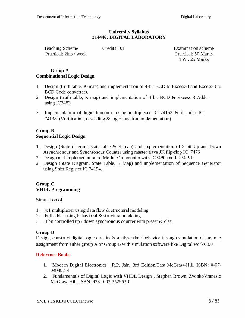
Department of Information Technology Digital Laboratory
SNJBrsquos LS KBJrsquos COEChandwad 4 85
3 Digital Logic applications and Design John Yarbrough Thomson PublicationISBN
978-0314066756
Instructor will frame assignments based on the suggested assignments as given above Students
will submit the term work in the form of journal consisting of 9 assignments listed above
Practical examination will be based on practical assignments and questions will be asked to
judge the understanding of assignments performed at the time of examination
Note - Instructor should take care that datasheets of all the required ICs are available in
the laboratory amp students are verifying the functionality of ICs being used
INDEX
Sr
No Title
Page No
Group A Combinational circuit design
1 Design amp implement 4 bit Code Converterhelliphelliphelliphelliphelliphelliphelliphelliphelliphelliphelliphelliphelliphellip 1
a BCD to Excess-3
b Excess-3 to BCD
2 Design amp implement BCD amp Excess 3 Adder using IC 7483helliphelliphellip 11
BCD amp Excess 3 Adder using IC 7483(4 bit binary adder)
3 Implementation of logic functions using multiplexer IC 74153 amp decoder IC
74138
18
(Verification cascading amp logic function implementation)
Group B Sequential Logic Design
4 Design amp implement 3 bit Asynchronous amp Synchronous counter 28
a 3 bit up Asynchronous counter
b 3 bit down Asynchronous counter
c 3 bit up Synchronous counter
d 3 bit down Synchronous counter
5 Design amp implement Modulus- N counterhelliphelliphelliphelliphelliphelliphelliphelliphelliphelliphelliphelliphelliphelliphellip 40
a Using IC 7490 (BCD counter)
b Using IC 74191 (Binary counter)
6 Design amp implement sequence generator using shift register IC 74194 54
Group C VHDL Programming amp simulation
7 Simulation of 41 mux helliphelliphelliphelliphelliphelliphelliphelliphelliphelliphelliphelliphelliphelliphelliphelliphelliphelliphelliphelliphelliphellip 61
a Using data flow modeling
b Using structural modeling
8 Simulation of Full Adderhelliphelliphelliphelliphelliphelliphelliphelliphelliphelliphelliphelliphelliphelliphelliphelliphelliphelliphelliphelliphellip 66
a Using behavioral modeling
b Using structural modeling
9 Simulation of 3 bit controlled updown Synchronous counter with preset amp clear 72
a Using data flow modeling
b Using behavioral modeling
Regularity Content Viva-voce Timely
Submission Total
Dated Sign of
Subject
Teacher
2 4 2 2 10
Date of Performance Date of Completion
-------------------------------------------------------------------------------------------------------------------
Assignment No 1
-------------------------------------------------------------------------------------------------------------------------------
Title Code Converter
------------------------------------------------------------------------------------------------------------------
Objective To learn and understand design and construction of combination circuit BCD to Excess-3
and Excess-3 to BCD code convertor
-------------------------------------------------------------------------------------------------------------------
Problem Statement Design (truth table K-map) and implementation of 4-bitBCD to Excess-3
and Excess-3 to BCD Code converters
-----------------------------------------------------------------------------------------------------------------
Hardware Requirement
i) IC 7404(Not-gate) 7432 (OR-gate) 7408 (AND-gate) 7486 (Ex-or gate)
ii) Digital Trainer Kit -1
iii) Patch cords
----------------------------------------------------------------------------------------------------------------
Software Requirement Digital Work 30
Theory
Introduction There is a wide variety of binary codes used in digital systems Some of these codes are
binary- coded -decimal (BCD) Excess-3 Gray octal hexadecimal etc Often it is required to convert
from one code to another For example the input to a digital system may be in natural BCD and output
may be 7-segment LEDs The digital system used may be capable of processing the data in straight binary
format Therefore the data has to be converted from one type of code to another type for different
purpose The various code converters can be designed using gates
Department of Information Technology Digital Laboratory
1
1 BCD Code
Binary Coded Decimal (BCD) is used to represent each of decimal digits (0 to 9) with a 4-bit binary code
For example (23)10 is represented by 0010 0011 using BCD code rather than(10111)2 This code is also
known as 8-4-2-1 code as 8421 indicates the binary weights of four bits(23 22 21 20) It is easy to convert
between BCD code numbers and the familiar decimal numbers It is the main advantage of this code With
four bits sixteen numbers (0000 to 1111) can be represented but in BCD code only 10 of these are used
The six code combinations (1010 to 1111) are not used and are invalid
Applications Some early computers processed BCD numbers Arithmetic operations can be performed
using this code Input to a digital system may be in natural BCD and output may be 7-segment LEDs
It is observed that more number of bits are required to code a decimal number using BCD code than using
the straight binary code However in spite of this disadvantage it is very convenient and useful code for
input and output operations in digital systems
Fig 1 BCD Coded Decimal Representation
2 EXCESS-3 Code
Excess-3 also called XS3 is a non-weighted code used to express decimal numbers It can be used for the
representation of multi-digit decimal numbers as can BCDThe code for each decimal number is obtained
by adding decimal 3 and then converting it to a 4-bit binary number For eg decimal 2 is coded as 0010 +
0011 = 0101 in Excess-3 code
This is self-complementing code which means 1rsquos complement of the coded number yields 9rsquos
complement of the number itself Self-complementing property of this helps considerably in performing
subtraction operation in digital systems so this code is used for certain arithmetic operations
Department of Information Technology Digital Laboratory
2
BCD To Excess ndash 3 Code Conversions
Convert BCD 2 i e 0010 to Excess ndash 3 code
For converting 4 bit BCD code to Excess ndash 3 add 0011 i e decimal 3 to the respective code using rules of
binary addition
0010 + 0011 = 0101 ndash Excess ndash 3 code for BCD 2
Excess ndash 3 Code To BCD Conversion
The 4 bit Excess-3 coded digit can be converted into BCD code by subtracting decimal value 3 ie 0011
from 4 bit Excess-3 digit
eg Convert 4-bit Excess-3 value 0101 to equivalent BCD code
0101-0011= 0010- BCD for 2
A BCD To Excess-3 Code Conversion
Step 1 Truth Table
INPUT (BCD CODE) OUTPUT (EXCESS-3 CODE)
B3 B2 B1 B0 E3 E2 E1 E0
0 0 0 0 0 0 1 1
0 0 0 1 0 1 0 0
0 0 1 0 0 1 0 1
0 0 1 1 0 1 1 0
0 1 0 0 0 1 1 1
0 1 0 1 1 0 0 0
0 1 1 0 1 0 0 1
0 1 1 1 1 0 1 0
1 0 0 0 1 0 1 1
1 0 0 1 1 1 0 0
Department of Information Technology Digital Laboratory
3
Step 2 K-Map For Reduced Boolean Expressions Of Each Output
Fig 2 K-Map for Reduced Boolean Expressions Of Each Output (Excess-3 Code)
Department of Information Technology Digital Laboratory
4
Step3 Circuit Diagram Test the circuit for all possible combinations of input and output codes
4) Hardware Requirements Table
Table 1 Hardware Requirement Table
GATE Quantity
IC Quantity
XOR 1 7486 1
NOT 4 7404 1
AND 4 7408 1
OR 3 7432 1
Department of Information Technology Digital Laboratory
5
B Excess-3 To BCD Conversion
1 Truth Table
INPUT (EXCESS-3 CODE) OUTPUT (BCD CODE)
E3 E2 E1 E0 B3 B2 B1 B0
0 0 0 0 X X X X
0 0 0 1 X X X X
0 0 1 0 X X X X
0 0 1 1 0 0 0 0
0 1 0 0 0 0 0 1
0 1 0 1 0 0 1 01O6
51
0 1 1 0 0 0 1 1
0 1 1 1 0 1 0 0
1 0 0 0 0 1 0 1
1 0 0 1 0 1 1 0
1 0 1 0 0 1 1 1
1 0 1 1 1 0 0 0
1 1 0 0 1 0 0 1
1 1 0 1 X X X X
1 1 1 0 X X X X
1 1 1 1 X X X X
Department of Information Technology Digital Laboratory
6
2) K-Map For Reduced Boolean Expressions Of Each Output
Fig 5 K-Map For Reduced Boolean Expressions Of Each Output (BCD Code)
Department of Information Technology Digital Laboratory
7
3) Circuit Diagram Test the circuit for all possible combinations of input and output codes
4) Hardware Requirements Table
Table 2 Hardware Requirement Table
GATE Quantity
IC Quantity
XOR 1 7486 1
NOT 3 7404 1
AND 8 7408 2
OR 3 7432 1
Pin Diagrams
Department of Information Technology Digital Laboratory
8
7400 Quad 2-Input NAND Gate
7402 Quad 2-Input NOR Gate
7404 Not Gates
7408 Quad 2-Input AND Gates
7432 Quad 2-Input OR Gate
7486 Quad 2-Input Exclusive-OR Gate
Department of Information Technology Digital Laboratory
9
Conclusion
Thus we studied different codes and their conversions including applications
The truth tables have been verified using IC 7486 7432 7408 and 7404
FAQrsquos with answers
Q1) What is the need of code converters
There is a wide variety of binary codes used in digital systems Often it is required to convert from one
code to another For example the input to a digital system may be in natural BCD and output may be 7-
segment LEDs The digital system used may be capable of processing the data in straight binary format
Therefore the data has to be converted from one type of code to another type for different purpose
Q2) What is Gray code
It is a modified binary code in which a decimal number is represented in binary form in such a way that
each Gray- Code number differs from the preceding and the succeeding number by a single bit
(eg for decimal number 5 the equivalent Gray code is 0111 and for 6 it is 0101 These two codes differ
by only one bit position i e third from the left) It is non weighted code
Q3) What is the significance of Gray code
Important feature of Gray code is it exhibits only a single bit change from one code word to the next in
sequence Whereas by using binary code there is a possibility of change of all bits if we move from one
number to other in sequence (eg binary code for 7 is 0111 and for 8 it is 1000) Therefore it is more
useful to use Gray code in some applications than binary code
Q4) What are applications of Gray code
1 Important feature of Gray code is it exhibits only a single bit change from one code word to the next in
sequence This property is important in many applications such as Shaft encoders where error
susceptibility increases with number of bit changes between adjacent numbers in sequence
2 It is sometimes convenient to use the Gray code to represent the digital data converted from the analog
data (Outputs of ADC)
3 Gray codes are used in angle-measuring devices in preference to straight forward binary encoding
Department of Information Technology Digital Laboratory
10
4 Gray codes are widely used in K-map
Q5) What are weighted codes and non-weighted codes
In weighted codes each digit position of number represents a specific weight The codes 8421 2421 and
5211 are weighted codes Non weighted codes are not assigned with any weight to each digit position ie
each digit position within the number is not assigned a fixed value Gray code Excess-3 code are non-
weighted code
Q6) Why is Excess-3 code called as self-complementing code
Excess-3 code is called self-complementing code because 9rsquos complement of a coded number can be
obtained by just complementing each bit
Q7) What is invalid BCD
With four bits sixteen numbers (0000 to 1111) can be represented but in BCD code only 10 of these are
used as decimal numbers have only 10 digits fro 0 to 9 The six code combinations (1010 to 1111) are not
used and are invalid
Department of Information Technology Digital Laboratory
11
Regularity Content Viva-voce Timely
Submission Total
Dated Sign of
Subject
Teacher
2 4 2 2 10
Date of Performance Date of Completion
-------------------------------------------------------------------------------------------------------------------
Assignment No 2
------------------------------------------------------------------------------------------------------------------
Title BCD amp Excess 3 Adder
------------------------------------------------------------------------------------------------------------------
Objective 1 To study the BCD arithmetic rules
2 Comparison between binary and BCD codes
Problem Statement Design (truth table K-map) and implementation of 4-bit BCD to Excess-3 and
Excess-3 to BCD Code converters
-----------------------------------------------------------------------------------------------------------------
Hardware Requirement
i) IC 7483 (4 bit Binary adder) IC 7404(Hex INV) 7432 (OR-gate) 7408 (AND-gate)
ii) 7486 (EX-OR gate)
iii) Digital Trainer Kit -1
iv) Patch cords
----------------------------------------------------------------------------------------------------------------
Software Requirement Digital Work 30
------------------------------------------------------------------------------------------------------------------
Theory
BCD-Binary coded decimal-In this code each decimal digit represent by a 4-bit binary no BCD is a
way to express each of the decimal digits with binary code Positional weights associated to the binary bits
in BCD code are (MSB) 8-4-2-1(LSB)
BCD number 0 to 9 but greater than 9 is invalid BCD
Department of Information Technology Digital Laboratory
12
So Convert in valid BCD using add 6 ie (0110)
BCD Adder
BCD adder is a circuit that adds two BCD digits amp produces a sum of digits also in BCD
Rules for BCD addition
1 Add two numbers using rules of Binary addition
2 If the 4 bit sum is greater than 9 or if carry is generated then the sum is invalid To correct the sum
add 0110 i e (6)10 to sum If carry is generated from this addition add it to next higher order BCD
digit
3 If the 4 bit sum is less than 9 or equal to 9 then sum is in proper form
CASE I Sum lt= 9 amp carry = 0
Add BCD digits 3 amp 4
1 0 0 1 1
+ 0 1 0 0
------------
0 1 1 1
Answer is valid BCD number = (7)BCDamp so 0110 is not added
CASE II Sum gt 9 amp carry = 0
Add BCD digits 6 amp 5
1 0 1 1 0
+ 0 1 0 1
-----------
10 1 1
Department of Information Technology Digital Laboratory
13
Invalid BCD (since sum gt 9) so 0110 is to be added
2 1 0 1 1
+ 0 1 1 0
-----------
1 0 0 0 1
(1 1)BCD
Valid BCD result = (11) BCD
CASE III Sum lt = 9 amp carry = 1
Add BCD digits 9 amp 9
1 1 0 0 1
+1 0 0 1
-----------
1 0 0 1 0
Invalid BCD ( since Carry = 1 ) so 0110 is to be added
2 1 0 0 1 0
+ 0 1 1 0
------------
1 1 0 0 0
(1 8)BCD
Valid BCD result = (18) BCD
Design of BCD adder
1 To execute first step i e binary addition of two 4 bit numbers we will use IC 7483
( withCin = 0 ) which is 4 bit binary adder
2 We need to design a digital circuit which will sense sum amp carry of IC 7483 amp if sum exceeds 9 or
carry = 1 this digital circuit will produce high output otherwise its output will be zero
Circuit to check invalid BCD
Department of Information Technology Digital Laboratory
14
First we will design circuit to check sum amp then we will logically OR output of this circuit to carry
output of IC 7483
For digital circuit which we are going to design we will have 4 inputs
( S3 S2 S1 S0) amp only 1 output Y
a) Y output of this circuit Will be ORed with carry output of first adder IC
7483
b) If BCD result is invalid i e sum output of first 7483 we have to add
(6)10 ie (0110)2 that means we need one more binary adder IC 7483
c) If BCD result is valid ( ie final output of the circuit to check validity is 0) we will make an
arrangement that second adder IC 7483 adds (0)10 i e ( 0000 )2 to the sum of the first adder IC 7483
The output of the combinational circuit is used as final output carry amp carry output of second adder IC is
ignored
i ) Truth Table for design of combinational circuit for BCD adder to check invalid
BCD
K-map for output- Y=S3S2+S3S1
Department of Information Technology Digital Laboratory
15
iii) Circuit diagram
v) Hardware Requirements
GATE Quantity
IC Quantity
Binary adder 2 7483 2
AND 2 7408 1
OR 2 7432 1
B ) Design and Implement single digit EXCESS-3 adder using IC 7483
Excess-3 code is a non weighted code It is a modified form of a BCD code The Excess-3 code can be
derived from the natural BCD code by adding 3 to each coded number It is also known as Self
Complementary code
Excess-3 code is a self complementary code because 1rsquos complement of Excess-3 number is Excess-3
code for the 9rsquos complement of corresponding number
Output of BCD adder
Department of Information Technology Digital Laboratory
16
Eg Excess-3 code for (4)10 is (0111)XS-3 1rsquos complement of this number is 1000 which is Excess-3 code
for (5)10and 5 is 9rsquos complement of (4)10
Rules for Excess-3 addition
i Add two Exceess-3 numbers
ii If carry is 1 add 3 to Sum
iii If carry is 0 subtract 3 from sum
Eg (8)10 + (6)10
(8)10 = 1011 (Excess-3 for 8)
(6)10= 1001 (Excess-3 for 6)
_______________
1 0100
0011 0011
_______________
0100 0111 ( Excess 3 code for (14)10
(i)Design
1) 4 bit Binary addition of excess 3 codes of two operands can be implemented with IC 7483
2) We have to design the circuit which will either add 0011 or subtract 0011 ie add 1101 (2rsquos
complement of 0011)depending upon carry bit
Letrsquos compare 0011 and 1101
B3 B2 B1 B0
0 0 1 1 ------- When carry is 1
1 1 0 1 ------- When carry is 0
Here B0 bit in both situation is High
Now compare B3 B2 and B1 It is complement of each other
When carry is 1 Bit B1 =1 B2=B3=0
When carry is 0 Bit B1 =0 B2=B3=1
B1 bit follows the carry and B2 and B3 bit complements the carry
(ii) Circuit Diagram
Department of Information Technology Digital Laboratory
17
(iii ) HARDWARE REQUIREMENTS
Sl No IC Description Quantity
1 7404 Not Gate 01
2 7483 4 bit Binary Adder 04
CONCLUSION
BCD adder ampsubtractor is designed amp tested for all possible combinations
FAQrsquos
1 Explain and Write the significance of BCD number system
2 Write the applications of BCD amp Excess 3 code
3 Explain the rules of BCD amp Excess 3 arithmetic
4 What is the difference between BCD and binary codes
5 What do you mean by unpacked and packed BCD nos
Department of Information Technology Digital Laboratory
18
Regularity Content Viva-voce Timely
Submission Total
Dated Sign of
Subject
Teacher
2 4 2 2 10
+
Date of Performance Date of Completion
-------------------------------------------------------------------------------------------------------------------
Assignment No 3
---------------------------------------------------------------------------------------------------------------------------
Title Implementation of logic functions
----------------------------------------------------------------------------------------------------------------------
Objective 1 To study the difference between multiplexer demultiplexer and decoder
2To study the applications of multiplexer
---------------------------------------------------------------------------------------------------------------------
Problem Statement Implement of Logic function using multiplexer IC 74153
---------------------------------------------------------------------------------------------------------------------
Hardware Requirement
i) IC 74153 74138 7404 7432
ii) Digital Trainer Kit -1
iii) Patch cords
----------------------------------------------------------------------------------------------------------------
Software Requirement Digital Work 30
------------------------------------------------------------------------------------------------------------------
Theory
D CWigital Multiplexer
Multiplexer are combinational digital circuits equating as controlled switches with several data inputs (I0
I1 I2 hellip) amp one single data output (ldquooutrdquo)At any time one of the Ip is transmitted to output According to
binary signals applied on control pairs to circuit Usually the number of data inputs is a power of two
Multiplexing is the process of transmitting a large no of information units over a small no of channel
digital multiplexer is a combinational large circuit which performs the operation of multiplexing It selects
Department of Information Technology Digital Laboratory
19
the operation of multiplexing It selects the operation of binary information from one of the many input
lines amp transfer to a single op line Multiplexer is called a data selector or multiposition switch because it
selects one of the many input Selection of a particular line is controlled by a set of a selection lines or
selects inputs The number of select lines depends upon no of input lines Generally there
is lsquonrsquo selects line for lsquomrsquo input lines By applying a particular code on select lines is transmitted on the
output linesBlock diagram of MUX is shown at contains lsquo2mrsquo input lines lsquomrsquo select Such that 2m = n amp
one unable input which is used to activate or dedicate MUX Depending upon the no of IP amp OP lines
various types of multiplexers are available We have 21 41 81 161 MUX Here the first no indicates
the no of input lines amp second no indicates the no of output lines
E is called as enable input which is generally active low
Fig-Block diagram for N1 Multiplxer
Demultiplexer
Demultiplexer is a logic used to perform exactly reverse function performed by multiplexer It accepts a
single input and distributes among several outputs The selection of a particular output line is controlled
by a set of selection line There are n input lines amp 2m is the number of selection line whose bit
combinations determine which output to be selected
Encoder amp Decoder
1 Encoders are used to encode given digital number into different numbering format like
decimal to BCD Encoder Octal to Binary
2 Decoders are used to decode a coded binary word like BCD to seven segment decoder
3 Thus encoder and decoder are application specific logic develop we can not use any type of
input for any encoder and decoder
Smhelliphellips1 s0
Output(Y)
D0
D1
D2
D3
Dn
N1
multiplxer
E
Department of Information Technology Digital Laboratory
20
4 Need to select input according to encoder and decoder being selected for a particular
application as mention in examples above
Uses of Mux
1 Use for Boolean function implementation
2 Construct a common bus system
3 To select between multiple sources amp signal destination
4 Inter register transfer
Advantages
1) Simplification of logic expression not required
2) Logic design is simplified
Disadvantage
Only one function can be implemented using one MUX Hence they canrsquot be used in
combinational logic circuit which contains many function
Part-A (IC 74153)
1 VERIFICATION OF IC 74153
IC 74153 is a dual layer 41 MUX It has four input lines for (I0D-I3D) for second MUX amp active high
output lsquoYarsquo lsquoYbrsquo (1Y or 2Y) It has select lines S1S0 common to both MUX The Enable inputs are
active low EaampEb(1G and 2G) The MUX is activated when they are at logic o
Pin out of IC 74153
Department of Information Technology Digital Laboratory
21
Function table of IC 74153 (X= Donrsquot Care Condition)
Select Input
Inputs (I or II) Output
S1 S0 E (I or II) D0 D1 D2 D3 Y
X X 1 X X X X 0
0 0 0 0 X X X 0
0 0 0 1 X X X 1
0 1 0 X 0 X X 0
0 1 0 X 1 X X 1
1 0 0 X X 0 X 0
1 0 0 X X 1 X 1
1 1 0 X X X 0 0
1 1 0 X X X 1 1
2CASCADING OF IC 74153
Cascading is done to expand two or more MUX ICrsquos to a digital multiplexer with larger no of inputs ie
multiplexer stocks or tress is designed The enable input is used for cascading In case of IC 74153 we
have only two select lines But for certain application 3 select lines are required then it can be
obtained by cascading using enable Now with 3 select lines we have 8 combinations Out of this
combination the MSB is O MSB is 1 for last four combination so we can use these MSB to select
any 1 MUX out of two by connecting it to E pin of first 41 MUX
Function table of IC 74153 as 8 1 Mux by cascading 2 41 Mux
Select Input Output
C (1G 2G ) B (S1) A (S0) Y
0 0 0 D0
0 0 1 D1
0 1 0 D2
0 1 1 D3
1 0 0 D4
1 0 1 D5
Department of Information Technology Digital Laboratory
22
1 1 0 D6
1 1 1 D7
3FUNCTION IMPLEMENTATION
Y= sum m (1 3 5 6)
Thisexpression is in Standard SOP form and it is three variable function So we need to use mux with
three select inputs ie 81 Mux Already we have implemented 81 Mux using IC 74153 For Boolean
function in Standard SOP form we connect data inputs corresponding to the minterms present in the given
function to Vcc and remaining data inputs to ground
Truth table
Inputs Output
C B A Y
0 0 0 0
0 0 1 1
0 1 0 0
0 1 1 1
1 0 0 0
1 0 1 1
1 1 0 1
1 1 1 0
LOGIC DIAGRAM
Hardware Requirements
GATE Quantity
IC Quantity
Mux 1 74153 1
NOT 1 7404 1
OR 1 7432 1
Department of Information Technology Digital Laboratory
23
Part-B Decoder (IC 74138)
Theory
Discrete quantities of information are requested in digital system with binary codes A binary code of n
bits is capable of representing into 2n distinct elements of the coded information
Decoder converts coded input to coded outputs accepts one of the code
There are different types of decoders such as 38 decoder 416 line decoders etc These are in general
called as n m line decoder where m=2n and n= no of input lines and m=no of output lines Demux also
takes one input data line source and selectively distributes it to one of n output channels The only
difference between demux and decoder is that demux has Din (data ip) line whereas decoder does not
have
ADVANTAGES
1) The decoder provides best implementation whenever there are many outputs of the combinational
circuit and each op of the function (or its complement) is required to be expressed with a small no
of minterms
2) The decoder can function as demux If the Enable ip line is taken as Din (data ip)
DISADVANTAGES
Since decoder method requires an OR gate for each op function so there is new hardware used And it is
always advisable to use minimum hardware as we come across problems like propagation delay of gates
APPLICATIONS
Decoder is worthily used for decoding binary information and memory interfacing It is used for the
implementation of Boolean function
Differentiate between Mux Demux Decoder
Point Multiplexer Demultiplexer Decoder
Input Many input lines Single input line Many input line also Acts as select line
Output Single output line Many output line Many output lineActive low output
Select line 2m = n n = 2m Enable inputs used
Department of Information Technology Digital Laboratory
24
A) Verification of IC 74138
We use IC 74138 which accepts 3 binary weighted inputs (A0 A1 A2) and when enabled provides
mutually exclusive active low outputs (y0-y7) It features 3 Enable ips Two active low (G2A G2B) and
one active high (G1) Every output will be high unless G2A G2Bare low and G1 is high It has
demultiplexing capability and multiple enable ips for easy expansion
IC Diagram
Function Table of 38 decoder
Input Output
Enable Data
G2A G2B G1 A2 A1 A0 Y0 Y1 Y2 Y3 Y4 Y5 Y6 Y7
0 0 0 X X X 1 1 1 1 1 1 1 1
0 1 1 X X X 1 1 1 1 1 1 1 1
1 0 1 X X X 1 1 1 1 1 1 1 1
1 1 1 X X X 1 1 1 1 1 1 1 1
Department of Information Technology Digital Laboratory
25
0 0 1 0 0 0 0 1 1 1 1 1 1 1
0 0 1 0 0 1 1 0 1 1 1 1 1 1
0 0 1 0 1 0 1 1 0 1 1 1 1 1
0 0 1 0 1 1 1 1 1 0 1 1 1 1
0 0 1 1 0 0 1 1 1 1 0 1 1 1
0 0 1 1 0 1 1 1 1 1 1 0 1 1
0 0 1 1 1 0 1 1 1 1 1 1 0 1
0 0 1 1 1 1 1 1 1 1 1 1 1 0
B) Cascading of IC 74138
The enable ip G1 active high of IC 74138 is used for cascadingfor cascading 2 ICrsquos the enable ip G1 of
first IC is connected to G1 enable ip of second IC through a NOT gate This enable ip is used as MSB
select ip line A3 the other three select input lines of both ICrsquos (A0A1A2) are also shorted to select
input lines of second IC to get single ip select lines (A0A1A2)
The ip line A3 is used to enable disable the 2 IC 74138 decoders When A3=0 first IC is enabled and
second is disabled Thus the first decoder will generate minterms from 0000 to 0111 as op and the second
decoder will generate nothing When A3=1 the enable conditions are reversed and thus second decoder
IC will generate minterms 1000 to 1111
Function Table of 416 decoder using IC 74138 (38 decoder)
Input Output
Enable Data
G2
A
G2
B
A
3
A
2
A
1
A
0
Y
0
Y
1
Y
2
Y
3
Y
4
Y
5
Y
6
Y
7
Y
8
Y
9
Y1
0
Y1
1
Y1
2
Y1
3
Y1
4
Y1
5
0 1 X X X X 1 1 1 1 1 1 1 1 1 1 1 1 1 1 1 1
Department of Information Technology Digital Laboratory
26
1 0 X X X X 1 1 1 1 1 1 1 1 1 1 1 1 1 1 1 1
1 1 X X X X 1 1 1 1 1 1 1 1 1 1 1 1 1 1 1 1
0 0 0 0 0 0 0 1 1 1 1 1 1 1 1 1 1 1 1 1 1 1
0 0 0 0 0 1 1 0 1 1 1 1 1 1 1 1 1 1 1 1 1 1
0 0 0 0 1 0 1 1 0 1 1 1 1 1 1 1 1 1 1 1 1 1
0 0 0 0 1 1 1 1 1 0 1 1 1 1 1 1 1 1 1 1 1 1
0 0 0 1 0 0 1 1 1 1 0 1 1 1 1 1 1 1 1 1 1 1
0 0 0 1 0 1 1 1 1 1 1 0 1 1 1 1 1 1 1 1 1 1
0 0 0 1 1 0 1 1 1 1 1 1 0 1 1 1 1 1 1 1 1 1
0 0 0 1 1 1 1 1 1 1 1 1 1 0 1 1 1 1 1 1 1 1
0 0 1 0 0 0 1 1 1 1 1 1 1 1 0 1 1 1 1 1 1 1
0 0 1 0 0 1 1 1 1 1 1 1 1 1 1 0 1 1 1 1 1 1
0 0 1 0 1 0 1 1 1 1 1 1 1 1 1 1 0 1 1 1 1 1
0 0 1 0 1 1 1 1 1 1 1 1 1 1 1 1 1 0 1 1 1 1
0 0 1 1 0 0 1 1 1 1 1 1 1 1 1 1 1 1 0 1 1 1
0 0 1 1 0 1 1 1 1 1 1 1 1 1 1 1 1 1 1 0 1 1
0 0 1 1 1 0 1 1 1 1 1 1 1 1 1 1 1 1 1 1 0 1
0 0 1 1 1 1 1 1 1 1 1 1 1 1 1 1 1 1 1 1 1 0
C) Implementation of Boolean function
The procedure for implementation of combinational circuit by means of a decoder and lsquoORrsquo gates requires
that the Boolean function fir the circuit be expressed in Sum of Minterms These forms can be obtained by
Department of Information Technology Digital Laboratory
27
expanding the function A decoder is then chosen which generates all the minterms of n ip variables The
ip to each OR gate are selected from the decoder outputs according to the minterms list in each function
i) F1=summ (1 3 5 7)
Truth table
Logic Diagram
ii) F2=summ (1 3 5 7111315)
Truth table
Logic Diagram
Conclusion In this way multiplexer Decoderamp its applications are studied implemented amp
tested
FAQrsquos
1What is a multiplexer
2What is a Demultiplexer
3 Enlist applications of multiplexer
Department of Information Technology Digital Laboratory
28
Regularity Content Viva-voce Timely
Submission Total
Dated Sign of
Subject
Teacher
2 4 2 2 10
Date of Performance Date of Completion
-------------------------------------------------------------------------------------------------------------------
Assignment No4
------------------------------------------------------------------------------------------------------------------
Title 3 bit updown Asynchronous and Synchronous counter using IC7476
------------------------------------------------------------------------------------------------------------------
Objective To understand design procedure of asynchronousamp Synchronous counter
------------------------------------------------------------------------------------------------------------------
Problem Statement Design (State diagram state table amp K map) and implementation of 3
bit Up and Down Asynchronous and Synchronous Counter using master slave JK flip-flop IC 7476
-----------------------------------------------------------------------------------------------------------------
Hardware Requirement
i) IC 7476 (MS-JK Flip-flop) IC 7408(Quad 2 ip AND Gate)
IC 7432 (Quad 2 ip OR Gate) and IC 7404 (Hex Inverter)
ii) Digital Trainer Kit -132
iii) Patch cords
----------------------------------------------------------------------------------------------------------------
Software Requirement Digital Work 30
------------------------------------------------------------------------------------------------------------------
Theory
Counters counters are logical device or registers capable of counting the no of states or no of clock
pulses arriving at its clock input where clock is a timing parameter arriving at regular intervals of time
so counters can be also used to measure time amp frequencies They are made up of flip flops Where the
Department of Information Technology Digital Laboratory
29
pulse are counted to be made of it goes up step by step amp the op of counter in the flip flop is decoded to
read the count to its starting step after counting n pulse incase of module counters
Types of Counters
Counter are of two types
1) Asynchronous counter
2) Synchronous counter
Asynchronous counter
A digital counter is a set of flip flop The flip flop are connected such that their combined state at any time
is binary equivalent of total no of pulses that have occurred up to that time Thus its name implies a
counter is used to count pulse A counter is used as frequency dividers To obtain waveform with
frequency that is specific fraction of clock frequency
Counter may be Asynchronous or synchronous The Asynchronous counter is also called as ripple counter
An Asynchronous counter uses T flip flop to perform a counting function The actual hardware used is
usually J-K flip flop with J amp K connected to logic1Even D flip flops may be used here
In asynchronous counter commonly called ripple counter the first flip-flop is clocked by the external
clock pulse amp then each successive flip-flop is clocked by the Q or Qrsquo output of the previous flip-flop
Therefore in an asynchronous counter the flip-floprsquos are not clocked simultaneously The input of MS-JK
is connected to VCC because when both inputs are one output is toggled As MS-JK is negative edge
triggered at each high to low transition the next flip-flop is triggered
Synchronous Counter
When counter is clocked such that each flip flop in the counter is
triggered at the same time the counter is called as synchronous counter
The gates propagation delay at reset time will not be present or we may say will not occur
1) Asynchronous Up Counter
Fig 1 shows 3bit Asynchronous Up Counter Here Flip-flop 2 act as a MSB Flip-flop and Flip-flop 0 act
as a LSB Flip-flop Clock pulse is connected to the Clock of Flip-flop 0 Output of Flip-flop 0(Q0) is
connected to clock of next flip-flop (ie Flip-flop 1) and so on As soon as clock pulse changes output is
going to change (at the negative edge of clock pulse) as a Up count sequence For 3 bit Up counter state
table is as shown below
Department of Information Technology Digital Laboratory
30
State Table
Logic diagram
Fig 1 3 Bit Asynchronous Up Counter
Hardware requirements
Gate
Flip flop
Quantity IC Quantity
MS JK 3 7476 2
2) Down Counter
Fig 2 shows 2 bit Asynchronous Down Counter Here Flip-flop 2 act as a MSB Flip-flop and Flip-flop 0
act as a LSB Flip-flop Clock pulse is connected to the Clock of Flip-flop 0 Output of Flip-flop 0 (Q0rsquo) is
Counter States Count
Q2 Q1 Q0
0 0 0 0
1 0 0 1
2 0 1 0
3 0 1 1
4 1 0 0
5 1 0 1
6 1 1 0
7 1 1 1
8 0 0 0
Department of Information Technology Digital Laboratory
31
connected to clock of next flip-flop (ie Flip-flop 1) and so on As soon as clock pulse changes output is
going to change (at the negative edge of clock pulse) as a down count sequence For 3 bit down counter
sate table is as shown below
In both the counters Inputs J and K are connected to Vcc hence J-K Flip flop work in toggle mode Preset
and Clear both are connected to logic 1
State Table
Logic diagram
Fig 2 3 Bit Asynchronous Down Counter
Hardware requirements
Counter States Count
Q2 Q1 Q0
7 1 1 1
6 1 1 0
5 1 0 1
4 1 0 0
3 0 1 1
2 0 1 0
1 0 0 1
0 0 0 0
7 1 1 1
Department of Information Technology Digital Laboratory
32
Gate
Flip flop
Quantity IC Quantity
MS JK 3 7476 2
Applications
The asynchronous counters are specially used as the counting devices
They are also used to count number of pulses applied
It also works as frequency divider
It helps in counting the number of product coming out of the machinery where product is coming out at
equal interval of time
Types of synchronous counter
1) Up counter
2) Down counter
1 3 bit Synchronous up counter
The up counter counts from 0 to7 ie(000 to 111)for this we are using MS JK flip flop In IC 74LS76 2
MS J-K flip flops are present The clock pulse is given at pin 1 amp 6 of the 1st IC amp pin 1 of 2nd IC Next
state decoder logic is designed with the help of state table
State table for synchronous up counter
Present state Next state Flip flop 3 Flip flop 2 flip flop 1
Q2 Q1 Q0 Q2 Q2 Q0 J2 K2 J1 K1 J0 K0
0 0 0 0 0 1 0 x 0 X 1 x
0 0 1 0 1 0 0 x 1 X x 1
0 1 0 0 1 1 0 x x 0 1 x
0 1 1 1 0 0 1 x x 1 x 1
1 0 0 1 0 1 x 0 0 X 1 X
1 0 1 1 1 0 x 0 1 X x 1
1 1 0 1 1 1 x 0 x 0 1 X
1 1 1 0 0 0 x 1 x 1 x 1
Department of Information Technology Digital Laboratory
33
K-Map
Q1Q0
Q2
00 01 11 10
0 0 0 1 0
1 X X X X
J2= Q1Q0
Q1Q0
Q2
00 01 11 10
0 X X X X
1 0 0 1 0
K2= Q1Q0
Q1Q0
Q2
00 01 11 10
0 0 1 X X
1 0 1 X X
J1= Q0
Q1Q0
Q2
00 01 11 10
0 X X 1 0
1 X X 1 0
K1= Q0
Department of Information Technology Digital Laboratory
34
Q1Q0
Q2
00 01 11 10
0 1 X X 1
1 1 X X 1
J0= 1
Q1Q0
Q2
00 01 11 10
0 X 1 1 X
1 X 1 1 X
K0= 1
Logic Diagram
Fig 1 3 bit Synchronous up counter
Department of Information Technology Digital Laboratory
35
2 3 bit Synchronous down counter
This is used to count from 7-0 ie(111-000)for this also 2 ICrsquos of 74LS76 are required amp hence we use 3
MS JK flip flops Here also clock is given to 1stamp 6th pin of 1st IC amp1st pin of 2nd IC enabling to apply
clock to all flip flop at a time Next state decoder logic is designed with the help of state table
State table for synchronous down counter
Present state Next state Flip flop 3 Flip flop 2 Flip flop 1
Q2 Q1 Q0 Q2 Q1 Q0 J2 K2 J1 K1 J0 K0
1 1 1 1 1 0 X 0 X 0 X 1
1 1 0 1 0 1 X 0 X 1 1 X
1 0 1 1 0 0 X 0 0 X X 1
1 0 0 0 1 1 X 1 1 X 1 X
0 1 1 0 1 0 0 X X 0 X 1
0 1 0 0 0 1 0 X X 1 1 X
0 0 1 0 0 0 0 X 0 X X 1
0 0 0 1 1 1 1 X 1 X 1 X
K-Map
Q1Q0
Q2
00 01 11 10
0 1 0 0 0
1 X X X X
J2= Q1Q0
Q1Q0
Q2
00 01 11 10
Department of Information Technology Digital Laboratory
36
0 X X X X
1 1 0 0 0
K2= Q1Q0
Q1Q0
Q2
00 01 11 10
0 1 0 X X
1 1 0 X X
J1= Q0
Q1Q0
Q2
00 01 11 10
0 X X 0 1
1 X X 0 1
K1= Q0
Q1Q0
Q2
00 01 11 10
0 1 X X 1
1 1 X X 1
J0= 1
Q1Q0
Q2
00 01 11 10
0 X 1 1 X
1 X 1 1 X
K0= 1
Department of Information Technology Digital Laboratory
37
Logic Diagram
Fig 2 3 bit Synchronous down counter
Uses
1 Specially used as the counting devices
2 Used in frequency divider circuit
3 Used in digital voltmeter
4 Used in counter type A to D converter
5 Used for time measurement
6 It helps in counting the no of product coming out from machinery where product is coming out
at equal interval of time
Conclusion
Up and down counters are successfully implemented the counters are studied amp op are checked The
state table is verified
PRACTICE ASSIGNMENTS EXERCISE MODIFICATIONS
1 Design amp implement 2 bit controlled synchronous counter
2 Designamp implement 4 bit controlled synchronous counter
3 Designamp implement truncated synchronous up or down counter
FAQrsquos with answers
1 What do you mean by Counter
A Counter is a register capable of counting the no of clock pulses arriving at its
clock inputs Count represents the no of clock pulses arrived A specified
sequence of states appears as the counter output
Department of Information Technology Digital Laboratory
38
2 What are the types of Counters Explain each
There are two types of counters as Asynchronous Counter and Synchronous Counter
Asynchronous Counter In this counter the first flip-flop is clocked by the external clock pulse
and then each successive flip-flop is clocked by the Q or Qrsquo op of the previous flip-flop Hence in
Asynchronous Counter flip-flops are not clocked simultaneously and hence called as Ripple
Counter Synchronous Counter In this counter the common clock input is connected to all the
flip-flops simultaneously
3 What do you mean by pre-settable counters
A counter in which starting state is not zero can be designed by making use of the
preset inputs of the flip flops This is referred to as loading the counter
asynchronously This is referred to as pre-settable counter
4 What are the applications of synchronous counters
Digital clock
Frequency divider circuits
Frequency counters
Used in analog to digital converters
5 What are the advantages of synchronous counters over asynchronous counters
Propagation delay time is reduced
Can operate at a much higher frequency than the asynchronous counters
6 Ring counter is an example of synchronous counters or asynchronous counter
Synchronous counter Since all the flip flops are clocked simultaneously
7 Twisted Ring (Johnsonrsquos) counter is an example of synchronous counters or asynchronous
counter
Synchronous counter Since all the flip flops are clocked simultaneously
8 What is the difference between ring counter and twisted ring counter
In ring counter pulses to be counted are applied to a counter it goes from state to state and the
output of the flip flop s in the counter is decoded to read the count Here the uncomplimentary
output (Q) of last flip flop is fed back as an input to first flip flop Ring counters are referred as
MOD lsquoNrsquo counters
Department of Information Technology Digital Laboratory
39
But in Twisted ring counter the complimentary output (Q bar) of last flip flop is fed back as an
input to first flip flop Twisted Ring counters are referred as MOD lsquo2Nrsquo counters
9 What are the applications of ring counters
Ring counter outputs are sequential non-overlapping pulses which are useful for control state
counters Used in stepper motor this requires pulses to rotate it from one position to the next Used
as divide by lsquoNrsquo ((MOD lsquoNrsquo) counters
10 What are the applications of ring counter twisted ring counters
Used as divide by lsquo2Nrsquo ((MOD lsquo2Nrsquo) counters
Used for control state counters
Used for generation of multiphase clock
11 List the Synchronous Counter ICs
IC 74160 Decade Up Counter
IC 74161 4 bit binary Up Counter
IC 74162 Decade Up Counter
IC 74163 4 bit binary Up Counter
IC 74168 Decade UpDown Counter
IC 74169 4 bit Binary UpDown Counter
IC 74190 Decade UpDown Counter
IC 74191 4 bit Binary UpDown Counter
IC 74192 Decade UpDown Counter
IC 74193 4 bit Binary UpDown Counter
Department of Information Technology Digital Laboratory
40
Regularity Content Viva-voce Timely
Submission Total
Dated Sign of
Subject
Teacher
2 4 2 2 10
Date of Performance Date of Completion
-------------------------------------------------------------------------------------------------------------------
Assignment No 5
-------------------------------------------------------------------------------------------------------------------------------
Title Design and implementation of Module lsquonrsquo counter with IC7490 and IC 74191
-----------------------------------------------------------------------------------------------------------------------------
Objective To know difference between regular amp truncated counter as well as binary ampBCD Counter
--------------------------------------------------------------------------------------------------------------------------------
Problem Statement To design and implement mod - 10 mod ndash 7 mod - 99 asynchronous BCD
counter using IC 7490 and to design and implement up down mod - n Binary counter using IC 74191
-----------------------------------------------------------------------------------------------------------------
Hardware Requirement
i) IC 7490 IC 74191 basic gates
ii) Digital Trainer Kit -1
iii) Patch cords
----------------------------------------------------------------------------------------------------------------
Software Requirement Digital Work 30
------------------------------------------------------------------------------------------------------------------
Theory
Part A ndash IC 7490
IC 7490 is a TTL MSI (medium scale integration) decade counter It contains 4 master slave flip flops
internally connected to provide MOD-2 ie divide by 2 and MOD-5 ie divide by 5 counters MOD-2 and
Mod-5 counters can be used independently or in cascading
Department of Information Technology Digital Laboratory
41
It is a 4-bit ripple type decade counter The device consists of 4-master slave flip flops internally
connected to provide a divide by two and divide by 5 sections Each section has a separate clock ip to
initiate state changes of the counter on the high to low clock transition
Since the op from the divide by 2 section is not internally connected to the succeeding stages The device
may be operated in various counting modes In a BCD counter the CP1 input must be externally connected
to QA op The CP0ip receives the incoming count producing a BCD count sequence It is also provided
with additional gating to provide a divide by 2 counter and binary counter for which the count cycle length
is divide by 5 The device may be operated in various counting modes
There are 2 reset inputs R0(1) and R0(2) both of which need to be connected to the lsquologic 1rsquo for clearing all
flip flops Two set inputs Rg(1) and Rg(2) when connected to logic 1 are used for setting counter to 1001
(BCD 9)
Pin out of IC 7490
Fig Pin configuration of IC7490
Table 1-pin name and description of IC7490
Pin name Description
Input B This is clock input to the internal MOD-5 ripple counter which is negative
edge triggered
R0(1)R0(2) Gated zero reset inputs
Department of Information Technology Digital Laboratory
42
R9(1)R9(2) These are gated set to nine inputs
QDQCQB Output of internal MOD-5 counter with QD as MSB
QA Output of internal MOD-2 counter with QA as LSB
Input A Clock input to FF-A which is negative edge triggered
Functional Table for IC7490
Reset inputs Output
R0(1) R0(2) R9(0) R9(1) QD QC QB QA
1 1 0 X 0 0 0 0
1 1 X 0 0 0 0 0
X X 1 1 1 0 0 1
X 0 X 0 COUNTER
0 X 0 X COUNTER
0 X X 0 COUNTER
X 0 0 x COUNTER
Department of Information Technology Digital Laboratory
43
Basic internal Structure of IC 7490
Function Table of MOD-5 counter
Design of MOD-10 counter using IC 7490
The QA op the first flip flop is connected to the input B which is clock ip of internal MOD-5 ripple
counter Due to cascading of Mod-2 and Mod-5 counters the overall configuration the decade counters
count from 0000 to 1001 After 1001 mod-5 resets to 0000 and next count after 1001 is 0000
When QA op is connected to B ip we have the Mod-2 counter followed by Mod-5 counter The
count sequence obtained is shown in the table It may be noted that QA changes from 0 to 1 the state of
InputB clock Output
Count QD QC QB
0 0 0 0
0 0 1 1
0 1 0 2
0 1 1 3
1 0 0 4
Department of Information Technology Digital Laboratory
44
Mod-5 counter doesnrsquot change whereas when QA changes from 1 to 0 the Mod-5 counter goes to the next
state
Logic DiagramMOD-10 counter using IC 7490
5 Modulus n Counter
Function table
Ip clock
Output
Count QD QC QB QA
0 0 0 0 0
0 0 0 1 1
0 0 1 0 2
0 0 1 1 3
0 1 0 0 4
Department of Information Technology Digital Laboratory
45
Design of Mod-7 Counter using IC 7490
Mod-7 counter counts through seven states from 0 to 6 counters and it should reset as soon as the
count becomes 7 The op of reset logic should be 1 corresponding to invalid states The reset logic op
should be applied to pin 2 and 3
Truth Table of Reset Logic
0 1 0 1 5
0 1 1 0 6
0 1 1 1 7
1 0 0 0 8
1 0 0 1 9
QD QC QB QA Y
0 0 0 0 0
0 0 0 1 0
0 0 1 0 0
0 0 1 1 0
0 1 0 0 0
0 1 0 1 0
0 1 1 0 0
0 1 1 1 1
1 0 0 0 1
1 0 0 1 1
Department of Information Technology Digital Laboratory
46
Logic Diagram Mod 7 Counter using IC 7490
Function table
Ip clock
Output
Count QD QC QB QA
0 0 0 0 0
0 0 0 1 1
0 0 1 0 2
0 0 1 1 3
0 1 0 0 4
0 1 0 1 5
0 1 1 0 6
Department of Information Technology Digital Laboratory
47
Design of Mod-99 using IC 7490
For Mod-99 two IC 7490rsquos will be required Hence to implement a divide by 99 counter we have
to use two decade counters ICrsquos A divide by 99 counter counts 99 states from 0 to 98 and the counter
should reset as soon as the count becomes 99 So in order to reset the counter of 99 connect the Q op
which are equal to 1 in the count of 99 to an lsquoAndrsquo gate amp then connect and op to the reset ip of both
ICrsquos
MOD-100 Counter-
MOD-100 counter can be obtained by cascading two decade counter ICrsquos
Each IC gives divide by 10 counts Hence 2 ICs will give 1010=100 counts
Clock is applied to the input A of IC 7490 the Q1 output is connected to B input etc
For cascading the QD output of the first IC is connected to the input A of second IC Thus QD of
IC-(1) acts as clock input to IC-(2)
The Ro (1) Ro(2) R9(1) R9(2) inputs of both ICs are connected to ground so as to make them
inactive
The total count provided by the two counters varies from 00 to 99 decimal that means 100 states
Hence it is a MOD-10 counter
Impleacutementations
FigureMOD-100 counters using IC 7490
Department of Information Technology Digital Laboratory
48
B) IC 74191 ndash Theory
IC74191 is 4-bit binary synchronous reversible up down counter It contains 4 master slave flip flops
with internal gating and steering logic to provide asynchronous reset and synchronous count updown
operations its asynchronous parallel capability permits the counter to be preset to any desire number D0
to D3 are the parallel data inputs Information present on the parallel data inputs D0 to D3 is loaded into
the counter and appears on the output when the load PLinput is lowThisoperation overrides the counting
function Counting is inhabited by the high level on the enable G input when G input is low internal state
changes are initiated synchronously by the low to high transitions of the clock inputs the updown input
signal determines the direction of input
Function Table
Operating
mode
Inputs Outputs
PL UD G CLK Dn
Parallel
load L X X X L L
L X X X H H
Count up H L 0 uarr X Count up
Count
down H H 0 uarr X
Count
down
Hold(No
change) H X H X X No change
Pin details ndash
D0 to D3 input lines PL parallel load
G is Enable input ndash enabling the counting
Q0 to Q3 output lines
Downup determines the direction of counting
Clk clock input for counter
Terminal Count Max(1111) min(0000) For these states signal goes high for 1clock pulse
Ripple clock Clock input for next higher state
Department of Information Technology Digital Laboratory
49
Pin Diagram IC 74191
Up counter- Truth Table
Clk
Pulses QA QB QC QD
0 0 0 0 0
1 0 0 0 1
2 0 0 1 0
3 0 0 1 1
4 0 1 0 0
5 0 1 0 1
6 0 1 1 0
7 1 1 1 1
8 1 0 0 0
9 1 0 0 1
10 1 0 1 0
11 1 0 1 1
12 1 1 0 0
13 1 1 0 1
Department of Information Technology Digital Laboratory
50
14 1 1 1 0
15 1 1 1 1
Logic Diagram
Steps-
Connect the circuit as shown above
Apply clock ip to pin no14
Connect UD to GND
Verify the output according to truth table
Logic diagram of down counter
Steps-
Connect the circuit as shown above
Apply clock ip to pin no14
Connect UD to VCC
Verify the output according to truth table
UD D3 D2 D1 D0 PL
Clock IC 74191
G RC
MAX MIN
Q3 Q2 Q1 Q0 TC
vcc
NC
NC
Outputs
no connection
vcc
Department of Information Technology Digital Laboratory
51
With the help of IC74191 we can implement truncated updown counter by using following logic ndash
Connect data input line to particular count you want to load
According to requirement make Truth table
Draw the K-map
Find out Boolean expression
Draw the logic diagram and that is the combinational logic for your count and apply the output of
that circuit to PL
According to requirement we get the UP and down counting
5 Modulus n Counter
Presettable updown counter
Mod 11 counter
Implementation of presetttable mod updown counter using IC- 74LS191
1 Load Data on data lines D0 to D3 (0101)
2 Counter will go through the states from 0101 0110hellip1111 in up counter and 0101 to 0000 in
down counter
Combinational Circuit
CLOCK D3 D2 D1 D0
TC
U D 74191 RC
G PL
Updown Q3 Q2 Q1 Q0 PL
Q3 Q2 Q1 Q0
Preset Count
Department of Information Technology Digital Laboratory
52
3 The logic circuit should be designed in such a way that only when all the outputs are high output
of the reset circuit should be low and the counter should jump to state 5 It should again start
counting from 0101 to 0000
State Table
Down Counter UP Counter
IC 74191 is 4 bit counter Thus it counts 0000 to 1111 different 16 states For MOD11 counter we require
different 11 states so 5 steps must be skipped from 16 states We get MOD11 by presetting counter to
value 5
Assignment Question
Design and Implement MOD 7 MOD 10 and MOD 12 using IC 74191
FAQs
1 What do you mean modulus counter
Counter
state Clock
pulse
Q3 Q2 Q1 Q0
1 0 1 0 1
2 0 1 1 0
3 0 1 1 1
4 1 0 0 0
5 1 0 0 1
6 1 0 1 0
7 1 0 1 1
8 1 1 0 0
9 1 1 0 1
10 1 1 1 1
11 1 1 1 1
Counter state
Clock pulse
FF outputs
Q3 Q2 Q1 Q0
1 0 1 0 1
2 0 1 0 0
3 0 0 1 1
4 0 0 1 0
5 0 0 0 1
6 0 0 0 0
7 0 1 0 1
Department of Information Technology Digital Laboratory
53
It represents the number of possible states of counter
2 How will you use the 7490 IC to design symmetrical divide by 10 frequency counter
The divide by 5 circuit followed by divide by 2 circuit will give symmetrical output
3Where counters are used Give real life example of counter
Modulus n Counter
Binary counter ndash An N stage counter that recycles after 2 Ncount The count proceds in specified binary
sequence Counter Presetable- A counter which can be set to a desired value before the start of the
counting UPDown counter ndash A counter that can count in both up and down direction depending upon a
control input
Department of Information Technology Digital Laboratory
54
Regularity Content Viva-voce Timely
Submission Total
Dated Sign of
Subject
Teacher
2 4 2 2 10
Date of Performance Date of Completion
-------------------------------------------------------------------------------------------------------------------
Assignment No6
------------------------------------------------------------------------------------------------------------------
Title Sequence Generator
------------------------------------------------------------------------------------------------------------------
Objective To understand sequence generator one of the sequential circuit
-------------------------------------------------------------------------------------------------------------------
Problem Statement Design (State Diagram State Table K Map) and implementation of Sequence
Generator using Shift Register IC 74194
-----------------------------------------------------------------------------------------------------------------
Hardware Requirement
i) IC 741947408 (AND-gate) 7432 (OR-gate)
ii) Digital Trainer Kit -1
iii) Patch cords
----------------------------------------------------------------------------------------------------------------
Software Requirement Digital Work 30
------------------------------------------------------------------------------------------------------------------
Theory
Part A Sequence Generator with Flip flop
A sequential circuit which generates a prescribed sequence of bits in synchronism with a clock is referred
to as a sequence generator These pulse trains or sequence of bits can be used to open valves close gates
turn on lights and turn off machines and other variety of jobs
Department of Information Technology Digital Laboratory
55
For the design of sequence generator we first determine the required no of flip flops and the logic circuit
for the next state decoder
No of flip flops required to generate particular sequence can be determined as follows
1) Find the no of 1rsquos in the sequence
2) Find the no of 0rsquos in the sequence
3) Take the maximum out of two
4) If N is the required no of flip flops choose minimum value of lsquonrsquo to satisfy equation given below
Max (0rsquos 1rsquos) le 2n-1
The sequence generator can be classified as
1) sequence generator without bushing
2) sequence generator with bushing
The aim in this experiment is to design a sequence generator to generate a sequence of bit ie 10101
Part B Sequence Generator using Shift Register IC 74194
IC 74194 4 bit bidirectional Shift Register
This bidirectional shift register is designed to incorporate virtually all the features a system designer may
want in a shift register they feature Parallel inputs parallel outputs right shift left shift serialinputs
operating mode control inputsand a direct overriding clear line The register has four distinct modes of
operationsnamely
1 Parallel load
2 Shift right (in the direction QA towards QD)
3 Shift left (in the direction QD towards QA)
4 Inhibit clock (do nothing)
Synchronous parallel loading is accomplished by applying the four bits of data and taking both
mode control inputs S0 and S1High The data is loaded in to the associated flip-flops and appear
at the outputs after positive transition of the clock input During loading serial data flow is
inhibited
Shift right is accomplished synchronously with the rising edge of the clock pulse when S0 is High
and S1 is Low Serial data for this mode is entered at the shift right data input When S0 is Low
and S1 is High data shifts left synchronously and new data is entered at the shift left serial input
Clocking of the flip flop is inhibited when both mode control inputs are LOW
Department of Information Technology Digital Laboratory
56
Mode Control Input Operation
S1 S0
0 0 Clock Inhibit
0 1 Shift right
1 0 Shift Left
1 1 Parallel loading
Function Table of IC 74194
Design
The minimum number of flip-flops N required to generate a sequence of length S is given by S
le 2N ndash 1
In this case S=7 therefore the minimum value of N which may generate in this sequence is 3
However it is not guaranteed to lead to a solution If the given sequence leads to seven distinct
states then only three flip flops are sufficient otherwise we have to increase the number of flip
flops We write the states of circuit as given in table 1 The prescribed sequence is listed under QA
and the sequence listed under QB and QC are the same sequence delayed by one and two clock
pulses respectively From the table we observe that all the states are not distinct which means N=3
is not sufficient Next we assume that N=4 and prepare table 2 The last column gives the required
serial input for getting the desired change of state when a clock pulse is applied This is obtained
by assuming D type flip flop and looking at the QA output For example at the falling edge of first
clock pulse QA=1 The second clock pulse must result in QA=1 which requires its D input to be 1
In the same manner all the entries in column Y are determined
Table 1 State Assignment Table of Sequence Generator (N=3)
Number of Clock
Pulses
Flip Flop Inputs States
QA QB QC
1 1 1 1 7
2 1 1 1 7
3 0 1 1 3
4 1 0 1 5
Department of Information Technology Digital Laboratory
57
5 0 1 0 2
6 1 0 1 5
7 1 1 0 6
Excitation table of D Flip-Flop
Present State Qn Next State Qn+1 Flip-Flop Input D
0 0 0
0 1 1
1 0 0
1 1 1
Table 2State Assignment Table of Sequence Generator (N=4)
Number of Clock
Pulses
Flip Flop Inputs States
Y
Serial ip QA QB QC QD
1 1 1 1 0 14 1
2 1 1 1 1 15 0
3 0 1 1 1 7 1
4 1 0 1 1 11 0
5 0 1 0 1 5 1
6 1 0 1 0 10 1
7 1 1 0 1 13 1
K-Map Simplification
Department of Information Technology Digital Laboratory
58
00 01 11 10
00 X X X X
01 X 1 1 X
11 X 1 0 1
10 X X 0 1
Y= QArsquo + QBrsquo + QCrsquo = QAQBQC
LOGIC DIAGRAM
HARDWARE REQUIREMENTS
Sr no ICs Description Quantity
11 74194 4 bit bidirectional universal shift register 16ktr`
2 7410 3 input NAND Gate 1
Department of Information Technology Digital Laboratory
59
Conclusion In this way sequence generator using JK flip flips amp shift register is designed and
implemented
Enhancements Modifications ndash Sequence generator can also be implemented with shift register instead
of flip flops Use IC 7495 universal shift register IC and try to implement sequence generator
FAQs
1 What is sequential logic circuit
A sequential logic circuit consists of a memory elements in addition to
combinational circuit Its output at any instant of time depends upon
the present input as well as present state of memory element
2 What is meant by delay line
It is used to introduce time delays in digital signals
3 What is meant by following terms
a) Synchronous preset b) Asynchronous preset
c) Synchronous clear d) Asynchronous clear
a)Preset operation is synchronised with the clock
b)Preset operation is independent of the clock
c) clear is performed in synchronous with clock
d) clear is performed independent with clock
4 Is asynchronous counter faster than synchronous counter
In a synchronous counter the time required for change of any state is same and is equal to delay
time of one flip flop where as in asynchronous counter all flip flops are not clocked
simultaneously hence time required is not same
5 What is mean by lockout in counter
In a counter design for a fewer state than the maximum possible state some time it may so happen
that counter enters in unused state and goes from one unused state to another unused state and
never comes to used state
6 What is mean by state table
Department of Information Technology Digital Laboratory
60
It consists of complete information about present state and next state and outputs of a sequential
system
7 What is mean by state diagram
The information available in a state table can be represented as graphically the graphical
representation is known as state diagram
8 What is the advantage of state reduction in the design of sequential circuit
It reduces the number of flip flops
9 What is meant by excitation table
This gives information about what should be the flip flop inputs if outputs are specified before and
after the clock pulse
10 How many flip flops are required to design sequence generator using Counters
max (0rsquoS1rsquoS) in a given sequence lt= 2(N - 1)
Where N = Number of flip flops
11 How many flip flops are required to design sequence generator using shift registers
Slt= 2N - 1
Where N=Number of flip flops
S= Length of sequence
12 What is Lock out condition How it is avoided
When counter enters into one of the invalid state and after application of pulses remains in invalid
states only i e counter gets locked into invalid state amp this is called as lock out Lock out can be
avoided by providing bushing to all the invalid states in such a way that after application of one or
more clock pulses counter will fall into one of the valid state
Department of Information Technology Digital Laboratory
61
Regularity Content Viva-voce Timely
Submission Total
Dated Sign of
Subject
Teacher
2 4 2 2 10
Date of Performance Date of Completion
-------------------------------------------------------------------------------------------------------------------
Assignment No7
------------------------------------------------------------------------------------------------------------------
Title Multiplexer using Data flow modeling and structural modeling
------------------------------------------------------------------------------------------------------------------
Objective To learn data flow modeling style Its uses and different types of declarations with some
different types of circuits Structure of VHDL program is well discussed with this modeling style
-------------------------------------------------------------------------------------------------------------------
Problem Statement 41 multiplexer using data flow amp structural modeling -
----------------------------------------------------------------------------------------------------------------
Hardware Requirement - NA
----------------------------------------------------------------------------------------------------------------
Software Requirement Xilinx
------------------------------------------------------------------------------------------------------------------
Theory
Data flow style-
In this type of design the view of data as flowing from input to output through a design
An operation is defined in terms of a collection of data transformation expressed as concurrent
statement Each of the statement can be activated when any of its input signal changes its value While
these statements describe the behavior of the circuit a lot of information about its structure can be
extracted from the description as well
Data flow modeling has a set of concurrent assignment statements In the data flow level of abstraction we
describe how information is passed in the circuit The built in operators in VHDL are used in expression
such as AND OR XOR NOT etc
Department of Information Technology Digital Laboratory
62
INPUT
Two select lines S1S0
Four data lines D0 D1 D2 D3
OUTPUT
One output line Y
Functional block diagram of 41 Mux
Fig 41 Multiplexer using Data flow modeling
Function table of 41 Mux
Enable S1 S0 A B C D Y
1 X X X X X X 0
0 0 0 A X X X A
0 0 1 X B X X B
0 1 0 X X C X C
0 1 1 X X X D D
Design steps
Click on Xilinx ISE 92i
Create New project from file menu Ensure top level source is HDL
Select family of devices (usually spartan2E or 3)
Department of Information Technology Digital Laboratory
63
Ensure preferred language is VHDL
Click new source which shows you project details device details
and Synthesis and simulator tools
After finishing project create new source by right clicking in project name with VHDL
module
Complete ports name directions and bus Ensure architecture name is behavioral
After that we will get design summary and detailed reports
Close design summary
Create your code with given modeling style
Go to process window and synthesis to check if any error is there in code Check syntax and
view RTL schematic
Create new source to simulate the code
Right click on source name and create test bench waveform with proper name Ensure the
project is same
Click on combinational circuit in initial timing wizard
Select test bench wave in source window Apply inputs to wave diagram Ensure you are in
behavioral simulation
Go to process box Click on Xilinx ISE simulator and simulate the model See results
RTL Schematic
Department of Information Technology Digital Laboratory
64
Timing Diagram
FAQrsquos
1 What are the different kinds of data objects in VHDL code
Ans data object may be any value or number still some signal data objects and bit and bit_vector
types of these are available in VHDL STD_LOGIC and STD_LOGIC_VECTOR types are used
widely in programming
2 What do you mean by signal
Ans signal is a data object represents logic signals or wires in a circuit There are three places in
which signals can be declared in VHDL code in an entity declaration in the declarative section of
architecture and in declarative section of package
3 What are different signal types
Ans BIT BIT_VECTOR STD_LOGIC STD_LOGIC_VECTOR STD_ULOGIC SIGNED
UNSIGNED INTEGER ENUMERATION and BOOLEAN
4 What is an entity
Ans a circuit or sub circuit described with VHDL code is called a design entity
5 Explain structure of an entity
Ans it has two main parts the entity declaration which specifies the input and output signals for
entity and the architecture which gives circuit details
Department of Information Technology Digital Laboratory
65
6 How will you declare a package with component Explain structure
The general form of package declaration is as shown in diagram
PACKAGE package_name IS
[TYPE declarations]
[SIGNAL declarations]
[COMPONENT declarations]
END package_name
Entity
Declaration Architecture
Department of Information Technology Digital Laboratory
66
Regularity Content Viva-voce Timely
Submission Total
Dated Sign of
Subject
Teacher
2 4 2 2 10
Date of Performance Date of Completion
-------------------------------------------------------------------------------------------------------------------
Assignment No8
------------------------------------------------------------------------------------------------------------------
Title Full Adder using Behavioral and Structural modeling
------------------------------------------------------------------------------------------------------------------
Objective To learn structural modeling style Its uses and different types of declarations with some
different types of circuits Structure of VHDL program is well discussed with this modeling style
-------------------------------------------------------------------------------------------------------------------
Problem Statement Full adder using behavioral amp structural modeling
-----------------------------------------------------------------------------------------------------------------
Hardware Requirement - NA
----------------------------------------------------------------------------------------------------------------
Software Requirement Xilinx
------------------------------------------------------------------------------------------------------------------
Theory
Structural style-
A digital electronic system can be described as a module with inputs andor outputs The electrical values
on the outputs are same functions of the values of inputs The example of it is as shown The NAND gate
has 2ips AampB amp an output y Using VHDL terminology we call the NAND2 design entity amp the inputs
amp outputs are called ports 1 way of describing the function of NAND2 is to describe how it is composed
of sub modules AND amp INVERTER Each of the Sub modules is an instance of some entity amp ports of the
instances are connected using signals Structural modeling has a set of interconnected component
Structure can be used to create a very low level description of a circuit or a very high level description
Department of Information Technology Digital Laboratory
67
In a gate level description of a circuit for example components such as basic logic gates amp FFs might be
connected in some logical stricture to create the circuit This is what is often called a net list
Structure of structural modeling
Functional block diagram of Full Adder
architectureNetlistofHalf_Adderis
-- component with locals
componentMyXorport (A_XorB_Xor in BIT
Z_Xor out BIT)
end component
-- component with locals
componentMyAndport (A_AndB_And in BIT
Z_And out BIT)
end component
begin
Xor1 MyXorport map (X Y Sum)
-- instance with actuals
And1 MyAndport map (X Y Cout)
-- instance with actuals
end
Department of Information Technology Digital Laboratory
68
Function table of Full Adder
A B Cin SUM CARRY
0 0 0 0 0
0 0 1 1 0
0 1 0 1 0
0 1 1 0 1
1 0 0 1 0
1 0 1 0 1
1 1 0 0 1
1 1 1 1 1
Sum = Σm(1 2 4 7)
Carry= Σm(3 5 6 7)
Design steps
Click on Xilinx ISE 92i
Create New project from file menu Ensure top level source is HDL
Select family of devices (usually spartan2E or 3)
Ensure preferred language is VHDL
Click new source which shows you project details device details
and Synthesis and simulator tools
After finishing project create new source(full adder) by right clicking in project name with
VHDL module
Complete ports name directions and bus Ensure architecture name is behavioral
After that we will get design summary and detailed reports
Close design summary
Click new source which shows you project details device details
and Synthesis and simulator tools
After finishing project create new source(half adder) by right clicking in project name with
VHDL module
Complete ports name directions and bus Ensure architecture name is behavioral Names
should be same as previous inputs
Department of Information Technology Digital Laboratory
69
After that we will get design summary and detailed reports
Close design summary
Create your code for half adder with given modeling style
After that go to process window Click on design utilities
View HDL instantiation code of half adder
Copy component part of half adder in architecture block of full adder Copy instantiation
template twice after begin as we require two half adders to construct full adder (structural
modeling) Name them differently (eg ha1 or ha2)
Create signals as per the logic Complete code of full adder
Go to process window and synthesis to check if any error is there in code Check syntax and
view RTL schematic
Create new source to simulate the code
Right click on source name and create test bench waveform with proper name Ensure the
project is same
Click on combinational circuit in initial timing wizard
Select test bench wave in source window Apply inputs to wave diagram Ensure you are in
behavioral simulation
Go to process box Click on Xilinx ISE simulator and simulate the model See results
RTL Schematic
Timing Diagram
Department of Information Technology Digital Laboratory
70
INPUT
Three inputs A B Carry (previous)
OUTPUT
Two outputs Sum Carry
FAQrsquos
1 What do you mean by structural style
Ans in this type of code a circuit is described in hierarchical fashion by connecting together sub
circuits
2 Explain IF statement with example
Ans The general form of an IF statement is as follws
IF Sel=rsquo0rsquo THEN
Flt=x1
ELSE
Flt=x2
END IF
Department of Information Technology Digital Laboratory
71
3 Explain declaration and instantiation process in VHDL
Ans first declare a small vhdl code in formal way Eg half adder Define project name is full adder
And simply copy instantiation template in main source code Define how many times you want to
declare this template Give separate names for those
4 What is STD_LOGIC_VECTOR
Ans It is standard data object added to VHDL standard in IEEE 1164 It provides more flexibility
than the Bit type
5 Explain difference between concurrent and sequential statements
Ans Concurrent statements define interconnected processes and blocks that together describe a designrsquos
overall behavior or structure They can be grouped using block sstatement Groups of blocks can also be
partitioned into other blocks At this same level a VHDL component can be connected to define signals
within the blocks
It is a reference to an entity A process can be a single signal assignment statement or a series of
sequential statements (SS) Within a process procedures and functions can partition the sequential
statements
PRACTICE ASSIGNMENTS
1 Implement half adder using data flow modeling
2 Implement Full Adder using behavioral modeling
3 Implement 3 bit magnitude comparator using a 3 bit adder
4 Implement half sub tractor using data flow modeling
5 Write VHDL code for Full Subtractor
Department of Information Technology Digital Laboratory
72
Regularity Content Viva-voce Timely
Submission Total
Dated Sign of
Subject
Teacher
2 4 2 2 10
rsquozaDate of Performance Date of Completion
-------------------------------------------------------------------------------------------------------------------
Assignment No9
------------------------------------------------------------------------------------------------------------------
Title Simulation of 3 bit Connter using Behavioral modeling
------------------------------------------------------------------------------------------------------------------
Objective To learn behavioral modeling style Its uses and different types of declarations with some
different types of circuits Structure of VHDL program is well discussed with this modeling style
-------------------------------------------------------------------------------------------------------------------
Problem Statement 3 bit controlled up down synchronous counter with preset amp clear
-----------------------------------------------------------------------------------------------------------------
Hardware Requirement -NA
----------------------------------------------------------------------------------------------------------------
Software Requirement Xilinx
------------------------------------------------------------------------------------------------------------------
Theory
Behavioral style-
Highest level of abstraction supported in VHDL is called the behavior level of abstraction In it we have
for loop while loop If then else case ampvariable assignment The statements are enclosed in a PROCESS
block amp are executed sequentially
In it circuit is described in terms of its operation overtime
In behavioral description the concept of time may be expressed precisely with actual delays between
related events (such as the propagation delays within gates amp on wires) or it may be simply an ordering of
operation that are expressed sequentially (such as in a functional description of a FF)
Department of Information Technology Digital Laboratory
73
A behavioral design method defines a circuit in terms of text language rather than a schematic of
interconnected symbols
Behavioral design is a technology independent text based design that incorporates high level
functionality amp high level information flow
Structure of Behavioral modeling
Functional block diagram of 3 bit controlled up down synchronous counter with preset amp clear
Function table of 3 bit controlled up down synchronous counter with preset amp clear
Design steps
Click on Xilinx ISE 92i
Create New project from file menu Ensure top level source is HDL
Select family of devices (usually spartan2E or 3)
Ensure preferred language is VHDL
Click new source which shows you project details device details
and Synthesis and simulator tools
After finishing project create new source by right clicking in project name with VHDL
module
Complete ports name directions and bus Ensure architecture name is behavioral
After that we will get design summary and detailed reports
Close design summary
Create your code with given modeling style
Go to process window and synthesis to check if any error is there in code Check syntax
and view RTL schematic Create new source to simulate the code
Department of Information Technology Digital Laboratory
74
Right click on source name and create test bench waveform with proper name Ensure the
project is same
Click on combinational circuit in initial timing wizard
Select test bench wave in source window Apply inputs to wave diagram Ensure you are in
behavioral simulation
Go to process box Click on Xilinx ISE simulator and simulate the model
RTL Schematic
Timing Diagram
INPUT
Clock Preset Clear
OUTPUT
Three output lines
FAQrsquos
1 Explain the structure of behavioral modeling
2 What are the differences between behavioral and structural modeling
Ans Behavioral descriptionof a circuit is the highest level of abstraction in VHDL Here the
circuit is described in terms of it operation with respect to time All operations are in one level of
code The operations are described in a way that the designer of a sequential circuit infers a
register
Structural description on the other hand is a circuit description in terms of its components
it can either create a low level description much like a hierarchy in a block diagram Whenever
you see a component instantiated in a code that code employs structural description of the circuit
The components are connected in the form of a netlist This is for better manageability and
reusability
3 What are the differences between behavioral and data flow modeling
Department of Information Technology Digital Laboratory
75
Ans Behavioral ndash describes how the output is derived from the inputs using structured
statements
Dataflow ndash describes how the data flows from the inputs to the output most often
using NOT AND and OR operations
4 What do you mean by process statement
Ans The process statement begins with the PROCESS keyword followed by a parenthesized list
of signals called the sensitivity list It operates on selected and conditional statements
5 Explain syntax of process statement
Ans BEGIN
Process( sensitivity list)
END process
PRACTICE ASSIGNMENTS
1 Implement 3 bit asynchronous up counter using behavioral modeling
2 Implement 3 bit asynchronous down counter using behavioral modeling
3 Implement 3 bit synchronous down counter using behavioral modeling
End
Department of Information Technology Digital Laboratory
76
Pin Diagrams
7400 Quad 2-Input NAND Gate
7402 Quad 2-Input NOR Gate
7404 Not Gates
7408 Quad 2-Input AND Gates
7432 Quad 2-Input OR Gate
7486 Quad 2-Input Exclusive-OR Gate
Department of Information Technology Digital Laboratory
77
7483 4 bit Binary Adder
7490 Decade and Binary Counters
74138 38 Decoder
Department of Information Technology Digital Laboratory
78
74153 Dual 41 Multiplexer
74191 Synchronous UpDown 4 bit Binary counter with Mode Control
Department of Information Technology Digital Laboratory
79
74194 Universal Shift Register
7476 Dual Master-Slave J-K Flip-Flops
- Part B Sequence Generator using Shift Register IC 74194
-

Regularity Content Viva-voce Timely
Submission Total
Dated Sign of
Subject
Teacher
2 4 2 2 10
Date of Performance Date of Completion
-------------------------------------------------------------------------------------------------------------------
Assignment No 1
-------------------------------------------------------------------------------------------------------------------------------
Title Code Converter
------------------------------------------------------------------------------------------------------------------
Objective To learn and understand design and construction of combination circuit BCD to Excess-3
and Excess-3 to BCD code convertor
-------------------------------------------------------------------------------------------------------------------
Problem Statement Design (truth table K-map) and implementation of 4-bitBCD to Excess-3
and Excess-3 to BCD Code converters
-----------------------------------------------------------------------------------------------------------------
Hardware Requirement
i) IC 7404(Not-gate) 7432 (OR-gate) 7408 (AND-gate) 7486 (Ex-or gate)
ii) Digital Trainer Kit -1
iii) Patch cords
----------------------------------------------------------------------------------------------------------------
Software Requirement Digital Work 30
Theory
Introduction There is a wide variety of binary codes used in digital systems Some of these codes are
binary- coded -decimal (BCD) Excess-3 Gray octal hexadecimal etc Often it is required to convert
from one code to another For example the input to a digital system may be in natural BCD and output
may be 7-segment LEDs The digital system used may be capable of processing the data in straight binary
format Therefore the data has to be converted from one type of code to another type for different
purpose The various code converters can be designed using gates
Department of Information Technology Digital Laboratory
1
1 BCD Code
Binary Coded Decimal (BCD) is used to represent each of decimal digits (0 to 9) with a 4-bit binary code
For example (23)10 is represented by 0010 0011 using BCD code rather than(10111)2 This code is also
known as 8-4-2-1 code as 8421 indicates the binary weights of four bits(23 22 21 20) It is easy to convert
between BCD code numbers and the familiar decimal numbers It is the main advantage of this code With
four bits sixteen numbers (0000 to 1111) can be represented but in BCD code only 10 of these are used
The six code combinations (1010 to 1111) are not used and are invalid
Applications Some early computers processed BCD numbers Arithmetic operations can be performed
using this code Input to a digital system may be in natural BCD and output may be 7-segment LEDs
It is observed that more number of bits are required to code a decimal number using BCD code than using
the straight binary code However in spite of this disadvantage it is very convenient and useful code for
input and output operations in digital systems
Fig 1 BCD Coded Decimal Representation
2 EXCESS-3 Code
Excess-3 also called XS3 is a non-weighted code used to express decimal numbers It can be used for the
representation of multi-digit decimal numbers as can BCDThe code for each decimal number is obtained
by adding decimal 3 and then converting it to a 4-bit binary number For eg decimal 2 is coded as 0010 +
0011 = 0101 in Excess-3 code
This is self-complementing code which means 1rsquos complement of the coded number yields 9rsquos
complement of the number itself Self-complementing property of this helps considerably in performing
subtraction operation in digital systems so this code is used for certain arithmetic operations
Department of Information Technology Digital Laboratory
2
BCD To Excess ndash 3 Code Conversions
Convert BCD 2 i e 0010 to Excess ndash 3 code
For converting 4 bit BCD code to Excess ndash 3 add 0011 i e decimal 3 to the respective code using rules of
binary addition
0010 + 0011 = 0101 ndash Excess ndash 3 code for BCD 2
Excess ndash 3 Code To BCD Conversion
The 4 bit Excess-3 coded digit can be converted into BCD code by subtracting decimal value 3 ie 0011
from 4 bit Excess-3 digit
eg Convert 4-bit Excess-3 value 0101 to equivalent BCD code
0101-0011= 0010- BCD for 2
A BCD To Excess-3 Code Conversion
Step 1 Truth Table
INPUT (BCD CODE) OUTPUT (EXCESS-3 CODE)
B3 B2 B1 B0 E3 E2 E1 E0
0 0 0 0 0 0 1 1
0 0 0 1 0 1 0 0
0 0 1 0 0 1 0 1
0 0 1 1 0 1 1 0
0 1 0 0 0 1 1 1
0 1 0 1 1 0 0 0
0 1 1 0 1 0 0 1
0 1 1 1 1 0 1 0
1 0 0 0 1 0 1 1
1 0 0 1 1 1 0 0
Department of Information Technology Digital Laboratory
3
Step 2 K-Map For Reduced Boolean Expressions Of Each Output
Fig 2 K-Map for Reduced Boolean Expressions Of Each Output (Excess-3 Code)
Department of Information Technology Digital Laboratory
4
Step3 Circuit Diagram Test the circuit for all possible combinations of input and output codes
4) Hardware Requirements Table
Table 1 Hardware Requirement Table
GATE Quantity
IC Quantity
XOR 1 7486 1
NOT 4 7404 1
AND 4 7408 1
OR 3 7432 1
Department of Information Technology Digital Laboratory
5
B Excess-3 To BCD Conversion
1 Truth Table
INPUT (EXCESS-3 CODE) OUTPUT (BCD CODE)
E3 E2 E1 E0 B3 B2 B1 B0
0 0 0 0 X X X X
0 0 0 1 X X X X
0 0 1 0 X X X X
0 0 1 1 0 0 0 0
0 1 0 0 0 0 0 1
0 1 0 1 0 0 1 01O6
51
0 1 1 0 0 0 1 1
0 1 1 1 0 1 0 0
1 0 0 0 0 1 0 1
1 0 0 1 0 1 1 0
1 0 1 0 0 1 1 1
1 0 1 1 1 0 0 0
1 1 0 0 1 0 0 1
1 1 0 1 X X X X
1 1 1 0 X X X X
1 1 1 1 X X X X
Department of Information Technology Digital Laboratory
6
2) K-Map For Reduced Boolean Expressions Of Each Output
Fig 5 K-Map For Reduced Boolean Expressions Of Each Output (BCD Code)
Department of Information Technology Digital Laboratory
7
3) Circuit Diagram Test the circuit for all possible combinations of input and output codes
4) Hardware Requirements Table
Table 2 Hardware Requirement Table
GATE Quantity
IC Quantity
XOR 1 7486 1
NOT 3 7404 1
AND 8 7408 2
OR 3 7432 1
Pin Diagrams
Department of Information Technology Digital Laboratory
8
7400 Quad 2-Input NAND Gate
7402 Quad 2-Input NOR Gate
7404 Not Gates
7408 Quad 2-Input AND Gates
7432 Quad 2-Input OR Gate
7486 Quad 2-Input Exclusive-OR Gate
Department of Information Technology Digital Laboratory
9
Conclusion
Thus we studied different codes and their conversions including applications
The truth tables have been verified using IC 7486 7432 7408 and 7404
FAQrsquos with answers
Q1) What is the need of code converters
There is a wide variety of binary codes used in digital systems Often it is required to convert from one
code to another For example the input to a digital system may be in natural BCD and output may be 7-
segment LEDs The digital system used may be capable of processing the data in straight binary format
Therefore the data has to be converted from one type of code to another type for different purpose
Q2) What is Gray code
It is a modified binary code in which a decimal number is represented in binary form in such a way that
each Gray- Code number differs from the preceding and the succeeding number by a single bit
(eg for decimal number 5 the equivalent Gray code is 0111 and for 6 it is 0101 These two codes differ
by only one bit position i e third from the left) It is non weighted code
Q3) What is the significance of Gray code
Important feature of Gray code is it exhibits only a single bit change from one code word to the next in
sequence Whereas by using binary code there is a possibility of change of all bits if we move from one
number to other in sequence (eg binary code for 7 is 0111 and for 8 it is 1000) Therefore it is more
useful to use Gray code in some applications than binary code
Q4) What are applications of Gray code
1 Important feature of Gray code is it exhibits only a single bit change from one code word to the next in
sequence This property is important in many applications such as Shaft encoders where error
susceptibility increases with number of bit changes between adjacent numbers in sequence
2 It is sometimes convenient to use the Gray code to represent the digital data converted from the analog
data (Outputs of ADC)
3 Gray codes are used in angle-measuring devices in preference to straight forward binary encoding
Department of Information Technology Digital Laboratory
10
4 Gray codes are widely used in K-map
Q5) What are weighted codes and non-weighted codes
In weighted codes each digit position of number represents a specific weight The codes 8421 2421 and
5211 are weighted codes Non weighted codes are not assigned with any weight to each digit position ie
each digit position within the number is not assigned a fixed value Gray code Excess-3 code are non-
weighted code
Q6) Why is Excess-3 code called as self-complementing code
Excess-3 code is called self-complementing code because 9rsquos complement of a coded number can be
obtained by just complementing each bit
Q7) What is invalid BCD
With four bits sixteen numbers (0000 to 1111) can be represented but in BCD code only 10 of these are
used as decimal numbers have only 10 digits fro 0 to 9 The six code combinations (1010 to 1111) are not
used and are invalid
Department of Information Technology Digital Laboratory
11
Regularity Content Viva-voce Timely
Submission Total
Dated Sign of
Subject
Teacher
2 4 2 2 10
Date of Performance Date of Completion
-------------------------------------------------------------------------------------------------------------------
Assignment No 2
------------------------------------------------------------------------------------------------------------------
Title BCD amp Excess 3 Adder
------------------------------------------------------------------------------------------------------------------
Objective 1 To study the BCD arithmetic rules
2 Comparison between binary and BCD codes
Problem Statement Design (truth table K-map) and implementation of 4-bit BCD to Excess-3 and
Excess-3 to BCD Code converters
-----------------------------------------------------------------------------------------------------------------
Hardware Requirement
i) IC 7483 (4 bit Binary adder) IC 7404(Hex INV) 7432 (OR-gate) 7408 (AND-gate)
ii) 7486 (EX-OR gate)
iii) Digital Trainer Kit -1
iv) Patch cords
----------------------------------------------------------------------------------------------------------------
Software Requirement Digital Work 30
------------------------------------------------------------------------------------------------------------------
Theory
BCD-Binary coded decimal-In this code each decimal digit represent by a 4-bit binary no BCD is a
way to express each of the decimal digits with binary code Positional weights associated to the binary bits
in BCD code are (MSB) 8-4-2-1(LSB)
BCD number 0 to 9 but greater than 9 is invalid BCD
Department of Information Technology Digital Laboratory
12
So Convert in valid BCD using add 6 ie (0110)
BCD Adder
BCD adder is a circuit that adds two BCD digits amp produces a sum of digits also in BCD
Rules for BCD addition
1 Add two numbers using rules of Binary addition
2 If the 4 bit sum is greater than 9 or if carry is generated then the sum is invalid To correct the sum
add 0110 i e (6)10 to sum If carry is generated from this addition add it to next higher order BCD
digit
3 If the 4 bit sum is less than 9 or equal to 9 then sum is in proper form
CASE I Sum lt= 9 amp carry = 0
Add BCD digits 3 amp 4
1 0 0 1 1
+ 0 1 0 0
------------
0 1 1 1
Answer is valid BCD number = (7)BCDamp so 0110 is not added
CASE II Sum gt 9 amp carry = 0
Add BCD digits 6 amp 5
1 0 1 1 0
+ 0 1 0 1
-----------
10 1 1
Department of Information Technology Digital Laboratory
13
Invalid BCD (since sum gt 9) so 0110 is to be added
2 1 0 1 1
+ 0 1 1 0
-----------
1 0 0 0 1
(1 1)BCD
Valid BCD result = (11) BCD
CASE III Sum lt = 9 amp carry = 1
Add BCD digits 9 amp 9
1 1 0 0 1
+1 0 0 1
-----------
1 0 0 1 0
Invalid BCD ( since Carry = 1 ) so 0110 is to be added
2 1 0 0 1 0
+ 0 1 1 0
------------
1 1 0 0 0
(1 8)BCD
Valid BCD result = (18) BCD
Design of BCD adder
1 To execute first step i e binary addition of two 4 bit numbers we will use IC 7483
( withCin = 0 ) which is 4 bit binary adder
2 We need to design a digital circuit which will sense sum amp carry of IC 7483 amp if sum exceeds 9 or
carry = 1 this digital circuit will produce high output otherwise its output will be zero
Circuit to check invalid BCD
Department of Information Technology Digital Laboratory
14
First we will design circuit to check sum amp then we will logically OR output of this circuit to carry
output of IC 7483
For digital circuit which we are going to design we will have 4 inputs
( S3 S2 S1 S0) amp only 1 output Y
a) Y output of this circuit Will be ORed with carry output of first adder IC
7483
b) If BCD result is invalid i e sum output of first 7483 we have to add
(6)10 ie (0110)2 that means we need one more binary adder IC 7483
c) If BCD result is valid ( ie final output of the circuit to check validity is 0) we will make an
arrangement that second adder IC 7483 adds (0)10 i e ( 0000 )2 to the sum of the first adder IC 7483
The output of the combinational circuit is used as final output carry amp carry output of second adder IC is
ignored
i ) Truth Table for design of combinational circuit for BCD adder to check invalid
BCD
K-map for output- Y=S3S2+S3S1
Department of Information Technology Digital Laboratory
15
iii) Circuit diagram
v) Hardware Requirements
GATE Quantity
IC Quantity
Binary adder 2 7483 2
AND 2 7408 1
OR 2 7432 1
B ) Design and Implement single digit EXCESS-3 adder using IC 7483
Excess-3 code is a non weighted code It is a modified form of a BCD code The Excess-3 code can be
derived from the natural BCD code by adding 3 to each coded number It is also known as Self
Complementary code
Excess-3 code is a self complementary code because 1rsquos complement of Excess-3 number is Excess-3
code for the 9rsquos complement of corresponding number
Output of BCD adder
Department of Information Technology Digital Laboratory
16
Eg Excess-3 code for (4)10 is (0111)XS-3 1rsquos complement of this number is 1000 which is Excess-3 code
for (5)10and 5 is 9rsquos complement of (4)10
Rules for Excess-3 addition
i Add two Exceess-3 numbers
ii If carry is 1 add 3 to Sum
iii If carry is 0 subtract 3 from sum
Eg (8)10 + (6)10
(8)10 = 1011 (Excess-3 for 8)
(6)10= 1001 (Excess-3 for 6)
_______________
1 0100
0011 0011
_______________
0100 0111 ( Excess 3 code for (14)10
(i)Design
1) 4 bit Binary addition of excess 3 codes of two operands can be implemented with IC 7483
2) We have to design the circuit which will either add 0011 or subtract 0011 ie add 1101 (2rsquos
complement of 0011)depending upon carry bit
Letrsquos compare 0011 and 1101
B3 B2 B1 B0
0 0 1 1 ------- When carry is 1
1 1 0 1 ------- When carry is 0
Here B0 bit in both situation is High
Now compare B3 B2 and B1 It is complement of each other
When carry is 1 Bit B1 =1 B2=B3=0
When carry is 0 Bit B1 =0 B2=B3=1
B1 bit follows the carry and B2 and B3 bit complements the carry
(ii) Circuit Diagram
Department of Information Technology Digital Laboratory
17
(iii ) HARDWARE REQUIREMENTS
Sl No IC Description Quantity
1 7404 Not Gate 01
2 7483 4 bit Binary Adder 04
CONCLUSION
BCD adder ampsubtractor is designed amp tested for all possible combinations
FAQrsquos
1 Explain and Write the significance of BCD number system
2 Write the applications of BCD amp Excess 3 code
3 Explain the rules of BCD amp Excess 3 arithmetic
4 What is the difference between BCD and binary codes
5 What do you mean by unpacked and packed BCD nos
Department of Information Technology Digital Laboratory
18
Regularity Content Viva-voce Timely
Submission Total
Dated Sign of
Subject
Teacher
2 4 2 2 10
+
Date of Performance Date of Completion
-------------------------------------------------------------------------------------------------------------------
Assignment No 3
---------------------------------------------------------------------------------------------------------------------------
Title Implementation of logic functions
----------------------------------------------------------------------------------------------------------------------
Objective 1 To study the difference between multiplexer demultiplexer and decoder
2To study the applications of multiplexer
---------------------------------------------------------------------------------------------------------------------
Problem Statement Implement of Logic function using multiplexer IC 74153
---------------------------------------------------------------------------------------------------------------------
Hardware Requirement
i) IC 74153 74138 7404 7432
ii) Digital Trainer Kit -1
iii) Patch cords
----------------------------------------------------------------------------------------------------------------
Software Requirement Digital Work 30
------------------------------------------------------------------------------------------------------------------
Theory
D CWigital Multiplexer
Multiplexer are combinational digital circuits equating as controlled switches with several data inputs (I0
I1 I2 hellip) amp one single data output (ldquooutrdquo)At any time one of the Ip is transmitted to output According to
binary signals applied on control pairs to circuit Usually the number of data inputs is a power of two
Multiplexing is the process of transmitting a large no of information units over a small no of channel
digital multiplexer is a combinational large circuit which performs the operation of multiplexing It selects
Department of Information Technology Digital Laboratory
19
the operation of multiplexing It selects the operation of binary information from one of the many input
lines amp transfer to a single op line Multiplexer is called a data selector or multiposition switch because it
selects one of the many input Selection of a particular line is controlled by a set of a selection lines or
selects inputs The number of select lines depends upon no of input lines Generally there
is lsquonrsquo selects line for lsquomrsquo input lines By applying a particular code on select lines is transmitted on the
output linesBlock diagram of MUX is shown at contains lsquo2mrsquo input lines lsquomrsquo select Such that 2m = n amp
one unable input which is used to activate or dedicate MUX Depending upon the no of IP amp OP lines
various types of multiplexers are available We have 21 41 81 161 MUX Here the first no indicates
the no of input lines amp second no indicates the no of output lines
E is called as enable input which is generally active low
Fig-Block diagram for N1 Multiplxer
Demultiplexer
Demultiplexer is a logic used to perform exactly reverse function performed by multiplexer It accepts a
single input and distributes among several outputs The selection of a particular output line is controlled
by a set of selection line There are n input lines amp 2m is the number of selection line whose bit
combinations determine which output to be selected
Encoder amp Decoder
1 Encoders are used to encode given digital number into different numbering format like
decimal to BCD Encoder Octal to Binary
2 Decoders are used to decode a coded binary word like BCD to seven segment decoder
3 Thus encoder and decoder are application specific logic develop we can not use any type of
input for any encoder and decoder
Smhelliphellips1 s0
Output(Y)
D0
D1
D2
D3
Dn
N1
multiplxer
E
Department of Information Technology Digital Laboratory
20
4 Need to select input according to encoder and decoder being selected for a particular
application as mention in examples above
Uses of Mux
1 Use for Boolean function implementation
2 Construct a common bus system
3 To select between multiple sources amp signal destination
4 Inter register transfer
Advantages
1) Simplification of logic expression not required
2) Logic design is simplified
Disadvantage
Only one function can be implemented using one MUX Hence they canrsquot be used in
combinational logic circuit which contains many function
Part-A (IC 74153)
1 VERIFICATION OF IC 74153
IC 74153 is a dual layer 41 MUX It has four input lines for (I0D-I3D) for second MUX amp active high
output lsquoYarsquo lsquoYbrsquo (1Y or 2Y) It has select lines S1S0 common to both MUX The Enable inputs are
active low EaampEb(1G and 2G) The MUX is activated when they are at logic o
Pin out of IC 74153
Department of Information Technology Digital Laboratory
21
Function table of IC 74153 (X= Donrsquot Care Condition)
Select Input
Inputs (I or II) Output
S1 S0 E (I or II) D0 D1 D2 D3 Y
X X 1 X X X X 0
0 0 0 0 X X X 0
0 0 0 1 X X X 1
0 1 0 X 0 X X 0
0 1 0 X 1 X X 1
1 0 0 X X 0 X 0
1 0 0 X X 1 X 1
1 1 0 X X X 0 0
1 1 0 X X X 1 1
2CASCADING OF IC 74153
Cascading is done to expand two or more MUX ICrsquos to a digital multiplexer with larger no of inputs ie
multiplexer stocks or tress is designed The enable input is used for cascading In case of IC 74153 we
have only two select lines But for certain application 3 select lines are required then it can be
obtained by cascading using enable Now with 3 select lines we have 8 combinations Out of this
combination the MSB is O MSB is 1 for last four combination so we can use these MSB to select
any 1 MUX out of two by connecting it to E pin of first 41 MUX
Function table of IC 74153 as 8 1 Mux by cascading 2 41 Mux
Select Input Output
C (1G 2G ) B (S1) A (S0) Y
0 0 0 D0
0 0 1 D1
0 1 0 D2
0 1 1 D3
1 0 0 D4
1 0 1 D5
Department of Information Technology Digital Laboratory
22
1 1 0 D6
1 1 1 D7
3FUNCTION IMPLEMENTATION
Y= sum m (1 3 5 6)
Thisexpression is in Standard SOP form and it is three variable function So we need to use mux with
three select inputs ie 81 Mux Already we have implemented 81 Mux using IC 74153 For Boolean
function in Standard SOP form we connect data inputs corresponding to the minterms present in the given
function to Vcc and remaining data inputs to ground
Truth table
Inputs Output
C B A Y
0 0 0 0
0 0 1 1
0 1 0 0
0 1 1 1
1 0 0 0
1 0 1 1
1 1 0 1
1 1 1 0
LOGIC DIAGRAM
Hardware Requirements
GATE Quantity
IC Quantity
Mux 1 74153 1
NOT 1 7404 1
OR 1 7432 1
Department of Information Technology Digital Laboratory
23
Part-B Decoder (IC 74138)
Theory
Discrete quantities of information are requested in digital system with binary codes A binary code of n
bits is capable of representing into 2n distinct elements of the coded information
Decoder converts coded input to coded outputs accepts one of the code
There are different types of decoders such as 38 decoder 416 line decoders etc These are in general
called as n m line decoder where m=2n and n= no of input lines and m=no of output lines Demux also
takes one input data line source and selectively distributes it to one of n output channels The only
difference between demux and decoder is that demux has Din (data ip) line whereas decoder does not
have
ADVANTAGES
1) The decoder provides best implementation whenever there are many outputs of the combinational
circuit and each op of the function (or its complement) is required to be expressed with a small no
of minterms
2) The decoder can function as demux If the Enable ip line is taken as Din (data ip)
DISADVANTAGES
Since decoder method requires an OR gate for each op function so there is new hardware used And it is
always advisable to use minimum hardware as we come across problems like propagation delay of gates
APPLICATIONS
Decoder is worthily used for decoding binary information and memory interfacing It is used for the
implementation of Boolean function
Differentiate between Mux Demux Decoder
Point Multiplexer Demultiplexer Decoder
Input Many input lines Single input line Many input line also Acts as select line
Output Single output line Many output line Many output lineActive low output
Select line 2m = n n = 2m Enable inputs used
Department of Information Technology Digital Laboratory
24
A) Verification of IC 74138
We use IC 74138 which accepts 3 binary weighted inputs (A0 A1 A2) and when enabled provides
mutually exclusive active low outputs (y0-y7) It features 3 Enable ips Two active low (G2A G2B) and
one active high (G1) Every output will be high unless G2A G2Bare low and G1 is high It has
demultiplexing capability and multiple enable ips for easy expansion
IC Diagram
Function Table of 38 decoder
Input Output
Enable Data
G2A G2B G1 A2 A1 A0 Y0 Y1 Y2 Y3 Y4 Y5 Y6 Y7
0 0 0 X X X 1 1 1 1 1 1 1 1
0 1 1 X X X 1 1 1 1 1 1 1 1
1 0 1 X X X 1 1 1 1 1 1 1 1
1 1 1 X X X 1 1 1 1 1 1 1 1
Department of Information Technology Digital Laboratory
25
0 0 1 0 0 0 0 1 1 1 1 1 1 1
0 0 1 0 0 1 1 0 1 1 1 1 1 1
0 0 1 0 1 0 1 1 0 1 1 1 1 1
0 0 1 0 1 1 1 1 1 0 1 1 1 1
0 0 1 1 0 0 1 1 1 1 0 1 1 1
0 0 1 1 0 1 1 1 1 1 1 0 1 1
0 0 1 1 1 0 1 1 1 1 1 1 0 1
0 0 1 1 1 1 1 1 1 1 1 1 1 0
B) Cascading of IC 74138
The enable ip G1 active high of IC 74138 is used for cascadingfor cascading 2 ICrsquos the enable ip G1 of
first IC is connected to G1 enable ip of second IC through a NOT gate This enable ip is used as MSB
select ip line A3 the other three select input lines of both ICrsquos (A0A1A2) are also shorted to select
input lines of second IC to get single ip select lines (A0A1A2)
The ip line A3 is used to enable disable the 2 IC 74138 decoders When A3=0 first IC is enabled and
second is disabled Thus the first decoder will generate minterms from 0000 to 0111 as op and the second
decoder will generate nothing When A3=1 the enable conditions are reversed and thus second decoder
IC will generate minterms 1000 to 1111
Function Table of 416 decoder using IC 74138 (38 decoder)
Input Output
Enable Data
G2
A
G2
B
A
3
A
2
A
1
A
0
Y
0
Y
1
Y
2
Y
3
Y
4
Y
5
Y
6
Y
7
Y
8
Y
9
Y1
0
Y1
1
Y1
2
Y1
3
Y1
4
Y1
5
0 1 X X X X 1 1 1 1 1 1 1 1 1 1 1 1 1 1 1 1
Department of Information Technology Digital Laboratory
26
1 0 X X X X 1 1 1 1 1 1 1 1 1 1 1 1 1 1 1 1
1 1 X X X X 1 1 1 1 1 1 1 1 1 1 1 1 1 1 1 1
0 0 0 0 0 0 0 1 1 1 1 1 1 1 1 1 1 1 1 1 1 1
0 0 0 0 0 1 1 0 1 1 1 1 1 1 1 1 1 1 1 1 1 1
0 0 0 0 1 0 1 1 0 1 1 1 1 1 1 1 1 1 1 1 1 1
0 0 0 0 1 1 1 1 1 0 1 1 1 1 1 1 1 1 1 1 1 1
0 0 0 1 0 0 1 1 1 1 0 1 1 1 1 1 1 1 1 1 1 1
0 0 0 1 0 1 1 1 1 1 1 0 1 1 1 1 1 1 1 1 1 1
0 0 0 1 1 0 1 1 1 1 1 1 0 1 1 1 1 1 1 1 1 1
0 0 0 1 1 1 1 1 1 1 1 1 1 0 1 1 1 1 1 1 1 1
0 0 1 0 0 0 1 1 1 1 1 1 1 1 0 1 1 1 1 1 1 1
0 0 1 0 0 1 1 1 1 1 1 1 1 1 1 0 1 1 1 1 1 1
0 0 1 0 1 0 1 1 1 1 1 1 1 1 1 1 0 1 1 1 1 1
0 0 1 0 1 1 1 1 1 1 1 1 1 1 1 1 1 0 1 1 1 1
0 0 1 1 0 0 1 1 1 1 1 1 1 1 1 1 1 1 0 1 1 1
0 0 1 1 0 1 1 1 1 1 1 1 1 1 1 1 1 1 1 0 1 1
0 0 1 1 1 0 1 1 1 1 1 1 1 1 1 1 1 1 1 1 0 1
0 0 1 1 1 1 1 1 1 1 1 1 1 1 1 1 1 1 1 1 1 0
C) Implementation of Boolean function
The procedure for implementation of combinational circuit by means of a decoder and lsquoORrsquo gates requires
that the Boolean function fir the circuit be expressed in Sum of Minterms These forms can be obtained by
Department of Information Technology Digital Laboratory
27
expanding the function A decoder is then chosen which generates all the minterms of n ip variables The
ip to each OR gate are selected from the decoder outputs according to the minterms list in each function
i) F1=summ (1 3 5 7)
Truth table
Logic Diagram
ii) F2=summ (1 3 5 7111315)
Truth table
Logic Diagram
Conclusion In this way multiplexer Decoderamp its applications are studied implemented amp
tested
FAQrsquos
1What is a multiplexer
2What is a Demultiplexer
3 Enlist applications of multiplexer
Department of Information Technology Digital Laboratory
28
Regularity Content Viva-voce Timely
Submission Total
Dated Sign of
Subject
Teacher
2 4 2 2 10
Date of Performance Date of Completion
-------------------------------------------------------------------------------------------------------------------
Assignment No4
------------------------------------------------------------------------------------------------------------------
Title 3 bit updown Asynchronous and Synchronous counter using IC7476
------------------------------------------------------------------------------------------------------------------
Objective To understand design procedure of asynchronousamp Synchronous counter
------------------------------------------------------------------------------------------------------------------
Problem Statement Design (State diagram state table amp K map) and implementation of 3
bit Up and Down Asynchronous and Synchronous Counter using master slave JK flip-flop IC 7476
-----------------------------------------------------------------------------------------------------------------
Hardware Requirement
i) IC 7476 (MS-JK Flip-flop) IC 7408(Quad 2 ip AND Gate)
IC 7432 (Quad 2 ip OR Gate) and IC 7404 (Hex Inverter)
ii) Digital Trainer Kit -132
iii) Patch cords
----------------------------------------------------------------------------------------------------------------
Software Requirement Digital Work 30
------------------------------------------------------------------------------------------------------------------
Theory
Counters counters are logical device or registers capable of counting the no of states or no of clock
pulses arriving at its clock input where clock is a timing parameter arriving at regular intervals of time
so counters can be also used to measure time amp frequencies They are made up of flip flops Where the
Department of Information Technology Digital Laboratory
29
pulse are counted to be made of it goes up step by step amp the op of counter in the flip flop is decoded to
read the count to its starting step after counting n pulse incase of module counters
Types of Counters
Counter are of two types
1) Asynchronous counter
2) Synchronous counter
Asynchronous counter
A digital counter is a set of flip flop The flip flop are connected such that their combined state at any time
is binary equivalent of total no of pulses that have occurred up to that time Thus its name implies a
counter is used to count pulse A counter is used as frequency dividers To obtain waveform with
frequency that is specific fraction of clock frequency
Counter may be Asynchronous or synchronous The Asynchronous counter is also called as ripple counter
An Asynchronous counter uses T flip flop to perform a counting function The actual hardware used is
usually J-K flip flop with J amp K connected to logic1Even D flip flops may be used here
In asynchronous counter commonly called ripple counter the first flip-flop is clocked by the external
clock pulse amp then each successive flip-flop is clocked by the Q or Qrsquo output of the previous flip-flop
Therefore in an asynchronous counter the flip-floprsquos are not clocked simultaneously The input of MS-JK
is connected to VCC because when both inputs are one output is toggled As MS-JK is negative edge
triggered at each high to low transition the next flip-flop is triggered
Synchronous Counter
When counter is clocked such that each flip flop in the counter is
triggered at the same time the counter is called as synchronous counter
The gates propagation delay at reset time will not be present or we may say will not occur
1) Asynchronous Up Counter
Fig 1 shows 3bit Asynchronous Up Counter Here Flip-flop 2 act as a MSB Flip-flop and Flip-flop 0 act
as a LSB Flip-flop Clock pulse is connected to the Clock of Flip-flop 0 Output of Flip-flop 0(Q0) is
connected to clock of next flip-flop (ie Flip-flop 1) and so on As soon as clock pulse changes output is
going to change (at the negative edge of clock pulse) as a Up count sequence For 3 bit Up counter state
table is as shown below
Department of Information Technology Digital Laboratory
30
State Table
Logic diagram
Fig 1 3 Bit Asynchronous Up Counter
Hardware requirements
Gate
Flip flop
Quantity IC Quantity
MS JK 3 7476 2
2) Down Counter
Fig 2 shows 2 bit Asynchronous Down Counter Here Flip-flop 2 act as a MSB Flip-flop and Flip-flop 0
act as a LSB Flip-flop Clock pulse is connected to the Clock of Flip-flop 0 Output of Flip-flop 0 (Q0rsquo) is
Counter States Count
Q2 Q1 Q0
0 0 0 0
1 0 0 1
2 0 1 0
3 0 1 1
4 1 0 0
5 1 0 1
6 1 1 0
7 1 1 1
8 0 0 0
Department of Information Technology Digital Laboratory
31
connected to clock of next flip-flop (ie Flip-flop 1) and so on As soon as clock pulse changes output is
going to change (at the negative edge of clock pulse) as a down count sequence For 3 bit down counter
sate table is as shown below
In both the counters Inputs J and K are connected to Vcc hence J-K Flip flop work in toggle mode Preset
and Clear both are connected to logic 1
State Table
Logic diagram
Fig 2 3 Bit Asynchronous Down Counter
Hardware requirements
Counter States Count
Q2 Q1 Q0
7 1 1 1
6 1 1 0
5 1 0 1
4 1 0 0
3 0 1 1
2 0 1 0
1 0 0 1
0 0 0 0
7 1 1 1
Department of Information Technology Digital Laboratory
32
Gate
Flip flop
Quantity IC Quantity
MS JK 3 7476 2
Applications
The asynchronous counters are specially used as the counting devices
They are also used to count number of pulses applied
It also works as frequency divider
It helps in counting the number of product coming out of the machinery where product is coming out at
equal interval of time
Types of synchronous counter
1) Up counter
2) Down counter
1 3 bit Synchronous up counter
The up counter counts from 0 to7 ie(000 to 111)for this we are using MS JK flip flop In IC 74LS76 2
MS J-K flip flops are present The clock pulse is given at pin 1 amp 6 of the 1st IC amp pin 1 of 2nd IC Next
state decoder logic is designed with the help of state table
State table for synchronous up counter
Present state Next state Flip flop 3 Flip flop 2 flip flop 1
Q2 Q1 Q0 Q2 Q2 Q0 J2 K2 J1 K1 J0 K0
0 0 0 0 0 1 0 x 0 X 1 x
0 0 1 0 1 0 0 x 1 X x 1
0 1 0 0 1 1 0 x x 0 1 x
0 1 1 1 0 0 1 x x 1 x 1
1 0 0 1 0 1 x 0 0 X 1 X
1 0 1 1 1 0 x 0 1 X x 1
1 1 0 1 1 1 x 0 x 0 1 X
1 1 1 0 0 0 x 1 x 1 x 1
Department of Information Technology Digital Laboratory
33
K-Map
Q1Q0
Q2
00 01 11 10
0 0 0 1 0
1 X X X X
J2= Q1Q0
Q1Q0
Q2
00 01 11 10
0 X X X X
1 0 0 1 0
K2= Q1Q0
Q1Q0
Q2
00 01 11 10
0 0 1 X X
1 0 1 X X
J1= Q0
Q1Q0
Q2
00 01 11 10
0 X X 1 0
1 X X 1 0
K1= Q0
Department of Information Technology Digital Laboratory
34
Q1Q0
Q2
00 01 11 10
0 1 X X 1
1 1 X X 1
J0= 1
Q1Q0
Q2
00 01 11 10
0 X 1 1 X
1 X 1 1 X
K0= 1
Logic Diagram
Fig 1 3 bit Synchronous up counter
Department of Information Technology Digital Laboratory
35
2 3 bit Synchronous down counter
This is used to count from 7-0 ie(111-000)for this also 2 ICrsquos of 74LS76 are required amp hence we use 3
MS JK flip flops Here also clock is given to 1stamp 6th pin of 1st IC amp1st pin of 2nd IC enabling to apply
clock to all flip flop at a time Next state decoder logic is designed with the help of state table
State table for synchronous down counter
Present state Next state Flip flop 3 Flip flop 2 Flip flop 1
Q2 Q1 Q0 Q2 Q1 Q0 J2 K2 J1 K1 J0 K0
1 1 1 1 1 0 X 0 X 0 X 1
1 1 0 1 0 1 X 0 X 1 1 X
1 0 1 1 0 0 X 0 0 X X 1
1 0 0 0 1 1 X 1 1 X 1 X
0 1 1 0 1 0 0 X X 0 X 1
0 1 0 0 0 1 0 X X 1 1 X
0 0 1 0 0 0 0 X 0 X X 1
0 0 0 1 1 1 1 X 1 X 1 X
K-Map
Q1Q0
Q2
00 01 11 10
0 1 0 0 0
1 X X X X
J2= Q1Q0
Q1Q0
Q2
00 01 11 10
Department of Information Technology Digital Laboratory
36
0 X X X X
1 1 0 0 0
K2= Q1Q0
Q1Q0
Q2
00 01 11 10
0 1 0 X X
1 1 0 X X
J1= Q0
Q1Q0
Q2
00 01 11 10
0 X X 0 1
1 X X 0 1
K1= Q0
Q1Q0
Q2
00 01 11 10
0 1 X X 1
1 1 X X 1
J0= 1
Q1Q0
Q2
00 01 11 10
0 X 1 1 X
1 X 1 1 X
K0= 1
Department of Information Technology Digital Laboratory
37
Logic Diagram
Fig 2 3 bit Synchronous down counter
Uses
1 Specially used as the counting devices
2 Used in frequency divider circuit
3 Used in digital voltmeter
4 Used in counter type A to D converter
5 Used for time measurement
6 It helps in counting the no of product coming out from machinery where product is coming out
at equal interval of time
Conclusion
Up and down counters are successfully implemented the counters are studied amp op are checked The
state table is verified
PRACTICE ASSIGNMENTS EXERCISE MODIFICATIONS
1 Design amp implement 2 bit controlled synchronous counter
2 Designamp implement 4 bit controlled synchronous counter
3 Designamp implement truncated synchronous up or down counter
FAQrsquos with answers
1 What do you mean by Counter
A Counter is a register capable of counting the no of clock pulses arriving at its
clock inputs Count represents the no of clock pulses arrived A specified
sequence of states appears as the counter output
Department of Information Technology Digital Laboratory
38
2 What are the types of Counters Explain each
There are two types of counters as Asynchronous Counter and Synchronous Counter
Asynchronous Counter In this counter the first flip-flop is clocked by the external clock pulse
and then each successive flip-flop is clocked by the Q or Qrsquo op of the previous flip-flop Hence in
Asynchronous Counter flip-flops are not clocked simultaneously and hence called as Ripple
Counter Synchronous Counter In this counter the common clock input is connected to all the
flip-flops simultaneously
3 What do you mean by pre-settable counters
A counter in which starting state is not zero can be designed by making use of the
preset inputs of the flip flops This is referred to as loading the counter
asynchronously This is referred to as pre-settable counter
4 What are the applications of synchronous counters
Digital clock
Frequency divider circuits
Frequency counters
Used in analog to digital converters
5 What are the advantages of synchronous counters over asynchronous counters
Propagation delay time is reduced
Can operate at a much higher frequency than the asynchronous counters
6 Ring counter is an example of synchronous counters or asynchronous counter
Synchronous counter Since all the flip flops are clocked simultaneously
7 Twisted Ring (Johnsonrsquos) counter is an example of synchronous counters or asynchronous
counter
Synchronous counter Since all the flip flops are clocked simultaneously
8 What is the difference between ring counter and twisted ring counter
In ring counter pulses to be counted are applied to a counter it goes from state to state and the
output of the flip flop s in the counter is decoded to read the count Here the uncomplimentary
output (Q) of last flip flop is fed back as an input to first flip flop Ring counters are referred as
MOD lsquoNrsquo counters
Department of Information Technology Digital Laboratory
39
But in Twisted ring counter the complimentary output (Q bar) of last flip flop is fed back as an
input to first flip flop Twisted Ring counters are referred as MOD lsquo2Nrsquo counters
9 What are the applications of ring counters
Ring counter outputs are sequential non-overlapping pulses which are useful for control state
counters Used in stepper motor this requires pulses to rotate it from one position to the next Used
as divide by lsquoNrsquo ((MOD lsquoNrsquo) counters
10 What are the applications of ring counter twisted ring counters
Used as divide by lsquo2Nrsquo ((MOD lsquo2Nrsquo) counters
Used for control state counters
Used for generation of multiphase clock
11 List the Synchronous Counter ICs
IC 74160 Decade Up Counter
IC 74161 4 bit binary Up Counter
IC 74162 Decade Up Counter
IC 74163 4 bit binary Up Counter
IC 74168 Decade UpDown Counter
IC 74169 4 bit Binary UpDown Counter
IC 74190 Decade UpDown Counter
IC 74191 4 bit Binary UpDown Counter
IC 74192 Decade UpDown Counter
IC 74193 4 bit Binary UpDown Counter
Department of Information Technology Digital Laboratory
40
Regularity Content Viva-voce Timely
Submission Total
Dated Sign of
Subject
Teacher
2 4 2 2 10
Date of Performance Date of Completion
-------------------------------------------------------------------------------------------------------------------
Assignment No 5
-------------------------------------------------------------------------------------------------------------------------------
Title Design and implementation of Module lsquonrsquo counter with IC7490 and IC 74191
-----------------------------------------------------------------------------------------------------------------------------
Objective To know difference between regular amp truncated counter as well as binary ampBCD Counter
--------------------------------------------------------------------------------------------------------------------------------
Problem Statement To design and implement mod - 10 mod ndash 7 mod - 99 asynchronous BCD
counter using IC 7490 and to design and implement up down mod - n Binary counter using IC 74191
-----------------------------------------------------------------------------------------------------------------
Hardware Requirement
i) IC 7490 IC 74191 basic gates
ii) Digital Trainer Kit -1
iii) Patch cords
----------------------------------------------------------------------------------------------------------------
Software Requirement Digital Work 30
------------------------------------------------------------------------------------------------------------------
Theory
Part A ndash IC 7490
IC 7490 is a TTL MSI (medium scale integration) decade counter It contains 4 master slave flip flops
internally connected to provide MOD-2 ie divide by 2 and MOD-5 ie divide by 5 counters MOD-2 and
Mod-5 counters can be used independently or in cascading
Department of Information Technology Digital Laboratory
41
It is a 4-bit ripple type decade counter The device consists of 4-master slave flip flops internally
connected to provide a divide by two and divide by 5 sections Each section has a separate clock ip to
initiate state changes of the counter on the high to low clock transition
Since the op from the divide by 2 section is not internally connected to the succeeding stages The device
may be operated in various counting modes In a BCD counter the CP1 input must be externally connected
to QA op The CP0ip receives the incoming count producing a BCD count sequence It is also provided
with additional gating to provide a divide by 2 counter and binary counter for which the count cycle length
is divide by 5 The device may be operated in various counting modes
There are 2 reset inputs R0(1) and R0(2) both of which need to be connected to the lsquologic 1rsquo for clearing all
flip flops Two set inputs Rg(1) and Rg(2) when connected to logic 1 are used for setting counter to 1001
(BCD 9)
Pin out of IC 7490
Fig Pin configuration of IC7490
Table 1-pin name and description of IC7490
Pin name Description
Input B This is clock input to the internal MOD-5 ripple counter which is negative
edge triggered
R0(1)R0(2) Gated zero reset inputs
Department of Information Technology Digital Laboratory
42
R9(1)R9(2) These are gated set to nine inputs
QDQCQB Output of internal MOD-5 counter with QD as MSB
QA Output of internal MOD-2 counter with QA as LSB
Input A Clock input to FF-A which is negative edge triggered
Functional Table for IC7490
Reset inputs Output
R0(1) R0(2) R9(0) R9(1) QD QC QB QA
1 1 0 X 0 0 0 0
1 1 X 0 0 0 0 0
X X 1 1 1 0 0 1
X 0 X 0 COUNTER
0 X 0 X COUNTER
0 X X 0 COUNTER
X 0 0 x COUNTER
Department of Information Technology Digital Laboratory
43
Basic internal Structure of IC 7490
Function Table of MOD-5 counter
Design of MOD-10 counter using IC 7490
The QA op the first flip flop is connected to the input B which is clock ip of internal MOD-5 ripple
counter Due to cascading of Mod-2 and Mod-5 counters the overall configuration the decade counters
count from 0000 to 1001 After 1001 mod-5 resets to 0000 and next count after 1001 is 0000
When QA op is connected to B ip we have the Mod-2 counter followed by Mod-5 counter The
count sequence obtained is shown in the table It may be noted that QA changes from 0 to 1 the state of
InputB clock Output
Count QD QC QB
0 0 0 0
0 0 1 1
0 1 0 2
0 1 1 3
1 0 0 4
Department of Information Technology Digital Laboratory
44
Mod-5 counter doesnrsquot change whereas when QA changes from 1 to 0 the Mod-5 counter goes to the next
state
Logic DiagramMOD-10 counter using IC 7490
5 Modulus n Counter
Function table
Ip clock
Output
Count QD QC QB QA
0 0 0 0 0
0 0 0 1 1
0 0 1 0 2
0 0 1 1 3
0 1 0 0 4
Department of Information Technology Digital Laboratory
45
Design of Mod-7 Counter using IC 7490
Mod-7 counter counts through seven states from 0 to 6 counters and it should reset as soon as the
count becomes 7 The op of reset logic should be 1 corresponding to invalid states The reset logic op
should be applied to pin 2 and 3
Truth Table of Reset Logic
0 1 0 1 5
0 1 1 0 6
0 1 1 1 7
1 0 0 0 8
1 0 0 1 9
QD QC QB QA Y
0 0 0 0 0
0 0 0 1 0
0 0 1 0 0
0 0 1 1 0
0 1 0 0 0
0 1 0 1 0
0 1 1 0 0
0 1 1 1 1
1 0 0 0 1
1 0 0 1 1
Department of Information Technology Digital Laboratory
46
Logic Diagram Mod 7 Counter using IC 7490
Function table
Ip clock
Output
Count QD QC QB QA
0 0 0 0 0
0 0 0 1 1
0 0 1 0 2
0 0 1 1 3
0 1 0 0 4
0 1 0 1 5
0 1 1 0 6
Department of Information Technology Digital Laboratory
47
Design of Mod-99 using IC 7490
For Mod-99 two IC 7490rsquos will be required Hence to implement a divide by 99 counter we have
to use two decade counters ICrsquos A divide by 99 counter counts 99 states from 0 to 98 and the counter
should reset as soon as the count becomes 99 So in order to reset the counter of 99 connect the Q op
which are equal to 1 in the count of 99 to an lsquoAndrsquo gate amp then connect and op to the reset ip of both
ICrsquos
MOD-100 Counter-
MOD-100 counter can be obtained by cascading two decade counter ICrsquos
Each IC gives divide by 10 counts Hence 2 ICs will give 1010=100 counts
Clock is applied to the input A of IC 7490 the Q1 output is connected to B input etc
For cascading the QD output of the first IC is connected to the input A of second IC Thus QD of
IC-(1) acts as clock input to IC-(2)
The Ro (1) Ro(2) R9(1) R9(2) inputs of both ICs are connected to ground so as to make them
inactive
The total count provided by the two counters varies from 00 to 99 decimal that means 100 states
Hence it is a MOD-10 counter
Impleacutementations
FigureMOD-100 counters using IC 7490
Department of Information Technology Digital Laboratory
48
B) IC 74191 ndash Theory
IC74191 is 4-bit binary synchronous reversible up down counter It contains 4 master slave flip flops
with internal gating and steering logic to provide asynchronous reset and synchronous count updown
operations its asynchronous parallel capability permits the counter to be preset to any desire number D0
to D3 are the parallel data inputs Information present on the parallel data inputs D0 to D3 is loaded into
the counter and appears on the output when the load PLinput is lowThisoperation overrides the counting
function Counting is inhabited by the high level on the enable G input when G input is low internal state
changes are initiated synchronously by the low to high transitions of the clock inputs the updown input
signal determines the direction of input
Function Table
Operating
mode
Inputs Outputs
PL UD G CLK Dn
Parallel
load L X X X L L
L X X X H H
Count up H L 0 uarr X Count up
Count
down H H 0 uarr X
Count
down
Hold(No
change) H X H X X No change
Pin details ndash
D0 to D3 input lines PL parallel load
G is Enable input ndash enabling the counting
Q0 to Q3 output lines
Downup determines the direction of counting
Clk clock input for counter
Terminal Count Max(1111) min(0000) For these states signal goes high for 1clock pulse
Ripple clock Clock input for next higher state
Department of Information Technology Digital Laboratory
49
Pin Diagram IC 74191
Up counter- Truth Table
Clk
Pulses QA QB QC QD
0 0 0 0 0
1 0 0 0 1
2 0 0 1 0
3 0 0 1 1
4 0 1 0 0
5 0 1 0 1
6 0 1 1 0
7 1 1 1 1
8 1 0 0 0
9 1 0 0 1
10 1 0 1 0
11 1 0 1 1
12 1 1 0 0
13 1 1 0 1
Department of Information Technology Digital Laboratory
50
14 1 1 1 0
15 1 1 1 1
Logic Diagram
Steps-
Connect the circuit as shown above
Apply clock ip to pin no14
Connect UD to GND
Verify the output according to truth table
Logic diagram of down counter
Steps-
Connect the circuit as shown above
Apply clock ip to pin no14
Connect UD to VCC
Verify the output according to truth table
UD D3 D2 D1 D0 PL
Clock IC 74191
G RC
MAX MIN
Q3 Q2 Q1 Q0 TC
vcc
NC
NC
Outputs
no connection
vcc
Department of Information Technology Digital Laboratory
51
With the help of IC74191 we can implement truncated updown counter by using following logic ndash
Connect data input line to particular count you want to load
According to requirement make Truth table
Draw the K-map
Find out Boolean expression
Draw the logic diagram and that is the combinational logic for your count and apply the output of
that circuit to PL
According to requirement we get the UP and down counting
5 Modulus n Counter
Presettable updown counter
Mod 11 counter
Implementation of presetttable mod updown counter using IC- 74LS191
1 Load Data on data lines D0 to D3 (0101)
2 Counter will go through the states from 0101 0110hellip1111 in up counter and 0101 to 0000 in
down counter
Combinational Circuit
CLOCK D3 D2 D1 D0
TC
U D 74191 RC
G PL
Updown Q3 Q2 Q1 Q0 PL
Q3 Q2 Q1 Q0
Preset Count
Department of Information Technology Digital Laboratory
52
3 The logic circuit should be designed in such a way that only when all the outputs are high output
of the reset circuit should be low and the counter should jump to state 5 It should again start
counting from 0101 to 0000
State Table
Down Counter UP Counter
IC 74191 is 4 bit counter Thus it counts 0000 to 1111 different 16 states For MOD11 counter we require
different 11 states so 5 steps must be skipped from 16 states We get MOD11 by presetting counter to
value 5
Assignment Question
Design and Implement MOD 7 MOD 10 and MOD 12 using IC 74191
FAQs
1 What do you mean modulus counter
Counter
state Clock
pulse
Q3 Q2 Q1 Q0
1 0 1 0 1
2 0 1 1 0
3 0 1 1 1
4 1 0 0 0
5 1 0 0 1
6 1 0 1 0
7 1 0 1 1
8 1 1 0 0
9 1 1 0 1
10 1 1 1 1
11 1 1 1 1
Counter state
Clock pulse
FF outputs
Q3 Q2 Q1 Q0
1 0 1 0 1
2 0 1 0 0
3 0 0 1 1
4 0 0 1 0
5 0 0 0 1
6 0 0 0 0
7 0 1 0 1
Department of Information Technology Digital Laboratory
53
It represents the number of possible states of counter
2 How will you use the 7490 IC to design symmetrical divide by 10 frequency counter
The divide by 5 circuit followed by divide by 2 circuit will give symmetrical output
3Where counters are used Give real life example of counter
Modulus n Counter
Binary counter ndash An N stage counter that recycles after 2 Ncount The count proceds in specified binary
sequence Counter Presetable- A counter which can be set to a desired value before the start of the
counting UPDown counter ndash A counter that can count in both up and down direction depending upon a
control input
Department of Information Technology Digital Laboratory
54
Regularity Content Viva-voce Timely
Submission Total
Dated Sign of
Subject
Teacher
2 4 2 2 10
Date of Performance Date of Completion
-------------------------------------------------------------------------------------------------------------------
Assignment No6
------------------------------------------------------------------------------------------------------------------
Title Sequence Generator
------------------------------------------------------------------------------------------------------------------
Objective To understand sequence generator one of the sequential circuit
-------------------------------------------------------------------------------------------------------------------
Problem Statement Design (State Diagram State Table K Map) and implementation of Sequence
Generator using Shift Register IC 74194
-----------------------------------------------------------------------------------------------------------------
Hardware Requirement
i) IC 741947408 (AND-gate) 7432 (OR-gate)
ii) Digital Trainer Kit -1
iii) Patch cords
----------------------------------------------------------------------------------------------------------------
Software Requirement Digital Work 30
------------------------------------------------------------------------------------------------------------------
Theory
Part A Sequence Generator with Flip flop
A sequential circuit which generates a prescribed sequence of bits in synchronism with a clock is referred
to as a sequence generator These pulse trains or sequence of bits can be used to open valves close gates
turn on lights and turn off machines and other variety of jobs
Department of Information Technology Digital Laboratory
55
For the design of sequence generator we first determine the required no of flip flops and the logic circuit
for the next state decoder
No of flip flops required to generate particular sequence can be determined as follows
1) Find the no of 1rsquos in the sequence
2) Find the no of 0rsquos in the sequence
3) Take the maximum out of two
4) If N is the required no of flip flops choose minimum value of lsquonrsquo to satisfy equation given below
Max (0rsquos 1rsquos) le 2n-1
The sequence generator can be classified as
1) sequence generator without bushing
2) sequence generator with bushing
The aim in this experiment is to design a sequence generator to generate a sequence of bit ie 10101
Part B Sequence Generator using Shift Register IC 74194
IC 74194 4 bit bidirectional Shift Register
This bidirectional shift register is designed to incorporate virtually all the features a system designer may
want in a shift register they feature Parallel inputs parallel outputs right shift left shift serialinputs
operating mode control inputsand a direct overriding clear line The register has four distinct modes of
operationsnamely
1 Parallel load
2 Shift right (in the direction QA towards QD)
3 Shift left (in the direction QD towards QA)
4 Inhibit clock (do nothing)
Synchronous parallel loading is accomplished by applying the four bits of data and taking both
mode control inputs S0 and S1High The data is loaded in to the associated flip-flops and appear
at the outputs after positive transition of the clock input During loading serial data flow is
inhibited
Shift right is accomplished synchronously with the rising edge of the clock pulse when S0 is High
and S1 is Low Serial data for this mode is entered at the shift right data input When S0 is Low
and S1 is High data shifts left synchronously and new data is entered at the shift left serial input
Clocking of the flip flop is inhibited when both mode control inputs are LOW
Department of Information Technology Digital Laboratory
56
Mode Control Input Operation
S1 S0
0 0 Clock Inhibit
0 1 Shift right
1 0 Shift Left
1 1 Parallel loading
Function Table of IC 74194
Design
The minimum number of flip-flops N required to generate a sequence of length S is given by S
le 2N ndash 1
In this case S=7 therefore the minimum value of N which may generate in this sequence is 3
However it is not guaranteed to lead to a solution If the given sequence leads to seven distinct
states then only three flip flops are sufficient otherwise we have to increase the number of flip
flops We write the states of circuit as given in table 1 The prescribed sequence is listed under QA
and the sequence listed under QB and QC are the same sequence delayed by one and two clock
pulses respectively From the table we observe that all the states are not distinct which means N=3
is not sufficient Next we assume that N=4 and prepare table 2 The last column gives the required
serial input for getting the desired change of state when a clock pulse is applied This is obtained
by assuming D type flip flop and looking at the QA output For example at the falling edge of first
clock pulse QA=1 The second clock pulse must result in QA=1 which requires its D input to be 1
In the same manner all the entries in column Y are determined
Table 1 State Assignment Table of Sequence Generator (N=3)
Number of Clock
Pulses
Flip Flop Inputs States
QA QB QC
1 1 1 1 7
2 1 1 1 7
3 0 1 1 3
4 1 0 1 5
Department of Information Technology Digital Laboratory
57
5 0 1 0 2
6 1 0 1 5
7 1 1 0 6
Excitation table of D Flip-Flop
Present State Qn Next State Qn+1 Flip-Flop Input D
0 0 0
0 1 1
1 0 0
1 1 1
Table 2State Assignment Table of Sequence Generator (N=4)
Number of Clock
Pulses
Flip Flop Inputs States
Y
Serial ip QA QB QC QD
1 1 1 1 0 14 1
2 1 1 1 1 15 0
3 0 1 1 1 7 1
4 1 0 1 1 11 0
5 0 1 0 1 5 1
6 1 0 1 0 10 1
7 1 1 0 1 13 1
K-Map Simplification
Department of Information Technology Digital Laboratory
58
00 01 11 10
00 X X X X
01 X 1 1 X
11 X 1 0 1
10 X X 0 1
Y= QArsquo + QBrsquo + QCrsquo = QAQBQC
LOGIC DIAGRAM
HARDWARE REQUIREMENTS
Sr no ICs Description Quantity
11 74194 4 bit bidirectional universal shift register 16ktr`
2 7410 3 input NAND Gate 1
Department of Information Technology Digital Laboratory
59
Conclusion In this way sequence generator using JK flip flips amp shift register is designed and
implemented
Enhancements Modifications ndash Sequence generator can also be implemented with shift register instead
of flip flops Use IC 7495 universal shift register IC and try to implement sequence generator
FAQs
1 What is sequential logic circuit
A sequential logic circuit consists of a memory elements in addition to
combinational circuit Its output at any instant of time depends upon
the present input as well as present state of memory element
2 What is meant by delay line
It is used to introduce time delays in digital signals
3 What is meant by following terms
a) Synchronous preset b) Asynchronous preset
c) Synchronous clear d) Asynchronous clear
a)Preset operation is synchronised with the clock
b)Preset operation is independent of the clock
c) clear is performed in synchronous with clock
d) clear is performed independent with clock
4 Is asynchronous counter faster than synchronous counter
In a synchronous counter the time required for change of any state is same and is equal to delay
time of one flip flop where as in asynchronous counter all flip flops are not clocked
simultaneously hence time required is not same
5 What is mean by lockout in counter
In a counter design for a fewer state than the maximum possible state some time it may so happen
that counter enters in unused state and goes from one unused state to another unused state and
never comes to used state
6 What is mean by state table
Department of Information Technology Digital Laboratory
60
It consists of complete information about present state and next state and outputs of a sequential
system
7 What is mean by state diagram
The information available in a state table can be represented as graphically the graphical
representation is known as state diagram
8 What is the advantage of state reduction in the design of sequential circuit
It reduces the number of flip flops
9 What is meant by excitation table
This gives information about what should be the flip flop inputs if outputs are specified before and
after the clock pulse
10 How many flip flops are required to design sequence generator using Counters
max (0rsquoS1rsquoS) in a given sequence lt= 2(N - 1)
Where N = Number of flip flops
11 How many flip flops are required to design sequence generator using shift registers
Slt= 2N - 1
Where N=Number of flip flops
S= Length of sequence
12 What is Lock out condition How it is avoided
When counter enters into one of the invalid state and after application of pulses remains in invalid
states only i e counter gets locked into invalid state amp this is called as lock out Lock out can be
avoided by providing bushing to all the invalid states in such a way that after application of one or
more clock pulses counter will fall into one of the valid state
Department of Information Technology Digital Laboratory
61
Regularity Content Viva-voce Timely
Submission Total
Dated Sign of
Subject
Teacher
2 4 2 2 10
Date of Performance Date of Completion
-------------------------------------------------------------------------------------------------------------------
Assignment No7
------------------------------------------------------------------------------------------------------------------
Title Multiplexer using Data flow modeling and structural modeling
------------------------------------------------------------------------------------------------------------------
Objective To learn data flow modeling style Its uses and different types of declarations with some
different types of circuits Structure of VHDL program is well discussed with this modeling style
-------------------------------------------------------------------------------------------------------------------
Problem Statement 41 multiplexer using data flow amp structural modeling -
----------------------------------------------------------------------------------------------------------------
Hardware Requirement - NA
----------------------------------------------------------------------------------------------------------------
Software Requirement Xilinx
------------------------------------------------------------------------------------------------------------------
Theory
Data flow style-
In this type of design the view of data as flowing from input to output through a design
An operation is defined in terms of a collection of data transformation expressed as concurrent
statement Each of the statement can be activated when any of its input signal changes its value While
these statements describe the behavior of the circuit a lot of information about its structure can be
extracted from the description as well
Data flow modeling has a set of concurrent assignment statements In the data flow level of abstraction we
describe how information is passed in the circuit The built in operators in VHDL are used in expression
such as AND OR XOR NOT etc
Department of Information Technology Digital Laboratory
62
INPUT
Two select lines S1S0
Four data lines D0 D1 D2 D3
OUTPUT
One output line Y
Functional block diagram of 41 Mux
Fig 41 Multiplexer using Data flow modeling
Function table of 41 Mux
Enable S1 S0 A B C D Y
1 X X X X X X 0
0 0 0 A X X X A
0 0 1 X B X X B
0 1 0 X X C X C
0 1 1 X X X D D
Design steps
Click on Xilinx ISE 92i
Create New project from file menu Ensure top level source is HDL
Select family of devices (usually spartan2E or 3)
Department of Information Technology Digital Laboratory
63
Ensure preferred language is VHDL
Click new source which shows you project details device details
and Synthesis and simulator tools
After finishing project create new source by right clicking in project name with VHDL
module
Complete ports name directions and bus Ensure architecture name is behavioral
After that we will get design summary and detailed reports
Close design summary
Create your code with given modeling style
Go to process window and synthesis to check if any error is there in code Check syntax and
view RTL schematic
Create new source to simulate the code
Right click on source name and create test bench waveform with proper name Ensure the
project is same
Click on combinational circuit in initial timing wizard
Select test bench wave in source window Apply inputs to wave diagram Ensure you are in
behavioral simulation
Go to process box Click on Xilinx ISE simulator and simulate the model See results
RTL Schematic
Department of Information Technology Digital Laboratory
64
Timing Diagram
FAQrsquos
1 What are the different kinds of data objects in VHDL code
Ans data object may be any value or number still some signal data objects and bit and bit_vector
types of these are available in VHDL STD_LOGIC and STD_LOGIC_VECTOR types are used
widely in programming
2 What do you mean by signal
Ans signal is a data object represents logic signals or wires in a circuit There are three places in
which signals can be declared in VHDL code in an entity declaration in the declarative section of
architecture and in declarative section of package
3 What are different signal types
Ans BIT BIT_VECTOR STD_LOGIC STD_LOGIC_VECTOR STD_ULOGIC SIGNED
UNSIGNED INTEGER ENUMERATION and BOOLEAN
4 What is an entity
Ans a circuit or sub circuit described with VHDL code is called a design entity
5 Explain structure of an entity
Ans it has two main parts the entity declaration which specifies the input and output signals for
entity and the architecture which gives circuit details
Department of Information Technology Digital Laboratory
65
6 How will you declare a package with component Explain structure
The general form of package declaration is as shown in diagram
PACKAGE package_name IS
[TYPE declarations]
[SIGNAL declarations]
[COMPONENT declarations]
END package_name
Entity
Declaration Architecture
Department of Information Technology Digital Laboratory
66
Regularity Content Viva-voce Timely
Submission Total
Dated Sign of
Subject
Teacher
2 4 2 2 10
Date of Performance Date of Completion
-------------------------------------------------------------------------------------------------------------------
Assignment No8
------------------------------------------------------------------------------------------------------------------
Title Full Adder using Behavioral and Structural modeling
------------------------------------------------------------------------------------------------------------------
Objective To learn structural modeling style Its uses and different types of declarations with some
different types of circuits Structure of VHDL program is well discussed with this modeling style
-------------------------------------------------------------------------------------------------------------------
Problem Statement Full adder using behavioral amp structural modeling
-----------------------------------------------------------------------------------------------------------------
Hardware Requirement - NA
----------------------------------------------------------------------------------------------------------------
Software Requirement Xilinx
------------------------------------------------------------------------------------------------------------------
Theory
Structural style-
A digital electronic system can be described as a module with inputs andor outputs The electrical values
on the outputs are same functions of the values of inputs The example of it is as shown The NAND gate
has 2ips AampB amp an output y Using VHDL terminology we call the NAND2 design entity amp the inputs
amp outputs are called ports 1 way of describing the function of NAND2 is to describe how it is composed
of sub modules AND amp INVERTER Each of the Sub modules is an instance of some entity amp ports of the
instances are connected using signals Structural modeling has a set of interconnected component
Structure can be used to create a very low level description of a circuit or a very high level description
Department of Information Technology Digital Laboratory
67
In a gate level description of a circuit for example components such as basic logic gates amp FFs might be
connected in some logical stricture to create the circuit This is what is often called a net list
Structure of structural modeling
Functional block diagram of Full Adder
architectureNetlistofHalf_Adderis
-- component with locals
componentMyXorport (A_XorB_Xor in BIT
Z_Xor out BIT)
end component
-- component with locals
componentMyAndport (A_AndB_And in BIT
Z_And out BIT)
end component
begin
Xor1 MyXorport map (X Y Sum)
-- instance with actuals
And1 MyAndport map (X Y Cout)
-- instance with actuals
end
Department of Information Technology Digital Laboratory
68
Function table of Full Adder
A B Cin SUM CARRY
0 0 0 0 0
0 0 1 1 0
0 1 0 1 0
0 1 1 0 1
1 0 0 1 0
1 0 1 0 1
1 1 0 0 1
1 1 1 1 1
Sum = Σm(1 2 4 7)
Carry= Σm(3 5 6 7)
Design steps
Click on Xilinx ISE 92i
Create New project from file menu Ensure top level source is HDL
Select family of devices (usually spartan2E or 3)
Ensure preferred language is VHDL
Click new source which shows you project details device details
and Synthesis and simulator tools
After finishing project create new source(full adder) by right clicking in project name with
VHDL module
Complete ports name directions and bus Ensure architecture name is behavioral
After that we will get design summary and detailed reports
Close design summary
Click new source which shows you project details device details
and Synthesis and simulator tools
After finishing project create new source(half adder) by right clicking in project name with
VHDL module
Complete ports name directions and bus Ensure architecture name is behavioral Names
should be same as previous inputs
Department of Information Technology Digital Laboratory
69
After that we will get design summary and detailed reports
Close design summary
Create your code for half adder with given modeling style
After that go to process window Click on design utilities
View HDL instantiation code of half adder
Copy component part of half adder in architecture block of full adder Copy instantiation
template twice after begin as we require two half adders to construct full adder (structural
modeling) Name them differently (eg ha1 or ha2)
Create signals as per the logic Complete code of full adder
Go to process window and synthesis to check if any error is there in code Check syntax and
view RTL schematic
Create new source to simulate the code
Right click on source name and create test bench waveform with proper name Ensure the
project is same
Click on combinational circuit in initial timing wizard
Select test bench wave in source window Apply inputs to wave diagram Ensure you are in
behavioral simulation
Go to process box Click on Xilinx ISE simulator and simulate the model See results
RTL Schematic
Timing Diagram
Department of Information Technology Digital Laboratory
70
INPUT
Three inputs A B Carry (previous)
OUTPUT
Two outputs Sum Carry
FAQrsquos
1 What do you mean by structural style
Ans in this type of code a circuit is described in hierarchical fashion by connecting together sub
circuits
2 Explain IF statement with example
Ans The general form of an IF statement is as follws
IF Sel=rsquo0rsquo THEN
Flt=x1
ELSE
Flt=x2
END IF
Department of Information Technology Digital Laboratory
71
3 Explain declaration and instantiation process in VHDL
Ans first declare a small vhdl code in formal way Eg half adder Define project name is full adder
And simply copy instantiation template in main source code Define how many times you want to
declare this template Give separate names for those
4 What is STD_LOGIC_VECTOR
Ans It is standard data object added to VHDL standard in IEEE 1164 It provides more flexibility
than the Bit type
5 Explain difference between concurrent and sequential statements
Ans Concurrent statements define interconnected processes and blocks that together describe a designrsquos
overall behavior or structure They can be grouped using block sstatement Groups of blocks can also be
partitioned into other blocks At this same level a VHDL component can be connected to define signals
within the blocks
It is a reference to an entity A process can be a single signal assignment statement or a series of
sequential statements (SS) Within a process procedures and functions can partition the sequential
statements
PRACTICE ASSIGNMENTS
1 Implement half adder using data flow modeling
2 Implement Full Adder using behavioral modeling
3 Implement 3 bit magnitude comparator using a 3 bit adder
4 Implement half sub tractor using data flow modeling
5 Write VHDL code for Full Subtractor
Department of Information Technology Digital Laboratory
72
Regularity Content Viva-voce Timely
Submission Total
Dated Sign of
Subject
Teacher
2 4 2 2 10
rsquozaDate of Performance Date of Completion
-------------------------------------------------------------------------------------------------------------------
Assignment No9
------------------------------------------------------------------------------------------------------------------
Title Simulation of 3 bit Connter using Behavioral modeling
------------------------------------------------------------------------------------------------------------------
Objective To learn behavioral modeling style Its uses and different types of declarations with some
different types of circuits Structure of VHDL program is well discussed with this modeling style
-------------------------------------------------------------------------------------------------------------------
Problem Statement 3 bit controlled up down synchronous counter with preset amp clear
-----------------------------------------------------------------------------------------------------------------
Hardware Requirement -NA
----------------------------------------------------------------------------------------------------------------
Software Requirement Xilinx
------------------------------------------------------------------------------------------------------------------
Theory
Behavioral style-
Highest level of abstraction supported in VHDL is called the behavior level of abstraction In it we have
for loop while loop If then else case ampvariable assignment The statements are enclosed in a PROCESS
block amp are executed sequentially
In it circuit is described in terms of its operation overtime
In behavioral description the concept of time may be expressed precisely with actual delays between
related events (such as the propagation delays within gates amp on wires) or it may be simply an ordering of
operation that are expressed sequentially (such as in a functional description of a FF)
Department of Information Technology Digital Laboratory
73
A behavioral design method defines a circuit in terms of text language rather than a schematic of
interconnected symbols
Behavioral design is a technology independent text based design that incorporates high level
functionality amp high level information flow
Structure of Behavioral modeling
Functional block diagram of 3 bit controlled up down synchronous counter with preset amp clear
Function table of 3 bit controlled up down synchronous counter with preset amp clear
Design steps
Click on Xilinx ISE 92i
Create New project from file menu Ensure top level source is HDL
Select family of devices (usually spartan2E or 3)
Ensure preferred language is VHDL
Click new source which shows you project details device details
and Synthesis and simulator tools
After finishing project create new source by right clicking in project name with VHDL
module
Complete ports name directions and bus Ensure architecture name is behavioral
After that we will get design summary and detailed reports
Close design summary
Create your code with given modeling style
Go to process window and synthesis to check if any error is there in code Check syntax
and view RTL schematic Create new source to simulate the code
Department of Information Technology Digital Laboratory
74
Right click on source name and create test bench waveform with proper name Ensure the
project is same
Click on combinational circuit in initial timing wizard
Select test bench wave in source window Apply inputs to wave diagram Ensure you are in
behavioral simulation
Go to process box Click on Xilinx ISE simulator and simulate the model
RTL Schematic
Timing Diagram
INPUT
Clock Preset Clear
OUTPUT
Three output lines
FAQrsquos
1 Explain the structure of behavioral modeling
2 What are the differences between behavioral and structural modeling
Ans Behavioral descriptionof a circuit is the highest level of abstraction in VHDL Here the
circuit is described in terms of it operation with respect to time All operations are in one level of
code The operations are described in a way that the designer of a sequential circuit infers a
register
Structural description on the other hand is a circuit description in terms of its components
it can either create a low level description much like a hierarchy in a block diagram Whenever
you see a component instantiated in a code that code employs structural description of the circuit
The components are connected in the form of a netlist This is for better manageability and
reusability
3 What are the differences between behavioral and data flow modeling
Department of Information Technology Digital Laboratory
75
Ans Behavioral ndash describes how the output is derived from the inputs using structured
statements
Dataflow ndash describes how the data flows from the inputs to the output most often
using NOT AND and OR operations
4 What do you mean by process statement
Ans The process statement begins with the PROCESS keyword followed by a parenthesized list
of signals called the sensitivity list It operates on selected and conditional statements
5 Explain syntax of process statement
Ans BEGIN
Process( sensitivity list)
END process
PRACTICE ASSIGNMENTS
1 Implement 3 bit asynchronous up counter using behavioral modeling
2 Implement 3 bit asynchronous down counter using behavioral modeling
3 Implement 3 bit synchronous down counter using behavioral modeling
End
Department of Information Technology Digital Laboratory
76
Pin Diagrams
7400 Quad 2-Input NAND Gate
7402 Quad 2-Input NOR Gate
7404 Not Gates
7408 Quad 2-Input AND Gates
7432 Quad 2-Input OR Gate
7486 Quad 2-Input Exclusive-OR Gate
Department of Information Technology Digital Laboratory
77
7483 4 bit Binary Adder
7490 Decade and Binary Counters
74138 38 Decoder
Department of Information Technology Digital Laboratory
78
74153 Dual 41 Multiplexer
74191 Synchronous UpDown 4 bit Binary counter with Mode Control
Department of Information Technology Digital Laboratory
79
74194 Universal Shift Register
7476 Dual Master-Slave J-K Flip-Flops
- Part B Sequence Generator using Shift Register IC 74194
-
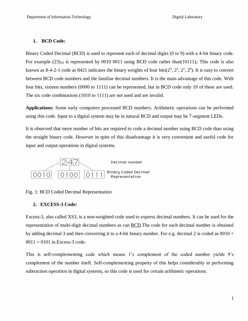
Department of Information Technology Digital Laboratory
1
1 BCD Code
Binary Coded Decimal (BCD) is used to represent each of decimal digits (0 to 9) with a 4-bit binary code
For example (23)10 is represented by 0010 0011 using BCD code rather than(10111)2 This code is also
known as 8-4-2-1 code as 8421 indicates the binary weights of four bits(23 22 21 20) It is easy to convert
between BCD code numbers and the familiar decimal numbers It is the main advantage of this code With
four bits sixteen numbers (0000 to 1111) can be represented but in BCD code only 10 of these are used
The six code combinations (1010 to 1111) are not used and are invalid
Applications Some early computers processed BCD numbers Arithmetic operations can be performed
using this code Input to a digital system may be in natural BCD and output may be 7-segment LEDs
It is observed that more number of bits are required to code a decimal number using BCD code than using
the straight binary code However in spite of this disadvantage it is very convenient and useful code for
input and output operations in digital systems
Fig 1 BCD Coded Decimal Representation
2 EXCESS-3 Code
Excess-3 also called XS3 is a non-weighted code used to express decimal numbers It can be used for the
representation of multi-digit decimal numbers as can BCDThe code for each decimal number is obtained
by adding decimal 3 and then converting it to a 4-bit binary number For eg decimal 2 is coded as 0010 +
0011 = 0101 in Excess-3 code
This is self-complementing code which means 1rsquos complement of the coded number yields 9rsquos
complement of the number itself Self-complementing property of this helps considerably in performing
subtraction operation in digital systems so this code is used for certain arithmetic operations
Department of Information Technology Digital Laboratory
2
BCD To Excess ndash 3 Code Conversions
Convert BCD 2 i e 0010 to Excess ndash 3 code
For converting 4 bit BCD code to Excess ndash 3 add 0011 i e decimal 3 to the respective code using rules of
binary addition
0010 + 0011 = 0101 ndash Excess ndash 3 code for BCD 2
Excess ndash 3 Code To BCD Conversion
The 4 bit Excess-3 coded digit can be converted into BCD code by subtracting decimal value 3 ie 0011
from 4 bit Excess-3 digit
eg Convert 4-bit Excess-3 value 0101 to equivalent BCD code
0101-0011= 0010- BCD for 2
A BCD To Excess-3 Code Conversion
Step 1 Truth Table
INPUT (BCD CODE) OUTPUT (EXCESS-3 CODE)
B3 B2 B1 B0 E3 E2 E1 E0
0 0 0 0 0 0 1 1
0 0 0 1 0 1 0 0
0 0 1 0 0 1 0 1
0 0 1 1 0 1 1 0
0 1 0 0 0 1 1 1
0 1 0 1 1 0 0 0
0 1 1 0 1 0 0 1
0 1 1 1 1 0 1 0
1 0 0 0 1 0 1 1
1 0 0 1 1 1 0 0
Department of Information Technology Digital Laboratory
3
Step 2 K-Map For Reduced Boolean Expressions Of Each Output
Fig 2 K-Map for Reduced Boolean Expressions Of Each Output (Excess-3 Code)
Department of Information Technology Digital Laboratory
4
Step3 Circuit Diagram Test the circuit for all possible combinations of input and output codes
4) Hardware Requirements Table
Table 1 Hardware Requirement Table
GATE Quantity
IC Quantity
XOR 1 7486 1
NOT 4 7404 1
AND 4 7408 1
OR 3 7432 1
Department of Information Technology Digital Laboratory
5
B Excess-3 To BCD Conversion
1 Truth Table
INPUT (EXCESS-3 CODE) OUTPUT (BCD CODE)
E3 E2 E1 E0 B3 B2 B1 B0
0 0 0 0 X X X X
0 0 0 1 X X X X
0 0 1 0 X X X X
0 0 1 1 0 0 0 0
0 1 0 0 0 0 0 1
0 1 0 1 0 0 1 01O6
51
0 1 1 0 0 0 1 1
0 1 1 1 0 1 0 0
1 0 0 0 0 1 0 1
1 0 0 1 0 1 1 0
1 0 1 0 0 1 1 1
1 0 1 1 1 0 0 0
1 1 0 0 1 0 0 1
1 1 0 1 X X X X
1 1 1 0 X X X X
1 1 1 1 X X X X
Department of Information Technology Digital Laboratory
6
2) K-Map For Reduced Boolean Expressions Of Each Output
Fig 5 K-Map For Reduced Boolean Expressions Of Each Output (BCD Code)
Department of Information Technology Digital Laboratory
7
3) Circuit Diagram Test the circuit for all possible combinations of input and output codes
4) Hardware Requirements Table
Table 2 Hardware Requirement Table
GATE Quantity
IC Quantity
XOR 1 7486 1
NOT 3 7404 1
AND 8 7408 2
OR 3 7432 1
Pin Diagrams
Department of Information Technology Digital Laboratory
8
7400 Quad 2-Input NAND Gate
7402 Quad 2-Input NOR Gate
7404 Not Gates
7408 Quad 2-Input AND Gates
7432 Quad 2-Input OR Gate
7486 Quad 2-Input Exclusive-OR Gate
Department of Information Technology Digital Laboratory
9
Conclusion
Thus we studied different codes and their conversions including applications
The truth tables have been verified using IC 7486 7432 7408 and 7404
FAQrsquos with answers
Q1) What is the need of code converters
There is a wide variety of binary codes used in digital systems Often it is required to convert from one
code to another For example the input to a digital system may be in natural BCD and output may be 7-
segment LEDs The digital system used may be capable of processing the data in straight binary format
Therefore the data has to be converted from one type of code to another type for different purpose
Q2) What is Gray code
It is a modified binary code in which a decimal number is represented in binary form in such a way that
each Gray- Code number differs from the preceding and the succeeding number by a single bit
(eg for decimal number 5 the equivalent Gray code is 0111 and for 6 it is 0101 These two codes differ
by only one bit position i e third from the left) It is non weighted code
Q3) What is the significance of Gray code
Important feature of Gray code is it exhibits only a single bit change from one code word to the next in
sequence Whereas by using binary code there is a possibility of change of all bits if we move from one
number to other in sequence (eg binary code for 7 is 0111 and for 8 it is 1000) Therefore it is more
useful to use Gray code in some applications than binary code
Q4) What are applications of Gray code
1 Important feature of Gray code is it exhibits only a single bit change from one code word to the next in
sequence This property is important in many applications such as Shaft encoders where error
susceptibility increases with number of bit changes between adjacent numbers in sequence
2 It is sometimes convenient to use the Gray code to represent the digital data converted from the analog
data (Outputs of ADC)
3 Gray codes are used in angle-measuring devices in preference to straight forward binary encoding
Department of Information Technology Digital Laboratory
10
4 Gray codes are widely used in K-map
Q5) What are weighted codes and non-weighted codes
In weighted codes each digit position of number represents a specific weight The codes 8421 2421 and
5211 are weighted codes Non weighted codes are not assigned with any weight to each digit position ie
each digit position within the number is not assigned a fixed value Gray code Excess-3 code are non-
weighted code
Q6) Why is Excess-3 code called as self-complementing code
Excess-3 code is called self-complementing code because 9rsquos complement of a coded number can be
obtained by just complementing each bit
Q7) What is invalid BCD
With four bits sixteen numbers (0000 to 1111) can be represented but in BCD code only 10 of these are
used as decimal numbers have only 10 digits fro 0 to 9 The six code combinations (1010 to 1111) are not
used and are invalid
Department of Information Technology Digital Laboratory
11
Regularity Content Viva-voce Timely
Submission Total
Dated Sign of
Subject
Teacher
2 4 2 2 10
Date of Performance Date of Completion
-------------------------------------------------------------------------------------------------------------------
Assignment No 2
------------------------------------------------------------------------------------------------------------------
Title BCD amp Excess 3 Adder
------------------------------------------------------------------------------------------------------------------
Objective 1 To study the BCD arithmetic rules
2 Comparison between binary and BCD codes
Problem Statement Design (truth table K-map) and implementation of 4-bit BCD to Excess-3 and
Excess-3 to BCD Code converters
-----------------------------------------------------------------------------------------------------------------
Hardware Requirement
i) IC 7483 (4 bit Binary adder) IC 7404(Hex INV) 7432 (OR-gate) 7408 (AND-gate)
ii) 7486 (EX-OR gate)
iii) Digital Trainer Kit -1
iv) Patch cords
----------------------------------------------------------------------------------------------------------------
Software Requirement Digital Work 30
------------------------------------------------------------------------------------------------------------------
Theory
BCD-Binary coded decimal-In this code each decimal digit represent by a 4-bit binary no BCD is a
way to express each of the decimal digits with binary code Positional weights associated to the binary bits
in BCD code are (MSB) 8-4-2-1(LSB)
BCD number 0 to 9 but greater than 9 is invalid BCD
Department of Information Technology Digital Laboratory
12
So Convert in valid BCD using add 6 ie (0110)
BCD Adder
BCD adder is a circuit that adds two BCD digits amp produces a sum of digits also in BCD
Rules for BCD addition
1 Add two numbers using rules of Binary addition
2 If the 4 bit sum is greater than 9 or if carry is generated then the sum is invalid To correct the sum
add 0110 i e (6)10 to sum If carry is generated from this addition add it to next higher order BCD
digit
3 If the 4 bit sum is less than 9 or equal to 9 then sum is in proper form
CASE I Sum lt= 9 amp carry = 0
Add BCD digits 3 amp 4
1 0 0 1 1
+ 0 1 0 0
------------
0 1 1 1
Answer is valid BCD number = (7)BCDamp so 0110 is not added
CASE II Sum gt 9 amp carry = 0
Add BCD digits 6 amp 5
1 0 1 1 0
+ 0 1 0 1
-----------
10 1 1
Department of Information Technology Digital Laboratory
13
Invalid BCD (since sum gt 9) so 0110 is to be added
2 1 0 1 1
+ 0 1 1 0
-----------
1 0 0 0 1
(1 1)BCD
Valid BCD result = (11) BCD
CASE III Sum lt = 9 amp carry = 1
Add BCD digits 9 amp 9
1 1 0 0 1
+1 0 0 1
-----------
1 0 0 1 0
Invalid BCD ( since Carry = 1 ) so 0110 is to be added
2 1 0 0 1 0
+ 0 1 1 0
------------
1 1 0 0 0
(1 8)BCD
Valid BCD result = (18) BCD
Design of BCD adder
1 To execute first step i e binary addition of two 4 bit numbers we will use IC 7483
( withCin = 0 ) which is 4 bit binary adder
2 We need to design a digital circuit which will sense sum amp carry of IC 7483 amp if sum exceeds 9 or
carry = 1 this digital circuit will produce high output otherwise its output will be zero
Circuit to check invalid BCD
Department of Information Technology Digital Laboratory
14
First we will design circuit to check sum amp then we will logically OR output of this circuit to carry
output of IC 7483
For digital circuit which we are going to design we will have 4 inputs
( S3 S2 S1 S0) amp only 1 output Y
a) Y output of this circuit Will be ORed with carry output of first adder IC
7483
b) If BCD result is invalid i e sum output of first 7483 we have to add
(6)10 ie (0110)2 that means we need one more binary adder IC 7483
c) If BCD result is valid ( ie final output of the circuit to check validity is 0) we will make an
arrangement that second adder IC 7483 adds (0)10 i e ( 0000 )2 to the sum of the first adder IC 7483
The output of the combinational circuit is used as final output carry amp carry output of second adder IC is
ignored
i ) Truth Table for design of combinational circuit for BCD adder to check invalid
BCD
K-map for output- Y=S3S2+S3S1
Department of Information Technology Digital Laboratory
15
iii) Circuit diagram
v) Hardware Requirements
GATE Quantity
IC Quantity
Binary adder 2 7483 2
AND 2 7408 1
OR 2 7432 1
B ) Design and Implement single digit EXCESS-3 adder using IC 7483
Excess-3 code is a non weighted code It is a modified form of a BCD code The Excess-3 code can be
derived from the natural BCD code by adding 3 to each coded number It is also known as Self
Complementary code
Excess-3 code is a self complementary code because 1rsquos complement of Excess-3 number is Excess-3
code for the 9rsquos complement of corresponding number
Output of BCD adder
Department of Information Technology Digital Laboratory
16
Eg Excess-3 code for (4)10 is (0111)XS-3 1rsquos complement of this number is 1000 which is Excess-3 code
for (5)10and 5 is 9rsquos complement of (4)10
Rules for Excess-3 addition
i Add two Exceess-3 numbers
ii If carry is 1 add 3 to Sum
iii If carry is 0 subtract 3 from sum
Eg (8)10 + (6)10
(8)10 = 1011 (Excess-3 for 8)
(6)10= 1001 (Excess-3 for 6)
_______________
1 0100
0011 0011
_______________
0100 0111 ( Excess 3 code for (14)10
(i)Design
1) 4 bit Binary addition of excess 3 codes of two operands can be implemented with IC 7483
2) We have to design the circuit which will either add 0011 or subtract 0011 ie add 1101 (2rsquos
complement of 0011)depending upon carry bit
Letrsquos compare 0011 and 1101
B3 B2 B1 B0
0 0 1 1 ------- When carry is 1
1 1 0 1 ------- When carry is 0
Here B0 bit in both situation is High
Now compare B3 B2 and B1 It is complement of each other
When carry is 1 Bit B1 =1 B2=B3=0
When carry is 0 Bit B1 =0 B2=B3=1
B1 bit follows the carry and B2 and B3 bit complements the carry
(ii) Circuit Diagram
Department of Information Technology Digital Laboratory
17
(iii ) HARDWARE REQUIREMENTS
Sl No IC Description Quantity
1 7404 Not Gate 01
2 7483 4 bit Binary Adder 04
CONCLUSION
BCD adder ampsubtractor is designed amp tested for all possible combinations
FAQrsquos
1 Explain and Write the significance of BCD number system
2 Write the applications of BCD amp Excess 3 code
3 Explain the rules of BCD amp Excess 3 arithmetic
4 What is the difference between BCD and binary codes
5 What do you mean by unpacked and packed BCD nos
Department of Information Technology Digital Laboratory
18
Regularity Content Viva-voce Timely
Submission Total
Dated Sign of
Subject
Teacher
2 4 2 2 10
+
Date of Performance Date of Completion
-------------------------------------------------------------------------------------------------------------------
Assignment No 3
---------------------------------------------------------------------------------------------------------------------------
Title Implementation of logic functions
----------------------------------------------------------------------------------------------------------------------
Objective 1 To study the difference between multiplexer demultiplexer and decoder
2To study the applications of multiplexer
---------------------------------------------------------------------------------------------------------------------
Problem Statement Implement of Logic function using multiplexer IC 74153
---------------------------------------------------------------------------------------------------------------------
Hardware Requirement
i) IC 74153 74138 7404 7432
ii) Digital Trainer Kit -1
iii) Patch cords
----------------------------------------------------------------------------------------------------------------
Software Requirement Digital Work 30
------------------------------------------------------------------------------------------------------------------
Theory
D CWigital Multiplexer
Multiplexer are combinational digital circuits equating as controlled switches with several data inputs (I0
I1 I2 hellip) amp one single data output (ldquooutrdquo)At any time one of the Ip is transmitted to output According to
binary signals applied on control pairs to circuit Usually the number of data inputs is a power of two
Multiplexing is the process of transmitting a large no of information units over a small no of channel
digital multiplexer is a combinational large circuit which performs the operation of multiplexing It selects
Department of Information Technology Digital Laboratory
19
the operation of multiplexing It selects the operation of binary information from one of the many input
lines amp transfer to a single op line Multiplexer is called a data selector or multiposition switch because it
selects one of the many input Selection of a particular line is controlled by a set of a selection lines or
selects inputs The number of select lines depends upon no of input lines Generally there
is lsquonrsquo selects line for lsquomrsquo input lines By applying a particular code on select lines is transmitted on the
output linesBlock diagram of MUX is shown at contains lsquo2mrsquo input lines lsquomrsquo select Such that 2m = n amp
one unable input which is used to activate or dedicate MUX Depending upon the no of IP amp OP lines
various types of multiplexers are available We have 21 41 81 161 MUX Here the first no indicates
the no of input lines amp second no indicates the no of output lines
E is called as enable input which is generally active low
Fig-Block diagram for N1 Multiplxer
Demultiplexer
Demultiplexer is a logic used to perform exactly reverse function performed by multiplexer It accepts a
single input and distributes among several outputs The selection of a particular output line is controlled
by a set of selection line There are n input lines amp 2m is the number of selection line whose bit
combinations determine which output to be selected
Encoder amp Decoder
1 Encoders are used to encode given digital number into different numbering format like
decimal to BCD Encoder Octal to Binary
2 Decoders are used to decode a coded binary word like BCD to seven segment decoder
3 Thus encoder and decoder are application specific logic develop we can not use any type of
input for any encoder and decoder
Smhelliphellips1 s0
Output(Y)
D0
D1
D2
D3
Dn
N1
multiplxer
E
Department of Information Technology Digital Laboratory
20
4 Need to select input according to encoder and decoder being selected for a particular
application as mention in examples above
Uses of Mux
1 Use for Boolean function implementation
2 Construct a common bus system
3 To select between multiple sources amp signal destination
4 Inter register transfer
Advantages
1) Simplification of logic expression not required
2) Logic design is simplified
Disadvantage
Only one function can be implemented using one MUX Hence they canrsquot be used in
combinational logic circuit which contains many function
Part-A (IC 74153)
1 VERIFICATION OF IC 74153
IC 74153 is a dual layer 41 MUX It has four input lines for (I0D-I3D) for second MUX amp active high
output lsquoYarsquo lsquoYbrsquo (1Y or 2Y) It has select lines S1S0 common to both MUX The Enable inputs are
active low EaampEb(1G and 2G) The MUX is activated when they are at logic o
Pin out of IC 74153
Department of Information Technology Digital Laboratory
21
Function table of IC 74153 (X= Donrsquot Care Condition)
Select Input
Inputs (I or II) Output
S1 S0 E (I or II) D0 D1 D2 D3 Y
X X 1 X X X X 0
0 0 0 0 X X X 0
0 0 0 1 X X X 1
0 1 0 X 0 X X 0
0 1 0 X 1 X X 1
1 0 0 X X 0 X 0
1 0 0 X X 1 X 1
1 1 0 X X X 0 0
1 1 0 X X X 1 1
2CASCADING OF IC 74153
Cascading is done to expand two or more MUX ICrsquos to a digital multiplexer with larger no of inputs ie
multiplexer stocks or tress is designed The enable input is used for cascading In case of IC 74153 we
have only two select lines But for certain application 3 select lines are required then it can be
obtained by cascading using enable Now with 3 select lines we have 8 combinations Out of this
combination the MSB is O MSB is 1 for last four combination so we can use these MSB to select
any 1 MUX out of two by connecting it to E pin of first 41 MUX
Function table of IC 74153 as 8 1 Mux by cascading 2 41 Mux
Select Input Output
C (1G 2G ) B (S1) A (S0) Y
0 0 0 D0
0 0 1 D1
0 1 0 D2
0 1 1 D3
1 0 0 D4
1 0 1 D5
Department of Information Technology Digital Laboratory
22
1 1 0 D6
1 1 1 D7
3FUNCTION IMPLEMENTATION
Y= sum m (1 3 5 6)
Thisexpression is in Standard SOP form and it is three variable function So we need to use mux with
three select inputs ie 81 Mux Already we have implemented 81 Mux using IC 74153 For Boolean
function in Standard SOP form we connect data inputs corresponding to the minterms present in the given
function to Vcc and remaining data inputs to ground
Truth table
Inputs Output
C B A Y
0 0 0 0
0 0 1 1
0 1 0 0
0 1 1 1
1 0 0 0
1 0 1 1
1 1 0 1
1 1 1 0
LOGIC DIAGRAM
Hardware Requirements
GATE Quantity
IC Quantity
Mux 1 74153 1
NOT 1 7404 1
OR 1 7432 1
Department of Information Technology Digital Laboratory
23
Part-B Decoder (IC 74138)
Theory
Discrete quantities of information are requested in digital system with binary codes A binary code of n
bits is capable of representing into 2n distinct elements of the coded information
Decoder converts coded input to coded outputs accepts one of the code
There are different types of decoders such as 38 decoder 416 line decoders etc These are in general
called as n m line decoder where m=2n and n= no of input lines and m=no of output lines Demux also
takes one input data line source and selectively distributes it to one of n output channels The only
difference between demux and decoder is that demux has Din (data ip) line whereas decoder does not
have
ADVANTAGES
1) The decoder provides best implementation whenever there are many outputs of the combinational
circuit and each op of the function (or its complement) is required to be expressed with a small no
of minterms
2) The decoder can function as demux If the Enable ip line is taken as Din (data ip)
DISADVANTAGES
Since decoder method requires an OR gate for each op function so there is new hardware used And it is
always advisable to use minimum hardware as we come across problems like propagation delay of gates
APPLICATIONS
Decoder is worthily used for decoding binary information and memory interfacing It is used for the
implementation of Boolean function
Differentiate between Mux Demux Decoder
Point Multiplexer Demultiplexer Decoder
Input Many input lines Single input line Many input line also Acts as select line
Output Single output line Many output line Many output lineActive low output
Select line 2m = n n = 2m Enable inputs used
Department of Information Technology Digital Laboratory
24
A) Verification of IC 74138
We use IC 74138 which accepts 3 binary weighted inputs (A0 A1 A2) and when enabled provides
mutually exclusive active low outputs (y0-y7) It features 3 Enable ips Two active low (G2A G2B) and
one active high (G1) Every output will be high unless G2A G2Bare low and G1 is high It has
demultiplexing capability and multiple enable ips for easy expansion
IC Diagram
Function Table of 38 decoder
Input Output
Enable Data
G2A G2B G1 A2 A1 A0 Y0 Y1 Y2 Y3 Y4 Y5 Y6 Y7
0 0 0 X X X 1 1 1 1 1 1 1 1
0 1 1 X X X 1 1 1 1 1 1 1 1
1 0 1 X X X 1 1 1 1 1 1 1 1
1 1 1 X X X 1 1 1 1 1 1 1 1
Department of Information Technology Digital Laboratory
25
0 0 1 0 0 0 0 1 1 1 1 1 1 1
0 0 1 0 0 1 1 0 1 1 1 1 1 1
0 0 1 0 1 0 1 1 0 1 1 1 1 1
0 0 1 0 1 1 1 1 1 0 1 1 1 1
0 0 1 1 0 0 1 1 1 1 0 1 1 1
0 0 1 1 0 1 1 1 1 1 1 0 1 1
0 0 1 1 1 0 1 1 1 1 1 1 0 1
0 0 1 1 1 1 1 1 1 1 1 1 1 0
B) Cascading of IC 74138
The enable ip G1 active high of IC 74138 is used for cascadingfor cascading 2 ICrsquos the enable ip G1 of
first IC is connected to G1 enable ip of second IC through a NOT gate This enable ip is used as MSB
select ip line A3 the other three select input lines of both ICrsquos (A0A1A2) are also shorted to select
input lines of second IC to get single ip select lines (A0A1A2)
The ip line A3 is used to enable disable the 2 IC 74138 decoders When A3=0 first IC is enabled and
second is disabled Thus the first decoder will generate minterms from 0000 to 0111 as op and the second
decoder will generate nothing When A3=1 the enable conditions are reversed and thus second decoder
IC will generate minterms 1000 to 1111
Function Table of 416 decoder using IC 74138 (38 decoder)
Input Output
Enable Data
G2
A
G2
B
A
3
A
2
A
1
A
0
Y
0
Y
1
Y
2
Y
3
Y
4
Y
5
Y
6
Y
7
Y
8
Y
9
Y1
0
Y1
1
Y1
2
Y1
3
Y1
4
Y1
5
0 1 X X X X 1 1 1 1 1 1 1 1 1 1 1 1 1 1 1 1
Department of Information Technology Digital Laboratory
26
1 0 X X X X 1 1 1 1 1 1 1 1 1 1 1 1 1 1 1 1
1 1 X X X X 1 1 1 1 1 1 1 1 1 1 1 1 1 1 1 1
0 0 0 0 0 0 0 1 1 1 1 1 1 1 1 1 1 1 1 1 1 1
0 0 0 0 0 1 1 0 1 1 1 1 1 1 1 1 1 1 1 1 1 1
0 0 0 0 1 0 1 1 0 1 1 1 1 1 1 1 1 1 1 1 1 1
0 0 0 0 1 1 1 1 1 0 1 1 1 1 1 1 1 1 1 1 1 1
0 0 0 1 0 0 1 1 1 1 0 1 1 1 1 1 1 1 1 1 1 1
0 0 0 1 0 1 1 1 1 1 1 0 1 1 1 1 1 1 1 1 1 1
0 0 0 1 1 0 1 1 1 1 1 1 0 1 1 1 1 1 1 1 1 1
0 0 0 1 1 1 1 1 1 1 1 1 1 0 1 1 1 1 1 1 1 1
0 0 1 0 0 0 1 1 1 1 1 1 1 1 0 1 1 1 1 1 1 1
0 0 1 0 0 1 1 1 1 1 1 1 1 1 1 0 1 1 1 1 1 1
0 0 1 0 1 0 1 1 1 1 1 1 1 1 1 1 0 1 1 1 1 1
0 0 1 0 1 1 1 1 1 1 1 1 1 1 1 1 1 0 1 1 1 1
0 0 1 1 0 0 1 1 1 1 1 1 1 1 1 1 1 1 0 1 1 1
0 0 1 1 0 1 1 1 1 1 1 1 1 1 1 1 1 1 1 0 1 1
0 0 1 1 1 0 1 1 1 1 1 1 1 1 1 1 1 1 1 1 0 1
0 0 1 1 1 1 1 1 1 1 1 1 1 1 1 1 1 1 1 1 1 0
C) Implementation of Boolean function
The procedure for implementation of combinational circuit by means of a decoder and lsquoORrsquo gates requires
that the Boolean function fir the circuit be expressed in Sum of Minterms These forms can be obtained by
Department of Information Technology Digital Laboratory
27
expanding the function A decoder is then chosen which generates all the minterms of n ip variables The
ip to each OR gate are selected from the decoder outputs according to the minterms list in each function
i) F1=summ (1 3 5 7)
Truth table
Logic Diagram
ii) F2=summ (1 3 5 7111315)
Truth table
Logic Diagram
Conclusion In this way multiplexer Decoderamp its applications are studied implemented amp
tested
FAQrsquos
1What is a multiplexer
2What is a Demultiplexer
3 Enlist applications of multiplexer
Department of Information Technology Digital Laboratory
28
Regularity Content Viva-voce Timely
Submission Total
Dated Sign of
Subject
Teacher
2 4 2 2 10
Date of Performance Date of Completion
-------------------------------------------------------------------------------------------------------------------
Assignment No4
------------------------------------------------------------------------------------------------------------------
Title 3 bit updown Asynchronous and Synchronous counter using IC7476
------------------------------------------------------------------------------------------------------------------
Objective To understand design procedure of asynchronousamp Synchronous counter
------------------------------------------------------------------------------------------------------------------
Problem Statement Design (State diagram state table amp K map) and implementation of 3
bit Up and Down Asynchronous and Synchronous Counter using master slave JK flip-flop IC 7476
-----------------------------------------------------------------------------------------------------------------
Hardware Requirement
i) IC 7476 (MS-JK Flip-flop) IC 7408(Quad 2 ip AND Gate)
IC 7432 (Quad 2 ip OR Gate) and IC 7404 (Hex Inverter)
ii) Digital Trainer Kit -132
iii) Patch cords
----------------------------------------------------------------------------------------------------------------
Software Requirement Digital Work 30
------------------------------------------------------------------------------------------------------------------
Theory
Counters counters are logical device or registers capable of counting the no of states or no of clock
pulses arriving at its clock input where clock is a timing parameter arriving at regular intervals of time
so counters can be also used to measure time amp frequencies They are made up of flip flops Where the
Department of Information Technology Digital Laboratory
29
pulse are counted to be made of it goes up step by step amp the op of counter in the flip flop is decoded to
read the count to its starting step after counting n pulse incase of module counters
Types of Counters
Counter are of two types
1) Asynchronous counter
2) Synchronous counter
Asynchronous counter
A digital counter is a set of flip flop The flip flop are connected such that their combined state at any time
is binary equivalent of total no of pulses that have occurred up to that time Thus its name implies a
counter is used to count pulse A counter is used as frequency dividers To obtain waveform with
frequency that is specific fraction of clock frequency
Counter may be Asynchronous or synchronous The Asynchronous counter is also called as ripple counter
An Asynchronous counter uses T flip flop to perform a counting function The actual hardware used is
usually J-K flip flop with J amp K connected to logic1Even D flip flops may be used here
In asynchronous counter commonly called ripple counter the first flip-flop is clocked by the external
clock pulse amp then each successive flip-flop is clocked by the Q or Qrsquo output of the previous flip-flop
Therefore in an asynchronous counter the flip-floprsquos are not clocked simultaneously The input of MS-JK
is connected to VCC because when both inputs are one output is toggled As MS-JK is negative edge
triggered at each high to low transition the next flip-flop is triggered
Synchronous Counter
When counter is clocked such that each flip flop in the counter is
triggered at the same time the counter is called as synchronous counter
The gates propagation delay at reset time will not be present or we may say will not occur
1) Asynchronous Up Counter
Fig 1 shows 3bit Asynchronous Up Counter Here Flip-flop 2 act as a MSB Flip-flop and Flip-flop 0 act
as a LSB Flip-flop Clock pulse is connected to the Clock of Flip-flop 0 Output of Flip-flop 0(Q0) is
connected to clock of next flip-flop (ie Flip-flop 1) and so on As soon as clock pulse changes output is
going to change (at the negative edge of clock pulse) as a Up count sequence For 3 bit Up counter state
table is as shown below
Department of Information Technology Digital Laboratory
30
State Table
Logic diagram
Fig 1 3 Bit Asynchronous Up Counter
Hardware requirements
Gate
Flip flop
Quantity IC Quantity
MS JK 3 7476 2
2) Down Counter
Fig 2 shows 2 bit Asynchronous Down Counter Here Flip-flop 2 act as a MSB Flip-flop and Flip-flop 0
act as a LSB Flip-flop Clock pulse is connected to the Clock of Flip-flop 0 Output of Flip-flop 0 (Q0rsquo) is
Counter States Count
Q2 Q1 Q0
0 0 0 0
1 0 0 1
2 0 1 0
3 0 1 1
4 1 0 0
5 1 0 1
6 1 1 0
7 1 1 1
8 0 0 0
Department of Information Technology Digital Laboratory
31
connected to clock of next flip-flop (ie Flip-flop 1) and so on As soon as clock pulse changes output is
going to change (at the negative edge of clock pulse) as a down count sequence For 3 bit down counter
sate table is as shown below
In both the counters Inputs J and K are connected to Vcc hence J-K Flip flop work in toggle mode Preset
and Clear both are connected to logic 1
State Table
Logic diagram
Fig 2 3 Bit Asynchronous Down Counter
Hardware requirements
Counter States Count
Q2 Q1 Q0
7 1 1 1
6 1 1 0
5 1 0 1
4 1 0 0
3 0 1 1
2 0 1 0
1 0 0 1
0 0 0 0
7 1 1 1
Department of Information Technology Digital Laboratory
32
Gate
Flip flop
Quantity IC Quantity
MS JK 3 7476 2
Applications
The asynchronous counters are specially used as the counting devices
They are also used to count number of pulses applied
It also works as frequency divider
It helps in counting the number of product coming out of the machinery where product is coming out at
equal interval of time
Types of synchronous counter
1) Up counter
2) Down counter
1 3 bit Synchronous up counter
The up counter counts from 0 to7 ie(000 to 111)for this we are using MS JK flip flop In IC 74LS76 2
MS J-K flip flops are present The clock pulse is given at pin 1 amp 6 of the 1st IC amp pin 1 of 2nd IC Next
state decoder logic is designed with the help of state table
State table for synchronous up counter
Present state Next state Flip flop 3 Flip flop 2 flip flop 1
Q2 Q1 Q0 Q2 Q2 Q0 J2 K2 J1 K1 J0 K0
0 0 0 0 0 1 0 x 0 X 1 x
0 0 1 0 1 0 0 x 1 X x 1
0 1 0 0 1 1 0 x x 0 1 x
0 1 1 1 0 0 1 x x 1 x 1
1 0 0 1 0 1 x 0 0 X 1 X
1 0 1 1 1 0 x 0 1 X x 1
1 1 0 1 1 1 x 0 x 0 1 X
1 1 1 0 0 0 x 1 x 1 x 1
Department of Information Technology Digital Laboratory
33
K-Map
Q1Q0
Q2
00 01 11 10
0 0 0 1 0
1 X X X X
J2= Q1Q0
Q1Q0
Q2
00 01 11 10
0 X X X X
1 0 0 1 0
K2= Q1Q0
Q1Q0
Q2
00 01 11 10
0 0 1 X X
1 0 1 X X
J1= Q0
Q1Q0
Q2
00 01 11 10
0 X X 1 0
1 X X 1 0
K1= Q0
Department of Information Technology Digital Laboratory
34
Q1Q0
Q2
00 01 11 10
0 1 X X 1
1 1 X X 1
J0= 1
Q1Q0
Q2
00 01 11 10
0 X 1 1 X
1 X 1 1 X
K0= 1
Logic Diagram
Fig 1 3 bit Synchronous up counter
Department of Information Technology Digital Laboratory
35
2 3 bit Synchronous down counter
This is used to count from 7-0 ie(111-000)for this also 2 ICrsquos of 74LS76 are required amp hence we use 3
MS JK flip flops Here also clock is given to 1stamp 6th pin of 1st IC amp1st pin of 2nd IC enabling to apply
clock to all flip flop at a time Next state decoder logic is designed with the help of state table
State table for synchronous down counter
Present state Next state Flip flop 3 Flip flop 2 Flip flop 1
Q2 Q1 Q0 Q2 Q1 Q0 J2 K2 J1 K1 J0 K0
1 1 1 1 1 0 X 0 X 0 X 1
1 1 0 1 0 1 X 0 X 1 1 X
1 0 1 1 0 0 X 0 0 X X 1
1 0 0 0 1 1 X 1 1 X 1 X
0 1 1 0 1 0 0 X X 0 X 1
0 1 0 0 0 1 0 X X 1 1 X
0 0 1 0 0 0 0 X 0 X X 1
0 0 0 1 1 1 1 X 1 X 1 X
K-Map
Q1Q0
Q2
00 01 11 10
0 1 0 0 0
1 X X X X
J2= Q1Q0
Q1Q0
Q2
00 01 11 10
Department of Information Technology Digital Laboratory
36
0 X X X X
1 1 0 0 0
K2= Q1Q0
Q1Q0
Q2
00 01 11 10
0 1 0 X X
1 1 0 X X
J1= Q0
Q1Q0
Q2
00 01 11 10
0 X X 0 1
1 X X 0 1
K1= Q0
Q1Q0
Q2
00 01 11 10
0 1 X X 1
1 1 X X 1
J0= 1
Q1Q0
Q2
00 01 11 10
0 X 1 1 X
1 X 1 1 X
K0= 1
Department of Information Technology Digital Laboratory
37
Logic Diagram
Fig 2 3 bit Synchronous down counter
Uses
1 Specially used as the counting devices
2 Used in frequency divider circuit
3 Used in digital voltmeter
4 Used in counter type A to D converter
5 Used for time measurement
6 It helps in counting the no of product coming out from machinery where product is coming out
at equal interval of time
Conclusion
Up and down counters are successfully implemented the counters are studied amp op are checked The
state table is verified
PRACTICE ASSIGNMENTS EXERCISE MODIFICATIONS
1 Design amp implement 2 bit controlled synchronous counter
2 Designamp implement 4 bit controlled synchronous counter
3 Designamp implement truncated synchronous up or down counter
FAQrsquos with answers
1 What do you mean by Counter
A Counter is a register capable of counting the no of clock pulses arriving at its
clock inputs Count represents the no of clock pulses arrived A specified
sequence of states appears as the counter output
Department of Information Technology Digital Laboratory
38
2 What are the types of Counters Explain each
There are two types of counters as Asynchronous Counter and Synchronous Counter
Asynchronous Counter In this counter the first flip-flop is clocked by the external clock pulse
and then each successive flip-flop is clocked by the Q or Qrsquo op of the previous flip-flop Hence in
Asynchronous Counter flip-flops are not clocked simultaneously and hence called as Ripple
Counter Synchronous Counter In this counter the common clock input is connected to all the
flip-flops simultaneously
3 What do you mean by pre-settable counters
A counter in which starting state is not zero can be designed by making use of the
preset inputs of the flip flops This is referred to as loading the counter
asynchronously This is referred to as pre-settable counter
4 What are the applications of synchronous counters
Digital clock
Frequency divider circuits
Frequency counters
Used in analog to digital converters
5 What are the advantages of synchronous counters over asynchronous counters
Propagation delay time is reduced
Can operate at a much higher frequency than the asynchronous counters
6 Ring counter is an example of synchronous counters or asynchronous counter
Synchronous counter Since all the flip flops are clocked simultaneously
7 Twisted Ring (Johnsonrsquos) counter is an example of synchronous counters or asynchronous
counter
Synchronous counter Since all the flip flops are clocked simultaneously
8 What is the difference between ring counter and twisted ring counter
In ring counter pulses to be counted are applied to a counter it goes from state to state and the
output of the flip flop s in the counter is decoded to read the count Here the uncomplimentary
output (Q) of last flip flop is fed back as an input to first flip flop Ring counters are referred as
MOD lsquoNrsquo counters
Department of Information Technology Digital Laboratory
39
But in Twisted ring counter the complimentary output (Q bar) of last flip flop is fed back as an
input to first flip flop Twisted Ring counters are referred as MOD lsquo2Nrsquo counters
9 What are the applications of ring counters
Ring counter outputs are sequential non-overlapping pulses which are useful for control state
counters Used in stepper motor this requires pulses to rotate it from one position to the next Used
as divide by lsquoNrsquo ((MOD lsquoNrsquo) counters
10 What are the applications of ring counter twisted ring counters
Used as divide by lsquo2Nrsquo ((MOD lsquo2Nrsquo) counters
Used for control state counters
Used for generation of multiphase clock
11 List the Synchronous Counter ICs
IC 74160 Decade Up Counter
IC 74161 4 bit binary Up Counter
IC 74162 Decade Up Counter
IC 74163 4 bit binary Up Counter
IC 74168 Decade UpDown Counter
IC 74169 4 bit Binary UpDown Counter
IC 74190 Decade UpDown Counter
IC 74191 4 bit Binary UpDown Counter
IC 74192 Decade UpDown Counter
IC 74193 4 bit Binary UpDown Counter
Department of Information Technology Digital Laboratory
40
Regularity Content Viva-voce Timely
Submission Total
Dated Sign of
Subject
Teacher
2 4 2 2 10
Date of Performance Date of Completion
-------------------------------------------------------------------------------------------------------------------
Assignment No 5
-------------------------------------------------------------------------------------------------------------------------------
Title Design and implementation of Module lsquonrsquo counter with IC7490 and IC 74191
-----------------------------------------------------------------------------------------------------------------------------
Objective To know difference between regular amp truncated counter as well as binary ampBCD Counter
--------------------------------------------------------------------------------------------------------------------------------
Problem Statement To design and implement mod - 10 mod ndash 7 mod - 99 asynchronous BCD
counter using IC 7490 and to design and implement up down mod - n Binary counter using IC 74191
-----------------------------------------------------------------------------------------------------------------
Hardware Requirement
i) IC 7490 IC 74191 basic gates
ii) Digital Trainer Kit -1
iii) Patch cords
----------------------------------------------------------------------------------------------------------------
Software Requirement Digital Work 30
------------------------------------------------------------------------------------------------------------------
Theory
Part A ndash IC 7490
IC 7490 is a TTL MSI (medium scale integration) decade counter It contains 4 master slave flip flops
internally connected to provide MOD-2 ie divide by 2 and MOD-5 ie divide by 5 counters MOD-2 and
Mod-5 counters can be used independently or in cascading
Department of Information Technology Digital Laboratory
41
It is a 4-bit ripple type decade counter The device consists of 4-master slave flip flops internally
connected to provide a divide by two and divide by 5 sections Each section has a separate clock ip to
initiate state changes of the counter on the high to low clock transition
Since the op from the divide by 2 section is not internally connected to the succeeding stages The device
may be operated in various counting modes In a BCD counter the CP1 input must be externally connected
to QA op The CP0ip receives the incoming count producing a BCD count sequence It is also provided
with additional gating to provide a divide by 2 counter and binary counter for which the count cycle length
is divide by 5 The device may be operated in various counting modes
There are 2 reset inputs R0(1) and R0(2) both of which need to be connected to the lsquologic 1rsquo for clearing all
flip flops Two set inputs Rg(1) and Rg(2) when connected to logic 1 are used for setting counter to 1001
(BCD 9)
Pin out of IC 7490
Fig Pin configuration of IC7490
Table 1-pin name and description of IC7490
Pin name Description
Input B This is clock input to the internal MOD-5 ripple counter which is negative
edge triggered
R0(1)R0(2) Gated zero reset inputs
Department of Information Technology Digital Laboratory
42
R9(1)R9(2) These are gated set to nine inputs
QDQCQB Output of internal MOD-5 counter with QD as MSB
QA Output of internal MOD-2 counter with QA as LSB
Input A Clock input to FF-A which is negative edge triggered
Functional Table for IC7490
Reset inputs Output
R0(1) R0(2) R9(0) R9(1) QD QC QB QA
1 1 0 X 0 0 0 0
1 1 X 0 0 0 0 0
X X 1 1 1 0 0 1
X 0 X 0 COUNTER
0 X 0 X COUNTER
0 X X 0 COUNTER
X 0 0 x COUNTER
Department of Information Technology Digital Laboratory
43
Basic internal Structure of IC 7490
Function Table of MOD-5 counter
Design of MOD-10 counter using IC 7490
The QA op the first flip flop is connected to the input B which is clock ip of internal MOD-5 ripple
counter Due to cascading of Mod-2 and Mod-5 counters the overall configuration the decade counters
count from 0000 to 1001 After 1001 mod-5 resets to 0000 and next count after 1001 is 0000
When QA op is connected to B ip we have the Mod-2 counter followed by Mod-5 counter The
count sequence obtained is shown in the table It may be noted that QA changes from 0 to 1 the state of
InputB clock Output
Count QD QC QB
0 0 0 0
0 0 1 1
0 1 0 2
0 1 1 3
1 0 0 4
Department of Information Technology Digital Laboratory
44
Mod-5 counter doesnrsquot change whereas when QA changes from 1 to 0 the Mod-5 counter goes to the next
state
Logic DiagramMOD-10 counter using IC 7490
5 Modulus n Counter
Function table
Ip clock
Output
Count QD QC QB QA
0 0 0 0 0
0 0 0 1 1
0 0 1 0 2
0 0 1 1 3
0 1 0 0 4
Department of Information Technology Digital Laboratory
45
Design of Mod-7 Counter using IC 7490
Mod-7 counter counts through seven states from 0 to 6 counters and it should reset as soon as the
count becomes 7 The op of reset logic should be 1 corresponding to invalid states The reset logic op
should be applied to pin 2 and 3
Truth Table of Reset Logic
0 1 0 1 5
0 1 1 0 6
0 1 1 1 7
1 0 0 0 8
1 0 0 1 9
QD QC QB QA Y
0 0 0 0 0
0 0 0 1 0
0 0 1 0 0
0 0 1 1 0
0 1 0 0 0
0 1 0 1 0
0 1 1 0 0
0 1 1 1 1
1 0 0 0 1
1 0 0 1 1
Department of Information Technology Digital Laboratory
46
Logic Diagram Mod 7 Counter using IC 7490
Function table
Ip clock
Output
Count QD QC QB QA
0 0 0 0 0
0 0 0 1 1
0 0 1 0 2
0 0 1 1 3
0 1 0 0 4
0 1 0 1 5
0 1 1 0 6
Department of Information Technology Digital Laboratory
47
Design of Mod-99 using IC 7490
For Mod-99 two IC 7490rsquos will be required Hence to implement a divide by 99 counter we have
to use two decade counters ICrsquos A divide by 99 counter counts 99 states from 0 to 98 and the counter
should reset as soon as the count becomes 99 So in order to reset the counter of 99 connect the Q op
which are equal to 1 in the count of 99 to an lsquoAndrsquo gate amp then connect and op to the reset ip of both
ICrsquos
MOD-100 Counter-
MOD-100 counter can be obtained by cascading two decade counter ICrsquos
Each IC gives divide by 10 counts Hence 2 ICs will give 1010=100 counts
Clock is applied to the input A of IC 7490 the Q1 output is connected to B input etc
For cascading the QD output of the first IC is connected to the input A of second IC Thus QD of
IC-(1) acts as clock input to IC-(2)
The Ro (1) Ro(2) R9(1) R9(2) inputs of both ICs are connected to ground so as to make them
inactive
The total count provided by the two counters varies from 00 to 99 decimal that means 100 states
Hence it is a MOD-10 counter
Impleacutementations
FigureMOD-100 counters using IC 7490
Department of Information Technology Digital Laboratory
48
B) IC 74191 ndash Theory
IC74191 is 4-bit binary synchronous reversible up down counter It contains 4 master slave flip flops
with internal gating and steering logic to provide asynchronous reset and synchronous count updown
operations its asynchronous parallel capability permits the counter to be preset to any desire number D0
to D3 are the parallel data inputs Information present on the parallel data inputs D0 to D3 is loaded into
the counter and appears on the output when the load PLinput is lowThisoperation overrides the counting
function Counting is inhabited by the high level on the enable G input when G input is low internal state
changes are initiated synchronously by the low to high transitions of the clock inputs the updown input
signal determines the direction of input
Function Table
Operating
mode
Inputs Outputs
PL UD G CLK Dn
Parallel
load L X X X L L
L X X X H H
Count up H L 0 uarr X Count up
Count
down H H 0 uarr X
Count
down
Hold(No
change) H X H X X No change
Pin details ndash
D0 to D3 input lines PL parallel load
G is Enable input ndash enabling the counting
Q0 to Q3 output lines
Downup determines the direction of counting
Clk clock input for counter
Terminal Count Max(1111) min(0000) For these states signal goes high for 1clock pulse
Ripple clock Clock input for next higher state
Department of Information Technology Digital Laboratory
49
Pin Diagram IC 74191
Up counter- Truth Table
Clk
Pulses QA QB QC QD
0 0 0 0 0
1 0 0 0 1
2 0 0 1 0
3 0 0 1 1
4 0 1 0 0
5 0 1 0 1
6 0 1 1 0
7 1 1 1 1
8 1 0 0 0
9 1 0 0 1
10 1 0 1 0
11 1 0 1 1
12 1 1 0 0
13 1 1 0 1
Department of Information Technology Digital Laboratory
50
14 1 1 1 0
15 1 1 1 1
Logic Diagram
Steps-
Connect the circuit as shown above
Apply clock ip to pin no14
Connect UD to GND
Verify the output according to truth table
Logic diagram of down counter
Steps-
Connect the circuit as shown above
Apply clock ip to pin no14
Connect UD to VCC
Verify the output according to truth table
UD D3 D2 D1 D0 PL
Clock IC 74191
G RC
MAX MIN
Q3 Q2 Q1 Q0 TC
vcc
NC
NC
Outputs
no connection
vcc
Department of Information Technology Digital Laboratory
51
With the help of IC74191 we can implement truncated updown counter by using following logic ndash
Connect data input line to particular count you want to load
According to requirement make Truth table
Draw the K-map
Find out Boolean expression
Draw the logic diagram and that is the combinational logic for your count and apply the output of
that circuit to PL
According to requirement we get the UP and down counting
5 Modulus n Counter
Presettable updown counter
Mod 11 counter
Implementation of presetttable mod updown counter using IC- 74LS191
1 Load Data on data lines D0 to D3 (0101)
2 Counter will go through the states from 0101 0110hellip1111 in up counter and 0101 to 0000 in
down counter
Combinational Circuit
CLOCK D3 D2 D1 D0
TC
U D 74191 RC
G PL
Updown Q3 Q2 Q1 Q0 PL
Q3 Q2 Q1 Q0
Preset Count
Department of Information Technology Digital Laboratory
52
3 The logic circuit should be designed in such a way that only when all the outputs are high output
of the reset circuit should be low and the counter should jump to state 5 It should again start
counting from 0101 to 0000
State Table
Down Counter UP Counter
IC 74191 is 4 bit counter Thus it counts 0000 to 1111 different 16 states For MOD11 counter we require
different 11 states so 5 steps must be skipped from 16 states We get MOD11 by presetting counter to
value 5
Assignment Question
Design and Implement MOD 7 MOD 10 and MOD 12 using IC 74191
FAQs
1 What do you mean modulus counter
Counter
state Clock
pulse
Q3 Q2 Q1 Q0
1 0 1 0 1
2 0 1 1 0
3 0 1 1 1
4 1 0 0 0
5 1 0 0 1
6 1 0 1 0
7 1 0 1 1
8 1 1 0 0
9 1 1 0 1
10 1 1 1 1
11 1 1 1 1
Counter state
Clock pulse
FF outputs
Q3 Q2 Q1 Q0
1 0 1 0 1
2 0 1 0 0
3 0 0 1 1
4 0 0 1 0
5 0 0 0 1
6 0 0 0 0
7 0 1 0 1
Department of Information Technology Digital Laboratory
53
It represents the number of possible states of counter
2 How will you use the 7490 IC to design symmetrical divide by 10 frequency counter
The divide by 5 circuit followed by divide by 2 circuit will give symmetrical output
3Where counters are used Give real life example of counter
Modulus n Counter
Binary counter ndash An N stage counter that recycles after 2 Ncount The count proceds in specified binary
sequence Counter Presetable- A counter which can be set to a desired value before the start of the
counting UPDown counter ndash A counter that can count in both up and down direction depending upon a
control input
Department of Information Technology Digital Laboratory
54
Regularity Content Viva-voce Timely
Submission Total
Dated Sign of
Subject
Teacher
2 4 2 2 10
Date of Performance Date of Completion
-------------------------------------------------------------------------------------------------------------------
Assignment No6
------------------------------------------------------------------------------------------------------------------
Title Sequence Generator
------------------------------------------------------------------------------------------------------------------
Objective To understand sequence generator one of the sequential circuit
-------------------------------------------------------------------------------------------------------------------
Problem Statement Design (State Diagram State Table K Map) and implementation of Sequence
Generator using Shift Register IC 74194
-----------------------------------------------------------------------------------------------------------------
Hardware Requirement
i) IC 741947408 (AND-gate) 7432 (OR-gate)
ii) Digital Trainer Kit -1
iii) Patch cords
----------------------------------------------------------------------------------------------------------------
Software Requirement Digital Work 30
------------------------------------------------------------------------------------------------------------------
Theory
Part A Sequence Generator with Flip flop
A sequential circuit which generates a prescribed sequence of bits in synchronism with a clock is referred
to as a sequence generator These pulse trains or sequence of bits can be used to open valves close gates
turn on lights and turn off machines and other variety of jobs
Department of Information Technology Digital Laboratory
55
For the design of sequence generator we first determine the required no of flip flops and the logic circuit
for the next state decoder
No of flip flops required to generate particular sequence can be determined as follows
1) Find the no of 1rsquos in the sequence
2) Find the no of 0rsquos in the sequence
3) Take the maximum out of two
4) If N is the required no of flip flops choose minimum value of lsquonrsquo to satisfy equation given below
Max (0rsquos 1rsquos) le 2n-1
The sequence generator can be classified as
1) sequence generator without bushing
2) sequence generator with bushing
The aim in this experiment is to design a sequence generator to generate a sequence of bit ie 10101
Part B Sequence Generator using Shift Register IC 74194
IC 74194 4 bit bidirectional Shift Register
This bidirectional shift register is designed to incorporate virtually all the features a system designer may
want in a shift register they feature Parallel inputs parallel outputs right shift left shift serialinputs
operating mode control inputsand a direct overriding clear line The register has four distinct modes of
operationsnamely
1 Parallel load
2 Shift right (in the direction QA towards QD)
3 Shift left (in the direction QD towards QA)
4 Inhibit clock (do nothing)
Synchronous parallel loading is accomplished by applying the four bits of data and taking both
mode control inputs S0 and S1High The data is loaded in to the associated flip-flops and appear
at the outputs after positive transition of the clock input During loading serial data flow is
inhibited
Shift right is accomplished synchronously with the rising edge of the clock pulse when S0 is High
and S1 is Low Serial data for this mode is entered at the shift right data input When S0 is Low
and S1 is High data shifts left synchronously and new data is entered at the shift left serial input
Clocking of the flip flop is inhibited when both mode control inputs are LOW
Department of Information Technology Digital Laboratory
56
Mode Control Input Operation
S1 S0
0 0 Clock Inhibit
0 1 Shift right
1 0 Shift Left
1 1 Parallel loading
Function Table of IC 74194
Design
The minimum number of flip-flops N required to generate a sequence of length S is given by S
le 2N ndash 1
In this case S=7 therefore the minimum value of N which may generate in this sequence is 3
However it is not guaranteed to lead to a solution If the given sequence leads to seven distinct
states then only three flip flops are sufficient otherwise we have to increase the number of flip
flops We write the states of circuit as given in table 1 The prescribed sequence is listed under QA
and the sequence listed under QB and QC are the same sequence delayed by one and two clock
pulses respectively From the table we observe that all the states are not distinct which means N=3
is not sufficient Next we assume that N=4 and prepare table 2 The last column gives the required
serial input for getting the desired change of state when a clock pulse is applied This is obtained
by assuming D type flip flop and looking at the QA output For example at the falling edge of first
clock pulse QA=1 The second clock pulse must result in QA=1 which requires its D input to be 1
In the same manner all the entries in column Y are determined
Table 1 State Assignment Table of Sequence Generator (N=3)
Number of Clock
Pulses
Flip Flop Inputs States
QA QB QC
1 1 1 1 7
2 1 1 1 7
3 0 1 1 3
4 1 0 1 5
Department of Information Technology Digital Laboratory
57
5 0 1 0 2
6 1 0 1 5
7 1 1 0 6
Excitation table of D Flip-Flop
Present State Qn Next State Qn+1 Flip-Flop Input D
0 0 0
0 1 1
1 0 0
1 1 1
Table 2State Assignment Table of Sequence Generator (N=4)
Number of Clock
Pulses
Flip Flop Inputs States
Y
Serial ip QA QB QC QD
1 1 1 1 0 14 1
2 1 1 1 1 15 0
3 0 1 1 1 7 1
4 1 0 1 1 11 0
5 0 1 0 1 5 1
6 1 0 1 0 10 1
7 1 1 0 1 13 1
K-Map Simplification
Department of Information Technology Digital Laboratory
58
00 01 11 10
00 X X X X
01 X 1 1 X
11 X 1 0 1
10 X X 0 1
Y= QArsquo + QBrsquo + QCrsquo = QAQBQC
LOGIC DIAGRAM
HARDWARE REQUIREMENTS
Sr no ICs Description Quantity
11 74194 4 bit bidirectional universal shift register 16ktr`
2 7410 3 input NAND Gate 1
Department of Information Technology Digital Laboratory
59
Conclusion In this way sequence generator using JK flip flips amp shift register is designed and
implemented
Enhancements Modifications ndash Sequence generator can also be implemented with shift register instead
of flip flops Use IC 7495 universal shift register IC and try to implement sequence generator
FAQs
1 What is sequential logic circuit
A sequential logic circuit consists of a memory elements in addition to
combinational circuit Its output at any instant of time depends upon
the present input as well as present state of memory element
2 What is meant by delay line
It is used to introduce time delays in digital signals
3 What is meant by following terms
a) Synchronous preset b) Asynchronous preset
c) Synchronous clear d) Asynchronous clear
a)Preset operation is synchronised with the clock
b)Preset operation is independent of the clock
c) clear is performed in synchronous with clock
d) clear is performed independent with clock
4 Is asynchronous counter faster than synchronous counter
In a synchronous counter the time required for change of any state is same and is equal to delay
time of one flip flop where as in asynchronous counter all flip flops are not clocked
simultaneously hence time required is not same
5 What is mean by lockout in counter
In a counter design for a fewer state than the maximum possible state some time it may so happen
that counter enters in unused state and goes from one unused state to another unused state and
never comes to used state
6 What is mean by state table
Department of Information Technology Digital Laboratory
60
It consists of complete information about present state and next state and outputs of a sequential
system
7 What is mean by state diagram
The information available in a state table can be represented as graphically the graphical
representation is known as state diagram
8 What is the advantage of state reduction in the design of sequential circuit
It reduces the number of flip flops
9 What is meant by excitation table
This gives information about what should be the flip flop inputs if outputs are specified before and
after the clock pulse
10 How many flip flops are required to design sequence generator using Counters
max (0rsquoS1rsquoS) in a given sequence lt= 2(N - 1)
Where N = Number of flip flops
11 How many flip flops are required to design sequence generator using shift registers
Slt= 2N - 1
Where N=Number of flip flops
S= Length of sequence
12 What is Lock out condition How it is avoided
When counter enters into one of the invalid state and after application of pulses remains in invalid
states only i e counter gets locked into invalid state amp this is called as lock out Lock out can be
avoided by providing bushing to all the invalid states in such a way that after application of one or
more clock pulses counter will fall into one of the valid state
Department of Information Technology Digital Laboratory
61
Regularity Content Viva-voce Timely
Submission Total
Dated Sign of
Subject
Teacher
2 4 2 2 10
Date of Performance Date of Completion
-------------------------------------------------------------------------------------------------------------------
Assignment No7
------------------------------------------------------------------------------------------------------------------
Title Multiplexer using Data flow modeling and structural modeling
------------------------------------------------------------------------------------------------------------------
Objective To learn data flow modeling style Its uses and different types of declarations with some
different types of circuits Structure of VHDL program is well discussed with this modeling style
-------------------------------------------------------------------------------------------------------------------
Problem Statement 41 multiplexer using data flow amp structural modeling -
----------------------------------------------------------------------------------------------------------------
Hardware Requirement - NA
----------------------------------------------------------------------------------------------------------------
Software Requirement Xilinx
------------------------------------------------------------------------------------------------------------------
Theory
Data flow style-
In this type of design the view of data as flowing from input to output through a design
An operation is defined in terms of a collection of data transformation expressed as concurrent
statement Each of the statement can be activated when any of its input signal changes its value While
these statements describe the behavior of the circuit a lot of information about its structure can be
extracted from the description as well
Data flow modeling has a set of concurrent assignment statements In the data flow level of abstraction we
describe how information is passed in the circuit The built in operators in VHDL are used in expression
such as AND OR XOR NOT etc
Department of Information Technology Digital Laboratory
62
INPUT
Two select lines S1S0
Four data lines D0 D1 D2 D3
OUTPUT
One output line Y
Functional block diagram of 41 Mux
Fig 41 Multiplexer using Data flow modeling
Function table of 41 Mux
Enable S1 S0 A B C D Y
1 X X X X X X 0
0 0 0 A X X X A
0 0 1 X B X X B
0 1 0 X X C X C
0 1 1 X X X D D
Design steps
Click on Xilinx ISE 92i
Create New project from file menu Ensure top level source is HDL
Select family of devices (usually spartan2E or 3)
Department of Information Technology Digital Laboratory
63
Ensure preferred language is VHDL
Click new source which shows you project details device details
and Synthesis and simulator tools
After finishing project create new source by right clicking in project name with VHDL
module
Complete ports name directions and bus Ensure architecture name is behavioral
After that we will get design summary and detailed reports
Close design summary
Create your code with given modeling style
Go to process window and synthesis to check if any error is there in code Check syntax and
view RTL schematic
Create new source to simulate the code
Right click on source name and create test bench waveform with proper name Ensure the
project is same
Click on combinational circuit in initial timing wizard
Select test bench wave in source window Apply inputs to wave diagram Ensure you are in
behavioral simulation
Go to process box Click on Xilinx ISE simulator and simulate the model See results
RTL Schematic
Department of Information Technology Digital Laboratory
64
Timing Diagram
FAQrsquos
1 What are the different kinds of data objects in VHDL code
Ans data object may be any value or number still some signal data objects and bit and bit_vector
types of these are available in VHDL STD_LOGIC and STD_LOGIC_VECTOR types are used
widely in programming
2 What do you mean by signal
Ans signal is a data object represents logic signals or wires in a circuit There are three places in
which signals can be declared in VHDL code in an entity declaration in the declarative section of
architecture and in declarative section of package
3 What are different signal types
Ans BIT BIT_VECTOR STD_LOGIC STD_LOGIC_VECTOR STD_ULOGIC SIGNED
UNSIGNED INTEGER ENUMERATION and BOOLEAN
4 What is an entity
Ans a circuit or sub circuit described with VHDL code is called a design entity
5 Explain structure of an entity
Ans it has two main parts the entity declaration which specifies the input and output signals for
entity and the architecture which gives circuit details
Department of Information Technology Digital Laboratory
65
6 How will you declare a package with component Explain structure
The general form of package declaration is as shown in diagram
PACKAGE package_name IS
[TYPE declarations]
[SIGNAL declarations]
[COMPONENT declarations]
END package_name
Entity
Declaration Architecture
Department of Information Technology Digital Laboratory
66
Regularity Content Viva-voce Timely
Submission Total
Dated Sign of
Subject
Teacher
2 4 2 2 10
Date of Performance Date of Completion
-------------------------------------------------------------------------------------------------------------------
Assignment No8
------------------------------------------------------------------------------------------------------------------
Title Full Adder using Behavioral and Structural modeling
------------------------------------------------------------------------------------------------------------------
Objective To learn structural modeling style Its uses and different types of declarations with some
different types of circuits Structure of VHDL program is well discussed with this modeling style
-------------------------------------------------------------------------------------------------------------------
Problem Statement Full adder using behavioral amp structural modeling
-----------------------------------------------------------------------------------------------------------------
Hardware Requirement - NA
----------------------------------------------------------------------------------------------------------------
Software Requirement Xilinx
------------------------------------------------------------------------------------------------------------------
Theory
Structural style-
A digital electronic system can be described as a module with inputs andor outputs The electrical values
on the outputs are same functions of the values of inputs The example of it is as shown The NAND gate
has 2ips AampB amp an output y Using VHDL terminology we call the NAND2 design entity amp the inputs
amp outputs are called ports 1 way of describing the function of NAND2 is to describe how it is composed
of sub modules AND amp INVERTER Each of the Sub modules is an instance of some entity amp ports of the
instances are connected using signals Structural modeling has a set of interconnected component
Structure can be used to create a very low level description of a circuit or a very high level description
Department of Information Technology Digital Laboratory
67
In a gate level description of a circuit for example components such as basic logic gates amp FFs might be
connected in some logical stricture to create the circuit This is what is often called a net list
Structure of structural modeling
Functional block diagram of Full Adder
architectureNetlistofHalf_Adderis
-- component with locals
componentMyXorport (A_XorB_Xor in BIT
Z_Xor out BIT)
end component
-- component with locals
componentMyAndport (A_AndB_And in BIT
Z_And out BIT)
end component
begin
Xor1 MyXorport map (X Y Sum)
-- instance with actuals
And1 MyAndport map (X Y Cout)
-- instance with actuals
end
Department of Information Technology Digital Laboratory
68
Function table of Full Adder
A B Cin SUM CARRY
0 0 0 0 0
0 0 1 1 0
0 1 0 1 0
0 1 1 0 1
1 0 0 1 0
1 0 1 0 1
1 1 0 0 1
1 1 1 1 1
Sum = Σm(1 2 4 7)
Carry= Σm(3 5 6 7)
Design steps
Click on Xilinx ISE 92i
Create New project from file menu Ensure top level source is HDL
Select family of devices (usually spartan2E or 3)
Ensure preferred language is VHDL
Click new source which shows you project details device details
and Synthesis and simulator tools
After finishing project create new source(full adder) by right clicking in project name with
VHDL module
Complete ports name directions and bus Ensure architecture name is behavioral
After that we will get design summary and detailed reports
Close design summary
Click new source which shows you project details device details
and Synthesis and simulator tools
After finishing project create new source(half adder) by right clicking in project name with
VHDL module
Complete ports name directions and bus Ensure architecture name is behavioral Names
should be same as previous inputs
Department of Information Technology Digital Laboratory
69
After that we will get design summary and detailed reports
Close design summary
Create your code for half adder with given modeling style
After that go to process window Click on design utilities
View HDL instantiation code of half adder
Copy component part of half adder in architecture block of full adder Copy instantiation
template twice after begin as we require two half adders to construct full adder (structural
modeling) Name them differently (eg ha1 or ha2)
Create signals as per the logic Complete code of full adder
Go to process window and synthesis to check if any error is there in code Check syntax and
view RTL schematic
Create new source to simulate the code
Right click on source name and create test bench waveform with proper name Ensure the
project is same
Click on combinational circuit in initial timing wizard
Select test bench wave in source window Apply inputs to wave diagram Ensure you are in
behavioral simulation
Go to process box Click on Xilinx ISE simulator and simulate the model See results
RTL Schematic
Timing Diagram
Department of Information Technology Digital Laboratory
70
INPUT
Three inputs A B Carry (previous)
OUTPUT
Two outputs Sum Carry
FAQrsquos
1 What do you mean by structural style
Ans in this type of code a circuit is described in hierarchical fashion by connecting together sub
circuits
2 Explain IF statement with example
Ans The general form of an IF statement is as follws
IF Sel=rsquo0rsquo THEN
Flt=x1
ELSE
Flt=x2
END IF
Department of Information Technology Digital Laboratory
71
3 Explain declaration and instantiation process in VHDL
Ans first declare a small vhdl code in formal way Eg half adder Define project name is full adder
And simply copy instantiation template in main source code Define how many times you want to
declare this template Give separate names for those
4 What is STD_LOGIC_VECTOR
Ans It is standard data object added to VHDL standard in IEEE 1164 It provides more flexibility
than the Bit type
5 Explain difference between concurrent and sequential statements
Ans Concurrent statements define interconnected processes and blocks that together describe a designrsquos
overall behavior or structure They can be grouped using block sstatement Groups of blocks can also be
partitioned into other blocks At this same level a VHDL component can be connected to define signals
within the blocks
It is a reference to an entity A process can be a single signal assignment statement or a series of
sequential statements (SS) Within a process procedures and functions can partition the sequential
statements
PRACTICE ASSIGNMENTS
1 Implement half adder using data flow modeling
2 Implement Full Adder using behavioral modeling
3 Implement 3 bit magnitude comparator using a 3 bit adder
4 Implement half sub tractor using data flow modeling
5 Write VHDL code for Full Subtractor
Department of Information Technology Digital Laboratory
72
Regularity Content Viva-voce Timely
Submission Total
Dated Sign of
Subject
Teacher
2 4 2 2 10
rsquozaDate of Performance Date of Completion
-------------------------------------------------------------------------------------------------------------------
Assignment No9
------------------------------------------------------------------------------------------------------------------
Title Simulation of 3 bit Connter using Behavioral modeling
------------------------------------------------------------------------------------------------------------------
Objective To learn behavioral modeling style Its uses and different types of declarations with some
different types of circuits Structure of VHDL program is well discussed with this modeling style
-------------------------------------------------------------------------------------------------------------------
Problem Statement 3 bit controlled up down synchronous counter with preset amp clear
-----------------------------------------------------------------------------------------------------------------
Hardware Requirement -NA
----------------------------------------------------------------------------------------------------------------
Software Requirement Xilinx
------------------------------------------------------------------------------------------------------------------
Theory
Behavioral style-
Highest level of abstraction supported in VHDL is called the behavior level of abstraction In it we have
for loop while loop If then else case ampvariable assignment The statements are enclosed in a PROCESS
block amp are executed sequentially
In it circuit is described in terms of its operation overtime
In behavioral description the concept of time may be expressed precisely with actual delays between
related events (such as the propagation delays within gates amp on wires) or it may be simply an ordering of
operation that are expressed sequentially (such as in a functional description of a FF)
Department of Information Technology Digital Laboratory
73
A behavioral design method defines a circuit in terms of text language rather than a schematic of
interconnected symbols
Behavioral design is a technology independent text based design that incorporates high level
functionality amp high level information flow
Structure of Behavioral modeling
Functional block diagram of 3 bit controlled up down synchronous counter with preset amp clear
Function table of 3 bit controlled up down synchronous counter with preset amp clear
Design steps
Click on Xilinx ISE 92i
Create New project from file menu Ensure top level source is HDL
Select family of devices (usually spartan2E or 3)
Ensure preferred language is VHDL
Click new source which shows you project details device details
and Synthesis and simulator tools
After finishing project create new source by right clicking in project name with VHDL
module
Complete ports name directions and bus Ensure architecture name is behavioral
After that we will get design summary and detailed reports
Close design summary
Create your code with given modeling style
Go to process window and synthesis to check if any error is there in code Check syntax
and view RTL schematic Create new source to simulate the code
Department of Information Technology Digital Laboratory
74
Right click on source name and create test bench waveform with proper name Ensure the
project is same
Click on combinational circuit in initial timing wizard
Select test bench wave in source window Apply inputs to wave diagram Ensure you are in
behavioral simulation
Go to process box Click on Xilinx ISE simulator and simulate the model
RTL Schematic
Timing Diagram
INPUT
Clock Preset Clear
OUTPUT
Three output lines
FAQrsquos
1 Explain the structure of behavioral modeling
2 What are the differences between behavioral and structural modeling
Ans Behavioral descriptionof a circuit is the highest level of abstraction in VHDL Here the
circuit is described in terms of it operation with respect to time All operations are in one level of
code The operations are described in a way that the designer of a sequential circuit infers a
register
Structural description on the other hand is a circuit description in terms of its components
it can either create a low level description much like a hierarchy in a block diagram Whenever
you see a component instantiated in a code that code employs structural description of the circuit
The components are connected in the form of a netlist This is for better manageability and
reusability
3 What are the differences between behavioral and data flow modeling
Department of Information Technology Digital Laboratory
75
Ans Behavioral ndash describes how the output is derived from the inputs using structured
statements
Dataflow ndash describes how the data flows from the inputs to the output most often
using NOT AND and OR operations
4 What do you mean by process statement
Ans The process statement begins with the PROCESS keyword followed by a parenthesized list
of signals called the sensitivity list It operates on selected and conditional statements
5 Explain syntax of process statement
Ans BEGIN
Process( sensitivity list)
END process
PRACTICE ASSIGNMENTS
1 Implement 3 bit asynchronous up counter using behavioral modeling
2 Implement 3 bit asynchronous down counter using behavioral modeling
3 Implement 3 bit synchronous down counter using behavioral modeling
End
Department of Information Technology Digital Laboratory
76
Pin Diagrams
7400 Quad 2-Input NAND Gate
7402 Quad 2-Input NOR Gate
7404 Not Gates
7408 Quad 2-Input AND Gates
7432 Quad 2-Input OR Gate
7486 Quad 2-Input Exclusive-OR Gate
Department of Information Technology Digital Laboratory
77
7483 4 bit Binary Adder
7490 Decade and Binary Counters
74138 38 Decoder
Department of Information Technology Digital Laboratory
78
74153 Dual 41 Multiplexer
74191 Synchronous UpDown 4 bit Binary counter with Mode Control
Department of Information Technology Digital Laboratory
79
74194 Universal Shift Register
7476 Dual Master-Slave J-K Flip-Flops
- Part B Sequence Generator using Shift Register IC 74194
-
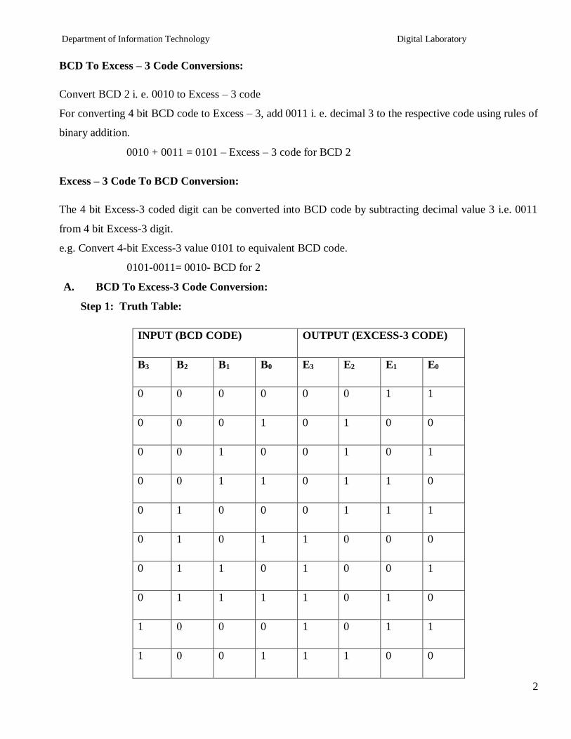
Department of Information Technology Digital Laboratory
2
BCD To Excess ndash 3 Code Conversions
Convert BCD 2 i e 0010 to Excess ndash 3 code
For converting 4 bit BCD code to Excess ndash 3 add 0011 i e decimal 3 to the respective code using rules of
binary addition
0010 + 0011 = 0101 ndash Excess ndash 3 code for BCD 2
Excess ndash 3 Code To BCD Conversion
The 4 bit Excess-3 coded digit can be converted into BCD code by subtracting decimal value 3 ie 0011
from 4 bit Excess-3 digit
eg Convert 4-bit Excess-3 value 0101 to equivalent BCD code
0101-0011= 0010- BCD for 2
A BCD To Excess-3 Code Conversion
Step 1 Truth Table
INPUT (BCD CODE) OUTPUT (EXCESS-3 CODE)
B3 B2 B1 B0 E3 E2 E1 E0
0 0 0 0 0 0 1 1
0 0 0 1 0 1 0 0
0 0 1 0 0 1 0 1
0 0 1 1 0 1 1 0
0 1 0 0 0 1 1 1
0 1 0 1 1 0 0 0
0 1 1 0 1 0 0 1
0 1 1 1 1 0 1 0
1 0 0 0 1 0 1 1
1 0 0 1 1 1 0 0
Department of Information Technology Digital Laboratory
3
Step 2 K-Map For Reduced Boolean Expressions Of Each Output
Fig 2 K-Map for Reduced Boolean Expressions Of Each Output (Excess-3 Code)
Department of Information Technology Digital Laboratory
4
Step3 Circuit Diagram Test the circuit for all possible combinations of input and output codes
4) Hardware Requirements Table
Table 1 Hardware Requirement Table
GATE Quantity
IC Quantity
XOR 1 7486 1
NOT 4 7404 1
AND 4 7408 1
OR 3 7432 1
Department of Information Technology Digital Laboratory
5
B Excess-3 To BCD Conversion
1 Truth Table
INPUT (EXCESS-3 CODE) OUTPUT (BCD CODE)
E3 E2 E1 E0 B3 B2 B1 B0
0 0 0 0 X X X X
0 0 0 1 X X X X
0 0 1 0 X X X X
0 0 1 1 0 0 0 0
0 1 0 0 0 0 0 1
0 1 0 1 0 0 1 01O6
51
0 1 1 0 0 0 1 1
0 1 1 1 0 1 0 0
1 0 0 0 0 1 0 1
1 0 0 1 0 1 1 0
1 0 1 0 0 1 1 1
1 0 1 1 1 0 0 0
1 1 0 0 1 0 0 1
1 1 0 1 X X X X
1 1 1 0 X X X X
1 1 1 1 X X X X
Department of Information Technology Digital Laboratory
6
2) K-Map For Reduced Boolean Expressions Of Each Output
Fig 5 K-Map For Reduced Boolean Expressions Of Each Output (BCD Code)
Department of Information Technology Digital Laboratory
7
3) Circuit Diagram Test the circuit for all possible combinations of input and output codes
4) Hardware Requirements Table
Table 2 Hardware Requirement Table
GATE Quantity
IC Quantity
XOR 1 7486 1
NOT 3 7404 1
AND 8 7408 2
OR 3 7432 1
Pin Diagrams
Department of Information Technology Digital Laboratory
8
7400 Quad 2-Input NAND Gate
7402 Quad 2-Input NOR Gate
7404 Not Gates
7408 Quad 2-Input AND Gates
7432 Quad 2-Input OR Gate
7486 Quad 2-Input Exclusive-OR Gate
Department of Information Technology Digital Laboratory
9
Conclusion
Thus we studied different codes and their conversions including applications
The truth tables have been verified using IC 7486 7432 7408 and 7404
FAQrsquos with answers
Q1) What is the need of code converters
There is a wide variety of binary codes used in digital systems Often it is required to convert from one
code to another For example the input to a digital system may be in natural BCD and output may be 7-
segment LEDs The digital system used may be capable of processing the data in straight binary format
Therefore the data has to be converted from one type of code to another type for different purpose
Q2) What is Gray code
It is a modified binary code in which a decimal number is represented in binary form in such a way that
each Gray- Code number differs from the preceding and the succeeding number by a single bit
(eg for decimal number 5 the equivalent Gray code is 0111 and for 6 it is 0101 These two codes differ
by only one bit position i e third from the left) It is non weighted code
Q3) What is the significance of Gray code
Important feature of Gray code is it exhibits only a single bit change from one code word to the next in
sequence Whereas by using binary code there is a possibility of change of all bits if we move from one
number to other in sequence (eg binary code for 7 is 0111 and for 8 it is 1000) Therefore it is more
useful to use Gray code in some applications than binary code
Q4) What are applications of Gray code
1 Important feature of Gray code is it exhibits only a single bit change from one code word to the next in
sequence This property is important in many applications such as Shaft encoders where error
susceptibility increases with number of bit changes between adjacent numbers in sequence
2 It is sometimes convenient to use the Gray code to represent the digital data converted from the analog
data (Outputs of ADC)
3 Gray codes are used in angle-measuring devices in preference to straight forward binary encoding
Department of Information Technology Digital Laboratory
10
4 Gray codes are widely used in K-map
Q5) What are weighted codes and non-weighted codes
In weighted codes each digit position of number represents a specific weight The codes 8421 2421 and
5211 are weighted codes Non weighted codes are not assigned with any weight to each digit position ie
each digit position within the number is not assigned a fixed value Gray code Excess-3 code are non-
weighted code
Q6) Why is Excess-3 code called as self-complementing code
Excess-3 code is called self-complementing code because 9rsquos complement of a coded number can be
obtained by just complementing each bit
Q7) What is invalid BCD
With four bits sixteen numbers (0000 to 1111) can be represented but in BCD code only 10 of these are
used as decimal numbers have only 10 digits fro 0 to 9 The six code combinations (1010 to 1111) are not
used and are invalid
Department of Information Technology Digital Laboratory
11
Regularity Content Viva-voce Timely
Submission Total
Dated Sign of
Subject
Teacher
2 4 2 2 10
Date of Performance Date of Completion
-------------------------------------------------------------------------------------------------------------------
Assignment No 2
------------------------------------------------------------------------------------------------------------------
Title BCD amp Excess 3 Adder
------------------------------------------------------------------------------------------------------------------
Objective 1 To study the BCD arithmetic rules
2 Comparison between binary and BCD codes
Problem Statement Design (truth table K-map) and implementation of 4-bit BCD to Excess-3 and
Excess-3 to BCD Code converters
-----------------------------------------------------------------------------------------------------------------
Hardware Requirement
i) IC 7483 (4 bit Binary adder) IC 7404(Hex INV) 7432 (OR-gate) 7408 (AND-gate)
ii) 7486 (EX-OR gate)
iii) Digital Trainer Kit -1
iv) Patch cords
----------------------------------------------------------------------------------------------------------------
Software Requirement Digital Work 30
------------------------------------------------------------------------------------------------------------------
Theory
BCD-Binary coded decimal-In this code each decimal digit represent by a 4-bit binary no BCD is a
way to express each of the decimal digits with binary code Positional weights associated to the binary bits
in BCD code are (MSB) 8-4-2-1(LSB)
BCD number 0 to 9 but greater than 9 is invalid BCD
Department of Information Technology Digital Laboratory
12
So Convert in valid BCD using add 6 ie (0110)
BCD Adder
BCD adder is a circuit that adds two BCD digits amp produces a sum of digits also in BCD
Rules for BCD addition
1 Add two numbers using rules of Binary addition
2 If the 4 bit sum is greater than 9 or if carry is generated then the sum is invalid To correct the sum
add 0110 i e (6)10 to sum If carry is generated from this addition add it to next higher order BCD
digit
3 If the 4 bit sum is less than 9 or equal to 9 then sum is in proper form
CASE I Sum lt= 9 amp carry = 0
Add BCD digits 3 amp 4
1 0 0 1 1
+ 0 1 0 0
------------
0 1 1 1
Answer is valid BCD number = (7)BCDamp so 0110 is not added
CASE II Sum gt 9 amp carry = 0
Add BCD digits 6 amp 5
1 0 1 1 0
+ 0 1 0 1
-----------
10 1 1
Department of Information Technology Digital Laboratory
13
Invalid BCD (since sum gt 9) so 0110 is to be added
2 1 0 1 1
+ 0 1 1 0
-----------
1 0 0 0 1
(1 1)BCD
Valid BCD result = (11) BCD
CASE III Sum lt = 9 amp carry = 1
Add BCD digits 9 amp 9
1 1 0 0 1
+1 0 0 1
-----------
1 0 0 1 0
Invalid BCD ( since Carry = 1 ) so 0110 is to be added
2 1 0 0 1 0
+ 0 1 1 0
------------
1 1 0 0 0
(1 8)BCD
Valid BCD result = (18) BCD
Design of BCD adder
1 To execute first step i e binary addition of two 4 bit numbers we will use IC 7483
( withCin = 0 ) which is 4 bit binary adder
2 We need to design a digital circuit which will sense sum amp carry of IC 7483 amp if sum exceeds 9 or
carry = 1 this digital circuit will produce high output otherwise its output will be zero
Circuit to check invalid BCD
Department of Information Technology Digital Laboratory
14
First we will design circuit to check sum amp then we will logically OR output of this circuit to carry
output of IC 7483
For digital circuit which we are going to design we will have 4 inputs
( S3 S2 S1 S0) amp only 1 output Y
a) Y output of this circuit Will be ORed with carry output of first adder IC
7483
b) If BCD result is invalid i e sum output of first 7483 we have to add
(6)10 ie (0110)2 that means we need one more binary adder IC 7483
c) If BCD result is valid ( ie final output of the circuit to check validity is 0) we will make an
arrangement that second adder IC 7483 adds (0)10 i e ( 0000 )2 to the sum of the first adder IC 7483
The output of the combinational circuit is used as final output carry amp carry output of second adder IC is
ignored
i ) Truth Table for design of combinational circuit for BCD adder to check invalid
BCD
K-map for output- Y=S3S2+S3S1
Department of Information Technology Digital Laboratory
15
iii) Circuit diagram
v) Hardware Requirements
GATE Quantity
IC Quantity
Binary adder 2 7483 2
AND 2 7408 1
OR 2 7432 1
B ) Design and Implement single digit EXCESS-3 adder using IC 7483
Excess-3 code is a non weighted code It is a modified form of a BCD code The Excess-3 code can be
derived from the natural BCD code by adding 3 to each coded number It is also known as Self
Complementary code
Excess-3 code is a self complementary code because 1rsquos complement of Excess-3 number is Excess-3
code for the 9rsquos complement of corresponding number
Output of BCD adder
Department of Information Technology Digital Laboratory
16
Eg Excess-3 code for (4)10 is (0111)XS-3 1rsquos complement of this number is 1000 which is Excess-3 code
for (5)10and 5 is 9rsquos complement of (4)10
Rules for Excess-3 addition
i Add two Exceess-3 numbers
ii If carry is 1 add 3 to Sum
iii If carry is 0 subtract 3 from sum
Eg (8)10 + (6)10
(8)10 = 1011 (Excess-3 for 8)
(6)10= 1001 (Excess-3 for 6)
_______________
1 0100
0011 0011
_______________
0100 0111 ( Excess 3 code for (14)10
(i)Design
1) 4 bit Binary addition of excess 3 codes of two operands can be implemented with IC 7483
2) We have to design the circuit which will either add 0011 or subtract 0011 ie add 1101 (2rsquos
complement of 0011)depending upon carry bit
Letrsquos compare 0011 and 1101
B3 B2 B1 B0
0 0 1 1 ------- When carry is 1
1 1 0 1 ------- When carry is 0
Here B0 bit in both situation is High
Now compare B3 B2 and B1 It is complement of each other
When carry is 1 Bit B1 =1 B2=B3=0
When carry is 0 Bit B1 =0 B2=B3=1
B1 bit follows the carry and B2 and B3 bit complements the carry
(ii) Circuit Diagram
Department of Information Technology Digital Laboratory
17
(iii ) HARDWARE REQUIREMENTS
Sl No IC Description Quantity
1 7404 Not Gate 01
2 7483 4 bit Binary Adder 04
CONCLUSION
BCD adder ampsubtractor is designed amp tested for all possible combinations
FAQrsquos
1 Explain and Write the significance of BCD number system
2 Write the applications of BCD amp Excess 3 code
3 Explain the rules of BCD amp Excess 3 arithmetic
4 What is the difference between BCD and binary codes
5 What do you mean by unpacked and packed BCD nos
Department of Information Technology Digital Laboratory
18
Regularity Content Viva-voce Timely
Submission Total
Dated Sign of
Subject
Teacher
2 4 2 2 10
+
Date of Performance Date of Completion
-------------------------------------------------------------------------------------------------------------------
Assignment No 3
---------------------------------------------------------------------------------------------------------------------------
Title Implementation of logic functions
----------------------------------------------------------------------------------------------------------------------
Objective 1 To study the difference between multiplexer demultiplexer and decoder
2To study the applications of multiplexer
---------------------------------------------------------------------------------------------------------------------
Problem Statement Implement of Logic function using multiplexer IC 74153
---------------------------------------------------------------------------------------------------------------------
Hardware Requirement
i) IC 74153 74138 7404 7432
ii) Digital Trainer Kit -1
iii) Patch cords
----------------------------------------------------------------------------------------------------------------
Software Requirement Digital Work 30
------------------------------------------------------------------------------------------------------------------
Theory
D CWigital Multiplexer
Multiplexer are combinational digital circuits equating as controlled switches with several data inputs (I0
I1 I2 hellip) amp one single data output (ldquooutrdquo)At any time one of the Ip is transmitted to output According to
binary signals applied on control pairs to circuit Usually the number of data inputs is a power of two
Multiplexing is the process of transmitting a large no of information units over a small no of channel
digital multiplexer is a combinational large circuit which performs the operation of multiplexing It selects
Department of Information Technology Digital Laboratory
19
the operation of multiplexing It selects the operation of binary information from one of the many input
lines amp transfer to a single op line Multiplexer is called a data selector or multiposition switch because it
selects one of the many input Selection of a particular line is controlled by a set of a selection lines or
selects inputs The number of select lines depends upon no of input lines Generally there
is lsquonrsquo selects line for lsquomrsquo input lines By applying a particular code on select lines is transmitted on the
output linesBlock diagram of MUX is shown at contains lsquo2mrsquo input lines lsquomrsquo select Such that 2m = n amp
one unable input which is used to activate or dedicate MUX Depending upon the no of IP amp OP lines
various types of multiplexers are available We have 21 41 81 161 MUX Here the first no indicates
the no of input lines amp second no indicates the no of output lines
E is called as enable input which is generally active low
Fig-Block diagram for N1 Multiplxer
Demultiplexer
Demultiplexer is a logic used to perform exactly reverse function performed by multiplexer It accepts a
single input and distributes among several outputs The selection of a particular output line is controlled
by a set of selection line There are n input lines amp 2m is the number of selection line whose bit
combinations determine which output to be selected
Encoder amp Decoder
1 Encoders are used to encode given digital number into different numbering format like
decimal to BCD Encoder Octal to Binary
2 Decoders are used to decode a coded binary word like BCD to seven segment decoder
3 Thus encoder and decoder are application specific logic develop we can not use any type of
input for any encoder and decoder
Smhelliphellips1 s0
Output(Y)
D0
D1
D2
D3
Dn
N1
multiplxer
E
Department of Information Technology Digital Laboratory
20
4 Need to select input according to encoder and decoder being selected for a particular
application as mention in examples above
Uses of Mux
1 Use for Boolean function implementation
2 Construct a common bus system
3 To select between multiple sources amp signal destination
4 Inter register transfer
Advantages
1) Simplification of logic expression not required
2) Logic design is simplified
Disadvantage
Only one function can be implemented using one MUX Hence they canrsquot be used in
combinational logic circuit which contains many function
Part-A (IC 74153)
1 VERIFICATION OF IC 74153
IC 74153 is a dual layer 41 MUX It has four input lines for (I0D-I3D) for second MUX amp active high
output lsquoYarsquo lsquoYbrsquo (1Y or 2Y) It has select lines S1S0 common to both MUX The Enable inputs are
active low EaampEb(1G and 2G) The MUX is activated when they are at logic o
Pin out of IC 74153
Department of Information Technology Digital Laboratory
21
Function table of IC 74153 (X= Donrsquot Care Condition)
Select Input
Inputs (I or II) Output
S1 S0 E (I or II) D0 D1 D2 D3 Y
X X 1 X X X X 0
0 0 0 0 X X X 0
0 0 0 1 X X X 1
0 1 0 X 0 X X 0
0 1 0 X 1 X X 1
1 0 0 X X 0 X 0
1 0 0 X X 1 X 1
1 1 0 X X X 0 0
1 1 0 X X X 1 1
2CASCADING OF IC 74153
Cascading is done to expand two or more MUX ICrsquos to a digital multiplexer with larger no of inputs ie
multiplexer stocks or tress is designed The enable input is used for cascading In case of IC 74153 we
have only two select lines But for certain application 3 select lines are required then it can be
obtained by cascading using enable Now with 3 select lines we have 8 combinations Out of this
combination the MSB is O MSB is 1 for last four combination so we can use these MSB to select
any 1 MUX out of two by connecting it to E pin of first 41 MUX
Function table of IC 74153 as 8 1 Mux by cascading 2 41 Mux
Select Input Output
C (1G 2G ) B (S1) A (S0) Y
0 0 0 D0
0 0 1 D1
0 1 0 D2
0 1 1 D3
1 0 0 D4
1 0 1 D5
Department of Information Technology Digital Laboratory
22
1 1 0 D6
1 1 1 D7
3FUNCTION IMPLEMENTATION
Y= sum m (1 3 5 6)
Thisexpression is in Standard SOP form and it is three variable function So we need to use mux with
three select inputs ie 81 Mux Already we have implemented 81 Mux using IC 74153 For Boolean
function in Standard SOP form we connect data inputs corresponding to the minterms present in the given
function to Vcc and remaining data inputs to ground
Truth table
Inputs Output
C B A Y
0 0 0 0
0 0 1 1
0 1 0 0
0 1 1 1
1 0 0 0
1 0 1 1
1 1 0 1
1 1 1 0
LOGIC DIAGRAM
Hardware Requirements
GATE Quantity
IC Quantity
Mux 1 74153 1
NOT 1 7404 1
OR 1 7432 1
Department of Information Technology Digital Laboratory
23
Part-B Decoder (IC 74138)
Theory
Discrete quantities of information are requested in digital system with binary codes A binary code of n
bits is capable of representing into 2n distinct elements of the coded information
Decoder converts coded input to coded outputs accepts one of the code
There are different types of decoders such as 38 decoder 416 line decoders etc These are in general
called as n m line decoder where m=2n and n= no of input lines and m=no of output lines Demux also
takes one input data line source and selectively distributes it to one of n output channels The only
difference between demux and decoder is that demux has Din (data ip) line whereas decoder does not
have
ADVANTAGES
1) The decoder provides best implementation whenever there are many outputs of the combinational
circuit and each op of the function (or its complement) is required to be expressed with a small no
of minterms
2) The decoder can function as demux If the Enable ip line is taken as Din (data ip)
DISADVANTAGES
Since decoder method requires an OR gate for each op function so there is new hardware used And it is
always advisable to use minimum hardware as we come across problems like propagation delay of gates
APPLICATIONS
Decoder is worthily used for decoding binary information and memory interfacing It is used for the
implementation of Boolean function
Differentiate between Mux Demux Decoder
Point Multiplexer Demultiplexer Decoder
Input Many input lines Single input line Many input line also Acts as select line
Output Single output line Many output line Many output lineActive low output
Select line 2m = n n = 2m Enable inputs used
Department of Information Technology Digital Laboratory
24
A) Verification of IC 74138
We use IC 74138 which accepts 3 binary weighted inputs (A0 A1 A2) and when enabled provides
mutually exclusive active low outputs (y0-y7) It features 3 Enable ips Two active low (G2A G2B) and
one active high (G1) Every output will be high unless G2A G2Bare low and G1 is high It has
demultiplexing capability and multiple enable ips for easy expansion
IC Diagram
Function Table of 38 decoder
Input Output
Enable Data
G2A G2B G1 A2 A1 A0 Y0 Y1 Y2 Y3 Y4 Y5 Y6 Y7
0 0 0 X X X 1 1 1 1 1 1 1 1
0 1 1 X X X 1 1 1 1 1 1 1 1
1 0 1 X X X 1 1 1 1 1 1 1 1
1 1 1 X X X 1 1 1 1 1 1 1 1
Department of Information Technology Digital Laboratory
25
0 0 1 0 0 0 0 1 1 1 1 1 1 1
0 0 1 0 0 1 1 0 1 1 1 1 1 1
0 0 1 0 1 0 1 1 0 1 1 1 1 1
0 0 1 0 1 1 1 1 1 0 1 1 1 1
0 0 1 1 0 0 1 1 1 1 0 1 1 1
0 0 1 1 0 1 1 1 1 1 1 0 1 1
0 0 1 1 1 0 1 1 1 1 1 1 0 1
0 0 1 1 1 1 1 1 1 1 1 1 1 0
B) Cascading of IC 74138
The enable ip G1 active high of IC 74138 is used for cascadingfor cascading 2 ICrsquos the enable ip G1 of
first IC is connected to G1 enable ip of second IC through a NOT gate This enable ip is used as MSB
select ip line A3 the other three select input lines of both ICrsquos (A0A1A2) are also shorted to select
input lines of second IC to get single ip select lines (A0A1A2)
The ip line A3 is used to enable disable the 2 IC 74138 decoders When A3=0 first IC is enabled and
second is disabled Thus the first decoder will generate minterms from 0000 to 0111 as op and the second
decoder will generate nothing When A3=1 the enable conditions are reversed and thus second decoder
IC will generate minterms 1000 to 1111
Function Table of 416 decoder using IC 74138 (38 decoder)
Input Output
Enable Data
G2
A
G2
B
A
3
A
2
A
1
A
0
Y
0
Y
1
Y
2
Y
3
Y
4
Y
5
Y
6
Y
7
Y
8
Y
9
Y1
0
Y1
1
Y1
2
Y1
3
Y1
4
Y1
5
0 1 X X X X 1 1 1 1 1 1 1 1 1 1 1 1 1 1 1 1
Department of Information Technology Digital Laboratory
26
1 0 X X X X 1 1 1 1 1 1 1 1 1 1 1 1 1 1 1 1
1 1 X X X X 1 1 1 1 1 1 1 1 1 1 1 1 1 1 1 1
0 0 0 0 0 0 0 1 1 1 1 1 1 1 1 1 1 1 1 1 1 1
0 0 0 0 0 1 1 0 1 1 1 1 1 1 1 1 1 1 1 1 1 1
0 0 0 0 1 0 1 1 0 1 1 1 1 1 1 1 1 1 1 1 1 1
0 0 0 0 1 1 1 1 1 0 1 1 1 1 1 1 1 1 1 1 1 1
0 0 0 1 0 0 1 1 1 1 0 1 1 1 1 1 1 1 1 1 1 1
0 0 0 1 0 1 1 1 1 1 1 0 1 1 1 1 1 1 1 1 1 1
0 0 0 1 1 0 1 1 1 1 1 1 0 1 1 1 1 1 1 1 1 1
0 0 0 1 1 1 1 1 1 1 1 1 1 0 1 1 1 1 1 1 1 1
0 0 1 0 0 0 1 1 1 1 1 1 1 1 0 1 1 1 1 1 1 1
0 0 1 0 0 1 1 1 1 1 1 1 1 1 1 0 1 1 1 1 1 1
0 0 1 0 1 0 1 1 1 1 1 1 1 1 1 1 0 1 1 1 1 1
0 0 1 0 1 1 1 1 1 1 1 1 1 1 1 1 1 0 1 1 1 1
0 0 1 1 0 0 1 1 1 1 1 1 1 1 1 1 1 1 0 1 1 1
0 0 1 1 0 1 1 1 1 1 1 1 1 1 1 1 1 1 1 0 1 1
0 0 1 1 1 0 1 1 1 1 1 1 1 1 1 1 1 1 1 1 0 1
0 0 1 1 1 1 1 1 1 1 1 1 1 1 1 1 1 1 1 1 1 0
C) Implementation of Boolean function
The procedure for implementation of combinational circuit by means of a decoder and lsquoORrsquo gates requires
that the Boolean function fir the circuit be expressed in Sum of Minterms These forms can be obtained by
Department of Information Technology Digital Laboratory
27
expanding the function A decoder is then chosen which generates all the minterms of n ip variables The
ip to each OR gate are selected from the decoder outputs according to the minterms list in each function
i) F1=summ (1 3 5 7)
Truth table
Logic Diagram
ii) F2=summ (1 3 5 7111315)
Truth table
Logic Diagram
Conclusion In this way multiplexer Decoderamp its applications are studied implemented amp
tested
FAQrsquos
1What is a multiplexer
2What is a Demultiplexer
3 Enlist applications of multiplexer
Department of Information Technology Digital Laboratory
28
Regularity Content Viva-voce Timely
Submission Total
Dated Sign of
Subject
Teacher
2 4 2 2 10
Date of Performance Date of Completion
-------------------------------------------------------------------------------------------------------------------
Assignment No4
------------------------------------------------------------------------------------------------------------------
Title 3 bit updown Asynchronous and Synchronous counter using IC7476
------------------------------------------------------------------------------------------------------------------
Objective To understand design procedure of asynchronousamp Synchronous counter
------------------------------------------------------------------------------------------------------------------
Problem Statement Design (State diagram state table amp K map) and implementation of 3
bit Up and Down Asynchronous and Synchronous Counter using master slave JK flip-flop IC 7476
-----------------------------------------------------------------------------------------------------------------
Hardware Requirement
i) IC 7476 (MS-JK Flip-flop) IC 7408(Quad 2 ip AND Gate)
IC 7432 (Quad 2 ip OR Gate) and IC 7404 (Hex Inverter)
ii) Digital Trainer Kit -132
iii) Patch cords
----------------------------------------------------------------------------------------------------------------
Software Requirement Digital Work 30
------------------------------------------------------------------------------------------------------------------
Theory
Counters counters are logical device or registers capable of counting the no of states or no of clock
pulses arriving at its clock input where clock is a timing parameter arriving at regular intervals of time
so counters can be also used to measure time amp frequencies They are made up of flip flops Where the
Department of Information Technology Digital Laboratory
29
pulse are counted to be made of it goes up step by step amp the op of counter in the flip flop is decoded to
read the count to its starting step after counting n pulse incase of module counters
Types of Counters
Counter are of two types
1) Asynchronous counter
2) Synchronous counter
Asynchronous counter
A digital counter is a set of flip flop The flip flop are connected such that their combined state at any time
is binary equivalent of total no of pulses that have occurred up to that time Thus its name implies a
counter is used to count pulse A counter is used as frequency dividers To obtain waveform with
frequency that is specific fraction of clock frequency
Counter may be Asynchronous or synchronous The Asynchronous counter is also called as ripple counter
An Asynchronous counter uses T flip flop to perform a counting function The actual hardware used is
usually J-K flip flop with J amp K connected to logic1Even D flip flops may be used here
In asynchronous counter commonly called ripple counter the first flip-flop is clocked by the external
clock pulse amp then each successive flip-flop is clocked by the Q or Qrsquo output of the previous flip-flop
Therefore in an asynchronous counter the flip-floprsquos are not clocked simultaneously The input of MS-JK
is connected to VCC because when both inputs are one output is toggled As MS-JK is negative edge
triggered at each high to low transition the next flip-flop is triggered
Synchronous Counter
When counter is clocked such that each flip flop in the counter is
triggered at the same time the counter is called as synchronous counter
The gates propagation delay at reset time will not be present or we may say will not occur
1) Asynchronous Up Counter
Fig 1 shows 3bit Asynchronous Up Counter Here Flip-flop 2 act as a MSB Flip-flop and Flip-flop 0 act
as a LSB Flip-flop Clock pulse is connected to the Clock of Flip-flop 0 Output of Flip-flop 0(Q0) is
connected to clock of next flip-flop (ie Flip-flop 1) and so on As soon as clock pulse changes output is
going to change (at the negative edge of clock pulse) as a Up count sequence For 3 bit Up counter state
table is as shown below
Department of Information Technology Digital Laboratory
30
State Table
Logic diagram
Fig 1 3 Bit Asynchronous Up Counter
Hardware requirements
Gate
Flip flop
Quantity IC Quantity
MS JK 3 7476 2
2) Down Counter
Fig 2 shows 2 bit Asynchronous Down Counter Here Flip-flop 2 act as a MSB Flip-flop and Flip-flop 0
act as a LSB Flip-flop Clock pulse is connected to the Clock of Flip-flop 0 Output of Flip-flop 0 (Q0rsquo) is
Counter States Count
Q2 Q1 Q0
0 0 0 0
1 0 0 1
2 0 1 0
3 0 1 1
4 1 0 0
5 1 0 1
6 1 1 0
7 1 1 1
8 0 0 0
Department of Information Technology Digital Laboratory
31
connected to clock of next flip-flop (ie Flip-flop 1) and so on As soon as clock pulse changes output is
going to change (at the negative edge of clock pulse) as a down count sequence For 3 bit down counter
sate table is as shown below
In both the counters Inputs J and K are connected to Vcc hence J-K Flip flop work in toggle mode Preset
and Clear both are connected to logic 1
State Table
Logic diagram
Fig 2 3 Bit Asynchronous Down Counter
Hardware requirements
Counter States Count
Q2 Q1 Q0
7 1 1 1
6 1 1 0
5 1 0 1
4 1 0 0
3 0 1 1
2 0 1 0
1 0 0 1
0 0 0 0
7 1 1 1
Department of Information Technology Digital Laboratory
32
Gate
Flip flop
Quantity IC Quantity
MS JK 3 7476 2
Applications
The asynchronous counters are specially used as the counting devices
They are also used to count number of pulses applied
It also works as frequency divider
It helps in counting the number of product coming out of the machinery where product is coming out at
equal interval of time
Types of synchronous counter
1) Up counter
2) Down counter
1 3 bit Synchronous up counter
The up counter counts from 0 to7 ie(000 to 111)for this we are using MS JK flip flop In IC 74LS76 2
MS J-K flip flops are present The clock pulse is given at pin 1 amp 6 of the 1st IC amp pin 1 of 2nd IC Next
state decoder logic is designed with the help of state table
State table for synchronous up counter
Present state Next state Flip flop 3 Flip flop 2 flip flop 1
Q2 Q1 Q0 Q2 Q2 Q0 J2 K2 J1 K1 J0 K0
0 0 0 0 0 1 0 x 0 X 1 x
0 0 1 0 1 0 0 x 1 X x 1
0 1 0 0 1 1 0 x x 0 1 x
0 1 1 1 0 0 1 x x 1 x 1
1 0 0 1 0 1 x 0 0 X 1 X
1 0 1 1 1 0 x 0 1 X x 1
1 1 0 1 1 1 x 0 x 0 1 X
1 1 1 0 0 0 x 1 x 1 x 1
Department of Information Technology Digital Laboratory
33
K-Map
Q1Q0
Q2
00 01 11 10
0 0 0 1 0
1 X X X X
J2= Q1Q0
Q1Q0
Q2
00 01 11 10
0 X X X X
1 0 0 1 0
K2= Q1Q0
Q1Q0
Q2
00 01 11 10
0 0 1 X X
1 0 1 X X
J1= Q0
Q1Q0
Q2
00 01 11 10
0 X X 1 0
1 X X 1 0
K1= Q0
Department of Information Technology Digital Laboratory
34
Q1Q0
Q2
00 01 11 10
0 1 X X 1
1 1 X X 1
J0= 1
Q1Q0
Q2
00 01 11 10
0 X 1 1 X
1 X 1 1 X
K0= 1
Logic Diagram
Fig 1 3 bit Synchronous up counter
Department of Information Technology Digital Laboratory
35
2 3 bit Synchronous down counter
This is used to count from 7-0 ie(111-000)for this also 2 ICrsquos of 74LS76 are required amp hence we use 3
MS JK flip flops Here also clock is given to 1stamp 6th pin of 1st IC amp1st pin of 2nd IC enabling to apply
clock to all flip flop at a time Next state decoder logic is designed with the help of state table
State table for synchronous down counter
Present state Next state Flip flop 3 Flip flop 2 Flip flop 1
Q2 Q1 Q0 Q2 Q1 Q0 J2 K2 J1 K1 J0 K0
1 1 1 1 1 0 X 0 X 0 X 1
1 1 0 1 0 1 X 0 X 1 1 X
1 0 1 1 0 0 X 0 0 X X 1
1 0 0 0 1 1 X 1 1 X 1 X
0 1 1 0 1 0 0 X X 0 X 1
0 1 0 0 0 1 0 X X 1 1 X
0 0 1 0 0 0 0 X 0 X X 1
0 0 0 1 1 1 1 X 1 X 1 X
K-Map
Q1Q0
Q2
00 01 11 10
0 1 0 0 0
1 X X X X
J2= Q1Q0
Q1Q0
Q2
00 01 11 10
Department of Information Technology Digital Laboratory
36
0 X X X X
1 1 0 0 0
K2= Q1Q0
Q1Q0
Q2
00 01 11 10
0 1 0 X X
1 1 0 X X
J1= Q0
Q1Q0
Q2
00 01 11 10
0 X X 0 1
1 X X 0 1
K1= Q0
Q1Q0
Q2
00 01 11 10
0 1 X X 1
1 1 X X 1
J0= 1
Q1Q0
Q2
00 01 11 10
0 X 1 1 X
1 X 1 1 X
K0= 1
Department of Information Technology Digital Laboratory
37
Logic Diagram
Fig 2 3 bit Synchronous down counter
Uses
1 Specially used as the counting devices
2 Used in frequency divider circuit
3 Used in digital voltmeter
4 Used in counter type A to D converter
5 Used for time measurement
6 It helps in counting the no of product coming out from machinery where product is coming out
at equal interval of time
Conclusion
Up and down counters are successfully implemented the counters are studied amp op are checked The
state table is verified
PRACTICE ASSIGNMENTS EXERCISE MODIFICATIONS
1 Design amp implement 2 bit controlled synchronous counter
2 Designamp implement 4 bit controlled synchronous counter
3 Designamp implement truncated synchronous up or down counter
FAQrsquos with answers
1 What do you mean by Counter
A Counter is a register capable of counting the no of clock pulses arriving at its
clock inputs Count represents the no of clock pulses arrived A specified
sequence of states appears as the counter output
Department of Information Technology Digital Laboratory
38
2 What are the types of Counters Explain each
There are two types of counters as Asynchronous Counter and Synchronous Counter
Asynchronous Counter In this counter the first flip-flop is clocked by the external clock pulse
and then each successive flip-flop is clocked by the Q or Qrsquo op of the previous flip-flop Hence in
Asynchronous Counter flip-flops are not clocked simultaneously and hence called as Ripple
Counter Synchronous Counter In this counter the common clock input is connected to all the
flip-flops simultaneously
3 What do you mean by pre-settable counters
A counter in which starting state is not zero can be designed by making use of the
preset inputs of the flip flops This is referred to as loading the counter
asynchronously This is referred to as pre-settable counter
4 What are the applications of synchronous counters
Digital clock
Frequency divider circuits
Frequency counters
Used in analog to digital converters
5 What are the advantages of synchronous counters over asynchronous counters
Propagation delay time is reduced
Can operate at a much higher frequency than the asynchronous counters
6 Ring counter is an example of synchronous counters or asynchronous counter
Synchronous counter Since all the flip flops are clocked simultaneously
7 Twisted Ring (Johnsonrsquos) counter is an example of synchronous counters or asynchronous
counter
Synchronous counter Since all the flip flops are clocked simultaneously
8 What is the difference between ring counter and twisted ring counter
In ring counter pulses to be counted are applied to a counter it goes from state to state and the
output of the flip flop s in the counter is decoded to read the count Here the uncomplimentary
output (Q) of last flip flop is fed back as an input to first flip flop Ring counters are referred as
MOD lsquoNrsquo counters
Department of Information Technology Digital Laboratory
39
But in Twisted ring counter the complimentary output (Q bar) of last flip flop is fed back as an
input to first flip flop Twisted Ring counters are referred as MOD lsquo2Nrsquo counters
9 What are the applications of ring counters
Ring counter outputs are sequential non-overlapping pulses which are useful for control state
counters Used in stepper motor this requires pulses to rotate it from one position to the next Used
as divide by lsquoNrsquo ((MOD lsquoNrsquo) counters
10 What are the applications of ring counter twisted ring counters
Used as divide by lsquo2Nrsquo ((MOD lsquo2Nrsquo) counters
Used for control state counters
Used for generation of multiphase clock
11 List the Synchronous Counter ICs
IC 74160 Decade Up Counter
IC 74161 4 bit binary Up Counter
IC 74162 Decade Up Counter
IC 74163 4 bit binary Up Counter
IC 74168 Decade UpDown Counter
IC 74169 4 bit Binary UpDown Counter
IC 74190 Decade UpDown Counter
IC 74191 4 bit Binary UpDown Counter
IC 74192 Decade UpDown Counter
IC 74193 4 bit Binary UpDown Counter
Department of Information Technology Digital Laboratory
40
Regularity Content Viva-voce Timely
Submission Total
Dated Sign of
Subject
Teacher
2 4 2 2 10
Date of Performance Date of Completion
-------------------------------------------------------------------------------------------------------------------
Assignment No 5
-------------------------------------------------------------------------------------------------------------------------------
Title Design and implementation of Module lsquonrsquo counter with IC7490 and IC 74191
-----------------------------------------------------------------------------------------------------------------------------
Objective To know difference between regular amp truncated counter as well as binary ampBCD Counter
--------------------------------------------------------------------------------------------------------------------------------
Problem Statement To design and implement mod - 10 mod ndash 7 mod - 99 asynchronous BCD
counter using IC 7490 and to design and implement up down mod - n Binary counter using IC 74191
-----------------------------------------------------------------------------------------------------------------
Hardware Requirement
i) IC 7490 IC 74191 basic gates
ii) Digital Trainer Kit -1
iii) Patch cords
----------------------------------------------------------------------------------------------------------------
Software Requirement Digital Work 30
------------------------------------------------------------------------------------------------------------------
Theory
Part A ndash IC 7490
IC 7490 is a TTL MSI (medium scale integration) decade counter It contains 4 master slave flip flops
internally connected to provide MOD-2 ie divide by 2 and MOD-5 ie divide by 5 counters MOD-2 and
Mod-5 counters can be used independently or in cascading
Department of Information Technology Digital Laboratory
41
It is a 4-bit ripple type decade counter The device consists of 4-master slave flip flops internally
connected to provide a divide by two and divide by 5 sections Each section has a separate clock ip to
initiate state changes of the counter on the high to low clock transition
Since the op from the divide by 2 section is not internally connected to the succeeding stages The device
may be operated in various counting modes In a BCD counter the CP1 input must be externally connected
to QA op The CP0ip receives the incoming count producing a BCD count sequence It is also provided
with additional gating to provide a divide by 2 counter and binary counter for which the count cycle length
is divide by 5 The device may be operated in various counting modes
There are 2 reset inputs R0(1) and R0(2) both of which need to be connected to the lsquologic 1rsquo for clearing all
flip flops Two set inputs Rg(1) and Rg(2) when connected to logic 1 are used for setting counter to 1001
(BCD 9)
Pin out of IC 7490
Fig Pin configuration of IC7490
Table 1-pin name and description of IC7490
Pin name Description
Input B This is clock input to the internal MOD-5 ripple counter which is negative
edge triggered
R0(1)R0(2) Gated zero reset inputs
Department of Information Technology Digital Laboratory
42
R9(1)R9(2) These are gated set to nine inputs
QDQCQB Output of internal MOD-5 counter with QD as MSB
QA Output of internal MOD-2 counter with QA as LSB
Input A Clock input to FF-A which is negative edge triggered
Functional Table for IC7490
Reset inputs Output
R0(1) R0(2) R9(0) R9(1) QD QC QB QA
1 1 0 X 0 0 0 0
1 1 X 0 0 0 0 0
X X 1 1 1 0 0 1
X 0 X 0 COUNTER
0 X 0 X COUNTER
0 X X 0 COUNTER
X 0 0 x COUNTER
Department of Information Technology Digital Laboratory
43
Basic internal Structure of IC 7490
Function Table of MOD-5 counter
Design of MOD-10 counter using IC 7490
The QA op the first flip flop is connected to the input B which is clock ip of internal MOD-5 ripple
counter Due to cascading of Mod-2 and Mod-5 counters the overall configuration the decade counters
count from 0000 to 1001 After 1001 mod-5 resets to 0000 and next count after 1001 is 0000
When QA op is connected to B ip we have the Mod-2 counter followed by Mod-5 counter The
count sequence obtained is shown in the table It may be noted that QA changes from 0 to 1 the state of
InputB clock Output
Count QD QC QB
0 0 0 0
0 0 1 1
0 1 0 2
0 1 1 3
1 0 0 4
Department of Information Technology Digital Laboratory
44
Mod-5 counter doesnrsquot change whereas when QA changes from 1 to 0 the Mod-5 counter goes to the next
state
Logic DiagramMOD-10 counter using IC 7490
5 Modulus n Counter
Function table
Ip clock
Output
Count QD QC QB QA
0 0 0 0 0
0 0 0 1 1
0 0 1 0 2
0 0 1 1 3
0 1 0 0 4
Department of Information Technology Digital Laboratory
45
Design of Mod-7 Counter using IC 7490
Mod-7 counter counts through seven states from 0 to 6 counters and it should reset as soon as the
count becomes 7 The op of reset logic should be 1 corresponding to invalid states The reset logic op
should be applied to pin 2 and 3
Truth Table of Reset Logic
0 1 0 1 5
0 1 1 0 6
0 1 1 1 7
1 0 0 0 8
1 0 0 1 9
QD QC QB QA Y
0 0 0 0 0
0 0 0 1 0
0 0 1 0 0
0 0 1 1 0
0 1 0 0 0
0 1 0 1 0
0 1 1 0 0
0 1 1 1 1
1 0 0 0 1
1 0 0 1 1
Department of Information Technology Digital Laboratory
46
Logic Diagram Mod 7 Counter using IC 7490
Function table
Ip clock
Output
Count QD QC QB QA
0 0 0 0 0
0 0 0 1 1
0 0 1 0 2
0 0 1 1 3
0 1 0 0 4
0 1 0 1 5
0 1 1 0 6
Department of Information Technology Digital Laboratory
47
Design of Mod-99 using IC 7490
For Mod-99 two IC 7490rsquos will be required Hence to implement a divide by 99 counter we have
to use two decade counters ICrsquos A divide by 99 counter counts 99 states from 0 to 98 and the counter
should reset as soon as the count becomes 99 So in order to reset the counter of 99 connect the Q op
which are equal to 1 in the count of 99 to an lsquoAndrsquo gate amp then connect and op to the reset ip of both
ICrsquos
MOD-100 Counter-
MOD-100 counter can be obtained by cascading two decade counter ICrsquos
Each IC gives divide by 10 counts Hence 2 ICs will give 1010=100 counts
Clock is applied to the input A of IC 7490 the Q1 output is connected to B input etc
For cascading the QD output of the first IC is connected to the input A of second IC Thus QD of
IC-(1) acts as clock input to IC-(2)
The Ro (1) Ro(2) R9(1) R9(2) inputs of both ICs are connected to ground so as to make them
inactive
The total count provided by the two counters varies from 00 to 99 decimal that means 100 states
Hence it is a MOD-10 counter
Impleacutementations
FigureMOD-100 counters using IC 7490
Department of Information Technology Digital Laboratory
48
B) IC 74191 ndash Theory
IC74191 is 4-bit binary synchronous reversible up down counter It contains 4 master slave flip flops
with internal gating and steering logic to provide asynchronous reset and synchronous count updown
operations its asynchronous parallel capability permits the counter to be preset to any desire number D0
to D3 are the parallel data inputs Information present on the parallel data inputs D0 to D3 is loaded into
the counter and appears on the output when the load PLinput is lowThisoperation overrides the counting
function Counting is inhabited by the high level on the enable G input when G input is low internal state
changes are initiated synchronously by the low to high transitions of the clock inputs the updown input
signal determines the direction of input
Function Table
Operating
mode
Inputs Outputs
PL UD G CLK Dn
Parallel
load L X X X L L
L X X X H H
Count up H L 0 uarr X Count up
Count
down H H 0 uarr X
Count
down
Hold(No
change) H X H X X No change
Pin details ndash
D0 to D3 input lines PL parallel load
G is Enable input ndash enabling the counting
Q0 to Q3 output lines
Downup determines the direction of counting
Clk clock input for counter
Terminal Count Max(1111) min(0000) For these states signal goes high for 1clock pulse
Ripple clock Clock input for next higher state
Department of Information Technology Digital Laboratory
49
Pin Diagram IC 74191
Up counter- Truth Table
Clk
Pulses QA QB QC QD
0 0 0 0 0
1 0 0 0 1
2 0 0 1 0
3 0 0 1 1
4 0 1 0 0
5 0 1 0 1
6 0 1 1 0
7 1 1 1 1
8 1 0 0 0
9 1 0 0 1
10 1 0 1 0
11 1 0 1 1
12 1 1 0 0
13 1 1 0 1
Department of Information Technology Digital Laboratory
50
14 1 1 1 0
15 1 1 1 1
Logic Diagram
Steps-
Connect the circuit as shown above
Apply clock ip to pin no14
Connect UD to GND
Verify the output according to truth table
Logic diagram of down counter
Steps-
Connect the circuit as shown above
Apply clock ip to pin no14
Connect UD to VCC
Verify the output according to truth table
UD D3 D2 D1 D0 PL
Clock IC 74191
G RC
MAX MIN
Q3 Q2 Q1 Q0 TC
vcc
NC
NC
Outputs
no connection
vcc
Department of Information Technology Digital Laboratory
51
With the help of IC74191 we can implement truncated updown counter by using following logic ndash
Connect data input line to particular count you want to load
According to requirement make Truth table
Draw the K-map
Find out Boolean expression
Draw the logic diagram and that is the combinational logic for your count and apply the output of
that circuit to PL
According to requirement we get the UP and down counting
5 Modulus n Counter
Presettable updown counter
Mod 11 counter
Implementation of presetttable mod updown counter using IC- 74LS191
1 Load Data on data lines D0 to D3 (0101)
2 Counter will go through the states from 0101 0110hellip1111 in up counter and 0101 to 0000 in
down counter
Combinational Circuit
CLOCK D3 D2 D1 D0
TC
U D 74191 RC
G PL
Updown Q3 Q2 Q1 Q0 PL
Q3 Q2 Q1 Q0
Preset Count
Department of Information Technology Digital Laboratory
52
3 The logic circuit should be designed in such a way that only when all the outputs are high output
of the reset circuit should be low and the counter should jump to state 5 It should again start
counting from 0101 to 0000
State Table
Down Counter UP Counter
IC 74191 is 4 bit counter Thus it counts 0000 to 1111 different 16 states For MOD11 counter we require
different 11 states so 5 steps must be skipped from 16 states We get MOD11 by presetting counter to
value 5
Assignment Question
Design and Implement MOD 7 MOD 10 and MOD 12 using IC 74191
FAQs
1 What do you mean modulus counter
Counter
state Clock
pulse
Q3 Q2 Q1 Q0
1 0 1 0 1
2 0 1 1 0
3 0 1 1 1
4 1 0 0 0
5 1 0 0 1
6 1 0 1 0
7 1 0 1 1
8 1 1 0 0
9 1 1 0 1
10 1 1 1 1
11 1 1 1 1
Counter state
Clock pulse
FF outputs
Q3 Q2 Q1 Q0
1 0 1 0 1
2 0 1 0 0
3 0 0 1 1
4 0 0 1 0
5 0 0 0 1
6 0 0 0 0
7 0 1 0 1
Department of Information Technology Digital Laboratory
53
It represents the number of possible states of counter
2 How will you use the 7490 IC to design symmetrical divide by 10 frequency counter
The divide by 5 circuit followed by divide by 2 circuit will give symmetrical output
3Where counters are used Give real life example of counter
Modulus n Counter
Binary counter ndash An N stage counter that recycles after 2 Ncount The count proceds in specified binary
sequence Counter Presetable- A counter which can be set to a desired value before the start of the
counting UPDown counter ndash A counter that can count in both up and down direction depending upon a
control input
Department of Information Technology Digital Laboratory
54
Regularity Content Viva-voce Timely
Submission Total
Dated Sign of
Subject
Teacher
2 4 2 2 10
Date of Performance Date of Completion
-------------------------------------------------------------------------------------------------------------------
Assignment No6
------------------------------------------------------------------------------------------------------------------
Title Sequence Generator
------------------------------------------------------------------------------------------------------------------
Objective To understand sequence generator one of the sequential circuit
-------------------------------------------------------------------------------------------------------------------
Problem Statement Design (State Diagram State Table K Map) and implementation of Sequence
Generator using Shift Register IC 74194
-----------------------------------------------------------------------------------------------------------------
Hardware Requirement
i) IC 741947408 (AND-gate) 7432 (OR-gate)
ii) Digital Trainer Kit -1
iii) Patch cords
----------------------------------------------------------------------------------------------------------------
Software Requirement Digital Work 30
------------------------------------------------------------------------------------------------------------------
Theory
Part A Sequence Generator with Flip flop
A sequential circuit which generates a prescribed sequence of bits in synchronism with a clock is referred
to as a sequence generator These pulse trains or sequence of bits can be used to open valves close gates
turn on lights and turn off machines and other variety of jobs
Department of Information Technology Digital Laboratory
55
For the design of sequence generator we first determine the required no of flip flops and the logic circuit
for the next state decoder
No of flip flops required to generate particular sequence can be determined as follows
1) Find the no of 1rsquos in the sequence
2) Find the no of 0rsquos in the sequence
3) Take the maximum out of two
4) If N is the required no of flip flops choose minimum value of lsquonrsquo to satisfy equation given below
Max (0rsquos 1rsquos) le 2n-1
The sequence generator can be classified as
1) sequence generator without bushing
2) sequence generator with bushing
The aim in this experiment is to design a sequence generator to generate a sequence of bit ie 10101
Part B Sequence Generator using Shift Register IC 74194
IC 74194 4 bit bidirectional Shift Register
This bidirectional shift register is designed to incorporate virtually all the features a system designer may
want in a shift register they feature Parallel inputs parallel outputs right shift left shift serialinputs
operating mode control inputsand a direct overriding clear line The register has four distinct modes of
operationsnamely
1 Parallel load
2 Shift right (in the direction QA towards QD)
3 Shift left (in the direction QD towards QA)
4 Inhibit clock (do nothing)
Synchronous parallel loading is accomplished by applying the four bits of data and taking both
mode control inputs S0 and S1High The data is loaded in to the associated flip-flops and appear
at the outputs after positive transition of the clock input During loading serial data flow is
inhibited
Shift right is accomplished synchronously with the rising edge of the clock pulse when S0 is High
and S1 is Low Serial data for this mode is entered at the shift right data input When S0 is Low
and S1 is High data shifts left synchronously and new data is entered at the shift left serial input
Clocking of the flip flop is inhibited when both mode control inputs are LOW
Department of Information Technology Digital Laboratory
56
Mode Control Input Operation
S1 S0
0 0 Clock Inhibit
0 1 Shift right
1 0 Shift Left
1 1 Parallel loading
Function Table of IC 74194
Design
The minimum number of flip-flops N required to generate a sequence of length S is given by S
le 2N ndash 1
In this case S=7 therefore the minimum value of N which may generate in this sequence is 3
However it is not guaranteed to lead to a solution If the given sequence leads to seven distinct
states then only three flip flops are sufficient otherwise we have to increase the number of flip
flops We write the states of circuit as given in table 1 The prescribed sequence is listed under QA
and the sequence listed under QB and QC are the same sequence delayed by one and two clock
pulses respectively From the table we observe that all the states are not distinct which means N=3
is not sufficient Next we assume that N=4 and prepare table 2 The last column gives the required
serial input for getting the desired change of state when a clock pulse is applied This is obtained
by assuming D type flip flop and looking at the QA output For example at the falling edge of first
clock pulse QA=1 The second clock pulse must result in QA=1 which requires its D input to be 1
In the same manner all the entries in column Y are determined
Table 1 State Assignment Table of Sequence Generator (N=3)
Number of Clock
Pulses
Flip Flop Inputs States
QA QB QC
1 1 1 1 7
2 1 1 1 7
3 0 1 1 3
4 1 0 1 5
Department of Information Technology Digital Laboratory
57
5 0 1 0 2
6 1 0 1 5
7 1 1 0 6
Excitation table of D Flip-Flop
Present State Qn Next State Qn+1 Flip-Flop Input D
0 0 0
0 1 1
1 0 0
1 1 1
Table 2State Assignment Table of Sequence Generator (N=4)
Number of Clock
Pulses
Flip Flop Inputs States
Y
Serial ip QA QB QC QD
1 1 1 1 0 14 1
2 1 1 1 1 15 0
3 0 1 1 1 7 1
4 1 0 1 1 11 0
5 0 1 0 1 5 1
6 1 0 1 0 10 1
7 1 1 0 1 13 1
K-Map Simplification
Department of Information Technology Digital Laboratory
58
00 01 11 10
00 X X X X
01 X 1 1 X
11 X 1 0 1
10 X X 0 1
Y= QArsquo + QBrsquo + QCrsquo = QAQBQC
LOGIC DIAGRAM
HARDWARE REQUIREMENTS
Sr no ICs Description Quantity
11 74194 4 bit bidirectional universal shift register 16ktr`
2 7410 3 input NAND Gate 1
Department of Information Technology Digital Laboratory
59
Conclusion In this way sequence generator using JK flip flips amp shift register is designed and
implemented
Enhancements Modifications ndash Sequence generator can also be implemented with shift register instead
of flip flops Use IC 7495 universal shift register IC and try to implement sequence generator
FAQs
1 What is sequential logic circuit
A sequential logic circuit consists of a memory elements in addition to
combinational circuit Its output at any instant of time depends upon
the present input as well as present state of memory element
2 What is meant by delay line
It is used to introduce time delays in digital signals
3 What is meant by following terms
a) Synchronous preset b) Asynchronous preset
c) Synchronous clear d) Asynchronous clear
a)Preset operation is synchronised with the clock
b)Preset operation is independent of the clock
c) clear is performed in synchronous with clock
d) clear is performed independent with clock
4 Is asynchronous counter faster than synchronous counter
In a synchronous counter the time required for change of any state is same and is equal to delay
time of one flip flop where as in asynchronous counter all flip flops are not clocked
simultaneously hence time required is not same
5 What is mean by lockout in counter
In a counter design for a fewer state than the maximum possible state some time it may so happen
that counter enters in unused state and goes from one unused state to another unused state and
never comes to used state
6 What is mean by state table
Department of Information Technology Digital Laboratory
60
It consists of complete information about present state and next state and outputs of a sequential
system
7 What is mean by state diagram
The information available in a state table can be represented as graphically the graphical
representation is known as state diagram
8 What is the advantage of state reduction in the design of sequential circuit
It reduces the number of flip flops
9 What is meant by excitation table
This gives information about what should be the flip flop inputs if outputs are specified before and
after the clock pulse
10 How many flip flops are required to design sequence generator using Counters
max (0rsquoS1rsquoS) in a given sequence lt= 2(N - 1)
Where N = Number of flip flops
11 How many flip flops are required to design sequence generator using shift registers
Slt= 2N - 1
Where N=Number of flip flops
S= Length of sequence
12 What is Lock out condition How it is avoided
When counter enters into one of the invalid state and after application of pulses remains in invalid
states only i e counter gets locked into invalid state amp this is called as lock out Lock out can be
avoided by providing bushing to all the invalid states in such a way that after application of one or
more clock pulses counter will fall into one of the valid state
Department of Information Technology Digital Laboratory
61
Regularity Content Viva-voce Timely
Submission Total
Dated Sign of
Subject
Teacher
2 4 2 2 10
Date of Performance Date of Completion
-------------------------------------------------------------------------------------------------------------------
Assignment No7
------------------------------------------------------------------------------------------------------------------
Title Multiplexer using Data flow modeling and structural modeling
------------------------------------------------------------------------------------------------------------------
Objective To learn data flow modeling style Its uses and different types of declarations with some
different types of circuits Structure of VHDL program is well discussed with this modeling style
-------------------------------------------------------------------------------------------------------------------
Problem Statement 41 multiplexer using data flow amp structural modeling -
----------------------------------------------------------------------------------------------------------------
Hardware Requirement - NA
----------------------------------------------------------------------------------------------------------------
Software Requirement Xilinx
------------------------------------------------------------------------------------------------------------------
Theory
Data flow style-
In this type of design the view of data as flowing from input to output through a design
An operation is defined in terms of a collection of data transformation expressed as concurrent
statement Each of the statement can be activated when any of its input signal changes its value While
these statements describe the behavior of the circuit a lot of information about its structure can be
extracted from the description as well
Data flow modeling has a set of concurrent assignment statements In the data flow level of abstraction we
describe how information is passed in the circuit The built in operators in VHDL are used in expression
such as AND OR XOR NOT etc
Department of Information Technology Digital Laboratory
62
INPUT
Two select lines S1S0
Four data lines D0 D1 D2 D3
OUTPUT
One output line Y
Functional block diagram of 41 Mux
Fig 41 Multiplexer using Data flow modeling
Function table of 41 Mux
Enable S1 S0 A B C D Y
1 X X X X X X 0
0 0 0 A X X X A
0 0 1 X B X X B
0 1 0 X X C X C
0 1 1 X X X D D
Design steps
Click on Xilinx ISE 92i
Create New project from file menu Ensure top level source is HDL
Select family of devices (usually spartan2E or 3)
Department of Information Technology Digital Laboratory
63
Ensure preferred language is VHDL
Click new source which shows you project details device details
and Synthesis and simulator tools
After finishing project create new source by right clicking in project name with VHDL
module
Complete ports name directions and bus Ensure architecture name is behavioral
After that we will get design summary and detailed reports
Close design summary
Create your code with given modeling style
Go to process window and synthesis to check if any error is there in code Check syntax and
view RTL schematic
Create new source to simulate the code
Right click on source name and create test bench waveform with proper name Ensure the
project is same
Click on combinational circuit in initial timing wizard
Select test bench wave in source window Apply inputs to wave diagram Ensure you are in
behavioral simulation
Go to process box Click on Xilinx ISE simulator and simulate the model See results
RTL Schematic
Department of Information Technology Digital Laboratory
64
Timing Diagram
FAQrsquos
1 What are the different kinds of data objects in VHDL code
Ans data object may be any value or number still some signal data objects and bit and bit_vector
types of these are available in VHDL STD_LOGIC and STD_LOGIC_VECTOR types are used
widely in programming
2 What do you mean by signal
Ans signal is a data object represents logic signals or wires in a circuit There are three places in
which signals can be declared in VHDL code in an entity declaration in the declarative section of
architecture and in declarative section of package
3 What are different signal types
Ans BIT BIT_VECTOR STD_LOGIC STD_LOGIC_VECTOR STD_ULOGIC SIGNED
UNSIGNED INTEGER ENUMERATION and BOOLEAN
4 What is an entity
Ans a circuit or sub circuit described with VHDL code is called a design entity
5 Explain structure of an entity
Ans it has two main parts the entity declaration which specifies the input and output signals for
entity and the architecture which gives circuit details
Department of Information Technology Digital Laboratory
65
6 How will you declare a package with component Explain structure
The general form of package declaration is as shown in diagram
PACKAGE package_name IS
[TYPE declarations]
[SIGNAL declarations]
[COMPONENT declarations]
END package_name
Entity
Declaration Architecture
Department of Information Technology Digital Laboratory
66
Regularity Content Viva-voce Timely
Submission Total
Dated Sign of
Subject
Teacher
2 4 2 2 10
Date of Performance Date of Completion
-------------------------------------------------------------------------------------------------------------------
Assignment No8
------------------------------------------------------------------------------------------------------------------
Title Full Adder using Behavioral and Structural modeling
------------------------------------------------------------------------------------------------------------------
Objective To learn structural modeling style Its uses and different types of declarations with some
different types of circuits Structure of VHDL program is well discussed with this modeling style
-------------------------------------------------------------------------------------------------------------------
Problem Statement Full adder using behavioral amp structural modeling
-----------------------------------------------------------------------------------------------------------------
Hardware Requirement - NA
----------------------------------------------------------------------------------------------------------------
Software Requirement Xilinx
------------------------------------------------------------------------------------------------------------------
Theory
Structural style-
A digital electronic system can be described as a module with inputs andor outputs The electrical values
on the outputs are same functions of the values of inputs The example of it is as shown The NAND gate
has 2ips AampB amp an output y Using VHDL terminology we call the NAND2 design entity amp the inputs
amp outputs are called ports 1 way of describing the function of NAND2 is to describe how it is composed
of sub modules AND amp INVERTER Each of the Sub modules is an instance of some entity amp ports of the
instances are connected using signals Structural modeling has a set of interconnected component
Structure can be used to create a very low level description of a circuit or a very high level description
Department of Information Technology Digital Laboratory
67
In a gate level description of a circuit for example components such as basic logic gates amp FFs might be
connected in some logical stricture to create the circuit This is what is often called a net list
Structure of structural modeling
Functional block diagram of Full Adder
architectureNetlistofHalf_Adderis
-- component with locals
componentMyXorport (A_XorB_Xor in BIT
Z_Xor out BIT)
end component
-- component with locals
componentMyAndport (A_AndB_And in BIT
Z_And out BIT)
end component
begin
Xor1 MyXorport map (X Y Sum)
-- instance with actuals
And1 MyAndport map (X Y Cout)
-- instance with actuals
end
Department of Information Technology Digital Laboratory
68
Function table of Full Adder
A B Cin SUM CARRY
0 0 0 0 0
0 0 1 1 0
0 1 0 1 0
0 1 1 0 1
1 0 0 1 0
1 0 1 0 1
1 1 0 0 1
1 1 1 1 1
Sum = Σm(1 2 4 7)
Carry= Σm(3 5 6 7)
Design steps
Click on Xilinx ISE 92i
Create New project from file menu Ensure top level source is HDL
Select family of devices (usually spartan2E or 3)
Ensure preferred language is VHDL
Click new source which shows you project details device details
and Synthesis and simulator tools
After finishing project create new source(full adder) by right clicking in project name with
VHDL module
Complete ports name directions and bus Ensure architecture name is behavioral
After that we will get design summary and detailed reports
Close design summary
Click new source which shows you project details device details
and Synthesis and simulator tools
After finishing project create new source(half adder) by right clicking in project name with
VHDL module
Complete ports name directions and bus Ensure architecture name is behavioral Names
should be same as previous inputs
Department of Information Technology Digital Laboratory
69
After that we will get design summary and detailed reports
Close design summary
Create your code for half adder with given modeling style
After that go to process window Click on design utilities
View HDL instantiation code of half adder
Copy component part of half adder in architecture block of full adder Copy instantiation
template twice after begin as we require two half adders to construct full adder (structural
modeling) Name them differently (eg ha1 or ha2)
Create signals as per the logic Complete code of full adder
Go to process window and synthesis to check if any error is there in code Check syntax and
view RTL schematic
Create new source to simulate the code
Right click on source name and create test bench waveform with proper name Ensure the
project is same
Click on combinational circuit in initial timing wizard
Select test bench wave in source window Apply inputs to wave diagram Ensure you are in
behavioral simulation
Go to process box Click on Xilinx ISE simulator and simulate the model See results
RTL Schematic
Timing Diagram
Department of Information Technology Digital Laboratory
70
INPUT
Three inputs A B Carry (previous)
OUTPUT
Two outputs Sum Carry
FAQrsquos
1 What do you mean by structural style
Ans in this type of code a circuit is described in hierarchical fashion by connecting together sub
circuits
2 Explain IF statement with example
Ans The general form of an IF statement is as follws
IF Sel=rsquo0rsquo THEN
Flt=x1
ELSE
Flt=x2
END IF
Department of Information Technology Digital Laboratory
71
3 Explain declaration and instantiation process in VHDL
Ans first declare a small vhdl code in formal way Eg half adder Define project name is full adder
And simply copy instantiation template in main source code Define how many times you want to
declare this template Give separate names for those
4 What is STD_LOGIC_VECTOR
Ans It is standard data object added to VHDL standard in IEEE 1164 It provides more flexibility
than the Bit type
5 Explain difference between concurrent and sequential statements
Ans Concurrent statements define interconnected processes and blocks that together describe a designrsquos
overall behavior or structure They can be grouped using block sstatement Groups of blocks can also be
partitioned into other blocks At this same level a VHDL component can be connected to define signals
within the blocks
It is a reference to an entity A process can be a single signal assignment statement or a series of
sequential statements (SS) Within a process procedures and functions can partition the sequential
statements
PRACTICE ASSIGNMENTS
1 Implement half adder using data flow modeling
2 Implement Full Adder using behavioral modeling
3 Implement 3 bit magnitude comparator using a 3 bit adder
4 Implement half sub tractor using data flow modeling
5 Write VHDL code for Full Subtractor
Department of Information Technology Digital Laboratory
72
Regularity Content Viva-voce Timely
Submission Total
Dated Sign of
Subject
Teacher
2 4 2 2 10
rsquozaDate of Performance Date of Completion
-------------------------------------------------------------------------------------------------------------------
Assignment No9
------------------------------------------------------------------------------------------------------------------
Title Simulation of 3 bit Connter using Behavioral modeling
------------------------------------------------------------------------------------------------------------------
Objective To learn behavioral modeling style Its uses and different types of declarations with some
different types of circuits Structure of VHDL program is well discussed with this modeling style
-------------------------------------------------------------------------------------------------------------------
Problem Statement 3 bit controlled up down synchronous counter with preset amp clear
-----------------------------------------------------------------------------------------------------------------
Hardware Requirement -NA
----------------------------------------------------------------------------------------------------------------
Software Requirement Xilinx
------------------------------------------------------------------------------------------------------------------
Theory
Behavioral style-
Highest level of abstraction supported in VHDL is called the behavior level of abstraction In it we have
for loop while loop If then else case ampvariable assignment The statements are enclosed in a PROCESS
block amp are executed sequentially
In it circuit is described in terms of its operation overtime
In behavioral description the concept of time may be expressed precisely with actual delays between
related events (such as the propagation delays within gates amp on wires) or it may be simply an ordering of
operation that are expressed sequentially (such as in a functional description of a FF)
Department of Information Technology Digital Laboratory
73
A behavioral design method defines a circuit in terms of text language rather than a schematic of
interconnected symbols
Behavioral design is a technology independent text based design that incorporates high level
functionality amp high level information flow
Structure of Behavioral modeling
Functional block diagram of 3 bit controlled up down synchronous counter with preset amp clear
Function table of 3 bit controlled up down synchronous counter with preset amp clear
Design steps
Click on Xilinx ISE 92i
Create New project from file menu Ensure top level source is HDL
Select family of devices (usually spartan2E or 3)
Ensure preferred language is VHDL
Click new source which shows you project details device details
and Synthesis and simulator tools
After finishing project create new source by right clicking in project name with VHDL
module
Complete ports name directions and bus Ensure architecture name is behavioral
After that we will get design summary and detailed reports
Close design summary
Create your code with given modeling style
Go to process window and synthesis to check if any error is there in code Check syntax
and view RTL schematic Create new source to simulate the code
Department of Information Technology Digital Laboratory
74
Right click on source name and create test bench waveform with proper name Ensure the
project is same
Click on combinational circuit in initial timing wizard
Select test bench wave in source window Apply inputs to wave diagram Ensure you are in
behavioral simulation
Go to process box Click on Xilinx ISE simulator and simulate the model
RTL Schematic
Timing Diagram
INPUT
Clock Preset Clear
OUTPUT
Three output lines
FAQrsquos
1 Explain the structure of behavioral modeling
2 What are the differences between behavioral and structural modeling
Ans Behavioral descriptionof a circuit is the highest level of abstraction in VHDL Here the
circuit is described in terms of it operation with respect to time All operations are in one level of
code The operations are described in a way that the designer of a sequential circuit infers a
register
Structural description on the other hand is a circuit description in terms of its components
it can either create a low level description much like a hierarchy in a block diagram Whenever
you see a component instantiated in a code that code employs structural description of the circuit
The components are connected in the form of a netlist This is for better manageability and
reusability
3 What are the differences between behavioral and data flow modeling
Department of Information Technology Digital Laboratory
75
Ans Behavioral ndash describes how the output is derived from the inputs using structured
statements
Dataflow ndash describes how the data flows from the inputs to the output most often
using NOT AND and OR operations
4 What do you mean by process statement
Ans The process statement begins with the PROCESS keyword followed by a parenthesized list
of signals called the sensitivity list It operates on selected and conditional statements
5 Explain syntax of process statement
Ans BEGIN
Process( sensitivity list)
END process
PRACTICE ASSIGNMENTS
1 Implement 3 bit asynchronous up counter using behavioral modeling
2 Implement 3 bit asynchronous down counter using behavioral modeling
3 Implement 3 bit synchronous down counter using behavioral modeling
End
Department of Information Technology Digital Laboratory
76
Pin Diagrams
7400 Quad 2-Input NAND Gate
7402 Quad 2-Input NOR Gate
7404 Not Gates
7408 Quad 2-Input AND Gates
7432 Quad 2-Input OR Gate
7486 Quad 2-Input Exclusive-OR Gate
Department of Information Technology Digital Laboratory
77
7483 4 bit Binary Adder
7490 Decade and Binary Counters
74138 38 Decoder
Department of Information Technology Digital Laboratory
78
74153 Dual 41 Multiplexer
74191 Synchronous UpDown 4 bit Binary counter with Mode Control
Department of Information Technology Digital Laboratory
79
74194 Universal Shift Register
7476 Dual Master-Slave J-K Flip-Flops
- Part B Sequence Generator using Shift Register IC 74194
-
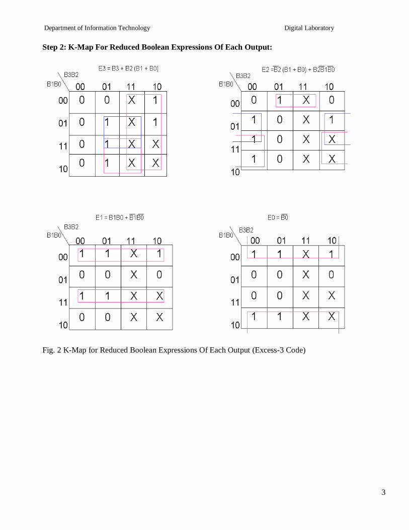
Department of Information Technology Digital Laboratory
3
Step 2 K-Map For Reduced Boolean Expressions Of Each Output
Fig 2 K-Map for Reduced Boolean Expressions Of Each Output (Excess-3 Code)
Department of Information Technology Digital Laboratory
4
Step3 Circuit Diagram Test the circuit for all possible combinations of input and output codes
4) Hardware Requirements Table
Table 1 Hardware Requirement Table
GATE Quantity
IC Quantity
XOR 1 7486 1
NOT 4 7404 1
AND 4 7408 1
OR 3 7432 1
Department of Information Technology Digital Laboratory
5
B Excess-3 To BCD Conversion
1 Truth Table
INPUT (EXCESS-3 CODE) OUTPUT (BCD CODE)
E3 E2 E1 E0 B3 B2 B1 B0
0 0 0 0 X X X X
0 0 0 1 X X X X
0 0 1 0 X X X X
0 0 1 1 0 0 0 0
0 1 0 0 0 0 0 1
0 1 0 1 0 0 1 01O6
51
0 1 1 0 0 0 1 1
0 1 1 1 0 1 0 0
1 0 0 0 0 1 0 1
1 0 0 1 0 1 1 0
1 0 1 0 0 1 1 1
1 0 1 1 1 0 0 0
1 1 0 0 1 0 0 1
1 1 0 1 X X X X
1 1 1 0 X X X X
1 1 1 1 X X X X
Department of Information Technology Digital Laboratory
6
2) K-Map For Reduced Boolean Expressions Of Each Output
Fig 5 K-Map For Reduced Boolean Expressions Of Each Output (BCD Code)
Department of Information Technology Digital Laboratory
7
3) Circuit Diagram Test the circuit for all possible combinations of input and output codes
4) Hardware Requirements Table
Table 2 Hardware Requirement Table
GATE Quantity
IC Quantity
XOR 1 7486 1
NOT 3 7404 1
AND 8 7408 2
OR 3 7432 1
Pin Diagrams
Department of Information Technology Digital Laboratory
8
7400 Quad 2-Input NAND Gate
7402 Quad 2-Input NOR Gate
7404 Not Gates
7408 Quad 2-Input AND Gates
7432 Quad 2-Input OR Gate
7486 Quad 2-Input Exclusive-OR Gate
Department of Information Technology Digital Laboratory
9
Conclusion
Thus we studied different codes and their conversions including applications
The truth tables have been verified using IC 7486 7432 7408 and 7404
FAQrsquos with answers
Q1) What is the need of code converters
There is a wide variety of binary codes used in digital systems Often it is required to convert from one
code to another For example the input to a digital system may be in natural BCD and output may be 7-
segment LEDs The digital system used may be capable of processing the data in straight binary format
Therefore the data has to be converted from one type of code to another type for different purpose
Q2) What is Gray code
It is a modified binary code in which a decimal number is represented in binary form in such a way that
each Gray- Code number differs from the preceding and the succeeding number by a single bit
(eg for decimal number 5 the equivalent Gray code is 0111 and for 6 it is 0101 These two codes differ
by only one bit position i e third from the left) It is non weighted code
Q3) What is the significance of Gray code
Important feature of Gray code is it exhibits only a single bit change from one code word to the next in
sequence Whereas by using binary code there is a possibility of change of all bits if we move from one
number to other in sequence (eg binary code for 7 is 0111 and for 8 it is 1000) Therefore it is more
useful to use Gray code in some applications than binary code
Q4) What are applications of Gray code
1 Important feature of Gray code is it exhibits only a single bit change from one code word to the next in
sequence This property is important in many applications such as Shaft encoders where error
susceptibility increases with number of bit changes between adjacent numbers in sequence
2 It is sometimes convenient to use the Gray code to represent the digital data converted from the analog
data (Outputs of ADC)
3 Gray codes are used in angle-measuring devices in preference to straight forward binary encoding
Department of Information Technology Digital Laboratory
10
4 Gray codes are widely used in K-map
Q5) What are weighted codes and non-weighted codes
In weighted codes each digit position of number represents a specific weight The codes 8421 2421 and
5211 are weighted codes Non weighted codes are not assigned with any weight to each digit position ie
each digit position within the number is not assigned a fixed value Gray code Excess-3 code are non-
weighted code
Q6) Why is Excess-3 code called as self-complementing code
Excess-3 code is called self-complementing code because 9rsquos complement of a coded number can be
obtained by just complementing each bit
Q7) What is invalid BCD
With four bits sixteen numbers (0000 to 1111) can be represented but in BCD code only 10 of these are
used as decimal numbers have only 10 digits fro 0 to 9 The six code combinations (1010 to 1111) are not
used and are invalid
Department of Information Technology Digital Laboratory
11
Regularity Content Viva-voce Timely
Submission Total
Dated Sign of
Subject
Teacher
2 4 2 2 10
Date of Performance Date of Completion
-------------------------------------------------------------------------------------------------------------------
Assignment No 2
------------------------------------------------------------------------------------------------------------------
Title BCD amp Excess 3 Adder
------------------------------------------------------------------------------------------------------------------
Objective 1 To study the BCD arithmetic rules
2 Comparison between binary and BCD codes
Problem Statement Design (truth table K-map) and implementation of 4-bit BCD to Excess-3 and
Excess-3 to BCD Code converters
-----------------------------------------------------------------------------------------------------------------
Hardware Requirement
i) IC 7483 (4 bit Binary adder) IC 7404(Hex INV) 7432 (OR-gate) 7408 (AND-gate)
ii) 7486 (EX-OR gate)
iii) Digital Trainer Kit -1
iv) Patch cords
----------------------------------------------------------------------------------------------------------------
Software Requirement Digital Work 30
------------------------------------------------------------------------------------------------------------------
Theory
BCD-Binary coded decimal-In this code each decimal digit represent by a 4-bit binary no BCD is a
way to express each of the decimal digits with binary code Positional weights associated to the binary bits
in BCD code are (MSB) 8-4-2-1(LSB)
BCD number 0 to 9 but greater than 9 is invalid BCD
Department of Information Technology Digital Laboratory
12
So Convert in valid BCD using add 6 ie (0110)
BCD Adder
BCD adder is a circuit that adds two BCD digits amp produces a sum of digits also in BCD
Rules for BCD addition
1 Add two numbers using rules of Binary addition
2 If the 4 bit sum is greater than 9 or if carry is generated then the sum is invalid To correct the sum
add 0110 i e (6)10 to sum If carry is generated from this addition add it to next higher order BCD
digit
3 If the 4 bit sum is less than 9 or equal to 9 then sum is in proper form
CASE I Sum lt= 9 amp carry = 0
Add BCD digits 3 amp 4
1 0 0 1 1
+ 0 1 0 0
------------
0 1 1 1
Answer is valid BCD number = (7)BCDamp so 0110 is not added
CASE II Sum gt 9 amp carry = 0
Add BCD digits 6 amp 5
1 0 1 1 0
+ 0 1 0 1
-----------
10 1 1
Department of Information Technology Digital Laboratory
13
Invalid BCD (since sum gt 9) so 0110 is to be added
2 1 0 1 1
+ 0 1 1 0
-----------
1 0 0 0 1
(1 1)BCD
Valid BCD result = (11) BCD
CASE III Sum lt = 9 amp carry = 1
Add BCD digits 9 amp 9
1 1 0 0 1
+1 0 0 1
-----------
1 0 0 1 0
Invalid BCD ( since Carry = 1 ) so 0110 is to be added
2 1 0 0 1 0
+ 0 1 1 0
------------
1 1 0 0 0
(1 8)BCD
Valid BCD result = (18) BCD
Design of BCD adder
1 To execute first step i e binary addition of two 4 bit numbers we will use IC 7483
( withCin = 0 ) which is 4 bit binary adder
2 We need to design a digital circuit which will sense sum amp carry of IC 7483 amp if sum exceeds 9 or
carry = 1 this digital circuit will produce high output otherwise its output will be zero
Circuit to check invalid BCD
Department of Information Technology Digital Laboratory
14
First we will design circuit to check sum amp then we will logically OR output of this circuit to carry
output of IC 7483
For digital circuit which we are going to design we will have 4 inputs
( S3 S2 S1 S0) amp only 1 output Y
a) Y output of this circuit Will be ORed with carry output of first adder IC
7483
b) If BCD result is invalid i e sum output of first 7483 we have to add
(6)10 ie (0110)2 that means we need one more binary adder IC 7483
c) If BCD result is valid ( ie final output of the circuit to check validity is 0) we will make an
arrangement that second adder IC 7483 adds (0)10 i e ( 0000 )2 to the sum of the first adder IC 7483
The output of the combinational circuit is used as final output carry amp carry output of second adder IC is
ignored
i ) Truth Table for design of combinational circuit for BCD adder to check invalid
BCD
K-map for output- Y=S3S2+S3S1
Department of Information Technology Digital Laboratory
15
iii) Circuit diagram
v) Hardware Requirements
GATE Quantity
IC Quantity
Binary adder 2 7483 2
AND 2 7408 1
OR 2 7432 1
B ) Design and Implement single digit EXCESS-3 adder using IC 7483
Excess-3 code is a non weighted code It is a modified form of a BCD code The Excess-3 code can be
derived from the natural BCD code by adding 3 to each coded number It is also known as Self
Complementary code
Excess-3 code is a self complementary code because 1rsquos complement of Excess-3 number is Excess-3
code for the 9rsquos complement of corresponding number
Output of BCD adder
Department of Information Technology Digital Laboratory
16
Eg Excess-3 code for (4)10 is (0111)XS-3 1rsquos complement of this number is 1000 which is Excess-3 code
for (5)10and 5 is 9rsquos complement of (4)10
Rules for Excess-3 addition
i Add two Exceess-3 numbers
ii If carry is 1 add 3 to Sum
iii If carry is 0 subtract 3 from sum
Eg (8)10 + (6)10
(8)10 = 1011 (Excess-3 for 8)
(6)10= 1001 (Excess-3 for 6)
_______________
1 0100
0011 0011
_______________
0100 0111 ( Excess 3 code for (14)10
(i)Design
1) 4 bit Binary addition of excess 3 codes of two operands can be implemented with IC 7483
2) We have to design the circuit which will either add 0011 or subtract 0011 ie add 1101 (2rsquos
complement of 0011)depending upon carry bit
Letrsquos compare 0011 and 1101
B3 B2 B1 B0
0 0 1 1 ------- When carry is 1
1 1 0 1 ------- When carry is 0
Here B0 bit in both situation is High
Now compare B3 B2 and B1 It is complement of each other
When carry is 1 Bit B1 =1 B2=B3=0
When carry is 0 Bit B1 =0 B2=B3=1
B1 bit follows the carry and B2 and B3 bit complements the carry
(ii) Circuit Diagram
Department of Information Technology Digital Laboratory
17
(iii ) HARDWARE REQUIREMENTS
Sl No IC Description Quantity
1 7404 Not Gate 01
2 7483 4 bit Binary Adder 04
CONCLUSION
BCD adder ampsubtractor is designed amp tested for all possible combinations
FAQrsquos
1 Explain and Write the significance of BCD number system
2 Write the applications of BCD amp Excess 3 code
3 Explain the rules of BCD amp Excess 3 arithmetic
4 What is the difference between BCD and binary codes
5 What do you mean by unpacked and packed BCD nos
Department of Information Technology Digital Laboratory
18
Regularity Content Viva-voce Timely
Submission Total
Dated Sign of
Subject
Teacher
2 4 2 2 10
+
Date of Performance Date of Completion
-------------------------------------------------------------------------------------------------------------------
Assignment No 3
---------------------------------------------------------------------------------------------------------------------------
Title Implementation of logic functions
----------------------------------------------------------------------------------------------------------------------
Objective 1 To study the difference between multiplexer demultiplexer and decoder
2To study the applications of multiplexer
---------------------------------------------------------------------------------------------------------------------
Problem Statement Implement of Logic function using multiplexer IC 74153
---------------------------------------------------------------------------------------------------------------------
Hardware Requirement
i) IC 74153 74138 7404 7432
ii) Digital Trainer Kit -1
iii) Patch cords
----------------------------------------------------------------------------------------------------------------
Software Requirement Digital Work 30
------------------------------------------------------------------------------------------------------------------
Theory
D CWigital Multiplexer
Multiplexer are combinational digital circuits equating as controlled switches with several data inputs (I0
I1 I2 hellip) amp one single data output (ldquooutrdquo)At any time one of the Ip is transmitted to output According to
binary signals applied on control pairs to circuit Usually the number of data inputs is a power of two
Multiplexing is the process of transmitting a large no of information units over a small no of channel
digital multiplexer is a combinational large circuit which performs the operation of multiplexing It selects
Department of Information Technology Digital Laboratory
19
the operation of multiplexing It selects the operation of binary information from one of the many input
lines amp transfer to a single op line Multiplexer is called a data selector or multiposition switch because it
selects one of the many input Selection of a particular line is controlled by a set of a selection lines or
selects inputs The number of select lines depends upon no of input lines Generally there
is lsquonrsquo selects line for lsquomrsquo input lines By applying a particular code on select lines is transmitted on the
output linesBlock diagram of MUX is shown at contains lsquo2mrsquo input lines lsquomrsquo select Such that 2m = n amp
one unable input which is used to activate or dedicate MUX Depending upon the no of IP amp OP lines
various types of multiplexers are available We have 21 41 81 161 MUX Here the first no indicates
the no of input lines amp second no indicates the no of output lines
E is called as enable input which is generally active low
Fig-Block diagram for N1 Multiplxer
Demultiplexer
Demultiplexer is a logic used to perform exactly reverse function performed by multiplexer It accepts a
single input and distributes among several outputs The selection of a particular output line is controlled
by a set of selection line There are n input lines amp 2m is the number of selection line whose bit
combinations determine which output to be selected
Encoder amp Decoder
1 Encoders are used to encode given digital number into different numbering format like
decimal to BCD Encoder Octal to Binary
2 Decoders are used to decode a coded binary word like BCD to seven segment decoder
3 Thus encoder and decoder are application specific logic develop we can not use any type of
input for any encoder and decoder
Smhelliphellips1 s0
Output(Y)
D0
D1
D2
D3
Dn
N1
multiplxer
E
Department of Information Technology Digital Laboratory
20
4 Need to select input according to encoder and decoder being selected for a particular
application as mention in examples above
Uses of Mux
1 Use for Boolean function implementation
2 Construct a common bus system
3 To select between multiple sources amp signal destination
4 Inter register transfer
Advantages
1) Simplification of logic expression not required
2) Logic design is simplified
Disadvantage
Only one function can be implemented using one MUX Hence they canrsquot be used in
combinational logic circuit which contains many function
Part-A (IC 74153)
1 VERIFICATION OF IC 74153
IC 74153 is a dual layer 41 MUX It has four input lines for (I0D-I3D) for second MUX amp active high
output lsquoYarsquo lsquoYbrsquo (1Y or 2Y) It has select lines S1S0 common to both MUX The Enable inputs are
active low EaampEb(1G and 2G) The MUX is activated when they are at logic o
Pin out of IC 74153
Department of Information Technology Digital Laboratory
21
Function table of IC 74153 (X= Donrsquot Care Condition)
Select Input
Inputs (I or II) Output
S1 S0 E (I or II) D0 D1 D2 D3 Y
X X 1 X X X X 0
0 0 0 0 X X X 0
0 0 0 1 X X X 1
0 1 0 X 0 X X 0
0 1 0 X 1 X X 1
1 0 0 X X 0 X 0
1 0 0 X X 1 X 1
1 1 0 X X X 0 0
1 1 0 X X X 1 1
2CASCADING OF IC 74153
Cascading is done to expand two or more MUX ICrsquos to a digital multiplexer with larger no of inputs ie
multiplexer stocks or tress is designed The enable input is used for cascading In case of IC 74153 we
have only two select lines But for certain application 3 select lines are required then it can be
obtained by cascading using enable Now with 3 select lines we have 8 combinations Out of this
combination the MSB is O MSB is 1 for last four combination so we can use these MSB to select
any 1 MUX out of two by connecting it to E pin of first 41 MUX
Function table of IC 74153 as 8 1 Mux by cascading 2 41 Mux
Select Input Output
C (1G 2G ) B (S1) A (S0) Y
0 0 0 D0
0 0 1 D1
0 1 0 D2
0 1 1 D3
1 0 0 D4
1 0 1 D5
Department of Information Technology Digital Laboratory
22
1 1 0 D6
1 1 1 D7
3FUNCTION IMPLEMENTATION
Y= sum m (1 3 5 6)
Thisexpression is in Standard SOP form and it is three variable function So we need to use mux with
three select inputs ie 81 Mux Already we have implemented 81 Mux using IC 74153 For Boolean
function in Standard SOP form we connect data inputs corresponding to the minterms present in the given
function to Vcc and remaining data inputs to ground
Truth table
Inputs Output
C B A Y
0 0 0 0
0 0 1 1
0 1 0 0
0 1 1 1
1 0 0 0
1 0 1 1
1 1 0 1
1 1 1 0
LOGIC DIAGRAM
Hardware Requirements
GATE Quantity
IC Quantity
Mux 1 74153 1
NOT 1 7404 1
OR 1 7432 1
Department of Information Technology Digital Laboratory
23
Part-B Decoder (IC 74138)
Theory
Discrete quantities of information are requested in digital system with binary codes A binary code of n
bits is capable of representing into 2n distinct elements of the coded information
Decoder converts coded input to coded outputs accepts one of the code
There are different types of decoders such as 38 decoder 416 line decoders etc These are in general
called as n m line decoder where m=2n and n= no of input lines and m=no of output lines Demux also
takes one input data line source and selectively distributes it to one of n output channels The only
difference between demux and decoder is that demux has Din (data ip) line whereas decoder does not
have
ADVANTAGES
1) The decoder provides best implementation whenever there are many outputs of the combinational
circuit and each op of the function (or its complement) is required to be expressed with a small no
of minterms
2) The decoder can function as demux If the Enable ip line is taken as Din (data ip)
DISADVANTAGES
Since decoder method requires an OR gate for each op function so there is new hardware used And it is
always advisable to use minimum hardware as we come across problems like propagation delay of gates
APPLICATIONS
Decoder is worthily used for decoding binary information and memory interfacing It is used for the
implementation of Boolean function
Differentiate between Mux Demux Decoder
Point Multiplexer Demultiplexer Decoder
Input Many input lines Single input line Many input line also Acts as select line
Output Single output line Many output line Many output lineActive low output
Select line 2m = n n = 2m Enable inputs used
Department of Information Technology Digital Laboratory
24
A) Verification of IC 74138
We use IC 74138 which accepts 3 binary weighted inputs (A0 A1 A2) and when enabled provides
mutually exclusive active low outputs (y0-y7) It features 3 Enable ips Two active low (G2A G2B) and
one active high (G1) Every output will be high unless G2A G2Bare low and G1 is high It has
demultiplexing capability and multiple enable ips for easy expansion
IC Diagram
Function Table of 38 decoder
Input Output
Enable Data
G2A G2B G1 A2 A1 A0 Y0 Y1 Y2 Y3 Y4 Y5 Y6 Y7
0 0 0 X X X 1 1 1 1 1 1 1 1
0 1 1 X X X 1 1 1 1 1 1 1 1
1 0 1 X X X 1 1 1 1 1 1 1 1
1 1 1 X X X 1 1 1 1 1 1 1 1
Department of Information Technology Digital Laboratory
25
0 0 1 0 0 0 0 1 1 1 1 1 1 1
0 0 1 0 0 1 1 0 1 1 1 1 1 1
0 0 1 0 1 0 1 1 0 1 1 1 1 1
0 0 1 0 1 1 1 1 1 0 1 1 1 1
0 0 1 1 0 0 1 1 1 1 0 1 1 1
0 0 1 1 0 1 1 1 1 1 1 0 1 1
0 0 1 1 1 0 1 1 1 1 1 1 0 1
0 0 1 1 1 1 1 1 1 1 1 1 1 0
B) Cascading of IC 74138
The enable ip G1 active high of IC 74138 is used for cascadingfor cascading 2 ICrsquos the enable ip G1 of
first IC is connected to G1 enable ip of second IC through a NOT gate This enable ip is used as MSB
select ip line A3 the other three select input lines of both ICrsquos (A0A1A2) are also shorted to select
input lines of second IC to get single ip select lines (A0A1A2)
The ip line A3 is used to enable disable the 2 IC 74138 decoders When A3=0 first IC is enabled and
second is disabled Thus the first decoder will generate minterms from 0000 to 0111 as op and the second
decoder will generate nothing When A3=1 the enable conditions are reversed and thus second decoder
IC will generate minterms 1000 to 1111
Function Table of 416 decoder using IC 74138 (38 decoder)
Input Output
Enable Data
G2
A
G2
B
A
3
A
2
A
1
A
0
Y
0
Y
1
Y
2
Y
3
Y
4
Y
5
Y
6
Y
7
Y
8
Y
9
Y1
0
Y1
1
Y1
2
Y1
3
Y1
4
Y1
5
0 1 X X X X 1 1 1 1 1 1 1 1 1 1 1 1 1 1 1 1
Department of Information Technology Digital Laboratory
26
1 0 X X X X 1 1 1 1 1 1 1 1 1 1 1 1 1 1 1 1
1 1 X X X X 1 1 1 1 1 1 1 1 1 1 1 1 1 1 1 1
0 0 0 0 0 0 0 1 1 1 1 1 1 1 1 1 1 1 1 1 1 1
0 0 0 0 0 1 1 0 1 1 1 1 1 1 1 1 1 1 1 1 1 1
0 0 0 0 1 0 1 1 0 1 1 1 1 1 1 1 1 1 1 1 1 1
0 0 0 0 1 1 1 1 1 0 1 1 1 1 1 1 1 1 1 1 1 1
0 0 0 1 0 0 1 1 1 1 0 1 1 1 1 1 1 1 1 1 1 1
0 0 0 1 0 1 1 1 1 1 1 0 1 1 1 1 1 1 1 1 1 1
0 0 0 1 1 0 1 1 1 1 1 1 0 1 1 1 1 1 1 1 1 1
0 0 0 1 1 1 1 1 1 1 1 1 1 0 1 1 1 1 1 1 1 1
0 0 1 0 0 0 1 1 1 1 1 1 1 1 0 1 1 1 1 1 1 1
0 0 1 0 0 1 1 1 1 1 1 1 1 1 1 0 1 1 1 1 1 1
0 0 1 0 1 0 1 1 1 1 1 1 1 1 1 1 0 1 1 1 1 1
0 0 1 0 1 1 1 1 1 1 1 1 1 1 1 1 1 0 1 1 1 1
0 0 1 1 0 0 1 1 1 1 1 1 1 1 1 1 1 1 0 1 1 1
0 0 1 1 0 1 1 1 1 1 1 1 1 1 1 1 1 1 1 0 1 1
0 0 1 1 1 0 1 1 1 1 1 1 1 1 1 1 1 1 1 1 0 1
0 0 1 1 1 1 1 1 1 1 1 1 1 1 1 1 1 1 1 1 1 0
C) Implementation of Boolean function
The procedure for implementation of combinational circuit by means of a decoder and lsquoORrsquo gates requires
that the Boolean function fir the circuit be expressed in Sum of Minterms These forms can be obtained by
Department of Information Technology Digital Laboratory
27
expanding the function A decoder is then chosen which generates all the minterms of n ip variables The
ip to each OR gate are selected from the decoder outputs according to the minterms list in each function
i) F1=summ (1 3 5 7)
Truth table
Logic Diagram
ii) F2=summ (1 3 5 7111315)
Truth table
Logic Diagram
Conclusion In this way multiplexer Decoderamp its applications are studied implemented amp
tested
FAQrsquos
1What is a multiplexer
2What is a Demultiplexer
3 Enlist applications of multiplexer
Department of Information Technology Digital Laboratory
28
Regularity Content Viva-voce Timely
Submission Total
Dated Sign of
Subject
Teacher
2 4 2 2 10
Date of Performance Date of Completion
-------------------------------------------------------------------------------------------------------------------
Assignment No4
------------------------------------------------------------------------------------------------------------------
Title 3 bit updown Asynchronous and Synchronous counter using IC7476
------------------------------------------------------------------------------------------------------------------
Objective To understand design procedure of asynchronousamp Synchronous counter
------------------------------------------------------------------------------------------------------------------
Problem Statement Design (State diagram state table amp K map) and implementation of 3
bit Up and Down Asynchronous and Synchronous Counter using master slave JK flip-flop IC 7476
-----------------------------------------------------------------------------------------------------------------
Hardware Requirement
i) IC 7476 (MS-JK Flip-flop) IC 7408(Quad 2 ip AND Gate)
IC 7432 (Quad 2 ip OR Gate) and IC 7404 (Hex Inverter)
ii) Digital Trainer Kit -132
iii) Patch cords
----------------------------------------------------------------------------------------------------------------
Software Requirement Digital Work 30
------------------------------------------------------------------------------------------------------------------
Theory
Counters counters are logical device or registers capable of counting the no of states or no of clock
pulses arriving at its clock input where clock is a timing parameter arriving at regular intervals of time
so counters can be also used to measure time amp frequencies They are made up of flip flops Where the
Department of Information Technology Digital Laboratory
29
pulse are counted to be made of it goes up step by step amp the op of counter in the flip flop is decoded to
read the count to its starting step after counting n pulse incase of module counters
Types of Counters
Counter are of two types
1) Asynchronous counter
2) Synchronous counter
Asynchronous counter
A digital counter is a set of flip flop The flip flop are connected such that their combined state at any time
is binary equivalent of total no of pulses that have occurred up to that time Thus its name implies a
counter is used to count pulse A counter is used as frequency dividers To obtain waveform with
frequency that is specific fraction of clock frequency
Counter may be Asynchronous or synchronous The Asynchronous counter is also called as ripple counter
An Asynchronous counter uses T flip flop to perform a counting function The actual hardware used is
usually J-K flip flop with J amp K connected to logic1Even D flip flops may be used here
In asynchronous counter commonly called ripple counter the first flip-flop is clocked by the external
clock pulse amp then each successive flip-flop is clocked by the Q or Qrsquo output of the previous flip-flop
Therefore in an asynchronous counter the flip-floprsquos are not clocked simultaneously The input of MS-JK
is connected to VCC because when both inputs are one output is toggled As MS-JK is negative edge
triggered at each high to low transition the next flip-flop is triggered
Synchronous Counter
When counter is clocked such that each flip flop in the counter is
triggered at the same time the counter is called as synchronous counter
The gates propagation delay at reset time will not be present or we may say will not occur
1) Asynchronous Up Counter
Fig 1 shows 3bit Asynchronous Up Counter Here Flip-flop 2 act as a MSB Flip-flop and Flip-flop 0 act
as a LSB Flip-flop Clock pulse is connected to the Clock of Flip-flop 0 Output of Flip-flop 0(Q0) is
connected to clock of next flip-flop (ie Flip-flop 1) and so on As soon as clock pulse changes output is
going to change (at the negative edge of clock pulse) as a Up count sequence For 3 bit Up counter state
table is as shown below
Department of Information Technology Digital Laboratory
30
State Table
Logic diagram
Fig 1 3 Bit Asynchronous Up Counter
Hardware requirements
Gate
Flip flop
Quantity IC Quantity
MS JK 3 7476 2
2) Down Counter
Fig 2 shows 2 bit Asynchronous Down Counter Here Flip-flop 2 act as a MSB Flip-flop and Flip-flop 0
act as a LSB Flip-flop Clock pulse is connected to the Clock of Flip-flop 0 Output of Flip-flop 0 (Q0rsquo) is
Counter States Count
Q2 Q1 Q0
0 0 0 0
1 0 0 1
2 0 1 0
3 0 1 1
4 1 0 0
5 1 0 1
6 1 1 0
7 1 1 1
8 0 0 0
Department of Information Technology Digital Laboratory
31
connected to clock of next flip-flop (ie Flip-flop 1) and so on As soon as clock pulse changes output is
going to change (at the negative edge of clock pulse) as a down count sequence For 3 bit down counter
sate table is as shown below
In both the counters Inputs J and K are connected to Vcc hence J-K Flip flop work in toggle mode Preset
and Clear both are connected to logic 1
State Table
Logic diagram
Fig 2 3 Bit Asynchronous Down Counter
Hardware requirements
Counter States Count
Q2 Q1 Q0
7 1 1 1
6 1 1 0
5 1 0 1
4 1 0 0
3 0 1 1
2 0 1 0
1 0 0 1
0 0 0 0
7 1 1 1
Department of Information Technology Digital Laboratory
32
Gate
Flip flop
Quantity IC Quantity
MS JK 3 7476 2
Applications
The asynchronous counters are specially used as the counting devices
They are also used to count number of pulses applied
It also works as frequency divider
It helps in counting the number of product coming out of the machinery where product is coming out at
equal interval of time
Types of synchronous counter
1) Up counter
2) Down counter
1 3 bit Synchronous up counter
The up counter counts from 0 to7 ie(000 to 111)for this we are using MS JK flip flop In IC 74LS76 2
MS J-K flip flops are present The clock pulse is given at pin 1 amp 6 of the 1st IC amp pin 1 of 2nd IC Next
state decoder logic is designed with the help of state table
State table for synchronous up counter
Present state Next state Flip flop 3 Flip flop 2 flip flop 1
Q2 Q1 Q0 Q2 Q2 Q0 J2 K2 J1 K1 J0 K0
0 0 0 0 0 1 0 x 0 X 1 x
0 0 1 0 1 0 0 x 1 X x 1
0 1 0 0 1 1 0 x x 0 1 x
0 1 1 1 0 0 1 x x 1 x 1
1 0 0 1 0 1 x 0 0 X 1 X
1 0 1 1 1 0 x 0 1 X x 1
1 1 0 1 1 1 x 0 x 0 1 X
1 1 1 0 0 0 x 1 x 1 x 1
Department of Information Technology Digital Laboratory
33
K-Map
Q1Q0
Q2
00 01 11 10
0 0 0 1 0
1 X X X X
J2= Q1Q0
Q1Q0
Q2
00 01 11 10
0 X X X X
1 0 0 1 0
K2= Q1Q0
Q1Q0
Q2
00 01 11 10
0 0 1 X X
1 0 1 X X
J1= Q0
Q1Q0
Q2
00 01 11 10
0 X X 1 0
1 X X 1 0
K1= Q0
Department of Information Technology Digital Laboratory
34
Q1Q0
Q2
00 01 11 10
0 1 X X 1
1 1 X X 1
J0= 1
Q1Q0
Q2
00 01 11 10
0 X 1 1 X
1 X 1 1 X
K0= 1
Logic Diagram
Fig 1 3 bit Synchronous up counter
Department of Information Technology Digital Laboratory
35
2 3 bit Synchronous down counter
This is used to count from 7-0 ie(111-000)for this also 2 ICrsquos of 74LS76 are required amp hence we use 3
MS JK flip flops Here also clock is given to 1stamp 6th pin of 1st IC amp1st pin of 2nd IC enabling to apply
clock to all flip flop at a time Next state decoder logic is designed with the help of state table
State table for synchronous down counter
Present state Next state Flip flop 3 Flip flop 2 Flip flop 1
Q2 Q1 Q0 Q2 Q1 Q0 J2 K2 J1 K1 J0 K0
1 1 1 1 1 0 X 0 X 0 X 1
1 1 0 1 0 1 X 0 X 1 1 X
1 0 1 1 0 0 X 0 0 X X 1
1 0 0 0 1 1 X 1 1 X 1 X
0 1 1 0 1 0 0 X X 0 X 1
0 1 0 0 0 1 0 X X 1 1 X
0 0 1 0 0 0 0 X 0 X X 1
0 0 0 1 1 1 1 X 1 X 1 X
K-Map
Q1Q0
Q2
00 01 11 10
0 1 0 0 0
1 X X X X
J2= Q1Q0
Q1Q0
Q2
00 01 11 10
Department of Information Technology Digital Laboratory
36
0 X X X X
1 1 0 0 0
K2= Q1Q0
Q1Q0
Q2
00 01 11 10
0 1 0 X X
1 1 0 X X
J1= Q0
Q1Q0
Q2
00 01 11 10
0 X X 0 1
1 X X 0 1
K1= Q0
Q1Q0
Q2
00 01 11 10
0 1 X X 1
1 1 X X 1
J0= 1
Q1Q0
Q2
00 01 11 10
0 X 1 1 X
1 X 1 1 X
K0= 1
Department of Information Technology Digital Laboratory
37
Logic Diagram
Fig 2 3 bit Synchronous down counter
Uses
1 Specially used as the counting devices
2 Used in frequency divider circuit
3 Used in digital voltmeter
4 Used in counter type A to D converter
5 Used for time measurement
6 It helps in counting the no of product coming out from machinery where product is coming out
at equal interval of time
Conclusion
Up and down counters are successfully implemented the counters are studied amp op are checked The
state table is verified
PRACTICE ASSIGNMENTS EXERCISE MODIFICATIONS
1 Design amp implement 2 bit controlled synchronous counter
2 Designamp implement 4 bit controlled synchronous counter
3 Designamp implement truncated synchronous up or down counter
FAQrsquos with answers
1 What do you mean by Counter
A Counter is a register capable of counting the no of clock pulses arriving at its
clock inputs Count represents the no of clock pulses arrived A specified
sequence of states appears as the counter output
Department of Information Technology Digital Laboratory
38
2 What are the types of Counters Explain each
There are two types of counters as Asynchronous Counter and Synchronous Counter
Asynchronous Counter In this counter the first flip-flop is clocked by the external clock pulse
and then each successive flip-flop is clocked by the Q or Qrsquo op of the previous flip-flop Hence in
Asynchronous Counter flip-flops are not clocked simultaneously and hence called as Ripple
Counter Synchronous Counter In this counter the common clock input is connected to all the
flip-flops simultaneously
3 What do you mean by pre-settable counters
A counter in which starting state is not zero can be designed by making use of the
preset inputs of the flip flops This is referred to as loading the counter
asynchronously This is referred to as pre-settable counter
4 What are the applications of synchronous counters
Digital clock
Frequency divider circuits
Frequency counters
Used in analog to digital converters
5 What are the advantages of synchronous counters over asynchronous counters
Propagation delay time is reduced
Can operate at a much higher frequency than the asynchronous counters
6 Ring counter is an example of synchronous counters or asynchronous counter
Synchronous counter Since all the flip flops are clocked simultaneously
7 Twisted Ring (Johnsonrsquos) counter is an example of synchronous counters or asynchronous
counter
Synchronous counter Since all the flip flops are clocked simultaneously
8 What is the difference between ring counter and twisted ring counter
In ring counter pulses to be counted are applied to a counter it goes from state to state and the
output of the flip flop s in the counter is decoded to read the count Here the uncomplimentary
output (Q) of last flip flop is fed back as an input to first flip flop Ring counters are referred as
MOD lsquoNrsquo counters
Department of Information Technology Digital Laboratory
39
But in Twisted ring counter the complimentary output (Q bar) of last flip flop is fed back as an
input to first flip flop Twisted Ring counters are referred as MOD lsquo2Nrsquo counters
9 What are the applications of ring counters
Ring counter outputs are sequential non-overlapping pulses which are useful for control state
counters Used in stepper motor this requires pulses to rotate it from one position to the next Used
as divide by lsquoNrsquo ((MOD lsquoNrsquo) counters
10 What are the applications of ring counter twisted ring counters
Used as divide by lsquo2Nrsquo ((MOD lsquo2Nrsquo) counters
Used for control state counters
Used for generation of multiphase clock
11 List the Synchronous Counter ICs
IC 74160 Decade Up Counter
IC 74161 4 bit binary Up Counter
IC 74162 Decade Up Counter
IC 74163 4 bit binary Up Counter
IC 74168 Decade UpDown Counter
IC 74169 4 bit Binary UpDown Counter
IC 74190 Decade UpDown Counter
IC 74191 4 bit Binary UpDown Counter
IC 74192 Decade UpDown Counter
IC 74193 4 bit Binary UpDown Counter
Department of Information Technology Digital Laboratory
40
Regularity Content Viva-voce Timely
Submission Total
Dated Sign of
Subject
Teacher
2 4 2 2 10
Date of Performance Date of Completion
-------------------------------------------------------------------------------------------------------------------
Assignment No 5
-------------------------------------------------------------------------------------------------------------------------------
Title Design and implementation of Module lsquonrsquo counter with IC7490 and IC 74191
-----------------------------------------------------------------------------------------------------------------------------
Objective To know difference between regular amp truncated counter as well as binary ampBCD Counter
--------------------------------------------------------------------------------------------------------------------------------
Problem Statement To design and implement mod - 10 mod ndash 7 mod - 99 asynchronous BCD
counter using IC 7490 and to design and implement up down mod - n Binary counter using IC 74191
-----------------------------------------------------------------------------------------------------------------
Hardware Requirement
i) IC 7490 IC 74191 basic gates
ii) Digital Trainer Kit -1
iii) Patch cords
----------------------------------------------------------------------------------------------------------------
Software Requirement Digital Work 30
------------------------------------------------------------------------------------------------------------------
Theory
Part A ndash IC 7490
IC 7490 is a TTL MSI (medium scale integration) decade counter It contains 4 master slave flip flops
internally connected to provide MOD-2 ie divide by 2 and MOD-5 ie divide by 5 counters MOD-2 and
Mod-5 counters can be used independently or in cascading
Department of Information Technology Digital Laboratory
41
It is a 4-bit ripple type decade counter The device consists of 4-master slave flip flops internally
connected to provide a divide by two and divide by 5 sections Each section has a separate clock ip to
initiate state changes of the counter on the high to low clock transition
Since the op from the divide by 2 section is not internally connected to the succeeding stages The device
may be operated in various counting modes In a BCD counter the CP1 input must be externally connected
to QA op The CP0ip receives the incoming count producing a BCD count sequence It is also provided
with additional gating to provide a divide by 2 counter and binary counter for which the count cycle length
is divide by 5 The device may be operated in various counting modes
There are 2 reset inputs R0(1) and R0(2) both of which need to be connected to the lsquologic 1rsquo for clearing all
flip flops Two set inputs Rg(1) and Rg(2) when connected to logic 1 are used for setting counter to 1001
(BCD 9)
Pin out of IC 7490
Fig Pin configuration of IC7490
Table 1-pin name and description of IC7490
Pin name Description
Input B This is clock input to the internal MOD-5 ripple counter which is negative
edge triggered
R0(1)R0(2) Gated zero reset inputs
Department of Information Technology Digital Laboratory
42
R9(1)R9(2) These are gated set to nine inputs
QDQCQB Output of internal MOD-5 counter with QD as MSB
QA Output of internal MOD-2 counter with QA as LSB
Input A Clock input to FF-A which is negative edge triggered
Functional Table for IC7490
Reset inputs Output
R0(1) R0(2) R9(0) R9(1) QD QC QB QA
1 1 0 X 0 0 0 0
1 1 X 0 0 0 0 0
X X 1 1 1 0 0 1
X 0 X 0 COUNTER
0 X 0 X COUNTER
0 X X 0 COUNTER
X 0 0 x COUNTER
Department of Information Technology Digital Laboratory
43
Basic internal Structure of IC 7490
Function Table of MOD-5 counter
Design of MOD-10 counter using IC 7490
The QA op the first flip flop is connected to the input B which is clock ip of internal MOD-5 ripple
counter Due to cascading of Mod-2 and Mod-5 counters the overall configuration the decade counters
count from 0000 to 1001 After 1001 mod-5 resets to 0000 and next count after 1001 is 0000
When QA op is connected to B ip we have the Mod-2 counter followed by Mod-5 counter The
count sequence obtained is shown in the table It may be noted that QA changes from 0 to 1 the state of
InputB clock Output
Count QD QC QB
0 0 0 0
0 0 1 1
0 1 0 2
0 1 1 3
1 0 0 4
Department of Information Technology Digital Laboratory
44
Mod-5 counter doesnrsquot change whereas when QA changes from 1 to 0 the Mod-5 counter goes to the next
state
Logic DiagramMOD-10 counter using IC 7490
5 Modulus n Counter
Function table
Ip clock
Output
Count QD QC QB QA
0 0 0 0 0
0 0 0 1 1
0 0 1 0 2
0 0 1 1 3
0 1 0 0 4
Department of Information Technology Digital Laboratory
45
Design of Mod-7 Counter using IC 7490
Mod-7 counter counts through seven states from 0 to 6 counters and it should reset as soon as the
count becomes 7 The op of reset logic should be 1 corresponding to invalid states The reset logic op
should be applied to pin 2 and 3
Truth Table of Reset Logic
0 1 0 1 5
0 1 1 0 6
0 1 1 1 7
1 0 0 0 8
1 0 0 1 9
QD QC QB QA Y
0 0 0 0 0
0 0 0 1 0
0 0 1 0 0
0 0 1 1 0
0 1 0 0 0
0 1 0 1 0
0 1 1 0 0
0 1 1 1 1
1 0 0 0 1
1 0 0 1 1
Department of Information Technology Digital Laboratory
46
Logic Diagram Mod 7 Counter using IC 7490
Function table
Ip clock
Output
Count QD QC QB QA
0 0 0 0 0
0 0 0 1 1
0 0 1 0 2
0 0 1 1 3
0 1 0 0 4
0 1 0 1 5
0 1 1 0 6
Department of Information Technology Digital Laboratory
47
Design of Mod-99 using IC 7490
For Mod-99 two IC 7490rsquos will be required Hence to implement a divide by 99 counter we have
to use two decade counters ICrsquos A divide by 99 counter counts 99 states from 0 to 98 and the counter
should reset as soon as the count becomes 99 So in order to reset the counter of 99 connect the Q op
which are equal to 1 in the count of 99 to an lsquoAndrsquo gate amp then connect and op to the reset ip of both
ICrsquos
MOD-100 Counter-
MOD-100 counter can be obtained by cascading two decade counter ICrsquos
Each IC gives divide by 10 counts Hence 2 ICs will give 1010=100 counts
Clock is applied to the input A of IC 7490 the Q1 output is connected to B input etc
For cascading the QD output of the first IC is connected to the input A of second IC Thus QD of
IC-(1) acts as clock input to IC-(2)
The Ro (1) Ro(2) R9(1) R9(2) inputs of both ICs are connected to ground so as to make them
inactive
The total count provided by the two counters varies from 00 to 99 decimal that means 100 states
Hence it is a MOD-10 counter
Impleacutementations
FigureMOD-100 counters using IC 7490
Department of Information Technology Digital Laboratory
48
B) IC 74191 ndash Theory
IC74191 is 4-bit binary synchronous reversible up down counter It contains 4 master slave flip flops
with internal gating and steering logic to provide asynchronous reset and synchronous count updown
operations its asynchronous parallel capability permits the counter to be preset to any desire number D0
to D3 are the parallel data inputs Information present on the parallel data inputs D0 to D3 is loaded into
the counter and appears on the output when the load PLinput is lowThisoperation overrides the counting
function Counting is inhabited by the high level on the enable G input when G input is low internal state
changes are initiated synchronously by the low to high transitions of the clock inputs the updown input
signal determines the direction of input
Function Table
Operating
mode
Inputs Outputs
PL UD G CLK Dn
Parallel
load L X X X L L
L X X X H H
Count up H L 0 uarr X Count up
Count
down H H 0 uarr X
Count
down
Hold(No
change) H X H X X No change
Pin details ndash
D0 to D3 input lines PL parallel load
G is Enable input ndash enabling the counting
Q0 to Q3 output lines
Downup determines the direction of counting
Clk clock input for counter
Terminal Count Max(1111) min(0000) For these states signal goes high for 1clock pulse
Ripple clock Clock input for next higher state
Department of Information Technology Digital Laboratory
49
Pin Diagram IC 74191
Up counter- Truth Table
Clk
Pulses QA QB QC QD
0 0 0 0 0
1 0 0 0 1
2 0 0 1 0
3 0 0 1 1
4 0 1 0 0
5 0 1 0 1
6 0 1 1 0
7 1 1 1 1
8 1 0 0 0
9 1 0 0 1
10 1 0 1 0
11 1 0 1 1
12 1 1 0 0
13 1 1 0 1
Department of Information Technology Digital Laboratory
50
14 1 1 1 0
15 1 1 1 1
Logic Diagram
Steps-
Connect the circuit as shown above
Apply clock ip to pin no14
Connect UD to GND
Verify the output according to truth table
Logic diagram of down counter
Steps-
Connect the circuit as shown above
Apply clock ip to pin no14
Connect UD to VCC
Verify the output according to truth table
UD D3 D2 D1 D0 PL
Clock IC 74191
G RC
MAX MIN
Q3 Q2 Q1 Q0 TC
vcc
NC
NC
Outputs
no connection
vcc
Department of Information Technology Digital Laboratory
51
With the help of IC74191 we can implement truncated updown counter by using following logic ndash
Connect data input line to particular count you want to load
According to requirement make Truth table
Draw the K-map
Find out Boolean expression
Draw the logic diagram and that is the combinational logic for your count and apply the output of
that circuit to PL
According to requirement we get the UP and down counting
5 Modulus n Counter
Presettable updown counter
Mod 11 counter
Implementation of presetttable mod updown counter using IC- 74LS191
1 Load Data on data lines D0 to D3 (0101)
2 Counter will go through the states from 0101 0110hellip1111 in up counter and 0101 to 0000 in
down counter
Combinational Circuit
CLOCK D3 D2 D1 D0
TC
U D 74191 RC
G PL
Updown Q3 Q2 Q1 Q0 PL
Q3 Q2 Q1 Q0
Preset Count
Department of Information Technology Digital Laboratory
52
3 The logic circuit should be designed in such a way that only when all the outputs are high output
of the reset circuit should be low and the counter should jump to state 5 It should again start
counting from 0101 to 0000
State Table
Down Counter UP Counter
IC 74191 is 4 bit counter Thus it counts 0000 to 1111 different 16 states For MOD11 counter we require
different 11 states so 5 steps must be skipped from 16 states We get MOD11 by presetting counter to
value 5
Assignment Question
Design and Implement MOD 7 MOD 10 and MOD 12 using IC 74191
FAQs
1 What do you mean modulus counter
Counter
state Clock
pulse
Q3 Q2 Q1 Q0
1 0 1 0 1
2 0 1 1 0
3 0 1 1 1
4 1 0 0 0
5 1 0 0 1
6 1 0 1 0
7 1 0 1 1
8 1 1 0 0
9 1 1 0 1
10 1 1 1 1
11 1 1 1 1
Counter state
Clock pulse
FF outputs
Q3 Q2 Q1 Q0
1 0 1 0 1
2 0 1 0 0
3 0 0 1 1
4 0 0 1 0
5 0 0 0 1
6 0 0 0 0
7 0 1 0 1
Department of Information Technology Digital Laboratory
53
It represents the number of possible states of counter
2 How will you use the 7490 IC to design symmetrical divide by 10 frequency counter
The divide by 5 circuit followed by divide by 2 circuit will give symmetrical output
3Where counters are used Give real life example of counter
Modulus n Counter
Binary counter ndash An N stage counter that recycles after 2 Ncount The count proceds in specified binary
sequence Counter Presetable- A counter which can be set to a desired value before the start of the
counting UPDown counter ndash A counter that can count in both up and down direction depending upon a
control input
Department of Information Technology Digital Laboratory
54
Regularity Content Viva-voce Timely
Submission Total
Dated Sign of
Subject
Teacher
2 4 2 2 10
Date of Performance Date of Completion
-------------------------------------------------------------------------------------------------------------------
Assignment No6
------------------------------------------------------------------------------------------------------------------
Title Sequence Generator
------------------------------------------------------------------------------------------------------------------
Objective To understand sequence generator one of the sequential circuit
-------------------------------------------------------------------------------------------------------------------
Problem Statement Design (State Diagram State Table K Map) and implementation of Sequence
Generator using Shift Register IC 74194
-----------------------------------------------------------------------------------------------------------------
Hardware Requirement
i) IC 741947408 (AND-gate) 7432 (OR-gate)
ii) Digital Trainer Kit -1
iii) Patch cords
----------------------------------------------------------------------------------------------------------------
Software Requirement Digital Work 30
------------------------------------------------------------------------------------------------------------------
Theory
Part A Sequence Generator with Flip flop
A sequential circuit which generates a prescribed sequence of bits in synchronism with a clock is referred
to as a sequence generator These pulse trains or sequence of bits can be used to open valves close gates
turn on lights and turn off machines and other variety of jobs
Department of Information Technology Digital Laboratory
55
For the design of sequence generator we first determine the required no of flip flops and the logic circuit
for the next state decoder
No of flip flops required to generate particular sequence can be determined as follows
1) Find the no of 1rsquos in the sequence
2) Find the no of 0rsquos in the sequence
3) Take the maximum out of two
4) If N is the required no of flip flops choose minimum value of lsquonrsquo to satisfy equation given below
Max (0rsquos 1rsquos) le 2n-1
The sequence generator can be classified as
1) sequence generator without bushing
2) sequence generator with bushing
The aim in this experiment is to design a sequence generator to generate a sequence of bit ie 10101
Part B Sequence Generator using Shift Register IC 74194
IC 74194 4 bit bidirectional Shift Register
This bidirectional shift register is designed to incorporate virtually all the features a system designer may
want in a shift register they feature Parallel inputs parallel outputs right shift left shift serialinputs
operating mode control inputsand a direct overriding clear line The register has four distinct modes of
operationsnamely
1 Parallel load
2 Shift right (in the direction QA towards QD)
3 Shift left (in the direction QD towards QA)
4 Inhibit clock (do nothing)
Synchronous parallel loading is accomplished by applying the four bits of data and taking both
mode control inputs S0 and S1High The data is loaded in to the associated flip-flops and appear
at the outputs after positive transition of the clock input During loading serial data flow is
inhibited
Shift right is accomplished synchronously with the rising edge of the clock pulse when S0 is High
and S1 is Low Serial data for this mode is entered at the shift right data input When S0 is Low
and S1 is High data shifts left synchronously and new data is entered at the shift left serial input
Clocking of the flip flop is inhibited when both mode control inputs are LOW
Department of Information Technology Digital Laboratory
56
Mode Control Input Operation
S1 S0
0 0 Clock Inhibit
0 1 Shift right
1 0 Shift Left
1 1 Parallel loading
Function Table of IC 74194
Design
The minimum number of flip-flops N required to generate a sequence of length S is given by S
le 2N ndash 1
In this case S=7 therefore the minimum value of N which may generate in this sequence is 3
However it is not guaranteed to lead to a solution If the given sequence leads to seven distinct
states then only three flip flops are sufficient otherwise we have to increase the number of flip
flops We write the states of circuit as given in table 1 The prescribed sequence is listed under QA
and the sequence listed under QB and QC are the same sequence delayed by one and two clock
pulses respectively From the table we observe that all the states are not distinct which means N=3
is not sufficient Next we assume that N=4 and prepare table 2 The last column gives the required
serial input for getting the desired change of state when a clock pulse is applied This is obtained
by assuming D type flip flop and looking at the QA output For example at the falling edge of first
clock pulse QA=1 The second clock pulse must result in QA=1 which requires its D input to be 1
In the same manner all the entries in column Y are determined
Table 1 State Assignment Table of Sequence Generator (N=3)
Number of Clock
Pulses
Flip Flop Inputs States
QA QB QC
1 1 1 1 7
2 1 1 1 7
3 0 1 1 3
4 1 0 1 5
Department of Information Technology Digital Laboratory
57
5 0 1 0 2
6 1 0 1 5
7 1 1 0 6
Excitation table of D Flip-Flop
Present State Qn Next State Qn+1 Flip-Flop Input D
0 0 0
0 1 1
1 0 0
1 1 1
Table 2State Assignment Table of Sequence Generator (N=4)
Number of Clock
Pulses
Flip Flop Inputs States
Y
Serial ip QA QB QC QD
1 1 1 1 0 14 1
2 1 1 1 1 15 0
3 0 1 1 1 7 1
4 1 0 1 1 11 0
5 0 1 0 1 5 1
6 1 0 1 0 10 1
7 1 1 0 1 13 1
K-Map Simplification
Department of Information Technology Digital Laboratory
58
00 01 11 10
00 X X X X
01 X 1 1 X
11 X 1 0 1
10 X X 0 1
Y= QArsquo + QBrsquo + QCrsquo = QAQBQC
LOGIC DIAGRAM
HARDWARE REQUIREMENTS
Sr no ICs Description Quantity
11 74194 4 bit bidirectional universal shift register 16ktr`
2 7410 3 input NAND Gate 1
Department of Information Technology Digital Laboratory
59
Conclusion In this way sequence generator using JK flip flips amp shift register is designed and
implemented
Enhancements Modifications ndash Sequence generator can also be implemented with shift register instead
of flip flops Use IC 7495 universal shift register IC and try to implement sequence generator
FAQs
1 What is sequential logic circuit
A sequential logic circuit consists of a memory elements in addition to
combinational circuit Its output at any instant of time depends upon
the present input as well as present state of memory element
2 What is meant by delay line
It is used to introduce time delays in digital signals
3 What is meant by following terms
a) Synchronous preset b) Asynchronous preset
c) Synchronous clear d) Asynchronous clear
a)Preset operation is synchronised with the clock
b)Preset operation is independent of the clock
c) clear is performed in synchronous with clock
d) clear is performed independent with clock
4 Is asynchronous counter faster than synchronous counter
In a synchronous counter the time required for change of any state is same and is equal to delay
time of one flip flop where as in asynchronous counter all flip flops are not clocked
simultaneously hence time required is not same
5 What is mean by lockout in counter
In a counter design for a fewer state than the maximum possible state some time it may so happen
that counter enters in unused state and goes from one unused state to another unused state and
never comes to used state
6 What is mean by state table
Department of Information Technology Digital Laboratory
60
It consists of complete information about present state and next state and outputs of a sequential
system
7 What is mean by state diagram
The information available in a state table can be represented as graphically the graphical
representation is known as state diagram
8 What is the advantage of state reduction in the design of sequential circuit
It reduces the number of flip flops
9 What is meant by excitation table
This gives information about what should be the flip flop inputs if outputs are specified before and
after the clock pulse
10 How many flip flops are required to design sequence generator using Counters
max (0rsquoS1rsquoS) in a given sequence lt= 2(N - 1)
Where N = Number of flip flops
11 How many flip flops are required to design sequence generator using shift registers
Slt= 2N - 1
Where N=Number of flip flops
S= Length of sequence
12 What is Lock out condition How it is avoided
When counter enters into one of the invalid state and after application of pulses remains in invalid
states only i e counter gets locked into invalid state amp this is called as lock out Lock out can be
avoided by providing bushing to all the invalid states in such a way that after application of one or
more clock pulses counter will fall into one of the valid state
Department of Information Technology Digital Laboratory
61
Regularity Content Viva-voce Timely
Submission Total
Dated Sign of
Subject
Teacher
2 4 2 2 10
Date of Performance Date of Completion
-------------------------------------------------------------------------------------------------------------------
Assignment No7
------------------------------------------------------------------------------------------------------------------
Title Multiplexer using Data flow modeling and structural modeling
------------------------------------------------------------------------------------------------------------------
Objective To learn data flow modeling style Its uses and different types of declarations with some
different types of circuits Structure of VHDL program is well discussed with this modeling style
-------------------------------------------------------------------------------------------------------------------
Problem Statement 41 multiplexer using data flow amp structural modeling -
----------------------------------------------------------------------------------------------------------------
Hardware Requirement - NA
----------------------------------------------------------------------------------------------------------------
Software Requirement Xilinx
------------------------------------------------------------------------------------------------------------------
Theory
Data flow style-
In this type of design the view of data as flowing from input to output through a design
An operation is defined in terms of a collection of data transformation expressed as concurrent
statement Each of the statement can be activated when any of its input signal changes its value While
these statements describe the behavior of the circuit a lot of information about its structure can be
extracted from the description as well
Data flow modeling has a set of concurrent assignment statements In the data flow level of abstraction we
describe how information is passed in the circuit The built in operators in VHDL are used in expression
such as AND OR XOR NOT etc
Department of Information Technology Digital Laboratory
62
INPUT
Two select lines S1S0
Four data lines D0 D1 D2 D3
OUTPUT
One output line Y
Functional block diagram of 41 Mux
Fig 41 Multiplexer using Data flow modeling
Function table of 41 Mux
Enable S1 S0 A B C D Y
1 X X X X X X 0
0 0 0 A X X X A
0 0 1 X B X X B
0 1 0 X X C X C
0 1 1 X X X D D
Design steps
Click on Xilinx ISE 92i
Create New project from file menu Ensure top level source is HDL
Select family of devices (usually spartan2E or 3)
Department of Information Technology Digital Laboratory
63
Ensure preferred language is VHDL
Click new source which shows you project details device details
and Synthesis and simulator tools
After finishing project create new source by right clicking in project name with VHDL
module
Complete ports name directions and bus Ensure architecture name is behavioral
After that we will get design summary and detailed reports
Close design summary
Create your code with given modeling style
Go to process window and synthesis to check if any error is there in code Check syntax and
view RTL schematic
Create new source to simulate the code
Right click on source name and create test bench waveform with proper name Ensure the
project is same
Click on combinational circuit in initial timing wizard
Select test bench wave in source window Apply inputs to wave diagram Ensure you are in
behavioral simulation
Go to process box Click on Xilinx ISE simulator and simulate the model See results
RTL Schematic
Department of Information Technology Digital Laboratory
64
Timing Diagram
FAQrsquos
1 What are the different kinds of data objects in VHDL code
Ans data object may be any value or number still some signal data objects and bit and bit_vector
types of these are available in VHDL STD_LOGIC and STD_LOGIC_VECTOR types are used
widely in programming
2 What do you mean by signal
Ans signal is a data object represents logic signals or wires in a circuit There are three places in
which signals can be declared in VHDL code in an entity declaration in the declarative section of
architecture and in declarative section of package
3 What are different signal types
Ans BIT BIT_VECTOR STD_LOGIC STD_LOGIC_VECTOR STD_ULOGIC SIGNED
UNSIGNED INTEGER ENUMERATION and BOOLEAN
4 What is an entity
Ans a circuit or sub circuit described with VHDL code is called a design entity
5 Explain structure of an entity
Ans it has two main parts the entity declaration which specifies the input and output signals for
entity and the architecture which gives circuit details
Department of Information Technology Digital Laboratory
65
6 How will you declare a package with component Explain structure
The general form of package declaration is as shown in diagram
PACKAGE package_name IS
[TYPE declarations]
[SIGNAL declarations]
[COMPONENT declarations]
END package_name
Entity
Declaration Architecture
Department of Information Technology Digital Laboratory
66
Regularity Content Viva-voce Timely
Submission Total
Dated Sign of
Subject
Teacher
2 4 2 2 10
Date of Performance Date of Completion
-------------------------------------------------------------------------------------------------------------------
Assignment No8
------------------------------------------------------------------------------------------------------------------
Title Full Adder using Behavioral and Structural modeling
------------------------------------------------------------------------------------------------------------------
Objective To learn structural modeling style Its uses and different types of declarations with some
different types of circuits Structure of VHDL program is well discussed with this modeling style
-------------------------------------------------------------------------------------------------------------------
Problem Statement Full adder using behavioral amp structural modeling
-----------------------------------------------------------------------------------------------------------------
Hardware Requirement - NA
----------------------------------------------------------------------------------------------------------------
Software Requirement Xilinx
------------------------------------------------------------------------------------------------------------------
Theory
Structural style-
A digital electronic system can be described as a module with inputs andor outputs The electrical values
on the outputs are same functions of the values of inputs The example of it is as shown The NAND gate
has 2ips AampB amp an output y Using VHDL terminology we call the NAND2 design entity amp the inputs
amp outputs are called ports 1 way of describing the function of NAND2 is to describe how it is composed
of sub modules AND amp INVERTER Each of the Sub modules is an instance of some entity amp ports of the
instances are connected using signals Structural modeling has a set of interconnected component
Structure can be used to create a very low level description of a circuit or a very high level description
Department of Information Technology Digital Laboratory
67
In a gate level description of a circuit for example components such as basic logic gates amp FFs might be
connected in some logical stricture to create the circuit This is what is often called a net list
Structure of structural modeling
Functional block diagram of Full Adder
architectureNetlistofHalf_Adderis
-- component with locals
componentMyXorport (A_XorB_Xor in BIT
Z_Xor out BIT)
end component
-- component with locals
componentMyAndport (A_AndB_And in BIT
Z_And out BIT)
end component
begin
Xor1 MyXorport map (X Y Sum)
-- instance with actuals
And1 MyAndport map (X Y Cout)
-- instance with actuals
end
Department of Information Technology Digital Laboratory
68
Function table of Full Adder
A B Cin SUM CARRY
0 0 0 0 0
0 0 1 1 0
0 1 0 1 0
0 1 1 0 1
1 0 0 1 0
1 0 1 0 1
1 1 0 0 1
1 1 1 1 1
Sum = Σm(1 2 4 7)
Carry= Σm(3 5 6 7)
Design steps
Click on Xilinx ISE 92i
Create New project from file menu Ensure top level source is HDL
Select family of devices (usually spartan2E or 3)
Ensure preferred language is VHDL
Click new source which shows you project details device details
and Synthesis and simulator tools
After finishing project create new source(full adder) by right clicking in project name with
VHDL module
Complete ports name directions and bus Ensure architecture name is behavioral
After that we will get design summary and detailed reports
Close design summary
Click new source which shows you project details device details
and Synthesis and simulator tools
After finishing project create new source(half adder) by right clicking in project name with
VHDL module
Complete ports name directions and bus Ensure architecture name is behavioral Names
should be same as previous inputs
Department of Information Technology Digital Laboratory
69
After that we will get design summary and detailed reports
Close design summary
Create your code for half adder with given modeling style
After that go to process window Click on design utilities
View HDL instantiation code of half adder
Copy component part of half adder in architecture block of full adder Copy instantiation
template twice after begin as we require two half adders to construct full adder (structural
modeling) Name them differently (eg ha1 or ha2)
Create signals as per the logic Complete code of full adder
Go to process window and synthesis to check if any error is there in code Check syntax and
view RTL schematic
Create new source to simulate the code
Right click on source name and create test bench waveform with proper name Ensure the
project is same
Click on combinational circuit in initial timing wizard
Select test bench wave in source window Apply inputs to wave diagram Ensure you are in
behavioral simulation
Go to process box Click on Xilinx ISE simulator and simulate the model See results
RTL Schematic
Timing Diagram
Department of Information Technology Digital Laboratory
70
INPUT
Three inputs A B Carry (previous)
OUTPUT
Two outputs Sum Carry
FAQrsquos
1 What do you mean by structural style
Ans in this type of code a circuit is described in hierarchical fashion by connecting together sub
circuits
2 Explain IF statement with example
Ans The general form of an IF statement is as follws
IF Sel=rsquo0rsquo THEN
Flt=x1
ELSE
Flt=x2
END IF
Department of Information Technology Digital Laboratory
71
3 Explain declaration and instantiation process in VHDL
Ans first declare a small vhdl code in formal way Eg half adder Define project name is full adder
And simply copy instantiation template in main source code Define how many times you want to
declare this template Give separate names for those
4 What is STD_LOGIC_VECTOR
Ans It is standard data object added to VHDL standard in IEEE 1164 It provides more flexibility
than the Bit type
5 Explain difference between concurrent and sequential statements
Ans Concurrent statements define interconnected processes and blocks that together describe a designrsquos
overall behavior or structure They can be grouped using block sstatement Groups of blocks can also be
partitioned into other blocks At this same level a VHDL component can be connected to define signals
within the blocks
It is a reference to an entity A process can be a single signal assignment statement or a series of
sequential statements (SS) Within a process procedures and functions can partition the sequential
statements
PRACTICE ASSIGNMENTS
1 Implement half adder using data flow modeling
2 Implement Full Adder using behavioral modeling
3 Implement 3 bit magnitude comparator using a 3 bit adder
4 Implement half sub tractor using data flow modeling
5 Write VHDL code for Full Subtractor
Department of Information Technology Digital Laboratory
72
Regularity Content Viva-voce Timely
Submission Total
Dated Sign of
Subject
Teacher
2 4 2 2 10
rsquozaDate of Performance Date of Completion
-------------------------------------------------------------------------------------------------------------------
Assignment No9
------------------------------------------------------------------------------------------------------------------
Title Simulation of 3 bit Connter using Behavioral modeling
------------------------------------------------------------------------------------------------------------------
Objective To learn behavioral modeling style Its uses and different types of declarations with some
different types of circuits Structure of VHDL program is well discussed with this modeling style
-------------------------------------------------------------------------------------------------------------------
Problem Statement 3 bit controlled up down synchronous counter with preset amp clear
-----------------------------------------------------------------------------------------------------------------
Hardware Requirement -NA
----------------------------------------------------------------------------------------------------------------
Software Requirement Xilinx
------------------------------------------------------------------------------------------------------------------
Theory
Behavioral style-
Highest level of abstraction supported in VHDL is called the behavior level of abstraction In it we have
for loop while loop If then else case ampvariable assignment The statements are enclosed in a PROCESS
block amp are executed sequentially
In it circuit is described in terms of its operation overtime
In behavioral description the concept of time may be expressed precisely with actual delays between
related events (such as the propagation delays within gates amp on wires) or it may be simply an ordering of
operation that are expressed sequentially (such as in a functional description of a FF)
Department of Information Technology Digital Laboratory
73
A behavioral design method defines a circuit in terms of text language rather than a schematic of
interconnected symbols
Behavioral design is a technology independent text based design that incorporates high level
functionality amp high level information flow
Structure of Behavioral modeling
Functional block diagram of 3 bit controlled up down synchronous counter with preset amp clear
Function table of 3 bit controlled up down synchronous counter with preset amp clear
Design steps
Click on Xilinx ISE 92i
Create New project from file menu Ensure top level source is HDL
Select family of devices (usually spartan2E or 3)
Ensure preferred language is VHDL
Click new source which shows you project details device details
and Synthesis and simulator tools
After finishing project create new source by right clicking in project name with VHDL
module
Complete ports name directions and bus Ensure architecture name is behavioral
After that we will get design summary and detailed reports
Close design summary
Create your code with given modeling style
Go to process window and synthesis to check if any error is there in code Check syntax
and view RTL schematic Create new source to simulate the code
Department of Information Technology Digital Laboratory
74
Right click on source name and create test bench waveform with proper name Ensure the
project is same
Click on combinational circuit in initial timing wizard
Select test bench wave in source window Apply inputs to wave diagram Ensure you are in
behavioral simulation
Go to process box Click on Xilinx ISE simulator and simulate the model
RTL Schematic
Timing Diagram
INPUT
Clock Preset Clear
OUTPUT
Three output lines
FAQrsquos
1 Explain the structure of behavioral modeling
2 What are the differences between behavioral and structural modeling
Ans Behavioral descriptionof a circuit is the highest level of abstraction in VHDL Here the
circuit is described in terms of it operation with respect to time All operations are in one level of
code The operations are described in a way that the designer of a sequential circuit infers a
register
Structural description on the other hand is a circuit description in terms of its components
it can either create a low level description much like a hierarchy in a block diagram Whenever
you see a component instantiated in a code that code employs structural description of the circuit
The components are connected in the form of a netlist This is for better manageability and
reusability
3 What are the differences between behavioral and data flow modeling
Department of Information Technology Digital Laboratory
75
Ans Behavioral ndash describes how the output is derived from the inputs using structured
statements
Dataflow ndash describes how the data flows from the inputs to the output most often
using NOT AND and OR operations
4 What do you mean by process statement
Ans The process statement begins with the PROCESS keyword followed by a parenthesized list
of signals called the sensitivity list It operates on selected and conditional statements
5 Explain syntax of process statement
Ans BEGIN
Process( sensitivity list)
END process
PRACTICE ASSIGNMENTS
1 Implement 3 bit asynchronous up counter using behavioral modeling
2 Implement 3 bit asynchronous down counter using behavioral modeling
3 Implement 3 bit synchronous down counter using behavioral modeling
End
Department of Information Technology Digital Laboratory
76
Pin Diagrams
7400 Quad 2-Input NAND Gate
7402 Quad 2-Input NOR Gate
7404 Not Gates
7408 Quad 2-Input AND Gates
7432 Quad 2-Input OR Gate
7486 Quad 2-Input Exclusive-OR Gate
Department of Information Technology Digital Laboratory
77
7483 4 bit Binary Adder
7490 Decade and Binary Counters
74138 38 Decoder
Department of Information Technology Digital Laboratory
78
74153 Dual 41 Multiplexer
74191 Synchronous UpDown 4 bit Binary counter with Mode Control
Department of Information Technology Digital Laboratory
79
74194 Universal Shift Register
7476 Dual Master-Slave J-K Flip-Flops
- Part B Sequence Generator using Shift Register IC 74194
-
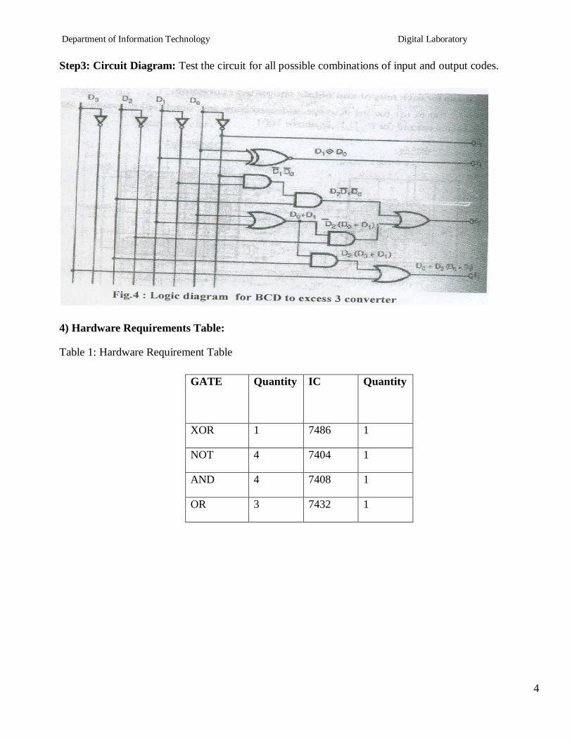
Department of Information Technology Digital Laboratory
4
Step3 Circuit Diagram Test the circuit for all possible combinations of input and output codes
4) Hardware Requirements Table
Table 1 Hardware Requirement Table
GATE Quantity
IC Quantity
XOR 1 7486 1
NOT 4 7404 1
AND 4 7408 1
OR 3 7432 1
Department of Information Technology Digital Laboratory
5
B Excess-3 To BCD Conversion
1 Truth Table
INPUT (EXCESS-3 CODE) OUTPUT (BCD CODE)
E3 E2 E1 E0 B3 B2 B1 B0
0 0 0 0 X X X X
0 0 0 1 X X X X
0 0 1 0 X X X X
0 0 1 1 0 0 0 0
0 1 0 0 0 0 0 1
0 1 0 1 0 0 1 01O6
51
0 1 1 0 0 0 1 1
0 1 1 1 0 1 0 0
1 0 0 0 0 1 0 1
1 0 0 1 0 1 1 0
1 0 1 0 0 1 1 1
1 0 1 1 1 0 0 0
1 1 0 0 1 0 0 1
1 1 0 1 X X X X
1 1 1 0 X X X X
1 1 1 1 X X X X
Department of Information Technology Digital Laboratory
6
2) K-Map For Reduced Boolean Expressions Of Each Output
Fig 5 K-Map For Reduced Boolean Expressions Of Each Output (BCD Code)
Department of Information Technology Digital Laboratory
7
3) Circuit Diagram Test the circuit for all possible combinations of input and output codes
4) Hardware Requirements Table
Table 2 Hardware Requirement Table
GATE Quantity
IC Quantity
XOR 1 7486 1
NOT 3 7404 1
AND 8 7408 2
OR 3 7432 1
Pin Diagrams
Department of Information Technology Digital Laboratory
8
7400 Quad 2-Input NAND Gate
7402 Quad 2-Input NOR Gate
7404 Not Gates
7408 Quad 2-Input AND Gates
7432 Quad 2-Input OR Gate
7486 Quad 2-Input Exclusive-OR Gate
Department of Information Technology Digital Laboratory
9
Conclusion
Thus we studied different codes and their conversions including applications
The truth tables have been verified using IC 7486 7432 7408 and 7404
FAQrsquos with answers
Q1) What is the need of code converters
There is a wide variety of binary codes used in digital systems Often it is required to convert from one
code to another For example the input to a digital system may be in natural BCD and output may be 7-
segment LEDs The digital system used may be capable of processing the data in straight binary format
Therefore the data has to be converted from one type of code to another type for different purpose
Q2) What is Gray code
It is a modified binary code in which a decimal number is represented in binary form in such a way that
each Gray- Code number differs from the preceding and the succeeding number by a single bit
(eg for decimal number 5 the equivalent Gray code is 0111 and for 6 it is 0101 These two codes differ
by only one bit position i e third from the left) It is non weighted code
Q3) What is the significance of Gray code
Important feature of Gray code is it exhibits only a single bit change from one code word to the next in
sequence Whereas by using binary code there is a possibility of change of all bits if we move from one
number to other in sequence (eg binary code for 7 is 0111 and for 8 it is 1000) Therefore it is more
useful to use Gray code in some applications than binary code
Q4) What are applications of Gray code
1 Important feature of Gray code is it exhibits only a single bit change from one code word to the next in
sequence This property is important in many applications such as Shaft encoders where error
susceptibility increases with number of bit changes between adjacent numbers in sequence
2 It is sometimes convenient to use the Gray code to represent the digital data converted from the analog
data (Outputs of ADC)
3 Gray codes are used in angle-measuring devices in preference to straight forward binary encoding
Department of Information Technology Digital Laboratory
10
4 Gray codes are widely used in K-map
Q5) What are weighted codes and non-weighted codes
In weighted codes each digit position of number represents a specific weight The codes 8421 2421 and
5211 are weighted codes Non weighted codes are not assigned with any weight to each digit position ie
each digit position within the number is not assigned a fixed value Gray code Excess-3 code are non-
weighted code
Q6) Why is Excess-3 code called as self-complementing code
Excess-3 code is called self-complementing code because 9rsquos complement of a coded number can be
obtained by just complementing each bit
Q7) What is invalid BCD
With four bits sixteen numbers (0000 to 1111) can be represented but in BCD code only 10 of these are
used as decimal numbers have only 10 digits fro 0 to 9 The six code combinations (1010 to 1111) are not
used and are invalid
Department of Information Technology Digital Laboratory
11
Regularity Content Viva-voce Timely
Submission Total
Dated Sign of
Subject
Teacher
2 4 2 2 10
Date of Performance Date of Completion
-------------------------------------------------------------------------------------------------------------------
Assignment No 2
------------------------------------------------------------------------------------------------------------------
Title BCD amp Excess 3 Adder
------------------------------------------------------------------------------------------------------------------
Objective 1 To study the BCD arithmetic rules
2 Comparison between binary and BCD codes
Problem Statement Design (truth table K-map) and implementation of 4-bit BCD to Excess-3 and
Excess-3 to BCD Code converters
-----------------------------------------------------------------------------------------------------------------
Hardware Requirement
i) IC 7483 (4 bit Binary adder) IC 7404(Hex INV) 7432 (OR-gate) 7408 (AND-gate)
ii) 7486 (EX-OR gate)
iii) Digital Trainer Kit -1
iv) Patch cords
----------------------------------------------------------------------------------------------------------------
Software Requirement Digital Work 30
------------------------------------------------------------------------------------------------------------------
Theory
BCD-Binary coded decimal-In this code each decimal digit represent by a 4-bit binary no BCD is a
way to express each of the decimal digits with binary code Positional weights associated to the binary bits
in BCD code are (MSB) 8-4-2-1(LSB)
BCD number 0 to 9 but greater than 9 is invalid BCD
Department of Information Technology Digital Laboratory
12
So Convert in valid BCD using add 6 ie (0110)
BCD Adder
BCD adder is a circuit that adds two BCD digits amp produces a sum of digits also in BCD
Rules for BCD addition
1 Add two numbers using rules of Binary addition
2 If the 4 bit sum is greater than 9 or if carry is generated then the sum is invalid To correct the sum
add 0110 i e (6)10 to sum If carry is generated from this addition add it to next higher order BCD
digit
3 If the 4 bit sum is less than 9 or equal to 9 then sum is in proper form
CASE I Sum lt= 9 amp carry = 0
Add BCD digits 3 amp 4
1 0 0 1 1
+ 0 1 0 0
------------
0 1 1 1
Answer is valid BCD number = (7)BCDamp so 0110 is not added
CASE II Sum gt 9 amp carry = 0
Add BCD digits 6 amp 5
1 0 1 1 0
+ 0 1 0 1
-----------
10 1 1
Department of Information Technology Digital Laboratory
13
Invalid BCD (since sum gt 9) so 0110 is to be added
2 1 0 1 1
+ 0 1 1 0
-----------
1 0 0 0 1
(1 1)BCD
Valid BCD result = (11) BCD
CASE III Sum lt = 9 amp carry = 1
Add BCD digits 9 amp 9
1 1 0 0 1
+1 0 0 1
-----------
1 0 0 1 0
Invalid BCD ( since Carry = 1 ) so 0110 is to be added
2 1 0 0 1 0
+ 0 1 1 0
------------
1 1 0 0 0
(1 8)BCD
Valid BCD result = (18) BCD
Design of BCD adder
1 To execute first step i e binary addition of two 4 bit numbers we will use IC 7483
( withCin = 0 ) which is 4 bit binary adder
2 We need to design a digital circuit which will sense sum amp carry of IC 7483 amp if sum exceeds 9 or
carry = 1 this digital circuit will produce high output otherwise its output will be zero
Circuit to check invalid BCD
Department of Information Technology Digital Laboratory
14
First we will design circuit to check sum amp then we will logically OR output of this circuit to carry
output of IC 7483
For digital circuit which we are going to design we will have 4 inputs
( S3 S2 S1 S0) amp only 1 output Y
a) Y output of this circuit Will be ORed with carry output of first adder IC
7483
b) If BCD result is invalid i e sum output of first 7483 we have to add
(6)10 ie (0110)2 that means we need one more binary adder IC 7483
c) If BCD result is valid ( ie final output of the circuit to check validity is 0) we will make an
arrangement that second adder IC 7483 adds (0)10 i e ( 0000 )2 to the sum of the first adder IC 7483
The output of the combinational circuit is used as final output carry amp carry output of second adder IC is
ignored
i ) Truth Table for design of combinational circuit for BCD adder to check invalid
BCD
K-map for output- Y=S3S2+S3S1
Department of Information Technology Digital Laboratory
15
iii) Circuit diagram
v) Hardware Requirements
GATE Quantity
IC Quantity
Binary adder 2 7483 2
AND 2 7408 1
OR 2 7432 1
B ) Design and Implement single digit EXCESS-3 adder using IC 7483
Excess-3 code is a non weighted code It is a modified form of a BCD code The Excess-3 code can be
derived from the natural BCD code by adding 3 to each coded number It is also known as Self
Complementary code
Excess-3 code is a self complementary code because 1rsquos complement of Excess-3 number is Excess-3
code for the 9rsquos complement of corresponding number
Output of BCD adder
Department of Information Technology Digital Laboratory
16
Eg Excess-3 code for (4)10 is (0111)XS-3 1rsquos complement of this number is 1000 which is Excess-3 code
for (5)10and 5 is 9rsquos complement of (4)10
Rules for Excess-3 addition
i Add two Exceess-3 numbers
ii If carry is 1 add 3 to Sum
iii If carry is 0 subtract 3 from sum
Eg (8)10 + (6)10
(8)10 = 1011 (Excess-3 for 8)
(6)10= 1001 (Excess-3 for 6)
_______________
1 0100
0011 0011
_______________
0100 0111 ( Excess 3 code for (14)10
(i)Design
1) 4 bit Binary addition of excess 3 codes of two operands can be implemented with IC 7483
2) We have to design the circuit which will either add 0011 or subtract 0011 ie add 1101 (2rsquos
complement of 0011)depending upon carry bit
Letrsquos compare 0011 and 1101
B3 B2 B1 B0
0 0 1 1 ------- When carry is 1
1 1 0 1 ------- When carry is 0
Here B0 bit in both situation is High
Now compare B3 B2 and B1 It is complement of each other
When carry is 1 Bit B1 =1 B2=B3=0
When carry is 0 Bit B1 =0 B2=B3=1
B1 bit follows the carry and B2 and B3 bit complements the carry
(ii) Circuit Diagram
Department of Information Technology Digital Laboratory
17
(iii ) HARDWARE REQUIREMENTS
Sl No IC Description Quantity
1 7404 Not Gate 01
2 7483 4 bit Binary Adder 04
CONCLUSION
BCD adder ampsubtractor is designed amp tested for all possible combinations
FAQrsquos
1 Explain and Write the significance of BCD number system
2 Write the applications of BCD amp Excess 3 code
3 Explain the rules of BCD amp Excess 3 arithmetic
4 What is the difference between BCD and binary codes
5 What do you mean by unpacked and packed BCD nos
Department of Information Technology Digital Laboratory
18
Regularity Content Viva-voce Timely
Submission Total
Dated Sign of
Subject
Teacher
2 4 2 2 10
+
Date of Performance Date of Completion
-------------------------------------------------------------------------------------------------------------------
Assignment No 3
---------------------------------------------------------------------------------------------------------------------------
Title Implementation of logic functions
----------------------------------------------------------------------------------------------------------------------
Objective 1 To study the difference between multiplexer demultiplexer and decoder
2To study the applications of multiplexer
---------------------------------------------------------------------------------------------------------------------
Problem Statement Implement of Logic function using multiplexer IC 74153
---------------------------------------------------------------------------------------------------------------------
Hardware Requirement
i) IC 74153 74138 7404 7432
ii) Digital Trainer Kit -1
iii) Patch cords
----------------------------------------------------------------------------------------------------------------
Software Requirement Digital Work 30
------------------------------------------------------------------------------------------------------------------
Theory
D CWigital Multiplexer
Multiplexer are combinational digital circuits equating as controlled switches with several data inputs (I0
I1 I2 hellip) amp one single data output (ldquooutrdquo)At any time one of the Ip is transmitted to output According to
binary signals applied on control pairs to circuit Usually the number of data inputs is a power of two
Multiplexing is the process of transmitting a large no of information units over a small no of channel
digital multiplexer is a combinational large circuit which performs the operation of multiplexing It selects
Department of Information Technology Digital Laboratory
19
the operation of multiplexing It selects the operation of binary information from one of the many input
lines amp transfer to a single op line Multiplexer is called a data selector or multiposition switch because it
selects one of the many input Selection of a particular line is controlled by a set of a selection lines or
selects inputs The number of select lines depends upon no of input lines Generally there
is lsquonrsquo selects line for lsquomrsquo input lines By applying a particular code on select lines is transmitted on the
output linesBlock diagram of MUX is shown at contains lsquo2mrsquo input lines lsquomrsquo select Such that 2m = n amp
one unable input which is used to activate or dedicate MUX Depending upon the no of IP amp OP lines
various types of multiplexers are available We have 21 41 81 161 MUX Here the first no indicates
the no of input lines amp second no indicates the no of output lines
E is called as enable input which is generally active low
Fig-Block diagram for N1 Multiplxer
Demultiplexer
Demultiplexer is a logic used to perform exactly reverse function performed by multiplexer It accepts a
single input and distributes among several outputs The selection of a particular output line is controlled
by a set of selection line There are n input lines amp 2m is the number of selection line whose bit
combinations determine which output to be selected
Encoder amp Decoder
1 Encoders are used to encode given digital number into different numbering format like
decimal to BCD Encoder Octal to Binary
2 Decoders are used to decode a coded binary word like BCD to seven segment decoder
3 Thus encoder and decoder are application specific logic develop we can not use any type of
input for any encoder and decoder
Smhelliphellips1 s0
Output(Y)
D0
D1
D2
D3
Dn
N1
multiplxer
E
Department of Information Technology Digital Laboratory
20
4 Need to select input according to encoder and decoder being selected for a particular
application as mention in examples above
Uses of Mux
1 Use for Boolean function implementation
2 Construct a common bus system
3 To select between multiple sources amp signal destination
4 Inter register transfer
Advantages
1) Simplification of logic expression not required
2) Logic design is simplified
Disadvantage
Only one function can be implemented using one MUX Hence they canrsquot be used in
combinational logic circuit which contains many function
Part-A (IC 74153)
1 VERIFICATION OF IC 74153
IC 74153 is a dual layer 41 MUX It has four input lines for (I0D-I3D) for second MUX amp active high
output lsquoYarsquo lsquoYbrsquo (1Y or 2Y) It has select lines S1S0 common to both MUX The Enable inputs are
active low EaampEb(1G and 2G) The MUX is activated when they are at logic o
Pin out of IC 74153
Department of Information Technology Digital Laboratory
21
Function table of IC 74153 (X= Donrsquot Care Condition)
Select Input
Inputs (I or II) Output
S1 S0 E (I or II) D0 D1 D2 D3 Y
X X 1 X X X X 0
0 0 0 0 X X X 0
0 0 0 1 X X X 1
0 1 0 X 0 X X 0
0 1 0 X 1 X X 1
1 0 0 X X 0 X 0
1 0 0 X X 1 X 1
1 1 0 X X X 0 0
1 1 0 X X X 1 1
2CASCADING OF IC 74153
Cascading is done to expand two or more MUX ICrsquos to a digital multiplexer with larger no of inputs ie
multiplexer stocks or tress is designed The enable input is used for cascading In case of IC 74153 we
have only two select lines But for certain application 3 select lines are required then it can be
obtained by cascading using enable Now with 3 select lines we have 8 combinations Out of this
combination the MSB is O MSB is 1 for last four combination so we can use these MSB to select
any 1 MUX out of two by connecting it to E pin of first 41 MUX
Function table of IC 74153 as 8 1 Mux by cascading 2 41 Mux
Select Input Output
C (1G 2G ) B (S1) A (S0) Y
0 0 0 D0
0 0 1 D1
0 1 0 D2
0 1 1 D3
1 0 0 D4
1 0 1 D5
Department of Information Technology Digital Laboratory
22
1 1 0 D6
1 1 1 D7
3FUNCTION IMPLEMENTATION
Y= sum m (1 3 5 6)
Thisexpression is in Standard SOP form and it is three variable function So we need to use mux with
three select inputs ie 81 Mux Already we have implemented 81 Mux using IC 74153 For Boolean
function in Standard SOP form we connect data inputs corresponding to the minterms present in the given
function to Vcc and remaining data inputs to ground
Truth table
Inputs Output
C B A Y
0 0 0 0
0 0 1 1
0 1 0 0
0 1 1 1
1 0 0 0
1 0 1 1
1 1 0 1
1 1 1 0
LOGIC DIAGRAM
Hardware Requirements
GATE Quantity
IC Quantity
Mux 1 74153 1
NOT 1 7404 1
OR 1 7432 1
Department of Information Technology Digital Laboratory
23
Part-B Decoder (IC 74138)
Theory
Discrete quantities of information are requested in digital system with binary codes A binary code of n
bits is capable of representing into 2n distinct elements of the coded information
Decoder converts coded input to coded outputs accepts one of the code
There are different types of decoders such as 38 decoder 416 line decoders etc These are in general
called as n m line decoder where m=2n and n= no of input lines and m=no of output lines Demux also
takes one input data line source and selectively distributes it to one of n output channels The only
difference between demux and decoder is that demux has Din (data ip) line whereas decoder does not
have
ADVANTAGES
1) The decoder provides best implementation whenever there are many outputs of the combinational
circuit and each op of the function (or its complement) is required to be expressed with a small no
of minterms
2) The decoder can function as demux If the Enable ip line is taken as Din (data ip)
DISADVANTAGES
Since decoder method requires an OR gate for each op function so there is new hardware used And it is
always advisable to use minimum hardware as we come across problems like propagation delay of gates
APPLICATIONS
Decoder is worthily used for decoding binary information and memory interfacing It is used for the
implementation of Boolean function
Differentiate between Mux Demux Decoder
Point Multiplexer Demultiplexer Decoder
Input Many input lines Single input line Many input line also Acts as select line
Output Single output line Many output line Many output lineActive low output
Select line 2m = n n = 2m Enable inputs used
Department of Information Technology Digital Laboratory
24
A) Verification of IC 74138
We use IC 74138 which accepts 3 binary weighted inputs (A0 A1 A2) and when enabled provides
mutually exclusive active low outputs (y0-y7) It features 3 Enable ips Two active low (G2A G2B) and
one active high (G1) Every output will be high unless G2A G2Bare low and G1 is high It has
demultiplexing capability and multiple enable ips for easy expansion
IC Diagram
Function Table of 38 decoder
Input Output
Enable Data
G2A G2B G1 A2 A1 A0 Y0 Y1 Y2 Y3 Y4 Y5 Y6 Y7
0 0 0 X X X 1 1 1 1 1 1 1 1
0 1 1 X X X 1 1 1 1 1 1 1 1
1 0 1 X X X 1 1 1 1 1 1 1 1
1 1 1 X X X 1 1 1 1 1 1 1 1
Department of Information Technology Digital Laboratory
25
0 0 1 0 0 0 0 1 1 1 1 1 1 1
0 0 1 0 0 1 1 0 1 1 1 1 1 1
0 0 1 0 1 0 1 1 0 1 1 1 1 1
0 0 1 0 1 1 1 1 1 0 1 1 1 1
0 0 1 1 0 0 1 1 1 1 0 1 1 1
0 0 1 1 0 1 1 1 1 1 1 0 1 1
0 0 1 1 1 0 1 1 1 1 1 1 0 1
0 0 1 1 1 1 1 1 1 1 1 1 1 0
B) Cascading of IC 74138
The enable ip G1 active high of IC 74138 is used for cascadingfor cascading 2 ICrsquos the enable ip G1 of
first IC is connected to G1 enable ip of second IC through a NOT gate This enable ip is used as MSB
select ip line A3 the other three select input lines of both ICrsquos (A0A1A2) are also shorted to select
input lines of second IC to get single ip select lines (A0A1A2)
The ip line A3 is used to enable disable the 2 IC 74138 decoders When A3=0 first IC is enabled and
second is disabled Thus the first decoder will generate minterms from 0000 to 0111 as op and the second
decoder will generate nothing When A3=1 the enable conditions are reversed and thus second decoder
IC will generate minterms 1000 to 1111
Function Table of 416 decoder using IC 74138 (38 decoder)
Input Output
Enable Data
G2
A
G2
B
A
3
A
2
A
1
A
0
Y
0
Y
1
Y
2
Y
3
Y
4
Y
5
Y
6
Y
7
Y
8
Y
9
Y1
0
Y1
1
Y1
2
Y1
3
Y1
4
Y1
5
0 1 X X X X 1 1 1 1 1 1 1 1 1 1 1 1 1 1 1 1
Department of Information Technology Digital Laboratory
26
1 0 X X X X 1 1 1 1 1 1 1 1 1 1 1 1 1 1 1 1
1 1 X X X X 1 1 1 1 1 1 1 1 1 1 1 1 1 1 1 1
0 0 0 0 0 0 0 1 1 1 1 1 1 1 1 1 1 1 1 1 1 1
0 0 0 0 0 1 1 0 1 1 1 1 1 1 1 1 1 1 1 1 1 1
0 0 0 0 1 0 1 1 0 1 1 1 1 1 1 1 1 1 1 1 1 1
0 0 0 0 1 1 1 1 1 0 1 1 1 1 1 1 1 1 1 1 1 1
0 0 0 1 0 0 1 1 1 1 0 1 1 1 1 1 1 1 1 1 1 1
0 0 0 1 0 1 1 1 1 1 1 0 1 1 1 1 1 1 1 1 1 1
0 0 0 1 1 0 1 1 1 1 1 1 0 1 1 1 1 1 1 1 1 1
0 0 0 1 1 1 1 1 1 1 1 1 1 0 1 1 1 1 1 1 1 1
0 0 1 0 0 0 1 1 1 1 1 1 1 1 0 1 1 1 1 1 1 1
0 0 1 0 0 1 1 1 1 1 1 1 1 1 1 0 1 1 1 1 1 1
0 0 1 0 1 0 1 1 1 1 1 1 1 1 1 1 0 1 1 1 1 1
0 0 1 0 1 1 1 1 1 1 1 1 1 1 1 1 1 0 1 1 1 1
0 0 1 1 0 0 1 1 1 1 1 1 1 1 1 1 1 1 0 1 1 1
0 0 1 1 0 1 1 1 1 1 1 1 1 1 1 1 1 1 1 0 1 1
0 0 1 1 1 0 1 1 1 1 1 1 1 1 1 1 1 1 1 1 0 1
0 0 1 1 1 1 1 1 1 1 1 1 1 1 1 1 1 1 1 1 1 0
C) Implementation of Boolean function
The procedure for implementation of combinational circuit by means of a decoder and lsquoORrsquo gates requires
that the Boolean function fir the circuit be expressed in Sum of Minterms These forms can be obtained by
Department of Information Technology Digital Laboratory
27
expanding the function A decoder is then chosen which generates all the minterms of n ip variables The
ip to each OR gate are selected from the decoder outputs according to the minterms list in each function
i) F1=summ (1 3 5 7)
Truth table
Logic Diagram
ii) F2=summ (1 3 5 7111315)
Truth table
Logic Diagram
Conclusion In this way multiplexer Decoderamp its applications are studied implemented amp
tested
FAQrsquos
1What is a multiplexer
2What is a Demultiplexer
3 Enlist applications of multiplexer
Department of Information Technology Digital Laboratory
28
Regularity Content Viva-voce Timely
Submission Total
Dated Sign of
Subject
Teacher
2 4 2 2 10
Date of Performance Date of Completion
-------------------------------------------------------------------------------------------------------------------
Assignment No4
------------------------------------------------------------------------------------------------------------------
Title 3 bit updown Asynchronous and Synchronous counter using IC7476
------------------------------------------------------------------------------------------------------------------
Objective To understand design procedure of asynchronousamp Synchronous counter
------------------------------------------------------------------------------------------------------------------
Problem Statement Design (State diagram state table amp K map) and implementation of 3
bit Up and Down Asynchronous and Synchronous Counter using master slave JK flip-flop IC 7476
-----------------------------------------------------------------------------------------------------------------
Hardware Requirement
i) IC 7476 (MS-JK Flip-flop) IC 7408(Quad 2 ip AND Gate)
IC 7432 (Quad 2 ip OR Gate) and IC 7404 (Hex Inverter)
ii) Digital Trainer Kit -132
iii) Patch cords
----------------------------------------------------------------------------------------------------------------
Software Requirement Digital Work 30
------------------------------------------------------------------------------------------------------------------
Theory
Counters counters are logical device or registers capable of counting the no of states or no of clock
pulses arriving at its clock input where clock is a timing parameter arriving at regular intervals of time
so counters can be also used to measure time amp frequencies They are made up of flip flops Where the
Department of Information Technology Digital Laboratory
29
pulse are counted to be made of it goes up step by step amp the op of counter in the flip flop is decoded to
read the count to its starting step after counting n pulse incase of module counters
Types of Counters
Counter are of two types
1) Asynchronous counter
2) Synchronous counter
Asynchronous counter
A digital counter is a set of flip flop The flip flop are connected such that their combined state at any time
is binary equivalent of total no of pulses that have occurred up to that time Thus its name implies a
counter is used to count pulse A counter is used as frequency dividers To obtain waveform with
frequency that is specific fraction of clock frequency
Counter may be Asynchronous or synchronous The Asynchronous counter is also called as ripple counter
An Asynchronous counter uses T flip flop to perform a counting function The actual hardware used is
usually J-K flip flop with J amp K connected to logic1Even D flip flops may be used here
In asynchronous counter commonly called ripple counter the first flip-flop is clocked by the external
clock pulse amp then each successive flip-flop is clocked by the Q or Qrsquo output of the previous flip-flop
Therefore in an asynchronous counter the flip-floprsquos are not clocked simultaneously The input of MS-JK
is connected to VCC because when both inputs are one output is toggled As MS-JK is negative edge
triggered at each high to low transition the next flip-flop is triggered
Synchronous Counter
When counter is clocked such that each flip flop in the counter is
triggered at the same time the counter is called as synchronous counter
The gates propagation delay at reset time will not be present or we may say will not occur
1) Asynchronous Up Counter
Fig 1 shows 3bit Asynchronous Up Counter Here Flip-flop 2 act as a MSB Flip-flop and Flip-flop 0 act
as a LSB Flip-flop Clock pulse is connected to the Clock of Flip-flop 0 Output of Flip-flop 0(Q0) is
connected to clock of next flip-flop (ie Flip-flop 1) and so on As soon as clock pulse changes output is
going to change (at the negative edge of clock pulse) as a Up count sequence For 3 bit Up counter state
table is as shown below
Department of Information Technology Digital Laboratory
30
State Table
Logic diagram
Fig 1 3 Bit Asynchronous Up Counter
Hardware requirements
Gate
Flip flop
Quantity IC Quantity
MS JK 3 7476 2
2) Down Counter
Fig 2 shows 2 bit Asynchronous Down Counter Here Flip-flop 2 act as a MSB Flip-flop and Flip-flop 0
act as a LSB Flip-flop Clock pulse is connected to the Clock of Flip-flop 0 Output of Flip-flop 0 (Q0rsquo) is
Counter States Count
Q2 Q1 Q0
0 0 0 0
1 0 0 1
2 0 1 0
3 0 1 1
4 1 0 0
5 1 0 1
6 1 1 0
7 1 1 1
8 0 0 0
Department of Information Technology Digital Laboratory
31
connected to clock of next flip-flop (ie Flip-flop 1) and so on As soon as clock pulse changes output is
going to change (at the negative edge of clock pulse) as a down count sequence For 3 bit down counter
sate table is as shown below
In both the counters Inputs J and K are connected to Vcc hence J-K Flip flop work in toggle mode Preset
and Clear both are connected to logic 1
State Table
Logic diagram
Fig 2 3 Bit Asynchronous Down Counter
Hardware requirements
Counter States Count
Q2 Q1 Q0
7 1 1 1
6 1 1 0
5 1 0 1
4 1 0 0
3 0 1 1
2 0 1 0
1 0 0 1
0 0 0 0
7 1 1 1
Department of Information Technology Digital Laboratory
32
Gate
Flip flop
Quantity IC Quantity
MS JK 3 7476 2
Applications
The asynchronous counters are specially used as the counting devices
They are also used to count number of pulses applied
It also works as frequency divider
It helps in counting the number of product coming out of the machinery where product is coming out at
equal interval of time
Types of synchronous counter
1) Up counter
2) Down counter
1 3 bit Synchronous up counter
The up counter counts from 0 to7 ie(000 to 111)for this we are using MS JK flip flop In IC 74LS76 2
MS J-K flip flops are present The clock pulse is given at pin 1 amp 6 of the 1st IC amp pin 1 of 2nd IC Next
state decoder logic is designed with the help of state table
State table for synchronous up counter
Present state Next state Flip flop 3 Flip flop 2 flip flop 1
Q2 Q1 Q0 Q2 Q2 Q0 J2 K2 J1 K1 J0 K0
0 0 0 0 0 1 0 x 0 X 1 x
0 0 1 0 1 0 0 x 1 X x 1
0 1 0 0 1 1 0 x x 0 1 x
0 1 1 1 0 0 1 x x 1 x 1
1 0 0 1 0 1 x 0 0 X 1 X
1 0 1 1 1 0 x 0 1 X x 1
1 1 0 1 1 1 x 0 x 0 1 X
1 1 1 0 0 0 x 1 x 1 x 1
Department of Information Technology Digital Laboratory
33
K-Map
Q1Q0
Q2
00 01 11 10
0 0 0 1 0
1 X X X X
J2= Q1Q0
Q1Q0
Q2
00 01 11 10
0 X X X X
1 0 0 1 0
K2= Q1Q0
Q1Q0
Q2
00 01 11 10
0 0 1 X X
1 0 1 X X
J1= Q0
Q1Q0
Q2
00 01 11 10
0 X X 1 0
1 X X 1 0
K1= Q0
Department of Information Technology Digital Laboratory
34
Q1Q0
Q2
00 01 11 10
0 1 X X 1
1 1 X X 1
J0= 1
Q1Q0
Q2
00 01 11 10
0 X 1 1 X
1 X 1 1 X
K0= 1
Logic Diagram
Fig 1 3 bit Synchronous up counter
Department of Information Technology Digital Laboratory
35
2 3 bit Synchronous down counter
This is used to count from 7-0 ie(111-000)for this also 2 ICrsquos of 74LS76 are required amp hence we use 3
MS JK flip flops Here also clock is given to 1stamp 6th pin of 1st IC amp1st pin of 2nd IC enabling to apply
clock to all flip flop at a time Next state decoder logic is designed with the help of state table
State table for synchronous down counter
Present state Next state Flip flop 3 Flip flop 2 Flip flop 1
Q2 Q1 Q0 Q2 Q1 Q0 J2 K2 J1 K1 J0 K0
1 1 1 1 1 0 X 0 X 0 X 1
1 1 0 1 0 1 X 0 X 1 1 X
1 0 1 1 0 0 X 0 0 X X 1
1 0 0 0 1 1 X 1 1 X 1 X
0 1 1 0 1 0 0 X X 0 X 1
0 1 0 0 0 1 0 X X 1 1 X
0 0 1 0 0 0 0 X 0 X X 1
0 0 0 1 1 1 1 X 1 X 1 X
K-Map
Q1Q0
Q2
00 01 11 10
0 1 0 0 0
1 X X X X
J2= Q1Q0
Q1Q0
Q2
00 01 11 10
Department of Information Technology Digital Laboratory
36
0 X X X X
1 1 0 0 0
K2= Q1Q0
Q1Q0
Q2
00 01 11 10
0 1 0 X X
1 1 0 X X
J1= Q0
Q1Q0
Q2
00 01 11 10
0 X X 0 1
1 X X 0 1
K1= Q0
Q1Q0
Q2
00 01 11 10
0 1 X X 1
1 1 X X 1
J0= 1
Q1Q0
Q2
00 01 11 10
0 X 1 1 X
1 X 1 1 X
K0= 1
Department of Information Technology Digital Laboratory
37
Logic Diagram
Fig 2 3 bit Synchronous down counter
Uses
1 Specially used as the counting devices
2 Used in frequency divider circuit
3 Used in digital voltmeter
4 Used in counter type A to D converter
5 Used for time measurement
6 It helps in counting the no of product coming out from machinery where product is coming out
at equal interval of time
Conclusion
Up and down counters are successfully implemented the counters are studied amp op are checked The
state table is verified
PRACTICE ASSIGNMENTS EXERCISE MODIFICATIONS
1 Design amp implement 2 bit controlled synchronous counter
2 Designamp implement 4 bit controlled synchronous counter
3 Designamp implement truncated synchronous up or down counter
FAQrsquos with answers
1 What do you mean by Counter
A Counter is a register capable of counting the no of clock pulses arriving at its
clock inputs Count represents the no of clock pulses arrived A specified
sequence of states appears as the counter output
Department of Information Technology Digital Laboratory
38
2 What are the types of Counters Explain each
There are two types of counters as Asynchronous Counter and Synchronous Counter
Asynchronous Counter In this counter the first flip-flop is clocked by the external clock pulse
and then each successive flip-flop is clocked by the Q or Qrsquo op of the previous flip-flop Hence in
Asynchronous Counter flip-flops are not clocked simultaneously and hence called as Ripple
Counter Synchronous Counter In this counter the common clock input is connected to all the
flip-flops simultaneously
3 What do you mean by pre-settable counters
A counter in which starting state is not zero can be designed by making use of the
preset inputs of the flip flops This is referred to as loading the counter
asynchronously This is referred to as pre-settable counter
4 What are the applications of synchronous counters
Digital clock
Frequency divider circuits
Frequency counters
Used in analog to digital converters
5 What are the advantages of synchronous counters over asynchronous counters
Propagation delay time is reduced
Can operate at a much higher frequency than the asynchronous counters
6 Ring counter is an example of synchronous counters or asynchronous counter
Synchronous counter Since all the flip flops are clocked simultaneously
7 Twisted Ring (Johnsonrsquos) counter is an example of synchronous counters or asynchronous
counter
Synchronous counter Since all the flip flops are clocked simultaneously
8 What is the difference between ring counter and twisted ring counter
In ring counter pulses to be counted are applied to a counter it goes from state to state and the
output of the flip flop s in the counter is decoded to read the count Here the uncomplimentary
output (Q) of last flip flop is fed back as an input to first flip flop Ring counters are referred as
MOD lsquoNrsquo counters
Department of Information Technology Digital Laboratory
39
But in Twisted ring counter the complimentary output (Q bar) of last flip flop is fed back as an
input to first flip flop Twisted Ring counters are referred as MOD lsquo2Nrsquo counters
9 What are the applications of ring counters
Ring counter outputs are sequential non-overlapping pulses which are useful for control state
counters Used in stepper motor this requires pulses to rotate it from one position to the next Used
as divide by lsquoNrsquo ((MOD lsquoNrsquo) counters
10 What are the applications of ring counter twisted ring counters
Used as divide by lsquo2Nrsquo ((MOD lsquo2Nrsquo) counters
Used for control state counters
Used for generation of multiphase clock
11 List the Synchronous Counter ICs
IC 74160 Decade Up Counter
IC 74161 4 bit binary Up Counter
IC 74162 Decade Up Counter
IC 74163 4 bit binary Up Counter
IC 74168 Decade UpDown Counter
IC 74169 4 bit Binary UpDown Counter
IC 74190 Decade UpDown Counter
IC 74191 4 bit Binary UpDown Counter
IC 74192 Decade UpDown Counter
IC 74193 4 bit Binary UpDown Counter
Department of Information Technology Digital Laboratory
40
Regularity Content Viva-voce Timely
Submission Total
Dated Sign of
Subject
Teacher
2 4 2 2 10
Date of Performance Date of Completion
-------------------------------------------------------------------------------------------------------------------
Assignment No 5
-------------------------------------------------------------------------------------------------------------------------------
Title Design and implementation of Module lsquonrsquo counter with IC7490 and IC 74191
-----------------------------------------------------------------------------------------------------------------------------
Objective To know difference between regular amp truncated counter as well as binary ampBCD Counter
--------------------------------------------------------------------------------------------------------------------------------
Problem Statement To design and implement mod - 10 mod ndash 7 mod - 99 asynchronous BCD
counter using IC 7490 and to design and implement up down mod - n Binary counter using IC 74191
-----------------------------------------------------------------------------------------------------------------
Hardware Requirement
i) IC 7490 IC 74191 basic gates
ii) Digital Trainer Kit -1
iii) Patch cords
----------------------------------------------------------------------------------------------------------------
Software Requirement Digital Work 30
------------------------------------------------------------------------------------------------------------------
Theory
Part A ndash IC 7490
IC 7490 is a TTL MSI (medium scale integration) decade counter It contains 4 master slave flip flops
internally connected to provide MOD-2 ie divide by 2 and MOD-5 ie divide by 5 counters MOD-2 and
Mod-5 counters can be used independently or in cascading
Department of Information Technology Digital Laboratory
41
It is a 4-bit ripple type decade counter The device consists of 4-master slave flip flops internally
connected to provide a divide by two and divide by 5 sections Each section has a separate clock ip to
initiate state changes of the counter on the high to low clock transition
Since the op from the divide by 2 section is not internally connected to the succeeding stages The device
may be operated in various counting modes In a BCD counter the CP1 input must be externally connected
to QA op The CP0ip receives the incoming count producing a BCD count sequence It is also provided
with additional gating to provide a divide by 2 counter and binary counter for which the count cycle length
is divide by 5 The device may be operated in various counting modes
There are 2 reset inputs R0(1) and R0(2) both of which need to be connected to the lsquologic 1rsquo for clearing all
flip flops Two set inputs Rg(1) and Rg(2) when connected to logic 1 are used for setting counter to 1001
(BCD 9)
Pin out of IC 7490
Fig Pin configuration of IC7490
Table 1-pin name and description of IC7490
Pin name Description
Input B This is clock input to the internal MOD-5 ripple counter which is negative
edge triggered
R0(1)R0(2) Gated zero reset inputs
Department of Information Technology Digital Laboratory
42
R9(1)R9(2) These are gated set to nine inputs
QDQCQB Output of internal MOD-5 counter with QD as MSB
QA Output of internal MOD-2 counter with QA as LSB
Input A Clock input to FF-A which is negative edge triggered
Functional Table for IC7490
Reset inputs Output
R0(1) R0(2) R9(0) R9(1) QD QC QB QA
1 1 0 X 0 0 0 0
1 1 X 0 0 0 0 0
X X 1 1 1 0 0 1
X 0 X 0 COUNTER
0 X 0 X COUNTER
0 X X 0 COUNTER
X 0 0 x COUNTER
Department of Information Technology Digital Laboratory
43
Basic internal Structure of IC 7490
Function Table of MOD-5 counter
Design of MOD-10 counter using IC 7490
The QA op the first flip flop is connected to the input B which is clock ip of internal MOD-5 ripple
counter Due to cascading of Mod-2 and Mod-5 counters the overall configuration the decade counters
count from 0000 to 1001 After 1001 mod-5 resets to 0000 and next count after 1001 is 0000
When QA op is connected to B ip we have the Mod-2 counter followed by Mod-5 counter The
count sequence obtained is shown in the table It may be noted that QA changes from 0 to 1 the state of
InputB clock Output
Count QD QC QB
0 0 0 0
0 0 1 1
0 1 0 2
0 1 1 3
1 0 0 4
Department of Information Technology Digital Laboratory
44
Mod-5 counter doesnrsquot change whereas when QA changes from 1 to 0 the Mod-5 counter goes to the next
state
Logic DiagramMOD-10 counter using IC 7490
5 Modulus n Counter
Function table
Ip clock
Output
Count QD QC QB QA
0 0 0 0 0
0 0 0 1 1
0 0 1 0 2
0 0 1 1 3
0 1 0 0 4
Department of Information Technology Digital Laboratory
45
Design of Mod-7 Counter using IC 7490
Mod-7 counter counts through seven states from 0 to 6 counters and it should reset as soon as the
count becomes 7 The op of reset logic should be 1 corresponding to invalid states The reset logic op
should be applied to pin 2 and 3
Truth Table of Reset Logic
0 1 0 1 5
0 1 1 0 6
0 1 1 1 7
1 0 0 0 8
1 0 0 1 9
QD QC QB QA Y
0 0 0 0 0
0 0 0 1 0
0 0 1 0 0
0 0 1 1 0
0 1 0 0 0
0 1 0 1 0
0 1 1 0 0
0 1 1 1 1
1 0 0 0 1
1 0 0 1 1
Department of Information Technology Digital Laboratory
46
Logic Diagram Mod 7 Counter using IC 7490
Function table
Ip clock
Output
Count QD QC QB QA
0 0 0 0 0
0 0 0 1 1
0 0 1 0 2
0 0 1 1 3
0 1 0 0 4
0 1 0 1 5
0 1 1 0 6
Department of Information Technology Digital Laboratory
47
Design of Mod-99 using IC 7490
For Mod-99 two IC 7490rsquos will be required Hence to implement a divide by 99 counter we have
to use two decade counters ICrsquos A divide by 99 counter counts 99 states from 0 to 98 and the counter
should reset as soon as the count becomes 99 So in order to reset the counter of 99 connect the Q op
which are equal to 1 in the count of 99 to an lsquoAndrsquo gate amp then connect and op to the reset ip of both
ICrsquos
MOD-100 Counter-
MOD-100 counter can be obtained by cascading two decade counter ICrsquos
Each IC gives divide by 10 counts Hence 2 ICs will give 1010=100 counts
Clock is applied to the input A of IC 7490 the Q1 output is connected to B input etc
For cascading the QD output of the first IC is connected to the input A of second IC Thus QD of
IC-(1) acts as clock input to IC-(2)
The Ro (1) Ro(2) R9(1) R9(2) inputs of both ICs are connected to ground so as to make them
inactive
The total count provided by the two counters varies from 00 to 99 decimal that means 100 states
Hence it is a MOD-10 counter
Impleacutementations
FigureMOD-100 counters using IC 7490
Department of Information Technology Digital Laboratory
48
B) IC 74191 ndash Theory
IC74191 is 4-bit binary synchronous reversible up down counter It contains 4 master slave flip flops
with internal gating and steering logic to provide asynchronous reset and synchronous count updown
operations its asynchronous parallel capability permits the counter to be preset to any desire number D0
to D3 are the parallel data inputs Information present on the parallel data inputs D0 to D3 is loaded into
the counter and appears on the output when the load PLinput is lowThisoperation overrides the counting
function Counting is inhabited by the high level on the enable G input when G input is low internal state
changes are initiated synchronously by the low to high transitions of the clock inputs the updown input
signal determines the direction of input
Function Table
Operating
mode
Inputs Outputs
PL UD G CLK Dn
Parallel
load L X X X L L
L X X X H H
Count up H L 0 uarr X Count up
Count
down H H 0 uarr X
Count
down
Hold(No
change) H X H X X No change
Pin details ndash
D0 to D3 input lines PL parallel load
G is Enable input ndash enabling the counting
Q0 to Q3 output lines
Downup determines the direction of counting
Clk clock input for counter
Terminal Count Max(1111) min(0000) For these states signal goes high for 1clock pulse
Ripple clock Clock input for next higher state
Department of Information Technology Digital Laboratory
49
Pin Diagram IC 74191
Up counter- Truth Table
Clk
Pulses QA QB QC QD
0 0 0 0 0
1 0 0 0 1
2 0 0 1 0
3 0 0 1 1
4 0 1 0 0
5 0 1 0 1
6 0 1 1 0
7 1 1 1 1
8 1 0 0 0
9 1 0 0 1
10 1 0 1 0
11 1 0 1 1
12 1 1 0 0
13 1 1 0 1
Department of Information Technology Digital Laboratory
50
14 1 1 1 0
15 1 1 1 1
Logic Diagram
Steps-
Connect the circuit as shown above
Apply clock ip to pin no14
Connect UD to GND
Verify the output according to truth table
Logic diagram of down counter
Steps-
Connect the circuit as shown above
Apply clock ip to pin no14
Connect UD to VCC
Verify the output according to truth table
UD D3 D2 D1 D0 PL
Clock IC 74191
G RC
MAX MIN
Q3 Q2 Q1 Q0 TC
vcc
NC
NC
Outputs
no connection
vcc
Department of Information Technology Digital Laboratory
51
With the help of IC74191 we can implement truncated updown counter by using following logic ndash
Connect data input line to particular count you want to load
According to requirement make Truth table
Draw the K-map
Find out Boolean expression
Draw the logic diagram and that is the combinational logic for your count and apply the output of
that circuit to PL
According to requirement we get the UP and down counting
5 Modulus n Counter
Presettable updown counter
Mod 11 counter
Implementation of presetttable mod updown counter using IC- 74LS191
1 Load Data on data lines D0 to D3 (0101)
2 Counter will go through the states from 0101 0110hellip1111 in up counter and 0101 to 0000 in
down counter
Combinational Circuit
CLOCK D3 D2 D1 D0
TC
U D 74191 RC
G PL
Updown Q3 Q2 Q1 Q0 PL
Q3 Q2 Q1 Q0
Preset Count
Department of Information Technology Digital Laboratory
52
3 The logic circuit should be designed in such a way that only when all the outputs are high output
of the reset circuit should be low and the counter should jump to state 5 It should again start
counting from 0101 to 0000
State Table
Down Counter UP Counter
IC 74191 is 4 bit counter Thus it counts 0000 to 1111 different 16 states For MOD11 counter we require
different 11 states so 5 steps must be skipped from 16 states We get MOD11 by presetting counter to
value 5
Assignment Question
Design and Implement MOD 7 MOD 10 and MOD 12 using IC 74191
FAQs
1 What do you mean modulus counter
Counter
state Clock
pulse
Q3 Q2 Q1 Q0
1 0 1 0 1
2 0 1 1 0
3 0 1 1 1
4 1 0 0 0
5 1 0 0 1
6 1 0 1 0
7 1 0 1 1
8 1 1 0 0
9 1 1 0 1
10 1 1 1 1
11 1 1 1 1
Counter state
Clock pulse
FF outputs
Q3 Q2 Q1 Q0
1 0 1 0 1
2 0 1 0 0
3 0 0 1 1
4 0 0 1 0
5 0 0 0 1
6 0 0 0 0
7 0 1 0 1
Department of Information Technology Digital Laboratory
53
It represents the number of possible states of counter
2 How will you use the 7490 IC to design symmetrical divide by 10 frequency counter
The divide by 5 circuit followed by divide by 2 circuit will give symmetrical output
3Where counters are used Give real life example of counter
Modulus n Counter
Binary counter ndash An N stage counter that recycles after 2 Ncount The count proceds in specified binary
sequence Counter Presetable- A counter which can be set to a desired value before the start of the
counting UPDown counter ndash A counter that can count in both up and down direction depending upon a
control input
Department of Information Technology Digital Laboratory
54
Regularity Content Viva-voce Timely
Submission Total
Dated Sign of
Subject
Teacher
2 4 2 2 10
Date of Performance Date of Completion
-------------------------------------------------------------------------------------------------------------------
Assignment No6
------------------------------------------------------------------------------------------------------------------
Title Sequence Generator
------------------------------------------------------------------------------------------------------------------
Objective To understand sequence generator one of the sequential circuit
-------------------------------------------------------------------------------------------------------------------
Problem Statement Design (State Diagram State Table K Map) and implementation of Sequence
Generator using Shift Register IC 74194
-----------------------------------------------------------------------------------------------------------------
Hardware Requirement
i) IC 741947408 (AND-gate) 7432 (OR-gate)
ii) Digital Trainer Kit -1
iii) Patch cords
----------------------------------------------------------------------------------------------------------------
Software Requirement Digital Work 30
------------------------------------------------------------------------------------------------------------------
Theory
Part A Sequence Generator with Flip flop
A sequential circuit which generates a prescribed sequence of bits in synchronism with a clock is referred
to as a sequence generator These pulse trains or sequence of bits can be used to open valves close gates
turn on lights and turn off machines and other variety of jobs
Department of Information Technology Digital Laboratory
55
For the design of sequence generator we first determine the required no of flip flops and the logic circuit
for the next state decoder
No of flip flops required to generate particular sequence can be determined as follows
1) Find the no of 1rsquos in the sequence
2) Find the no of 0rsquos in the sequence
3) Take the maximum out of two
4) If N is the required no of flip flops choose minimum value of lsquonrsquo to satisfy equation given below
Max (0rsquos 1rsquos) le 2n-1
The sequence generator can be classified as
1) sequence generator without bushing
2) sequence generator with bushing
The aim in this experiment is to design a sequence generator to generate a sequence of bit ie 10101
Part B Sequence Generator using Shift Register IC 74194
IC 74194 4 bit bidirectional Shift Register
This bidirectional shift register is designed to incorporate virtually all the features a system designer may
want in a shift register they feature Parallel inputs parallel outputs right shift left shift serialinputs
operating mode control inputsand a direct overriding clear line The register has four distinct modes of
operationsnamely
1 Parallel load
2 Shift right (in the direction QA towards QD)
3 Shift left (in the direction QD towards QA)
4 Inhibit clock (do nothing)
Synchronous parallel loading is accomplished by applying the four bits of data and taking both
mode control inputs S0 and S1High The data is loaded in to the associated flip-flops and appear
at the outputs after positive transition of the clock input During loading serial data flow is
inhibited
Shift right is accomplished synchronously with the rising edge of the clock pulse when S0 is High
and S1 is Low Serial data for this mode is entered at the shift right data input When S0 is Low
and S1 is High data shifts left synchronously and new data is entered at the shift left serial input
Clocking of the flip flop is inhibited when both mode control inputs are LOW
Department of Information Technology Digital Laboratory
56
Mode Control Input Operation
S1 S0
0 0 Clock Inhibit
0 1 Shift right
1 0 Shift Left
1 1 Parallel loading
Function Table of IC 74194
Design
The minimum number of flip-flops N required to generate a sequence of length S is given by S
le 2N ndash 1
In this case S=7 therefore the minimum value of N which may generate in this sequence is 3
However it is not guaranteed to lead to a solution If the given sequence leads to seven distinct
states then only three flip flops are sufficient otherwise we have to increase the number of flip
flops We write the states of circuit as given in table 1 The prescribed sequence is listed under QA
and the sequence listed under QB and QC are the same sequence delayed by one and two clock
pulses respectively From the table we observe that all the states are not distinct which means N=3
is not sufficient Next we assume that N=4 and prepare table 2 The last column gives the required
serial input for getting the desired change of state when a clock pulse is applied This is obtained
by assuming D type flip flop and looking at the QA output For example at the falling edge of first
clock pulse QA=1 The second clock pulse must result in QA=1 which requires its D input to be 1
In the same manner all the entries in column Y are determined
Table 1 State Assignment Table of Sequence Generator (N=3)
Number of Clock
Pulses
Flip Flop Inputs States
QA QB QC
1 1 1 1 7
2 1 1 1 7
3 0 1 1 3
4 1 0 1 5
Department of Information Technology Digital Laboratory
57
5 0 1 0 2
6 1 0 1 5
7 1 1 0 6
Excitation table of D Flip-Flop
Present State Qn Next State Qn+1 Flip-Flop Input D
0 0 0
0 1 1
1 0 0
1 1 1
Table 2State Assignment Table of Sequence Generator (N=4)
Number of Clock
Pulses
Flip Flop Inputs States
Y
Serial ip QA QB QC QD
1 1 1 1 0 14 1
2 1 1 1 1 15 0
3 0 1 1 1 7 1
4 1 0 1 1 11 0
5 0 1 0 1 5 1
6 1 0 1 0 10 1
7 1 1 0 1 13 1
K-Map Simplification
Department of Information Technology Digital Laboratory
58
00 01 11 10
00 X X X X
01 X 1 1 X
11 X 1 0 1
10 X X 0 1
Y= QArsquo + QBrsquo + QCrsquo = QAQBQC
LOGIC DIAGRAM
HARDWARE REQUIREMENTS
Sr no ICs Description Quantity
11 74194 4 bit bidirectional universal shift register 16ktr`
2 7410 3 input NAND Gate 1
Department of Information Technology Digital Laboratory
59
Conclusion In this way sequence generator using JK flip flips amp shift register is designed and
implemented
Enhancements Modifications ndash Sequence generator can also be implemented with shift register instead
of flip flops Use IC 7495 universal shift register IC and try to implement sequence generator
FAQs
1 What is sequential logic circuit
A sequential logic circuit consists of a memory elements in addition to
combinational circuit Its output at any instant of time depends upon
the present input as well as present state of memory element
2 What is meant by delay line
It is used to introduce time delays in digital signals
3 What is meant by following terms
a) Synchronous preset b) Asynchronous preset
c) Synchronous clear d) Asynchronous clear
a)Preset operation is synchronised with the clock
b)Preset operation is independent of the clock
c) clear is performed in synchronous with clock
d) clear is performed independent with clock
4 Is asynchronous counter faster than synchronous counter
In a synchronous counter the time required for change of any state is same and is equal to delay
time of one flip flop where as in asynchronous counter all flip flops are not clocked
simultaneously hence time required is not same
5 What is mean by lockout in counter
In a counter design for a fewer state than the maximum possible state some time it may so happen
that counter enters in unused state and goes from one unused state to another unused state and
never comes to used state
6 What is mean by state table
Department of Information Technology Digital Laboratory
60
It consists of complete information about present state and next state and outputs of a sequential
system
7 What is mean by state diagram
The information available in a state table can be represented as graphically the graphical
representation is known as state diagram
8 What is the advantage of state reduction in the design of sequential circuit
It reduces the number of flip flops
9 What is meant by excitation table
This gives information about what should be the flip flop inputs if outputs are specified before and
after the clock pulse
10 How many flip flops are required to design sequence generator using Counters
max (0rsquoS1rsquoS) in a given sequence lt= 2(N - 1)
Where N = Number of flip flops
11 How many flip flops are required to design sequence generator using shift registers
Slt= 2N - 1
Where N=Number of flip flops
S= Length of sequence
12 What is Lock out condition How it is avoided
When counter enters into one of the invalid state and after application of pulses remains in invalid
states only i e counter gets locked into invalid state amp this is called as lock out Lock out can be
avoided by providing bushing to all the invalid states in such a way that after application of one or
more clock pulses counter will fall into one of the valid state
Department of Information Technology Digital Laboratory
61
Regularity Content Viva-voce Timely
Submission Total
Dated Sign of
Subject
Teacher
2 4 2 2 10
Date of Performance Date of Completion
-------------------------------------------------------------------------------------------------------------------
Assignment No7
------------------------------------------------------------------------------------------------------------------
Title Multiplexer using Data flow modeling and structural modeling
------------------------------------------------------------------------------------------------------------------
Objective To learn data flow modeling style Its uses and different types of declarations with some
different types of circuits Structure of VHDL program is well discussed with this modeling style
-------------------------------------------------------------------------------------------------------------------
Problem Statement 41 multiplexer using data flow amp structural modeling -
----------------------------------------------------------------------------------------------------------------
Hardware Requirement - NA
----------------------------------------------------------------------------------------------------------------
Software Requirement Xilinx
------------------------------------------------------------------------------------------------------------------
Theory
Data flow style-
In this type of design the view of data as flowing from input to output through a design
An operation is defined in terms of a collection of data transformation expressed as concurrent
statement Each of the statement can be activated when any of its input signal changes its value While
these statements describe the behavior of the circuit a lot of information about its structure can be
extracted from the description as well
Data flow modeling has a set of concurrent assignment statements In the data flow level of abstraction we
describe how information is passed in the circuit The built in operators in VHDL are used in expression
such as AND OR XOR NOT etc
Department of Information Technology Digital Laboratory
62
INPUT
Two select lines S1S0
Four data lines D0 D1 D2 D3
OUTPUT
One output line Y
Functional block diagram of 41 Mux
Fig 41 Multiplexer using Data flow modeling
Function table of 41 Mux
Enable S1 S0 A B C D Y
1 X X X X X X 0
0 0 0 A X X X A
0 0 1 X B X X B
0 1 0 X X C X C
0 1 1 X X X D D
Design steps
Click on Xilinx ISE 92i
Create New project from file menu Ensure top level source is HDL
Select family of devices (usually spartan2E or 3)
Department of Information Technology Digital Laboratory
63
Ensure preferred language is VHDL
Click new source which shows you project details device details
and Synthesis and simulator tools
After finishing project create new source by right clicking in project name with VHDL
module
Complete ports name directions and bus Ensure architecture name is behavioral
After that we will get design summary and detailed reports
Close design summary
Create your code with given modeling style
Go to process window and synthesis to check if any error is there in code Check syntax and
view RTL schematic
Create new source to simulate the code
Right click on source name and create test bench waveform with proper name Ensure the
project is same
Click on combinational circuit in initial timing wizard
Select test bench wave in source window Apply inputs to wave diagram Ensure you are in
behavioral simulation
Go to process box Click on Xilinx ISE simulator and simulate the model See results
RTL Schematic
Department of Information Technology Digital Laboratory
64
Timing Diagram
FAQrsquos
1 What are the different kinds of data objects in VHDL code
Ans data object may be any value or number still some signal data objects and bit and bit_vector
types of these are available in VHDL STD_LOGIC and STD_LOGIC_VECTOR types are used
widely in programming
2 What do you mean by signal
Ans signal is a data object represents logic signals or wires in a circuit There are three places in
which signals can be declared in VHDL code in an entity declaration in the declarative section of
architecture and in declarative section of package
3 What are different signal types
Ans BIT BIT_VECTOR STD_LOGIC STD_LOGIC_VECTOR STD_ULOGIC SIGNED
UNSIGNED INTEGER ENUMERATION and BOOLEAN
4 What is an entity
Ans a circuit or sub circuit described with VHDL code is called a design entity
5 Explain structure of an entity
Ans it has two main parts the entity declaration which specifies the input and output signals for
entity and the architecture which gives circuit details
Department of Information Technology Digital Laboratory
65
6 How will you declare a package with component Explain structure
The general form of package declaration is as shown in diagram
PACKAGE package_name IS
[TYPE declarations]
[SIGNAL declarations]
[COMPONENT declarations]
END package_name
Entity
Declaration Architecture
Department of Information Technology Digital Laboratory
66
Regularity Content Viva-voce Timely
Submission Total
Dated Sign of
Subject
Teacher
2 4 2 2 10
Date of Performance Date of Completion
-------------------------------------------------------------------------------------------------------------------
Assignment No8
------------------------------------------------------------------------------------------------------------------
Title Full Adder using Behavioral and Structural modeling
------------------------------------------------------------------------------------------------------------------
Objective To learn structural modeling style Its uses and different types of declarations with some
different types of circuits Structure of VHDL program is well discussed with this modeling style
-------------------------------------------------------------------------------------------------------------------
Problem Statement Full adder using behavioral amp structural modeling
-----------------------------------------------------------------------------------------------------------------
Hardware Requirement - NA
----------------------------------------------------------------------------------------------------------------
Software Requirement Xilinx
------------------------------------------------------------------------------------------------------------------
Theory
Structural style-
A digital electronic system can be described as a module with inputs andor outputs The electrical values
on the outputs are same functions of the values of inputs The example of it is as shown The NAND gate
has 2ips AampB amp an output y Using VHDL terminology we call the NAND2 design entity amp the inputs
amp outputs are called ports 1 way of describing the function of NAND2 is to describe how it is composed
of sub modules AND amp INVERTER Each of the Sub modules is an instance of some entity amp ports of the
instances are connected using signals Structural modeling has a set of interconnected component
Structure can be used to create a very low level description of a circuit or a very high level description
Department of Information Technology Digital Laboratory
67
In a gate level description of a circuit for example components such as basic logic gates amp FFs might be
connected in some logical stricture to create the circuit This is what is often called a net list
Structure of structural modeling
Functional block diagram of Full Adder
architectureNetlistofHalf_Adderis
-- component with locals
componentMyXorport (A_XorB_Xor in BIT
Z_Xor out BIT)
end component
-- component with locals
componentMyAndport (A_AndB_And in BIT
Z_And out BIT)
end component
begin
Xor1 MyXorport map (X Y Sum)
-- instance with actuals
And1 MyAndport map (X Y Cout)
-- instance with actuals
end
Department of Information Technology Digital Laboratory
68
Function table of Full Adder
A B Cin SUM CARRY
0 0 0 0 0
0 0 1 1 0
0 1 0 1 0
0 1 1 0 1
1 0 0 1 0
1 0 1 0 1
1 1 0 0 1
1 1 1 1 1
Sum = Σm(1 2 4 7)
Carry= Σm(3 5 6 7)
Design steps
Click on Xilinx ISE 92i
Create New project from file menu Ensure top level source is HDL
Select family of devices (usually spartan2E or 3)
Ensure preferred language is VHDL
Click new source which shows you project details device details
and Synthesis and simulator tools
After finishing project create new source(full adder) by right clicking in project name with
VHDL module
Complete ports name directions and bus Ensure architecture name is behavioral
After that we will get design summary and detailed reports
Close design summary
Click new source which shows you project details device details
and Synthesis and simulator tools
After finishing project create new source(half adder) by right clicking in project name with
VHDL module
Complete ports name directions and bus Ensure architecture name is behavioral Names
should be same as previous inputs
Department of Information Technology Digital Laboratory
69
After that we will get design summary and detailed reports
Close design summary
Create your code for half adder with given modeling style
After that go to process window Click on design utilities
View HDL instantiation code of half adder
Copy component part of half adder in architecture block of full adder Copy instantiation
template twice after begin as we require two half adders to construct full adder (structural
modeling) Name them differently (eg ha1 or ha2)
Create signals as per the logic Complete code of full adder
Go to process window and synthesis to check if any error is there in code Check syntax and
view RTL schematic
Create new source to simulate the code
Right click on source name and create test bench waveform with proper name Ensure the
project is same
Click on combinational circuit in initial timing wizard
Select test bench wave in source window Apply inputs to wave diagram Ensure you are in
behavioral simulation
Go to process box Click on Xilinx ISE simulator and simulate the model See results
RTL Schematic
Timing Diagram
Department of Information Technology Digital Laboratory
70
INPUT
Three inputs A B Carry (previous)
OUTPUT
Two outputs Sum Carry
FAQrsquos
1 What do you mean by structural style
Ans in this type of code a circuit is described in hierarchical fashion by connecting together sub
circuits
2 Explain IF statement with example
Ans The general form of an IF statement is as follws
IF Sel=rsquo0rsquo THEN
Flt=x1
ELSE
Flt=x2
END IF
Department of Information Technology Digital Laboratory
71
3 Explain declaration and instantiation process in VHDL
Ans first declare a small vhdl code in formal way Eg half adder Define project name is full adder
And simply copy instantiation template in main source code Define how many times you want to
declare this template Give separate names for those
4 What is STD_LOGIC_VECTOR
Ans It is standard data object added to VHDL standard in IEEE 1164 It provides more flexibility
than the Bit type
5 Explain difference between concurrent and sequential statements
Ans Concurrent statements define interconnected processes and blocks that together describe a designrsquos
overall behavior or structure They can be grouped using block sstatement Groups of blocks can also be
partitioned into other blocks At this same level a VHDL component can be connected to define signals
within the blocks
It is a reference to an entity A process can be a single signal assignment statement or a series of
sequential statements (SS) Within a process procedures and functions can partition the sequential
statements
PRACTICE ASSIGNMENTS
1 Implement half adder using data flow modeling
2 Implement Full Adder using behavioral modeling
3 Implement 3 bit magnitude comparator using a 3 bit adder
4 Implement half sub tractor using data flow modeling
5 Write VHDL code for Full Subtractor
Department of Information Technology Digital Laboratory
72
Regularity Content Viva-voce Timely
Submission Total
Dated Sign of
Subject
Teacher
2 4 2 2 10
rsquozaDate of Performance Date of Completion
-------------------------------------------------------------------------------------------------------------------
Assignment No9
------------------------------------------------------------------------------------------------------------------
Title Simulation of 3 bit Connter using Behavioral modeling
------------------------------------------------------------------------------------------------------------------
Objective To learn behavioral modeling style Its uses and different types of declarations with some
different types of circuits Structure of VHDL program is well discussed with this modeling style
-------------------------------------------------------------------------------------------------------------------
Problem Statement 3 bit controlled up down synchronous counter with preset amp clear
-----------------------------------------------------------------------------------------------------------------
Hardware Requirement -NA
----------------------------------------------------------------------------------------------------------------
Software Requirement Xilinx
------------------------------------------------------------------------------------------------------------------
Theory
Behavioral style-
Highest level of abstraction supported in VHDL is called the behavior level of abstraction In it we have
for loop while loop If then else case ampvariable assignment The statements are enclosed in a PROCESS
block amp are executed sequentially
In it circuit is described in terms of its operation overtime
In behavioral description the concept of time may be expressed precisely with actual delays between
related events (such as the propagation delays within gates amp on wires) or it may be simply an ordering of
operation that are expressed sequentially (such as in a functional description of a FF)
Department of Information Technology Digital Laboratory
73
A behavioral design method defines a circuit in terms of text language rather than a schematic of
interconnected symbols
Behavioral design is a technology independent text based design that incorporates high level
functionality amp high level information flow
Structure of Behavioral modeling
Functional block diagram of 3 bit controlled up down synchronous counter with preset amp clear
Function table of 3 bit controlled up down synchronous counter with preset amp clear
Design steps
Click on Xilinx ISE 92i
Create New project from file menu Ensure top level source is HDL
Select family of devices (usually spartan2E or 3)
Ensure preferred language is VHDL
Click new source which shows you project details device details
and Synthesis and simulator tools
After finishing project create new source by right clicking in project name with VHDL
module
Complete ports name directions and bus Ensure architecture name is behavioral
After that we will get design summary and detailed reports
Close design summary
Create your code with given modeling style
Go to process window and synthesis to check if any error is there in code Check syntax
and view RTL schematic Create new source to simulate the code
Department of Information Technology Digital Laboratory
74
Right click on source name and create test bench waveform with proper name Ensure the
project is same
Click on combinational circuit in initial timing wizard
Select test bench wave in source window Apply inputs to wave diagram Ensure you are in
behavioral simulation
Go to process box Click on Xilinx ISE simulator and simulate the model
RTL Schematic
Timing Diagram
INPUT
Clock Preset Clear
OUTPUT
Three output lines
FAQrsquos
1 Explain the structure of behavioral modeling
2 What are the differences between behavioral and structural modeling
Ans Behavioral descriptionof a circuit is the highest level of abstraction in VHDL Here the
circuit is described in terms of it operation with respect to time All operations are in one level of
code The operations are described in a way that the designer of a sequential circuit infers a
register
Structural description on the other hand is a circuit description in terms of its components
it can either create a low level description much like a hierarchy in a block diagram Whenever
you see a component instantiated in a code that code employs structural description of the circuit
The components are connected in the form of a netlist This is for better manageability and
reusability
3 What are the differences between behavioral and data flow modeling
Department of Information Technology Digital Laboratory
75
Ans Behavioral ndash describes how the output is derived from the inputs using structured
statements
Dataflow ndash describes how the data flows from the inputs to the output most often
using NOT AND and OR operations
4 What do you mean by process statement
Ans The process statement begins with the PROCESS keyword followed by a parenthesized list
of signals called the sensitivity list It operates on selected and conditional statements
5 Explain syntax of process statement
Ans BEGIN
Process( sensitivity list)
END process
PRACTICE ASSIGNMENTS
1 Implement 3 bit asynchronous up counter using behavioral modeling
2 Implement 3 bit asynchronous down counter using behavioral modeling
3 Implement 3 bit synchronous down counter using behavioral modeling
End
Department of Information Technology Digital Laboratory
76
Pin Diagrams
7400 Quad 2-Input NAND Gate
7402 Quad 2-Input NOR Gate
7404 Not Gates
7408 Quad 2-Input AND Gates
7432 Quad 2-Input OR Gate
7486 Quad 2-Input Exclusive-OR Gate
Department of Information Technology Digital Laboratory
77
7483 4 bit Binary Adder
7490 Decade and Binary Counters
74138 38 Decoder
Department of Information Technology Digital Laboratory
78
74153 Dual 41 Multiplexer
74191 Synchronous UpDown 4 bit Binary counter with Mode Control
Department of Information Technology Digital Laboratory
79
74194 Universal Shift Register
7476 Dual Master-Slave J-K Flip-Flops
- Part B Sequence Generator using Shift Register IC 74194
-
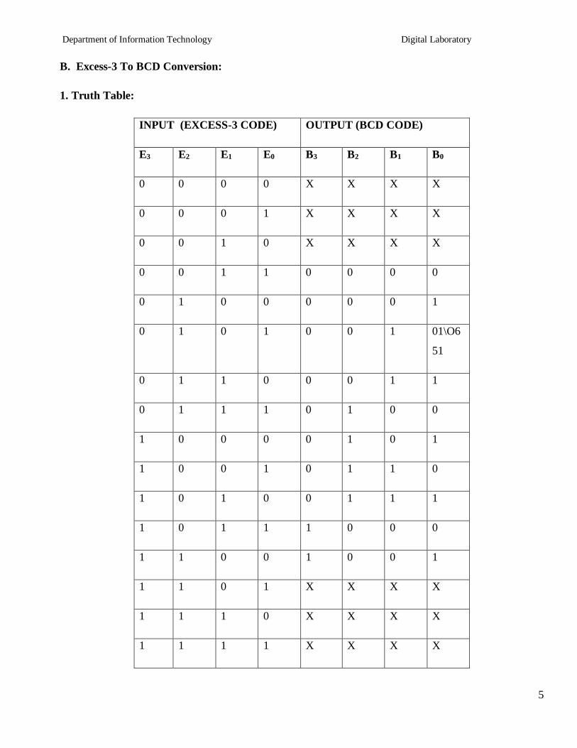
Department of Information Technology Digital Laboratory
5
B Excess-3 To BCD Conversion
1 Truth Table
INPUT (EXCESS-3 CODE) OUTPUT (BCD CODE)
E3 E2 E1 E0 B3 B2 B1 B0
0 0 0 0 X X X X
0 0 0 1 X X X X
0 0 1 0 X X X X
0 0 1 1 0 0 0 0
0 1 0 0 0 0 0 1
0 1 0 1 0 0 1 01O6
51
0 1 1 0 0 0 1 1
0 1 1 1 0 1 0 0
1 0 0 0 0 1 0 1
1 0 0 1 0 1 1 0
1 0 1 0 0 1 1 1
1 0 1 1 1 0 0 0
1 1 0 0 1 0 0 1
1 1 0 1 X X X X
1 1 1 0 X X X X
1 1 1 1 X X X X
Department of Information Technology Digital Laboratory
6
2) K-Map For Reduced Boolean Expressions Of Each Output
Fig 5 K-Map For Reduced Boolean Expressions Of Each Output (BCD Code)
Department of Information Technology Digital Laboratory
7
3) Circuit Diagram Test the circuit for all possible combinations of input and output codes
4) Hardware Requirements Table
Table 2 Hardware Requirement Table
GATE Quantity
IC Quantity
XOR 1 7486 1
NOT 3 7404 1
AND 8 7408 2
OR 3 7432 1
Pin Diagrams
Department of Information Technology Digital Laboratory
8
7400 Quad 2-Input NAND Gate
7402 Quad 2-Input NOR Gate
7404 Not Gates
7408 Quad 2-Input AND Gates
7432 Quad 2-Input OR Gate
7486 Quad 2-Input Exclusive-OR Gate
Department of Information Technology Digital Laboratory
9
Conclusion
Thus we studied different codes and their conversions including applications
The truth tables have been verified using IC 7486 7432 7408 and 7404
FAQrsquos with answers
Q1) What is the need of code converters
There is a wide variety of binary codes used in digital systems Often it is required to convert from one
code to another For example the input to a digital system may be in natural BCD and output may be 7-
segment LEDs The digital system used may be capable of processing the data in straight binary format
Therefore the data has to be converted from one type of code to another type for different purpose
Q2) What is Gray code
It is a modified binary code in which a decimal number is represented in binary form in such a way that
each Gray- Code number differs from the preceding and the succeeding number by a single bit
(eg for decimal number 5 the equivalent Gray code is 0111 and for 6 it is 0101 These two codes differ
by only one bit position i e third from the left) It is non weighted code
Q3) What is the significance of Gray code
Important feature of Gray code is it exhibits only a single bit change from one code word to the next in
sequence Whereas by using binary code there is a possibility of change of all bits if we move from one
number to other in sequence (eg binary code for 7 is 0111 and for 8 it is 1000) Therefore it is more
useful to use Gray code in some applications than binary code
Q4) What are applications of Gray code
1 Important feature of Gray code is it exhibits only a single bit change from one code word to the next in
sequence This property is important in many applications such as Shaft encoders where error
susceptibility increases with number of bit changes between adjacent numbers in sequence
2 It is sometimes convenient to use the Gray code to represent the digital data converted from the analog
data (Outputs of ADC)
3 Gray codes are used in angle-measuring devices in preference to straight forward binary encoding
Department of Information Technology Digital Laboratory
10
4 Gray codes are widely used in K-map
Q5) What are weighted codes and non-weighted codes
In weighted codes each digit position of number represents a specific weight The codes 8421 2421 and
5211 are weighted codes Non weighted codes are not assigned with any weight to each digit position ie
each digit position within the number is not assigned a fixed value Gray code Excess-3 code are non-
weighted code
Q6) Why is Excess-3 code called as self-complementing code
Excess-3 code is called self-complementing code because 9rsquos complement of a coded number can be
obtained by just complementing each bit
Q7) What is invalid BCD
With four bits sixteen numbers (0000 to 1111) can be represented but in BCD code only 10 of these are
used as decimal numbers have only 10 digits fro 0 to 9 The six code combinations (1010 to 1111) are not
used and are invalid
Department of Information Technology Digital Laboratory
11
Regularity Content Viva-voce Timely
Submission Total
Dated Sign of
Subject
Teacher
2 4 2 2 10
Date of Performance Date of Completion
-------------------------------------------------------------------------------------------------------------------
Assignment No 2
------------------------------------------------------------------------------------------------------------------
Title BCD amp Excess 3 Adder
------------------------------------------------------------------------------------------------------------------
Objective 1 To study the BCD arithmetic rules
2 Comparison between binary and BCD codes
Problem Statement Design (truth table K-map) and implementation of 4-bit BCD to Excess-3 and
Excess-3 to BCD Code converters
-----------------------------------------------------------------------------------------------------------------
Hardware Requirement
i) IC 7483 (4 bit Binary adder) IC 7404(Hex INV) 7432 (OR-gate) 7408 (AND-gate)
ii) 7486 (EX-OR gate)
iii) Digital Trainer Kit -1
iv) Patch cords
----------------------------------------------------------------------------------------------------------------
Software Requirement Digital Work 30
------------------------------------------------------------------------------------------------------------------
Theory
BCD-Binary coded decimal-In this code each decimal digit represent by a 4-bit binary no BCD is a
way to express each of the decimal digits with binary code Positional weights associated to the binary bits
in BCD code are (MSB) 8-4-2-1(LSB)
BCD number 0 to 9 but greater than 9 is invalid BCD
Department of Information Technology Digital Laboratory
12
So Convert in valid BCD using add 6 ie (0110)
BCD Adder
BCD adder is a circuit that adds two BCD digits amp produces a sum of digits also in BCD
Rules for BCD addition
1 Add two numbers using rules of Binary addition
2 If the 4 bit sum is greater than 9 or if carry is generated then the sum is invalid To correct the sum
add 0110 i e (6)10 to sum If carry is generated from this addition add it to next higher order BCD
digit
3 If the 4 bit sum is less than 9 or equal to 9 then sum is in proper form
CASE I Sum lt= 9 amp carry = 0
Add BCD digits 3 amp 4
1 0 0 1 1
+ 0 1 0 0
------------
0 1 1 1
Answer is valid BCD number = (7)BCDamp so 0110 is not added
CASE II Sum gt 9 amp carry = 0
Add BCD digits 6 amp 5
1 0 1 1 0
+ 0 1 0 1
-----------
10 1 1
Department of Information Technology Digital Laboratory
13
Invalid BCD (since sum gt 9) so 0110 is to be added
2 1 0 1 1
+ 0 1 1 0
-----------
1 0 0 0 1
(1 1)BCD
Valid BCD result = (11) BCD
CASE III Sum lt = 9 amp carry = 1
Add BCD digits 9 amp 9
1 1 0 0 1
+1 0 0 1
-----------
1 0 0 1 0
Invalid BCD ( since Carry = 1 ) so 0110 is to be added
2 1 0 0 1 0
+ 0 1 1 0
------------
1 1 0 0 0
(1 8)BCD
Valid BCD result = (18) BCD
Design of BCD adder
1 To execute first step i e binary addition of two 4 bit numbers we will use IC 7483
( withCin = 0 ) which is 4 bit binary adder
2 We need to design a digital circuit which will sense sum amp carry of IC 7483 amp if sum exceeds 9 or
carry = 1 this digital circuit will produce high output otherwise its output will be zero
Circuit to check invalid BCD
Department of Information Technology Digital Laboratory
14
First we will design circuit to check sum amp then we will logically OR output of this circuit to carry
output of IC 7483
For digital circuit which we are going to design we will have 4 inputs
( S3 S2 S1 S0) amp only 1 output Y
a) Y output of this circuit Will be ORed with carry output of first adder IC
7483
b) If BCD result is invalid i e sum output of first 7483 we have to add
(6)10 ie (0110)2 that means we need one more binary adder IC 7483
c) If BCD result is valid ( ie final output of the circuit to check validity is 0) we will make an
arrangement that second adder IC 7483 adds (0)10 i e ( 0000 )2 to the sum of the first adder IC 7483
The output of the combinational circuit is used as final output carry amp carry output of second adder IC is
ignored
i ) Truth Table for design of combinational circuit for BCD adder to check invalid
BCD
K-map for output- Y=S3S2+S3S1
Department of Information Technology Digital Laboratory
15
iii) Circuit diagram
v) Hardware Requirements
GATE Quantity
IC Quantity
Binary adder 2 7483 2
AND 2 7408 1
OR 2 7432 1
B ) Design and Implement single digit EXCESS-3 adder using IC 7483
Excess-3 code is a non weighted code It is a modified form of a BCD code The Excess-3 code can be
derived from the natural BCD code by adding 3 to each coded number It is also known as Self
Complementary code
Excess-3 code is a self complementary code because 1rsquos complement of Excess-3 number is Excess-3
code for the 9rsquos complement of corresponding number
Output of BCD adder
Department of Information Technology Digital Laboratory
16
Eg Excess-3 code for (4)10 is (0111)XS-3 1rsquos complement of this number is 1000 which is Excess-3 code
for (5)10and 5 is 9rsquos complement of (4)10
Rules for Excess-3 addition
i Add two Exceess-3 numbers
ii If carry is 1 add 3 to Sum
iii If carry is 0 subtract 3 from sum
Eg (8)10 + (6)10
(8)10 = 1011 (Excess-3 for 8)
(6)10= 1001 (Excess-3 for 6)
_______________
1 0100
0011 0011
_______________
0100 0111 ( Excess 3 code for (14)10
(i)Design
1) 4 bit Binary addition of excess 3 codes of two operands can be implemented with IC 7483
2) We have to design the circuit which will either add 0011 or subtract 0011 ie add 1101 (2rsquos
complement of 0011)depending upon carry bit
Letrsquos compare 0011 and 1101
B3 B2 B1 B0
0 0 1 1 ------- When carry is 1
1 1 0 1 ------- When carry is 0
Here B0 bit in both situation is High
Now compare B3 B2 and B1 It is complement of each other
When carry is 1 Bit B1 =1 B2=B3=0
When carry is 0 Bit B1 =0 B2=B3=1
B1 bit follows the carry and B2 and B3 bit complements the carry
(ii) Circuit Diagram
Department of Information Technology Digital Laboratory
17
(iii ) HARDWARE REQUIREMENTS
Sl No IC Description Quantity
1 7404 Not Gate 01
2 7483 4 bit Binary Adder 04
CONCLUSION
BCD adder ampsubtractor is designed amp tested for all possible combinations
FAQrsquos
1 Explain and Write the significance of BCD number system
2 Write the applications of BCD amp Excess 3 code
3 Explain the rules of BCD amp Excess 3 arithmetic
4 What is the difference between BCD and binary codes
5 What do you mean by unpacked and packed BCD nos
Department of Information Technology Digital Laboratory
18
Regularity Content Viva-voce Timely
Submission Total
Dated Sign of
Subject
Teacher
2 4 2 2 10
+
Date of Performance Date of Completion
-------------------------------------------------------------------------------------------------------------------
Assignment No 3
---------------------------------------------------------------------------------------------------------------------------
Title Implementation of logic functions
----------------------------------------------------------------------------------------------------------------------
Objective 1 To study the difference between multiplexer demultiplexer and decoder
2To study the applications of multiplexer
---------------------------------------------------------------------------------------------------------------------
Problem Statement Implement of Logic function using multiplexer IC 74153
---------------------------------------------------------------------------------------------------------------------
Hardware Requirement
i) IC 74153 74138 7404 7432
ii) Digital Trainer Kit -1
iii) Patch cords
----------------------------------------------------------------------------------------------------------------
Software Requirement Digital Work 30
------------------------------------------------------------------------------------------------------------------
Theory
D CWigital Multiplexer
Multiplexer are combinational digital circuits equating as controlled switches with several data inputs (I0
I1 I2 hellip) amp one single data output (ldquooutrdquo)At any time one of the Ip is transmitted to output According to
binary signals applied on control pairs to circuit Usually the number of data inputs is a power of two
Multiplexing is the process of transmitting a large no of information units over a small no of channel
digital multiplexer is a combinational large circuit which performs the operation of multiplexing It selects
Department of Information Technology Digital Laboratory
19
the operation of multiplexing It selects the operation of binary information from one of the many input
lines amp transfer to a single op line Multiplexer is called a data selector or multiposition switch because it
selects one of the many input Selection of a particular line is controlled by a set of a selection lines or
selects inputs The number of select lines depends upon no of input lines Generally there
is lsquonrsquo selects line for lsquomrsquo input lines By applying a particular code on select lines is transmitted on the
output linesBlock diagram of MUX is shown at contains lsquo2mrsquo input lines lsquomrsquo select Such that 2m = n amp
one unable input which is used to activate or dedicate MUX Depending upon the no of IP amp OP lines
various types of multiplexers are available We have 21 41 81 161 MUX Here the first no indicates
the no of input lines amp second no indicates the no of output lines
E is called as enable input which is generally active low
Fig-Block diagram for N1 Multiplxer
Demultiplexer
Demultiplexer is a logic used to perform exactly reverse function performed by multiplexer It accepts a
single input and distributes among several outputs The selection of a particular output line is controlled
by a set of selection line There are n input lines amp 2m is the number of selection line whose bit
combinations determine which output to be selected
Encoder amp Decoder
1 Encoders are used to encode given digital number into different numbering format like
decimal to BCD Encoder Octal to Binary
2 Decoders are used to decode a coded binary word like BCD to seven segment decoder
3 Thus encoder and decoder are application specific logic develop we can not use any type of
input for any encoder and decoder
Smhelliphellips1 s0
Output(Y)
D0
D1
D2
D3
Dn
N1
multiplxer
E
Department of Information Technology Digital Laboratory
20
4 Need to select input according to encoder and decoder being selected for a particular
application as mention in examples above
Uses of Mux
1 Use for Boolean function implementation
2 Construct a common bus system
3 To select between multiple sources amp signal destination
4 Inter register transfer
Advantages
1) Simplification of logic expression not required
2) Logic design is simplified
Disadvantage
Only one function can be implemented using one MUX Hence they canrsquot be used in
combinational logic circuit which contains many function
Part-A (IC 74153)
1 VERIFICATION OF IC 74153
IC 74153 is a dual layer 41 MUX It has four input lines for (I0D-I3D) for second MUX amp active high
output lsquoYarsquo lsquoYbrsquo (1Y or 2Y) It has select lines S1S0 common to both MUX The Enable inputs are
active low EaampEb(1G and 2G) The MUX is activated when they are at logic o
Pin out of IC 74153
Department of Information Technology Digital Laboratory
21
Function table of IC 74153 (X= Donrsquot Care Condition)
Select Input
Inputs (I or II) Output
S1 S0 E (I or II) D0 D1 D2 D3 Y
X X 1 X X X X 0
0 0 0 0 X X X 0
0 0 0 1 X X X 1
0 1 0 X 0 X X 0
0 1 0 X 1 X X 1
1 0 0 X X 0 X 0
1 0 0 X X 1 X 1
1 1 0 X X X 0 0
1 1 0 X X X 1 1
2CASCADING OF IC 74153
Cascading is done to expand two or more MUX ICrsquos to a digital multiplexer with larger no of inputs ie
multiplexer stocks or tress is designed The enable input is used for cascading In case of IC 74153 we
have only two select lines But for certain application 3 select lines are required then it can be
obtained by cascading using enable Now with 3 select lines we have 8 combinations Out of this
combination the MSB is O MSB is 1 for last four combination so we can use these MSB to select
any 1 MUX out of two by connecting it to E pin of first 41 MUX
Function table of IC 74153 as 8 1 Mux by cascading 2 41 Mux
Select Input Output
C (1G 2G ) B (S1) A (S0) Y
0 0 0 D0
0 0 1 D1
0 1 0 D2
0 1 1 D3
1 0 0 D4
1 0 1 D5
Department of Information Technology Digital Laboratory
22
1 1 0 D6
1 1 1 D7
3FUNCTION IMPLEMENTATION
Y= sum m (1 3 5 6)
Thisexpression is in Standard SOP form and it is three variable function So we need to use mux with
three select inputs ie 81 Mux Already we have implemented 81 Mux using IC 74153 For Boolean
function in Standard SOP form we connect data inputs corresponding to the minterms present in the given
function to Vcc and remaining data inputs to ground
Truth table
Inputs Output
C B A Y
0 0 0 0
0 0 1 1
0 1 0 0
0 1 1 1
1 0 0 0
1 0 1 1
1 1 0 1
1 1 1 0
LOGIC DIAGRAM
Hardware Requirements
GATE Quantity
IC Quantity
Mux 1 74153 1
NOT 1 7404 1
OR 1 7432 1
Department of Information Technology Digital Laboratory
23
Part-B Decoder (IC 74138)
Theory
Discrete quantities of information are requested in digital system with binary codes A binary code of n
bits is capable of representing into 2n distinct elements of the coded information
Decoder converts coded input to coded outputs accepts one of the code
There are different types of decoders such as 38 decoder 416 line decoders etc These are in general
called as n m line decoder where m=2n and n= no of input lines and m=no of output lines Demux also
takes one input data line source and selectively distributes it to one of n output channels The only
difference between demux and decoder is that demux has Din (data ip) line whereas decoder does not
have
ADVANTAGES
1) The decoder provides best implementation whenever there are many outputs of the combinational
circuit and each op of the function (or its complement) is required to be expressed with a small no
of minterms
2) The decoder can function as demux If the Enable ip line is taken as Din (data ip)
DISADVANTAGES
Since decoder method requires an OR gate for each op function so there is new hardware used And it is
always advisable to use minimum hardware as we come across problems like propagation delay of gates
APPLICATIONS
Decoder is worthily used for decoding binary information and memory interfacing It is used for the
implementation of Boolean function
Differentiate between Mux Demux Decoder
Point Multiplexer Demultiplexer Decoder
Input Many input lines Single input line Many input line also Acts as select line
Output Single output line Many output line Many output lineActive low output
Select line 2m = n n = 2m Enable inputs used
Department of Information Technology Digital Laboratory
24
A) Verification of IC 74138
We use IC 74138 which accepts 3 binary weighted inputs (A0 A1 A2) and when enabled provides
mutually exclusive active low outputs (y0-y7) It features 3 Enable ips Two active low (G2A G2B) and
one active high (G1) Every output will be high unless G2A G2Bare low and G1 is high It has
demultiplexing capability and multiple enable ips for easy expansion
IC Diagram
Function Table of 38 decoder
Input Output
Enable Data
G2A G2B G1 A2 A1 A0 Y0 Y1 Y2 Y3 Y4 Y5 Y6 Y7
0 0 0 X X X 1 1 1 1 1 1 1 1
0 1 1 X X X 1 1 1 1 1 1 1 1
1 0 1 X X X 1 1 1 1 1 1 1 1
1 1 1 X X X 1 1 1 1 1 1 1 1
Department of Information Technology Digital Laboratory
25
0 0 1 0 0 0 0 1 1 1 1 1 1 1
0 0 1 0 0 1 1 0 1 1 1 1 1 1
0 0 1 0 1 0 1 1 0 1 1 1 1 1
0 0 1 0 1 1 1 1 1 0 1 1 1 1
0 0 1 1 0 0 1 1 1 1 0 1 1 1
0 0 1 1 0 1 1 1 1 1 1 0 1 1
0 0 1 1 1 0 1 1 1 1 1 1 0 1
0 0 1 1 1 1 1 1 1 1 1 1 1 0
B) Cascading of IC 74138
The enable ip G1 active high of IC 74138 is used for cascadingfor cascading 2 ICrsquos the enable ip G1 of
first IC is connected to G1 enable ip of second IC through a NOT gate This enable ip is used as MSB
select ip line A3 the other three select input lines of both ICrsquos (A0A1A2) are also shorted to select
input lines of second IC to get single ip select lines (A0A1A2)
The ip line A3 is used to enable disable the 2 IC 74138 decoders When A3=0 first IC is enabled and
second is disabled Thus the first decoder will generate minterms from 0000 to 0111 as op and the second
decoder will generate nothing When A3=1 the enable conditions are reversed and thus second decoder
IC will generate minterms 1000 to 1111
Function Table of 416 decoder using IC 74138 (38 decoder)
Input Output
Enable Data
G2
A
G2
B
A
3
A
2
A
1
A
0
Y
0
Y
1
Y
2
Y
3
Y
4
Y
5
Y
6
Y
7
Y
8
Y
9
Y1
0
Y1
1
Y1
2
Y1
3
Y1
4
Y1
5
0 1 X X X X 1 1 1 1 1 1 1 1 1 1 1 1 1 1 1 1
Department of Information Technology Digital Laboratory
26
1 0 X X X X 1 1 1 1 1 1 1 1 1 1 1 1 1 1 1 1
1 1 X X X X 1 1 1 1 1 1 1 1 1 1 1 1 1 1 1 1
0 0 0 0 0 0 0 1 1 1 1 1 1 1 1 1 1 1 1 1 1 1
0 0 0 0 0 1 1 0 1 1 1 1 1 1 1 1 1 1 1 1 1 1
0 0 0 0 1 0 1 1 0 1 1 1 1 1 1 1 1 1 1 1 1 1
0 0 0 0 1 1 1 1 1 0 1 1 1 1 1 1 1 1 1 1 1 1
0 0 0 1 0 0 1 1 1 1 0 1 1 1 1 1 1 1 1 1 1 1
0 0 0 1 0 1 1 1 1 1 1 0 1 1 1 1 1 1 1 1 1 1
0 0 0 1 1 0 1 1 1 1 1 1 0 1 1 1 1 1 1 1 1 1
0 0 0 1 1 1 1 1 1 1 1 1 1 0 1 1 1 1 1 1 1 1
0 0 1 0 0 0 1 1 1 1 1 1 1 1 0 1 1 1 1 1 1 1
0 0 1 0 0 1 1 1 1 1 1 1 1 1 1 0 1 1 1 1 1 1
0 0 1 0 1 0 1 1 1 1 1 1 1 1 1 1 0 1 1 1 1 1
0 0 1 0 1 1 1 1 1 1 1 1 1 1 1 1 1 0 1 1 1 1
0 0 1 1 0 0 1 1 1 1 1 1 1 1 1 1 1 1 0 1 1 1
0 0 1 1 0 1 1 1 1 1 1 1 1 1 1 1 1 1 1 0 1 1
0 0 1 1 1 0 1 1 1 1 1 1 1 1 1 1 1 1 1 1 0 1
0 0 1 1 1 1 1 1 1 1 1 1 1 1 1 1 1 1 1 1 1 0
C) Implementation of Boolean function
The procedure for implementation of combinational circuit by means of a decoder and lsquoORrsquo gates requires
that the Boolean function fir the circuit be expressed in Sum of Minterms These forms can be obtained by
Department of Information Technology Digital Laboratory
27
expanding the function A decoder is then chosen which generates all the minterms of n ip variables The
ip to each OR gate are selected from the decoder outputs according to the minterms list in each function
i) F1=summ (1 3 5 7)
Truth table
Logic Diagram
ii) F2=summ (1 3 5 7111315)
Truth table
Logic Diagram
Conclusion In this way multiplexer Decoderamp its applications are studied implemented amp
tested
FAQrsquos
1What is a multiplexer
2What is a Demultiplexer
3 Enlist applications of multiplexer
Department of Information Technology Digital Laboratory
28
Regularity Content Viva-voce Timely
Submission Total
Dated Sign of
Subject
Teacher
2 4 2 2 10
Date of Performance Date of Completion
-------------------------------------------------------------------------------------------------------------------
Assignment No4
------------------------------------------------------------------------------------------------------------------
Title 3 bit updown Asynchronous and Synchronous counter using IC7476
------------------------------------------------------------------------------------------------------------------
Objective To understand design procedure of asynchronousamp Synchronous counter
------------------------------------------------------------------------------------------------------------------
Problem Statement Design (State diagram state table amp K map) and implementation of 3
bit Up and Down Asynchronous and Synchronous Counter using master slave JK flip-flop IC 7476
-----------------------------------------------------------------------------------------------------------------
Hardware Requirement
i) IC 7476 (MS-JK Flip-flop) IC 7408(Quad 2 ip AND Gate)
IC 7432 (Quad 2 ip OR Gate) and IC 7404 (Hex Inverter)
ii) Digital Trainer Kit -132
iii) Patch cords
----------------------------------------------------------------------------------------------------------------
Software Requirement Digital Work 30
------------------------------------------------------------------------------------------------------------------
Theory
Counters counters are logical device or registers capable of counting the no of states or no of clock
pulses arriving at its clock input where clock is a timing parameter arriving at regular intervals of time
so counters can be also used to measure time amp frequencies They are made up of flip flops Where the
Department of Information Technology Digital Laboratory
29
pulse are counted to be made of it goes up step by step amp the op of counter in the flip flop is decoded to
read the count to its starting step after counting n pulse incase of module counters
Types of Counters
Counter are of two types
1) Asynchronous counter
2) Synchronous counter
Asynchronous counter
A digital counter is a set of flip flop The flip flop are connected such that their combined state at any time
is binary equivalent of total no of pulses that have occurred up to that time Thus its name implies a
counter is used to count pulse A counter is used as frequency dividers To obtain waveform with
frequency that is specific fraction of clock frequency
Counter may be Asynchronous or synchronous The Asynchronous counter is also called as ripple counter
An Asynchronous counter uses T flip flop to perform a counting function The actual hardware used is
usually J-K flip flop with J amp K connected to logic1Even D flip flops may be used here
In asynchronous counter commonly called ripple counter the first flip-flop is clocked by the external
clock pulse amp then each successive flip-flop is clocked by the Q or Qrsquo output of the previous flip-flop
Therefore in an asynchronous counter the flip-floprsquos are not clocked simultaneously The input of MS-JK
is connected to VCC because when both inputs are one output is toggled As MS-JK is negative edge
triggered at each high to low transition the next flip-flop is triggered
Synchronous Counter
When counter is clocked such that each flip flop in the counter is
triggered at the same time the counter is called as synchronous counter
The gates propagation delay at reset time will not be present or we may say will not occur
1) Asynchronous Up Counter
Fig 1 shows 3bit Asynchronous Up Counter Here Flip-flop 2 act as a MSB Flip-flop and Flip-flop 0 act
as a LSB Flip-flop Clock pulse is connected to the Clock of Flip-flop 0 Output of Flip-flop 0(Q0) is
connected to clock of next flip-flop (ie Flip-flop 1) and so on As soon as clock pulse changes output is
going to change (at the negative edge of clock pulse) as a Up count sequence For 3 bit Up counter state
table is as shown below
Department of Information Technology Digital Laboratory
30
State Table
Logic diagram
Fig 1 3 Bit Asynchronous Up Counter
Hardware requirements
Gate
Flip flop
Quantity IC Quantity
MS JK 3 7476 2
2) Down Counter
Fig 2 shows 2 bit Asynchronous Down Counter Here Flip-flop 2 act as a MSB Flip-flop and Flip-flop 0
act as a LSB Flip-flop Clock pulse is connected to the Clock of Flip-flop 0 Output of Flip-flop 0 (Q0rsquo) is
Counter States Count
Q2 Q1 Q0
0 0 0 0
1 0 0 1
2 0 1 0
3 0 1 1
4 1 0 0
5 1 0 1
6 1 1 0
7 1 1 1
8 0 0 0
Department of Information Technology Digital Laboratory
31
connected to clock of next flip-flop (ie Flip-flop 1) and so on As soon as clock pulse changes output is
going to change (at the negative edge of clock pulse) as a down count sequence For 3 bit down counter
sate table is as shown below
In both the counters Inputs J and K are connected to Vcc hence J-K Flip flop work in toggle mode Preset
and Clear both are connected to logic 1
State Table
Logic diagram
Fig 2 3 Bit Asynchronous Down Counter
Hardware requirements
Counter States Count
Q2 Q1 Q0
7 1 1 1
6 1 1 0
5 1 0 1
4 1 0 0
3 0 1 1
2 0 1 0
1 0 0 1
0 0 0 0
7 1 1 1
Department of Information Technology Digital Laboratory
32
Gate
Flip flop
Quantity IC Quantity
MS JK 3 7476 2
Applications
The asynchronous counters are specially used as the counting devices
They are also used to count number of pulses applied
It also works as frequency divider
It helps in counting the number of product coming out of the machinery where product is coming out at
equal interval of time
Types of synchronous counter
1) Up counter
2) Down counter
1 3 bit Synchronous up counter
The up counter counts from 0 to7 ie(000 to 111)for this we are using MS JK flip flop In IC 74LS76 2
MS J-K flip flops are present The clock pulse is given at pin 1 amp 6 of the 1st IC amp pin 1 of 2nd IC Next
state decoder logic is designed with the help of state table
State table for synchronous up counter
Present state Next state Flip flop 3 Flip flop 2 flip flop 1
Q2 Q1 Q0 Q2 Q2 Q0 J2 K2 J1 K1 J0 K0
0 0 0 0 0 1 0 x 0 X 1 x
0 0 1 0 1 0 0 x 1 X x 1
0 1 0 0 1 1 0 x x 0 1 x
0 1 1 1 0 0 1 x x 1 x 1
1 0 0 1 0 1 x 0 0 X 1 X
1 0 1 1 1 0 x 0 1 X x 1
1 1 0 1 1 1 x 0 x 0 1 X
1 1 1 0 0 0 x 1 x 1 x 1
Department of Information Technology Digital Laboratory
33
K-Map
Q1Q0
Q2
00 01 11 10
0 0 0 1 0
1 X X X X
J2= Q1Q0
Q1Q0
Q2
00 01 11 10
0 X X X X
1 0 0 1 0
K2= Q1Q0
Q1Q0
Q2
00 01 11 10
0 0 1 X X
1 0 1 X X
J1= Q0
Q1Q0
Q2
00 01 11 10
0 X X 1 0
1 X X 1 0
K1= Q0
Department of Information Technology Digital Laboratory
34
Q1Q0
Q2
00 01 11 10
0 1 X X 1
1 1 X X 1
J0= 1
Q1Q0
Q2
00 01 11 10
0 X 1 1 X
1 X 1 1 X
K0= 1
Logic Diagram
Fig 1 3 bit Synchronous up counter
Department of Information Technology Digital Laboratory
35
2 3 bit Synchronous down counter
This is used to count from 7-0 ie(111-000)for this also 2 ICrsquos of 74LS76 are required amp hence we use 3
MS JK flip flops Here also clock is given to 1stamp 6th pin of 1st IC amp1st pin of 2nd IC enabling to apply
clock to all flip flop at a time Next state decoder logic is designed with the help of state table
State table for synchronous down counter
Present state Next state Flip flop 3 Flip flop 2 Flip flop 1
Q2 Q1 Q0 Q2 Q1 Q0 J2 K2 J1 K1 J0 K0
1 1 1 1 1 0 X 0 X 0 X 1
1 1 0 1 0 1 X 0 X 1 1 X
1 0 1 1 0 0 X 0 0 X X 1
1 0 0 0 1 1 X 1 1 X 1 X
0 1 1 0 1 0 0 X X 0 X 1
0 1 0 0 0 1 0 X X 1 1 X
0 0 1 0 0 0 0 X 0 X X 1
0 0 0 1 1 1 1 X 1 X 1 X
K-Map
Q1Q0
Q2
00 01 11 10
0 1 0 0 0
1 X X X X
J2= Q1Q0
Q1Q0
Q2
00 01 11 10
Department of Information Technology Digital Laboratory
36
0 X X X X
1 1 0 0 0
K2= Q1Q0
Q1Q0
Q2
00 01 11 10
0 1 0 X X
1 1 0 X X
J1= Q0
Q1Q0
Q2
00 01 11 10
0 X X 0 1
1 X X 0 1
K1= Q0
Q1Q0
Q2
00 01 11 10
0 1 X X 1
1 1 X X 1
J0= 1
Q1Q0
Q2
00 01 11 10
0 X 1 1 X
1 X 1 1 X
K0= 1
Department of Information Technology Digital Laboratory
37
Logic Diagram
Fig 2 3 bit Synchronous down counter
Uses
1 Specially used as the counting devices
2 Used in frequency divider circuit
3 Used in digital voltmeter
4 Used in counter type A to D converter
5 Used for time measurement
6 It helps in counting the no of product coming out from machinery where product is coming out
at equal interval of time
Conclusion
Up and down counters are successfully implemented the counters are studied amp op are checked The
state table is verified
PRACTICE ASSIGNMENTS EXERCISE MODIFICATIONS
1 Design amp implement 2 bit controlled synchronous counter
2 Designamp implement 4 bit controlled synchronous counter
3 Designamp implement truncated synchronous up or down counter
FAQrsquos with answers
1 What do you mean by Counter
A Counter is a register capable of counting the no of clock pulses arriving at its
clock inputs Count represents the no of clock pulses arrived A specified
sequence of states appears as the counter output
Department of Information Technology Digital Laboratory
38
2 What are the types of Counters Explain each
There are two types of counters as Asynchronous Counter and Synchronous Counter
Asynchronous Counter In this counter the first flip-flop is clocked by the external clock pulse
and then each successive flip-flop is clocked by the Q or Qrsquo op of the previous flip-flop Hence in
Asynchronous Counter flip-flops are not clocked simultaneously and hence called as Ripple
Counter Synchronous Counter In this counter the common clock input is connected to all the
flip-flops simultaneously
3 What do you mean by pre-settable counters
A counter in which starting state is not zero can be designed by making use of the
preset inputs of the flip flops This is referred to as loading the counter
asynchronously This is referred to as pre-settable counter
4 What are the applications of synchronous counters
Digital clock
Frequency divider circuits
Frequency counters
Used in analog to digital converters
5 What are the advantages of synchronous counters over asynchronous counters
Propagation delay time is reduced
Can operate at a much higher frequency than the asynchronous counters
6 Ring counter is an example of synchronous counters or asynchronous counter
Synchronous counter Since all the flip flops are clocked simultaneously
7 Twisted Ring (Johnsonrsquos) counter is an example of synchronous counters or asynchronous
counter
Synchronous counter Since all the flip flops are clocked simultaneously
8 What is the difference between ring counter and twisted ring counter
In ring counter pulses to be counted are applied to a counter it goes from state to state and the
output of the flip flop s in the counter is decoded to read the count Here the uncomplimentary
output (Q) of last flip flop is fed back as an input to first flip flop Ring counters are referred as
MOD lsquoNrsquo counters
Department of Information Technology Digital Laboratory
39
But in Twisted ring counter the complimentary output (Q bar) of last flip flop is fed back as an
input to first flip flop Twisted Ring counters are referred as MOD lsquo2Nrsquo counters
9 What are the applications of ring counters
Ring counter outputs are sequential non-overlapping pulses which are useful for control state
counters Used in stepper motor this requires pulses to rotate it from one position to the next Used
as divide by lsquoNrsquo ((MOD lsquoNrsquo) counters
10 What are the applications of ring counter twisted ring counters
Used as divide by lsquo2Nrsquo ((MOD lsquo2Nrsquo) counters
Used for control state counters
Used for generation of multiphase clock
11 List the Synchronous Counter ICs
IC 74160 Decade Up Counter
IC 74161 4 bit binary Up Counter
IC 74162 Decade Up Counter
IC 74163 4 bit binary Up Counter
IC 74168 Decade UpDown Counter
IC 74169 4 bit Binary UpDown Counter
IC 74190 Decade UpDown Counter
IC 74191 4 bit Binary UpDown Counter
IC 74192 Decade UpDown Counter
IC 74193 4 bit Binary UpDown Counter
Department of Information Technology Digital Laboratory
40
Regularity Content Viva-voce Timely
Submission Total
Dated Sign of
Subject
Teacher
2 4 2 2 10
Date of Performance Date of Completion
-------------------------------------------------------------------------------------------------------------------
Assignment No 5
-------------------------------------------------------------------------------------------------------------------------------
Title Design and implementation of Module lsquonrsquo counter with IC7490 and IC 74191
-----------------------------------------------------------------------------------------------------------------------------
Objective To know difference between regular amp truncated counter as well as binary ampBCD Counter
--------------------------------------------------------------------------------------------------------------------------------
Problem Statement To design and implement mod - 10 mod ndash 7 mod - 99 asynchronous BCD
counter using IC 7490 and to design and implement up down mod - n Binary counter using IC 74191
-----------------------------------------------------------------------------------------------------------------
Hardware Requirement
i) IC 7490 IC 74191 basic gates
ii) Digital Trainer Kit -1
iii) Patch cords
----------------------------------------------------------------------------------------------------------------
Software Requirement Digital Work 30
------------------------------------------------------------------------------------------------------------------
Theory
Part A ndash IC 7490
IC 7490 is a TTL MSI (medium scale integration) decade counter It contains 4 master slave flip flops
internally connected to provide MOD-2 ie divide by 2 and MOD-5 ie divide by 5 counters MOD-2 and
Mod-5 counters can be used independently or in cascading
Department of Information Technology Digital Laboratory
41
It is a 4-bit ripple type decade counter The device consists of 4-master slave flip flops internally
connected to provide a divide by two and divide by 5 sections Each section has a separate clock ip to
initiate state changes of the counter on the high to low clock transition
Since the op from the divide by 2 section is not internally connected to the succeeding stages The device
may be operated in various counting modes In a BCD counter the CP1 input must be externally connected
to QA op The CP0ip receives the incoming count producing a BCD count sequence It is also provided
with additional gating to provide a divide by 2 counter and binary counter for which the count cycle length
is divide by 5 The device may be operated in various counting modes
There are 2 reset inputs R0(1) and R0(2) both of which need to be connected to the lsquologic 1rsquo for clearing all
flip flops Two set inputs Rg(1) and Rg(2) when connected to logic 1 are used for setting counter to 1001
(BCD 9)
Pin out of IC 7490
Fig Pin configuration of IC7490
Table 1-pin name and description of IC7490
Pin name Description
Input B This is clock input to the internal MOD-5 ripple counter which is negative
edge triggered
R0(1)R0(2) Gated zero reset inputs
Department of Information Technology Digital Laboratory
42
R9(1)R9(2) These are gated set to nine inputs
QDQCQB Output of internal MOD-5 counter with QD as MSB
QA Output of internal MOD-2 counter with QA as LSB
Input A Clock input to FF-A which is negative edge triggered
Functional Table for IC7490
Reset inputs Output
R0(1) R0(2) R9(0) R9(1) QD QC QB QA
1 1 0 X 0 0 0 0
1 1 X 0 0 0 0 0
X X 1 1 1 0 0 1
X 0 X 0 COUNTER
0 X 0 X COUNTER
0 X X 0 COUNTER
X 0 0 x COUNTER
Department of Information Technology Digital Laboratory
43
Basic internal Structure of IC 7490
Function Table of MOD-5 counter
Design of MOD-10 counter using IC 7490
The QA op the first flip flop is connected to the input B which is clock ip of internal MOD-5 ripple
counter Due to cascading of Mod-2 and Mod-5 counters the overall configuration the decade counters
count from 0000 to 1001 After 1001 mod-5 resets to 0000 and next count after 1001 is 0000
When QA op is connected to B ip we have the Mod-2 counter followed by Mod-5 counter The
count sequence obtained is shown in the table It may be noted that QA changes from 0 to 1 the state of
InputB clock Output
Count QD QC QB
0 0 0 0
0 0 1 1
0 1 0 2
0 1 1 3
1 0 0 4
Department of Information Technology Digital Laboratory
44
Mod-5 counter doesnrsquot change whereas when QA changes from 1 to 0 the Mod-5 counter goes to the next
state
Logic DiagramMOD-10 counter using IC 7490
5 Modulus n Counter
Function table
Ip clock
Output
Count QD QC QB QA
0 0 0 0 0
0 0 0 1 1
0 0 1 0 2
0 0 1 1 3
0 1 0 0 4
Department of Information Technology Digital Laboratory
45
Design of Mod-7 Counter using IC 7490
Mod-7 counter counts through seven states from 0 to 6 counters and it should reset as soon as the
count becomes 7 The op of reset logic should be 1 corresponding to invalid states The reset logic op
should be applied to pin 2 and 3
Truth Table of Reset Logic
0 1 0 1 5
0 1 1 0 6
0 1 1 1 7
1 0 0 0 8
1 0 0 1 9
QD QC QB QA Y
0 0 0 0 0
0 0 0 1 0
0 0 1 0 0
0 0 1 1 0
0 1 0 0 0
0 1 0 1 0
0 1 1 0 0
0 1 1 1 1
1 0 0 0 1
1 0 0 1 1
Department of Information Technology Digital Laboratory
46
Logic Diagram Mod 7 Counter using IC 7490
Function table
Ip clock
Output
Count QD QC QB QA
0 0 0 0 0
0 0 0 1 1
0 0 1 0 2
0 0 1 1 3
0 1 0 0 4
0 1 0 1 5
0 1 1 0 6
Department of Information Technology Digital Laboratory
47
Design of Mod-99 using IC 7490
For Mod-99 two IC 7490rsquos will be required Hence to implement a divide by 99 counter we have
to use two decade counters ICrsquos A divide by 99 counter counts 99 states from 0 to 98 and the counter
should reset as soon as the count becomes 99 So in order to reset the counter of 99 connect the Q op
which are equal to 1 in the count of 99 to an lsquoAndrsquo gate amp then connect and op to the reset ip of both
ICrsquos
MOD-100 Counter-
MOD-100 counter can be obtained by cascading two decade counter ICrsquos
Each IC gives divide by 10 counts Hence 2 ICs will give 1010=100 counts
Clock is applied to the input A of IC 7490 the Q1 output is connected to B input etc
For cascading the QD output of the first IC is connected to the input A of second IC Thus QD of
IC-(1) acts as clock input to IC-(2)
The Ro (1) Ro(2) R9(1) R9(2) inputs of both ICs are connected to ground so as to make them
inactive
The total count provided by the two counters varies from 00 to 99 decimal that means 100 states
Hence it is a MOD-10 counter
Impleacutementations
FigureMOD-100 counters using IC 7490
Department of Information Technology Digital Laboratory
48
B) IC 74191 ndash Theory
IC74191 is 4-bit binary synchronous reversible up down counter It contains 4 master slave flip flops
with internal gating and steering logic to provide asynchronous reset and synchronous count updown
operations its asynchronous parallel capability permits the counter to be preset to any desire number D0
to D3 are the parallel data inputs Information present on the parallel data inputs D0 to D3 is loaded into
the counter and appears on the output when the load PLinput is lowThisoperation overrides the counting
function Counting is inhabited by the high level on the enable G input when G input is low internal state
changes are initiated synchronously by the low to high transitions of the clock inputs the updown input
signal determines the direction of input
Function Table
Operating
mode
Inputs Outputs
PL UD G CLK Dn
Parallel
load L X X X L L
L X X X H H
Count up H L 0 uarr X Count up
Count
down H H 0 uarr X
Count
down
Hold(No
change) H X H X X No change
Pin details ndash
D0 to D3 input lines PL parallel load
G is Enable input ndash enabling the counting
Q0 to Q3 output lines
Downup determines the direction of counting
Clk clock input for counter
Terminal Count Max(1111) min(0000) For these states signal goes high for 1clock pulse
Ripple clock Clock input for next higher state
Department of Information Technology Digital Laboratory
49
Pin Diagram IC 74191
Up counter- Truth Table
Clk
Pulses QA QB QC QD
0 0 0 0 0
1 0 0 0 1
2 0 0 1 0
3 0 0 1 1
4 0 1 0 0
5 0 1 0 1
6 0 1 1 0
7 1 1 1 1
8 1 0 0 0
9 1 0 0 1
10 1 0 1 0
11 1 0 1 1
12 1 1 0 0
13 1 1 0 1
Department of Information Technology Digital Laboratory
50
14 1 1 1 0
15 1 1 1 1
Logic Diagram
Steps-
Connect the circuit as shown above
Apply clock ip to pin no14
Connect UD to GND
Verify the output according to truth table
Logic diagram of down counter
Steps-
Connect the circuit as shown above
Apply clock ip to pin no14
Connect UD to VCC
Verify the output according to truth table
UD D3 D2 D1 D0 PL
Clock IC 74191
G RC
MAX MIN
Q3 Q2 Q1 Q0 TC
vcc
NC
NC
Outputs
no connection
vcc
Department of Information Technology Digital Laboratory
51
With the help of IC74191 we can implement truncated updown counter by using following logic ndash
Connect data input line to particular count you want to load
According to requirement make Truth table
Draw the K-map
Find out Boolean expression
Draw the logic diagram and that is the combinational logic for your count and apply the output of
that circuit to PL
According to requirement we get the UP and down counting
5 Modulus n Counter
Presettable updown counter
Mod 11 counter
Implementation of presetttable mod updown counter using IC- 74LS191
1 Load Data on data lines D0 to D3 (0101)
2 Counter will go through the states from 0101 0110hellip1111 in up counter and 0101 to 0000 in
down counter
Combinational Circuit
CLOCK D3 D2 D1 D0
TC
U D 74191 RC
G PL
Updown Q3 Q2 Q1 Q0 PL
Q3 Q2 Q1 Q0
Preset Count
Department of Information Technology Digital Laboratory
52
3 The logic circuit should be designed in such a way that only when all the outputs are high output
of the reset circuit should be low and the counter should jump to state 5 It should again start
counting from 0101 to 0000
State Table
Down Counter UP Counter
IC 74191 is 4 bit counter Thus it counts 0000 to 1111 different 16 states For MOD11 counter we require
different 11 states so 5 steps must be skipped from 16 states We get MOD11 by presetting counter to
value 5
Assignment Question
Design and Implement MOD 7 MOD 10 and MOD 12 using IC 74191
FAQs
1 What do you mean modulus counter
Counter
state Clock
pulse
Q3 Q2 Q1 Q0
1 0 1 0 1
2 0 1 1 0
3 0 1 1 1
4 1 0 0 0
5 1 0 0 1
6 1 0 1 0
7 1 0 1 1
8 1 1 0 0
9 1 1 0 1
10 1 1 1 1
11 1 1 1 1
Counter state
Clock pulse
FF outputs
Q3 Q2 Q1 Q0
1 0 1 0 1
2 0 1 0 0
3 0 0 1 1
4 0 0 1 0
5 0 0 0 1
6 0 0 0 0
7 0 1 0 1
Department of Information Technology Digital Laboratory
53
It represents the number of possible states of counter
2 How will you use the 7490 IC to design symmetrical divide by 10 frequency counter
The divide by 5 circuit followed by divide by 2 circuit will give symmetrical output
3Where counters are used Give real life example of counter
Modulus n Counter
Binary counter ndash An N stage counter that recycles after 2 Ncount The count proceds in specified binary
sequence Counter Presetable- A counter which can be set to a desired value before the start of the
counting UPDown counter ndash A counter that can count in both up and down direction depending upon a
control input
Department of Information Technology Digital Laboratory
54
Regularity Content Viva-voce Timely
Submission Total
Dated Sign of
Subject
Teacher
2 4 2 2 10
Date of Performance Date of Completion
-------------------------------------------------------------------------------------------------------------------
Assignment No6
------------------------------------------------------------------------------------------------------------------
Title Sequence Generator
------------------------------------------------------------------------------------------------------------------
Objective To understand sequence generator one of the sequential circuit
-------------------------------------------------------------------------------------------------------------------
Problem Statement Design (State Diagram State Table K Map) and implementation of Sequence
Generator using Shift Register IC 74194
-----------------------------------------------------------------------------------------------------------------
Hardware Requirement
i) IC 741947408 (AND-gate) 7432 (OR-gate)
ii) Digital Trainer Kit -1
iii) Patch cords
----------------------------------------------------------------------------------------------------------------
Software Requirement Digital Work 30
------------------------------------------------------------------------------------------------------------------
Theory
Part A Sequence Generator with Flip flop
A sequential circuit which generates a prescribed sequence of bits in synchronism with a clock is referred
to as a sequence generator These pulse trains or sequence of bits can be used to open valves close gates
turn on lights and turn off machines and other variety of jobs
Department of Information Technology Digital Laboratory
55
For the design of sequence generator we first determine the required no of flip flops and the logic circuit
for the next state decoder
No of flip flops required to generate particular sequence can be determined as follows
1) Find the no of 1rsquos in the sequence
2) Find the no of 0rsquos in the sequence
3) Take the maximum out of two
4) If N is the required no of flip flops choose minimum value of lsquonrsquo to satisfy equation given below
Max (0rsquos 1rsquos) le 2n-1
The sequence generator can be classified as
1) sequence generator without bushing
2) sequence generator with bushing
The aim in this experiment is to design a sequence generator to generate a sequence of bit ie 10101
Part B Sequence Generator using Shift Register IC 74194
IC 74194 4 bit bidirectional Shift Register
This bidirectional shift register is designed to incorporate virtually all the features a system designer may
want in a shift register they feature Parallel inputs parallel outputs right shift left shift serialinputs
operating mode control inputsand a direct overriding clear line The register has four distinct modes of
operationsnamely
1 Parallel load
2 Shift right (in the direction QA towards QD)
3 Shift left (in the direction QD towards QA)
4 Inhibit clock (do nothing)
Synchronous parallel loading is accomplished by applying the four bits of data and taking both
mode control inputs S0 and S1High The data is loaded in to the associated flip-flops and appear
at the outputs after positive transition of the clock input During loading serial data flow is
inhibited
Shift right is accomplished synchronously with the rising edge of the clock pulse when S0 is High
and S1 is Low Serial data for this mode is entered at the shift right data input When S0 is Low
and S1 is High data shifts left synchronously and new data is entered at the shift left serial input
Clocking of the flip flop is inhibited when both mode control inputs are LOW
Department of Information Technology Digital Laboratory
56
Mode Control Input Operation
S1 S0
0 0 Clock Inhibit
0 1 Shift right
1 0 Shift Left
1 1 Parallel loading
Function Table of IC 74194
Design
The minimum number of flip-flops N required to generate a sequence of length S is given by S
le 2N ndash 1
In this case S=7 therefore the minimum value of N which may generate in this sequence is 3
However it is not guaranteed to lead to a solution If the given sequence leads to seven distinct
states then only three flip flops are sufficient otherwise we have to increase the number of flip
flops We write the states of circuit as given in table 1 The prescribed sequence is listed under QA
and the sequence listed under QB and QC are the same sequence delayed by one and two clock
pulses respectively From the table we observe that all the states are not distinct which means N=3
is not sufficient Next we assume that N=4 and prepare table 2 The last column gives the required
serial input for getting the desired change of state when a clock pulse is applied This is obtained
by assuming D type flip flop and looking at the QA output For example at the falling edge of first
clock pulse QA=1 The second clock pulse must result in QA=1 which requires its D input to be 1
In the same manner all the entries in column Y are determined
Table 1 State Assignment Table of Sequence Generator (N=3)
Number of Clock
Pulses
Flip Flop Inputs States
QA QB QC
1 1 1 1 7
2 1 1 1 7
3 0 1 1 3
4 1 0 1 5
Department of Information Technology Digital Laboratory
57
5 0 1 0 2
6 1 0 1 5
7 1 1 0 6
Excitation table of D Flip-Flop
Present State Qn Next State Qn+1 Flip-Flop Input D
0 0 0
0 1 1
1 0 0
1 1 1
Table 2State Assignment Table of Sequence Generator (N=4)
Number of Clock
Pulses
Flip Flop Inputs States
Y
Serial ip QA QB QC QD
1 1 1 1 0 14 1
2 1 1 1 1 15 0
3 0 1 1 1 7 1
4 1 0 1 1 11 0
5 0 1 0 1 5 1
6 1 0 1 0 10 1
7 1 1 0 1 13 1
K-Map Simplification
Department of Information Technology Digital Laboratory
58
00 01 11 10
00 X X X X
01 X 1 1 X
11 X 1 0 1
10 X X 0 1
Y= QArsquo + QBrsquo + QCrsquo = QAQBQC
LOGIC DIAGRAM
HARDWARE REQUIREMENTS
Sr no ICs Description Quantity
11 74194 4 bit bidirectional universal shift register 16ktr`
2 7410 3 input NAND Gate 1
Department of Information Technology Digital Laboratory
59
Conclusion In this way sequence generator using JK flip flips amp shift register is designed and
implemented
Enhancements Modifications ndash Sequence generator can also be implemented with shift register instead
of flip flops Use IC 7495 universal shift register IC and try to implement sequence generator
FAQs
1 What is sequential logic circuit
A sequential logic circuit consists of a memory elements in addition to
combinational circuit Its output at any instant of time depends upon
the present input as well as present state of memory element
2 What is meant by delay line
It is used to introduce time delays in digital signals
3 What is meant by following terms
a) Synchronous preset b) Asynchronous preset
c) Synchronous clear d) Asynchronous clear
a)Preset operation is synchronised with the clock
b)Preset operation is independent of the clock
c) clear is performed in synchronous with clock
d) clear is performed independent with clock
4 Is asynchronous counter faster than synchronous counter
In a synchronous counter the time required for change of any state is same and is equal to delay
time of one flip flop where as in asynchronous counter all flip flops are not clocked
simultaneously hence time required is not same
5 What is mean by lockout in counter
In a counter design for a fewer state than the maximum possible state some time it may so happen
that counter enters in unused state and goes from one unused state to another unused state and
never comes to used state
6 What is mean by state table
Department of Information Technology Digital Laboratory
60
It consists of complete information about present state and next state and outputs of a sequential
system
7 What is mean by state diagram
The information available in a state table can be represented as graphically the graphical
representation is known as state diagram
8 What is the advantage of state reduction in the design of sequential circuit
It reduces the number of flip flops
9 What is meant by excitation table
This gives information about what should be the flip flop inputs if outputs are specified before and
after the clock pulse
10 How many flip flops are required to design sequence generator using Counters
max (0rsquoS1rsquoS) in a given sequence lt= 2(N - 1)
Where N = Number of flip flops
11 How many flip flops are required to design sequence generator using shift registers
Slt= 2N - 1
Where N=Number of flip flops
S= Length of sequence
12 What is Lock out condition How it is avoided
When counter enters into one of the invalid state and after application of pulses remains in invalid
states only i e counter gets locked into invalid state amp this is called as lock out Lock out can be
avoided by providing bushing to all the invalid states in such a way that after application of one or
more clock pulses counter will fall into one of the valid state
Department of Information Technology Digital Laboratory
61
Regularity Content Viva-voce Timely
Submission Total
Dated Sign of
Subject
Teacher
2 4 2 2 10
Date of Performance Date of Completion
-------------------------------------------------------------------------------------------------------------------
Assignment No7
------------------------------------------------------------------------------------------------------------------
Title Multiplexer using Data flow modeling and structural modeling
------------------------------------------------------------------------------------------------------------------
Objective To learn data flow modeling style Its uses and different types of declarations with some
different types of circuits Structure of VHDL program is well discussed with this modeling style
-------------------------------------------------------------------------------------------------------------------
Problem Statement 41 multiplexer using data flow amp structural modeling -
----------------------------------------------------------------------------------------------------------------
Hardware Requirement - NA
----------------------------------------------------------------------------------------------------------------
Software Requirement Xilinx
------------------------------------------------------------------------------------------------------------------
Theory
Data flow style-
In this type of design the view of data as flowing from input to output through a design
An operation is defined in terms of a collection of data transformation expressed as concurrent
statement Each of the statement can be activated when any of its input signal changes its value While
these statements describe the behavior of the circuit a lot of information about its structure can be
extracted from the description as well
Data flow modeling has a set of concurrent assignment statements In the data flow level of abstraction we
describe how information is passed in the circuit The built in operators in VHDL are used in expression
such as AND OR XOR NOT etc
Department of Information Technology Digital Laboratory
62
INPUT
Two select lines S1S0
Four data lines D0 D1 D2 D3
OUTPUT
One output line Y
Functional block diagram of 41 Mux
Fig 41 Multiplexer using Data flow modeling
Function table of 41 Mux
Enable S1 S0 A B C D Y
1 X X X X X X 0
0 0 0 A X X X A
0 0 1 X B X X B
0 1 0 X X C X C
0 1 1 X X X D D
Design steps
Click on Xilinx ISE 92i
Create New project from file menu Ensure top level source is HDL
Select family of devices (usually spartan2E or 3)
Department of Information Technology Digital Laboratory
63
Ensure preferred language is VHDL
Click new source which shows you project details device details
and Synthesis and simulator tools
After finishing project create new source by right clicking in project name with VHDL
module
Complete ports name directions and bus Ensure architecture name is behavioral
After that we will get design summary and detailed reports
Close design summary
Create your code with given modeling style
Go to process window and synthesis to check if any error is there in code Check syntax and
view RTL schematic
Create new source to simulate the code
Right click on source name and create test bench waveform with proper name Ensure the
project is same
Click on combinational circuit in initial timing wizard
Select test bench wave in source window Apply inputs to wave diagram Ensure you are in
behavioral simulation
Go to process box Click on Xilinx ISE simulator and simulate the model See results
RTL Schematic
Department of Information Technology Digital Laboratory
64
Timing Diagram
FAQrsquos
1 What are the different kinds of data objects in VHDL code
Ans data object may be any value or number still some signal data objects and bit and bit_vector
types of these are available in VHDL STD_LOGIC and STD_LOGIC_VECTOR types are used
widely in programming
2 What do you mean by signal
Ans signal is a data object represents logic signals or wires in a circuit There are three places in
which signals can be declared in VHDL code in an entity declaration in the declarative section of
architecture and in declarative section of package
3 What are different signal types
Ans BIT BIT_VECTOR STD_LOGIC STD_LOGIC_VECTOR STD_ULOGIC SIGNED
UNSIGNED INTEGER ENUMERATION and BOOLEAN
4 What is an entity
Ans a circuit or sub circuit described with VHDL code is called a design entity
5 Explain structure of an entity
Ans it has two main parts the entity declaration which specifies the input and output signals for
entity and the architecture which gives circuit details
Department of Information Technology Digital Laboratory
65
6 How will you declare a package with component Explain structure
The general form of package declaration is as shown in diagram
PACKAGE package_name IS
[TYPE declarations]
[SIGNAL declarations]
[COMPONENT declarations]
END package_name
Entity
Declaration Architecture
Department of Information Technology Digital Laboratory
66
Regularity Content Viva-voce Timely
Submission Total
Dated Sign of
Subject
Teacher
2 4 2 2 10
Date of Performance Date of Completion
-------------------------------------------------------------------------------------------------------------------
Assignment No8
------------------------------------------------------------------------------------------------------------------
Title Full Adder using Behavioral and Structural modeling
------------------------------------------------------------------------------------------------------------------
Objective To learn structural modeling style Its uses and different types of declarations with some
different types of circuits Structure of VHDL program is well discussed with this modeling style
-------------------------------------------------------------------------------------------------------------------
Problem Statement Full adder using behavioral amp structural modeling
-----------------------------------------------------------------------------------------------------------------
Hardware Requirement - NA
----------------------------------------------------------------------------------------------------------------
Software Requirement Xilinx
------------------------------------------------------------------------------------------------------------------
Theory
Structural style-
A digital electronic system can be described as a module with inputs andor outputs The electrical values
on the outputs are same functions of the values of inputs The example of it is as shown The NAND gate
has 2ips AampB amp an output y Using VHDL terminology we call the NAND2 design entity amp the inputs
amp outputs are called ports 1 way of describing the function of NAND2 is to describe how it is composed
of sub modules AND amp INVERTER Each of the Sub modules is an instance of some entity amp ports of the
instances are connected using signals Structural modeling has a set of interconnected component
Structure can be used to create a very low level description of a circuit or a very high level description
Department of Information Technology Digital Laboratory
67
In a gate level description of a circuit for example components such as basic logic gates amp FFs might be
connected in some logical stricture to create the circuit This is what is often called a net list
Structure of structural modeling
Functional block diagram of Full Adder
architectureNetlistofHalf_Adderis
-- component with locals
componentMyXorport (A_XorB_Xor in BIT
Z_Xor out BIT)
end component
-- component with locals
componentMyAndport (A_AndB_And in BIT
Z_And out BIT)
end component
begin
Xor1 MyXorport map (X Y Sum)
-- instance with actuals
And1 MyAndport map (X Y Cout)
-- instance with actuals
end
Department of Information Technology Digital Laboratory
68
Function table of Full Adder
A B Cin SUM CARRY
0 0 0 0 0
0 0 1 1 0
0 1 0 1 0
0 1 1 0 1
1 0 0 1 0
1 0 1 0 1
1 1 0 0 1
1 1 1 1 1
Sum = Σm(1 2 4 7)
Carry= Σm(3 5 6 7)
Design steps
Click on Xilinx ISE 92i
Create New project from file menu Ensure top level source is HDL
Select family of devices (usually spartan2E or 3)
Ensure preferred language is VHDL
Click new source which shows you project details device details
and Synthesis and simulator tools
After finishing project create new source(full adder) by right clicking in project name with
VHDL module
Complete ports name directions and bus Ensure architecture name is behavioral
After that we will get design summary and detailed reports
Close design summary
Click new source which shows you project details device details
and Synthesis and simulator tools
After finishing project create new source(half adder) by right clicking in project name with
VHDL module
Complete ports name directions and bus Ensure architecture name is behavioral Names
should be same as previous inputs
Department of Information Technology Digital Laboratory
69
After that we will get design summary and detailed reports
Close design summary
Create your code for half adder with given modeling style
After that go to process window Click on design utilities
View HDL instantiation code of half adder
Copy component part of half adder in architecture block of full adder Copy instantiation
template twice after begin as we require two half adders to construct full adder (structural
modeling) Name them differently (eg ha1 or ha2)
Create signals as per the logic Complete code of full adder
Go to process window and synthesis to check if any error is there in code Check syntax and
view RTL schematic
Create new source to simulate the code
Right click on source name and create test bench waveform with proper name Ensure the
project is same
Click on combinational circuit in initial timing wizard
Select test bench wave in source window Apply inputs to wave diagram Ensure you are in
behavioral simulation
Go to process box Click on Xilinx ISE simulator and simulate the model See results
RTL Schematic
Timing Diagram
Department of Information Technology Digital Laboratory
70
INPUT
Three inputs A B Carry (previous)
OUTPUT
Two outputs Sum Carry
FAQrsquos
1 What do you mean by structural style
Ans in this type of code a circuit is described in hierarchical fashion by connecting together sub
circuits
2 Explain IF statement with example
Ans The general form of an IF statement is as follws
IF Sel=rsquo0rsquo THEN
Flt=x1
ELSE
Flt=x2
END IF
Department of Information Technology Digital Laboratory
71
3 Explain declaration and instantiation process in VHDL
Ans first declare a small vhdl code in formal way Eg half adder Define project name is full adder
And simply copy instantiation template in main source code Define how many times you want to
declare this template Give separate names for those
4 What is STD_LOGIC_VECTOR
Ans It is standard data object added to VHDL standard in IEEE 1164 It provides more flexibility
than the Bit type
5 Explain difference between concurrent and sequential statements
Ans Concurrent statements define interconnected processes and blocks that together describe a designrsquos
overall behavior or structure They can be grouped using block sstatement Groups of blocks can also be
partitioned into other blocks At this same level a VHDL component can be connected to define signals
within the blocks
It is a reference to an entity A process can be a single signal assignment statement or a series of
sequential statements (SS) Within a process procedures and functions can partition the sequential
statements
PRACTICE ASSIGNMENTS
1 Implement half adder using data flow modeling
2 Implement Full Adder using behavioral modeling
3 Implement 3 bit magnitude comparator using a 3 bit adder
4 Implement half sub tractor using data flow modeling
5 Write VHDL code for Full Subtractor
Department of Information Technology Digital Laboratory
72
Regularity Content Viva-voce Timely
Submission Total
Dated Sign of
Subject
Teacher
2 4 2 2 10
rsquozaDate of Performance Date of Completion
-------------------------------------------------------------------------------------------------------------------
Assignment No9
------------------------------------------------------------------------------------------------------------------
Title Simulation of 3 bit Connter using Behavioral modeling
------------------------------------------------------------------------------------------------------------------
Objective To learn behavioral modeling style Its uses and different types of declarations with some
different types of circuits Structure of VHDL program is well discussed with this modeling style
-------------------------------------------------------------------------------------------------------------------
Problem Statement 3 bit controlled up down synchronous counter with preset amp clear
-----------------------------------------------------------------------------------------------------------------
Hardware Requirement -NA
----------------------------------------------------------------------------------------------------------------
Software Requirement Xilinx
------------------------------------------------------------------------------------------------------------------
Theory
Behavioral style-
Highest level of abstraction supported in VHDL is called the behavior level of abstraction In it we have
for loop while loop If then else case ampvariable assignment The statements are enclosed in a PROCESS
block amp are executed sequentially
In it circuit is described in terms of its operation overtime
In behavioral description the concept of time may be expressed precisely with actual delays between
related events (such as the propagation delays within gates amp on wires) or it may be simply an ordering of
operation that are expressed sequentially (such as in a functional description of a FF)
Department of Information Technology Digital Laboratory
73
A behavioral design method defines a circuit in terms of text language rather than a schematic of
interconnected symbols
Behavioral design is a technology independent text based design that incorporates high level
functionality amp high level information flow
Structure of Behavioral modeling
Functional block diagram of 3 bit controlled up down synchronous counter with preset amp clear
Function table of 3 bit controlled up down synchronous counter with preset amp clear
Design steps
Click on Xilinx ISE 92i
Create New project from file menu Ensure top level source is HDL
Select family of devices (usually spartan2E or 3)
Ensure preferred language is VHDL
Click new source which shows you project details device details
and Synthesis and simulator tools
After finishing project create new source by right clicking in project name with VHDL
module
Complete ports name directions and bus Ensure architecture name is behavioral
After that we will get design summary and detailed reports
Close design summary
Create your code with given modeling style
Go to process window and synthesis to check if any error is there in code Check syntax
and view RTL schematic Create new source to simulate the code
Department of Information Technology Digital Laboratory
74
Right click on source name and create test bench waveform with proper name Ensure the
project is same
Click on combinational circuit in initial timing wizard
Select test bench wave in source window Apply inputs to wave diagram Ensure you are in
behavioral simulation
Go to process box Click on Xilinx ISE simulator and simulate the model
RTL Schematic
Timing Diagram
INPUT
Clock Preset Clear
OUTPUT
Three output lines
FAQrsquos
1 Explain the structure of behavioral modeling
2 What are the differences between behavioral and structural modeling
Ans Behavioral descriptionof a circuit is the highest level of abstraction in VHDL Here the
circuit is described in terms of it operation with respect to time All operations are in one level of
code The operations are described in a way that the designer of a sequential circuit infers a
register
Structural description on the other hand is a circuit description in terms of its components
it can either create a low level description much like a hierarchy in a block diagram Whenever
you see a component instantiated in a code that code employs structural description of the circuit
The components are connected in the form of a netlist This is for better manageability and
reusability
3 What are the differences between behavioral and data flow modeling
Department of Information Technology Digital Laboratory
75
Ans Behavioral ndash describes how the output is derived from the inputs using structured
statements
Dataflow ndash describes how the data flows from the inputs to the output most often
using NOT AND and OR operations
4 What do you mean by process statement
Ans The process statement begins with the PROCESS keyword followed by a parenthesized list
of signals called the sensitivity list It operates on selected and conditional statements
5 Explain syntax of process statement
Ans BEGIN
Process( sensitivity list)
END process
PRACTICE ASSIGNMENTS
1 Implement 3 bit asynchronous up counter using behavioral modeling
2 Implement 3 bit asynchronous down counter using behavioral modeling
3 Implement 3 bit synchronous down counter using behavioral modeling
End
Department of Information Technology Digital Laboratory
76
Pin Diagrams
7400 Quad 2-Input NAND Gate
7402 Quad 2-Input NOR Gate
7404 Not Gates
7408 Quad 2-Input AND Gates
7432 Quad 2-Input OR Gate
7486 Quad 2-Input Exclusive-OR Gate
Department of Information Technology Digital Laboratory
77
7483 4 bit Binary Adder
7490 Decade and Binary Counters
74138 38 Decoder
Department of Information Technology Digital Laboratory
78
74153 Dual 41 Multiplexer
74191 Synchronous UpDown 4 bit Binary counter with Mode Control
Department of Information Technology Digital Laboratory
79
74194 Universal Shift Register
7476 Dual Master-Slave J-K Flip-Flops
- Part B Sequence Generator using Shift Register IC 74194
-

Department of Information Technology Digital Laboratory
6
2) K-Map For Reduced Boolean Expressions Of Each Output
Fig 5 K-Map For Reduced Boolean Expressions Of Each Output (BCD Code)
Department of Information Technology Digital Laboratory
7
3) Circuit Diagram Test the circuit for all possible combinations of input and output codes
4) Hardware Requirements Table
Table 2 Hardware Requirement Table
GATE Quantity
IC Quantity
XOR 1 7486 1
NOT 3 7404 1
AND 8 7408 2
OR 3 7432 1
Pin Diagrams
Department of Information Technology Digital Laboratory
8
7400 Quad 2-Input NAND Gate
7402 Quad 2-Input NOR Gate
7404 Not Gates
7408 Quad 2-Input AND Gates
7432 Quad 2-Input OR Gate
7486 Quad 2-Input Exclusive-OR Gate
Department of Information Technology Digital Laboratory
9
Conclusion
Thus we studied different codes and their conversions including applications
The truth tables have been verified using IC 7486 7432 7408 and 7404
FAQrsquos with answers
Q1) What is the need of code converters
There is a wide variety of binary codes used in digital systems Often it is required to convert from one
code to another For example the input to a digital system may be in natural BCD and output may be 7-
segment LEDs The digital system used may be capable of processing the data in straight binary format
Therefore the data has to be converted from one type of code to another type for different purpose
Q2) What is Gray code
It is a modified binary code in which a decimal number is represented in binary form in such a way that
each Gray- Code number differs from the preceding and the succeeding number by a single bit
(eg for decimal number 5 the equivalent Gray code is 0111 and for 6 it is 0101 These two codes differ
by only one bit position i e third from the left) It is non weighted code
Q3) What is the significance of Gray code
Important feature of Gray code is it exhibits only a single bit change from one code word to the next in
sequence Whereas by using binary code there is a possibility of change of all bits if we move from one
number to other in sequence (eg binary code for 7 is 0111 and for 8 it is 1000) Therefore it is more
useful to use Gray code in some applications than binary code
Q4) What are applications of Gray code
1 Important feature of Gray code is it exhibits only a single bit change from one code word to the next in
sequence This property is important in many applications such as Shaft encoders where error
susceptibility increases with number of bit changes between adjacent numbers in sequence
2 It is sometimes convenient to use the Gray code to represent the digital data converted from the analog
data (Outputs of ADC)
3 Gray codes are used in angle-measuring devices in preference to straight forward binary encoding
Department of Information Technology Digital Laboratory
10
4 Gray codes are widely used in K-map
Q5) What are weighted codes and non-weighted codes
In weighted codes each digit position of number represents a specific weight The codes 8421 2421 and
5211 are weighted codes Non weighted codes are not assigned with any weight to each digit position ie
each digit position within the number is not assigned a fixed value Gray code Excess-3 code are non-
weighted code
Q6) Why is Excess-3 code called as self-complementing code
Excess-3 code is called self-complementing code because 9rsquos complement of a coded number can be
obtained by just complementing each bit
Q7) What is invalid BCD
With four bits sixteen numbers (0000 to 1111) can be represented but in BCD code only 10 of these are
used as decimal numbers have only 10 digits fro 0 to 9 The six code combinations (1010 to 1111) are not
used and are invalid
Department of Information Technology Digital Laboratory
11
Regularity Content Viva-voce Timely
Submission Total
Dated Sign of
Subject
Teacher
2 4 2 2 10
Date of Performance Date of Completion
-------------------------------------------------------------------------------------------------------------------
Assignment No 2
------------------------------------------------------------------------------------------------------------------
Title BCD amp Excess 3 Adder
------------------------------------------------------------------------------------------------------------------
Objective 1 To study the BCD arithmetic rules
2 Comparison between binary and BCD codes
Problem Statement Design (truth table K-map) and implementation of 4-bit BCD to Excess-3 and
Excess-3 to BCD Code converters
-----------------------------------------------------------------------------------------------------------------
Hardware Requirement
i) IC 7483 (4 bit Binary adder) IC 7404(Hex INV) 7432 (OR-gate) 7408 (AND-gate)
ii) 7486 (EX-OR gate)
iii) Digital Trainer Kit -1
iv) Patch cords
----------------------------------------------------------------------------------------------------------------
Software Requirement Digital Work 30
------------------------------------------------------------------------------------------------------------------
Theory
BCD-Binary coded decimal-In this code each decimal digit represent by a 4-bit binary no BCD is a
way to express each of the decimal digits with binary code Positional weights associated to the binary bits
in BCD code are (MSB) 8-4-2-1(LSB)
BCD number 0 to 9 but greater than 9 is invalid BCD
Department of Information Technology Digital Laboratory
12
So Convert in valid BCD using add 6 ie (0110)
BCD Adder
BCD adder is a circuit that adds two BCD digits amp produces a sum of digits also in BCD
Rules for BCD addition
1 Add two numbers using rules of Binary addition
2 If the 4 bit sum is greater than 9 or if carry is generated then the sum is invalid To correct the sum
add 0110 i e (6)10 to sum If carry is generated from this addition add it to next higher order BCD
digit
3 If the 4 bit sum is less than 9 or equal to 9 then sum is in proper form
CASE I Sum lt= 9 amp carry = 0
Add BCD digits 3 amp 4
1 0 0 1 1
+ 0 1 0 0
------------
0 1 1 1
Answer is valid BCD number = (7)BCDamp so 0110 is not added
CASE II Sum gt 9 amp carry = 0
Add BCD digits 6 amp 5
1 0 1 1 0
+ 0 1 0 1
-----------
10 1 1
Department of Information Technology Digital Laboratory
13
Invalid BCD (since sum gt 9) so 0110 is to be added
2 1 0 1 1
+ 0 1 1 0
-----------
1 0 0 0 1
(1 1)BCD
Valid BCD result = (11) BCD
CASE III Sum lt = 9 amp carry = 1
Add BCD digits 9 amp 9
1 1 0 0 1
+1 0 0 1
-----------
1 0 0 1 0
Invalid BCD ( since Carry = 1 ) so 0110 is to be added
2 1 0 0 1 0
+ 0 1 1 0
------------
1 1 0 0 0
(1 8)BCD
Valid BCD result = (18) BCD
Design of BCD adder
1 To execute first step i e binary addition of two 4 bit numbers we will use IC 7483
( withCin = 0 ) which is 4 bit binary adder
2 We need to design a digital circuit which will sense sum amp carry of IC 7483 amp if sum exceeds 9 or
carry = 1 this digital circuit will produce high output otherwise its output will be zero
Circuit to check invalid BCD
Department of Information Technology Digital Laboratory
14
First we will design circuit to check sum amp then we will logically OR output of this circuit to carry
output of IC 7483
For digital circuit which we are going to design we will have 4 inputs
( S3 S2 S1 S0) amp only 1 output Y
a) Y output of this circuit Will be ORed with carry output of first adder IC
7483
b) If BCD result is invalid i e sum output of first 7483 we have to add
(6)10 ie (0110)2 that means we need one more binary adder IC 7483
c) If BCD result is valid ( ie final output of the circuit to check validity is 0) we will make an
arrangement that second adder IC 7483 adds (0)10 i e ( 0000 )2 to the sum of the first adder IC 7483
The output of the combinational circuit is used as final output carry amp carry output of second adder IC is
ignored
i ) Truth Table for design of combinational circuit for BCD adder to check invalid
BCD
K-map for output- Y=S3S2+S3S1
Department of Information Technology Digital Laboratory
15
iii) Circuit diagram
v) Hardware Requirements
GATE Quantity
IC Quantity
Binary adder 2 7483 2
AND 2 7408 1
OR 2 7432 1
B ) Design and Implement single digit EXCESS-3 adder using IC 7483
Excess-3 code is a non weighted code It is a modified form of a BCD code The Excess-3 code can be
derived from the natural BCD code by adding 3 to each coded number It is also known as Self
Complementary code
Excess-3 code is a self complementary code because 1rsquos complement of Excess-3 number is Excess-3
code for the 9rsquos complement of corresponding number
Output of BCD adder
Department of Information Technology Digital Laboratory
16
Eg Excess-3 code for (4)10 is (0111)XS-3 1rsquos complement of this number is 1000 which is Excess-3 code
for (5)10and 5 is 9rsquos complement of (4)10
Rules for Excess-3 addition
i Add two Exceess-3 numbers
ii If carry is 1 add 3 to Sum
iii If carry is 0 subtract 3 from sum
Eg (8)10 + (6)10
(8)10 = 1011 (Excess-3 for 8)
(6)10= 1001 (Excess-3 for 6)
_______________
1 0100
0011 0011
_______________
0100 0111 ( Excess 3 code for (14)10
(i)Design
1) 4 bit Binary addition of excess 3 codes of two operands can be implemented with IC 7483
2) We have to design the circuit which will either add 0011 or subtract 0011 ie add 1101 (2rsquos
complement of 0011)depending upon carry bit
Letrsquos compare 0011 and 1101
B3 B2 B1 B0
0 0 1 1 ------- When carry is 1
1 1 0 1 ------- When carry is 0
Here B0 bit in both situation is High
Now compare B3 B2 and B1 It is complement of each other
When carry is 1 Bit B1 =1 B2=B3=0
When carry is 0 Bit B1 =0 B2=B3=1
B1 bit follows the carry and B2 and B3 bit complements the carry
(ii) Circuit Diagram
Department of Information Technology Digital Laboratory
17
(iii ) HARDWARE REQUIREMENTS
Sl No IC Description Quantity
1 7404 Not Gate 01
2 7483 4 bit Binary Adder 04
CONCLUSION
BCD adder ampsubtractor is designed amp tested for all possible combinations
FAQrsquos
1 Explain and Write the significance of BCD number system
2 Write the applications of BCD amp Excess 3 code
3 Explain the rules of BCD amp Excess 3 arithmetic
4 What is the difference between BCD and binary codes
5 What do you mean by unpacked and packed BCD nos
Department of Information Technology Digital Laboratory
18
Regularity Content Viva-voce Timely
Submission Total
Dated Sign of
Subject
Teacher
2 4 2 2 10
+
Date of Performance Date of Completion
-------------------------------------------------------------------------------------------------------------------
Assignment No 3
---------------------------------------------------------------------------------------------------------------------------
Title Implementation of logic functions
----------------------------------------------------------------------------------------------------------------------
Objective 1 To study the difference between multiplexer demultiplexer and decoder
2To study the applications of multiplexer
---------------------------------------------------------------------------------------------------------------------
Problem Statement Implement of Logic function using multiplexer IC 74153
---------------------------------------------------------------------------------------------------------------------
Hardware Requirement
i) IC 74153 74138 7404 7432
ii) Digital Trainer Kit -1
iii) Patch cords
----------------------------------------------------------------------------------------------------------------
Software Requirement Digital Work 30
------------------------------------------------------------------------------------------------------------------
Theory
D CWigital Multiplexer
Multiplexer are combinational digital circuits equating as controlled switches with several data inputs (I0
I1 I2 hellip) amp one single data output (ldquooutrdquo)At any time one of the Ip is transmitted to output According to
binary signals applied on control pairs to circuit Usually the number of data inputs is a power of two
Multiplexing is the process of transmitting a large no of information units over a small no of channel
digital multiplexer is a combinational large circuit which performs the operation of multiplexing It selects
Department of Information Technology Digital Laboratory
19
the operation of multiplexing It selects the operation of binary information from one of the many input
lines amp transfer to a single op line Multiplexer is called a data selector or multiposition switch because it
selects one of the many input Selection of a particular line is controlled by a set of a selection lines or
selects inputs The number of select lines depends upon no of input lines Generally there
is lsquonrsquo selects line for lsquomrsquo input lines By applying a particular code on select lines is transmitted on the
output linesBlock diagram of MUX is shown at contains lsquo2mrsquo input lines lsquomrsquo select Such that 2m = n amp
one unable input which is used to activate or dedicate MUX Depending upon the no of IP amp OP lines
various types of multiplexers are available We have 21 41 81 161 MUX Here the first no indicates
the no of input lines amp second no indicates the no of output lines
E is called as enable input which is generally active low
Fig-Block diagram for N1 Multiplxer
Demultiplexer
Demultiplexer is a logic used to perform exactly reverse function performed by multiplexer It accepts a
single input and distributes among several outputs The selection of a particular output line is controlled
by a set of selection line There are n input lines amp 2m is the number of selection line whose bit
combinations determine which output to be selected
Encoder amp Decoder
1 Encoders are used to encode given digital number into different numbering format like
decimal to BCD Encoder Octal to Binary
2 Decoders are used to decode a coded binary word like BCD to seven segment decoder
3 Thus encoder and decoder are application specific logic develop we can not use any type of
input for any encoder and decoder
Smhelliphellips1 s0
Output(Y)
D0
D1
D2
D3
Dn
N1
multiplxer
E
Department of Information Technology Digital Laboratory
20
4 Need to select input according to encoder and decoder being selected for a particular
application as mention in examples above
Uses of Mux
1 Use for Boolean function implementation
2 Construct a common bus system
3 To select between multiple sources amp signal destination
4 Inter register transfer
Advantages
1) Simplification of logic expression not required
2) Logic design is simplified
Disadvantage
Only one function can be implemented using one MUX Hence they canrsquot be used in
combinational logic circuit which contains many function
Part-A (IC 74153)
1 VERIFICATION OF IC 74153
IC 74153 is a dual layer 41 MUX It has four input lines for (I0D-I3D) for second MUX amp active high
output lsquoYarsquo lsquoYbrsquo (1Y or 2Y) It has select lines S1S0 common to both MUX The Enable inputs are
active low EaampEb(1G and 2G) The MUX is activated when they are at logic o
Pin out of IC 74153
Department of Information Technology Digital Laboratory
21
Function table of IC 74153 (X= Donrsquot Care Condition)
Select Input
Inputs (I or II) Output
S1 S0 E (I or II) D0 D1 D2 D3 Y
X X 1 X X X X 0
0 0 0 0 X X X 0
0 0 0 1 X X X 1
0 1 0 X 0 X X 0
0 1 0 X 1 X X 1
1 0 0 X X 0 X 0
1 0 0 X X 1 X 1
1 1 0 X X X 0 0
1 1 0 X X X 1 1
2CASCADING OF IC 74153
Cascading is done to expand two or more MUX ICrsquos to a digital multiplexer with larger no of inputs ie
multiplexer stocks or tress is designed The enable input is used for cascading In case of IC 74153 we
have only two select lines But for certain application 3 select lines are required then it can be
obtained by cascading using enable Now with 3 select lines we have 8 combinations Out of this
combination the MSB is O MSB is 1 for last four combination so we can use these MSB to select
any 1 MUX out of two by connecting it to E pin of first 41 MUX
Function table of IC 74153 as 8 1 Mux by cascading 2 41 Mux
Select Input Output
C (1G 2G ) B (S1) A (S0) Y
0 0 0 D0
0 0 1 D1
0 1 0 D2
0 1 1 D3
1 0 0 D4
1 0 1 D5
Department of Information Technology Digital Laboratory
22
1 1 0 D6
1 1 1 D7
3FUNCTION IMPLEMENTATION
Y= sum m (1 3 5 6)
Thisexpression is in Standard SOP form and it is three variable function So we need to use mux with
three select inputs ie 81 Mux Already we have implemented 81 Mux using IC 74153 For Boolean
function in Standard SOP form we connect data inputs corresponding to the minterms present in the given
function to Vcc and remaining data inputs to ground
Truth table
Inputs Output
C B A Y
0 0 0 0
0 0 1 1
0 1 0 0
0 1 1 1
1 0 0 0
1 0 1 1
1 1 0 1
1 1 1 0
LOGIC DIAGRAM
Hardware Requirements
GATE Quantity
IC Quantity
Mux 1 74153 1
NOT 1 7404 1
OR 1 7432 1
Department of Information Technology Digital Laboratory
23
Part-B Decoder (IC 74138)
Theory
Discrete quantities of information are requested in digital system with binary codes A binary code of n
bits is capable of representing into 2n distinct elements of the coded information
Decoder converts coded input to coded outputs accepts one of the code
There are different types of decoders such as 38 decoder 416 line decoders etc These are in general
called as n m line decoder where m=2n and n= no of input lines and m=no of output lines Demux also
takes one input data line source and selectively distributes it to one of n output channels The only
difference between demux and decoder is that demux has Din (data ip) line whereas decoder does not
have
ADVANTAGES
1) The decoder provides best implementation whenever there are many outputs of the combinational
circuit and each op of the function (or its complement) is required to be expressed with a small no
of minterms
2) The decoder can function as demux If the Enable ip line is taken as Din (data ip)
DISADVANTAGES
Since decoder method requires an OR gate for each op function so there is new hardware used And it is
always advisable to use minimum hardware as we come across problems like propagation delay of gates
APPLICATIONS
Decoder is worthily used for decoding binary information and memory interfacing It is used for the
implementation of Boolean function
Differentiate between Mux Demux Decoder
Point Multiplexer Demultiplexer Decoder
Input Many input lines Single input line Many input line also Acts as select line
Output Single output line Many output line Many output lineActive low output
Select line 2m = n n = 2m Enable inputs used
Department of Information Technology Digital Laboratory
24
A) Verification of IC 74138
We use IC 74138 which accepts 3 binary weighted inputs (A0 A1 A2) and when enabled provides
mutually exclusive active low outputs (y0-y7) It features 3 Enable ips Two active low (G2A G2B) and
one active high (G1) Every output will be high unless G2A G2Bare low and G1 is high It has
demultiplexing capability and multiple enable ips for easy expansion
IC Diagram
Function Table of 38 decoder
Input Output
Enable Data
G2A G2B G1 A2 A1 A0 Y0 Y1 Y2 Y3 Y4 Y5 Y6 Y7
0 0 0 X X X 1 1 1 1 1 1 1 1
0 1 1 X X X 1 1 1 1 1 1 1 1
1 0 1 X X X 1 1 1 1 1 1 1 1
1 1 1 X X X 1 1 1 1 1 1 1 1
Department of Information Technology Digital Laboratory
25
0 0 1 0 0 0 0 1 1 1 1 1 1 1
0 0 1 0 0 1 1 0 1 1 1 1 1 1
0 0 1 0 1 0 1 1 0 1 1 1 1 1
0 0 1 0 1 1 1 1 1 0 1 1 1 1
0 0 1 1 0 0 1 1 1 1 0 1 1 1
0 0 1 1 0 1 1 1 1 1 1 0 1 1
0 0 1 1 1 0 1 1 1 1 1 1 0 1
0 0 1 1 1 1 1 1 1 1 1 1 1 0
B) Cascading of IC 74138
The enable ip G1 active high of IC 74138 is used for cascadingfor cascading 2 ICrsquos the enable ip G1 of
first IC is connected to G1 enable ip of second IC through a NOT gate This enable ip is used as MSB
select ip line A3 the other three select input lines of both ICrsquos (A0A1A2) are also shorted to select
input lines of second IC to get single ip select lines (A0A1A2)
The ip line A3 is used to enable disable the 2 IC 74138 decoders When A3=0 first IC is enabled and
second is disabled Thus the first decoder will generate minterms from 0000 to 0111 as op and the second
decoder will generate nothing When A3=1 the enable conditions are reversed and thus second decoder
IC will generate minterms 1000 to 1111
Function Table of 416 decoder using IC 74138 (38 decoder)
Input Output
Enable Data
G2
A
G2
B
A
3
A
2
A
1
A
0
Y
0
Y
1
Y
2
Y
3
Y
4
Y
5
Y
6
Y
7
Y
8
Y
9
Y1
0
Y1
1
Y1
2
Y1
3
Y1
4
Y1
5
0 1 X X X X 1 1 1 1 1 1 1 1 1 1 1 1 1 1 1 1
Department of Information Technology Digital Laboratory
26
1 0 X X X X 1 1 1 1 1 1 1 1 1 1 1 1 1 1 1 1
1 1 X X X X 1 1 1 1 1 1 1 1 1 1 1 1 1 1 1 1
0 0 0 0 0 0 0 1 1 1 1 1 1 1 1 1 1 1 1 1 1 1
0 0 0 0 0 1 1 0 1 1 1 1 1 1 1 1 1 1 1 1 1 1
0 0 0 0 1 0 1 1 0 1 1 1 1 1 1 1 1 1 1 1 1 1
0 0 0 0 1 1 1 1 1 0 1 1 1 1 1 1 1 1 1 1 1 1
0 0 0 1 0 0 1 1 1 1 0 1 1 1 1 1 1 1 1 1 1 1
0 0 0 1 0 1 1 1 1 1 1 0 1 1 1 1 1 1 1 1 1 1
0 0 0 1 1 0 1 1 1 1 1 1 0 1 1 1 1 1 1 1 1 1
0 0 0 1 1 1 1 1 1 1 1 1 1 0 1 1 1 1 1 1 1 1
0 0 1 0 0 0 1 1 1 1 1 1 1 1 0 1 1 1 1 1 1 1
0 0 1 0 0 1 1 1 1 1 1 1 1 1 1 0 1 1 1 1 1 1
0 0 1 0 1 0 1 1 1 1 1 1 1 1 1 1 0 1 1 1 1 1
0 0 1 0 1 1 1 1 1 1 1 1 1 1 1 1 1 0 1 1 1 1
0 0 1 1 0 0 1 1 1 1 1 1 1 1 1 1 1 1 0 1 1 1
0 0 1 1 0 1 1 1 1 1 1 1 1 1 1 1 1 1 1 0 1 1
0 0 1 1 1 0 1 1 1 1 1 1 1 1 1 1 1 1 1 1 0 1
0 0 1 1 1 1 1 1 1 1 1 1 1 1 1 1 1 1 1 1 1 0
C) Implementation of Boolean function
The procedure for implementation of combinational circuit by means of a decoder and lsquoORrsquo gates requires
that the Boolean function fir the circuit be expressed in Sum of Minterms These forms can be obtained by
Department of Information Technology Digital Laboratory
27
expanding the function A decoder is then chosen which generates all the minterms of n ip variables The
ip to each OR gate are selected from the decoder outputs according to the minterms list in each function
i) F1=summ (1 3 5 7)
Truth table
Logic Diagram
ii) F2=summ (1 3 5 7111315)
Truth table
Logic Diagram
Conclusion In this way multiplexer Decoderamp its applications are studied implemented amp
tested
FAQrsquos
1What is a multiplexer
2What is a Demultiplexer
3 Enlist applications of multiplexer
Department of Information Technology Digital Laboratory
28
Regularity Content Viva-voce Timely
Submission Total
Dated Sign of
Subject
Teacher
2 4 2 2 10
Date of Performance Date of Completion
-------------------------------------------------------------------------------------------------------------------
Assignment No4
------------------------------------------------------------------------------------------------------------------
Title 3 bit updown Asynchronous and Synchronous counter using IC7476
------------------------------------------------------------------------------------------------------------------
Objective To understand design procedure of asynchronousamp Synchronous counter
------------------------------------------------------------------------------------------------------------------
Problem Statement Design (State diagram state table amp K map) and implementation of 3
bit Up and Down Asynchronous and Synchronous Counter using master slave JK flip-flop IC 7476
-----------------------------------------------------------------------------------------------------------------
Hardware Requirement
i) IC 7476 (MS-JK Flip-flop) IC 7408(Quad 2 ip AND Gate)
IC 7432 (Quad 2 ip OR Gate) and IC 7404 (Hex Inverter)
ii) Digital Trainer Kit -132
iii) Patch cords
----------------------------------------------------------------------------------------------------------------
Software Requirement Digital Work 30
------------------------------------------------------------------------------------------------------------------
Theory
Counters counters are logical device or registers capable of counting the no of states or no of clock
pulses arriving at its clock input where clock is a timing parameter arriving at regular intervals of time
so counters can be also used to measure time amp frequencies They are made up of flip flops Where the
Department of Information Technology Digital Laboratory
29
pulse are counted to be made of it goes up step by step amp the op of counter in the flip flop is decoded to
read the count to its starting step after counting n pulse incase of module counters
Types of Counters
Counter are of two types
1) Asynchronous counter
2) Synchronous counter
Asynchronous counter
A digital counter is a set of flip flop The flip flop are connected such that their combined state at any time
is binary equivalent of total no of pulses that have occurred up to that time Thus its name implies a
counter is used to count pulse A counter is used as frequency dividers To obtain waveform with
frequency that is specific fraction of clock frequency
Counter may be Asynchronous or synchronous The Asynchronous counter is also called as ripple counter
An Asynchronous counter uses T flip flop to perform a counting function The actual hardware used is
usually J-K flip flop with J amp K connected to logic1Even D flip flops may be used here
In asynchronous counter commonly called ripple counter the first flip-flop is clocked by the external
clock pulse amp then each successive flip-flop is clocked by the Q or Qrsquo output of the previous flip-flop
Therefore in an asynchronous counter the flip-floprsquos are not clocked simultaneously The input of MS-JK
is connected to VCC because when both inputs are one output is toggled As MS-JK is negative edge
triggered at each high to low transition the next flip-flop is triggered
Synchronous Counter
When counter is clocked such that each flip flop in the counter is
triggered at the same time the counter is called as synchronous counter
The gates propagation delay at reset time will not be present or we may say will not occur
1) Asynchronous Up Counter
Fig 1 shows 3bit Asynchronous Up Counter Here Flip-flop 2 act as a MSB Flip-flop and Flip-flop 0 act
as a LSB Flip-flop Clock pulse is connected to the Clock of Flip-flop 0 Output of Flip-flop 0(Q0) is
connected to clock of next flip-flop (ie Flip-flop 1) and so on As soon as clock pulse changes output is
going to change (at the negative edge of clock pulse) as a Up count sequence For 3 bit Up counter state
table is as shown below
Department of Information Technology Digital Laboratory
30
State Table
Logic diagram
Fig 1 3 Bit Asynchronous Up Counter
Hardware requirements
Gate
Flip flop
Quantity IC Quantity
MS JK 3 7476 2
2) Down Counter
Fig 2 shows 2 bit Asynchronous Down Counter Here Flip-flop 2 act as a MSB Flip-flop and Flip-flop 0
act as a LSB Flip-flop Clock pulse is connected to the Clock of Flip-flop 0 Output of Flip-flop 0 (Q0rsquo) is
Counter States Count
Q2 Q1 Q0
0 0 0 0
1 0 0 1
2 0 1 0
3 0 1 1
4 1 0 0
5 1 0 1
6 1 1 0
7 1 1 1
8 0 0 0
Department of Information Technology Digital Laboratory
31
connected to clock of next flip-flop (ie Flip-flop 1) and so on As soon as clock pulse changes output is
going to change (at the negative edge of clock pulse) as a down count sequence For 3 bit down counter
sate table is as shown below
In both the counters Inputs J and K are connected to Vcc hence J-K Flip flop work in toggle mode Preset
and Clear both are connected to logic 1
State Table
Logic diagram
Fig 2 3 Bit Asynchronous Down Counter
Hardware requirements
Counter States Count
Q2 Q1 Q0
7 1 1 1
6 1 1 0
5 1 0 1
4 1 0 0
3 0 1 1
2 0 1 0
1 0 0 1
0 0 0 0
7 1 1 1
Department of Information Technology Digital Laboratory
32
Gate
Flip flop
Quantity IC Quantity
MS JK 3 7476 2
Applications
The asynchronous counters are specially used as the counting devices
They are also used to count number of pulses applied
It also works as frequency divider
It helps in counting the number of product coming out of the machinery where product is coming out at
equal interval of time
Types of synchronous counter
1) Up counter
2) Down counter
1 3 bit Synchronous up counter
The up counter counts from 0 to7 ie(000 to 111)for this we are using MS JK flip flop In IC 74LS76 2
MS J-K flip flops are present The clock pulse is given at pin 1 amp 6 of the 1st IC amp pin 1 of 2nd IC Next
state decoder logic is designed with the help of state table
State table for synchronous up counter
Present state Next state Flip flop 3 Flip flop 2 flip flop 1
Q2 Q1 Q0 Q2 Q2 Q0 J2 K2 J1 K1 J0 K0
0 0 0 0 0 1 0 x 0 X 1 x
0 0 1 0 1 0 0 x 1 X x 1
0 1 0 0 1 1 0 x x 0 1 x
0 1 1 1 0 0 1 x x 1 x 1
1 0 0 1 0 1 x 0 0 X 1 X
1 0 1 1 1 0 x 0 1 X x 1
1 1 0 1 1 1 x 0 x 0 1 X
1 1 1 0 0 0 x 1 x 1 x 1
Department of Information Technology Digital Laboratory
33
K-Map
Q1Q0
Q2
00 01 11 10
0 0 0 1 0
1 X X X X
J2= Q1Q0
Q1Q0
Q2
00 01 11 10
0 X X X X
1 0 0 1 0
K2= Q1Q0
Q1Q0
Q2
00 01 11 10
0 0 1 X X
1 0 1 X X
J1= Q0
Q1Q0
Q2
00 01 11 10
0 X X 1 0
1 X X 1 0
K1= Q0
Department of Information Technology Digital Laboratory
34
Q1Q0
Q2
00 01 11 10
0 1 X X 1
1 1 X X 1
J0= 1
Q1Q0
Q2
00 01 11 10
0 X 1 1 X
1 X 1 1 X
K0= 1
Logic Diagram
Fig 1 3 bit Synchronous up counter
Department of Information Technology Digital Laboratory
35
2 3 bit Synchronous down counter
This is used to count from 7-0 ie(111-000)for this also 2 ICrsquos of 74LS76 are required amp hence we use 3
MS JK flip flops Here also clock is given to 1stamp 6th pin of 1st IC amp1st pin of 2nd IC enabling to apply
clock to all flip flop at a time Next state decoder logic is designed with the help of state table
State table for synchronous down counter
Present state Next state Flip flop 3 Flip flop 2 Flip flop 1
Q2 Q1 Q0 Q2 Q1 Q0 J2 K2 J1 K1 J0 K0
1 1 1 1 1 0 X 0 X 0 X 1
1 1 0 1 0 1 X 0 X 1 1 X
1 0 1 1 0 0 X 0 0 X X 1
1 0 0 0 1 1 X 1 1 X 1 X
0 1 1 0 1 0 0 X X 0 X 1
0 1 0 0 0 1 0 X X 1 1 X
0 0 1 0 0 0 0 X 0 X X 1
0 0 0 1 1 1 1 X 1 X 1 X
K-Map
Q1Q0
Q2
00 01 11 10
0 1 0 0 0
1 X X X X
J2= Q1Q0
Q1Q0
Q2
00 01 11 10
Department of Information Technology Digital Laboratory
36
0 X X X X
1 1 0 0 0
K2= Q1Q0
Q1Q0
Q2
00 01 11 10
0 1 0 X X
1 1 0 X X
J1= Q0
Q1Q0
Q2
00 01 11 10
0 X X 0 1
1 X X 0 1
K1= Q0
Q1Q0
Q2
00 01 11 10
0 1 X X 1
1 1 X X 1
J0= 1
Q1Q0
Q2
00 01 11 10
0 X 1 1 X
1 X 1 1 X
K0= 1
Department of Information Technology Digital Laboratory
37
Logic Diagram
Fig 2 3 bit Synchronous down counter
Uses
1 Specially used as the counting devices
2 Used in frequency divider circuit
3 Used in digital voltmeter
4 Used in counter type A to D converter
5 Used for time measurement
6 It helps in counting the no of product coming out from machinery where product is coming out
at equal interval of time
Conclusion
Up and down counters are successfully implemented the counters are studied amp op are checked The
state table is verified
PRACTICE ASSIGNMENTS EXERCISE MODIFICATIONS
1 Design amp implement 2 bit controlled synchronous counter
2 Designamp implement 4 bit controlled synchronous counter
3 Designamp implement truncated synchronous up or down counter
FAQrsquos with answers
1 What do you mean by Counter
A Counter is a register capable of counting the no of clock pulses arriving at its
clock inputs Count represents the no of clock pulses arrived A specified
sequence of states appears as the counter output
Department of Information Technology Digital Laboratory
38
2 What are the types of Counters Explain each
There are two types of counters as Asynchronous Counter and Synchronous Counter
Asynchronous Counter In this counter the first flip-flop is clocked by the external clock pulse
and then each successive flip-flop is clocked by the Q or Qrsquo op of the previous flip-flop Hence in
Asynchronous Counter flip-flops are not clocked simultaneously and hence called as Ripple
Counter Synchronous Counter In this counter the common clock input is connected to all the
flip-flops simultaneously
3 What do you mean by pre-settable counters
A counter in which starting state is not zero can be designed by making use of the
preset inputs of the flip flops This is referred to as loading the counter
asynchronously This is referred to as pre-settable counter
4 What are the applications of synchronous counters
Digital clock
Frequency divider circuits
Frequency counters
Used in analog to digital converters
5 What are the advantages of synchronous counters over asynchronous counters
Propagation delay time is reduced
Can operate at a much higher frequency than the asynchronous counters
6 Ring counter is an example of synchronous counters or asynchronous counter
Synchronous counter Since all the flip flops are clocked simultaneously
7 Twisted Ring (Johnsonrsquos) counter is an example of synchronous counters or asynchronous
counter
Synchronous counter Since all the flip flops are clocked simultaneously
8 What is the difference between ring counter and twisted ring counter
In ring counter pulses to be counted are applied to a counter it goes from state to state and the
output of the flip flop s in the counter is decoded to read the count Here the uncomplimentary
output (Q) of last flip flop is fed back as an input to first flip flop Ring counters are referred as
MOD lsquoNrsquo counters
Department of Information Technology Digital Laboratory
39
But in Twisted ring counter the complimentary output (Q bar) of last flip flop is fed back as an
input to first flip flop Twisted Ring counters are referred as MOD lsquo2Nrsquo counters
9 What are the applications of ring counters
Ring counter outputs are sequential non-overlapping pulses which are useful for control state
counters Used in stepper motor this requires pulses to rotate it from one position to the next Used
as divide by lsquoNrsquo ((MOD lsquoNrsquo) counters
10 What are the applications of ring counter twisted ring counters
Used as divide by lsquo2Nrsquo ((MOD lsquo2Nrsquo) counters
Used for control state counters
Used for generation of multiphase clock
11 List the Synchronous Counter ICs
IC 74160 Decade Up Counter
IC 74161 4 bit binary Up Counter
IC 74162 Decade Up Counter
IC 74163 4 bit binary Up Counter
IC 74168 Decade UpDown Counter
IC 74169 4 bit Binary UpDown Counter
IC 74190 Decade UpDown Counter
IC 74191 4 bit Binary UpDown Counter
IC 74192 Decade UpDown Counter
IC 74193 4 bit Binary UpDown Counter
Department of Information Technology Digital Laboratory
40
Regularity Content Viva-voce Timely
Submission Total
Dated Sign of
Subject
Teacher
2 4 2 2 10
Date of Performance Date of Completion
-------------------------------------------------------------------------------------------------------------------
Assignment No 5
-------------------------------------------------------------------------------------------------------------------------------
Title Design and implementation of Module lsquonrsquo counter with IC7490 and IC 74191
-----------------------------------------------------------------------------------------------------------------------------
Objective To know difference between regular amp truncated counter as well as binary ampBCD Counter
--------------------------------------------------------------------------------------------------------------------------------
Problem Statement To design and implement mod - 10 mod ndash 7 mod - 99 asynchronous BCD
counter using IC 7490 and to design and implement up down mod - n Binary counter using IC 74191
-----------------------------------------------------------------------------------------------------------------
Hardware Requirement
i) IC 7490 IC 74191 basic gates
ii) Digital Trainer Kit -1
iii) Patch cords
----------------------------------------------------------------------------------------------------------------
Software Requirement Digital Work 30
------------------------------------------------------------------------------------------------------------------
Theory
Part A ndash IC 7490
IC 7490 is a TTL MSI (medium scale integration) decade counter It contains 4 master slave flip flops
internally connected to provide MOD-2 ie divide by 2 and MOD-5 ie divide by 5 counters MOD-2 and
Mod-5 counters can be used independently or in cascading
Department of Information Technology Digital Laboratory
41
It is a 4-bit ripple type decade counter The device consists of 4-master slave flip flops internally
connected to provide a divide by two and divide by 5 sections Each section has a separate clock ip to
initiate state changes of the counter on the high to low clock transition
Since the op from the divide by 2 section is not internally connected to the succeeding stages The device
may be operated in various counting modes In a BCD counter the CP1 input must be externally connected
to QA op The CP0ip receives the incoming count producing a BCD count sequence It is also provided
with additional gating to provide a divide by 2 counter and binary counter for which the count cycle length
is divide by 5 The device may be operated in various counting modes
There are 2 reset inputs R0(1) and R0(2) both of which need to be connected to the lsquologic 1rsquo for clearing all
flip flops Two set inputs Rg(1) and Rg(2) when connected to logic 1 are used for setting counter to 1001
(BCD 9)
Pin out of IC 7490
Fig Pin configuration of IC7490
Table 1-pin name and description of IC7490
Pin name Description
Input B This is clock input to the internal MOD-5 ripple counter which is negative
edge triggered
R0(1)R0(2) Gated zero reset inputs
Department of Information Technology Digital Laboratory
42
R9(1)R9(2) These are gated set to nine inputs
QDQCQB Output of internal MOD-5 counter with QD as MSB
QA Output of internal MOD-2 counter with QA as LSB
Input A Clock input to FF-A which is negative edge triggered
Functional Table for IC7490
Reset inputs Output
R0(1) R0(2) R9(0) R9(1) QD QC QB QA
1 1 0 X 0 0 0 0
1 1 X 0 0 0 0 0
X X 1 1 1 0 0 1
X 0 X 0 COUNTER
0 X 0 X COUNTER
0 X X 0 COUNTER
X 0 0 x COUNTER
Department of Information Technology Digital Laboratory
43
Basic internal Structure of IC 7490
Function Table of MOD-5 counter
Design of MOD-10 counter using IC 7490
The QA op the first flip flop is connected to the input B which is clock ip of internal MOD-5 ripple
counter Due to cascading of Mod-2 and Mod-5 counters the overall configuration the decade counters
count from 0000 to 1001 After 1001 mod-5 resets to 0000 and next count after 1001 is 0000
When QA op is connected to B ip we have the Mod-2 counter followed by Mod-5 counter The
count sequence obtained is shown in the table It may be noted that QA changes from 0 to 1 the state of
InputB clock Output
Count QD QC QB
0 0 0 0
0 0 1 1
0 1 0 2
0 1 1 3
1 0 0 4
Department of Information Technology Digital Laboratory
44
Mod-5 counter doesnrsquot change whereas when QA changes from 1 to 0 the Mod-5 counter goes to the next
state
Logic DiagramMOD-10 counter using IC 7490
5 Modulus n Counter
Function table
Ip clock
Output
Count QD QC QB QA
0 0 0 0 0
0 0 0 1 1
0 0 1 0 2
0 0 1 1 3
0 1 0 0 4
Department of Information Technology Digital Laboratory
45
Design of Mod-7 Counter using IC 7490
Mod-7 counter counts through seven states from 0 to 6 counters and it should reset as soon as the
count becomes 7 The op of reset logic should be 1 corresponding to invalid states The reset logic op
should be applied to pin 2 and 3
Truth Table of Reset Logic
0 1 0 1 5
0 1 1 0 6
0 1 1 1 7
1 0 0 0 8
1 0 0 1 9
QD QC QB QA Y
0 0 0 0 0
0 0 0 1 0
0 0 1 0 0
0 0 1 1 0
0 1 0 0 0
0 1 0 1 0
0 1 1 0 0
0 1 1 1 1
1 0 0 0 1
1 0 0 1 1
Department of Information Technology Digital Laboratory
46
Logic Diagram Mod 7 Counter using IC 7490
Function table
Ip clock
Output
Count QD QC QB QA
0 0 0 0 0
0 0 0 1 1
0 0 1 0 2
0 0 1 1 3
0 1 0 0 4
0 1 0 1 5
0 1 1 0 6
Department of Information Technology Digital Laboratory
47
Design of Mod-99 using IC 7490
For Mod-99 two IC 7490rsquos will be required Hence to implement a divide by 99 counter we have
to use two decade counters ICrsquos A divide by 99 counter counts 99 states from 0 to 98 and the counter
should reset as soon as the count becomes 99 So in order to reset the counter of 99 connect the Q op
which are equal to 1 in the count of 99 to an lsquoAndrsquo gate amp then connect and op to the reset ip of both
ICrsquos
MOD-100 Counter-
MOD-100 counter can be obtained by cascading two decade counter ICrsquos
Each IC gives divide by 10 counts Hence 2 ICs will give 1010=100 counts
Clock is applied to the input A of IC 7490 the Q1 output is connected to B input etc
For cascading the QD output of the first IC is connected to the input A of second IC Thus QD of
IC-(1) acts as clock input to IC-(2)
The Ro (1) Ro(2) R9(1) R9(2) inputs of both ICs are connected to ground so as to make them
inactive
The total count provided by the two counters varies from 00 to 99 decimal that means 100 states
Hence it is a MOD-10 counter
Impleacutementations
FigureMOD-100 counters using IC 7490
Department of Information Technology Digital Laboratory
48
B) IC 74191 ndash Theory
IC74191 is 4-bit binary synchronous reversible up down counter It contains 4 master slave flip flops
with internal gating and steering logic to provide asynchronous reset and synchronous count updown
operations its asynchronous parallel capability permits the counter to be preset to any desire number D0
to D3 are the parallel data inputs Information present on the parallel data inputs D0 to D3 is loaded into
the counter and appears on the output when the load PLinput is lowThisoperation overrides the counting
function Counting is inhabited by the high level on the enable G input when G input is low internal state
changes are initiated synchronously by the low to high transitions of the clock inputs the updown input
signal determines the direction of input
Function Table
Operating
mode
Inputs Outputs
PL UD G CLK Dn
Parallel
load L X X X L L
L X X X H H
Count up H L 0 uarr X Count up
Count
down H H 0 uarr X
Count
down
Hold(No
change) H X H X X No change
Pin details ndash
D0 to D3 input lines PL parallel load
G is Enable input ndash enabling the counting
Q0 to Q3 output lines
Downup determines the direction of counting
Clk clock input for counter
Terminal Count Max(1111) min(0000) For these states signal goes high for 1clock pulse
Ripple clock Clock input for next higher state
Department of Information Technology Digital Laboratory
49
Pin Diagram IC 74191
Up counter- Truth Table
Clk
Pulses QA QB QC QD
0 0 0 0 0
1 0 0 0 1
2 0 0 1 0
3 0 0 1 1
4 0 1 0 0
5 0 1 0 1
6 0 1 1 0
7 1 1 1 1
8 1 0 0 0
9 1 0 0 1
10 1 0 1 0
11 1 0 1 1
12 1 1 0 0
13 1 1 0 1
Department of Information Technology Digital Laboratory
50
14 1 1 1 0
15 1 1 1 1
Logic Diagram
Steps-
Connect the circuit as shown above
Apply clock ip to pin no14
Connect UD to GND
Verify the output according to truth table
Logic diagram of down counter
Steps-
Connect the circuit as shown above
Apply clock ip to pin no14
Connect UD to VCC
Verify the output according to truth table
UD D3 D2 D1 D0 PL
Clock IC 74191
G RC
MAX MIN
Q3 Q2 Q1 Q0 TC
vcc
NC
NC
Outputs
no connection
vcc
Department of Information Technology Digital Laboratory
51
With the help of IC74191 we can implement truncated updown counter by using following logic ndash
Connect data input line to particular count you want to load
According to requirement make Truth table
Draw the K-map
Find out Boolean expression
Draw the logic diagram and that is the combinational logic for your count and apply the output of
that circuit to PL
According to requirement we get the UP and down counting
5 Modulus n Counter
Presettable updown counter
Mod 11 counter
Implementation of presetttable mod updown counter using IC- 74LS191
1 Load Data on data lines D0 to D3 (0101)
2 Counter will go through the states from 0101 0110hellip1111 in up counter and 0101 to 0000 in
down counter
Combinational Circuit
CLOCK D3 D2 D1 D0
TC
U D 74191 RC
G PL
Updown Q3 Q2 Q1 Q0 PL
Q3 Q2 Q1 Q0
Preset Count
Department of Information Technology Digital Laboratory
52
3 The logic circuit should be designed in such a way that only when all the outputs are high output
of the reset circuit should be low and the counter should jump to state 5 It should again start
counting from 0101 to 0000
State Table
Down Counter UP Counter
IC 74191 is 4 bit counter Thus it counts 0000 to 1111 different 16 states For MOD11 counter we require
different 11 states so 5 steps must be skipped from 16 states We get MOD11 by presetting counter to
value 5
Assignment Question
Design and Implement MOD 7 MOD 10 and MOD 12 using IC 74191
FAQs
1 What do you mean modulus counter
Counter
state Clock
pulse
Q3 Q2 Q1 Q0
1 0 1 0 1
2 0 1 1 0
3 0 1 1 1
4 1 0 0 0
5 1 0 0 1
6 1 0 1 0
7 1 0 1 1
8 1 1 0 0
9 1 1 0 1
10 1 1 1 1
11 1 1 1 1
Counter state
Clock pulse
FF outputs
Q3 Q2 Q1 Q0
1 0 1 0 1
2 0 1 0 0
3 0 0 1 1
4 0 0 1 0
5 0 0 0 1
6 0 0 0 0
7 0 1 0 1
Department of Information Technology Digital Laboratory
53
It represents the number of possible states of counter
2 How will you use the 7490 IC to design symmetrical divide by 10 frequency counter
The divide by 5 circuit followed by divide by 2 circuit will give symmetrical output
3Where counters are used Give real life example of counter
Modulus n Counter
Binary counter ndash An N stage counter that recycles after 2 Ncount The count proceds in specified binary
sequence Counter Presetable- A counter which can be set to a desired value before the start of the
counting UPDown counter ndash A counter that can count in both up and down direction depending upon a
control input
Department of Information Technology Digital Laboratory
54
Regularity Content Viva-voce Timely
Submission Total
Dated Sign of
Subject
Teacher
2 4 2 2 10
Date of Performance Date of Completion
-------------------------------------------------------------------------------------------------------------------
Assignment No6
------------------------------------------------------------------------------------------------------------------
Title Sequence Generator
------------------------------------------------------------------------------------------------------------------
Objective To understand sequence generator one of the sequential circuit
-------------------------------------------------------------------------------------------------------------------
Problem Statement Design (State Diagram State Table K Map) and implementation of Sequence
Generator using Shift Register IC 74194
-----------------------------------------------------------------------------------------------------------------
Hardware Requirement
i) IC 741947408 (AND-gate) 7432 (OR-gate)
ii) Digital Trainer Kit -1
iii) Patch cords
----------------------------------------------------------------------------------------------------------------
Software Requirement Digital Work 30
------------------------------------------------------------------------------------------------------------------
Theory
Part A Sequence Generator with Flip flop
A sequential circuit which generates a prescribed sequence of bits in synchronism with a clock is referred
to as a sequence generator These pulse trains or sequence of bits can be used to open valves close gates
turn on lights and turn off machines and other variety of jobs
Department of Information Technology Digital Laboratory
55
For the design of sequence generator we first determine the required no of flip flops and the logic circuit
for the next state decoder
No of flip flops required to generate particular sequence can be determined as follows
1) Find the no of 1rsquos in the sequence
2) Find the no of 0rsquos in the sequence
3) Take the maximum out of two
4) If N is the required no of flip flops choose minimum value of lsquonrsquo to satisfy equation given below
Max (0rsquos 1rsquos) le 2n-1
The sequence generator can be classified as
1) sequence generator without bushing
2) sequence generator with bushing
The aim in this experiment is to design a sequence generator to generate a sequence of bit ie 10101
Part B Sequence Generator using Shift Register IC 74194
IC 74194 4 bit bidirectional Shift Register
This bidirectional shift register is designed to incorporate virtually all the features a system designer may
want in a shift register they feature Parallel inputs parallel outputs right shift left shift serialinputs
operating mode control inputsand a direct overriding clear line The register has four distinct modes of
operationsnamely
1 Parallel load
2 Shift right (in the direction QA towards QD)
3 Shift left (in the direction QD towards QA)
4 Inhibit clock (do nothing)
Synchronous parallel loading is accomplished by applying the four bits of data and taking both
mode control inputs S0 and S1High The data is loaded in to the associated flip-flops and appear
at the outputs after positive transition of the clock input During loading serial data flow is
inhibited
Shift right is accomplished synchronously with the rising edge of the clock pulse when S0 is High
and S1 is Low Serial data for this mode is entered at the shift right data input When S0 is Low
and S1 is High data shifts left synchronously and new data is entered at the shift left serial input
Clocking of the flip flop is inhibited when both mode control inputs are LOW
Department of Information Technology Digital Laboratory
56
Mode Control Input Operation
S1 S0
0 0 Clock Inhibit
0 1 Shift right
1 0 Shift Left
1 1 Parallel loading
Function Table of IC 74194
Design
The minimum number of flip-flops N required to generate a sequence of length S is given by S
le 2N ndash 1
In this case S=7 therefore the minimum value of N which may generate in this sequence is 3
However it is not guaranteed to lead to a solution If the given sequence leads to seven distinct
states then only three flip flops are sufficient otherwise we have to increase the number of flip
flops We write the states of circuit as given in table 1 The prescribed sequence is listed under QA
and the sequence listed under QB and QC are the same sequence delayed by one and two clock
pulses respectively From the table we observe that all the states are not distinct which means N=3
is not sufficient Next we assume that N=4 and prepare table 2 The last column gives the required
serial input for getting the desired change of state when a clock pulse is applied This is obtained
by assuming D type flip flop and looking at the QA output For example at the falling edge of first
clock pulse QA=1 The second clock pulse must result in QA=1 which requires its D input to be 1
In the same manner all the entries in column Y are determined
Table 1 State Assignment Table of Sequence Generator (N=3)
Number of Clock
Pulses
Flip Flop Inputs States
QA QB QC
1 1 1 1 7
2 1 1 1 7
3 0 1 1 3
4 1 0 1 5
Department of Information Technology Digital Laboratory
57
5 0 1 0 2
6 1 0 1 5
7 1 1 0 6
Excitation table of D Flip-Flop
Present State Qn Next State Qn+1 Flip-Flop Input D
0 0 0
0 1 1
1 0 0
1 1 1
Table 2State Assignment Table of Sequence Generator (N=4)
Number of Clock
Pulses
Flip Flop Inputs States
Y
Serial ip QA QB QC QD
1 1 1 1 0 14 1
2 1 1 1 1 15 0
3 0 1 1 1 7 1
4 1 0 1 1 11 0
5 0 1 0 1 5 1
6 1 0 1 0 10 1
7 1 1 0 1 13 1
K-Map Simplification
Department of Information Technology Digital Laboratory
58
00 01 11 10
00 X X X X
01 X 1 1 X
11 X 1 0 1
10 X X 0 1
Y= QArsquo + QBrsquo + QCrsquo = QAQBQC
LOGIC DIAGRAM
HARDWARE REQUIREMENTS
Sr no ICs Description Quantity
11 74194 4 bit bidirectional universal shift register 16ktr`
2 7410 3 input NAND Gate 1
Department of Information Technology Digital Laboratory
59
Conclusion In this way sequence generator using JK flip flips amp shift register is designed and
implemented
Enhancements Modifications ndash Sequence generator can also be implemented with shift register instead
of flip flops Use IC 7495 universal shift register IC and try to implement sequence generator
FAQs
1 What is sequential logic circuit
A sequential logic circuit consists of a memory elements in addition to
combinational circuit Its output at any instant of time depends upon
the present input as well as present state of memory element
2 What is meant by delay line
It is used to introduce time delays in digital signals
3 What is meant by following terms
a) Synchronous preset b) Asynchronous preset
c) Synchronous clear d) Asynchronous clear
a)Preset operation is synchronised with the clock
b)Preset operation is independent of the clock
c) clear is performed in synchronous with clock
d) clear is performed independent with clock
4 Is asynchronous counter faster than synchronous counter
In a synchronous counter the time required for change of any state is same and is equal to delay
time of one flip flop where as in asynchronous counter all flip flops are not clocked
simultaneously hence time required is not same
5 What is mean by lockout in counter
In a counter design for a fewer state than the maximum possible state some time it may so happen
that counter enters in unused state and goes from one unused state to another unused state and
never comes to used state
6 What is mean by state table
Department of Information Technology Digital Laboratory
60
It consists of complete information about present state and next state and outputs of a sequential
system
7 What is mean by state diagram
The information available in a state table can be represented as graphically the graphical
representation is known as state diagram
8 What is the advantage of state reduction in the design of sequential circuit
It reduces the number of flip flops
9 What is meant by excitation table
This gives information about what should be the flip flop inputs if outputs are specified before and
after the clock pulse
10 How many flip flops are required to design sequence generator using Counters
max (0rsquoS1rsquoS) in a given sequence lt= 2(N - 1)
Where N = Number of flip flops
11 How many flip flops are required to design sequence generator using shift registers
Slt= 2N - 1
Where N=Number of flip flops
S= Length of sequence
12 What is Lock out condition How it is avoided
When counter enters into one of the invalid state and after application of pulses remains in invalid
states only i e counter gets locked into invalid state amp this is called as lock out Lock out can be
avoided by providing bushing to all the invalid states in such a way that after application of one or
more clock pulses counter will fall into one of the valid state
Department of Information Technology Digital Laboratory
61
Regularity Content Viva-voce Timely
Submission Total
Dated Sign of
Subject
Teacher
2 4 2 2 10
Date of Performance Date of Completion
-------------------------------------------------------------------------------------------------------------------
Assignment No7
------------------------------------------------------------------------------------------------------------------
Title Multiplexer using Data flow modeling and structural modeling
------------------------------------------------------------------------------------------------------------------
Objective To learn data flow modeling style Its uses and different types of declarations with some
different types of circuits Structure of VHDL program is well discussed with this modeling style
-------------------------------------------------------------------------------------------------------------------
Problem Statement 41 multiplexer using data flow amp structural modeling -
----------------------------------------------------------------------------------------------------------------
Hardware Requirement - NA
----------------------------------------------------------------------------------------------------------------
Software Requirement Xilinx
------------------------------------------------------------------------------------------------------------------
Theory
Data flow style-
In this type of design the view of data as flowing from input to output through a design
An operation is defined in terms of a collection of data transformation expressed as concurrent
statement Each of the statement can be activated when any of its input signal changes its value While
these statements describe the behavior of the circuit a lot of information about its structure can be
extracted from the description as well
Data flow modeling has a set of concurrent assignment statements In the data flow level of abstraction we
describe how information is passed in the circuit The built in operators in VHDL are used in expression
such as AND OR XOR NOT etc
Department of Information Technology Digital Laboratory
62
INPUT
Two select lines S1S0
Four data lines D0 D1 D2 D3
OUTPUT
One output line Y
Functional block diagram of 41 Mux
Fig 41 Multiplexer using Data flow modeling
Function table of 41 Mux
Enable S1 S0 A B C D Y
1 X X X X X X 0
0 0 0 A X X X A
0 0 1 X B X X B
0 1 0 X X C X C
0 1 1 X X X D D
Design steps
Click on Xilinx ISE 92i
Create New project from file menu Ensure top level source is HDL
Select family of devices (usually spartan2E or 3)
Department of Information Technology Digital Laboratory
63
Ensure preferred language is VHDL
Click new source which shows you project details device details
and Synthesis and simulator tools
After finishing project create new source by right clicking in project name with VHDL
module
Complete ports name directions and bus Ensure architecture name is behavioral
After that we will get design summary and detailed reports
Close design summary
Create your code with given modeling style
Go to process window and synthesis to check if any error is there in code Check syntax and
view RTL schematic
Create new source to simulate the code
Right click on source name and create test bench waveform with proper name Ensure the
project is same
Click on combinational circuit in initial timing wizard
Select test bench wave in source window Apply inputs to wave diagram Ensure you are in
behavioral simulation
Go to process box Click on Xilinx ISE simulator and simulate the model See results
RTL Schematic
Department of Information Technology Digital Laboratory
64
Timing Diagram
FAQrsquos
1 What are the different kinds of data objects in VHDL code
Ans data object may be any value or number still some signal data objects and bit and bit_vector
types of these are available in VHDL STD_LOGIC and STD_LOGIC_VECTOR types are used
widely in programming
2 What do you mean by signal
Ans signal is a data object represents logic signals or wires in a circuit There are three places in
which signals can be declared in VHDL code in an entity declaration in the declarative section of
architecture and in declarative section of package
3 What are different signal types
Ans BIT BIT_VECTOR STD_LOGIC STD_LOGIC_VECTOR STD_ULOGIC SIGNED
UNSIGNED INTEGER ENUMERATION and BOOLEAN
4 What is an entity
Ans a circuit or sub circuit described with VHDL code is called a design entity
5 Explain structure of an entity
Ans it has two main parts the entity declaration which specifies the input and output signals for
entity and the architecture which gives circuit details
Department of Information Technology Digital Laboratory
65
6 How will you declare a package with component Explain structure
The general form of package declaration is as shown in diagram
PACKAGE package_name IS
[TYPE declarations]
[SIGNAL declarations]
[COMPONENT declarations]
END package_name
Entity
Declaration Architecture
Department of Information Technology Digital Laboratory
66
Regularity Content Viva-voce Timely
Submission Total
Dated Sign of
Subject
Teacher
2 4 2 2 10
Date of Performance Date of Completion
-------------------------------------------------------------------------------------------------------------------
Assignment No8
------------------------------------------------------------------------------------------------------------------
Title Full Adder using Behavioral and Structural modeling
------------------------------------------------------------------------------------------------------------------
Objective To learn structural modeling style Its uses and different types of declarations with some
different types of circuits Structure of VHDL program is well discussed with this modeling style
-------------------------------------------------------------------------------------------------------------------
Problem Statement Full adder using behavioral amp structural modeling
-----------------------------------------------------------------------------------------------------------------
Hardware Requirement - NA
----------------------------------------------------------------------------------------------------------------
Software Requirement Xilinx
------------------------------------------------------------------------------------------------------------------
Theory
Structural style-
A digital electronic system can be described as a module with inputs andor outputs The electrical values
on the outputs are same functions of the values of inputs The example of it is as shown The NAND gate
has 2ips AampB amp an output y Using VHDL terminology we call the NAND2 design entity amp the inputs
amp outputs are called ports 1 way of describing the function of NAND2 is to describe how it is composed
of sub modules AND amp INVERTER Each of the Sub modules is an instance of some entity amp ports of the
instances are connected using signals Structural modeling has a set of interconnected component
Structure can be used to create a very low level description of a circuit or a very high level description
Department of Information Technology Digital Laboratory
67
In a gate level description of a circuit for example components such as basic logic gates amp FFs might be
connected in some logical stricture to create the circuit This is what is often called a net list
Structure of structural modeling
Functional block diagram of Full Adder
architectureNetlistofHalf_Adderis
-- component with locals
componentMyXorport (A_XorB_Xor in BIT
Z_Xor out BIT)
end component
-- component with locals
componentMyAndport (A_AndB_And in BIT
Z_And out BIT)
end component
begin
Xor1 MyXorport map (X Y Sum)
-- instance with actuals
And1 MyAndport map (X Y Cout)
-- instance with actuals
end
Department of Information Technology Digital Laboratory
68
Function table of Full Adder
A B Cin SUM CARRY
0 0 0 0 0
0 0 1 1 0
0 1 0 1 0
0 1 1 0 1
1 0 0 1 0
1 0 1 0 1
1 1 0 0 1
1 1 1 1 1
Sum = Σm(1 2 4 7)
Carry= Σm(3 5 6 7)
Design steps
Click on Xilinx ISE 92i
Create New project from file menu Ensure top level source is HDL
Select family of devices (usually spartan2E or 3)
Ensure preferred language is VHDL
Click new source which shows you project details device details
and Synthesis and simulator tools
After finishing project create new source(full adder) by right clicking in project name with
VHDL module
Complete ports name directions and bus Ensure architecture name is behavioral
After that we will get design summary and detailed reports
Close design summary
Click new source which shows you project details device details
and Synthesis and simulator tools
After finishing project create new source(half adder) by right clicking in project name with
VHDL module
Complete ports name directions and bus Ensure architecture name is behavioral Names
should be same as previous inputs
Department of Information Technology Digital Laboratory
69
After that we will get design summary and detailed reports
Close design summary
Create your code for half adder with given modeling style
After that go to process window Click on design utilities
View HDL instantiation code of half adder
Copy component part of half adder in architecture block of full adder Copy instantiation
template twice after begin as we require two half adders to construct full adder (structural
modeling) Name them differently (eg ha1 or ha2)
Create signals as per the logic Complete code of full adder
Go to process window and synthesis to check if any error is there in code Check syntax and
view RTL schematic
Create new source to simulate the code
Right click on source name and create test bench waveform with proper name Ensure the
project is same
Click on combinational circuit in initial timing wizard
Select test bench wave in source window Apply inputs to wave diagram Ensure you are in
behavioral simulation
Go to process box Click on Xilinx ISE simulator and simulate the model See results
RTL Schematic
Timing Diagram
Department of Information Technology Digital Laboratory
70
INPUT
Three inputs A B Carry (previous)
OUTPUT
Two outputs Sum Carry
FAQrsquos
1 What do you mean by structural style
Ans in this type of code a circuit is described in hierarchical fashion by connecting together sub
circuits
2 Explain IF statement with example
Ans The general form of an IF statement is as follws
IF Sel=rsquo0rsquo THEN
Flt=x1
ELSE
Flt=x2
END IF
Department of Information Technology Digital Laboratory
71
3 Explain declaration and instantiation process in VHDL
Ans first declare a small vhdl code in formal way Eg half adder Define project name is full adder
And simply copy instantiation template in main source code Define how many times you want to
declare this template Give separate names for those
4 What is STD_LOGIC_VECTOR
Ans It is standard data object added to VHDL standard in IEEE 1164 It provides more flexibility
than the Bit type
5 Explain difference between concurrent and sequential statements
Ans Concurrent statements define interconnected processes and blocks that together describe a designrsquos
overall behavior or structure They can be grouped using block sstatement Groups of blocks can also be
partitioned into other blocks At this same level a VHDL component can be connected to define signals
within the blocks
It is a reference to an entity A process can be a single signal assignment statement or a series of
sequential statements (SS) Within a process procedures and functions can partition the sequential
statements
PRACTICE ASSIGNMENTS
1 Implement half adder using data flow modeling
2 Implement Full Adder using behavioral modeling
3 Implement 3 bit magnitude comparator using a 3 bit adder
4 Implement half sub tractor using data flow modeling
5 Write VHDL code for Full Subtractor
Department of Information Technology Digital Laboratory
72
Regularity Content Viva-voce Timely
Submission Total
Dated Sign of
Subject
Teacher
2 4 2 2 10
rsquozaDate of Performance Date of Completion
-------------------------------------------------------------------------------------------------------------------
Assignment No9
------------------------------------------------------------------------------------------------------------------
Title Simulation of 3 bit Connter using Behavioral modeling
------------------------------------------------------------------------------------------------------------------
Objective To learn behavioral modeling style Its uses and different types of declarations with some
different types of circuits Structure of VHDL program is well discussed with this modeling style
-------------------------------------------------------------------------------------------------------------------
Problem Statement 3 bit controlled up down synchronous counter with preset amp clear
-----------------------------------------------------------------------------------------------------------------
Hardware Requirement -NA
----------------------------------------------------------------------------------------------------------------
Software Requirement Xilinx
------------------------------------------------------------------------------------------------------------------
Theory
Behavioral style-
Highest level of abstraction supported in VHDL is called the behavior level of abstraction In it we have
for loop while loop If then else case ampvariable assignment The statements are enclosed in a PROCESS
block amp are executed sequentially
In it circuit is described in terms of its operation overtime
In behavioral description the concept of time may be expressed precisely with actual delays between
related events (such as the propagation delays within gates amp on wires) or it may be simply an ordering of
operation that are expressed sequentially (such as in a functional description of a FF)
Department of Information Technology Digital Laboratory
73
A behavioral design method defines a circuit in terms of text language rather than a schematic of
interconnected symbols
Behavioral design is a technology independent text based design that incorporates high level
functionality amp high level information flow
Structure of Behavioral modeling
Functional block diagram of 3 bit controlled up down synchronous counter with preset amp clear
Function table of 3 bit controlled up down synchronous counter with preset amp clear
Design steps
Click on Xilinx ISE 92i
Create New project from file menu Ensure top level source is HDL
Select family of devices (usually spartan2E or 3)
Ensure preferred language is VHDL
Click new source which shows you project details device details
and Synthesis and simulator tools
After finishing project create new source by right clicking in project name with VHDL
module
Complete ports name directions and bus Ensure architecture name is behavioral
After that we will get design summary and detailed reports
Close design summary
Create your code with given modeling style
Go to process window and synthesis to check if any error is there in code Check syntax
and view RTL schematic Create new source to simulate the code
Department of Information Technology Digital Laboratory
74
Right click on source name and create test bench waveform with proper name Ensure the
project is same
Click on combinational circuit in initial timing wizard
Select test bench wave in source window Apply inputs to wave diagram Ensure you are in
behavioral simulation
Go to process box Click on Xilinx ISE simulator and simulate the model
RTL Schematic
Timing Diagram
INPUT
Clock Preset Clear
OUTPUT
Three output lines
FAQrsquos
1 Explain the structure of behavioral modeling
2 What are the differences between behavioral and structural modeling
Ans Behavioral descriptionof a circuit is the highest level of abstraction in VHDL Here the
circuit is described in terms of it operation with respect to time All operations are in one level of
code The operations are described in a way that the designer of a sequential circuit infers a
register
Structural description on the other hand is a circuit description in terms of its components
it can either create a low level description much like a hierarchy in a block diagram Whenever
you see a component instantiated in a code that code employs structural description of the circuit
The components are connected in the form of a netlist This is for better manageability and
reusability
3 What are the differences between behavioral and data flow modeling
Department of Information Technology Digital Laboratory
75
Ans Behavioral ndash describes how the output is derived from the inputs using structured
statements
Dataflow ndash describes how the data flows from the inputs to the output most often
using NOT AND and OR operations
4 What do you mean by process statement
Ans The process statement begins with the PROCESS keyword followed by a parenthesized list
of signals called the sensitivity list It operates on selected and conditional statements
5 Explain syntax of process statement
Ans BEGIN
Process( sensitivity list)
END process
PRACTICE ASSIGNMENTS
1 Implement 3 bit asynchronous up counter using behavioral modeling
2 Implement 3 bit asynchronous down counter using behavioral modeling
3 Implement 3 bit synchronous down counter using behavioral modeling
End
Department of Information Technology Digital Laboratory
76
Pin Diagrams
7400 Quad 2-Input NAND Gate
7402 Quad 2-Input NOR Gate
7404 Not Gates
7408 Quad 2-Input AND Gates
7432 Quad 2-Input OR Gate
7486 Quad 2-Input Exclusive-OR Gate
Department of Information Technology Digital Laboratory
77
7483 4 bit Binary Adder
7490 Decade and Binary Counters
74138 38 Decoder
Department of Information Technology Digital Laboratory
78
74153 Dual 41 Multiplexer
74191 Synchronous UpDown 4 bit Binary counter with Mode Control
Department of Information Technology Digital Laboratory
79
74194 Universal Shift Register
7476 Dual Master-Slave J-K Flip-Flops
- Part B Sequence Generator using Shift Register IC 74194
-

Department of Information Technology Digital Laboratory
7
3) Circuit Diagram Test the circuit for all possible combinations of input and output codes
4) Hardware Requirements Table
Table 2 Hardware Requirement Table
GATE Quantity
IC Quantity
XOR 1 7486 1
NOT 3 7404 1
AND 8 7408 2
OR 3 7432 1
Pin Diagrams
Department of Information Technology Digital Laboratory
8
7400 Quad 2-Input NAND Gate
7402 Quad 2-Input NOR Gate
7404 Not Gates
7408 Quad 2-Input AND Gates
7432 Quad 2-Input OR Gate
7486 Quad 2-Input Exclusive-OR Gate
Department of Information Technology Digital Laboratory
9
Conclusion
Thus we studied different codes and their conversions including applications
The truth tables have been verified using IC 7486 7432 7408 and 7404
FAQrsquos with answers
Q1) What is the need of code converters
There is a wide variety of binary codes used in digital systems Often it is required to convert from one
code to another For example the input to a digital system may be in natural BCD and output may be 7-
segment LEDs The digital system used may be capable of processing the data in straight binary format
Therefore the data has to be converted from one type of code to another type for different purpose
Q2) What is Gray code
It is a modified binary code in which a decimal number is represented in binary form in such a way that
each Gray- Code number differs from the preceding and the succeeding number by a single bit
(eg for decimal number 5 the equivalent Gray code is 0111 and for 6 it is 0101 These two codes differ
by only one bit position i e third from the left) It is non weighted code
Q3) What is the significance of Gray code
Important feature of Gray code is it exhibits only a single bit change from one code word to the next in
sequence Whereas by using binary code there is a possibility of change of all bits if we move from one
number to other in sequence (eg binary code for 7 is 0111 and for 8 it is 1000) Therefore it is more
useful to use Gray code in some applications than binary code
Q4) What are applications of Gray code
1 Important feature of Gray code is it exhibits only a single bit change from one code word to the next in
sequence This property is important in many applications such as Shaft encoders where error
susceptibility increases with number of bit changes between adjacent numbers in sequence
2 It is sometimes convenient to use the Gray code to represent the digital data converted from the analog
data (Outputs of ADC)
3 Gray codes are used in angle-measuring devices in preference to straight forward binary encoding
Department of Information Technology Digital Laboratory
10
4 Gray codes are widely used in K-map
Q5) What are weighted codes and non-weighted codes
In weighted codes each digit position of number represents a specific weight The codes 8421 2421 and
5211 are weighted codes Non weighted codes are not assigned with any weight to each digit position ie
each digit position within the number is not assigned a fixed value Gray code Excess-3 code are non-
weighted code
Q6) Why is Excess-3 code called as self-complementing code
Excess-3 code is called self-complementing code because 9rsquos complement of a coded number can be
obtained by just complementing each bit
Q7) What is invalid BCD
With four bits sixteen numbers (0000 to 1111) can be represented but in BCD code only 10 of these are
used as decimal numbers have only 10 digits fro 0 to 9 The six code combinations (1010 to 1111) are not
used and are invalid
Department of Information Technology Digital Laboratory
11
Regularity Content Viva-voce Timely
Submission Total
Dated Sign of
Subject
Teacher
2 4 2 2 10
Date of Performance Date of Completion
-------------------------------------------------------------------------------------------------------------------
Assignment No 2
------------------------------------------------------------------------------------------------------------------
Title BCD amp Excess 3 Adder
------------------------------------------------------------------------------------------------------------------
Objective 1 To study the BCD arithmetic rules
2 Comparison between binary and BCD codes
Problem Statement Design (truth table K-map) and implementation of 4-bit BCD to Excess-3 and
Excess-3 to BCD Code converters
-----------------------------------------------------------------------------------------------------------------
Hardware Requirement
i) IC 7483 (4 bit Binary adder) IC 7404(Hex INV) 7432 (OR-gate) 7408 (AND-gate)
ii) 7486 (EX-OR gate)
iii) Digital Trainer Kit -1
iv) Patch cords
----------------------------------------------------------------------------------------------------------------
Software Requirement Digital Work 30
------------------------------------------------------------------------------------------------------------------
Theory
BCD-Binary coded decimal-In this code each decimal digit represent by a 4-bit binary no BCD is a
way to express each of the decimal digits with binary code Positional weights associated to the binary bits
in BCD code are (MSB) 8-4-2-1(LSB)
BCD number 0 to 9 but greater than 9 is invalid BCD
Department of Information Technology Digital Laboratory
12
So Convert in valid BCD using add 6 ie (0110)
BCD Adder
BCD adder is a circuit that adds two BCD digits amp produces a sum of digits also in BCD
Rules for BCD addition
1 Add two numbers using rules of Binary addition
2 If the 4 bit sum is greater than 9 or if carry is generated then the sum is invalid To correct the sum
add 0110 i e (6)10 to sum If carry is generated from this addition add it to next higher order BCD
digit
3 If the 4 bit sum is less than 9 or equal to 9 then sum is in proper form
CASE I Sum lt= 9 amp carry = 0
Add BCD digits 3 amp 4
1 0 0 1 1
+ 0 1 0 0
------------
0 1 1 1
Answer is valid BCD number = (7)BCDamp so 0110 is not added
CASE II Sum gt 9 amp carry = 0
Add BCD digits 6 amp 5
1 0 1 1 0
+ 0 1 0 1
-----------
10 1 1
Department of Information Technology Digital Laboratory
13
Invalid BCD (since sum gt 9) so 0110 is to be added
2 1 0 1 1
+ 0 1 1 0
-----------
1 0 0 0 1
(1 1)BCD
Valid BCD result = (11) BCD
CASE III Sum lt = 9 amp carry = 1
Add BCD digits 9 amp 9
1 1 0 0 1
+1 0 0 1
-----------
1 0 0 1 0
Invalid BCD ( since Carry = 1 ) so 0110 is to be added
2 1 0 0 1 0
+ 0 1 1 0
------------
1 1 0 0 0
(1 8)BCD
Valid BCD result = (18) BCD
Design of BCD adder
1 To execute first step i e binary addition of two 4 bit numbers we will use IC 7483
( withCin = 0 ) which is 4 bit binary adder
2 We need to design a digital circuit which will sense sum amp carry of IC 7483 amp if sum exceeds 9 or
carry = 1 this digital circuit will produce high output otherwise its output will be zero
Circuit to check invalid BCD
Department of Information Technology Digital Laboratory
14
First we will design circuit to check sum amp then we will logically OR output of this circuit to carry
output of IC 7483
For digital circuit which we are going to design we will have 4 inputs
( S3 S2 S1 S0) amp only 1 output Y
a) Y output of this circuit Will be ORed with carry output of first adder IC
7483
b) If BCD result is invalid i e sum output of first 7483 we have to add
(6)10 ie (0110)2 that means we need one more binary adder IC 7483
c) If BCD result is valid ( ie final output of the circuit to check validity is 0) we will make an
arrangement that second adder IC 7483 adds (0)10 i e ( 0000 )2 to the sum of the first adder IC 7483
The output of the combinational circuit is used as final output carry amp carry output of second adder IC is
ignored
i ) Truth Table for design of combinational circuit for BCD adder to check invalid
BCD
K-map for output- Y=S3S2+S3S1
Department of Information Technology Digital Laboratory
15
iii) Circuit diagram
v) Hardware Requirements
GATE Quantity
IC Quantity
Binary adder 2 7483 2
AND 2 7408 1
OR 2 7432 1
B ) Design and Implement single digit EXCESS-3 adder using IC 7483
Excess-3 code is a non weighted code It is a modified form of a BCD code The Excess-3 code can be
derived from the natural BCD code by adding 3 to each coded number It is also known as Self
Complementary code
Excess-3 code is a self complementary code because 1rsquos complement of Excess-3 number is Excess-3
code for the 9rsquos complement of corresponding number
Output of BCD adder
Department of Information Technology Digital Laboratory
16
Eg Excess-3 code for (4)10 is (0111)XS-3 1rsquos complement of this number is 1000 which is Excess-3 code
for (5)10and 5 is 9rsquos complement of (4)10
Rules for Excess-3 addition
i Add two Exceess-3 numbers
ii If carry is 1 add 3 to Sum
iii If carry is 0 subtract 3 from sum
Eg (8)10 + (6)10
(8)10 = 1011 (Excess-3 for 8)
(6)10= 1001 (Excess-3 for 6)
_______________
1 0100
0011 0011
_______________
0100 0111 ( Excess 3 code for (14)10
(i)Design
1) 4 bit Binary addition of excess 3 codes of two operands can be implemented with IC 7483
2) We have to design the circuit which will either add 0011 or subtract 0011 ie add 1101 (2rsquos
complement of 0011)depending upon carry bit
Letrsquos compare 0011 and 1101
B3 B2 B1 B0
0 0 1 1 ------- When carry is 1
1 1 0 1 ------- When carry is 0
Here B0 bit in both situation is High
Now compare B3 B2 and B1 It is complement of each other
When carry is 1 Bit B1 =1 B2=B3=0
When carry is 0 Bit B1 =0 B2=B3=1
B1 bit follows the carry and B2 and B3 bit complements the carry
(ii) Circuit Diagram
Department of Information Technology Digital Laboratory
17
(iii ) HARDWARE REQUIREMENTS
Sl No IC Description Quantity
1 7404 Not Gate 01
2 7483 4 bit Binary Adder 04
CONCLUSION
BCD adder ampsubtractor is designed amp tested for all possible combinations
FAQrsquos
1 Explain and Write the significance of BCD number system
2 Write the applications of BCD amp Excess 3 code
3 Explain the rules of BCD amp Excess 3 arithmetic
4 What is the difference between BCD and binary codes
5 What do you mean by unpacked and packed BCD nos
Department of Information Technology Digital Laboratory
18
Regularity Content Viva-voce Timely
Submission Total
Dated Sign of
Subject
Teacher
2 4 2 2 10
+
Date of Performance Date of Completion
-------------------------------------------------------------------------------------------------------------------
Assignment No 3
---------------------------------------------------------------------------------------------------------------------------
Title Implementation of logic functions
----------------------------------------------------------------------------------------------------------------------
Objective 1 To study the difference between multiplexer demultiplexer and decoder
2To study the applications of multiplexer
---------------------------------------------------------------------------------------------------------------------
Problem Statement Implement of Logic function using multiplexer IC 74153
---------------------------------------------------------------------------------------------------------------------
Hardware Requirement
i) IC 74153 74138 7404 7432
ii) Digital Trainer Kit -1
iii) Patch cords
----------------------------------------------------------------------------------------------------------------
Software Requirement Digital Work 30
------------------------------------------------------------------------------------------------------------------
Theory
D CWigital Multiplexer
Multiplexer are combinational digital circuits equating as controlled switches with several data inputs (I0
I1 I2 hellip) amp one single data output (ldquooutrdquo)At any time one of the Ip is transmitted to output According to
binary signals applied on control pairs to circuit Usually the number of data inputs is a power of two
Multiplexing is the process of transmitting a large no of information units over a small no of channel
digital multiplexer is a combinational large circuit which performs the operation of multiplexing It selects
Department of Information Technology Digital Laboratory
19
the operation of multiplexing It selects the operation of binary information from one of the many input
lines amp transfer to a single op line Multiplexer is called a data selector or multiposition switch because it
selects one of the many input Selection of a particular line is controlled by a set of a selection lines or
selects inputs The number of select lines depends upon no of input lines Generally there
is lsquonrsquo selects line for lsquomrsquo input lines By applying a particular code on select lines is transmitted on the
output linesBlock diagram of MUX is shown at contains lsquo2mrsquo input lines lsquomrsquo select Such that 2m = n amp
one unable input which is used to activate or dedicate MUX Depending upon the no of IP amp OP lines
various types of multiplexers are available We have 21 41 81 161 MUX Here the first no indicates
the no of input lines amp second no indicates the no of output lines
E is called as enable input which is generally active low
Fig-Block diagram for N1 Multiplxer
Demultiplexer
Demultiplexer is a logic used to perform exactly reverse function performed by multiplexer It accepts a
single input and distributes among several outputs The selection of a particular output line is controlled
by a set of selection line There are n input lines amp 2m is the number of selection line whose bit
combinations determine which output to be selected
Encoder amp Decoder
1 Encoders are used to encode given digital number into different numbering format like
decimal to BCD Encoder Octal to Binary
2 Decoders are used to decode a coded binary word like BCD to seven segment decoder
3 Thus encoder and decoder are application specific logic develop we can not use any type of
input for any encoder and decoder
Smhelliphellips1 s0
Output(Y)
D0
D1
D2
D3
Dn
N1
multiplxer
E
Department of Information Technology Digital Laboratory
20
4 Need to select input according to encoder and decoder being selected for a particular
application as mention in examples above
Uses of Mux
1 Use for Boolean function implementation
2 Construct a common bus system
3 To select between multiple sources amp signal destination
4 Inter register transfer
Advantages
1) Simplification of logic expression not required
2) Logic design is simplified
Disadvantage
Only one function can be implemented using one MUX Hence they canrsquot be used in
combinational logic circuit which contains many function
Part-A (IC 74153)
1 VERIFICATION OF IC 74153
IC 74153 is a dual layer 41 MUX It has four input lines for (I0D-I3D) for second MUX amp active high
output lsquoYarsquo lsquoYbrsquo (1Y or 2Y) It has select lines S1S0 common to both MUX The Enable inputs are
active low EaampEb(1G and 2G) The MUX is activated when they are at logic o
Pin out of IC 74153
Department of Information Technology Digital Laboratory
21
Function table of IC 74153 (X= Donrsquot Care Condition)
Select Input
Inputs (I or II) Output
S1 S0 E (I or II) D0 D1 D2 D3 Y
X X 1 X X X X 0
0 0 0 0 X X X 0
0 0 0 1 X X X 1
0 1 0 X 0 X X 0
0 1 0 X 1 X X 1
1 0 0 X X 0 X 0
1 0 0 X X 1 X 1
1 1 0 X X X 0 0
1 1 0 X X X 1 1
2CASCADING OF IC 74153
Cascading is done to expand two or more MUX ICrsquos to a digital multiplexer with larger no of inputs ie
multiplexer stocks or tress is designed The enable input is used for cascading In case of IC 74153 we
have only two select lines But for certain application 3 select lines are required then it can be
obtained by cascading using enable Now with 3 select lines we have 8 combinations Out of this
combination the MSB is O MSB is 1 for last four combination so we can use these MSB to select
any 1 MUX out of two by connecting it to E pin of first 41 MUX
Function table of IC 74153 as 8 1 Mux by cascading 2 41 Mux
Select Input Output
C (1G 2G ) B (S1) A (S0) Y
0 0 0 D0
0 0 1 D1
0 1 0 D2
0 1 1 D3
1 0 0 D4
1 0 1 D5
Department of Information Technology Digital Laboratory
22
1 1 0 D6
1 1 1 D7
3FUNCTION IMPLEMENTATION
Y= sum m (1 3 5 6)
Thisexpression is in Standard SOP form and it is three variable function So we need to use mux with
three select inputs ie 81 Mux Already we have implemented 81 Mux using IC 74153 For Boolean
function in Standard SOP form we connect data inputs corresponding to the minterms present in the given
function to Vcc and remaining data inputs to ground
Truth table
Inputs Output
C B A Y
0 0 0 0
0 0 1 1
0 1 0 0
0 1 1 1
1 0 0 0
1 0 1 1
1 1 0 1
1 1 1 0
LOGIC DIAGRAM
Hardware Requirements
GATE Quantity
IC Quantity
Mux 1 74153 1
NOT 1 7404 1
OR 1 7432 1
Department of Information Technology Digital Laboratory
23
Part-B Decoder (IC 74138)
Theory
Discrete quantities of information are requested in digital system with binary codes A binary code of n
bits is capable of representing into 2n distinct elements of the coded information
Decoder converts coded input to coded outputs accepts one of the code
There are different types of decoders such as 38 decoder 416 line decoders etc These are in general
called as n m line decoder where m=2n and n= no of input lines and m=no of output lines Demux also
takes one input data line source and selectively distributes it to one of n output channels The only
difference between demux and decoder is that demux has Din (data ip) line whereas decoder does not
have
ADVANTAGES
1) The decoder provides best implementation whenever there are many outputs of the combinational
circuit and each op of the function (or its complement) is required to be expressed with a small no
of minterms
2) The decoder can function as demux If the Enable ip line is taken as Din (data ip)
DISADVANTAGES
Since decoder method requires an OR gate for each op function so there is new hardware used And it is
always advisable to use minimum hardware as we come across problems like propagation delay of gates
APPLICATIONS
Decoder is worthily used for decoding binary information and memory interfacing It is used for the
implementation of Boolean function
Differentiate between Mux Demux Decoder
Point Multiplexer Demultiplexer Decoder
Input Many input lines Single input line Many input line also Acts as select line
Output Single output line Many output line Many output lineActive low output
Select line 2m = n n = 2m Enable inputs used
Department of Information Technology Digital Laboratory
24
A) Verification of IC 74138
We use IC 74138 which accepts 3 binary weighted inputs (A0 A1 A2) and when enabled provides
mutually exclusive active low outputs (y0-y7) It features 3 Enable ips Two active low (G2A G2B) and
one active high (G1) Every output will be high unless G2A G2Bare low and G1 is high It has
demultiplexing capability and multiple enable ips for easy expansion
IC Diagram
Function Table of 38 decoder
Input Output
Enable Data
G2A G2B G1 A2 A1 A0 Y0 Y1 Y2 Y3 Y4 Y5 Y6 Y7
0 0 0 X X X 1 1 1 1 1 1 1 1
0 1 1 X X X 1 1 1 1 1 1 1 1
1 0 1 X X X 1 1 1 1 1 1 1 1
1 1 1 X X X 1 1 1 1 1 1 1 1
Department of Information Technology Digital Laboratory
25
0 0 1 0 0 0 0 1 1 1 1 1 1 1
0 0 1 0 0 1 1 0 1 1 1 1 1 1
0 0 1 0 1 0 1 1 0 1 1 1 1 1
0 0 1 0 1 1 1 1 1 0 1 1 1 1
0 0 1 1 0 0 1 1 1 1 0 1 1 1
0 0 1 1 0 1 1 1 1 1 1 0 1 1
0 0 1 1 1 0 1 1 1 1 1 1 0 1
0 0 1 1 1 1 1 1 1 1 1 1 1 0
B) Cascading of IC 74138
The enable ip G1 active high of IC 74138 is used for cascadingfor cascading 2 ICrsquos the enable ip G1 of
first IC is connected to G1 enable ip of second IC through a NOT gate This enable ip is used as MSB
select ip line A3 the other three select input lines of both ICrsquos (A0A1A2) are also shorted to select
input lines of second IC to get single ip select lines (A0A1A2)
The ip line A3 is used to enable disable the 2 IC 74138 decoders When A3=0 first IC is enabled and
second is disabled Thus the first decoder will generate minterms from 0000 to 0111 as op and the second
decoder will generate nothing When A3=1 the enable conditions are reversed and thus second decoder
IC will generate minterms 1000 to 1111
Function Table of 416 decoder using IC 74138 (38 decoder)
Input Output
Enable Data
G2
A
G2
B
A
3
A
2
A
1
A
0
Y
0
Y
1
Y
2
Y
3
Y
4
Y
5
Y
6
Y
7
Y
8
Y
9
Y1
0
Y1
1
Y1
2
Y1
3
Y1
4
Y1
5
0 1 X X X X 1 1 1 1 1 1 1 1 1 1 1 1 1 1 1 1
Department of Information Technology Digital Laboratory
26
1 0 X X X X 1 1 1 1 1 1 1 1 1 1 1 1 1 1 1 1
1 1 X X X X 1 1 1 1 1 1 1 1 1 1 1 1 1 1 1 1
0 0 0 0 0 0 0 1 1 1 1 1 1 1 1 1 1 1 1 1 1 1
0 0 0 0 0 1 1 0 1 1 1 1 1 1 1 1 1 1 1 1 1 1
0 0 0 0 1 0 1 1 0 1 1 1 1 1 1 1 1 1 1 1 1 1
0 0 0 0 1 1 1 1 1 0 1 1 1 1 1 1 1 1 1 1 1 1
0 0 0 1 0 0 1 1 1 1 0 1 1 1 1 1 1 1 1 1 1 1
0 0 0 1 0 1 1 1 1 1 1 0 1 1 1 1 1 1 1 1 1 1
0 0 0 1 1 0 1 1 1 1 1 1 0 1 1 1 1 1 1 1 1 1
0 0 0 1 1 1 1 1 1 1 1 1 1 0 1 1 1 1 1 1 1 1
0 0 1 0 0 0 1 1 1 1 1 1 1 1 0 1 1 1 1 1 1 1
0 0 1 0 0 1 1 1 1 1 1 1 1 1 1 0 1 1 1 1 1 1
0 0 1 0 1 0 1 1 1 1 1 1 1 1 1 1 0 1 1 1 1 1
0 0 1 0 1 1 1 1 1 1 1 1 1 1 1 1 1 0 1 1 1 1
0 0 1 1 0 0 1 1 1 1 1 1 1 1 1 1 1 1 0 1 1 1
0 0 1 1 0 1 1 1 1 1 1 1 1 1 1 1 1 1 1 0 1 1
0 0 1 1 1 0 1 1 1 1 1 1 1 1 1 1 1 1 1 1 0 1
0 0 1 1 1 1 1 1 1 1 1 1 1 1 1 1 1 1 1 1 1 0
C) Implementation of Boolean function
The procedure for implementation of combinational circuit by means of a decoder and lsquoORrsquo gates requires
that the Boolean function fir the circuit be expressed in Sum of Minterms These forms can be obtained by
Department of Information Technology Digital Laboratory
27
expanding the function A decoder is then chosen which generates all the minterms of n ip variables The
ip to each OR gate are selected from the decoder outputs according to the minterms list in each function
i) F1=summ (1 3 5 7)
Truth table
Logic Diagram
ii) F2=summ (1 3 5 7111315)
Truth table
Logic Diagram
Conclusion In this way multiplexer Decoderamp its applications are studied implemented amp
tested
FAQrsquos
1What is a multiplexer
2What is a Demultiplexer
3 Enlist applications of multiplexer
Department of Information Technology Digital Laboratory
28
Regularity Content Viva-voce Timely
Submission Total
Dated Sign of
Subject
Teacher
2 4 2 2 10
Date of Performance Date of Completion
-------------------------------------------------------------------------------------------------------------------
Assignment No4
------------------------------------------------------------------------------------------------------------------
Title 3 bit updown Asynchronous and Synchronous counter using IC7476
------------------------------------------------------------------------------------------------------------------
Objective To understand design procedure of asynchronousamp Synchronous counter
------------------------------------------------------------------------------------------------------------------
Problem Statement Design (State diagram state table amp K map) and implementation of 3
bit Up and Down Asynchronous and Synchronous Counter using master slave JK flip-flop IC 7476
-----------------------------------------------------------------------------------------------------------------
Hardware Requirement
i) IC 7476 (MS-JK Flip-flop) IC 7408(Quad 2 ip AND Gate)
IC 7432 (Quad 2 ip OR Gate) and IC 7404 (Hex Inverter)
ii) Digital Trainer Kit -132
iii) Patch cords
----------------------------------------------------------------------------------------------------------------
Software Requirement Digital Work 30
------------------------------------------------------------------------------------------------------------------
Theory
Counters counters are logical device or registers capable of counting the no of states or no of clock
pulses arriving at its clock input where clock is a timing parameter arriving at regular intervals of time
so counters can be also used to measure time amp frequencies They are made up of flip flops Where the
Department of Information Technology Digital Laboratory
29
pulse are counted to be made of it goes up step by step amp the op of counter in the flip flop is decoded to
read the count to its starting step after counting n pulse incase of module counters
Types of Counters
Counter are of two types
1) Asynchronous counter
2) Synchronous counter
Asynchronous counter
A digital counter is a set of flip flop The flip flop are connected such that their combined state at any time
is binary equivalent of total no of pulses that have occurred up to that time Thus its name implies a
counter is used to count pulse A counter is used as frequency dividers To obtain waveform with
frequency that is specific fraction of clock frequency
Counter may be Asynchronous or synchronous The Asynchronous counter is also called as ripple counter
An Asynchronous counter uses T flip flop to perform a counting function The actual hardware used is
usually J-K flip flop with J amp K connected to logic1Even D flip flops may be used here
In asynchronous counter commonly called ripple counter the first flip-flop is clocked by the external
clock pulse amp then each successive flip-flop is clocked by the Q or Qrsquo output of the previous flip-flop
Therefore in an asynchronous counter the flip-floprsquos are not clocked simultaneously The input of MS-JK
is connected to VCC because when both inputs are one output is toggled As MS-JK is negative edge
triggered at each high to low transition the next flip-flop is triggered
Synchronous Counter
When counter is clocked such that each flip flop in the counter is
triggered at the same time the counter is called as synchronous counter
The gates propagation delay at reset time will not be present or we may say will not occur
1) Asynchronous Up Counter
Fig 1 shows 3bit Asynchronous Up Counter Here Flip-flop 2 act as a MSB Flip-flop and Flip-flop 0 act
as a LSB Flip-flop Clock pulse is connected to the Clock of Flip-flop 0 Output of Flip-flop 0(Q0) is
connected to clock of next flip-flop (ie Flip-flop 1) and so on As soon as clock pulse changes output is
going to change (at the negative edge of clock pulse) as a Up count sequence For 3 bit Up counter state
table is as shown below
Department of Information Technology Digital Laboratory
30
State Table
Logic diagram
Fig 1 3 Bit Asynchronous Up Counter
Hardware requirements
Gate
Flip flop
Quantity IC Quantity
MS JK 3 7476 2
2) Down Counter
Fig 2 shows 2 bit Asynchronous Down Counter Here Flip-flop 2 act as a MSB Flip-flop and Flip-flop 0
act as a LSB Flip-flop Clock pulse is connected to the Clock of Flip-flop 0 Output of Flip-flop 0 (Q0rsquo) is
Counter States Count
Q2 Q1 Q0
0 0 0 0
1 0 0 1
2 0 1 0
3 0 1 1
4 1 0 0
5 1 0 1
6 1 1 0
7 1 1 1
8 0 0 0
Department of Information Technology Digital Laboratory
31
connected to clock of next flip-flop (ie Flip-flop 1) and so on As soon as clock pulse changes output is
going to change (at the negative edge of clock pulse) as a down count sequence For 3 bit down counter
sate table is as shown below
In both the counters Inputs J and K are connected to Vcc hence J-K Flip flop work in toggle mode Preset
and Clear both are connected to logic 1
State Table
Logic diagram
Fig 2 3 Bit Asynchronous Down Counter
Hardware requirements
Counter States Count
Q2 Q1 Q0
7 1 1 1
6 1 1 0
5 1 0 1
4 1 0 0
3 0 1 1
2 0 1 0
1 0 0 1
0 0 0 0
7 1 1 1
Department of Information Technology Digital Laboratory
32
Gate
Flip flop
Quantity IC Quantity
MS JK 3 7476 2
Applications
The asynchronous counters are specially used as the counting devices
They are also used to count number of pulses applied
It also works as frequency divider
It helps in counting the number of product coming out of the machinery where product is coming out at
equal interval of time
Types of synchronous counter
1) Up counter
2) Down counter
1 3 bit Synchronous up counter
The up counter counts from 0 to7 ie(000 to 111)for this we are using MS JK flip flop In IC 74LS76 2
MS J-K flip flops are present The clock pulse is given at pin 1 amp 6 of the 1st IC amp pin 1 of 2nd IC Next
state decoder logic is designed with the help of state table
State table for synchronous up counter
Present state Next state Flip flop 3 Flip flop 2 flip flop 1
Q2 Q1 Q0 Q2 Q2 Q0 J2 K2 J1 K1 J0 K0
0 0 0 0 0 1 0 x 0 X 1 x
0 0 1 0 1 0 0 x 1 X x 1
0 1 0 0 1 1 0 x x 0 1 x
0 1 1 1 0 0 1 x x 1 x 1
1 0 0 1 0 1 x 0 0 X 1 X
1 0 1 1 1 0 x 0 1 X x 1
1 1 0 1 1 1 x 0 x 0 1 X
1 1 1 0 0 0 x 1 x 1 x 1
Department of Information Technology Digital Laboratory
33
K-Map
Q1Q0
Q2
00 01 11 10
0 0 0 1 0
1 X X X X
J2= Q1Q0
Q1Q0
Q2
00 01 11 10
0 X X X X
1 0 0 1 0
K2= Q1Q0
Q1Q0
Q2
00 01 11 10
0 0 1 X X
1 0 1 X X
J1= Q0
Q1Q0
Q2
00 01 11 10
0 X X 1 0
1 X X 1 0
K1= Q0
Department of Information Technology Digital Laboratory
34
Q1Q0
Q2
00 01 11 10
0 1 X X 1
1 1 X X 1
J0= 1
Q1Q0
Q2
00 01 11 10
0 X 1 1 X
1 X 1 1 X
K0= 1
Logic Diagram
Fig 1 3 bit Synchronous up counter
Department of Information Technology Digital Laboratory
35
2 3 bit Synchronous down counter
This is used to count from 7-0 ie(111-000)for this also 2 ICrsquos of 74LS76 are required amp hence we use 3
MS JK flip flops Here also clock is given to 1stamp 6th pin of 1st IC amp1st pin of 2nd IC enabling to apply
clock to all flip flop at a time Next state decoder logic is designed with the help of state table
State table for synchronous down counter
Present state Next state Flip flop 3 Flip flop 2 Flip flop 1
Q2 Q1 Q0 Q2 Q1 Q0 J2 K2 J1 K1 J0 K0
1 1 1 1 1 0 X 0 X 0 X 1
1 1 0 1 0 1 X 0 X 1 1 X
1 0 1 1 0 0 X 0 0 X X 1
1 0 0 0 1 1 X 1 1 X 1 X
0 1 1 0 1 0 0 X X 0 X 1
0 1 0 0 0 1 0 X X 1 1 X
0 0 1 0 0 0 0 X 0 X X 1
0 0 0 1 1 1 1 X 1 X 1 X
K-Map
Q1Q0
Q2
00 01 11 10
0 1 0 0 0
1 X X X X
J2= Q1Q0
Q1Q0
Q2
00 01 11 10
Department of Information Technology Digital Laboratory
36
0 X X X X
1 1 0 0 0
K2= Q1Q0
Q1Q0
Q2
00 01 11 10
0 1 0 X X
1 1 0 X X
J1= Q0
Q1Q0
Q2
00 01 11 10
0 X X 0 1
1 X X 0 1
K1= Q0
Q1Q0
Q2
00 01 11 10
0 1 X X 1
1 1 X X 1
J0= 1
Q1Q0
Q2
00 01 11 10
0 X 1 1 X
1 X 1 1 X
K0= 1
Department of Information Technology Digital Laboratory
37
Logic Diagram
Fig 2 3 bit Synchronous down counter
Uses
1 Specially used as the counting devices
2 Used in frequency divider circuit
3 Used in digital voltmeter
4 Used in counter type A to D converter
5 Used for time measurement
6 It helps in counting the no of product coming out from machinery where product is coming out
at equal interval of time
Conclusion
Up and down counters are successfully implemented the counters are studied amp op are checked The
state table is verified
PRACTICE ASSIGNMENTS EXERCISE MODIFICATIONS
1 Design amp implement 2 bit controlled synchronous counter
2 Designamp implement 4 bit controlled synchronous counter
3 Designamp implement truncated synchronous up or down counter
FAQrsquos with answers
1 What do you mean by Counter
A Counter is a register capable of counting the no of clock pulses arriving at its
clock inputs Count represents the no of clock pulses arrived A specified
sequence of states appears as the counter output
Department of Information Technology Digital Laboratory
38
2 What are the types of Counters Explain each
There are two types of counters as Asynchronous Counter and Synchronous Counter
Asynchronous Counter In this counter the first flip-flop is clocked by the external clock pulse
and then each successive flip-flop is clocked by the Q or Qrsquo op of the previous flip-flop Hence in
Asynchronous Counter flip-flops are not clocked simultaneously and hence called as Ripple
Counter Synchronous Counter In this counter the common clock input is connected to all the
flip-flops simultaneously
3 What do you mean by pre-settable counters
A counter in which starting state is not zero can be designed by making use of the
preset inputs of the flip flops This is referred to as loading the counter
asynchronously This is referred to as pre-settable counter
4 What are the applications of synchronous counters
Digital clock
Frequency divider circuits
Frequency counters
Used in analog to digital converters
5 What are the advantages of synchronous counters over asynchronous counters
Propagation delay time is reduced
Can operate at a much higher frequency than the asynchronous counters
6 Ring counter is an example of synchronous counters or asynchronous counter
Synchronous counter Since all the flip flops are clocked simultaneously
7 Twisted Ring (Johnsonrsquos) counter is an example of synchronous counters or asynchronous
counter
Synchronous counter Since all the flip flops are clocked simultaneously
8 What is the difference between ring counter and twisted ring counter
In ring counter pulses to be counted are applied to a counter it goes from state to state and the
output of the flip flop s in the counter is decoded to read the count Here the uncomplimentary
output (Q) of last flip flop is fed back as an input to first flip flop Ring counters are referred as
MOD lsquoNrsquo counters
Department of Information Technology Digital Laboratory
39
But in Twisted ring counter the complimentary output (Q bar) of last flip flop is fed back as an
input to first flip flop Twisted Ring counters are referred as MOD lsquo2Nrsquo counters
9 What are the applications of ring counters
Ring counter outputs are sequential non-overlapping pulses which are useful for control state
counters Used in stepper motor this requires pulses to rotate it from one position to the next Used
as divide by lsquoNrsquo ((MOD lsquoNrsquo) counters
10 What are the applications of ring counter twisted ring counters
Used as divide by lsquo2Nrsquo ((MOD lsquo2Nrsquo) counters
Used for control state counters
Used for generation of multiphase clock
11 List the Synchronous Counter ICs
IC 74160 Decade Up Counter
IC 74161 4 bit binary Up Counter
IC 74162 Decade Up Counter
IC 74163 4 bit binary Up Counter
IC 74168 Decade UpDown Counter
IC 74169 4 bit Binary UpDown Counter
IC 74190 Decade UpDown Counter
IC 74191 4 bit Binary UpDown Counter
IC 74192 Decade UpDown Counter
IC 74193 4 bit Binary UpDown Counter
Department of Information Technology Digital Laboratory
40
Regularity Content Viva-voce Timely
Submission Total
Dated Sign of
Subject
Teacher
2 4 2 2 10
Date of Performance Date of Completion
-------------------------------------------------------------------------------------------------------------------
Assignment No 5
-------------------------------------------------------------------------------------------------------------------------------
Title Design and implementation of Module lsquonrsquo counter with IC7490 and IC 74191
-----------------------------------------------------------------------------------------------------------------------------
Objective To know difference between regular amp truncated counter as well as binary ampBCD Counter
--------------------------------------------------------------------------------------------------------------------------------
Problem Statement To design and implement mod - 10 mod ndash 7 mod - 99 asynchronous BCD
counter using IC 7490 and to design and implement up down mod - n Binary counter using IC 74191
-----------------------------------------------------------------------------------------------------------------
Hardware Requirement
i) IC 7490 IC 74191 basic gates
ii) Digital Trainer Kit -1
iii) Patch cords
----------------------------------------------------------------------------------------------------------------
Software Requirement Digital Work 30
------------------------------------------------------------------------------------------------------------------
Theory
Part A ndash IC 7490
IC 7490 is a TTL MSI (medium scale integration) decade counter It contains 4 master slave flip flops
internally connected to provide MOD-2 ie divide by 2 and MOD-5 ie divide by 5 counters MOD-2 and
Mod-5 counters can be used independently or in cascading
Department of Information Technology Digital Laboratory
41
It is a 4-bit ripple type decade counter The device consists of 4-master slave flip flops internally
connected to provide a divide by two and divide by 5 sections Each section has a separate clock ip to
initiate state changes of the counter on the high to low clock transition
Since the op from the divide by 2 section is not internally connected to the succeeding stages The device
may be operated in various counting modes In a BCD counter the CP1 input must be externally connected
to QA op The CP0ip receives the incoming count producing a BCD count sequence It is also provided
with additional gating to provide a divide by 2 counter and binary counter for which the count cycle length
is divide by 5 The device may be operated in various counting modes
There are 2 reset inputs R0(1) and R0(2) both of which need to be connected to the lsquologic 1rsquo for clearing all
flip flops Two set inputs Rg(1) and Rg(2) when connected to logic 1 are used for setting counter to 1001
(BCD 9)
Pin out of IC 7490
Fig Pin configuration of IC7490
Table 1-pin name and description of IC7490
Pin name Description
Input B This is clock input to the internal MOD-5 ripple counter which is negative
edge triggered
R0(1)R0(2) Gated zero reset inputs
Department of Information Technology Digital Laboratory
42
R9(1)R9(2) These are gated set to nine inputs
QDQCQB Output of internal MOD-5 counter with QD as MSB
QA Output of internal MOD-2 counter with QA as LSB
Input A Clock input to FF-A which is negative edge triggered
Functional Table for IC7490
Reset inputs Output
R0(1) R0(2) R9(0) R9(1) QD QC QB QA
1 1 0 X 0 0 0 0
1 1 X 0 0 0 0 0
X X 1 1 1 0 0 1
X 0 X 0 COUNTER
0 X 0 X COUNTER
0 X X 0 COUNTER
X 0 0 x COUNTER
Department of Information Technology Digital Laboratory
43
Basic internal Structure of IC 7490
Function Table of MOD-5 counter
Design of MOD-10 counter using IC 7490
The QA op the first flip flop is connected to the input B which is clock ip of internal MOD-5 ripple
counter Due to cascading of Mod-2 and Mod-5 counters the overall configuration the decade counters
count from 0000 to 1001 After 1001 mod-5 resets to 0000 and next count after 1001 is 0000
When QA op is connected to B ip we have the Mod-2 counter followed by Mod-5 counter The
count sequence obtained is shown in the table It may be noted that QA changes from 0 to 1 the state of
InputB clock Output
Count QD QC QB
0 0 0 0
0 0 1 1
0 1 0 2
0 1 1 3
1 0 0 4
Department of Information Technology Digital Laboratory
44
Mod-5 counter doesnrsquot change whereas when QA changes from 1 to 0 the Mod-5 counter goes to the next
state
Logic DiagramMOD-10 counter using IC 7490
5 Modulus n Counter
Function table
Ip clock
Output
Count QD QC QB QA
0 0 0 0 0
0 0 0 1 1
0 0 1 0 2
0 0 1 1 3
0 1 0 0 4
Department of Information Technology Digital Laboratory
45
Design of Mod-7 Counter using IC 7490
Mod-7 counter counts through seven states from 0 to 6 counters and it should reset as soon as the
count becomes 7 The op of reset logic should be 1 corresponding to invalid states The reset logic op
should be applied to pin 2 and 3
Truth Table of Reset Logic
0 1 0 1 5
0 1 1 0 6
0 1 1 1 7
1 0 0 0 8
1 0 0 1 9
QD QC QB QA Y
0 0 0 0 0
0 0 0 1 0
0 0 1 0 0
0 0 1 1 0
0 1 0 0 0
0 1 0 1 0
0 1 1 0 0
0 1 1 1 1
1 0 0 0 1
1 0 0 1 1
Department of Information Technology Digital Laboratory
46
Logic Diagram Mod 7 Counter using IC 7490
Function table
Ip clock
Output
Count QD QC QB QA
0 0 0 0 0
0 0 0 1 1
0 0 1 0 2
0 0 1 1 3
0 1 0 0 4
0 1 0 1 5
0 1 1 0 6
Department of Information Technology Digital Laboratory
47
Design of Mod-99 using IC 7490
For Mod-99 two IC 7490rsquos will be required Hence to implement a divide by 99 counter we have
to use two decade counters ICrsquos A divide by 99 counter counts 99 states from 0 to 98 and the counter
should reset as soon as the count becomes 99 So in order to reset the counter of 99 connect the Q op
which are equal to 1 in the count of 99 to an lsquoAndrsquo gate amp then connect and op to the reset ip of both
ICrsquos
MOD-100 Counter-
MOD-100 counter can be obtained by cascading two decade counter ICrsquos
Each IC gives divide by 10 counts Hence 2 ICs will give 1010=100 counts
Clock is applied to the input A of IC 7490 the Q1 output is connected to B input etc
For cascading the QD output of the first IC is connected to the input A of second IC Thus QD of
IC-(1) acts as clock input to IC-(2)
The Ro (1) Ro(2) R9(1) R9(2) inputs of both ICs are connected to ground so as to make them
inactive
The total count provided by the two counters varies from 00 to 99 decimal that means 100 states
Hence it is a MOD-10 counter
Impleacutementations
FigureMOD-100 counters using IC 7490
Department of Information Technology Digital Laboratory
48
B) IC 74191 ndash Theory
IC74191 is 4-bit binary synchronous reversible up down counter It contains 4 master slave flip flops
with internal gating and steering logic to provide asynchronous reset and synchronous count updown
operations its asynchronous parallel capability permits the counter to be preset to any desire number D0
to D3 are the parallel data inputs Information present on the parallel data inputs D0 to D3 is loaded into
the counter and appears on the output when the load PLinput is lowThisoperation overrides the counting
function Counting is inhabited by the high level on the enable G input when G input is low internal state
changes are initiated synchronously by the low to high transitions of the clock inputs the updown input
signal determines the direction of input
Function Table
Operating
mode
Inputs Outputs
PL UD G CLK Dn
Parallel
load L X X X L L
L X X X H H
Count up H L 0 uarr X Count up
Count
down H H 0 uarr X
Count
down
Hold(No
change) H X H X X No change
Pin details ndash
D0 to D3 input lines PL parallel load
G is Enable input ndash enabling the counting
Q0 to Q3 output lines
Downup determines the direction of counting
Clk clock input for counter
Terminal Count Max(1111) min(0000) For these states signal goes high for 1clock pulse
Ripple clock Clock input for next higher state
Department of Information Technology Digital Laboratory
49
Pin Diagram IC 74191
Up counter- Truth Table
Clk
Pulses QA QB QC QD
0 0 0 0 0
1 0 0 0 1
2 0 0 1 0
3 0 0 1 1
4 0 1 0 0
5 0 1 0 1
6 0 1 1 0
7 1 1 1 1
8 1 0 0 0
9 1 0 0 1
10 1 0 1 0
11 1 0 1 1
12 1 1 0 0
13 1 1 0 1
Department of Information Technology Digital Laboratory
50
14 1 1 1 0
15 1 1 1 1
Logic Diagram
Steps-
Connect the circuit as shown above
Apply clock ip to pin no14
Connect UD to GND
Verify the output according to truth table
Logic diagram of down counter
Steps-
Connect the circuit as shown above
Apply clock ip to pin no14
Connect UD to VCC
Verify the output according to truth table
UD D3 D2 D1 D0 PL
Clock IC 74191
G RC
MAX MIN
Q3 Q2 Q1 Q0 TC
vcc
NC
NC
Outputs
no connection
vcc
Department of Information Technology Digital Laboratory
51
With the help of IC74191 we can implement truncated updown counter by using following logic ndash
Connect data input line to particular count you want to load
According to requirement make Truth table
Draw the K-map
Find out Boolean expression
Draw the logic diagram and that is the combinational logic for your count and apply the output of
that circuit to PL
According to requirement we get the UP and down counting
5 Modulus n Counter
Presettable updown counter
Mod 11 counter
Implementation of presetttable mod updown counter using IC- 74LS191
1 Load Data on data lines D0 to D3 (0101)
2 Counter will go through the states from 0101 0110hellip1111 in up counter and 0101 to 0000 in
down counter
Combinational Circuit
CLOCK D3 D2 D1 D0
TC
U D 74191 RC
G PL
Updown Q3 Q2 Q1 Q0 PL
Q3 Q2 Q1 Q0
Preset Count
Department of Information Technology Digital Laboratory
52
3 The logic circuit should be designed in such a way that only when all the outputs are high output
of the reset circuit should be low and the counter should jump to state 5 It should again start
counting from 0101 to 0000
State Table
Down Counter UP Counter
IC 74191 is 4 bit counter Thus it counts 0000 to 1111 different 16 states For MOD11 counter we require
different 11 states so 5 steps must be skipped from 16 states We get MOD11 by presetting counter to
value 5
Assignment Question
Design and Implement MOD 7 MOD 10 and MOD 12 using IC 74191
FAQs
1 What do you mean modulus counter
Counter
state Clock
pulse
Q3 Q2 Q1 Q0
1 0 1 0 1
2 0 1 1 0
3 0 1 1 1
4 1 0 0 0
5 1 0 0 1
6 1 0 1 0
7 1 0 1 1
8 1 1 0 0
9 1 1 0 1
10 1 1 1 1
11 1 1 1 1
Counter state
Clock pulse
FF outputs
Q3 Q2 Q1 Q0
1 0 1 0 1
2 0 1 0 0
3 0 0 1 1
4 0 0 1 0
5 0 0 0 1
6 0 0 0 0
7 0 1 0 1
Department of Information Technology Digital Laboratory
53
It represents the number of possible states of counter
2 How will you use the 7490 IC to design symmetrical divide by 10 frequency counter
The divide by 5 circuit followed by divide by 2 circuit will give symmetrical output
3Where counters are used Give real life example of counter
Modulus n Counter
Binary counter ndash An N stage counter that recycles after 2 Ncount The count proceds in specified binary
sequence Counter Presetable- A counter which can be set to a desired value before the start of the
counting UPDown counter ndash A counter that can count in both up and down direction depending upon a
control input
Department of Information Technology Digital Laboratory
54
Regularity Content Viva-voce Timely
Submission Total
Dated Sign of
Subject
Teacher
2 4 2 2 10
Date of Performance Date of Completion
-------------------------------------------------------------------------------------------------------------------
Assignment No6
------------------------------------------------------------------------------------------------------------------
Title Sequence Generator
------------------------------------------------------------------------------------------------------------------
Objective To understand sequence generator one of the sequential circuit
-------------------------------------------------------------------------------------------------------------------
Problem Statement Design (State Diagram State Table K Map) and implementation of Sequence
Generator using Shift Register IC 74194
-----------------------------------------------------------------------------------------------------------------
Hardware Requirement
i) IC 741947408 (AND-gate) 7432 (OR-gate)
ii) Digital Trainer Kit -1
iii) Patch cords
----------------------------------------------------------------------------------------------------------------
Software Requirement Digital Work 30
------------------------------------------------------------------------------------------------------------------
Theory
Part A Sequence Generator with Flip flop
A sequential circuit which generates a prescribed sequence of bits in synchronism with a clock is referred
to as a sequence generator These pulse trains or sequence of bits can be used to open valves close gates
turn on lights and turn off machines and other variety of jobs
Department of Information Technology Digital Laboratory
55
For the design of sequence generator we first determine the required no of flip flops and the logic circuit
for the next state decoder
No of flip flops required to generate particular sequence can be determined as follows
1) Find the no of 1rsquos in the sequence
2) Find the no of 0rsquos in the sequence
3) Take the maximum out of two
4) If N is the required no of flip flops choose minimum value of lsquonrsquo to satisfy equation given below
Max (0rsquos 1rsquos) le 2n-1
The sequence generator can be classified as
1) sequence generator without bushing
2) sequence generator with bushing
The aim in this experiment is to design a sequence generator to generate a sequence of bit ie 10101
Part B Sequence Generator using Shift Register IC 74194
IC 74194 4 bit bidirectional Shift Register
This bidirectional shift register is designed to incorporate virtually all the features a system designer may
want in a shift register they feature Parallel inputs parallel outputs right shift left shift serialinputs
operating mode control inputsand a direct overriding clear line The register has four distinct modes of
operationsnamely
1 Parallel load
2 Shift right (in the direction QA towards QD)
3 Shift left (in the direction QD towards QA)
4 Inhibit clock (do nothing)
Synchronous parallel loading is accomplished by applying the four bits of data and taking both
mode control inputs S0 and S1High The data is loaded in to the associated flip-flops and appear
at the outputs after positive transition of the clock input During loading serial data flow is
inhibited
Shift right is accomplished synchronously with the rising edge of the clock pulse when S0 is High
and S1 is Low Serial data for this mode is entered at the shift right data input When S0 is Low
and S1 is High data shifts left synchronously and new data is entered at the shift left serial input
Clocking of the flip flop is inhibited when both mode control inputs are LOW
Department of Information Technology Digital Laboratory
56
Mode Control Input Operation
S1 S0
0 0 Clock Inhibit
0 1 Shift right
1 0 Shift Left
1 1 Parallel loading
Function Table of IC 74194
Design
The minimum number of flip-flops N required to generate a sequence of length S is given by S
le 2N ndash 1
In this case S=7 therefore the minimum value of N which may generate in this sequence is 3
However it is not guaranteed to lead to a solution If the given sequence leads to seven distinct
states then only three flip flops are sufficient otherwise we have to increase the number of flip
flops We write the states of circuit as given in table 1 The prescribed sequence is listed under QA
and the sequence listed under QB and QC are the same sequence delayed by one and two clock
pulses respectively From the table we observe that all the states are not distinct which means N=3
is not sufficient Next we assume that N=4 and prepare table 2 The last column gives the required
serial input for getting the desired change of state when a clock pulse is applied This is obtained
by assuming D type flip flop and looking at the QA output For example at the falling edge of first
clock pulse QA=1 The second clock pulse must result in QA=1 which requires its D input to be 1
In the same manner all the entries in column Y are determined
Table 1 State Assignment Table of Sequence Generator (N=3)
Number of Clock
Pulses
Flip Flop Inputs States
QA QB QC
1 1 1 1 7
2 1 1 1 7
3 0 1 1 3
4 1 0 1 5
Department of Information Technology Digital Laboratory
57
5 0 1 0 2
6 1 0 1 5
7 1 1 0 6
Excitation table of D Flip-Flop
Present State Qn Next State Qn+1 Flip-Flop Input D
0 0 0
0 1 1
1 0 0
1 1 1
Table 2State Assignment Table of Sequence Generator (N=4)
Number of Clock
Pulses
Flip Flop Inputs States
Y
Serial ip QA QB QC QD
1 1 1 1 0 14 1
2 1 1 1 1 15 0
3 0 1 1 1 7 1
4 1 0 1 1 11 0
5 0 1 0 1 5 1
6 1 0 1 0 10 1
7 1 1 0 1 13 1
K-Map Simplification
Department of Information Technology Digital Laboratory
58
00 01 11 10
00 X X X X
01 X 1 1 X
11 X 1 0 1
10 X X 0 1
Y= QArsquo + QBrsquo + QCrsquo = QAQBQC
LOGIC DIAGRAM
HARDWARE REQUIREMENTS
Sr no ICs Description Quantity
11 74194 4 bit bidirectional universal shift register 16ktr`
2 7410 3 input NAND Gate 1
Department of Information Technology Digital Laboratory
59
Conclusion In this way sequence generator using JK flip flips amp shift register is designed and
implemented
Enhancements Modifications ndash Sequence generator can also be implemented with shift register instead
of flip flops Use IC 7495 universal shift register IC and try to implement sequence generator
FAQs
1 What is sequential logic circuit
A sequential logic circuit consists of a memory elements in addition to
combinational circuit Its output at any instant of time depends upon
the present input as well as present state of memory element
2 What is meant by delay line
It is used to introduce time delays in digital signals
3 What is meant by following terms
a) Synchronous preset b) Asynchronous preset
c) Synchronous clear d) Asynchronous clear
a)Preset operation is synchronised with the clock
b)Preset operation is independent of the clock
c) clear is performed in synchronous with clock
d) clear is performed independent with clock
4 Is asynchronous counter faster than synchronous counter
In a synchronous counter the time required for change of any state is same and is equal to delay
time of one flip flop where as in asynchronous counter all flip flops are not clocked
simultaneously hence time required is not same
5 What is mean by lockout in counter
In a counter design for a fewer state than the maximum possible state some time it may so happen
that counter enters in unused state and goes from one unused state to another unused state and
never comes to used state
6 What is mean by state table
Department of Information Technology Digital Laboratory
60
It consists of complete information about present state and next state and outputs of a sequential
system
7 What is mean by state diagram
The information available in a state table can be represented as graphically the graphical
representation is known as state diagram
8 What is the advantage of state reduction in the design of sequential circuit
It reduces the number of flip flops
9 What is meant by excitation table
This gives information about what should be the flip flop inputs if outputs are specified before and
after the clock pulse
10 How many flip flops are required to design sequence generator using Counters
max (0rsquoS1rsquoS) in a given sequence lt= 2(N - 1)
Where N = Number of flip flops
11 How many flip flops are required to design sequence generator using shift registers
Slt= 2N - 1
Where N=Number of flip flops
S= Length of sequence
12 What is Lock out condition How it is avoided
When counter enters into one of the invalid state and after application of pulses remains in invalid
states only i e counter gets locked into invalid state amp this is called as lock out Lock out can be
avoided by providing bushing to all the invalid states in such a way that after application of one or
more clock pulses counter will fall into one of the valid state
Department of Information Technology Digital Laboratory
61
Regularity Content Viva-voce Timely
Submission Total
Dated Sign of
Subject
Teacher
2 4 2 2 10
Date of Performance Date of Completion
-------------------------------------------------------------------------------------------------------------------
Assignment No7
------------------------------------------------------------------------------------------------------------------
Title Multiplexer using Data flow modeling and structural modeling
------------------------------------------------------------------------------------------------------------------
Objective To learn data flow modeling style Its uses and different types of declarations with some
different types of circuits Structure of VHDL program is well discussed with this modeling style
-------------------------------------------------------------------------------------------------------------------
Problem Statement 41 multiplexer using data flow amp structural modeling -
----------------------------------------------------------------------------------------------------------------
Hardware Requirement - NA
----------------------------------------------------------------------------------------------------------------
Software Requirement Xilinx
------------------------------------------------------------------------------------------------------------------
Theory
Data flow style-
In this type of design the view of data as flowing from input to output through a design
An operation is defined in terms of a collection of data transformation expressed as concurrent
statement Each of the statement can be activated when any of its input signal changes its value While
these statements describe the behavior of the circuit a lot of information about its structure can be
extracted from the description as well
Data flow modeling has a set of concurrent assignment statements In the data flow level of abstraction we
describe how information is passed in the circuit The built in operators in VHDL are used in expression
such as AND OR XOR NOT etc
Department of Information Technology Digital Laboratory
62
INPUT
Two select lines S1S0
Four data lines D0 D1 D2 D3
OUTPUT
One output line Y
Functional block diagram of 41 Mux
Fig 41 Multiplexer using Data flow modeling
Function table of 41 Mux
Enable S1 S0 A B C D Y
1 X X X X X X 0
0 0 0 A X X X A
0 0 1 X B X X B
0 1 0 X X C X C
0 1 1 X X X D D
Design steps
Click on Xilinx ISE 92i
Create New project from file menu Ensure top level source is HDL
Select family of devices (usually spartan2E or 3)
Department of Information Technology Digital Laboratory
63
Ensure preferred language is VHDL
Click new source which shows you project details device details
and Synthesis and simulator tools
After finishing project create new source by right clicking in project name with VHDL
module
Complete ports name directions and bus Ensure architecture name is behavioral
After that we will get design summary and detailed reports
Close design summary
Create your code with given modeling style
Go to process window and synthesis to check if any error is there in code Check syntax and
view RTL schematic
Create new source to simulate the code
Right click on source name and create test bench waveform with proper name Ensure the
project is same
Click on combinational circuit in initial timing wizard
Select test bench wave in source window Apply inputs to wave diagram Ensure you are in
behavioral simulation
Go to process box Click on Xilinx ISE simulator and simulate the model See results
RTL Schematic
Department of Information Technology Digital Laboratory
64
Timing Diagram
FAQrsquos
1 What are the different kinds of data objects in VHDL code
Ans data object may be any value or number still some signal data objects and bit and bit_vector
types of these are available in VHDL STD_LOGIC and STD_LOGIC_VECTOR types are used
widely in programming
2 What do you mean by signal
Ans signal is a data object represents logic signals or wires in a circuit There are three places in
which signals can be declared in VHDL code in an entity declaration in the declarative section of
architecture and in declarative section of package
3 What are different signal types
Ans BIT BIT_VECTOR STD_LOGIC STD_LOGIC_VECTOR STD_ULOGIC SIGNED
UNSIGNED INTEGER ENUMERATION and BOOLEAN
4 What is an entity
Ans a circuit or sub circuit described with VHDL code is called a design entity
5 Explain structure of an entity
Ans it has two main parts the entity declaration which specifies the input and output signals for
entity and the architecture which gives circuit details
Department of Information Technology Digital Laboratory
65
6 How will you declare a package with component Explain structure
The general form of package declaration is as shown in diagram
PACKAGE package_name IS
[TYPE declarations]
[SIGNAL declarations]
[COMPONENT declarations]
END package_name
Entity
Declaration Architecture
Department of Information Technology Digital Laboratory
66
Regularity Content Viva-voce Timely
Submission Total
Dated Sign of
Subject
Teacher
2 4 2 2 10
Date of Performance Date of Completion
-------------------------------------------------------------------------------------------------------------------
Assignment No8
------------------------------------------------------------------------------------------------------------------
Title Full Adder using Behavioral and Structural modeling
------------------------------------------------------------------------------------------------------------------
Objective To learn structural modeling style Its uses and different types of declarations with some
different types of circuits Structure of VHDL program is well discussed with this modeling style
-------------------------------------------------------------------------------------------------------------------
Problem Statement Full adder using behavioral amp structural modeling
-----------------------------------------------------------------------------------------------------------------
Hardware Requirement - NA
----------------------------------------------------------------------------------------------------------------
Software Requirement Xilinx
------------------------------------------------------------------------------------------------------------------
Theory
Structural style-
A digital electronic system can be described as a module with inputs andor outputs The electrical values
on the outputs are same functions of the values of inputs The example of it is as shown The NAND gate
has 2ips AampB amp an output y Using VHDL terminology we call the NAND2 design entity amp the inputs
amp outputs are called ports 1 way of describing the function of NAND2 is to describe how it is composed
of sub modules AND amp INVERTER Each of the Sub modules is an instance of some entity amp ports of the
instances are connected using signals Structural modeling has a set of interconnected component
Structure can be used to create a very low level description of a circuit or a very high level description
Department of Information Technology Digital Laboratory
67
In a gate level description of a circuit for example components such as basic logic gates amp FFs might be
connected in some logical stricture to create the circuit This is what is often called a net list
Structure of structural modeling
Functional block diagram of Full Adder
architectureNetlistofHalf_Adderis
-- component with locals
componentMyXorport (A_XorB_Xor in BIT
Z_Xor out BIT)
end component
-- component with locals
componentMyAndport (A_AndB_And in BIT
Z_And out BIT)
end component
begin
Xor1 MyXorport map (X Y Sum)
-- instance with actuals
And1 MyAndport map (X Y Cout)
-- instance with actuals
end
Department of Information Technology Digital Laboratory
68
Function table of Full Adder
A B Cin SUM CARRY
0 0 0 0 0
0 0 1 1 0
0 1 0 1 0
0 1 1 0 1
1 0 0 1 0
1 0 1 0 1
1 1 0 0 1
1 1 1 1 1
Sum = Σm(1 2 4 7)
Carry= Σm(3 5 6 7)
Design steps
Click on Xilinx ISE 92i
Create New project from file menu Ensure top level source is HDL
Select family of devices (usually spartan2E or 3)
Ensure preferred language is VHDL
Click new source which shows you project details device details
and Synthesis and simulator tools
After finishing project create new source(full adder) by right clicking in project name with
VHDL module
Complete ports name directions and bus Ensure architecture name is behavioral
After that we will get design summary and detailed reports
Close design summary
Click new source which shows you project details device details
and Synthesis and simulator tools
After finishing project create new source(half adder) by right clicking in project name with
VHDL module
Complete ports name directions and bus Ensure architecture name is behavioral Names
should be same as previous inputs
Department of Information Technology Digital Laboratory
69
After that we will get design summary and detailed reports
Close design summary
Create your code for half adder with given modeling style
After that go to process window Click on design utilities
View HDL instantiation code of half adder
Copy component part of half adder in architecture block of full adder Copy instantiation
template twice after begin as we require two half adders to construct full adder (structural
modeling) Name them differently (eg ha1 or ha2)
Create signals as per the logic Complete code of full adder
Go to process window and synthesis to check if any error is there in code Check syntax and
view RTL schematic
Create new source to simulate the code
Right click on source name and create test bench waveform with proper name Ensure the
project is same
Click on combinational circuit in initial timing wizard
Select test bench wave in source window Apply inputs to wave diagram Ensure you are in
behavioral simulation
Go to process box Click on Xilinx ISE simulator and simulate the model See results
RTL Schematic
Timing Diagram
Department of Information Technology Digital Laboratory
70
INPUT
Three inputs A B Carry (previous)
OUTPUT
Two outputs Sum Carry
FAQrsquos
1 What do you mean by structural style
Ans in this type of code a circuit is described in hierarchical fashion by connecting together sub
circuits
2 Explain IF statement with example
Ans The general form of an IF statement is as follws
IF Sel=rsquo0rsquo THEN
Flt=x1
ELSE
Flt=x2
END IF
Department of Information Technology Digital Laboratory
71
3 Explain declaration and instantiation process in VHDL
Ans first declare a small vhdl code in formal way Eg half adder Define project name is full adder
And simply copy instantiation template in main source code Define how many times you want to
declare this template Give separate names for those
4 What is STD_LOGIC_VECTOR
Ans It is standard data object added to VHDL standard in IEEE 1164 It provides more flexibility
than the Bit type
5 Explain difference between concurrent and sequential statements
Ans Concurrent statements define interconnected processes and blocks that together describe a designrsquos
overall behavior or structure They can be grouped using block sstatement Groups of blocks can also be
partitioned into other blocks At this same level a VHDL component can be connected to define signals
within the blocks
It is a reference to an entity A process can be a single signal assignment statement or a series of
sequential statements (SS) Within a process procedures and functions can partition the sequential
statements
PRACTICE ASSIGNMENTS
1 Implement half adder using data flow modeling
2 Implement Full Adder using behavioral modeling
3 Implement 3 bit magnitude comparator using a 3 bit adder
4 Implement half sub tractor using data flow modeling
5 Write VHDL code for Full Subtractor
Department of Information Technology Digital Laboratory
72
Regularity Content Viva-voce Timely
Submission Total
Dated Sign of
Subject
Teacher
2 4 2 2 10
rsquozaDate of Performance Date of Completion
-------------------------------------------------------------------------------------------------------------------
Assignment No9
------------------------------------------------------------------------------------------------------------------
Title Simulation of 3 bit Connter using Behavioral modeling
------------------------------------------------------------------------------------------------------------------
Objective To learn behavioral modeling style Its uses and different types of declarations with some
different types of circuits Structure of VHDL program is well discussed with this modeling style
-------------------------------------------------------------------------------------------------------------------
Problem Statement 3 bit controlled up down synchronous counter with preset amp clear
-----------------------------------------------------------------------------------------------------------------
Hardware Requirement -NA
----------------------------------------------------------------------------------------------------------------
Software Requirement Xilinx
------------------------------------------------------------------------------------------------------------------
Theory
Behavioral style-
Highest level of abstraction supported in VHDL is called the behavior level of abstraction In it we have
for loop while loop If then else case ampvariable assignment The statements are enclosed in a PROCESS
block amp are executed sequentially
In it circuit is described in terms of its operation overtime
In behavioral description the concept of time may be expressed precisely with actual delays between
related events (such as the propagation delays within gates amp on wires) or it may be simply an ordering of
operation that are expressed sequentially (such as in a functional description of a FF)
Department of Information Technology Digital Laboratory
73
A behavioral design method defines a circuit in terms of text language rather than a schematic of
interconnected symbols
Behavioral design is a technology independent text based design that incorporates high level
functionality amp high level information flow
Structure of Behavioral modeling
Functional block diagram of 3 bit controlled up down synchronous counter with preset amp clear
Function table of 3 bit controlled up down synchronous counter with preset amp clear
Design steps
Click on Xilinx ISE 92i
Create New project from file menu Ensure top level source is HDL
Select family of devices (usually spartan2E or 3)
Ensure preferred language is VHDL
Click new source which shows you project details device details
and Synthesis and simulator tools
After finishing project create new source by right clicking in project name with VHDL
module
Complete ports name directions and bus Ensure architecture name is behavioral
After that we will get design summary and detailed reports
Close design summary
Create your code with given modeling style
Go to process window and synthesis to check if any error is there in code Check syntax
and view RTL schematic Create new source to simulate the code
Department of Information Technology Digital Laboratory
74
Right click on source name and create test bench waveform with proper name Ensure the
project is same
Click on combinational circuit in initial timing wizard
Select test bench wave in source window Apply inputs to wave diagram Ensure you are in
behavioral simulation
Go to process box Click on Xilinx ISE simulator and simulate the model
RTL Schematic
Timing Diagram
INPUT
Clock Preset Clear
OUTPUT
Three output lines
FAQrsquos
1 Explain the structure of behavioral modeling
2 What are the differences between behavioral and structural modeling
Ans Behavioral descriptionof a circuit is the highest level of abstraction in VHDL Here the
circuit is described in terms of it operation with respect to time All operations are in one level of
code The operations are described in a way that the designer of a sequential circuit infers a
register
Structural description on the other hand is a circuit description in terms of its components
it can either create a low level description much like a hierarchy in a block diagram Whenever
you see a component instantiated in a code that code employs structural description of the circuit
The components are connected in the form of a netlist This is for better manageability and
reusability
3 What are the differences between behavioral and data flow modeling
Department of Information Technology Digital Laboratory
75
Ans Behavioral ndash describes how the output is derived from the inputs using structured
statements
Dataflow ndash describes how the data flows from the inputs to the output most often
using NOT AND and OR operations
4 What do you mean by process statement
Ans The process statement begins with the PROCESS keyword followed by a parenthesized list
of signals called the sensitivity list It operates on selected and conditional statements
5 Explain syntax of process statement
Ans BEGIN
Process( sensitivity list)
END process
PRACTICE ASSIGNMENTS
1 Implement 3 bit asynchronous up counter using behavioral modeling
2 Implement 3 bit asynchronous down counter using behavioral modeling
3 Implement 3 bit synchronous down counter using behavioral modeling
End
Department of Information Technology Digital Laboratory
76
Pin Diagrams
7400 Quad 2-Input NAND Gate
7402 Quad 2-Input NOR Gate
7404 Not Gates
7408 Quad 2-Input AND Gates
7432 Quad 2-Input OR Gate
7486 Quad 2-Input Exclusive-OR Gate
Department of Information Technology Digital Laboratory
77
7483 4 bit Binary Adder
7490 Decade and Binary Counters
74138 38 Decoder
Department of Information Technology Digital Laboratory
78
74153 Dual 41 Multiplexer
74191 Synchronous UpDown 4 bit Binary counter with Mode Control
Department of Information Technology Digital Laboratory
79
74194 Universal Shift Register
7476 Dual Master-Slave J-K Flip-Flops
- Part B Sequence Generator using Shift Register IC 74194
-

Department of Information Technology Digital Laboratory
8
7400 Quad 2-Input NAND Gate
7402 Quad 2-Input NOR Gate
7404 Not Gates
7408 Quad 2-Input AND Gates
7432 Quad 2-Input OR Gate
7486 Quad 2-Input Exclusive-OR Gate
Department of Information Technology Digital Laboratory
9
Conclusion
Thus we studied different codes and their conversions including applications
The truth tables have been verified using IC 7486 7432 7408 and 7404
FAQrsquos with answers
Q1) What is the need of code converters
There is a wide variety of binary codes used in digital systems Often it is required to convert from one
code to another For example the input to a digital system may be in natural BCD and output may be 7-
segment LEDs The digital system used may be capable of processing the data in straight binary format
Therefore the data has to be converted from one type of code to another type for different purpose
Q2) What is Gray code
It is a modified binary code in which a decimal number is represented in binary form in such a way that
each Gray- Code number differs from the preceding and the succeeding number by a single bit
(eg for decimal number 5 the equivalent Gray code is 0111 and for 6 it is 0101 These two codes differ
by only one bit position i e third from the left) It is non weighted code
Q3) What is the significance of Gray code
Important feature of Gray code is it exhibits only a single bit change from one code word to the next in
sequence Whereas by using binary code there is a possibility of change of all bits if we move from one
number to other in sequence (eg binary code for 7 is 0111 and for 8 it is 1000) Therefore it is more
useful to use Gray code in some applications than binary code
Q4) What are applications of Gray code
1 Important feature of Gray code is it exhibits only a single bit change from one code word to the next in
sequence This property is important in many applications such as Shaft encoders where error
susceptibility increases with number of bit changes between adjacent numbers in sequence
2 It is sometimes convenient to use the Gray code to represent the digital data converted from the analog
data (Outputs of ADC)
3 Gray codes are used in angle-measuring devices in preference to straight forward binary encoding
Department of Information Technology Digital Laboratory
10
4 Gray codes are widely used in K-map
Q5) What are weighted codes and non-weighted codes
In weighted codes each digit position of number represents a specific weight The codes 8421 2421 and
5211 are weighted codes Non weighted codes are not assigned with any weight to each digit position ie
each digit position within the number is not assigned a fixed value Gray code Excess-3 code are non-
weighted code
Q6) Why is Excess-3 code called as self-complementing code
Excess-3 code is called self-complementing code because 9rsquos complement of a coded number can be
obtained by just complementing each bit
Q7) What is invalid BCD
With four bits sixteen numbers (0000 to 1111) can be represented but in BCD code only 10 of these are
used as decimal numbers have only 10 digits fro 0 to 9 The six code combinations (1010 to 1111) are not
used and are invalid
Department of Information Technology Digital Laboratory
11
Regularity Content Viva-voce Timely
Submission Total
Dated Sign of
Subject
Teacher
2 4 2 2 10
Date of Performance Date of Completion
-------------------------------------------------------------------------------------------------------------------
Assignment No 2
------------------------------------------------------------------------------------------------------------------
Title BCD amp Excess 3 Adder
------------------------------------------------------------------------------------------------------------------
Objective 1 To study the BCD arithmetic rules
2 Comparison between binary and BCD codes
Problem Statement Design (truth table K-map) and implementation of 4-bit BCD to Excess-3 and
Excess-3 to BCD Code converters
-----------------------------------------------------------------------------------------------------------------
Hardware Requirement
i) IC 7483 (4 bit Binary adder) IC 7404(Hex INV) 7432 (OR-gate) 7408 (AND-gate)
ii) 7486 (EX-OR gate)
iii) Digital Trainer Kit -1
iv) Patch cords
----------------------------------------------------------------------------------------------------------------
Software Requirement Digital Work 30
------------------------------------------------------------------------------------------------------------------
Theory
BCD-Binary coded decimal-In this code each decimal digit represent by a 4-bit binary no BCD is a
way to express each of the decimal digits with binary code Positional weights associated to the binary bits
in BCD code are (MSB) 8-4-2-1(LSB)
BCD number 0 to 9 but greater than 9 is invalid BCD
Department of Information Technology Digital Laboratory
12
So Convert in valid BCD using add 6 ie (0110)
BCD Adder
BCD adder is a circuit that adds two BCD digits amp produces a sum of digits also in BCD
Rules for BCD addition
1 Add two numbers using rules of Binary addition
2 If the 4 bit sum is greater than 9 or if carry is generated then the sum is invalid To correct the sum
add 0110 i e (6)10 to sum If carry is generated from this addition add it to next higher order BCD
digit
3 If the 4 bit sum is less than 9 or equal to 9 then sum is in proper form
CASE I Sum lt= 9 amp carry = 0
Add BCD digits 3 amp 4
1 0 0 1 1
+ 0 1 0 0
------------
0 1 1 1
Answer is valid BCD number = (7)BCDamp so 0110 is not added
CASE II Sum gt 9 amp carry = 0
Add BCD digits 6 amp 5
1 0 1 1 0
+ 0 1 0 1
-----------
10 1 1
Department of Information Technology Digital Laboratory
13
Invalid BCD (since sum gt 9) so 0110 is to be added
2 1 0 1 1
+ 0 1 1 0
-----------
1 0 0 0 1
(1 1)BCD
Valid BCD result = (11) BCD
CASE III Sum lt = 9 amp carry = 1
Add BCD digits 9 amp 9
1 1 0 0 1
+1 0 0 1
-----------
1 0 0 1 0
Invalid BCD ( since Carry = 1 ) so 0110 is to be added
2 1 0 0 1 0
+ 0 1 1 0
------------
1 1 0 0 0
(1 8)BCD
Valid BCD result = (18) BCD
Design of BCD adder
1 To execute first step i e binary addition of two 4 bit numbers we will use IC 7483
( withCin = 0 ) which is 4 bit binary adder
2 We need to design a digital circuit which will sense sum amp carry of IC 7483 amp if sum exceeds 9 or
carry = 1 this digital circuit will produce high output otherwise its output will be zero
Circuit to check invalid BCD
Department of Information Technology Digital Laboratory
14
First we will design circuit to check sum amp then we will logically OR output of this circuit to carry
output of IC 7483
For digital circuit which we are going to design we will have 4 inputs
( S3 S2 S1 S0) amp only 1 output Y
a) Y output of this circuit Will be ORed with carry output of first adder IC
7483
b) If BCD result is invalid i e sum output of first 7483 we have to add
(6)10 ie (0110)2 that means we need one more binary adder IC 7483
c) If BCD result is valid ( ie final output of the circuit to check validity is 0) we will make an
arrangement that second adder IC 7483 adds (0)10 i e ( 0000 )2 to the sum of the first adder IC 7483
The output of the combinational circuit is used as final output carry amp carry output of second adder IC is
ignored
i ) Truth Table for design of combinational circuit for BCD adder to check invalid
BCD
K-map for output- Y=S3S2+S3S1
Department of Information Technology Digital Laboratory
15
iii) Circuit diagram
v) Hardware Requirements
GATE Quantity
IC Quantity
Binary adder 2 7483 2
AND 2 7408 1
OR 2 7432 1
B ) Design and Implement single digit EXCESS-3 adder using IC 7483
Excess-3 code is a non weighted code It is a modified form of a BCD code The Excess-3 code can be
derived from the natural BCD code by adding 3 to each coded number It is also known as Self
Complementary code
Excess-3 code is a self complementary code because 1rsquos complement of Excess-3 number is Excess-3
code for the 9rsquos complement of corresponding number
Output of BCD adder
Department of Information Technology Digital Laboratory
16
Eg Excess-3 code for (4)10 is (0111)XS-3 1rsquos complement of this number is 1000 which is Excess-3 code
for (5)10and 5 is 9rsquos complement of (4)10
Rules for Excess-3 addition
i Add two Exceess-3 numbers
ii If carry is 1 add 3 to Sum
iii If carry is 0 subtract 3 from sum
Eg (8)10 + (6)10
(8)10 = 1011 (Excess-3 for 8)
(6)10= 1001 (Excess-3 for 6)
_______________
1 0100
0011 0011
_______________
0100 0111 ( Excess 3 code for (14)10
(i)Design
1) 4 bit Binary addition of excess 3 codes of two operands can be implemented with IC 7483
2) We have to design the circuit which will either add 0011 or subtract 0011 ie add 1101 (2rsquos
complement of 0011)depending upon carry bit
Letrsquos compare 0011 and 1101
B3 B2 B1 B0
0 0 1 1 ------- When carry is 1
1 1 0 1 ------- When carry is 0
Here B0 bit in both situation is High
Now compare B3 B2 and B1 It is complement of each other
When carry is 1 Bit B1 =1 B2=B3=0
When carry is 0 Bit B1 =0 B2=B3=1
B1 bit follows the carry and B2 and B3 bit complements the carry
(ii) Circuit Diagram
Department of Information Technology Digital Laboratory
17
(iii ) HARDWARE REQUIREMENTS
Sl No IC Description Quantity
1 7404 Not Gate 01
2 7483 4 bit Binary Adder 04
CONCLUSION
BCD adder ampsubtractor is designed amp tested for all possible combinations
FAQrsquos
1 Explain and Write the significance of BCD number system
2 Write the applications of BCD amp Excess 3 code
3 Explain the rules of BCD amp Excess 3 arithmetic
4 What is the difference between BCD and binary codes
5 What do you mean by unpacked and packed BCD nos
Department of Information Technology Digital Laboratory
18
Regularity Content Viva-voce Timely
Submission Total
Dated Sign of
Subject
Teacher
2 4 2 2 10
+
Date of Performance Date of Completion
-------------------------------------------------------------------------------------------------------------------
Assignment No 3
---------------------------------------------------------------------------------------------------------------------------
Title Implementation of logic functions
----------------------------------------------------------------------------------------------------------------------
Objective 1 To study the difference between multiplexer demultiplexer and decoder
2To study the applications of multiplexer
---------------------------------------------------------------------------------------------------------------------
Problem Statement Implement of Logic function using multiplexer IC 74153
---------------------------------------------------------------------------------------------------------------------
Hardware Requirement
i) IC 74153 74138 7404 7432
ii) Digital Trainer Kit -1
iii) Patch cords
----------------------------------------------------------------------------------------------------------------
Software Requirement Digital Work 30
------------------------------------------------------------------------------------------------------------------
Theory
D CWigital Multiplexer
Multiplexer are combinational digital circuits equating as controlled switches with several data inputs (I0
I1 I2 hellip) amp one single data output (ldquooutrdquo)At any time one of the Ip is transmitted to output According to
binary signals applied on control pairs to circuit Usually the number of data inputs is a power of two
Multiplexing is the process of transmitting a large no of information units over a small no of channel
digital multiplexer is a combinational large circuit which performs the operation of multiplexing It selects
Department of Information Technology Digital Laboratory
19
the operation of multiplexing It selects the operation of binary information from one of the many input
lines amp transfer to a single op line Multiplexer is called a data selector or multiposition switch because it
selects one of the many input Selection of a particular line is controlled by a set of a selection lines or
selects inputs The number of select lines depends upon no of input lines Generally there
is lsquonrsquo selects line for lsquomrsquo input lines By applying a particular code on select lines is transmitted on the
output linesBlock diagram of MUX is shown at contains lsquo2mrsquo input lines lsquomrsquo select Such that 2m = n amp
one unable input which is used to activate or dedicate MUX Depending upon the no of IP amp OP lines
various types of multiplexers are available We have 21 41 81 161 MUX Here the first no indicates
the no of input lines amp second no indicates the no of output lines
E is called as enable input which is generally active low
Fig-Block diagram for N1 Multiplxer
Demultiplexer
Demultiplexer is a logic used to perform exactly reverse function performed by multiplexer It accepts a
single input and distributes among several outputs The selection of a particular output line is controlled
by a set of selection line There are n input lines amp 2m is the number of selection line whose bit
combinations determine which output to be selected
Encoder amp Decoder
1 Encoders are used to encode given digital number into different numbering format like
decimal to BCD Encoder Octal to Binary
2 Decoders are used to decode a coded binary word like BCD to seven segment decoder
3 Thus encoder and decoder are application specific logic develop we can not use any type of
input for any encoder and decoder
Smhelliphellips1 s0
Output(Y)
D0
D1
D2
D3
Dn
N1
multiplxer
E
Department of Information Technology Digital Laboratory
20
4 Need to select input according to encoder and decoder being selected for a particular
application as mention in examples above
Uses of Mux
1 Use for Boolean function implementation
2 Construct a common bus system
3 To select between multiple sources amp signal destination
4 Inter register transfer
Advantages
1) Simplification of logic expression not required
2) Logic design is simplified
Disadvantage
Only one function can be implemented using one MUX Hence they canrsquot be used in
combinational logic circuit which contains many function
Part-A (IC 74153)
1 VERIFICATION OF IC 74153
IC 74153 is a dual layer 41 MUX It has four input lines for (I0D-I3D) for second MUX amp active high
output lsquoYarsquo lsquoYbrsquo (1Y or 2Y) It has select lines S1S0 common to both MUX The Enable inputs are
active low EaampEb(1G and 2G) The MUX is activated when they are at logic o
Pin out of IC 74153
Department of Information Technology Digital Laboratory
21
Function table of IC 74153 (X= Donrsquot Care Condition)
Select Input
Inputs (I or II) Output
S1 S0 E (I or II) D0 D1 D2 D3 Y
X X 1 X X X X 0
0 0 0 0 X X X 0
0 0 0 1 X X X 1
0 1 0 X 0 X X 0
0 1 0 X 1 X X 1
1 0 0 X X 0 X 0
1 0 0 X X 1 X 1
1 1 0 X X X 0 0
1 1 0 X X X 1 1
2CASCADING OF IC 74153
Cascading is done to expand two or more MUX ICrsquos to a digital multiplexer with larger no of inputs ie
multiplexer stocks or tress is designed The enable input is used for cascading In case of IC 74153 we
have only two select lines But for certain application 3 select lines are required then it can be
obtained by cascading using enable Now with 3 select lines we have 8 combinations Out of this
combination the MSB is O MSB is 1 for last four combination so we can use these MSB to select
any 1 MUX out of two by connecting it to E pin of first 41 MUX
Function table of IC 74153 as 8 1 Mux by cascading 2 41 Mux
Select Input Output
C (1G 2G ) B (S1) A (S0) Y
0 0 0 D0
0 0 1 D1
0 1 0 D2
0 1 1 D3
1 0 0 D4
1 0 1 D5
Department of Information Technology Digital Laboratory
22
1 1 0 D6
1 1 1 D7
3FUNCTION IMPLEMENTATION
Y= sum m (1 3 5 6)
Thisexpression is in Standard SOP form and it is three variable function So we need to use mux with
three select inputs ie 81 Mux Already we have implemented 81 Mux using IC 74153 For Boolean
function in Standard SOP form we connect data inputs corresponding to the minterms present in the given
function to Vcc and remaining data inputs to ground
Truth table
Inputs Output
C B A Y
0 0 0 0
0 0 1 1
0 1 0 0
0 1 1 1
1 0 0 0
1 0 1 1
1 1 0 1
1 1 1 0
LOGIC DIAGRAM
Hardware Requirements
GATE Quantity
IC Quantity
Mux 1 74153 1
NOT 1 7404 1
OR 1 7432 1
Department of Information Technology Digital Laboratory
23
Part-B Decoder (IC 74138)
Theory
Discrete quantities of information are requested in digital system with binary codes A binary code of n
bits is capable of representing into 2n distinct elements of the coded information
Decoder converts coded input to coded outputs accepts one of the code
There are different types of decoders such as 38 decoder 416 line decoders etc These are in general
called as n m line decoder where m=2n and n= no of input lines and m=no of output lines Demux also
takes one input data line source and selectively distributes it to one of n output channels The only
difference between demux and decoder is that demux has Din (data ip) line whereas decoder does not
have
ADVANTAGES
1) The decoder provides best implementation whenever there are many outputs of the combinational
circuit and each op of the function (or its complement) is required to be expressed with a small no
of minterms
2) The decoder can function as demux If the Enable ip line is taken as Din (data ip)
DISADVANTAGES
Since decoder method requires an OR gate for each op function so there is new hardware used And it is
always advisable to use minimum hardware as we come across problems like propagation delay of gates
APPLICATIONS
Decoder is worthily used for decoding binary information and memory interfacing It is used for the
implementation of Boolean function
Differentiate between Mux Demux Decoder
Point Multiplexer Demultiplexer Decoder
Input Many input lines Single input line Many input line also Acts as select line
Output Single output line Many output line Many output lineActive low output
Select line 2m = n n = 2m Enable inputs used
Department of Information Technology Digital Laboratory
24
A) Verification of IC 74138
We use IC 74138 which accepts 3 binary weighted inputs (A0 A1 A2) and when enabled provides
mutually exclusive active low outputs (y0-y7) It features 3 Enable ips Two active low (G2A G2B) and
one active high (G1) Every output will be high unless G2A G2Bare low and G1 is high It has
demultiplexing capability and multiple enable ips for easy expansion
IC Diagram
Function Table of 38 decoder
Input Output
Enable Data
G2A G2B G1 A2 A1 A0 Y0 Y1 Y2 Y3 Y4 Y5 Y6 Y7
0 0 0 X X X 1 1 1 1 1 1 1 1
0 1 1 X X X 1 1 1 1 1 1 1 1
1 0 1 X X X 1 1 1 1 1 1 1 1
1 1 1 X X X 1 1 1 1 1 1 1 1
Department of Information Technology Digital Laboratory
25
0 0 1 0 0 0 0 1 1 1 1 1 1 1
0 0 1 0 0 1 1 0 1 1 1 1 1 1
0 0 1 0 1 0 1 1 0 1 1 1 1 1
0 0 1 0 1 1 1 1 1 0 1 1 1 1
0 0 1 1 0 0 1 1 1 1 0 1 1 1
0 0 1 1 0 1 1 1 1 1 1 0 1 1
0 0 1 1 1 0 1 1 1 1 1 1 0 1
0 0 1 1 1 1 1 1 1 1 1 1 1 0
B) Cascading of IC 74138
The enable ip G1 active high of IC 74138 is used for cascadingfor cascading 2 ICrsquos the enable ip G1 of
first IC is connected to G1 enable ip of second IC through a NOT gate This enable ip is used as MSB
select ip line A3 the other three select input lines of both ICrsquos (A0A1A2) are also shorted to select
input lines of second IC to get single ip select lines (A0A1A2)
The ip line A3 is used to enable disable the 2 IC 74138 decoders When A3=0 first IC is enabled and
second is disabled Thus the first decoder will generate minterms from 0000 to 0111 as op and the second
decoder will generate nothing When A3=1 the enable conditions are reversed and thus second decoder
IC will generate minterms 1000 to 1111
Function Table of 416 decoder using IC 74138 (38 decoder)
Input Output
Enable Data
G2
A
G2
B
A
3
A
2
A
1
A
0
Y
0
Y
1
Y
2
Y
3
Y
4
Y
5
Y
6
Y
7
Y
8
Y
9
Y1
0
Y1
1
Y1
2
Y1
3
Y1
4
Y1
5
0 1 X X X X 1 1 1 1 1 1 1 1 1 1 1 1 1 1 1 1
Department of Information Technology Digital Laboratory
26
1 0 X X X X 1 1 1 1 1 1 1 1 1 1 1 1 1 1 1 1
1 1 X X X X 1 1 1 1 1 1 1 1 1 1 1 1 1 1 1 1
0 0 0 0 0 0 0 1 1 1 1 1 1 1 1 1 1 1 1 1 1 1
0 0 0 0 0 1 1 0 1 1 1 1 1 1 1 1 1 1 1 1 1 1
0 0 0 0 1 0 1 1 0 1 1 1 1 1 1 1 1 1 1 1 1 1
0 0 0 0 1 1 1 1 1 0 1 1 1 1 1 1 1 1 1 1 1 1
0 0 0 1 0 0 1 1 1 1 0 1 1 1 1 1 1 1 1 1 1 1
0 0 0 1 0 1 1 1 1 1 1 0 1 1 1 1 1 1 1 1 1 1
0 0 0 1 1 0 1 1 1 1 1 1 0 1 1 1 1 1 1 1 1 1
0 0 0 1 1 1 1 1 1 1 1 1 1 0 1 1 1 1 1 1 1 1
0 0 1 0 0 0 1 1 1 1 1 1 1 1 0 1 1 1 1 1 1 1
0 0 1 0 0 1 1 1 1 1 1 1 1 1 1 0 1 1 1 1 1 1
0 0 1 0 1 0 1 1 1 1 1 1 1 1 1 1 0 1 1 1 1 1
0 0 1 0 1 1 1 1 1 1 1 1 1 1 1 1 1 0 1 1 1 1
0 0 1 1 0 0 1 1 1 1 1 1 1 1 1 1 1 1 0 1 1 1
0 0 1 1 0 1 1 1 1 1 1 1 1 1 1 1 1 1 1 0 1 1
0 0 1 1 1 0 1 1 1 1 1 1 1 1 1 1 1 1 1 1 0 1
0 0 1 1 1 1 1 1 1 1 1 1 1 1 1 1 1 1 1 1 1 0
C) Implementation of Boolean function
The procedure for implementation of combinational circuit by means of a decoder and lsquoORrsquo gates requires
that the Boolean function fir the circuit be expressed in Sum of Minterms These forms can be obtained by
Department of Information Technology Digital Laboratory
27
expanding the function A decoder is then chosen which generates all the minterms of n ip variables The
ip to each OR gate are selected from the decoder outputs according to the minterms list in each function
i) F1=summ (1 3 5 7)
Truth table
Logic Diagram
ii) F2=summ (1 3 5 7111315)
Truth table
Logic Diagram
Conclusion In this way multiplexer Decoderamp its applications are studied implemented amp
tested
FAQrsquos
1What is a multiplexer
2What is a Demultiplexer
3 Enlist applications of multiplexer
Department of Information Technology Digital Laboratory
28
Regularity Content Viva-voce Timely
Submission Total
Dated Sign of
Subject
Teacher
2 4 2 2 10
Date of Performance Date of Completion
-------------------------------------------------------------------------------------------------------------------
Assignment No4
------------------------------------------------------------------------------------------------------------------
Title 3 bit updown Asynchronous and Synchronous counter using IC7476
------------------------------------------------------------------------------------------------------------------
Objective To understand design procedure of asynchronousamp Synchronous counter
------------------------------------------------------------------------------------------------------------------
Problem Statement Design (State diagram state table amp K map) and implementation of 3
bit Up and Down Asynchronous and Synchronous Counter using master slave JK flip-flop IC 7476
-----------------------------------------------------------------------------------------------------------------
Hardware Requirement
i) IC 7476 (MS-JK Flip-flop) IC 7408(Quad 2 ip AND Gate)
IC 7432 (Quad 2 ip OR Gate) and IC 7404 (Hex Inverter)
ii) Digital Trainer Kit -132
iii) Patch cords
----------------------------------------------------------------------------------------------------------------
Software Requirement Digital Work 30
------------------------------------------------------------------------------------------------------------------
Theory
Counters counters are logical device or registers capable of counting the no of states or no of clock
pulses arriving at its clock input where clock is a timing parameter arriving at regular intervals of time
so counters can be also used to measure time amp frequencies They are made up of flip flops Where the
Department of Information Technology Digital Laboratory
29
pulse are counted to be made of it goes up step by step amp the op of counter in the flip flop is decoded to
read the count to its starting step after counting n pulse incase of module counters
Types of Counters
Counter are of two types
1) Asynchronous counter
2) Synchronous counter
Asynchronous counter
A digital counter is a set of flip flop The flip flop are connected such that their combined state at any time
is binary equivalent of total no of pulses that have occurred up to that time Thus its name implies a
counter is used to count pulse A counter is used as frequency dividers To obtain waveform with
frequency that is specific fraction of clock frequency
Counter may be Asynchronous or synchronous The Asynchronous counter is also called as ripple counter
An Asynchronous counter uses T flip flop to perform a counting function The actual hardware used is
usually J-K flip flop with J amp K connected to logic1Even D flip flops may be used here
In asynchronous counter commonly called ripple counter the first flip-flop is clocked by the external
clock pulse amp then each successive flip-flop is clocked by the Q or Qrsquo output of the previous flip-flop
Therefore in an asynchronous counter the flip-floprsquos are not clocked simultaneously The input of MS-JK
is connected to VCC because when both inputs are one output is toggled As MS-JK is negative edge
triggered at each high to low transition the next flip-flop is triggered
Synchronous Counter
When counter is clocked such that each flip flop in the counter is
triggered at the same time the counter is called as synchronous counter
The gates propagation delay at reset time will not be present or we may say will not occur
1) Asynchronous Up Counter
Fig 1 shows 3bit Asynchronous Up Counter Here Flip-flop 2 act as a MSB Flip-flop and Flip-flop 0 act
as a LSB Flip-flop Clock pulse is connected to the Clock of Flip-flop 0 Output of Flip-flop 0(Q0) is
connected to clock of next flip-flop (ie Flip-flop 1) and so on As soon as clock pulse changes output is
going to change (at the negative edge of clock pulse) as a Up count sequence For 3 bit Up counter state
table is as shown below
Department of Information Technology Digital Laboratory
30
State Table
Logic diagram
Fig 1 3 Bit Asynchronous Up Counter
Hardware requirements
Gate
Flip flop
Quantity IC Quantity
MS JK 3 7476 2
2) Down Counter
Fig 2 shows 2 bit Asynchronous Down Counter Here Flip-flop 2 act as a MSB Flip-flop and Flip-flop 0
act as a LSB Flip-flop Clock pulse is connected to the Clock of Flip-flop 0 Output of Flip-flop 0 (Q0rsquo) is
Counter States Count
Q2 Q1 Q0
0 0 0 0
1 0 0 1
2 0 1 0
3 0 1 1
4 1 0 0
5 1 0 1
6 1 1 0
7 1 1 1
8 0 0 0
Department of Information Technology Digital Laboratory
31
connected to clock of next flip-flop (ie Flip-flop 1) and so on As soon as clock pulse changes output is
going to change (at the negative edge of clock pulse) as a down count sequence For 3 bit down counter
sate table is as shown below
In both the counters Inputs J and K are connected to Vcc hence J-K Flip flop work in toggle mode Preset
and Clear both are connected to logic 1
State Table
Logic diagram
Fig 2 3 Bit Asynchronous Down Counter
Hardware requirements
Counter States Count
Q2 Q1 Q0
7 1 1 1
6 1 1 0
5 1 0 1
4 1 0 0
3 0 1 1
2 0 1 0
1 0 0 1
0 0 0 0
7 1 1 1
Department of Information Technology Digital Laboratory
32
Gate
Flip flop
Quantity IC Quantity
MS JK 3 7476 2
Applications
The asynchronous counters are specially used as the counting devices
They are also used to count number of pulses applied
It also works as frequency divider
It helps in counting the number of product coming out of the machinery where product is coming out at
equal interval of time
Types of synchronous counter
1) Up counter
2) Down counter
1 3 bit Synchronous up counter
The up counter counts from 0 to7 ie(000 to 111)for this we are using MS JK flip flop In IC 74LS76 2
MS J-K flip flops are present The clock pulse is given at pin 1 amp 6 of the 1st IC amp pin 1 of 2nd IC Next
state decoder logic is designed with the help of state table
State table for synchronous up counter
Present state Next state Flip flop 3 Flip flop 2 flip flop 1
Q2 Q1 Q0 Q2 Q2 Q0 J2 K2 J1 K1 J0 K0
0 0 0 0 0 1 0 x 0 X 1 x
0 0 1 0 1 0 0 x 1 X x 1
0 1 0 0 1 1 0 x x 0 1 x
0 1 1 1 0 0 1 x x 1 x 1
1 0 0 1 0 1 x 0 0 X 1 X
1 0 1 1 1 0 x 0 1 X x 1
1 1 0 1 1 1 x 0 x 0 1 X
1 1 1 0 0 0 x 1 x 1 x 1
Department of Information Technology Digital Laboratory
33
K-Map
Q1Q0
Q2
00 01 11 10
0 0 0 1 0
1 X X X X
J2= Q1Q0
Q1Q0
Q2
00 01 11 10
0 X X X X
1 0 0 1 0
K2= Q1Q0
Q1Q0
Q2
00 01 11 10
0 0 1 X X
1 0 1 X X
J1= Q0
Q1Q0
Q2
00 01 11 10
0 X X 1 0
1 X X 1 0
K1= Q0
Department of Information Technology Digital Laboratory
34
Q1Q0
Q2
00 01 11 10
0 1 X X 1
1 1 X X 1
J0= 1
Q1Q0
Q2
00 01 11 10
0 X 1 1 X
1 X 1 1 X
K0= 1
Logic Diagram
Fig 1 3 bit Synchronous up counter
Department of Information Technology Digital Laboratory
35
2 3 bit Synchronous down counter
This is used to count from 7-0 ie(111-000)for this also 2 ICrsquos of 74LS76 are required amp hence we use 3
MS JK flip flops Here also clock is given to 1stamp 6th pin of 1st IC amp1st pin of 2nd IC enabling to apply
clock to all flip flop at a time Next state decoder logic is designed with the help of state table
State table for synchronous down counter
Present state Next state Flip flop 3 Flip flop 2 Flip flop 1
Q2 Q1 Q0 Q2 Q1 Q0 J2 K2 J1 K1 J0 K0
1 1 1 1 1 0 X 0 X 0 X 1
1 1 0 1 0 1 X 0 X 1 1 X
1 0 1 1 0 0 X 0 0 X X 1
1 0 0 0 1 1 X 1 1 X 1 X
0 1 1 0 1 0 0 X X 0 X 1
0 1 0 0 0 1 0 X X 1 1 X
0 0 1 0 0 0 0 X 0 X X 1
0 0 0 1 1 1 1 X 1 X 1 X
K-Map
Q1Q0
Q2
00 01 11 10
0 1 0 0 0
1 X X X X
J2= Q1Q0
Q1Q0
Q2
00 01 11 10
Department of Information Technology Digital Laboratory
36
0 X X X X
1 1 0 0 0
K2= Q1Q0
Q1Q0
Q2
00 01 11 10
0 1 0 X X
1 1 0 X X
J1= Q0
Q1Q0
Q2
00 01 11 10
0 X X 0 1
1 X X 0 1
K1= Q0
Q1Q0
Q2
00 01 11 10
0 1 X X 1
1 1 X X 1
J0= 1
Q1Q0
Q2
00 01 11 10
0 X 1 1 X
1 X 1 1 X
K0= 1
Department of Information Technology Digital Laboratory
37
Logic Diagram
Fig 2 3 bit Synchronous down counter
Uses
1 Specially used as the counting devices
2 Used in frequency divider circuit
3 Used in digital voltmeter
4 Used in counter type A to D converter
5 Used for time measurement
6 It helps in counting the no of product coming out from machinery where product is coming out
at equal interval of time
Conclusion
Up and down counters are successfully implemented the counters are studied amp op are checked The
state table is verified
PRACTICE ASSIGNMENTS EXERCISE MODIFICATIONS
1 Design amp implement 2 bit controlled synchronous counter
2 Designamp implement 4 bit controlled synchronous counter
3 Designamp implement truncated synchronous up or down counter
FAQrsquos with answers
1 What do you mean by Counter
A Counter is a register capable of counting the no of clock pulses arriving at its
clock inputs Count represents the no of clock pulses arrived A specified
sequence of states appears as the counter output
Department of Information Technology Digital Laboratory
38
2 What are the types of Counters Explain each
There are two types of counters as Asynchronous Counter and Synchronous Counter
Asynchronous Counter In this counter the first flip-flop is clocked by the external clock pulse
and then each successive flip-flop is clocked by the Q or Qrsquo op of the previous flip-flop Hence in
Asynchronous Counter flip-flops are not clocked simultaneously and hence called as Ripple
Counter Synchronous Counter In this counter the common clock input is connected to all the
flip-flops simultaneously
3 What do you mean by pre-settable counters
A counter in which starting state is not zero can be designed by making use of the
preset inputs of the flip flops This is referred to as loading the counter
asynchronously This is referred to as pre-settable counter
4 What are the applications of synchronous counters
Digital clock
Frequency divider circuits
Frequency counters
Used in analog to digital converters
5 What are the advantages of synchronous counters over asynchronous counters
Propagation delay time is reduced
Can operate at a much higher frequency than the asynchronous counters
6 Ring counter is an example of synchronous counters or asynchronous counter
Synchronous counter Since all the flip flops are clocked simultaneously
7 Twisted Ring (Johnsonrsquos) counter is an example of synchronous counters or asynchronous
counter
Synchronous counter Since all the flip flops are clocked simultaneously
8 What is the difference between ring counter and twisted ring counter
In ring counter pulses to be counted are applied to a counter it goes from state to state and the
output of the flip flop s in the counter is decoded to read the count Here the uncomplimentary
output (Q) of last flip flop is fed back as an input to first flip flop Ring counters are referred as
MOD lsquoNrsquo counters
Department of Information Technology Digital Laboratory
39
But in Twisted ring counter the complimentary output (Q bar) of last flip flop is fed back as an
input to first flip flop Twisted Ring counters are referred as MOD lsquo2Nrsquo counters
9 What are the applications of ring counters
Ring counter outputs are sequential non-overlapping pulses which are useful for control state
counters Used in stepper motor this requires pulses to rotate it from one position to the next Used
as divide by lsquoNrsquo ((MOD lsquoNrsquo) counters
10 What are the applications of ring counter twisted ring counters
Used as divide by lsquo2Nrsquo ((MOD lsquo2Nrsquo) counters
Used for control state counters
Used for generation of multiphase clock
11 List the Synchronous Counter ICs
IC 74160 Decade Up Counter
IC 74161 4 bit binary Up Counter
IC 74162 Decade Up Counter
IC 74163 4 bit binary Up Counter
IC 74168 Decade UpDown Counter
IC 74169 4 bit Binary UpDown Counter
IC 74190 Decade UpDown Counter
IC 74191 4 bit Binary UpDown Counter
IC 74192 Decade UpDown Counter
IC 74193 4 bit Binary UpDown Counter
Department of Information Technology Digital Laboratory
40
Regularity Content Viva-voce Timely
Submission Total
Dated Sign of
Subject
Teacher
2 4 2 2 10
Date of Performance Date of Completion
-------------------------------------------------------------------------------------------------------------------
Assignment No 5
-------------------------------------------------------------------------------------------------------------------------------
Title Design and implementation of Module lsquonrsquo counter with IC7490 and IC 74191
-----------------------------------------------------------------------------------------------------------------------------
Objective To know difference between regular amp truncated counter as well as binary ampBCD Counter
--------------------------------------------------------------------------------------------------------------------------------
Problem Statement To design and implement mod - 10 mod ndash 7 mod - 99 asynchronous BCD
counter using IC 7490 and to design and implement up down mod - n Binary counter using IC 74191
-----------------------------------------------------------------------------------------------------------------
Hardware Requirement
i) IC 7490 IC 74191 basic gates
ii) Digital Trainer Kit -1
iii) Patch cords
----------------------------------------------------------------------------------------------------------------
Software Requirement Digital Work 30
------------------------------------------------------------------------------------------------------------------
Theory
Part A ndash IC 7490
IC 7490 is a TTL MSI (medium scale integration) decade counter It contains 4 master slave flip flops
internally connected to provide MOD-2 ie divide by 2 and MOD-5 ie divide by 5 counters MOD-2 and
Mod-5 counters can be used independently or in cascading
Department of Information Technology Digital Laboratory
41
It is a 4-bit ripple type decade counter The device consists of 4-master slave flip flops internally
connected to provide a divide by two and divide by 5 sections Each section has a separate clock ip to
initiate state changes of the counter on the high to low clock transition
Since the op from the divide by 2 section is not internally connected to the succeeding stages The device
may be operated in various counting modes In a BCD counter the CP1 input must be externally connected
to QA op The CP0ip receives the incoming count producing a BCD count sequence It is also provided
with additional gating to provide a divide by 2 counter and binary counter for which the count cycle length
is divide by 5 The device may be operated in various counting modes
There are 2 reset inputs R0(1) and R0(2) both of which need to be connected to the lsquologic 1rsquo for clearing all
flip flops Two set inputs Rg(1) and Rg(2) when connected to logic 1 are used for setting counter to 1001
(BCD 9)
Pin out of IC 7490
Fig Pin configuration of IC7490
Table 1-pin name and description of IC7490
Pin name Description
Input B This is clock input to the internal MOD-5 ripple counter which is negative
edge triggered
R0(1)R0(2) Gated zero reset inputs
Department of Information Technology Digital Laboratory
42
R9(1)R9(2) These are gated set to nine inputs
QDQCQB Output of internal MOD-5 counter with QD as MSB
QA Output of internal MOD-2 counter with QA as LSB
Input A Clock input to FF-A which is negative edge triggered
Functional Table for IC7490
Reset inputs Output
R0(1) R0(2) R9(0) R9(1) QD QC QB QA
1 1 0 X 0 0 0 0
1 1 X 0 0 0 0 0
X X 1 1 1 0 0 1
X 0 X 0 COUNTER
0 X 0 X COUNTER
0 X X 0 COUNTER
X 0 0 x COUNTER
Department of Information Technology Digital Laboratory
43
Basic internal Structure of IC 7490
Function Table of MOD-5 counter
Design of MOD-10 counter using IC 7490
The QA op the first flip flop is connected to the input B which is clock ip of internal MOD-5 ripple
counter Due to cascading of Mod-2 and Mod-5 counters the overall configuration the decade counters
count from 0000 to 1001 After 1001 mod-5 resets to 0000 and next count after 1001 is 0000
When QA op is connected to B ip we have the Mod-2 counter followed by Mod-5 counter The
count sequence obtained is shown in the table It may be noted that QA changes from 0 to 1 the state of
InputB clock Output
Count QD QC QB
0 0 0 0
0 0 1 1
0 1 0 2
0 1 1 3
1 0 0 4
Department of Information Technology Digital Laboratory
44
Mod-5 counter doesnrsquot change whereas when QA changes from 1 to 0 the Mod-5 counter goes to the next
state
Logic DiagramMOD-10 counter using IC 7490
5 Modulus n Counter
Function table
Ip clock
Output
Count QD QC QB QA
0 0 0 0 0
0 0 0 1 1
0 0 1 0 2
0 0 1 1 3
0 1 0 0 4
Department of Information Technology Digital Laboratory
45
Design of Mod-7 Counter using IC 7490
Mod-7 counter counts through seven states from 0 to 6 counters and it should reset as soon as the
count becomes 7 The op of reset logic should be 1 corresponding to invalid states The reset logic op
should be applied to pin 2 and 3
Truth Table of Reset Logic
0 1 0 1 5
0 1 1 0 6
0 1 1 1 7
1 0 0 0 8
1 0 0 1 9
QD QC QB QA Y
0 0 0 0 0
0 0 0 1 0
0 0 1 0 0
0 0 1 1 0
0 1 0 0 0
0 1 0 1 0
0 1 1 0 0
0 1 1 1 1
1 0 0 0 1
1 0 0 1 1
Department of Information Technology Digital Laboratory
46
Logic Diagram Mod 7 Counter using IC 7490
Function table
Ip clock
Output
Count QD QC QB QA
0 0 0 0 0
0 0 0 1 1
0 0 1 0 2
0 0 1 1 3
0 1 0 0 4
0 1 0 1 5
0 1 1 0 6
Department of Information Technology Digital Laboratory
47
Design of Mod-99 using IC 7490
For Mod-99 two IC 7490rsquos will be required Hence to implement a divide by 99 counter we have
to use two decade counters ICrsquos A divide by 99 counter counts 99 states from 0 to 98 and the counter
should reset as soon as the count becomes 99 So in order to reset the counter of 99 connect the Q op
which are equal to 1 in the count of 99 to an lsquoAndrsquo gate amp then connect and op to the reset ip of both
ICrsquos
MOD-100 Counter-
MOD-100 counter can be obtained by cascading two decade counter ICrsquos
Each IC gives divide by 10 counts Hence 2 ICs will give 1010=100 counts
Clock is applied to the input A of IC 7490 the Q1 output is connected to B input etc
For cascading the QD output of the first IC is connected to the input A of second IC Thus QD of
IC-(1) acts as clock input to IC-(2)
The Ro (1) Ro(2) R9(1) R9(2) inputs of both ICs are connected to ground so as to make them
inactive
The total count provided by the two counters varies from 00 to 99 decimal that means 100 states
Hence it is a MOD-10 counter
Impleacutementations
FigureMOD-100 counters using IC 7490
Department of Information Technology Digital Laboratory
48
B) IC 74191 ndash Theory
IC74191 is 4-bit binary synchronous reversible up down counter It contains 4 master slave flip flops
with internal gating and steering logic to provide asynchronous reset and synchronous count updown
operations its asynchronous parallel capability permits the counter to be preset to any desire number D0
to D3 are the parallel data inputs Information present on the parallel data inputs D0 to D3 is loaded into
the counter and appears on the output when the load PLinput is lowThisoperation overrides the counting
function Counting is inhabited by the high level on the enable G input when G input is low internal state
changes are initiated synchronously by the low to high transitions of the clock inputs the updown input
signal determines the direction of input
Function Table
Operating
mode
Inputs Outputs
PL UD G CLK Dn
Parallel
load L X X X L L
L X X X H H
Count up H L 0 uarr X Count up
Count
down H H 0 uarr X
Count
down
Hold(No
change) H X H X X No change
Pin details ndash
D0 to D3 input lines PL parallel load
G is Enable input ndash enabling the counting
Q0 to Q3 output lines
Downup determines the direction of counting
Clk clock input for counter
Terminal Count Max(1111) min(0000) For these states signal goes high for 1clock pulse
Ripple clock Clock input for next higher state
Department of Information Technology Digital Laboratory
49
Pin Diagram IC 74191
Up counter- Truth Table
Clk
Pulses QA QB QC QD
0 0 0 0 0
1 0 0 0 1
2 0 0 1 0
3 0 0 1 1
4 0 1 0 0
5 0 1 0 1
6 0 1 1 0
7 1 1 1 1
8 1 0 0 0
9 1 0 0 1
10 1 0 1 0
11 1 0 1 1
12 1 1 0 0
13 1 1 0 1
Department of Information Technology Digital Laboratory
50
14 1 1 1 0
15 1 1 1 1
Logic Diagram
Steps-
Connect the circuit as shown above
Apply clock ip to pin no14
Connect UD to GND
Verify the output according to truth table
Logic diagram of down counter
Steps-
Connect the circuit as shown above
Apply clock ip to pin no14
Connect UD to VCC
Verify the output according to truth table
UD D3 D2 D1 D0 PL
Clock IC 74191
G RC
MAX MIN
Q3 Q2 Q1 Q0 TC
vcc
NC
NC
Outputs
no connection
vcc
Department of Information Technology Digital Laboratory
51
With the help of IC74191 we can implement truncated updown counter by using following logic ndash
Connect data input line to particular count you want to load
According to requirement make Truth table
Draw the K-map
Find out Boolean expression
Draw the logic diagram and that is the combinational logic for your count and apply the output of
that circuit to PL
According to requirement we get the UP and down counting
5 Modulus n Counter
Presettable updown counter
Mod 11 counter
Implementation of presetttable mod updown counter using IC- 74LS191
1 Load Data on data lines D0 to D3 (0101)
2 Counter will go through the states from 0101 0110hellip1111 in up counter and 0101 to 0000 in
down counter
Combinational Circuit
CLOCK D3 D2 D1 D0
TC
U D 74191 RC
G PL
Updown Q3 Q2 Q1 Q0 PL
Q3 Q2 Q1 Q0
Preset Count
Department of Information Technology Digital Laboratory
52
3 The logic circuit should be designed in such a way that only when all the outputs are high output
of the reset circuit should be low and the counter should jump to state 5 It should again start
counting from 0101 to 0000
State Table
Down Counter UP Counter
IC 74191 is 4 bit counter Thus it counts 0000 to 1111 different 16 states For MOD11 counter we require
different 11 states so 5 steps must be skipped from 16 states We get MOD11 by presetting counter to
value 5
Assignment Question
Design and Implement MOD 7 MOD 10 and MOD 12 using IC 74191
FAQs
1 What do you mean modulus counter
Counter
state Clock
pulse
Q3 Q2 Q1 Q0
1 0 1 0 1
2 0 1 1 0
3 0 1 1 1
4 1 0 0 0
5 1 0 0 1
6 1 0 1 0
7 1 0 1 1
8 1 1 0 0
9 1 1 0 1
10 1 1 1 1
11 1 1 1 1
Counter state
Clock pulse
FF outputs
Q3 Q2 Q1 Q0
1 0 1 0 1
2 0 1 0 0
3 0 0 1 1
4 0 0 1 0
5 0 0 0 1
6 0 0 0 0
7 0 1 0 1
Department of Information Technology Digital Laboratory
53
It represents the number of possible states of counter
2 How will you use the 7490 IC to design symmetrical divide by 10 frequency counter
The divide by 5 circuit followed by divide by 2 circuit will give symmetrical output
3Where counters are used Give real life example of counter
Modulus n Counter
Binary counter ndash An N stage counter that recycles after 2 Ncount The count proceds in specified binary
sequence Counter Presetable- A counter which can be set to a desired value before the start of the
counting UPDown counter ndash A counter that can count in both up and down direction depending upon a
control input
Department of Information Technology Digital Laboratory
54
Regularity Content Viva-voce Timely
Submission Total
Dated Sign of
Subject
Teacher
2 4 2 2 10
Date of Performance Date of Completion
-------------------------------------------------------------------------------------------------------------------
Assignment No6
------------------------------------------------------------------------------------------------------------------
Title Sequence Generator
------------------------------------------------------------------------------------------------------------------
Objective To understand sequence generator one of the sequential circuit
-------------------------------------------------------------------------------------------------------------------
Problem Statement Design (State Diagram State Table K Map) and implementation of Sequence
Generator using Shift Register IC 74194
-----------------------------------------------------------------------------------------------------------------
Hardware Requirement
i) IC 741947408 (AND-gate) 7432 (OR-gate)
ii) Digital Trainer Kit -1
iii) Patch cords
----------------------------------------------------------------------------------------------------------------
Software Requirement Digital Work 30
------------------------------------------------------------------------------------------------------------------
Theory
Part A Sequence Generator with Flip flop
A sequential circuit which generates a prescribed sequence of bits in synchronism with a clock is referred
to as a sequence generator These pulse trains or sequence of bits can be used to open valves close gates
turn on lights and turn off machines and other variety of jobs
Department of Information Technology Digital Laboratory
55
For the design of sequence generator we first determine the required no of flip flops and the logic circuit
for the next state decoder
No of flip flops required to generate particular sequence can be determined as follows
1) Find the no of 1rsquos in the sequence
2) Find the no of 0rsquos in the sequence
3) Take the maximum out of two
4) If N is the required no of flip flops choose minimum value of lsquonrsquo to satisfy equation given below
Max (0rsquos 1rsquos) le 2n-1
The sequence generator can be classified as
1) sequence generator without bushing
2) sequence generator with bushing
The aim in this experiment is to design a sequence generator to generate a sequence of bit ie 10101
Part B Sequence Generator using Shift Register IC 74194
IC 74194 4 bit bidirectional Shift Register
This bidirectional shift register is designed to incorporate virtually all the features a system designer may
want in a shift register they feature Parallel inputs parallel outputs right shift left shift serialinputs
operating mode control inputsand a direct overriding clear line The register has four distinct modes of
operationsnamely
1 Parallel load
2 Shift right (in the direction QA towards QD)
3 Shift left (in the direction QD towards QA)
4 Inhibit clock (do nothing)
Synchronous parallel loading is accomplished by applying the four bits of data and taking both
mode control inputs S0 and S1High The data is loaded in to the associated flip-flops and appear
at the outputs after positive transition of the clock input During loading serial data flow is
inhibited
Shift right is accomplished synchronously with the rising edge of the clock pulse when S0 is High
and S1 is Low Serial data for this mode is entered at the shift right data input When S0 is Low
and S1 is High data shifts left synchronously and new data is entered at the shift left serial input
Clocking of the flip flop is inhibited when both mode control inputs are LOW
Department of Information Technology Digital Laboratory
56
Mode Control Input Operation
S1 S0
0 0 Clock Inhibit
0 1 Shift right
1 0 Shift Left
1 1 Parallel loading
Function Table of IC 74194
Design
The minimum number of flip-flops N required to generate a sequence of length S is given by S
le 2N ndash 1
In this case S=7 therefore the minimum value of N which may generate in this sequence is 3
However it is not guaranteed to lead to a solution If the given sequence leads to seven distinct
states then only three flip flops are sufficient otherwise we have to increase the number of flip
flops We write the states of circuit as given in table 1 The prescribed sequence is listed under QA
and the sequence listed under QB and QC are the same sequence delayed by one and two clock
pulses respectively From the table we observe that all the states are not distinct which means N=3
is not sufficient Next we assume that N=4 and prepare table 2 The last column gives the required
serial input for getting the desired change of state when a clock pulse is applied This is obtained
by assuming D type flip flop and looking at the QA output For example at the falling edge of first
clock pulse QA=1 The second clock pulse must result in QA=1 which requires its D input to be 1
In the same manner all the entries in column Y are determined
Table 1 State Assignment Table of Sequence Generator (N=3)
Number of Clock
Pulses
Flip Flop Inputs States
QA QB QC
1 1 1 1 7
2 1 1 1 7
3 0 1 1 3
4 1 0 1 5
Department of Information Technology Digital Laboratory
57
5 0 1 0 2
6 1 0 1 5
7 1 1 0 6
Excitation table of D Flip-Flop
Present State Qn Next State Qn+1 Flip-Flop Input D
0 0 0
0 1 1
1 0 0
1 1 1
Table 2State Assignment Table of Sequence Generator (N=4)
Number of Clock
Pulses
Flip Flop Inputs States
Y
Serial ip QA QB QC QD
1 1 1 1 0 14 1
2 1 1 1 1 15 0
3 0 1 1 1 7 1
4 1 0 1 1 11 0
5 0 1 0 1 5 1
6 1 0 1 0 10 1
7 1 1 0 1 13 1
K-Map Simplification
Department of Information Technology Digital Laboratory
58
00 01 11 10
00 X X X X
01 X 1 1 X
11 X 1 0 1
10 X X 0 1
Y= QArsquo + QBrsquo + QCrsquo = QAQBQC
LOGIC DIAGRAM
HARDWARE REQUIREMENTS
Sr no ICs Description Quantity
11 74194 4 bit bidirectional universal shift register 16ktr`
2 7410 3 input NAND Gate 1
Department of Information Technology Digital Laboratory
59
Conclusion In this way sequence generator using JK flip flips amp shift register is designed and
implemented
Enhancements Modifications ndash Sequence generator can also be implemented with shift register instead
of flip flops Use IC 7495 universal shift register IC and try to implement sequence generator
FAQs
1 What is sequential logic circuit
A sequential logic circuit consists of a memory elements in addition to
combinational circuit Its output at any instant of time depends upon
the present input as well as present state of memory element
2 What is meant by delay line
It is used to introduce time delays in digital signals
3 What is meant by following terms
a) Synchronous preset b) Asynchronous preset
c) Synchronous clear d) Asynchronous clear
a)Preset operation is synchronised with the clock
b)Preset operation is independent of the clock
c) clear is performed in synchronous with clock
d) clear is performed independent with clock
4 Is asynchronous counter faster than synchronous counter
In a synchronous counter the time required for change of any state is same and is equal to delay
time of one flip flop where as in asynchronous counter all flip flops are not clocked
simultaneously hence time required is not same
5 What is mean by lockout in counter
In a counter design for a fewer state than the maximum possible state some time it may so happen
that counter enters in unused state and goes from one unused state to another unused state and
never comes to used state
6 What is mean by state table
Department of Information Technology Digital Laboratory
60
It consists of complete information about present state and next state and outputs of a sequential
system
7 What is mean by state diagram
The information available in a state table can be represented as graphically the graphical
representation is known as state diagram
8 What is the advantage of state reduction in the design of sequential circuit
It reduces the number of flip flops
9 What is meant by excitation table
This gives information about what should be the flip flop inputs if outputs are specified before and
after the clock pulse
10 How many flip flops are required to design sequence generator using Counters
max (0rsquoS1rsquoS) in a given sequence lt= 2(N - 1)
Where N = Number of flip flops
11 How many flip flops are required to design sequence generator using shift registers
Slt= 2N - 1
Where N=Number of flip flops
S= Length of sequence
12 What is Lock out condition How it is avoided
When counter enters into one of the invalid state and after application of pulses remains in invalid
states only i e counter gets locked into invalid state amp this is called as lock out Lock out can be
avoided by providing bushing to all the invalid states in such a way that after application of one or
more clock pulses counter will fall into one of the valid state
Department of Information Technology Digital Laboratory
61
Regularity Content Viva-voce Timely
Submission Total
Dated Sign of
Subject
Teacher
2 4 2 2 10
Date of Performance Date of Completion
-------------------------------------------------------------------------------------------------------------------
Assignment No7
------------------------------------------------------------------------------------------------------------------
Title Multiplexer using Data flow modeling and structural modeling
------------------------------------------------------------------------------------------------------------------
Objective To learn data flow modeling style Its uses and different types of declarations with some
different types of circuits Structure of VHDL program is well discussed with this modeling style
-------------------------------------------------------------------------------------------------------------------
Problem Statement 41 multiplexer using data flow amp structural modeling -
----------------------------------------------------------------------------------------------------------------
Hardware Requirement - NA
----------------------------------------------------------------------------------------------------------------
Software Requirement Xilinx
------------------------------------------------------------------------------------------------------------------
Theory
Data flow style-
In this type of design the view of data as flowing from input to output through a design
An operation is defined in terms of a collection of data transformation expressed as concurrent
statement Each of the statement can be activated when any of its input signal changes its value While
these statements describe the behavior of the circuit a lot of information about its structure can be
extracted from the description as well
Data flow modeling has a set of concurrent assignment statements In the data flow level of abstraction we
describe how information is passed in the circuit The built in operators in VHDL are used in expression
such as AND OR XOR NOT etc
Department of Information Technology Digital Laboratory
62
INPUT
Two select lines S1S0
Four data lines D0 D1 D2 D3
OUTPUT
One output line Y
Functional block diagram of 41 Mux
Fig 41 Multiplexer using Data flow modeling
Function table of 41 Mux
Enable S1 S0 A B C D Y
1 X X X X X X 0
0 0 0 A X X X A
0 0 1 X B X X B
0 1 0 X X C X C
0 1 1 X X X D D
Design steps
Click on Xilinx ISE 92i
Create New project from file menu Ensure top level source is HDL
Select family of devices (usually spartan2E or 3)
Department of Information Technology Digital Laboratory
63
Ensure preferred language is VHDL
Click new source which shows you project details device details
and Synthesis and simulator tools
After finishing project create new source by right clicking in project name with VHDL
module
Complete ports name directions and bus Ensure architecture name is behavioral
After that we will get design summary and detailed reports
Close design summary
Create your code with given modeling style
Go to process window and synthesis to check if any error is there in code Check syntax and
view RTL schematic
Create new source to simulate the code
Right click on source name and create test bench waveform with proper name Ensure the
project is same
Click on combinational circuit in initial timing wizard
Select test bench wave in source window Apply inputs to wave diagram Ensure you are in
behavioral simulation
Go to process box Click on Xilinx ISE simulator and simulate the model See results
RTL Schematic
Department of Information Technology Digital Laboratory
64
Timing Diagram
FAQrsquos
1 What are the different kinds of data objects in VHDL code
Ans data object may be any value or number still some signal data objects and bit and bit_vector
types of these are available in VHDL STD_LOGIC and STD_LOGIC_VECTOR types are used
widely in programming
2 What do you mean by signal
Ans signal is a data object represents logic signals or wires in a circuit There are three places in
which signals can be declared in VHDL code in an entity declaration in the declarative section of
architecture and in declarative section of package
3 What are different signal types
Ans BIT BIT_VECTOR STD_LOGIC STD_LOGIC_VECTOR STD_ULOGIC SIGNED
UNSIGNED INTEGER ENUMERATION and BOOLEAN
4 What is an entity
Ans a circuit or sub circuit described with VHDL code is called a design entity
5 Explain structure of an entity
Ans it has two main parts the entity declaration which specifies the input and output signals for
entity and the architecture which gives circuit details
Department of Information Technology Digital Laboratory
65
6 How will you declare a package with component Explain structure
The general form of package declaration is as shown in diagram
PACKAGE package_name IS
[TYPE declarations]
[SIGNAL declarations]
[COMPONENT declarations]
END package_name
Entity
Declaration Architecture
Department of Information Technology Digital Laboratory
66
Regularity Content Viva-voce Timely
Submission Total
Dated Sign of
Subject
Teacher
2 4 2 2 10
Date of Performance Date of Completion
-------------------------------------------------------------------------------------------------------------------
Assignment No8
------------------------------------------------------------------------------------------------------------------
Title Full Adder using Behavioral and Structural modeling
------------------------------------------------------------------------------------------------------------------
Objective To learn structural modeling style Its uses and different types of declarations with some
different types of circuits Structure of VHDL program is well discussed with this modeling style
-------------------------------------------------------------------------------------------------------------------
Problem Statement Full adder using behavioral amp structural modeling
-----------------------------------------------------------------------------------------------------------------
Hardware Requirement - NA
----------------------------------------------------------------------------------------------------------------
Software Requirement Xilinx
------------------------------------------------------------------------------------------------------------------
Theory
Structural style-
A digital electronic system can be described as a module with inputs andor outputs The electrical values
on the outputs are same functions of the values of inputs The example of it is as shown The NAND gate
has 2ips AampB amp an output y Using VHDL terminology we call the NAND2 design entity amp the inputs
amp outputs are called ports 1 way of describing the function of NAND2 is to describe how it is composed
of sub modules AND amp INVERTER Each of the Sub modules is an instance of some entity amp ports of the
instances are connected using signals Structural modeling has a set of interconnected component
Structure can be used to create a very low level description of a circuit or a very high level description
Department of Information Technology Digital Laboratory
67
In a gate level description of a circuit for example components such as basic logic gates amp FFs might be
connected in some logical stricture to create the circuit This is what is often called a net list
Structure of structural modeling
Functional block diagram of Full Adder
architectureNetlistofHalf_Adderis
-- component with locals
componentMyXorport (A_XorB_Xor in BIT
Z_Xor out BIT)
end component
-- component with locals
componentMyAndport (A_AndB_And in BIT
Z_And out BIT)
end component
begin
Xor1 MyXorport map (X Y Sum)
-- instance with actuals
And1 MyAndport map (X Y Cout)
-- instance with actuals
end
Department of Information Technology Digital Laboratory
68
Function table of Full Adder
A B Cin SUM CARRY
0 0 0 0 0
0 0 1 1 0
0 1 0 1 0
0 1 1 0 1
1 0 0 1 0
1 0 1 0 1
1 1 0 0 1
1 1 1 1 1
Sum = Σm(1 2 4 7)
Carry= Σm(3 5 6 7)
Design steps
Click on Xilinx ISE 92i
Create New project from file menu Ensure top level source is HDL
Select family of devices (usually spartan2E or 3)
Ensure preferred language is VHDL
Click new source which shows you project details device details
and Synthesis and simulator tools
After finishing project create new source(full adder) by right clicking in project name with
VHDL module
Complete ports name directions and bus Ensure architecture name is behavioral
After that we will get design summary and detailed reports
Close design summary
Click new source which shows you project details device details
and Synthesis and simulator tools
After finishing project create new source(half adder) by right clicking in project name with
VHDL module
Complete ports name directions and bus Ensure architecture name is behavioral Names
should be same as previous inputs
Department of Information Technology Digital Laboratory
69
After that we will get design summary and detailed reports
Close design summary
Create your code for half adder with given modeling style
After that go to process window Click on design utilities
View HDL instantiation code of half adder
Copy component part of half adder in architecture block of full adder Copy instantiation
template twice after begin as we require two half adders to construct full adder (structural
modeling) Name them differently (eg ha1 or ha2)
Create signals as per the logic Complete code of full adder
Go to process window and synthesis to check if any error is there in code Check syntax and
view RTL schematic
Create new source to simulate the code
Right click on source name and create test bench waveform with proper name Ensure the
project is same
Click on combinational circuit in initial timing wizard
Select test bench wave in source window Apply inputs to wave diagram Ensure you are in
behavioral simulation
Go to process box Click on Xilinx ISE simulator and simulate the model See results
RTL Schematic
Timing Diagram
Department of Information Technology Digital Laboratory
70
INPUT
Three inputs A B Carry (previous)
OUTPUT
Two outputs Sum Carry
FAQrsquos
1 What do you mean by structural style
Ans in this type of code a circuit is described in hierarchical fashion by connecting together sub
circuits
2 Explain IF statement with example
Ans The general form of an IF statement is as follws
IF Sel=rsquo0rsquo THEN
Flt=x1
ELSE
Flt=x2
END IF
Department of Information Technology Digital Laboratory
71
3 Explain declaration and instantiation process in VHDL
Ans first declare a small vhdl code in formal way Eg half adder Define project name is full adder
And simply copy instantiation template in main source code Define how many times you want to
declare this template Give separate names for those
4 What is STD_LOGIC_VECTOR
Ans It is standard data object added to VHDL standard in IEEE 1164 It provides more flexibility
than the Bit type
5 Explain difference between concurrent and sequential statements
Ans Concurrent statements define interconnected processes and blocks that together describe a designrsquos
overall behavior or structure They can be grouped using block sstatement Groups of blocks can also be
partitioned into other blocks At this same level a VHDL component can be connected to define signals
within the blocks
It is a reference to an entity A process can be a single signal assignment statement or a series of
sequential statements (SS) Within a process procedures and functions can partition the sequential
statements
PRACTICE ASSIGNMENTS
1 Implement half adder using data flow modeling
2 Implement Full Adder using behavioral modeling
3 Implement 3 bit magnitude comparator using a 3 bit adder
4 Implement half sub tractor using data flow modeling
5 Write VHDL code for Full Subtractor
Department of Information Technology Digital Laboratory
72
Regularity Content Viva-voce Timely
Submission Total
Dated Sign of
Subject
Teacher
2 4 2 2 10
rsquozaDate of Performance Date of Completion
-------------------------------------------------------------------------------------------------------------------
Assignment No9
------------------------------------------------------------------------------------------------------------------
Title Simulation of 3 bit Connter using Behavioral modeling
------------------------------------------------------------------------------------------------------------------
Objective To learn behavioral modeling style Its uses and different types of declarations with some
different types of circuits Structure of VHDL program is well discussed with this modeling style
-------------------------------------------------------------------------------------------------------------------
Problem Statement 3 bit controlled up down synchronous counter with preset amp clear
-----------------------------------------------------------------------------------------------------------------
Hardware Requirement -NA
----------------------------------------------------------------------------------------------------------------
Software Requirement Xilinx
------------------------------------------------------------------------------------------------------------------
Theory
Behavioral style-
Highest level of abstraction supported in VHDL is called the behavior level of abstraction In it we have
for loop while loop If then else case ampvariable assignment The statements are enclosed in a PROCESS
block amp are executed sequentially
In it circuit is described in terms of its operation overtime
In behavioral description the concept of time may be expressed precisely with actual delays between
related events (such as the propagation delays within gates amp on wires) or it may be simply an ordering of
operation that are expressed sequentially (such as in a functional description of a FF)
Department of Information Technology Digital Laboratory
73
A behavioral design method defines a circuit in terms of text language rather than a schematic of
interconnected symbols
Behavioral design is a technology independent text based design that incorporates high level
functionality amp high level information flow
Structure of Behavioral modeling
Functional block diagram of 3 bit controlled up down synchronous counter with preset amp clear
Function table of 3 bit controlled up down synchronous counter with preset amp clear
Design steps
Click on Xilinx ISE 92i
Create New project from file menu Ensure top level source is HDL
Select family of devices (usually spartan2E or 3)
Ensure preferred language is VHDL
Click new source which shows you project details device details
and Synthesis and simulator tools
After finishing project create new source by right clicking in project name with VHDL
module
Complete ports name directions and bus Ensure architecture name is behavioral
After that we will get design summary and detailed reports
Close design summary
Create your code with given modeling style
Go to process window and synthesis to check if any error is there in code Check syntax
and view RTL schematic Create new source to simulate the code
Department of Information Technology Digital Laboratory
74
Right click on source name and create test bench waveform with proper name Ensure the
project is same
Click on combinational circuit in initial timing wizard
Select test bench wave in source window Apply inputs to wave diagram Ensure you are in
behavioral simulation
Go to process box Click on Xilinx ISE simulator and simulate the model
RTL Schematic
Timing Diagram
INPUT
Clock Preset Clear
OUTPUT
Three output lines
FAQrsquos
1 Explain the structure of behavioral modeling
2 What are the differences between behavioral and structural modeling
Ans Behavioral descriptionof a circuit is the highest level of abstraction in VHDL Here the
circuit is described in terms of it operation with respect to time All operations are in one level of
code The operations are described in a way that the designer of a sequential circuit infers a
register
Structural description on the other hand is a circuit description in terms of its components
it can either create a low level description much like a hierarchy in a block diagram Whenever
you see a component instantiated in a code that code employs structural description of the circuit
The components are connected in the form of a netlist This is for better manageability and
reusability
3 What are the differences between behavioral and data flow modeling
Department of Information Technology Digital Laboratory
75
Ans Behavioral ndash describes how the output is derived from the inputs using structured
statements
Dataflow ndash describes how the data flows from the inputs to the output most often
using NOT AND and OR operations
4 What do you mean by process statement
Ans The process statement begins with the PROCESS keyword followed by a parenthesized list
of signals called the sensitivity list It operates on selected and conditional statements
5 Explain syntax of process statement
Ans BEGIN
Process( sensitivity list)
END process
PRACTICE ASSIGNMENTS
1 Implement 3 bit asynchronous up counter using behavioral modeling
2 Implement 3 bit asynchronous down counter using behavioral modeling
3 Implement 3 bit synchronous down counter using behavioral modeling
End
Department of Information Technology Digital Laboratory
76
Pin Diagrams
7400 Quad 2-Input NAND Gate
7402 Quad 2-Input NOR Gate
7404 Not Gates
7408 Quad 2-Input AND Gates
7432 Quad 2-Input OR Gate
7486 Quad 2-Input Exclusive-OR Gate
Department of Information Technology Digital Laboratory
77
7483 4 bit Binary Adder
7490 Decade and Binary Counters
74138 38 Decoder
Department of Information Technology Digital Laboratory
78
74153 Dual 41 Multiplexer
74191 Synchronous UpDown 4 bit Binary counter with Mode Control
Department of Information Technology Digital Laboratory
79
74194 Universal Shift Register
7476 Dual Master-Slave J-K Flip-Flops
- Part B Sequence Generator using Shift Register IC 74194
-

Department of Information Technology Digital Laboratory
9
Conclusion
Thus we studied different codes and their conversions including applications
The truth tables have been verified using IC 7486 7432 7408 and 7404
FAQrsquos with answers
Q1) What is the need of code converters
There is a wide variety of binary codes used in digital systems Often it is required to convert from one
code to another For example the input to a digital system may be in natural BCD and output may be 7-
segment LEDs The digital system used may be capable of processing the data in straight binary format
Therefore the data has to be converted from one type of code to another type for different purpose
Q2) What is Gray code
It is a modified binary code in which a decimal number is represented in binary form in such a way that
each Gray- Code number differs from the preceding and the succeeding number by a single bit
(eg for decimal number 5 the equivalent Gray code is 0111 and for 6 it is 0101 These two codes differ
by only one bit position i e third from the left) It is non weighted code
Q3) What is the significance of Gray code
Important feature of Gray code is it exhibits only a single bit change from one code word to the next in
sequence Whereas by using binary code there is a possibility of change of all bits if we move from one
number to other in sequence (eg binary code for 7 is 0111 and for 8 it is 1000) Therefore it is more
useful to use Gray code in some applications than binary code
Q4) What are applications of Gray code
1 Important feature of Gray code is it exhibits only a single bit change from one code word to the next in
sequence This property is important in many applications such as Shaft encoders where error
susceptibility increases with number of bit changes between adjacent numbers in sequence
2 It is sometimes convenient to use the Gray code to represent the digital data converted from the analog
data (Outputs of ADC)
3 Gray codes are used in angle-measuring devices in preference to straight forward binary encoding
Department of Information Technology Digital Laboratory
10
4 Gray codes are widely used in K-map
Q5) What are weighted codes and non-weighted codes
In weighted codes each digit position of number represents a specific weight The codes 8421 2421 and
5211 are weighted codes Non weighted codes are not assigned with any weight to each digit position ie
each digit position within the number is not assigned a fixed value Gray code Excess-3 code are non-
weighted code
Q6) Why is Excess-3 code called as self-complementing code
Excess-3 code is called self-complementing code because 9rsquos complement of a coded number can be
obtained by just complementing each bit
Q7) What is invalid BCD
With four bits sixteen numbers (0000 to 1111) can be represented but in BCD code only 10 of these are
used as decimal numbers have only 10 digits fro 0 to 9 The six code combinations (1010 to 1111) are not
used and are invalid
Department of Information Technology Digital Laboratory
11
Regularity Content Viva-voce Timely
Submission Total
Dated Sign of
Subject
Teacher
2 4 2 2 10
Date of Performance Date of Completion
-------------------------------------------------------------------------------------------------------------------
Assignment No 2
------------------------------------------------------------------------------------------------------------------
Title BCD amp Excess 3 Adder
------------------------------------------------------------------------------------------------------------------
Objective 1 To study the BCD arithmetic rules
2 Comparison between binary and BCD codes
Problem Statement Design (truth table K-map) and implementation of 4-bit BCD to Excess-3 and
Excess-3 to BCD Code converters
-----------------------------------------------------------------------------------------------------------------
Hardware Requirement
i) IC 7483 (4 bit Binary adder) IC 7404(Hex INV) 7432 (OR-gate) 7408 (AND-gate)
ii) 7486 (EX-OR gate)
iii) Digital Trainer Kit -1
iv) Patch cords
----------------------------------------------------------------------------------------------------------------
Software Requirement Digital Work 30
------------------------------------------------------------------------------------------------------------------
Theory
BCD-Binary coded decimal-In this code each decimal digit represent by a 4-bit binary no BCD is a
way to express each of the decimal digits with binary code Positional weights associated to the binary bits
in BCD code are (MSB) 8-4-2-1(LSB)
BCD number 0 to 9 but greater than 9 is invalid BCD
Department of Information Technology Digital Laboratory
12
So Convert in valid BCD using add 6 ie (0110)
BCD Adder
BCD adder is a circuit that adds two BCD digits amp produces a sum of digits also in BCD
Rules for BCD addition
1 Add two numbers using rules of Binary addition
2 If the 4 bit sum is greater than 9 or if carry is generated then the sum is invalid To correct the sum
add 0110 i e (6)10 to sum If carry is generated from this addition add it to next higher order BCD
digit
3 If the 4 bit sum is less than 9 or equal to 9 then sum is in proper form
CASE I Sum lt= 9 amp carry = 0
Add BCD digits 3 amp 4
1 0 0 1 1
+ 0 1 0 0
------------
0 1 1 1
Answer is valid BCD number = (7)BCDamp so 0110 is not added
CASE II Sum gt 9 amp carry = 0
Add BCD digits 6 amp 5
1 0 1 1 0
+ 0 1 0 1
-----------
10 1 1
Department of Information Technology Digital Laboratory
13
Invalid BCD (since sum gt 9) so 0110 is to be added
2 1 0 1 1
+ 0 1 1 0
-----------
1 0 0 0 1
(1 1)BCD
Valid BCD result = (11) BCD
CASE III Sum lt = 9 amp carry = 1
Add BCD digits 9 amp 9
1 1 0 0 1
+1 0 0 1
-----------
1 0 0 1 0
Invalid BCD ( since Carry = 1 ) so 0110 is to be added
2 1 0 0 1 0
+ 0 1 1 0
------------
1 1 0 0 0
(1 8)BCD
Valid BCD result = (18) BCD
Design of BCD adder
1 To execute first step i e binary addition of two 4 bit numbers we will use IC 7483
( withCin = 0 ) which is 4 bit binary adder
2 We need to design a digital circuit which will sense sum amp carry of IC 7483 amp if sum exceeds 9 or
carry = 1 this digital circuit will produce high output otherwise its output will be zero
Circuit to check invalid BCD
Department of Information Technology Digital Laboratory
14
First we will design circuit to check sum amp then we will logically OR output of this circuit to carry
output of IC 7483
For digital circuit which we are going to design we will have 4 inputs
( S3 S2 S1 S0) amp only 1 output Y
a) Y output of this circuit Will be ORed with carry output of first adder IC
7483
b) If BCD result is invalid i e sum output of first 7483 we have to add
(6)10 ie (0110)2 that means we need one more binary adder IC 7483
c) If BCD result is valid ( ie final output of the circuit to check validity is 0) we will make an
arrangement that second adder IC 7483 adds (0)10 i e ( 0000 )2 to the sum of the first adder IC 7483
The output of the combinational circuit is used as final output carry amp carry output of second adder IC is
ignored
i ) Truth Table for design of combinational circuit for BCD adder to check invalid
BCD
K-map for output- Y=S3S2+S3S1
Department of Information Technology Digital Laboratory
15
iii) Circuit diagram
v) Hardware Requirements
GATE Quantity
IC Quantity
Binary adder 2 7483 2
AND 2 7408 1
OR 2 7432 1
B ) Design and Implement single digit EXCESS-3 adder using IC 7483
Excess-3 code is a non weighted code It is a modified form of a BCD code The Excess-3 code can be
derived from the natural BCD code by adding 3 to each coded number It is also known as Self
Complementary code
Excess-3 code is a self complementary code because 1rsquos complement of Excess-3 number is Excess-3
code for the 9rsquos complement of corresponding number
Output of BCD adder
Department of Information Technology Digital Laboratory
16
Eg Excess-3 code for (4)10 is (0111)XS-3 1rsquos complement of this number is 1000 which is Excess-3 code
for (5)10and 5 is 9rsquos complement of (4)10
Rules for Excess-3 addition
i Add two Exceess-3 numbers
ii If carry is 1 add 3 to Sum
iii If carry is 0 subtract 3 from sum
Eg (8)10 + (6)10
(8)10 = 1011 (Excess-3 for 8)
(6)10= 1001 (Excess-3 for 6)
_______________
1 0100
0011 0011
_______________
0100 0111 ( Excess 3 code for (14)10
(i)Design
1) 4 bit Binary addition of excess 3 codes of two operands can be implemented with IC 7483
2) We have to design the circuit which will either add 0011 or subtract 0011 ie add 1101 (2rsquos
complement of 0011)depending upon carry bit
Letrsquos compare 0011 and 1101
B3 B2 B1 B0
0 0 1 1 ------- When carry is 1
1 1 0 1 ------- When carry is 0
Here B0 bit in both situation is High
Now compare B3 B2 and B1 It is complement of each other
When carry is 1 Bit B1 =1 B2=B3=0
When carry is 0 Bit B1 =0 B2=B3=1
B1 bit follows the carry and B2 and B3 bit complements the carry
(ii) Circuit Diagram
Department of Information Technology Digital Laboratory
17
(iii ) HARDWARE REQUIREMENTS
Sl No IC Description Quantity
1 7404 Not Gate 01
2 7483 4 bit Binary Adder 04
CONCLUSION
BCD adder ampsubtractor is designed amp tested for all possible combinations
FAQrsquos
1 Explain and Write the significance of BCD number system
2 Write the applications of BCD amp Excess 3 code
3 Explain the rules of BCD amp Excess 3 arithmetic
4 What is the difference between BCD and binary codes
5 What do you mean by unpacked and packed BCD nos
Department of Information Technology Digital Laboratory
18
Regularity Content Viva-voce Timely
Submission Total
Dated Sign of
Subject
Teacher
2 4 2 2 10
+
Date of Performance Date of Completion
-------------------------------------------------------------------------------------------------------------------
Assignment No 3
---------------------------------------------------------------------------------------------------------------------------
Title Implementation of logic functions
----------------------------------------------------------------------------------------------------------------------
Objective 1 To study the difference between multiplexer demultiplexer and decoder
2To study the applications of multiplexer
---------------------------------------------------------------------------------------------------------------------
Problem Statement Implement of Logic function using multiplexer IC 74153
---------------------------------------------------------------------------------------------------------------------
Hardware Requirement
i) IC 74153 74138 7404 7432
ii) Digital Trainer Kit -1
iii) Patch cords
----------------------------------------------------------------------------------------------------------------
Software Requirement Digital Work 30
------------------------------------------------------------------------------------------------------------------
Theory
D CWigital Multiplexer
Multiplexer are combinational digital circuits equating as controlled switches with several data inputs (I0
I1 I2 hellip) amp one single data output (ldquooutrdquo)At any time one of the Ip is transmitted to output According to
binary signals applied on control pairs to circuit Usually the number of data inputs is a power of two
Multiplexing is the process of transmitting a large no of information units over a small no of channel
digital multiplexer is a combinational large circuit which performs the operation of multiplexing It selects
Department of Information Technology Digital Laboratory
19
the operation of multiplexing It selects the operation of binary information from one of the many input
lines amp transfer to a single op line Multiplexer is called a data selector or multiposition switch because it
selects one of the many input Selection of a particular line is controlled by a set of a selection lines or
selects inputs The number of select lines depends upon no of input lines Generally there
is lsquonrsquo selects line for lsquomrsquo input lines By applying a particular code on select lines is transmitted on the
output linesBlock diagram of MUX is shown at contains lsquo2mrsquo input lines lsquomrsquo select Such that 2m = n amp
one unable input which is used to activate or dedicate MUX Depending upon the no of IP amp OP lines
various types of multiplexers are available We have 21 41 81 161 MUX Here the first no indicates
the no of input lines amp second no indicates the no of output lines
E is called as enable input which is generally active low
Fig-Block diagram for N1 Multiplxer
Demultiplexer
Demultiplexer is a logic used to perform exactly reverse function performed by multiplexer It accepts a
single input and distributes among several outputs The selection of a particular output line is controlled
by a set of selection line There are n input lines amp 2m is the number of selection line whose bit
combinations determine which output to be selected
Encoder amp Decoder
1 Encoders are used to encode given digital number into different numbering format like
decimal to BCD Encoder Octal to Binary
2 Decoders are used to decode a coded binary word like BCD to seven segment decoder
3 Thus encoder and decoder are application specific logic develop we can not use any type of
input for any encoder and decoder
Smhelliphellips1 s0
Output(Y)
D0
D1
D2
D3
Dn
N1
multiplxer
E
Department of Information Technology Digital Laboratory
20
4 Need to select input according to encoder and decoder being selected for a particular
application as mention in examples above
Uses of Mux
1 Use for Boolean function implementation
2 Construct a common bus system
3 To select between multiple sources amp signal destination
4 Inter register transfer
Advantages
1) Simplification of logic expression not required
2) Logic design is simplified
Disadvantage
Only one function can be implemented using one MUX Hence they canrsquot be used in
combinational logic circuit which contains many function
Part-A (IC 74153)
1 VERIFICATION OF IC 74153
IC 74153 is a dual layer 41 MUX It has four input lines for (I0D-I3D) for second MUX amp active high
output lsquoYarsquo lsquoYbrsquo (1Y or 2Y) It has select lines S1S0 common to both MUX The Enable inputs are
active low EaampEb(1G and 2G) The MUX is activated when they are at logic o
Pin out of IC 74153
Department of Information Technology Digital Laboratory
21
Function table of IC 74153 (X= Donrsquot Care Condition)
Select Input
Inputs (I or II) Output
S1 S0 E (I or II) D0 D1 D2 D3 Y
X X 1 X X X X 0
0 0 0 0 X X X 0
0 0 0 1 X X X 1
0 1 0 X 0 X X 0
0 1 0 X 1 X X 1
1 0 0 X X 0 X 0
1 0 0 X X 1 X 1
1 1 0 X X X 0 0
1 1 0 X X X 1 1
2CASCADING OF IC 74153
Cascading is done to expand two or more MUX ICrsquos to a digital multiplexer with larger no of inputs ie
multiplexer stocks or tress is designed The enable input is used for cascading In case of IC 74153 we
have only two select lines But for certain application 3 select lines are required then it can be
obtained by cascading using enable Now with 3 select lines we have 8 combinations Out of this
combination the MSB is O MSB is 1 for last four combination so we can use these MSB to select
any 1 MUX out of two by connecting it to E pin of first 41 MUX
Function table of IC 74153 as 8 1 Mux by cascading 2 41 Mux
Select Input Output
C (1G 2G ) B (S1) A (S0) Y
0 0 0 D0
0 0 1 D1
0 1 0 D2
0 1 1 D3
1 0 0 D4
1 0 1 D5
Department of Information Technology Digital Laboratory
22
1 1 0 D6
1 1 1 D7
3FUNCTION IMPLEMENTATION
Y= sum m (1 3 5 6)
Thisexpression is in Standard SOP form and it is three variable function So we need to use mux with
three select inputs ie 81 Mux Already we have implemented 81 Mux using IC 74153 For Boolean
function in Standard SOP form we connect data inputs corresponding to the minterms present in the given
function to Vcc and remaining data inputs to ground
Truth table
Inputs Output
C B A Y
0 0 0 0
0 0 1 1
0 1 0 0
0 1 1 1
1 0 0 0
1 0 1 1
1 1 0 1
1 1 1 0
LOGIC DIAGRAM
Hardware Requirements
GATE Quantity
IC Quantity
Mux 1 74153 1
NOT 1 7404 1
OR 1 7432 1
Department of Information Technology Digital Laboratory
23
Part-B Decoder (IC 74138)
Theory
Discrete quantities of information are requested in digital system with binary codes A binary code of n
bits is capable of representing into 2n distinct elements of the coded information
Decoder converts coded input to coded outputs accepts one of the code
There are different types of decoders such as 38 decoder 416 line decoders etc These are in general
called as n m line decoder where m=2n and n= no of input lines and m=no of output lines Demux also
takes one input data line source and selectively distributes it to one of n output channels The only
difference between demux and decoder is that demux has Din (data ip) line whereas decoder does not
have
ADVANTAGES
1) The decoder provides best implementation whenever there are many outputs of the combinational
circuit and each op of the function (or its complement) is required to be expressed with a small no
of minterms
2) The decoder can function as demux If the Enable ip line is taken as Din (data ip)
DISADVANTAGES
Since decoder method requires an OR gate for each op function so there is new hardware used And it is
always advisable to use minimum hardware as we come across problems like propagation delay of gates
APPLICATIONS
Decoder is worthily used for decoding binary information and memory interfacing It is used for the
implementation of Boolean function
Differentiate between Mux Demux Decoder
Point Multiplexer Demultiplexer Decoder
Input Many input lines Single input line Many input line also Acts as select line
Output Single output line Many output line Many output lineActive low output
Select line 2m = n n = 2m Enable inputs used
Department of Information Technology Digital Laboratory
24
A) Verification of IC 74138
We use IC 74138 which accepts 3 binary weighted inputs (A0 A1 A2) and when enabled provides
mutually exclusive active low outputs (y0-y7) It features 3 Enable ips Two active low (G2A G2B) and
one active high (G1) Every output will be high unless G2A G2Bare low and G1 is high It has
demultiplexing capability and multiple enable ips for easy expansion
IC Diagram
Function Table of 38 decoder
Input Output
Enable Data
G2A G2B G1 A2 A1 A0 Y0 Y1 Y2 Y3 Y4 Y5 Y6 Y7
0 0 0 X X X 1 1 1 1 1 1 1 1
0 1 1 X X X 1 1 1 1 1 1 1 1
1 0 1 X X X 1 1 1 1 1 1 1 1
1 1 1 X X X 1 1 1 1 1 1 1 1
Department of Information Technology Digital Laboratory
25
0 0 1 0 0 0 0 1 1 1 1 1 1 1
0 0 1 0 0 1 1 0 1 1 1 1 1 1
0 0 1 0 1 0 1 1 0 1 1 1 1 1
0 0 1 0 1 1 1 1 1 0 1 1 1 1
0 0 1 1 0 0 1 1 1 1 0 1 1 1
0 0 1 1 0 1 1 1 1 1 1 0 1 1
0 0 1 1 1 0 1 1 1 1 1 1 0 1
0 0 1 1 1 1 1 1 1 1 1 1 1 0
B) Cascading of IC 74138
The enable ip G1 active high of IC 74138 is used for cascadingfor cascading 2 ICrsquos the enable ip G1 of
first IC is connected to G1 enable ip of second IC through a NOT gate This enable ip is used as MSB
select ip line A3 the other three select input lines of both ICrsquos (A0A1A2) are also shorted to select
input lines of second IC to get single ip select lines (A0A1A2)
The ip line A3 is used to enable disable the 2 IC 74138 decoders When A3=0 first IC is enabled and
second is disabled Thus the first decoder will generate minterms from 0000 to 0111 as op and the second
decoder will generate nothing When A3=1 the enable conditions are reversed and thus second decoder
IC will generate minterms 1000 to 1111
Function Table of 416 decoder using IC 74138 (38 decoder)
Input Output
Enable Data
G2
A
G2
B
A
3
A
2
A
1
A
0
Y
0
Y
1
Y
2
Y
3
Y
4
Y
5
Y
6
Y
7
Y
8
Y
9
Y1
0
Y1
1
Y1
2
Y1
3
Y1
4
Y1
5
0 1 X X X X 1 1 1 1 1 1 1 1 1 1 1 1 1 1 1 1
Department of Information Technology Digital Laboratory
26
1 0 X X X X 1 1 1 1 1 1 1 1 1 1 1 1 1 1 1 1
1 1 X X X X 1 1 1 1 1 1 1 1 1 1 1 1 1 1 1 1
0 0 0 0 0 0 0 1 1 1 1 1 1 1 1 1 1 1 1 1 1 1
0 0 0 0 0 1 1 0 1 1 1 1 1 1 1 1 1 1 1 1 1 1
0 0 0 0 1 0 1 1 0 1 1 1 1 1 1 1 1 1 1 1 1 1
0 0 0 0 1 1 1 1 1 0 1 1 1 1 1 1 1 1 1 1 1 1
0 0 0 1 0 0 1 1 1 1 0 1 1 1 1 1 1 1 1 1 1 1
0 0 0 1 0 1 1 1 1 1 1 0 1 1 1 1 1 1 1 1 1 1
0 0 0 1 1 0 1 1 1 1 1 1 0 1 1 1 1 1 1 1 1 1
0 0 0 1 1 1 1 1 1 1 1 1 1 0 1 1 1 1 1 1 1 1
0 0 1 0 0 0 1 1 1 1 1 1 1 1 0 1 1 1 1 1 1 1
0 0 1 0 0 1 1 1 1 1 1 1 1 1 1 0 1 1 1 1 1 1
0 0 1 0 1 0 1 1 1 1 1 1 1 1 1 1 0 1 1 1 1 1
0 0 1 0 1 1 1 1 1 1 1 1 1 1 1 1 1 0 1 1 1 1
0 0 1 1 0 0 1 1 1 1 1 1 1 1 1 1 1 1 0 1 1 1
0 0 1 1 0 1 1 1 1 1 1 1 1 1 1 1 1 1 1 0 1 1
0 0 1 1 1 0 1 1 1 1 1 1 1 1 1 1 1 1 1 1 0 1
0 0 1 1 1 1 1 1 1 1 1 1 1 1 1 1 1 1 1 1 1 0
C) Implementation of Boolean function
The procedure for implementation of combinational circuit by means of a decoder and lsquoORrsquo gates requires
that the Boolean function fir the circuit be expressed in Sum of Minterms These forms can be obtained by
Department of Information Technology Digital Laboratory
27
expanding the function A decoder is then chosen which generates all the minterms of n ip variables The
ip to each OR gate are selected from the decoder outputs according to the minterms list in each function
i) F1=summ (1 3 5 7)
Truth table
Logic Diagram
ii) F2=summ (1 3 5 7111315)
Truth table
Logic Diagram
Conclusion In this way multiplexer Decoderamp its applications are studied implemented amp
tested
FAQrsquos
1What is a multiplexer
2What is a Demultiplexer
3 Enlist applications of multiplexer
Department of Information Technology Digital Laboratory
28
Regularity Content Viva-voce Timely
Submission Total
Dated Sign of
Subject
Teacher
2 4 2 2 10
Date of Performance Date of Completion
-------------------------------------------------------------------------------------------------------------------
Assignment No4
------------------------------------------------------------------------------------------------------------------
Title 3 bit updown Asynchronous and Synchronous counter using IC7476
------------------------------------------------------------------------------------------------------------------
Objective To understand design procedure of asynchronousamp Synchronous counter
------------------------------------------------------------------------------------------------------------------
Problem Statement Design (State diagram state table amp K map) and implementation of 3
bit Up and Down Asynchronous and Synchronous Counter using master slave JK flip-flop IC 7476
-----------------------------------------------------------------------------------------------------------------
Hardware Requirement
i) IC 7476 (MS-JK Flip-flop) IC 7408(Quad 2 ip AND Gate)
IC 7432 (Quad 2 ip OR Gate) and IC 7404 (Hex Inverter)
ii) Digital Trainer Kit -132
iii) Patch cords
----------------------------------------------------------------------------------------------------------------
Software Requirement Digital Work 30
------------------------------------------------------------------------------------------------------------------
Theory
Counters counters are logical device or registers capable of counting the no of states or no of clock
pulses arriving at its clock input where clock is a timing parameter arriving at regular intervals of time
so counters can be also used to measure time amp frequencies They are made up of flip flops Where the
Department of Information Technology Digital Laboratory
29
pulse are counted to be made of it goes up step by step amp the op of counter in the flip flop is decoded to
read the count to its starting step after counting n pulse incase of module counters
Types of Counters
Counter are of two types
1) Asynchronous counter
2) Synchronous counter
Asynchronous counter
A digital counter is a set of flip flop The flip flop are connected such that their combined state at any time
is binary equivalent of total no of pulses that have occurred up to that time Thus its name implies a
counter is used to count pulse A counter is used as frequency dividers To obtain waveform with
frequency that is specific fraction of clock frequency
Counter may be Asynchronous or synchronous The Asynchronous counter is also called as ripple counter
An Asynchronous counter uses T flip flop to perform a counting function The actual hardware used is
usually J-K flip flop with J amp K connected to logic1Even D flip flops may be used here
In asynchronous counter commonly called ripple counter the first flip-flop is clocked by the external
clock pulse amp then each successive flip-flop is clocked by the Q or Qrsquo output of the previous flip-flop
Therefore in an asynchronous counter the flip-floprsquos are not clocked simultaneously The input of MS-JK
is connected to VCC because when both inputs are one output is toggled As MS-JK is negative edge
triggered at each high to low transition the next flip-flop is triggered
Synchronous Counter
When counter is clocked such that each flip flop in the counter is
triggered at the same time the counter is called as synchronous counter
The gates propagation delay at reset time will not be present or we may say will not occur
1) Asynchronous Up Counter
Fig 1 shows 3bit Asynchronous Up Counter Here Flip-flop 2 act as a MSB Flip-flop and Flip-flop 0 act
as a LSB Flip-flop Clock pulse is connected to the Clock of Flip-flop 0 Output of Flip-flop 0(Q0) is
connected to clock of next flip-flop (ie Flip-flop 1) and so on As soon as clock pulse changes output is
going to change (at the negative edge of clock pulse) as a Up count sequence For 3 bit Up counter state
table is as shown below
Department of Information Technology Digital Laboratory
30
State Table
Logic diagram
Fig 1 3 Bit Asynchronous Up Counter
Hardware requirements
Gate
Flip flop
Quantity IC Quantity
MS JK 3 7476 2
2) Down Counter
Fig 2 shows 2 bit Asynchronous Down Counter Here Flip-flop 2 act as a MSB Flip-flop and Flip-flop 0
act as a LSB Flip-flop Clock pulse is connected to the Clock of Flip-flop 0 Output of Flip-flop 0 (Q0rsquo) is
Counter States Count
Q2 Q1 Q0
0 0 0 0
1 0 0 1
2 0 1 0
3 0 1 1
4 1 0 0
5 1 0 1
6 1 1 0
7 1 1 1
8 0 0 0
Department of Information Technology Digital Laboratory
31
connected to clock of next flip-flop (ie Flip-flop 1) and so on As soon as clock pulse changes output is
going to change (at the negative edge of clock pulse) as a down count sequence For 3 bit down counter
sate table is as shown below
In both the counters Inputs J and K are connected to Vcc hence J-K Flip flop work in toggle mode Preset
and Clear both are connected to logic 1
State Table
Logic diagram
Fig 2 3 Bit Asynchronous Down Counter
Hardware requirements
Counter States Count
Q2 Q1 Q0
7 1 1 1
6 1 1 0
5 1 0 1
4 1 0 0
3 0 1 1
2 0 1 0
1 0 0 1
0 0 0 0
7 1 1 1
Department of Information Technology Digital Laboratory
32
Gate
Flip flop
Quantity IC Quantity
MS JK 3 7476 2
Applications
The asynchronous counters are specially used as the counting devices
They are also used to count number of pulses applied
It also works as frequency divider
It helps in counting the number of product coming out of the machinery where product is coming out at
equal interval of time
Types of synchronous counter
1) Up counter
2) Down counter
1 3 bit Synchronous up counter
The up counter counts from 0 to7 ie(000 to 111)for this we are using MS JK flip flop In IC 74LS76 2
MS J-K flip flops are present The clock pulse is given at pin 1 amp 6 of the 1st IC amp pin 1 of 2nd IC Next
state decoder logic is designed with the help of state table
State table for synchronous up counter
Present state Next state Flip flop 3 Flip flop 2 flip flop 1
Q2 Q1 Q0 Q2 Q2 Q0 J2 K2 J1 K1 J0 K0
0 0 0 0 0 1 0 x 0 X 1 x
0 0 1 0 1 0 0 x 1 X x 1
0 1 0 0 1 1 0 x x 0 1 x
0 1 1 1 0 0 1 x x 1 x 1
1 0 0 1 0 1 x 0 0 X 1 X
1 0 1 1 1 0 x 0 1 X x 1
1 1 0 1 1 1 x 0 x 0 1 X
1 1 1 0 0 0 x 1 x 1 x 1
Department of Information Technology Digital Laboratory
33
K-Map
Q1Q0
Q2
00 01 11 10
0 0 0 1 0
1 X X X X
J2= Q1Q0
Q1Q0
Q2
00 01 11 10
0 X X X X
1 0 0 1 0
K2= Q1Q0
Q1Q0
Q2
00 01 11 10
0 0 1 X X
1 0 1 X X
J1= Q0
Q1Q0
Q2
00 01 11 10
0 X X 1 0
1 X X 1 0
K1= Q0
Department of Information Technology Digital Laboratory
34
Q1Q0
Q2
00 01 11 10
0 1 X X 1
1 1 X X 1
J0= 1
Q1Q0
Q2
00 01 11 10
0 X 1 1 X
1 X 1 1 X
K0= 1
Logic Diagram
Fig 1 3 bit Synchronous up counter
Department of Information Technology Digital Laboratory
35
2 3 bit Synchronous down counter
This is used to count from 7-0 ie(111-000)for this also 2 ICrsquos of 74LS76 are required amp hence we use 3
MS JK flip flops Here also clock is given to 1stamp 6th pin of 1st IC amp1st pin of 2nd IC enabling to apply
clock to all flip flop at a time Next state decoder logic is designed with the help of state table
State table for synchronous down counter
Present state Next state Flip flop 3 Flip flop 2 Flip flop 1
Q2 Q1 Q0 Q2 Q1 Q0 J2 K2 J1 K1 J0 K0
1 1 1 1 1 0 X 0 X 0 X 1
1 1 0 1 0 1 X 0 X 1 1 X
1 0 1 1 0 0 X 0 0 X X 1
1 0 0 0 1 1 X 1 1 X 1 X
0 1 1 0 1 0 0 X X 0 X 1
0 1 0 0 0 1 0 X X 1 1 X
0 0 1 0 0 0 0 X 0 X X 1
0 0 0 1 1 1 1 X 1 X 1 X
K-Map
Q1Q0
Q2
00 01 11 10
0 1 0 0 0
1 X X X X
J2= Q1Q0
Q1Q0
Q2
00 01 11 10
Department of Information Technology Digital Laboratory
36
0 X X X X
1 1 0 0 0
K2= Q1Q0
Q1Q0
Q2
00 01 11 10
0 1 0 X X
1 1 0 X X
J1= Q0
Q1Q0
Q2
00 01 11 10
0 X X 0 1
1 X X 0 1
K1= Q0
Q1Q0
Q2
00 01 11 10
0 1 X X 1
1 1 X X 1
J0= 1
Q1Q0
Q2
00 01 11 10
0 X 1 1 X
1 X 1 1 X
K0= 1
Department of Information Technology Digital Laboratory
37
Logic Diagram
Fig 2 3 bit Synchronous down counter
Uses
1 Specially used as the counting devices
2 Used in frequency divider circuit
3 Used in digital voltmeter
4 Used in counter type A to D converter
5 Used for time measurement
6 It helps in counting the no of product coming out from machinery where product is coming out
at equal interval of time
Conclusion
Up and down counters are successfully implemented the counters are studied amp op are checked The
state table is verified
PRACTICE ASSIGNMENTS EXERCISE MODIFICATIONS
1 Design amp implement 2 bit controlled synchronous counter
2 Designamp implement 4 bit controlled synchronous counter
3 Designamp implement truncated synchronous up or down counter
FAQrsquos with answers
1 What do you mean by Counter
A Counter is a register capable of counting the no of clock pulses arriving at its
clock inputs Count represents the no of clock pulses arrived A specified
sequence of states appears as the counter output
Department of Information Technology Digital Laboratory
38
2 What are the types of Counters Explain each
There are two types of counters as Asynchronous Counter and Synchronous Counter
Asynchronous Counter In this counter the first flip-flop is clocked by the external clock pulse
and then each successive flip-flop is clocked by the Q or Qrsquo op of the previous flip-flop Hence in
Asynchronous Counter flip-flops are not clocked simultaneously and hence called as Ripple
Counter Synchronous Counter In this counter the common clock input is connected to all the
flip-flops simultaneously
3 What do you mean by pre-settable counters
A counter in which starting state is not zero can be designed by making use of the
preset inputs of the flip flops This is referred to as loading the counter
asynchronously This is referred to as pre-settable counter
4 What are the applications of synchronous counters
Digital clock
Frequency divider circuits
Frequency counters
Used in analog to digital converters
5 What are the advantages of synchronous counters over asynchronous counters
Propagation delay time is reduced
Can operate at a much higher frequency than the asynchronous counters
6 Ring counter is an example of synchronous counters or asynchronous counter
Synchronous counter Since all the flip flops are clocked simultaneously
7 Twisted Ring (Johnsonrsquos) counter is an example of synchronous counters or asynchronous
counter
Synchronous counter Since all the flip flops are clocked simultaneously
8 What is the difference between ring counter and twisted ring counter
In ring counter pulses to be counted are applied to a counter it goes from state to state and the
output of the flip flop s in the counter is decoded to read the count Here the uncomplimentary
output (Q) of last flip flop is fed back as an input to first flip flop Ring counters are referred as
MOD lsquoNrsquo counters
Department of Information Technology Digital Laboratory
39
But in Twisted ring counter the complimentary output (Q bar) of last flip flop is fed back as an
input to first flip flop Twisted Ring counters are referred as MOD lsquo2Nrsquo counters
9 What are the applications of ring counters
Ring counter outputs are sequential non-overlapping pulses which are useful for control state
counters Used in stepper motor this requires pulses to rotate it from one position to the next Used
as divide by lsquoNrsquo ((MOD lsquoNrsquo) counters
10 What are the applications of ring counter twisted ring counters
Used as divide by lsquo2Nrsquo ((MOD lsquo2Nrsquo) counters
Used for control state counters
Used for generation of multiphase clock
11 List the Synchronous Counter ICs
IC 74160 Decade Up Counter
IC 74161 4 bit binary Up Counter
IC 74162 Decade Up Counter
IC 74163 4 bit binary Up Counter
IC 74168 Decade UpDown Counter
IC 74169 4 bit Binary UpDown Counter
IC 74190 Decade UpDown Counter
IC 74191 4 bit Binary UpDown Counter
IC 74192 Decade UpDown Counter
IC 74193 4 bit Binary UpDown Counter
Department of Information Technology Digital Laboratory
40
Regularity Content Viva-voce Timely
Submission Total
Dated Sign of
Subject
Teacher
2 4 2 2 10
Date of Performance Date of Completion
-------------------------------------------------------------------------------------------------------------------
Assignment No 5
-------------------------------------------------------------------------------------------------------------------------------
Title Design and implementation of Module lsquonrsquo counter with IC7490 and IC 74191
-----------------------------------------------------------------------------------------------------------------------------
Objective To know difference between regular amp truncated counter as well as binary ampBCD Counter
--------------------------------------------------------------------------------------------------------------------------------
Problem Statement To design and implement mod - 10 mod ndash 7 mod - 99 asynchronous BCD
counter using IC 7490 and to design and implement up down mod - n Binary counter using IC 74191
-----------------------------------------------------------------------------------------------------------------
Hardware Requirement
i) IC 7490 IC 74191 basic gates
ii) Digital Trainer Kit -1
iii) Patch cords
----------------------------------------------------------------------------------------------------------------
Software Requirement Digital Work 30
------------------------------------------------------------------------------------------------------------------
Theory
Part A ndash IC 7490
IC 7490 is a TTL MSI (medium scale integration) decade counter It contains 4 master slave flip flops
internally connected to provide MOD-2 ie divide by 2 and MOD-5 ie divide by 5 counters MOD-2 and
Mod-5 counters can be used independently or in cascading
Department of Information Technology Digital Laboratory
41
It is a 4-bit ripple type decade counter The device consists of 4-master slave flip flops internally
connected to provide a divide by two and divide by 5 sections Each section has a separate clock ip to
initiate state changes of the counter on the high to low clock transition
Since the op from the divide by 2 section is not internally connected to the succeeding stages The device
may be operated in various counting modes In a BCD counter the CP1 input must be externally connected
to QA op The CP0ip receives the incoming count producing a BCD count sequence It is also provided
with additional gating to provide a divide by 2 counter and binary counter for which the count cycle length
is divide by 5 The device may be operated in various counting modes
There are 2 reset inputs R0(1) and R0(2) both of which need to be connected to the lsquologic 1rsquo for clearing all
flip flops Two set inputs Rg(1) and Rg(2) when connected to logic 1 are used for setting counter to 1001
(BCD 9)
Pin out of IC 7490
Fig Pin configuration of IC7490
Table 1-pin name and description of IC7490
Pin name Description
Input B This is clock input to the internal MOD-5 ripple counter which is negative
edge triggered
R0(1)R0(2) Gated zero reset inputs
Department of Information Technology Digital Laboratory
42
R9(1)R9(2) These are gated set to nine inputs
QDQCQB Output of internal MOD-5 counter with QD as MSB
QA Output of internal MOD-2 counter with QA as LSB
Input A Clock input to FF-A which is negative edge triggered
Functional Table for IC7490
Reset inputs Output
R0(1) R0(2) R9(0) R9(1) QD QC QB QA
1 1 0 X 0 0 0 0
1 1 X 0 0 0 0 0
X X 1 1 1 0 0 1
X 0 X 0 COUNTER
0 X 0 X COUNTER
0 X X 0 COUNTER
X 0 0 x COUNTER
Department of Information Technology Digital Laboratory
43
Basic internal Structure of IC 7490
Function Table of MOD-5 counter
Design of MOD-10 counter using IC 7490
The QA op the first flip flop is connected to the input B which is clock ip of internal MOD-5 ripple
counter Due to cascading of Mod-2 and Mod-5 counters the overall configuration the decade counters
count from 0000 to 1001 After 1001 mod-5 resets to 0000 and next count after 1001 is 0000
When QA op is connected to B ip we have the Mod-2 counter followed by Mod-5 counter The
count sequence obtained is shown in the table It may be noted that QA changes from 0 to 1 the state of
InputB clock Output
Count QD QC QB
0 0 0 0
0 0 1 1
0 1 0 2
0 1 1 3
1 0 0 4
Department of Information Technology Digital Laboratory
44
Mod-5 counter doesnrsquot change whereas when QA changes from 1 to 0 the Mod-5 counter goes to the next
state
Logic DiagramMOD-10 counter using IC 7490
5 Modulus n Counter
Function table
Ip clock
Output
Count QD QC QB QA
0 0 0 0 0
0 0 0 1 1
0 0 1 0 2
0 0 1 1 3
0 1 0 0 4
Department of Information Technology Digital Laboratory
45
Design of Mod-7 Counter using IC 7490
Mod-7 counter counts through seven states from 0 to 6 counters and it should reset as soon as the
count becomes 7 The op of reset logic should be 1 corresponding to invalid states The reset logic op
should be applied to pin 2 and 3
Truth Table of Reset Logic
0 1 0 1 5
0 1 1 0 6
0 1 1 1 7
1 0 0 0 8
1 0 0 1 9
QD QC QB QA Y
0 0 0 0 0
0 0 0 1 0
0 0 1 0 0
0 0 1 1 0
0 1 0 0 0
0 1 0 1 0
0 1 1 0 0
0 1 1 1 1
1 0 0 0 1
1 0 0 1 1
Department of Information Technology Digital Laboratory
46
Logic Diagram Mod 7 Counter using IC 7490
Function table
Ip clock
Output
Count QD QC QB QA
0 0 0 0 0
0 0 0 1 1
0 0 1 0 2
0 0 1 1 3
0 1 0 0 4
0 1 0 1 5
0 1 1 0 6
Department of Information Technology Digital Laboratory
47
Design of Mod-99 using IC 7490
For Mod-99 two IC 7490rsquos will be required Hence to implement a divide by 99 counter we have
to use two decade counters ICrsquos A divide by 99 counter counts 99 states from 0 to 98 and the counter
should reset as soon as the count becomes 99 So in order to reset the counter of 99 connect the Q op
which are equal to 1 in the count of 99 to an lsquoAndrsquo gate amp then connect and op to the reset ip of both
ICrsquos
MOD-100 Counter-
MOD-100 counter can be obtained by cascading two decade counter ICrsquos
Each IC gives divide by 10 counts Hence 2 ICs will give 1010=100 counts
Clock is applied to the input A of IC 7490 the Q1 output is connected to B input etc
For cascading the QD output of the first IC is connected to the input A of second IC Thus QD of
IC-(1) acts as clock input to IC-(2)
The Ro (1) Ro(2) R9(1) R9(2) inputs of both ICs are connected to ground so as to make them
inactive
The total count provided by the two counters varies from 00 to 99 decimal that means 100 states
Hence it is a MOD-10 counter
Impleacutementations
FigureMOD-100 counters using IC 7490
Department of Information Technology Digital Laboratory
48
B) IC 74191 ndash Theory
IC74191 is 4-bit binary synchronous reversible up down counter It contains 4 master slave flip flops
with internal gating and steering logic to provide asynchronous reset and synchronous count updown
operations its asynchronous parallel capability permits the counter to be preset to any desire number D0
to D3 are the parallel data inputs Information present on the parallel data inputs D0 to D3 is loaded into
the counter and appears on the output when the load PLinput is lowThisoperation overrides the counting
function Counting is inhabited by the high level on the enable G input when G input is low internal state
changes are initiated synchronously by the low to high transitions of the clock inputs the updown input
signal determines the direction of input
Function Table
Operating
mode
Inputs Outputs
PL UD G CLK Dn
Parallel
load L X X X L L
L X X X H H
Count up H L 0 uarr X Count up
Count
down H H 0 uarr X
Count
down
Hold(No
change) H X H X X No change
Pin details ndash
D0 to D3 input lines PL parallel load
G is Enable input ndash enabling the counting
Q0 to Q3 output lines
Downup determines the direction of counting
Clk clock input for counter
Terminal Count Max(1111) min(0000) For these states signal goes high for 1clock pulse
Ripple clock Clock input for next higher state
Department of Information Technology Digital Laboratory
49
Pin Diagram IC 74191
Up counter- Truth Table
Clk
Pulses QA QB QC QD
0 0 0 0 0
1 0 0 0 1
2 0 0 1 0
3 0 0 1 1
4 0 1 0 0
5 0 1 0 1
6 0 1 1 0
7 1 1 1 1
8 1 0 0 0
9 1 0 0 1
10 1 0 1 0
11 1 0 1 1
12 1 1 0 0
13 1 1 0 1
Department of Information Technology Digital Laboratory
50
14 1 1 1 0
15 1 1 1 1
Logic Diagram
Steps-
Connect the circuit as shown above
Apply clock ip to pin no14
Connect UD to GND
Verify the output according to truth table
Logic diagram of down counter
Steps-
Connect the circuit as shown above
Apply clock ip to pin no14
Connect UD to VCC
Verify the output according to truth table
UD D3 D2 D1 D0 PL
Clock IC 74191
G RC
MAX MIN
Q3 Q2 Q1 Q0 TC
vcc
NC
NC
Outputs
no connection
vcc
Department of Information Technology Digital Laboratory
51
With the help of IC74191 we can implement truncated updown counter by using following logic ndash
Connect data input line to particular count you want to load
According to requirement make Truth table
Draw the K-map
Find out Boolean expression
Draw the logic diagram and that is the combinational logic for your count and apply the output of
that circuit to PL
According to requirement we get the UP and down counting
5 Modulus n Counter
Presettable updown counter
Mod 11 counter
Implementation of presetttable mod updown counter using IC- 74LS191
1 Load Data on data lines D0 to D3 (0101)
2 Counter will go through the states from 0101 0110hellip1111 in up counter and 0101 to 0000 in
down counter
Combinational Circuit
CLOCK D3 D2 D1 D0
TC
U D 74191 RC
G PL
Updown Q3 Q2 Q1 Q0 PL
Q3 Q2 Q1 Q0
Preset Count
Department of Information Technology Digital Laboratory
52
3 The logic circuit should be designed in such a way that only when all the outputs are high output
of the reset circuit should be low and the counter should jump to state 5 It should again start
counting from 0101 to 0000
State Table
Down Counter UP Counter
IC 74191 is 4 bit counter Thus it counts 0000 to 1111 different 16 states For MOD11 counter we require
different 11 states so 5 steps must be skipped from 16 states We get MOD11 by presetting counter to
value 5
Assignment Question
Design and Implement MOD 7 MOD 10 and MOD 12 using IC 74191
FAQs
1 What do you mean modulus counter
Counter
state Clock
pulse
Q3 Q2 Q1 Q0
1 0 1 0 1
2 0 1 1 0
3 0 1 1 1
4 1 0 0 0
5 1 0 0 1
6 1 0 1 0
7 1 0 1 1
8 1 1 0 0
9 1 1 0 1
10 1 1 1 1
11 1 1 1 1
Counter state
Clock pulse
FF outputs
Q3 Q2 Q1 Q0
1 0 1 0 1
2 0 1 0 0
3 0 0 1 1
4 0 0 1 0
5 0 0 0 1
6 0 0 0 0
7 0 1 0 1
Department of Information Technology Digital Laboratory
53
It represents the number of possible states of counter
2 How will you use the 7490 IC to design symmetrical divide by 10 frequency counter
The divide by 5 circuit followed by divide by 2 circuit will give symmetrical output
3Where counters are used Give real life example of counter
Modulus n Counter
Binary counter ndash An N stage counter that recycles after 2 Ncount The count proceds in specified binary
sequence Counter Presetable- A counter which can be set to a desired value before the start of the
counting UPDown counter ndash A counter that can count in both up and down direction depending upon a
control input
Department of Information Technology Digital Laboratory
54
Regularity Content Viva-voce Timely
Submission Total
Dated Sign of
Subject
Teacher
2 4 2 2 10
Date of Performance Date of Completion
-------------------------------------------------------------------------------------------------------------------
Assignment No6
------------------------------------------------------------------------------------------------------------------
Title Sequence Generator
------------------------------------------------------------------------------------------------------------------
Objective To understand sequence generator one of the sequential circuit
-------------------------------------------------------------------------------------------------------------------
Problem Statement Design (State Diagram State Table K Map) and implementation of Sequence
Generator using Shift Register IC 74194
-----------------------------------------------------------------------------------------------------------------
Hardware Requirement
i) IC 741947408 (AND-gate) 7432 (OR-gate)
ii) Digital Trainer Kit -1
iii) Patch cords
----------------------------------------------------------------------------------------------------------------
Software Requirement Digital Work 30
------------------------------------------------------------------------------------------------------------------
Theory
Part A Sequence Generator with Flip flop
A sequential circuit which generates a prescribed sequence of bits in synchronism with a clock is referred
to as a sequence generator These pulse trains or sequence of bits can be used to open valves close gates
turn on lights and turn off machines and other variety of jobs
Department of Information Technology Digital Laboratory
55
For the design of sequence generator we first determine the required no of flip flops and the logic circuit
for the next state decoder
No of flip flops required to generate particular sequence can be determined as follows
1) Find the no of 1rsquos in the sequence
2) Find the no of 0rsquos in the sequence
3) Take the maximum out of two
4) If N is the required no of flip flops choose minimum value of lsquonrsquo to satisfy equation given below
Max (0rsquos 1rsquos) le 2n-1
The sequence generator can be classified as
1) sequence generator without bushing
2) sequence generator with bushing
The aim in this experiment is to design a sequence generator to generate a sequence of bit ie 10101
Part B Sequence Generator using Shift Register IC 74194
IC 74194 4 bit bidirectional Shift Register
This bidirectional shift register is designed to incorporate virtually all the features a system designer may
want in a shift register they feature Parallel inputs parallel outputs right shift left shift serialinputs
operating mode control inputsand a direct overriding clear line The register has four distinct modes of
operationsnamely
1 Parallel load
2 Shift right (in the direction QA towards QD)
3 Shift left (in the direction QD towards QA)
4 Inhibit clock (do nothing)
Synchronous parallel loading is accomplished by applying the four bits of data and taking both
mode control inputs S0 and S1High The data is loaded in to the associated flip-flops and appear
at the outputs after positive transition of the clock input During loading serial data flow is
inhibited
Shift right is accomplished synchronously with the rising edge of the clock pulse when S0 is High
and S1 is Low Serial data for this mode is entered at the shift right data input When S0 is Low
and S1 is High data shifts left synchronously and new data is entered at the shift left serial input
Clocking of the flip flop is inhibited when both mode control inputs are LOW
Department of Information Technology Digital Laboratory
56
Mode Control Input Operation
S1 S0
0 0 Clock Inhibit
0 1 Shift right
1 0 Shift Left
1 1 Parallel loading
Function Table of IC 74194
Design
The minimum number of flip-flops N required to generate a sequence of length S is given by S
le 2N ndash 1
In this case S=7 therefore the minimum value of N which may generate in this sequence is 3
However it is not guaranteed to lead to a solution If the given sequence leads to seven distinct
states then only three flip flops are sufficient otherwise we have to increase the number of flip
flops We write the states of circuit as given in table 1 The prescribed sequence is listed under QA
and the sequence listed under QB and QC are the same sequence delayed by one and two clock
pulses respectively From the table we observe that all the states are not distinct which means N=3
is not sufficient Next we assume that N=4 and prepare table 2 The last column gives the required
serial input for getting the desired change of state when a clock pulse is applied This is obtained
by assuming D type flip flop and looking at the QA output For example at the falling edge of first
clock pulse QA=1 The second clock pulse must result in QA=1 which requires its D input to be 1
In the same manner all the entries in column Y are determined
Table 1 State Assignment Table of Sequence Generator (N=3)
Number of Clock
Pulses
Flip Flop Inputs States
QA QB QC
1 1 1 1 7
2 1 1 1 7
3 0 1 1 3
4 1 0 1 5
Department of Information Technology Digital Laboratory
57
5 0 1 0 2
6 1 0 1 5
7 1 1 0 6
Excitation table of D Flip-Flop
Present State Qn Next State Qn+1 Flip-Flop Input D
0 0 0
0 1 1
1 0 0
1 1 1
Table 2State Assignment Table of Sequence Generator (N=4)
Number of Clock
Pulses
Flip Flop Inputs States
Y
Serial ip QA QB QC QD
1 1 1 1 0 14 1
2 1 1 1 1 15 0
3 0 1 1 1 7 1
4 1 0 1 1 11 0
5 0 1 0 1 5 1
6 1 0 1 0 10 1
7 1 1 0 1 13 1
K-Map Simplification
Department of Information Technology Digital Laboratory
58
00 01 11 10
00 X X X X
01 X 1 1 X
11 X 1 0 1
10 X X 0 1
Y= QArsquo + QBrsquo + QCrsquo = QAQBQC
LOGIC DIAGRAM
HARDWARE REQUIREMENTS
Sr no ICs Description Quantity
11 74194 4 bit bidirectional universal shift register 16ktr`
2 7410 3 input NAND Gate 1
Department of Information Technology Digital Laboratory
59
Conclusion In this way sequence generator using JK flip flips amp shift register is designed and
implemented
Enhancements Modifications ndash Sequence generator can also be implemented with shift register instead
of flip flops Use IC 7495 universal shift register IC and try to implement sequence generator
FAQs
1 What is sequential logic circuit
A sequential logic circuit consists of a memory elements in addition to
combinational circuit Its output at any instant of time depends upon
the present input as well as present state of memory element
2 What is meant by delay line
It is used to introduce time delays in digital signals
3 What is meant by following terms
a) Synchronous preset b) Asynchronous preset
c) Synchronous clear d) Asynchronous clear
a)Preset operation is synchronised with the clock
b)Preset operation is independent of the clock
c) clear is performed in synchronous with clock
d) clear is performed independent with clock
4 Is asynchronous counter faster than synchronous counter
In a synchronous counter the time required for change of any state is same and is equal to delay
time of one flip flop where as in asynchronous counter all flip flops are not clocked
simultaneously hence time required is not same
5 What is mean by lockout in counter
In a counter design for a fewer state than the maximum possible state some time it may so happen
that counter enters in unused state and goes from one unused state to another unused state and
never comes to used state
6 What is mean by state table
Department of Information Technology Digital Laboratory
60
It consists of complete information about present state and next state and outputs of a sequential
system
7 What is mean by state diagram
The information available in a state table can be represented as graphically the graphical
representation is known as state diagram
8 What is the advantage of state reduction in the design of sequential circuit
It reduces the number of flip flops
9 What is meant by excitation table
This gives information about what should be the flip flop inputs if outputs are specified before and
after the clock pulse
10 How many flip flops are required to design sequence generator using Counters
max (0rsquoS1rsquoS) in a given sequence lt= 2(N - 1)
Where N = Number of flip flops
11 How many flip flops are required to design sequence generator using shift registers
Slt= 2N - 1
Where N=Number of flip flops
S= Length of sequence
12 What is Lock out condition How it is avoided
When counter enters into one of the invalid state and after application of pulses remains in invalid
states only i e counter gets locked into invalid state amp this is called as lock out Lock out can be
avoided by providing bushing to all the invalid states in such a way that after application of one or
more clock pulses counter will fall into one of the valid state
Department of Information Technology Digital Laboratory
61
Regularity Content Viva-voce Timely
Submission Total
Dated Sign of
Subject
Teacher
2 4 2 2 10
Date of Performance Date of Completion
-------------------------------------------------------------------------------------------------------------------
Assignment No7
------------------------------------------------------------------------------------------------------------------
Title Multiplexer using Data flow modeling and structural modeling
------------------------------------------------------------------------------------------------------------------
Objective To learn data flow modeling style Its uses and different types of declarations with some
different types of circuits Structure of VHDL program is well discussed with this modeling style
-------------------------------------------------------------------------------------------------------------------
Problem Statement 41 multiplexer using data flow amp structural modeling -
----------------------------------------------------------------------------------------------------------------
Hardware Requirement - NA
----------------------------------------------------------------------------------------------------------------
Software Requirement Xilinx
------------------------------------------------------------------------------------------------------------------
Theory
Data flow style-
In this type of design the view of data as flowing from input to output through a design
An operation is defined in terms of a collection of data transformation expressed as concurrent
statement Each of the statement can be activated when any of its input signal changes its value While
these statements describe the behavior of the circuit a lot of information about its structure can be
extracted from the description as well
Data flow modeling has a set of concurrent assignment statements In the data flow level of abstraction we
describe how information is passed in the circuit The built in operators in VHDL are used in expression
such as AND OR XOR NOT etc
Department of Information Technology Digital Laboratory
62
INPUT
Two select lines S1S0
Four data lines D0 D1 D2 D3
OUTPUT
One output line Y
Functional block diagram of 41 Mux
Fig 41 Multiplexer using Data flow modeling
Function table of 41 Mux
Enable S1 S0 A B C D Y
1 X X X X X X 0
0 0 0 A X X X A
0 0 1 X B X X B
0 1 0 X X C X C
0 1 1 X X X D D
Design steps
Click on Xilinx ISE 92i
Create New project from file menu Ensure top level source is HDL
Select family of devices (usually spartan2E or 3)
Department of Information Technology Digital Laboratory
63
Ensure preferred language is VHDL
Click new source which shows you project details device details
and Synthesis and simulator tools
After finishing project create new source by right clicking in project name with VHDL
module
Complete ports name directions and bus Ensure architecture name is behavioral
After that we will get design summary and detailed reports
Close design summary
Create your code with given modeling style
Go to process window and synthesis to check if any error is there in code Check syntax and
view RTL schematic
Create new source to simulate the code
Right click on source name and create test bench waveform with proper name Ensure the
project is same
Click on combinational circuit in initial timing wizard
Select test bench wave in source window Apply inputs to wave diagram Ensure you are in
behavioral simulation
Go to process box Click on Xilinx ISE simulator and simulate the model See results
RTL Schematic
Department of Information Technology Digital Laboratory
64
Timing Diagram
FAQrsquos
1 What are the different kinds of data objects in VHDL code
Ans data object may be any value or number still some signal data objects and bit and bit_vector
types of these are available in VHDL STD_LOGIC and STD_LOGIC_VECTOR types are used
widely in programming
2 What do you mean by signal
Ans signal is a data object represents logic signals or wires in a circuit There are three places in
which signals can be declared in VHDL code in an entity declaration in the declarative section of
architecture and in declarative section of package
3 What are different signal types
Ans BIT BIT_VECTOR STD_LOGIC STD_LOGIC_VECTOR STD_ULOGIC SIGNED
UNSIGNED INTEGER ENUMERATION and BOOLEAN
4 What is an entity
Ans a circuit or sub circuit described with VHDL code is called a design entity
5 Explain structure of an entity
Ans it has two main parts the entity declaration which specifies the input and output signals for
entity and the architecture which gives circuit details
Department of Information Technology Digital Laboratory
65
6 How will you declare a package with component Explain structure
The general form of package declaration is as shown in diagram
PACKAGE package_name IS
[TYPE declarations]
[SIGNAL declarations]
[COMPONENT declarations]
END package_name
Entity
Declaration Architecture
Department of Information Technology Digital Laboratory
66
Regularity Content Viva-voce Timely
Submission Total
Dated Sign of
Subject
Teacher
2 4 2 2 10
Date of Performance Date of Completion
-------------------------------------------------------------------------------------------------------------------
Assignment No8
------------------------------------------------------------------------------------------------------------------
Title Full Adder using Behavioral and Structural modeling
------------------------------------------------------------------------------------------------------------------
Objective To learn structural modeling style Its uses and different types of declarations with some
different types of circuits Structure of VHDL program is well discussed with this modeling style
-------------------------------------------------------------------------------------------------------------------
Problem Statement Full adder using behavioral amp structural modeling
-----------------------------------------------------------------------------------------------------------------
Hardware Requirement - NA
----------------------------------------------------------------------------------------------------------------
Software Requirement Xilinx
------------------------------------------------------------------------------------------------------------------
Theory
Structural style-
A digital electronic system can be described as a module with inputs andor outputs The electrical values
on the outputs are same functions of the values of inputs The example of it is as shown The NAND gate
has 2ips AampB amp an output y Using VHDL terminology we call the NAND2 design entity amp the inputs
amp outputs are called ports 1 way of describing the function of NAND2 is to describe how it is composed
of sub modules AND amp INVERTER Each of the Sub modules is an instance of some entity amp ports of the
instances are connected using signals Structural modeling has a set of interconnected component
Structure can be used to create a very low level description of a circuit or a very high level description
Department of Information Technology Digital Laboratory
67
In a gate level description of a circuit for example components such as basic logic gates amp FFs might be
connected in some logical stricture to create the circuit This is what is often called a net list
Structure of structural modeling
Functional block diagram of Full Adder
architectureNetlistofHalf_Adderis
-- component with locals
componentMyXorport (A_XorB_Xor in BIT
Z_Xor out BIT)
end component
-- component with locals
componentMyAndport (A_AndB_And in BIT
Z_And out BIT)
end component
begin
Xor1 MyXorport map (X Y Sum)
-- instance with actuals
And1 MyAndport map (X Y Cout)
-- instance with actuals
end
Department of Information Technology Digital Laboratory
68
Function table of Full Adder
A B Cin SUM CARRY
0 0 0 0 0
0 0 1 1 0
0 1 0 1 0
0 1 1 0 1
1 0 0 1 0
1 0 1 0 1
1 1 0 0 1
1 1 1 1 1
Sum = Σm(1 2 4 7)
Carry= Σm(3 5 6 7)
Design steps
Click on Xilinx ISE 92i
Create New project from file menu Ensure top level source is HDL
Select family of devices (usually spartan2E or 3)
Ensure preferred language is VHDL
Click new source which shows you project details device details
and Synthesis and simulator tools
After finishing project create new source(full adder) by right clicking in project name with
VHDL module
Complete ports name directions and bus Ensure architecture name is behavioral
After that we will get design summary and detailed reports
Close design summary
Click new source which shows you project details device details
and Synthesis and simulator tools
After finishing project create new source(half adder) by right clicking in project name with
VHDL module
Complete ports name directions and bus Ensure architecture name is behavioral Names
should be same as previous inputs
Department of Information Technology Digital Laboratory
69
After that we will get design summary and detailed reports
Close design summary
Create your code for half adder with given modeling style
After that go to process window Click on design utilities
View HDL instantiation code of half adder
Copy component part of half adder in architecture block of full adder Copy instantiation
template twice after begin as we require two half adders to construct full adder (structural
modeling) Name them differently (eg ha1 or ha2)
Create signals as per the logic Complete code of full adder
Go to process window and synthesis to check if any error is there in code Check syntax and
view RTL schematic
Create new source to simulate the code
Right click on source name and create test bench waveform with proper name Ensure the
project is same
Click on combinational circuit in initial timing wizard
Select test bench wave in source window Apply inputs to wave diagram Ensure you are in
behavioral simulation
Go to process box Click on Xilinx ISE simulator and simulate the model See results
RTL Schematic
Timing Diagram
Department of Information Technology Digital Laboratory
70
INPUT
Three inputs A B Carry (previous)
OUTPUT
Two outputs Sum Carry
FAQrsquos
1 What do you mean by structural style
Ans in this type of code a circuit is described in hierarchical fashion by connecting together sub
circuits
2 Explain IF statement with example
Ans The general form of an IF statement is as follws
IF Sel=rsquo0rsquo THEN
Flt=x1
ELSE
Flt=x2
END IF
Department of Information Technology Digital Laboratory
71
3 Explain declaration and instantiation process in VHDL
Ans first declare a small vhdl code in formal way Eg half adder Define project name is full adder
And simply copy instantiation template in main source code Define how many times you want to
declare this template Give separate names for those
4 What is STD_LOGIC_VECTOR
Ans It is standard data object added to VHDL standard in IEEE 1164 It provides more flexibility
than the Bit type
5 Explain difference between concurrent and sequential statements
Ans Concurrent statements define interconnected processes and blocks that together describe a designrsquos
overall behavior or structure They can be grouped using block sstatement Groups of blocks can also be
partitioned into other blocks At this same level a VHDL component can be connected to define signals
within the blocks
It is a reference to an entity A process can be a single signal assignment statement or a series of
sequential statements (SS) Within a process procedures and functions can partition the sequential
statements
PRACTICE ASSIGNMENTS
1 Implement half adder using data flow modeling
2 Implement Full Adder using behavioral modeling
3 Implement 3 bit magnitude comparator using a 3 bit adder
4 Implement half sub tractor using data flow modeling
5 Write VHDL code for Full Subtractor
Department of Information Technology Digital Laboratory
72
Regularity Content Viva-voce Timely
Submission Total
Dated Sign of
Subject
Teacher
2 4 2 2 10
rsquozaDate of Performance Date of Completion
-------------------------------------------------------------------------------------------------------------------
Assignment No9
------------------------------------------------------------------------------------------------------------------
Title Simulation of 3 bit Connter using Behavioral modeling
------------------------------------------------------------------------------------------------------------------
Objective To learn behavioral modeling style Its uses and different types of declarations with some
different types of circuits Structure of VHDL program is well discussed with this modeling style
-------------------------------------------------------------------------------------------------------------------
Problem Statement 3 bit controlled up down synchronous counter with preset amp clear
-----------------------------------------------------------------------------------------------------------------
Hardware Requirement -NA
----------------------------------------------------------------------------------------------------------------
Software Requirement Xilinx
------------------------------------------------------------------------------------------------------------------
Theory
Behavioral style-
Highest level of abstraction supported in VHDL is called the behavior level of abstraction In it we have
for loop while loop If then else case ampvariable assignment The statements are enclosed in a PROCESS
block amp are executed sequentially
In it circuit is described in terms of its operation overtime
In behavioral description the concept of time may be expressed precisely with actual delays between
related events (such as the propagation delays within gates amp on wires) or it may be simply an ordering of
operation that are expressed sequentially (such as in a functional description of a FF)
Department of Information Technology Digital Laboratory
73
A behavioral design method defines a circuit in terms of text language rather than a schematic of
interconnected symbols
Behavioral design is a technology independent text based design that incorporates high level
functionality amp high level information flow
Structure of Behavioral modeling
Functional block diagram of 3 bit controlled up down synchronous counter with preset amp clear
Function table of 3 bit controlled up down synchronous counter with preset amp clear
Design steps
Click on Xilinx ISE 92i
Create New project from file menu Ensure top level source is HDL
Select family of devices (usually spartan2E or 3)
Ensure preferred language is VHDL
Click new source which shows you project details device details
and Synthesis and simulator tools
After finishing project create new source by right clicking in project name with VHDL
module
Complete ports name directions and bus Ensure architecture name is behavioral
After that we will get design summary and detailed reports
Close design summary
Create your code with given modeling style
Go to process window and synthesis to check if any error is there in code Check syntax
and view RTL schematic Create new source to simulate the code
Department of Information Technology Digital Laboratory
74
Right click on source name and create test bench waveform with proper name Ensure the
project is same
Click on combinational circuit in initial timing wizard
Select test bench wave in source window Apply inputs to wave diagram Ensure you are in
behavioral simulation
Go to process box Click on Xilinx ISE simulator and simulate the model
RTL Schematic
Timing Diagram
INPUT
Clock Preset Clear
OUTPUT
Three output lines
FAQrsquos
1 Explain the structure of behavioral modeling
2 What are the differences between behavioral and structural modeling
Ans Behavioral descriptionof a circuit is the highest level of abstraction in VHDL Here the
circuit is described in terms of it operation with respect to time All operations are in one level of
code The operations are described in a way that the designer of a sequential circuit infers a
register
Structural description on the other hand is a circuit description in terms of its components
it can either create a low level description much like a hierarchy in a block diagram Whenever
you see a component instantiated in a code that code employs structural description of the circuit
The components are connected in the form of a netlist This is for better manageability and
reusability
3 What are the differences between behavioral and data flow modeling
Department of Information Technology Digital Laboratory
75
Ans Behavioral ndash describes how the output is derived from the inputs using structured
statements
Dataflow ndash describes how the data flows from the inputs to the output most often
using NOT AND and OR operations
4 What do you mean by process statement
Ans The process statement begins with the PROCESS keyword followed by a parenthesized list
of signals called the sensitivity list It operates on selected and conditional statements
5 Explain syntax of process statement
Ans BEGIN
Process( sensitivity list)
END process
PRACTICE ASSIGNMENTS
1 Implement 3 bit asynchronous up counter using behavioral modeling
2 Implement 3 bit asynchronous down counter using behavioral modeling
3 Implement 3 bit synchronous down counter using behavioral modeling
End
Department of Information Technology Digital Laboratory
76
Pin Diagrams
7400 Quad 2-Input NAND Gate
7402 Quad 2-Input NOR Gate
7404 Not Gates
7408 Quad 2-Input AND Gates
7432 Quad 2-Input OR Gate
7486 Quad 2-Input Exclusive-OR Gate
Department of Information Technology Digital Laboratory
77
7483 4 bit Binary Adder
7490 Decade and Binary Counters
74138 38 Decoder
Department of Information Technology Digital Laboratory
78
74153 Dual 41 Multiplexer
74191 Synchronous UpDown 4 bit Binary counter with Mode Control
Department of Information Technology Digital Laboratory
79
74194 Universal Shift Register
7476 Dual Master-Slave J-K Flip-Flops
- Part B Sequence Generator using Shift Register IC 74194
-

Department of Information Technology Digital Laboratory
11
Regularity Content Viva-voce Timely
Submission Total
Dated Sign of
Subject
Teacher
2 4 2 2 10
Date of Performance Date of Completion
-------------------------------------------------------------------------------------------------------------------
Assignment No 2
------------------------------------------------------------------------------------------------------------------
Title BCD amp Excess 3 Adder
------------------------------------------------------------------------------------------------------------------
Objective 1 To study the BCD arithmetic rules
2 Comparison between binary and BCD codes
Problem Statement Design (truth table K-map) and implementation of 4-bit BCD to Excess-3 and
Excess-3 to BCD Code converters
-----------------------------------------------------------------------------------------------------------------
Hardware Requirement
i) IC 7483 (4 bit Binary adder) IC 7404(Hex INV) 7432 (OR-gate) 7408 (AND-gate)
ii) 7486 (EX-OR gate)
iii) Digital Trainer Kit -1
iv) Patch cords
----------------------------------------------------------------------------------------------------------------
Software Requirement Digital Work 30
------------------------------------------------------------------------------------------------------------------
Theory
BCD-Binary coded decimal-In this code each decimal digit represent by a 4-bit binary no BCD is a
way to express each of the decimal digits with binary code Positional weights associated to the binary bits
in BCD code are (MSB) 8-4-2-1(LSB)
BCD number 0 to 9 but greater than 9 is invalid BCD
Department of Information Technology Digital Laboratory
12
So Convert in valid BCD using add 6 ie (0110)
BCD Adder
BCD adder is a circuit that adds two BCD digits amp produces a sum of digits also in BCD
Rules for BCD addition
1 Add two numbers using rules of Binary addition
2 If the 4 bit sum is greater than 9 or if carry is generated then the sum is invalid To correct the sum
add 0110 i e (6)10 to sum If carry is generated from this addition add it to next higher order BCD
digit
3 If the 4 bit sum is less than 9 or equal to 9 then sum is in proper form
CASE I Sum lt= 9 amp carry = 0
Add BCD digits 3 amp 4
1 0 0 1 1
+ 0 1 0 0
------------
0 1 1 1
Answer is valid BCD number = (7)BCDamp so 0110 is not added
CASE II Sum gt 9 amp carry = 0
Add BCD digits 6 amp 5
1 0 1 1 0
+ 0 1 0 1
-----------
10 1 1
Department of Information Technology Digital Laboratory
13
Invalid BCD (since sum gt 9) so 0110 is to be added
2 1 0 1 1
+ 0 1 1 0
-----------
1 0 0 0 1
(1 1)BCD
Valid BCD result = (11) BCD
CASE III Sum lt = 9 amp carry = 1
Add BCD digits 9 amp 9
1 1 0 0 1
+1 0 0 1
-----------
1 0 0 1 0
Invalid BCD ( since Carry = 1 ) so 0110 is to be added
2 1 0 0 1 0
+ 0 1 1 0
------------
1 1 0 0 0
(1 8)BCD
Valid BCD result = (18) BCD
Design of BCD adder
1 To execute first step i e binary addition of two 4 bit numbers we will use IC 7483
( withCin = 0 ) which is 4 bit binary adder
2 We need to design a digital circuit which will sense sum amp carry of IC 7483 amp if sum exceeds 9 or
carry = 1 this digital circuit will produce high output otherwise its output will be zero
Circuit to check invalid BCD
Department of Information Technology Digital Laboratory
14
First we will design circuit to check sum amp then we will logically OR output of this circuit to carry
output of IC 7483
For digital circuit which we are going to design we will have 4 inputs
( S3 S2 S1 S0) amp only 1 output Y
a) Y output of this circuit Will be ORed with carry output of first adder IC
7483
b) If BCD result is invalid i e sum output of first 7483 we have to add
(6)10 ie (0110)2 that means we need one more binary adder IC 7483
c) If BCD result is valid ( ie final output of the circuit to check validity is 0) we will make an
arrangement that second adder IC 7483 adds (0)10 i e ( 0000 )2 to the sum of the first adder IC 7483
The output of the combinational circuit is used as final output carry amp carry output of second adder IC is
ignored
i ) Truth Table for design of combinational circuit for BCD adder to check invalid
BCD
K-map for output- Y=S3S2+S3S1
Department of Information Technology Digital Laboratory
15
iii) Circuit diagram
v) Hardware Requirements
GATE Quantity
IC Quantity
Binary adder 2 7483 2
AND 2 7408 1
OR 2 7432 1
B ) Design and Implement single digit EXCESS-3 adder using IC 7483
Excess-3 code is a non weighted code It is a modified form of a BCD code The Excess-3 code can be
derived from the natural BCD code by adding 3 to each coded number It is also known as Self
Complementary code
Excess-3 code is a self complementary code because 1rsquos complement of Excess-3 number is Excess-3
code for the 9rsquos complement of corresponding number
Output of BCD adder
Department of Information Technology Digital Laboratory
16
Eg Excess-3 code for (4)10 is (0111)XS-3 1rsquos complement of this number is 1000 which is Excess-3 code
for (5)10and 5 is 9rsquos complement of (4)10
Rules for Excess-3 addition
i Add two Exceess-3 numbers
ii If carry is 1 add 3 to Sum
iii If carry is 0 subtract 3 from sum
Eg (8)10 + (6)10
(8)10 = 1011 (Excess-3 for 8)
(6)10= 1001 (Excess-3 for 6)
_______________
1 0100
0011 0011
_______________
0100 0111 ( Excess 3 code for (14)10
(i)Design
1) 4 bit Binary addition of excess 3 codes of two operands can be implemented with IC 7483
2) We have to design the circuit which will either add 0011 or subtract 0011 ie add 1101 (2rsquos
complement of 0011)depending upon carry bit
Letrsquos compare 0011 and 1101
B3 B2 B1 B0
0 0 1 1 ------- When carry is 1
1 1 0 1 ------- When carry is 0
Here B0 bit in both situation is High
Now compare B3 B2 and B1 It is complement of each other
When carry is 1 Bit B1 =1 B2=B3=0
When carry is 0 Bit B1 =0 B2=B3=1
B1 bit follows the carry and B2 and B3 bit complements the carry
(ii) Circuit Diagram
Department of Information Technology Digital Laboratory
17
(iii ) HARDWARE REQUIREMENTS
Sl No IC Description Quantity
1 7404 Not Gate 01
2 7483 4 bit Binary Adder 04
CONCLUSION
BCD adder ampsubtractor is designed amp tested for all possible combinations
FAQrsquos
1 Explain and Write the significance of BCD number system
2 Write the applications of BCD amp Excess 3 code
3 Explain the rules of BCD amp Excess 3 arithmetic
4 What is the difference between BCD and binary codes
5 What do you mean by unpacked and packed BCD nos
Department of Information Technology Digital Laboratory
18
Regularity Content Viva-voce Timely
Submission Total
Dated Sign of
Subject
Teacher
2 4 2 2 10
+
Date of Performance Date of Completion
-------------------------------------------------------------------------------------------------------------------
Assignment No 3
---------------------------------------------------------------------------------------------------------------------------
Title Implementation of logic functions
----------------------------------------------------------------------------------------------------------------------
Objective 1 To study the difference between multiplexer demultiplexer and decoder
2To study the applications of multiplexer
---------------------------------------------------------------------------------------------------------------------
Problem Statement Implement of Logic function using multiplexer IC 74153
---------------------------------------------------------------------------------------------------------------------
Hardware Requirement
i) IC 74153 74138 7404 7432
ii) Digital Trainer Kit -1
iii) Patch cords
----------------------------------------------------------------------------------------------------------------
Software Requirement Digital Work 30
------------------------------------------------------------------------------------------------------------------
Theory
D CWigital Multiplexer
Multiplexer are combinational digital circuits equating as controlled switches with several data inputs (I0
I1 I2 hellip) amp one single data output (ldquooutrdquo)At any time one of the Ip is transmitted to output According to
binary signals applied on control pairs to circuit Usually the number of data inputs is a power of two
Multiplexing is the process of transmitting a large no of information units over a small no of channel
digital multiplexer is a combinational large circuit which performs the operation of multiplexing It selects
Department of Information Technology Digital Laboratory
19
the operation of multiplexing It selects the operation of binary information from one of the many input
lines amp transfer to a single op line Multiplexer is called a data selector or multiposition switch because it
selects one of the many input Selection of a particular line is controlled by a set of a selection lines or
selects inputs The number of select lines depends upon no of input lines Generally there
is lsquonrsquo selects line for lsquomrsquo input lines By applying a particular code on select lines is transmitted on the
output linesBlock diagram of MUX is shown at contains lsquo2mrsquo input lines lsquomrsquo select Such that 2m = n amp
one unable input which is used to activate or dedicate MUX Depending upon the no of IP amp OP lines
various types of multiplexers are available We have 21 41 81 161 MUX Here the first no indicates
the no of input lines amp second no indicates the no of output lines
E is called as enable input which is generally active low
Fig-Block diagram for N1 Multiplxer
Demultiplexer
Demultiplexer is a logic used to perform exactly reverse function performed by multiplexer It accepts a
single input and distributes among several outputs The selection of a particular output line is controlled
by a set of selection line There are n input lines amp 2m is the number of selection line whose bit
combinations determine which output to be selected
Encoder amp Decoder
1 Encoders are used to encode given digital number into different numbering format like
decimal to BCD Encoder Octal to Binary
2 Decoders are used to decode a coded binary word like BCD to seven segment decoder
3 Thus encoder and decoder are application specific logic develop we can not use any type of
input for any encoder and decoder
Smhelliphellips1 s0
Output(Y)
D0
D1
D2
D3
Dn
N1
multiplxer
E
Department of Information Technology Digital Laboratory
20
4 Need to select input according to encoder and decoder being selected for a particular
application as mention in examples above
Uses of Mux
1 Use for Boolean function implementation
2 Construct a common bus system
3 To select between multiple sources amp signal destination
4 Inter register transfer
Advantages
1) Simplification of logic expression not required
2) Logic design is simplified
Disadvantage
Only one function can be implemented using one MUX Hence they canrsquot be used in
combinational logic circuit which contains many function
Part-A (IC 74153)
1 VERIFICATION OF IC 74153
IC 74153 is a dual layer 41 MUX It has four input lines for (I0D-I3D) for second MUX amp active high
output lsquoYarsquo lsquoYbrsquo (1Y or 2Y) It has select lines S1S0 common to both MUX The Enable inputs are
active low EaampEb(1G and 2G) The MUX is activated when they are at logic o
Pin out of IC 74153
Department of Information Technology Digital Laboratory
21
Function table of IC 74153 (X= Donrsquot Care Condition)
Select Input
Inputs (I or II) Output
S1 S0 E (I or II) D0 D1 D2 D3 Y
X X 1 X X X X 0
0 0 0 0 X X X 0
0 0 0 1 X X X 1
0 1 0 X 0 X X 0
0 1 0 X 1 X X 1
1 0 0 X X 0 X 0
1 0 0 X X 1 X 1
1 1 0 X X X 0 0
1 1 0 X X X 1 1
2CASCADING OF IC 74153
Cascading is done to expand two or more MUX ICrsquos to a digital multiplexer with larger no of inputs ie
multiplexer stocks or tress is designed The enable input is used for cascading In case of IC 74153 we
have only two select lines But for certain application 3 select lines are required then it can be
obtained by cascading using enable Now with 3 select lines we have 8 combinations Out of this
combination the MSB is O MSB is 1 for last four combination so we can use these MSB to select
any 1 MUX out of two by connecting it to E pin of first 41 MUX
Function table of IC 74153 as 8 1 Mux by cascading 2 41 Mux
Select Input Output
C (1G 2G ) B (S1) A (S0) Y
0 0 0 D0
0 0 1 D1
0 1 0 D2
0 1 1 D3
1 0 0 D4
1 0 1 D5
Department of Information Technology Digital Laboratory
22
1 1 0 D6
1 1 1 D7
3FUNCTION IMPLEMENTATION
Y= sum m (1 3 5 6)
Thisexpression is in Standard SOP form and it is three variable function So we need to use mux with
three select inputs ie 81 Mux Already we have implemented 81 Mux using IC 74153 For Boolean
function in Standard SOP form we connect data inputs corresponding to the minterms present in the given
function to Vcc and remaining data inputs to ground
Truth table
Inputs Output
C B A Y
0 0 0 0
0 0 1 1
0 1 0 0
0 1 1 1
1 0 0 0
1 0 1 1
1 1 0 1
1 1 1 0
LOGIC DIAGRAM
Hardware Requirements
GATE Quantity
IC Quantity
Mux 1 74153 1
NOT 1 7404 1
OR 1 7432 1
Department of Information Technology Digital Laboratory
23
Part-B Decoder (IC 74138)
Theory
Discrete quantities of information are requested in digital system with binary codes A binary code of n
bits is capable of representing into 2n distinct elements of the coded information
Decoder converts coded input to coded outputs accepts one of the code
There are different types of decoders such as 38 decoder 416 line decoders etc These are in general
called as n m line decoder where m=2n and n= no of input lines and m=no of output lines Demux also
takes one input data line source and selectively distributes it to one of n output channels The only
difference between demux and decoder is that demux has Din (data ip) line whereas decoder does not
have
ADVANTAGES
1) The decoder provides best implementation whenever there are many outputs of the combinational
circuit and each op of the function (or its complement) is required to be expressed with a small no
of minterms
2) The decoder can function as demux If the Enable ip line is taken as Din (data ip)
DISADVANTAGES
Since decoder method requires an OR gate for each op function so there is new hardware used And it is
always advisable to use minimum hardware as we come across problems like propagation delay of gates
APPLICATIONS
Decoder is worthily used for decoding binary information and memory interfacing It is used for the
implementation of Boolean function
Differentiate between Mux Demux Decoder
Point Multiplexer Demultiplexer Decoder
Input Many input lines Single input line Many input line also Acts as select line
Output Single output line Many output line Many output lineActive low output
Select line 2m = n n = 2m Enable inputs used
Department of Information Technology Digital Laboratory
24
A) Verification of IC 74138
We use IC 74138 which accepts 3 binary weighted inputs (A0 A1 A2) and when enabled provides
mutually exclusive active low outputs (y0-y7) It features 3 Enable ips Two active low (G2A G2B) and
one active high (G1) Every output will be high unless G2A G2Bare low and G1 is high It has
demultiplexing capability and multiple enable ips for easy expansion
IC Diagram
Function Table of 38 decoder
Input Output
Enable Data
G2A G2B G1 A2 A1 A0 Y0 Y1 Y2 Y3 Y4 Y5 Y6 Y7
0 0 0 X X X 1 1 1 1 1 1 1 1
0 1 1 X X X 1 1 1 1 1 1 1 1
1 0 1 X X X 1 1 1 1 1 1 1 1
1 1 1 X X X 1 1 1 1 1 1 1 1
Department of Information Technology Digital Laboratory
25
0 0 1 0 0 0 0 1 1 1 1 1 1 1
0 0 1 0 0 1 1 0 1 1 1 1 1 1
0 0 1 0 1 0 1 1 0 1 1 1 1 1
0 0 1 0 1 1 1 1 1 0 1 1 1 1
0 0 1 1 0 0 1 1 1 1 0 1 1 1
0 0 1 1 0 1 1 1 1 1 1 0 1 1
0 0 1 1 1 0 1 1 1 1 1 1 0 1
0 0 1 1 1 1 1 1 1 1 1 1 1 0
B) Cascading of IC 74138
The enable ip G1 active high of IC 74138 is used for cascadingfor cascading 2 ICrsquos the enable ip G1 of
first IC is connected to G1 enable ip of second IC through a NOT gate This enable ip is used as MSB
select ip line A3 the other three select input lines of both ICrsquos (A0A1A2) are also shorted to select
input lines of second IC to get single ip select lines (A0A1A2)
The ip line A3 is used to enable disable the 2 IC 74138 decoders When A3=0 first IC is enabled and
second is disabled Thus the first decoder will generate minterms from 0000 to 0111 as op and the second
decoder will generate nothing When A3=1 the enable conditions are reversed and thus second decoder
IC will generate minterms 1000 to 1111
Function Table of 416 decoder using IC 74138 (38 decoder)
Input Output
Enable Data
G2
A
G2
B
A
3
A
2
A
1
A
0
Y
0
Y
1
Y
2
Y
3
Y
4
Y
5
Y
6
Y
7
Y
8
Y
9
Y1
0
Y1
1
Y1
2
Y1
3
Y1
4
Y1
5
0 1 X X X X 1 1 1 1 1 1 1 1 1 1 1 1 1 1 1 1
Department of Information Technology Digital Laboratory
26
1 0 X X X X 1 1 1 1 1 1 1 1 1 1 1 1 1 1 1 1
1 1 X X X X 1 1 1 1 1 1 1 1 1 1 1 1 1 1 1 1
0 0 0 0 0 0 0 1 1 1 1 1 1 1 1 1 1 1 1 1 1 1
0 0 0 0 0 1 1 0 1 1 1 1 1 1 1 1 1 1 1 1 1 1
0 0 0 0 1 0 1 1 0 1 1 1 1 1 1 1 1 1 1 1 1 1
0 0 0 0 1 1 1 1 1 0 1 1 1 1 1 1 1 1 1 1 1 1
0 0 0 1 0 0 1 1 1 1 0 1 1 1 1 1 1 1 1 1 1 1
0 0 0 1 0 1 1 1 1 1 1 0 1 1 1 1 1 1 1 1 1 1
0 0 0 1 1 0 1 1 1 1 1 1 0 1 1 1 1 1 1 1 1 1
0 0 0 1 1 1 1 1 1 1 1 1 1 0 1 1 1 1 1 1 1 1
0 0 1 0 0 0 1 1 1 1 1 1 1 1 0 1 1 1 1 1 1 1
0 0 1 0 0 1 1 1 1 1 1 1 1 1 1 0 1 1 1 1 1 1
0 0 1 0 1 0 1 1 1 1 1 1 1 1 1 1 0 1 1 1 1 1
0 0 1 0 1 1 1 1 1 1 1 1 1 1 1 1 1 0 1 1 1 1
0 0 1 1 0 0 1 1 1 1 1 1 1 1 1 1 1 1 0 1 1 1
0 0 1 1 0 1 1 1 1 1 1 1 1 1 1 1 1 1 1 0 1 1
0 0 1 1 1 0 1 1 1 1 1 1 1 1 1 1 1 1 1 1 0 1
0 0 1 1 1 1 1 1 1 1 1 1 1 1 1 1 1 1 1 1 1 0
C) Implementation of Boolean function
The procedure for implementation of combinational circuit by means of a decoder and lsquoORrsquo gates requires
that the Boolean function fir the circuit be expressed in Sum of Minterms These forms can be obtained by
Department of Information Technology Digital Laboratory
27
expanding the function A decoder is then chosen which generates all the minterms of n ip variables The
ip to each OR gate are selected from the decoder outputs according to the minterms list in each function
i) F1=summ (1 3 5 7)
Truth table
Logic Diagram
ii) F2=summ (1 3 5 7111315)
Truth table
Logic Diagram
Conclusion In this way multiplexer Decoderamp its applications are studied implemented amp
tested
FAQrsquos
1What is a multiplexer
2What is a Demultiplexer
3 Enlist applications of multiplexer
Department of Information Technology Digital Laboratory
28
Regularity Content Viva-voce Timely
Submission Total
Dated Sign of
Subject
Teacher
2 4 2 2 10
Date of Performance Date of Completion
-------------------------------------------------------------------------------------------------------------------
Assignment No4
------------------------------------------------------------------------------------------------------------------
Title 3 bit updown Asynchronous and Synchronous counter using IC7476
------------------------------------------------------------------------------------------------------------------
Objective To understand design procedure of asynchronousamp Synchronous counter
------------------------------------------------------------------------------------------------------------------
Problem Statement Design (State diagram state table amp K map) and implementation of 3
bit Up and Down Asynchronous and Synchronous Counter using master slave JK flip-flop IC 7476
-----------------------------------------------------------------------------------------------------------------
Hardware Requirement
i) IC 7476 (MS-JK Flip-flop) IC 7408(Quad 2 ip AND Gate)
IC 7432 (Quad 2 ip OR Gate) and IC 7404 (Hex Inverter)
ii) Digital Trainer Kit -132
iii) Patch cords
----------------------------------------------------------------------------------------------------------------
Software Requirement Digital Work 30
------------------------------------------------------------------------------------------------------------------
Theory
Counters counters are logical device or registers capable of counting the no of states or no of clock
pulses arriving at its clock input where clock is a timing parameter arriving at regular intervals of time
so counters can be also used to measure time amp frequencies They are made up of flip flops Where the
Department of Information Technology Digital Laboratory
29
pulse are counted to be made of it goes up step by step amp the op of counter in the flip flop is decoded to
read the count to its starting step after counting n pulse incase of module counters
Types of Counters
Counter are of two types
1) Asynchronous counter
2) Synchronous counter
Asynchronous counter
A digital counter is a set of flip flop The flip flop are connected such that their combined state at any time
is binary equivalent of total no of pulses that have occurred up to that time Thus its name implies a
counter is used to count pulse A counter is used as frequency dividers To obtain waveform with
frequency that is specific fraction of clock frequency
Counter may be Asynchronous or synchronous The Asynchronous counter is also called as ripple counter
An Asynchronous counter uses T flip flop to perform a counting function The actual hardware used is
usually J-K flip flop with J amp K connected to logic1Even D flip flops may be used here
In asynchronous counter commonly called ripple counter the first flip-flop is clocked by the external
clock pulse amp then each successive flip-flop is clocked by the Q or Qrsquo output of the previous flip-flop
Therefore in an asynchronous counter the flip-floprsquos are not clocked simultaneously The input of MS-JK
is connected to VCC because when both inputs are one output is toggled As MS-JK is negative edge
triggered at each high to low transition the next flip-flop is triggered
Synchronous Counter
When counter is clocked such that each flip flop in the counter is
triggered at the same time the counter is called as synchronous counter
The gates propagation delay at reset time will not be present or we may say will not occur
1) Asynchronous Up Counter
Fig 1 shows 3bit Asynchronous Up Counter Here Flip-flop 2 act as a MSB Flip-flop and Flip-flop 0 act
as a LSB Flip-flop Clock pulse is connected to the Clock of Flip-flop 0 Output of Flip-flop 0(Q0) is
connected to clock of next flip-flop (ie Flip-flop 1) and so on As soon as clock pulse changes output is
going to change (at the negative edge of clock pulse) as a Up count sequence For 3 bit Up counter state
table is as shown below
Department of Information Technology Digital Laboratory
30
State Table
Logic diagram
Fig 1 3 Bit Asynchronous Up Counter
Hardware requirements
Gate
Flip flop
Quantity IC Quantity
MS JK 3 7476 2
2) Down Counter
Fig 2 shows 2 bit Asynchronous Down Counter Here Flip-flop 2 act as a MSB Flip-flop and Flip-flop 0
act as a LSB Flip-flop Clock pulse is connected to the Clock of Flip-flop 0 Output of Flip-flop 0 (Q0rsquo) is
Counter States Count
Q2 Q1 Q0
0 0 0 0
1 0 0 1
2 0 1 0
3 0 1 1
4 1 0 0
5 1 0 1
6 1 1 0
7 1 1 1
8 0 0 0
Department of Information Technology Digital Laboratory
31
connected to clock of next flip-flop (ie Flip-flop 1) and so on As soon as clock pulse changes output is
going to change (at the negative edge of clock pulse) as a down count sequence For 3 bit down counter
sate table is as shown below
In both the counters Inputs J and K are connected to Vcc hence J-K Flip flop work in toggle mode Preset
and Clear both are connected to logic 1
State Table
Logic diagram
Fig 2 3 Bit Asynchronous Down Counter
Hardware requirements
Counter States Count
Q2 Q1 Q0
7 1 1 1
6 1 1 0
5 1 0 1
4 1 0 0
3 0 1 1
2 0 1 0
1 0 0 1
0 0 0 0
7 1 1 1
Department of Information Technology Digital Laboratory
32
Gate
Flip flop
Quantity IC Quantity
MS JK 3 7476 2
Applications
The asynchronous counters are specially used as the counting devices
They are also used to count number of pulses applied
It also works as frequency divider
It helps in counting the number of product coming out of the machinery where product is coming out at
equal interval of time
Types of synchronous counter
1) Up counter
2) Down counter
1 3 bit Synchronous up counter
The up counter counts from 0 to7 ie(000 to 111)for this we are using MS JK flip flop In IC 74LS76 2
MS J-K flip flops are present The clock pulse is given at pin 1 amp 6 of the 1st IC amp pin 1 of 2nd IC Next
state decoder logic is designed with the help of state table
State table for synchronous up counter
Present state Next state Flip flop 3 Flip flop 2 flip flop 1
Q2 Q1 Q0 Q2 Q2 Q0 J2 K2 J1 K1 J0 K0
0 0 0 0 0 1 0 x 0 X 1 x
0 0 1 0 1 0 0 x 1 X x 1
0 1 0 0 1 1 0 x x 0 1 x
0 1 1 1 0 0 1 x x 1 x 1
1 0 0 1 0 1 x 0 0 X 1 X
1 0 1 1 1 0 x 0 1 X x 1
1 1 0 1 1 1 x 0 x 0 1 X
1 1 1 0 0 0 x 1 x 1 x 1
Department of Information Technology Digital Laboratory
33
K-Map
Q1Q0
Q2
00 01 11 10
0 0 0 1 0
1 X X X X
J2= Q1Q0
Q1Q0
Q2
00 01 11 10
0 X X X X
1 0 0 1 0
K2= Q1Q0
Q1Q0
Q2
00 01 11 10
0 0 1 X X
1 0 1 X X
J1= Q0
Q1Q0
Q2
00 01 11 10
0 X X 1 0
1 X X 1 0
K1= Q0
Department of Information Technology Digital Laboratory
34
Q1Q0
Q2
00 01 11 10
0 1 X X 1
1 1 X X 1
J0= 1
Q1Q0
Q2
00 01 11 10
0 X 1 1 X
1 X 1 1 X
K0= 1
Logic Diagram
Fig 1 3 bit Synchronous up counter
Department of Information Technology Digital Laboratory
35
2 3 bit Synchronous down counter
This is used to count from 7-0 ie(111-000)for this also 2 ICrsquos of 74LS76 are required amp hence we use 3
MS JK flip flops Here also clock is given to 1stamp 6th pin of 1st IC amp1st pin of 2nd IC enabling to apply
clock to all flip flop at a time Next state decoder logic is designed with the help of state table
State table for synchronous down counter
Present state Next state Flip flop 3 Flip flop 2 Flip flop 1
Q2 Q1 Q0 Q2 Q1 Q0 J2 K2 J1 K1 J0 K0
1 1 1 1 1 0 X 0 X 0 X 1
1 1 0 1 0 1 X 0 X 1 1 X
1 0 1 1 0 0 X 0 0 X X 1
1 0 0 0 1 1 X 1 1 X 1 X
0 1 1 0 1 0 0 X X 0 X 1
0 1 0 0 0 1 0 X X 1 1 X
0 0 1 0 0 0 0 X 0 X X 1
0 0 0 1 1 1 1 X 1 X 1 X
K-Map
Q1Q0
Q2
00 01 11 10
0 1 0 0 0
1 X X X X
J2= Q1Q0
Q1Q0
Q2
00 01 11 10
Department of Information Technology Digital Laboratory
36
0 X X X X
1 1 0 0 0
K2= Q1Q0
Q1Q0
Q2
00 01 11 10
0 1 0 X X
1 1 0 X X
J1= Q0
Q1Q0
Q2
00 01 11 10
0 X X 0 1
1 X X 0 1
K1= Q0
Q1Q0
Q2
00 01 11 10
0 1 X X 1
1 1 X X 1
J0= 1
Q1Q0
Q2
00 01 11 10
0 X 1 1 X
1 X 1 1 X
K0= 1
Department of Information Technology Digital Laboratory
37
Logic Diagram
Fig 2 3 bit Synchronous down counter
Uses
1 Specially used as the counting devices
2 Used in frequency divider circuit
3 Used in digital voltmeter
4 Used in counter type A to D converter
5 Used for time measurement
6 It helps in counting the no of product coming out from machinery where product is coming out
at equal interval of time
Conclusion
Up and down counters are successfully implemented the counters are studied amp op are checked The
state table is verified
PRACTICE ASSIGNMENTS EXERCISE MODIFICATIONS
1 Design amp implement 2 bit controlled synchronous counter
2 Designamp implement 4 bit controlled synchronous counter
3 Designamp implement truncated synchronous up or down counter
FAQrsquos with answers
1 What do you mean by Counter
A Counter is a register capable of counting the no of clock pulses arriving at its
clock inputs Count represents the no of clock pulses arrived A specified
sequence of states appears as the counter output
Department of Information Technology Digital Laboratory
38
2 What are the types of Counters Explain each
There are two types of counters as Asynchronous Counter and Synchronous Counter
Asynchronous Counter In this counter the first flip-flop is clocked by the external clock pulse
and then each successive flip-flop is clocked by the Q or Qrsquo op of the previous flip-flop Hence in
Asynchronous Counter flip-flops are not clocked simultaneously and hence called as Ripple
Counter Synchronous Counter In this counter the common clock input is connected to all the
flip-flops simultaneously
3 What do you mean by pre-settable counters
A counter in which starting state is not zero can be designed by making use of the
preset inputs of the flip flops This is referred to as loading the counter
asynchronously This is referred to as pre-settable counter
4 What are the applications of synchronous counters
Digital clock
Frequency divider circuits
Frequency counters
Used in analog to digital converters
5 What are the advantages of synchronous counters over asynchronous counters
Propagation delay time is reduced
Can operate at a much higher frequency than the asynchronous counters
6 Ring counter is an example of synchronous counters or asynchronous counter
Synchronous counter Since all the flip flops are clocked simultaneously
7 Twisted Ring (Johnsonrsquos) counter is an example of synchronous counters or asynchronous
counter
Synchronous counter Since all the flip flops are clocked simultaneously
8 What is the difference between ring counter and twisted ring counter
In ring counter pulses to be counted are applied to a counter it goes from state to state and the
output of the flip flop s in the counter is decoded to read the count Here the uncomplimentary
output (Q) of last flip flop is fed back as an input to first flip flop Ring counters are referred as
MOD lsquoNrsquo counters
Department of Information Technology Digital Laboratory
39
But in Twisted ring counter the complimentary output (Q bar) of last flip flop is fed back as an
input to first flip flop Twisted Ring counters are referred as MOD lsquo2Nrsquo counters
9 What are the applications of ring counters
Ring counter outputs are sequential non-overlapping pulses which are useful for control state
counters Used in stepper motor this requires pulses to rotate it from one position to the next Used
as divide by lsquoNrsquo ((MOD lsquoNrsquo) counters
10 What are the applications of ring counter twisted ring counters
Used as divide by lsquo2Nrsquo ((MOD lsquo2Nrsquo) counters
Used for control state counters
Used for generation of multiphase clock
11 List the Synchronous Counter ICs
IC 74160 Decade Up Counter
IC 74161 4 bit binary Up Counter
IC 74162 Decade Up Counter
IC 74163 4 bit binary Up Counter
IC 74168 Decade UpDown Counter
IC 74169 4 bit Binary UpDown Counter
IC 74190 Decade UpDown Counter
IC 74191 4 bit Binary UpDown Counter
IC 74192 Decade UpDown Counter
IC 74193 4 bit Binary UpDown Counter
Department of Information Technology Digital Laboratory
40
Regularity Content Viva-voce Timely
Submission Total
Dated Sign of
Subject
Teacher
2 4 2 2 10
Date of Performance Date of Completion
-------------------------------------------------------------------------------------------------------------------
Assignment No 5
-------------------------------------------------------------------------------------------------------------------------------
Title Design and implementation of Module lsquonrsquo counter with IC7490 and IC 74191
-----------------------------------------------------------------------------------------------------------------------------
Objective To know difference between regular amp truncated counter as well as binary ampBCD Counter
--------------------------------------------------------------------------------------------------------------------------------
Problem Statement To design and implement mod - 10 mod ndash 7 mod - 99 asynchronous BCD
counter using IC 7490 and to design and implement up down mod - n Binary counter using IC 74191
-----------------------------------------------------------------------------------------------------------------
Hardware Requirement
i) IC 7490 IC 74191 basic gates
ii) Digital Trainer Kit -1
iii) Patch cords
----------------------------------------------------------------------------------------------------------------
Software Requirement Digital Work 30
------------------------------------------------------------------------------------------------------------------
Theory
Part A ndash IC 7490
IC 7490 is a TTL MSI (medium scale integration) decade counter It contains 4 master slave flip flops
internally connected to provide MOD-2 ie divide by 2 and MOD-5 ie divide by 5 counters MOD-2 and
Mod-5 counters can be used independently or in cascading
Department of Information Technology Digital Laboratory
41
It is a 4-bit ripple type decade counter The device consists of 4-master slave flip flops internally
connected to provide a divide by two and divide by 5 sections Each section has a separate clock ip to
initiate state changes of the counter on the high to low clock transition
Since the op from the divide by 2 section is not internally connected to the succeeding stages The device
may be operated in various counting modes In a BCD counter the CP1 input must be externally connected
to QA op The CP0ip receives the incoming count producing a BCD count sequence It is also provided
with additional gating to provide a divide by 2 counter and binary counter for which the count cycle length
is divide by 5 The device may be operated in various counting modes
There are 2 reset inputs R0(1) and R0(2) both of which need to be connected to the lsquologic 1rsquo for clearing all
flip flops Two set inputs Rg(1) and Rg(2) when connected to logic 1 are used for setting counter to 1001
(BCD 9)
Pin out of IC 7490
Fig Pin configuration of IC7490
Table 1-pin name and description of IC7490
Pin name Description
Input B This is clock input to the internal MOD-5 ripple counter which is negative
edge triggered
R0(1)R0(2) Gated zero reset inputs
Department of Information Technology Digital Laboratory
42
R9(1)R9(2) These are gated set to nine inputs
QDQCQB Output of internal MOD-5 counter with QD as MSB
QA Output of internal MOD-2 counter with QA as LSB
Input A Clock input to FF-A which is negative edge triggered
Functional Table for IC7490
Reset inputs Output
R0(1) R0(2) R9(0) R9(1) QD QC QB QA
1 1 0 X 0 0 0 0
1 1 X 0 0 0 0 0
X X 1 1 1 0 0 1
X 0 X 0 COUNTER
0 X 0 X COUNTER
0 X X 0 COUNTER
X 0 0 x COUNTER
Department of Information Technology Digital Laboratory
43
Basic internal Structure of IC 7490
Function Table of MOD-5 counter
Design of MOD-10 counter using IC 7490
The QA op the first flip flop is connected to the input B which is clock ip of internal MOD-5 ripple
counter Due to cascading of Mod-2 and Mod-5 counters the overall configuration the decade counters
count from 0000 to 1001 After 1001 mod-5 resets to 0000 and next count after 1001 is 0000
When QA op is connected to B ip we have the Mod-2 counter followed by Mod-5 counter The
count sequence obtained is shown in the table It may be noted that QA changes from 0 to 1 the state of
InputB clock Output
Count QD QC QB
0 0 0 0
0 0 1 1
0 1 0 2
0 1 1 3
1 0 0 4
Department of Information Technology Digital Laboratory
44
Mod-5 counter doesnrsquot change whereas when QA changes from 1 to 0 the Mod-5 counter goes to the next
state
Logic DiagramMOD-10 counter using IC 7490
5 Modulus n Counter
Function table
Ip clock
Output
Count QD QC QB QA
0 0 0 0 0
0 0 0 1 1
0 0 1 0 2
0 0 1 1 3
0 1 0 0 4
Department of Information Technology Digital Laboratory
45
Design of Mod-7 Counter using IC 7490
Mod-7 counter counts through seven states from 0 to 6 counters and it should reset as soon as the
count becomes 7 The op of reset logic should be 1 corresponding to invalid states The reset logic op
should be applied to pin 2 and 3
Truth Table of Reset Logic
0 1 0 1 5
0 1 1 0 6
0 1 1 1 7
1 0 0 0 8
1 0 0 1 9
QD QC QB QA Y
0 0 0 0 0
0 0 0 1 0
0 0 1 0 0
0 0 1 1 0
0 1 0 0 0
0 1 0 1 0
0 1 1 0 0
0 1 1 1 1
1 0 0 0 1
1 0 0 1 1
Department of Information Technology Digital Laboratory
46
Logic Diagram Mod 7 Counter using IC 7490
Function table
Ip clock
Output
Count QD QC QB QA
0 0 0 0 0
0 0 0 1 1
0 0 1 0 2
0 0 1 1 3
0 1 0 0 4
0 1 0 1 5
0 1 1 0 6
Department of Information Technology Digital Laboratory
47
Design of Mod-99 using IC 7490
For Mod-99 two IC 7490rsquos will be required Hence to implement a divide by 99 counter we have
to use two decade counters ICrsquos A divide by 99 counter counts 99 states from 0 to 98 and the counter
should reset as soon as the count becomes 99 So in order to reset the counter of 99 connect the Q op
which are equal to 1 in the count of 99 to an lsquoAndrsquo gate amp then connect and op to the reset ip of both
ICrsquos
MOD-100 Counter-
MOD-100 counter can be obtained by cascading two decade counter ICrsquos
Each IC gives divide by 10 counts Hence 2 ICs will give 1010=100 counts
Clock is applied to the input A of IC 7490 the Q1 output is connected to B input etc
For cascading the QD output of the first IC is connected to the input A of second IC Thus QD of
IC-(1) acts as clock input to IC-(2)
The Ro (1) Ro(2) R9(1) R9(2) inputs of both ICs are connected to ground so as to make them
inactive
The total count provided by the two counters varies from 00 to 99 decimal that means 100 states
Hence it is a MOD-10 counter
Impleacutementations
FigureMOD-100 counters using IC 7490
Department of Information Technology Digital Laboratory
48
B) IC 74191 ndash Theory
IC74191 is 4-bit binary synchronous reversible up down counter It contains 4 master slave flip flops
with internal gating and steering logic to provide asynchronous reset and synchronous count updown
operations its asynchronous parallel capability permits the counter to be preset to any desire number D0
to D3 are the parallel data inputs Information present on the parallel data inputs D0 to D3 is loaded into
the counter and appears on the output when the load PLinput is lowThisoperation overrides the counting
function Counting is inhabited by the high level on the enable G input when G input is low internal state
changes are initiated synchronously by the low to high transitions of the clock inputs the updown input
signal determines the direction of input
Function Table
Operating
mode
Inputs Outputs
PL UD G CLK Dn
Parallel
load L X X X L L
L X X X H H
Count up H L 0 uarr X Count up
Count
down H H 0 uarr X
Count
down
Hold(No
change) H X H X X No change
Pin details ndash
D0 to D3 input lines PL parallel load
G is Enable input ndash enabling the counting
Q0 to Q3 output lines
Downup determines the direction of counting
Clk clock input for counter
Terminal Count Max(1111) min(0000) For these states signal goes high for 1clock pulse
Ripple clock Clock input for next higher state
Department of Information Technology Digital Laboratory
49
Pin Diagram IC 74191
Up counter- Truth Table
Clk
Pulses QA QB QC QD
0 0 0 0 0
1 0 0 0 1
2 0 0 1 0
3 0 0 1 1
4 0 1 0 0
5 0 1 0 1
6 0 1 1 0
7 1 1 1 1
8 1 0 0 0
9 1 0 0 1
10 1 0 1 0
11 1 0 1 1
12 1 1 0 0
13 1 1 0 1
Department of Information Technology Digital Laboratory
50
14 1 1 1 0
15 1 1 1 1
Logic Diagram
Steps-
Connect the circuit as shown above
Apply clock ip to pin no14
Connect UD to GND
Verify the output according to truth table
Logic diagram of down counter
Steps-
Connect the circuit as shown above
Apply clock ip to pin no14
Connect UD to VCC
Verify the output according to truth table
UD D3 D2 D1 D0 PL
Clock IC 74191
G RC
MAX MIN
Q3 Q2 Q1 Q0 TC
vcc
NC
NC
Outputs
no connection
vcc
Department of Information Technology Digital Laboratory
51
With the help of IC74191 we can implement truncated updown counter by using following logic ndash
Connect data input line to particular count you want to load
According to requirement make Truth table
Draw the K-map
Find out Boolean expression
Draw the logic diagram and that is the combinational logic for your count and apply the output of
that circuit to PL
According to requirement we get the UP and down counting
5 Modulus n Counter
Presettable updown counter
Mod 11 counter
Implementation of presetttable mod updown counter using IC- 74LS191
1 Load Data on data lines D0 to D3 (0101)
2 Counter will go through the states from 0101 0110hellip1111 in up counter and 0101 to 0000 in
down counter
Combinational Circuit
CLOCK D3 D2 D1 D0
TC
U D 74191 RC
G PL
Updown Q3 Q2 Q1 Q0 PL
Q3 Q2 Q1 Q0
Preset Count
Department of Information Technology Digital Laboratory
52
3 The logic circuit should be designed in such a way that only when all the outputs are high output
of the reset circuit should be low and the counter should jump to state 5 It should again start
counting from 0101 to 0000
State Table
Down Counter UP Counter
IC 74191 is 4 bit counter Thus it counts 0000 to 1111 different 16 states For MOD11 counter we require
different 11 states so 5 steps must be skipped from 16 states We get MOD11 by presetting counter to
value 5
Assignment Question
Design and Implement MOD 7 MOD 10 and MOD 12 using IC 74191
FAQs
1 What do you mean modulus counter
Counter
state Clock
pulse
Q3 Q2 Q1 Q0
1 0 1 0 1
2 0 1 1 0
3 0 1 1 1
4 1 0 0 0
5 1 0 0 1
6 1 0 1 0
7 1 0 1 1
8 1 1 0 0
9 1 1 0 1
10 1 1 1 1
11 1 1 1 1
Counter state
Clock pulse
FF outputs
Q3 Q2 Q1 Q0
1 0 1 0 1
2 0 1 0 0
3 0 0 1 1
4 0 0 1 0
5 0 0 0 1
6 0 0 0 0
7 0 1 0 1
Department of Information Technology Digital Laboratory
53
It represents the number of possible states of counter
2 How will you use the 7490 IC to design symmetrical divide by 10 frequency counter
The divide by 5 circuit followed by divide by 2 circuit will give symmetrical output
3Where counters are used Give real life example of counter
Modulus n Counter
Binary counter ndash An N stage counter that recycles after 2 Ncount The count proceds in specified binary
sequence Counter Presetable- A counter which can be set to a desired value before the start of the
counting UPDown counter ndash A counter that can count in both up and down direction depending upon a
control input
Department of Information Technology Digital Laboratory
54
Regularity Content Viva-voce Timely
Submission Total
Dated Sign of
Subject
Teacher
2 4 2 2 10
Date of Performance Date of Completion
-------------------------------------------------------------------------------------------------------------------
Assignment No6
------------------------------------------------------------------------------------------------------------------
Title Sequence Generator
------------------------------------------------------------------------------------------------------------------
Objective To understand sequence generator one of the sequential circuit
-------------------------------------------------------------------------------------------------------------------
Problem Statement Design (State Diagram State Table K Map) and implementation of Sequence
Generator using Shift Register IC 74194
-----------------------------------------------------------------------------------------------------------------
Hardware Requirement
i) IC 741947408 (AND-gate) 7432 (OR-gate)
ii) Digital Trainer Kit -1
iii) Patch cords
----------------------------------------------------------------------------------------------------------------
Software Requirement Digital Work 30
------------------------------------------------------------------------------------------------------------------
Theory
Part A Sequence Generator with Flip flop
A sequential circuit which generates a prescribed sequence of bits in synchronism with a clock is referred
to as a sequence generator These pulse trains or sequence of bits can be used to open valves close gates
turn on lights and turn off machines and other variety of jobs
Department of Information Technology Digital Laboratory
55
For the design of sequence generator we first determine the required no of flip flops and the logic circuit
for the next state decoder
No of flip flops required to generate particular sequence can be determined as follows
1) Find the no of 1rsquos in the sequence
2) Find the no of 0rsquos in the sequence
3) Take the maximum out of two
4) If N is the required no of flip flops choose minimum value of lsquonrsquo to satisfy equation given below
Max (0rsquos 1rsquos) le 2n-1
The sequence generator can be classified as
1) sequence generator without bushing
2) sequence generator with bushing
The aim in this experiment is to design a sequence generator to generate a sequence of bit ie 10101
Part B Sequence Generator using Shift Register IC 74194
IC 74194 4 bit bidirectional Shift Register
This bidirectional shift register is designed to incorporate virtually all the features a system designer may
want in a shift register they feature Parallel inputs parallel outputs right shift left shift serialinputs
operating mode control inputsand a direct overriding clear line The register has four distinct modes of
operationsnamely
1 Parallel load
2 Shift right (in the direction QA towards QD)
3 Shift left (in the direction QD towards QA)
4 Inhibit clock (do nothing)
Synchronous parallel loading is accomplished by applying the four bits of data and taking both
mode control inputs S0 and S1High The data is loaded in to the associated flip-flops and appear
at the outputs after positive transition of the clock input During loading serial data flow is
inhibited
Shift right is accomplished synchronously with the rising edge of the clock pulse when S0 is High
and S1 is Low Serial data for this mode is entered at the shift right data input When S0 is Low
and S1 is High data shifts left synchronously and new data is entered at the shift left serial input
Clocking of the flip flop is inhibited when both mode control inputs are LOW
Department of Information Technology Digital Laboratory
56
Mode Control Input Operation
S1 S0
0 0 Clock Inhibit
0 1 Shift right
1 0 Shift Left
1 1 Parallel loading
Function Table of IC 74194
Design
The minimum number of flip-flops N required to generate a sequence of length S is given by S
le 2N ndash 1
In this case S=7 therefore the minimum value of N which may generate in this sequence is 3
However it is not guaranteed to lead to a solution If the given sequence leads to seven distinct
states then only three flip flops are sufficient otherwise we have to increase the number of flip
flops We write the states of circuit as given in table 1 The prescribed sequence is listed under QA
and the sequence listed under QB and QC are the same sequence delayed by one and two clock
pulses respectively From the table we observe that all the states are not distinct which means N=3
is not sufficient Next we assume that N=4 and prepare table 2 The last column gives the required
serial input for getting the desired change of state when a clock pulse is applied This is obtained
by assuming D type flip flop and looking at the QA output For example at the falling edge of first
clock pulse QA=1 The second clock pulse must result in QA=1 which requires its D input to be 1
In the same manner all the entries in column Y are determined
Table 1 State Assignment Table of Sequence Generator (N=3)
Number of Clock
Pulses
Flip Flop Inputs States
QA QB QC
1 1 1 1 7
2 1 1 1 7
3 0 1 1 3
4 1 0 1 5
Department of Information Technology Digital Laboratory
57
5 0 1 0 2
6 1 0 1 5
7 1 1 0 6
Excitation table of D Flip-Flop
Present State Qn Next State Qn+1 Flip-Flop Input D
0 0 0
0 1 1
1 0 0
1 1 1
Table 2State Assignment Table of Sequence Generator (N=4)
Number of Clock
Pulses
Flip Flop Inputs States
Y
Serial ip QA QB QC QD
1 1 1 1 0 14 1
2 1 1 1 1 15 0
3 0 1 1 1 7 1
4 1 0 1 1 11 0
5 0 1 0 1 5 1
6 1 0 1 0 10 1
7 1 1 0 1 13 1
K-Map Simplification
Department of Information Technology Digital Laboratory
58
00 01 11 10
00 X X X X
01 X 1 1 X
11 X 1 0 1
10 X X 0 1
Y= QArsquo + QBrsquo + QCrsquo = QAQBQC
LOGIC DIAGRAM
HARDWARE REQUIREMENTS
Sr no ICs Description Quantity
11 74194 4 bit bidirectional universal shift register 16ktr`
2 7410 3 input NAND Gate 1
Department of Information Technology Digital Laboratory
59
Conclusion In this way sequence generator using JK flip flips amp shift register is designed and
implemented
Enhancements Modifications ndash Sequence generator can also be implemented with shift register instead
of flip flops Use IC 7495 universal shift register IC and try to implement sequence generator
FAQs
1 What is sequential logic circuit
A sequential logic circuit consists of a memory elements in addition to
combinational circuit Its output at any instant of time depends upon
the present input as well as present state of memory element
2 What is meant by delay line
It is used to introduce time delays in digital signals
3 What is meant by following terms
a) Synchronous preset b) Asynchronous preset
c) Synchronous clear d) Asynchronous clear
a)Preset operation is synchronised with the clock
b)Preset operation is independent of the clock
c) clear is performed in synchronous with clock
d) clear is performed independent with clock
4 Is asynchronous counter faster than synchronous counter
In a synchronous counter the time required for change of any state is same and is equal to delay
time of one flip flop where as in asynchronous counter all flip flops are not clocked
simultaneously hence time required is not same
5 What is mean by lockout in counter
In a counter design for a fewer state than the maximum possible state some time it may so happen
that counter enters in unused state and goes from one unused state to another unused state and
never comes to used state
6 What is mean by state table
Department of Information Technology Digital Laboratory
60
It consists of complete information about present state and next state and outputs of a sequential
system
7 What is mean by state diagram
The information available in a state table can be represented as graphically the graphical
representation is known as state diagram
8 What is the advantage of state reduction in the design of sequential circuit
It reduces the number of flip flops
9 What is meant by excitation table
This gives information about what should be the flip flop inputs if outputs are specified before and
after the clock pulse
10 How many flip flops are required to design sequence generator using Counters
max (0rsquoS1rsquoS) in a given sequence lt= 2(N - 1)
Where N = Number of flip flops
11 How many flip flops are required to design sequence generator using shift registers
Slt= 2N - 1
Where N=Number of flip flops
S= Length of sequence
12 What is Lock out condition How it is avoided
When counter enters into one of the invalid state and after application of pulses remains in invalid
states only i e counter gets locked into invalid state amp this is called as lock out Lock out can be
avoided by providing bushing to all the invalid states in such a way that after application of one or
more clock pulses counter will fall into one of the valid state
Department of Information Technology Digital Laboratory
61
Regularity Content Viva-voce Timely
Submission Total
Dated Sign of
Subject
Teacher
2 4 2 2 10
Date of Performance Date of Completion
-------------------------------------------------------------------------------------------------------------------
Assignment No7
------------------------------------------------------------------------------------------------------------------
Title Multiplexer using Data flow modeling and structural modeling
------------------------------------------------------------------------------------------------------------------
Objective To learn data flow modeling style Its uses and different types of declarations with some
different types of circuits Structure of VHDL program is well discussed with this modeling style
-------------------------------------------------------------------------------------------------------------------
Problem Statement 41 multiplexer using data flow amp structural modeling -
----------------------------------------------------------------------------------------------------------------
Hardware Requirement - NA
----------------------------------------------------------------------------------------------------------------
Software Requirement Xilinx
------------------------------------------------------------------------------------------------------------------
Theory
Data flow style-
In this type of design the view of data as flowing from input to output through a design
An operation is defined in terms of a collection of data transformation expressed as concurrent
statement Each of the statement can be activated when any of its input signal changes its value While
these statements describe the behavior of the circuit a lot of information about its structure can be
extracted from the description as well
Data flow modeling has a set of concurrent assignment statements In the data flow level of abstraction we
describe how information is passed in the circuit The built in operators in VHDL are used in expression
such as AND OR XOR NOT etc
Department of Information Technology Digital Laboratory
62
INPUT
Two select lines S1S0
Four data lines D0 D1 D2 D3
OUTPUT
One output line Y
Functional block diagram of 41 Mux
Fig 41 Multiplexer using Data flow modeling
Function table of 41 Mux
Enable S1 S0 A B C D Y
1 X X X X X X 0
0 0 0 A X X X A
0 0 1 X B X X B
0 1 0 X X C X C
0 1 1 X X X D D
Design steps
Click on Xilinx ISE 92i
Create New project from file menu Ensure top level source is HDL
Select family of devices (usually spartan2E or 3)
Department of Information Technology Digital Laboratory
63
Ensure preferred language is VHDL
Click new source which shows you project details device details
and Synthesis and simulator tools
After finishing project create new source by right clicking in project name with VHDL
module
Complete ports name directions and bus Ensure architecture name is behavioral
After that we will get design summary and detailed reports
Close design summary
Create your code with given modeling style
Go to process window and synthesis to check if any error is there in code Check syntax and
view RTL schematic
Create new source to simulate the code
Right click on source name and create test bench waveform with proper name Ensure the
project is same
Click on combinational circuit in initial timing wizard
Select test bench wave in source window Apply inputs to wave diagram Ensure you are in
behavioral simulation
Go to process box Click on Xilinx ISE simulator and simulate the model See results
RTL Schematic
Department of Information Technology Digital Laboratory
64
Timing Diagram
FAQrsquos
1 What are the different kinds of data objects in VHDL code
Ans data object may be any value or number still some signal data objects and bit and bit_vector
types of these are available in VHDL STD_LOGIC and STD_LOGIC_VECTOR types are used
widely in programming
2 What do you mean by signal
Ans signal is a data object represents logic signals or wires in a circuit There are three places in
which signals can be declared in VHDL code in an entity declaration in the declarative section of
architecture and in declarative section of package
3 What are different signal types
Ans BIT BIT_VECTOR STD_LOGIC STD_LOGIC_VECTOR STD_ULOGIC SIGNED
UNSIGNED INTEGER ENUMERATION and BOOLEAN
4 What is an entity
Ans a circuit or sub circuit described with VHDL code is called a design entity
5 Explain structure of an entity
Ans it has two main parts the entity declaration which specifies the input and output signals for
entity and the architecture which gives circuit details
Department of Information Technology Digital Laboratory
65
6 How will you declare a package with component Explain structure
The general form of package declaration is as shown in diagram
PACKAGE package_name IS
[TYPE declarations]
[SIGNAL declarations]
[COMPONENT declarations]
END package_name
Entity
Declaration Architecture
Department of Information Technology Digital Laboratory
66
Regularity Content Viva-voce Timely
Submission Total
Dated Sign of
Subject
Teacher
2 4 2 2 10
Date of Performance Date of Completion
-------------------------------------------------------------------------------------------------------------------
Assignment No8
------------------------------------------------------------------------------------------------------------------
Title Full Adder using Behavioral and Structural modeling
------------------------------------------------------------------------------------------------------------------
Objective To learn structural modeling style Its uses and different types of declarations with some
different types of circuits Structure of VHDL program is well discussed with this modeling style
-------------------------------------------------------------------------------------------------------------------
Problem Statement Full adder using behavioral amp structural modeling
-----------------------------------------------------------------------------------------------------------------
Hardware Requirement - NA
----------------------------------------------------------------------------------------------------------------
Software Requirement Xilinx
------------------------------------------------------------------------------------------------------------------
Theory
Structural style-
A digital electronic system can be described as a module with inputs andor outputs The electrical values
on the outputs are same functions of the values of inputs The example of it is as shown The NAND gate
has 2ips AampB amp an output y Using VHDL terminology we call the NAND2 design entity amp the inputs
amp outputs are called ports 1 way of describing the function of NAND2 is to describe how it is composed
of sub modules AND amp INVERTER Each of the Sub modules is an instance of some entity amp ports of the
instances are connected using signals Structural modeling has a set of interconnected component
Structure can be used to create a very low level description of a circuit or a very high level description
Department of Information Technology Digital Laboratory
67
In a gate level description of a circuit for example components such as basic logic gates amp FFs might be
connected in some logical stricture to create the circuit This is what is often called a net list
Structure of structural modeling
Functional block diagram of Full Adder
architectureNetlistofHalf_Adderis
-- component with locals
componentMyXorport (A_XorB_Xor in BIT
Z_Xor out BIT)
end component
-- component with locals
componentMyAndport (A_AndB_And in BIT
Z_And out BIT)
end component
begin
Xor1 MyXorport map (X Y Sum)
-- instance with actuals
And1 MyAndport map (X Y Cout)
-- instance with actuals
end
Department of Information Technology Digital Laboratory
68
Function table of Full Adder
A B Cin SUM CARRY
0 0 0 0 0
0 0 1 1 0
0 1 0 1 0
0 1 1 0 1
1 0 0 1 0
1 0 1 0 1
1 1 0 0 1
1 1 1 1 1
Sum = Σm(1 2 4 7)
Carry= Σm(3 5 6 7)
Design steps
Click on Xilinx ISE 92i
Create New project from file menu Ensure top level source is HDL
Select family of devices (usually spartan2E or 3)
Ensure preferred language is VHDL
Click new source which shows you project details device details
and Synthesis and simulator tools
After finishing project create new source(full adder) by right clicking in project name with
VHDL module
Complete ports name directions and bus Ensure architecture name is behavioral
After that we will get design summary and detailed reports
Close design summary
Click new source which shows you project details device details
and Synthesis and simulator tools
After finishing project create new source(half adder) by right clicking in project name with
VHDL module
Complete ports name directions and bus Ensure architecture name is behavioral Names
should be same as previous inputs
Department of Information Technology Digital Laboratory
69
After that we will get design summary and detailed reports
Close design summary
Create your code for half adder with given modeling style
After that go to process window Click on design utilities
View HDL instantiation code of half adder
Copy component part of half adder in architecture block of full adder Copy instantiation
template twice after begin as we require two half adders to construct full adder (structural
modeling) Name them differently (eg ha1 or ha2)
Create signals as per the logic Complete code of full adder
Go to process window and synthesis to check if any error is there in code Check syntax and
view RTL schematic
Create new source to simulate the code
Right click on source name and create test bench waveform with proper name Ensure the
project is same
Click on combinational circuit in initial timing wizard
Select test bench wave in source window Apply inputs to wave diagram Ensure you are in
behavioral simulation
Go to process box Click on Xilinx ISE simulator and simulate the model See results
RTL Schematic
Timing Diagram
Department of Information Technology Digital Laboratory
70
INPUT
Three inputs A B Carry (previous)
OUTPUT
Two outputs Sum Carry
FAQrsquos
1 What do you mean by structural style
Ans in this type of code a circuit is described in hierarchical fashion by connecting together sub
circuits
2 Explain IF statement with example
Ans The general form of an IF statement is as follws
IF Sel=rsquo0rsquo THEN
Flt=x1
ELSE
Flt=x2
END IF
Department of Information Technology Digital Laboratory
71
3 Explain declaration and instantiation process in VHDL
Ans first declare a small vhdl code in formal way Eg half adder Define project name is full adder
And simply copy instantiation template in main source code Define how many times you want to
declare this template Give separate names for those
4 What is STD_LOGIC_VECTOR
Ans It is standard data object added to VHDL standard in IEEE 1164 It provides more flexibility
than the Bit type
5 Explain difference between concurrent and sequential statements
Ans Concurrent statements define interconnected processes and blocks that together describe a designrsquos
overall behavior or structure They can be grouped using block sstatement Groups of blocks can also be
partitioned into other blocks At this same level a VHDL component can be connected to define signals
within the blocks
It is a reference to an entity A process can be a single signal assignment statement or a series of
sequential statements (SS) Within a process procedures and functions can partition the sequential
statements
PRACTICE ASSIGNMENTS
1 Implement half adder using data flow modeling
2 Implement Full Adder using behavioral modeling
3 Implement 3 bit magnitude comparator using a 3 bit adder
4 Implement half sub tractor using data flow modeling
5 Write VHDL code for Full Subtractor
Department of Information Technology Digital Laboratory
72
Regularity Content Viva-voce Timely
Submission Total
Dated Sign of
Subject
Teacher
2 4 2 2 10
rsquozaDate of Performance Date of Completion
-------------------------------------------------------------------------------------------------------------------
Assignment No9
------------------------------------------------------------------------------------------------------------------
Title Simulation of 3 bit Connter using Behavioral modeling
------------------------------------------------------------------------------------------------------------------
Objective To learn behavioral modeling style Its uses and different types of declarations with some
different types of circuits Structure of VHDL program is well discussed with this modeling style
-------------------------------------------------------------------------------------------------------------------
Problem Statement 3 bit controlled up down synchronous counter with preset amp clear
-----------------------------------------------------------------------------------------------------------------
Hardware Requirement -NA
----------------------------------------------------------------------------------------------------------------
Software Requirement Xilinx
------------------------------------------------------------------------------------------------------------------
Theory
Behavioral style-
Highest level of abstraction supported in VHDL is called the behavior level of abstraction In it we have
for loop while loop If then else case ampvariable assignment The statements are enclosed in a PROCESS
block amp are executed sequentially
In it circuit is described in terms of its operation overtime
In behavioral description the concept of time may be expressed precisely with actual delays between
related events (such as the propagation delays within gates amp on wires) or it may be simply an ordering of
operation that are expressed sequentially (such as in a functional description of a FF)
Department of Information Technology Digital Laboratory
73
A behavioral design method defines a circuit in terms of text language rather than a schematic of
interconnected symbols
Behavioral design is a technology independent text based design that incorporates high level
functionality amp high level information flow
Structure of Behavioral modeling
Functional block diagram of 3 bit controlled up down synchronous counter with preset amp clear
Function table of 3 bit controlled up down synchronous counter with preset amp clear
Design steps
Click on Xilinx ISE 92i
Create New project from file menu Ensure top level source is HDL
Select family of devices (usually spartan2E or 3)
Ensure preferred language is VHDL
Click new source which shows you project details device details
and Synthesis and simulator tools
After finishing project create new source by right clicking in project name with VHDL
module
Complete ports name directions and bus Ensure architecture name is behavioral
After that we will get design summary and detailed reports
Close design summary
Create your code with given modeling style
Go to process window and synthesis to check if any error is there in code Check syntax
and view RTL schematic Create new source to simulate the code
Department of Information Technology Digital Laboratory
74
Right click on source name and create test bench waveform with proper name Ensure the
project is same
Click on combinational circuit in initial timing wizard
Select test bench wave in source window Apply inputs to wave diagram Ensure you are in
behavioral simulation
Go to process box Click on Xilinx ISE simulator and simulate the model
RTL Schematic
Timing Diagram
INPUT
Clock Preset Clear
OUTPUT
Three output lines
FAQrsquos
1 Explain the structure of behavioral modeling
2 What are the differences between behavioral and structural modeling
Ans Behavioral descriptionof a circuit is the highest level of abstraction in VHDL Here the
circuit is described in terms of it operation with respect to time All operations are in one level of
code The operations are described in a way that the designer of a sequential circuit infers a
register
Structural description on the other hand is a circuit description in terms of its components
it can either create a low level description much like a hierarchy in a block diagram Whenever
you see a component instantiated in a code that code employs structural description of the circuit
The components are connected in the form of a netlist This is for better manageability and
reusability
3 What are the differences between behavioral and data flow modeling
Department of Information Technology Digital Laboratory
75
Ans Behavioral ndash describes how the output is derived from the inputs using structured
statements
Dataflow ndash describes how the data flows from the inputs to the output most often
using NOT AND and OR operations
4 What do you mean by process statement
Ans The process statement begins with the PROCESS keyword followed by a parenthesized list
of signals called the sensitivity list It operates on selected and conditional statements
5 Explain syntax of process statement
Ans BEGIN
Process( sensitivity list)
END process
PRACTICE ASSIGNMENTS
1 Implement 3 bit asynchronous up counter using behavioral modeling
2 Implement 3 bit asynchronous down counter using behavioral modeling
3 Implement 3 bit synchronous down counter using behavioral modeling
End
Department of Information Technology Digital Laboratory
76
Pin Diagrams
7400 Quad 2-Input NAND Gate
7402 Quad 2-Input NOR Gate
7404 Not Gates
7408 Quad 2-Input AND Gates
7432 Quad 2-Input OR Gate
7486 Quad 2-Input Exclusive-OR Gate
Department of Information Technology Digital Laboratory
77
7483 4 bit Binary Adder
7490 Decade and Binary Counters
74138 38 Decoder
Department of Information Technology Digital Laboratory
78
74153 Dual 41 Multiplexer
74191 Synchronous UpDown 4 bit Binary counter with Mode Control
Department of Information Technology Digital Laboratory
79
74194 Universal Shift Register
7476 Dual Master-Slave J-K Flip-Flops
- Part B Sequence Generator using Shift Register IC 74194
-
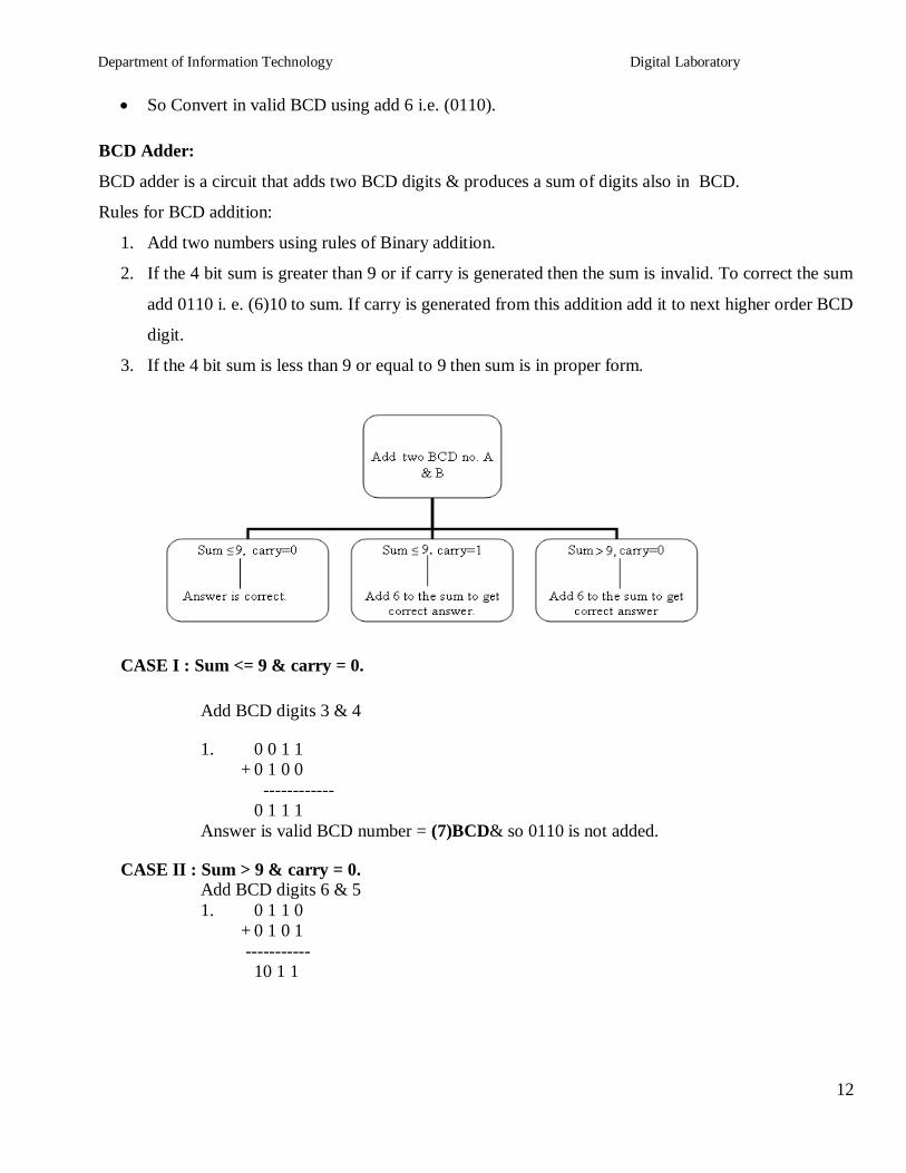
Department of Information Technology Digital Laboratory
12
So Convert in valid BCD using add 6 ie (0110)
BCD Adder
BCD adder is a circuit that adds two BCD digits amp produces a sum of digits also in BCD
Rules for BCD addition
1 Add two numbers using rules of Binary addition
2 If the 4 bit sum is greater than 9 or if carry is generated then the sum is invalid To correct the sum
add 0110 i e (6)10 to sum If carry is generated from this addition add it to next higher order BCD
digit
3 If the 4 bit sum is less than 9 or equal to 9 then sum is in proper form
CASE I Sum lt= 9 amp carry = 0
Add BCD digits 3 amp 4
1 0 0 1 1
+ 0 1 0 0
------------
0 1 1 1
Answer is valid BCD number = (7)BCDamp so 0110 is not added
CASE II Sum gt 9 amp carry = 0
Add BCD digits 6 amp 5
1 0 1 1 0
+ 0 1 0 1
-----------
10 1 1
Department of Information Technology Digital Laboratory
13
Invalid BCD (since sum gt 9) so 0110 is to be added
2 1 0 1 1
+ 0 1 1 0
-----------
1 0 0 0 1
(1 1)BCD
Valid BCD result = (11) BCD
CASE III Sum lt = 9 amp carry = 1
Add BCD digits 9 amp 9
1 1 0 0 1
+1 0 0 1
-----------
1 0 0 1 0
Invalid BCD ( since Carry = 1 ) so 0110 is to be added
2 1 0 0 1 0
+ 0 1 1 0
------------
1 1 0 0 0
(1 8)BCD
Valid BCD result = (18) BCD
Design of BCD adder
1 To execute first step i e binary addition of two 4 bit numbers we will use IC 7483
( withCin = 0 ) which is 4 bit binary adder
2 We need to design a digital circuit which will sense sum amp carry of IC 7483 amp if sum exceeds 9 or
carry = 1 this digital circuit will produce high output otherwise its output will be zero
Circuit to check invalid BCD
Department of Information Technology Digital Laboratory
14
First we will design circuit to check sum amp then we will logically OR output of this circuit to carry
output of IC 7483
For digital circuit which we are going to design we will have 4 inputs
( S3 S2 S1 S0) amp only 1 output Y
a) Y output of this circuit Will be ORed with carry output of first adder IC
7483
b) If BCD result is invalid i e sum output of first 7483 we have to add
(6)10 ie (0110)2 that means we need one more binary adder IC 7483
c) If BCD result is valid ( ie final output of the circuit to check validity is 0) we will make an
arrangement that second adder IC 7483 adds (0)10 i e ( 0000 )2 to the sum of the first adder IC 7483
The output of the combinational circuit is used as final output carry amp carry output of second adder IC is
ignored
i ) Truth Table for design of combinational circuit for BCD adder to check invalid
BCD
K-map for output- Y=S3S2+S3S1
Department of Information Technology Digital Laboratory
15
iii) Circuit diagram
v) Hardware Requirements
GATE Quantity
IC Quantity
Binary adder 2 7483 2
AND 2 7408 1
OR 2 7432 1
B ) Design and Implement single digit EXCESS-3 adder using IC 7483
Excess-3 code is a non weighted code It is a modified form of a BCD code The Excess-3 code can be
derived from the natural BCD code by adding 3 to each coded number It is also known as Self
Complementary code
Excess-3 code is a self complementary code because 1rsquos complement of Excess-3 number is Excess-3
code for the 9rsquos complement of corresponding number
Output of BCD adder
Department of Information Technology Digital Laboratory
16
Eg Excess-3 code for (4)10 is (0111)XS-3 1rsquos complement of this number is 1000 which is Excess-3 code
for (5)10and 5 is 9rsquos complement of (4)10
Rules for Excess-3 addition
i Add two Exceess-3 numbers
ii If carry is 1 add 3 to Sum
iii If carry is 0 subtract 3 from sum
Eg (8)10 + (6)10
(8)10 = 1011 (Excess-3 for 8)
(6)10= 1001 (Excess-3 for 6)
_______________
1 0100
0011 0011
_______________
0100 0111 ( Excess 3 code for (14)10
(i)Design
1) 4 bit Binary addition of excess 3 codes of two operands can be implemented with IC 7483
2) We have to design the circuit which will either add 0011 or subtract 0011 ie add 1101 (2rsquos
complement of 0011)depending upon carry bit
Letrsquos compare 0011 and 1101
B3 B2 B1 B0
0 0 1 1 ------- When carry is 1
1 1 0 1 ------- When carry is 0
Here B0 bit in both situation is High
Now compare B3 B2 and B1 It is complement of each other
When carry is 1 Bit B1 =1 B2=B3=0
When carry is 0 Bit B1 =0 B2=B3=1
B1 bit follows the carry and B2 and B3 bit complements the carry
(ii) Circuit Diagram
Department of Information Technology Digital Laboratory
17
(iii ) HARDWARE REQUIREMENTS
Sl No IC Description Quantity
1 7404 Not Gate 01
2 7483 4 bit Binary Adder 04
CONCLUSION
BCD adder ampsubtractor is designed amp tested for all possible combinations
FAQrsquos
1 Explain and Write the significance of BCD number system
2 Write the applications of BCD amp Excess 3 code
3 Explain the rules of BCD amp Excess 3 arithmetic
4 What is the difference between BCD and binary codes
5 What do you mean by unpacked and packed BCD nos
Department of Information Technology Digital Laboratory
18
Regularity Content Viva-voce Timely
Submission Total
Dated Sign of
Subject
Teacher
2 4 2 2 10
+
Date of Performance Date of Completion
-------------------------------------------------------------------------------------------------------------------
Assignment No 3
---------------------------------------------------------------------------------------------------------------------------
Title Implementation of logic functions
----------------------------------------------------------------------------------------------------------------------
Objective 1 To study the difference between multiplexer demultiplexer and decoder
2To study the applications of multiplexer
---------------------------------------------------------------------------------------------------------------------
Problem Statement Implement of Logic function using multiplexer IC 74153
---------------------------------------------------------------------------------------------------------------------
Hardware Requirement
i) IC 74153 74138 7404 7432
ii) Digital Trainer Kit -1
iii) Patch cords
----------------------------------------------------------------------------------------------------------------
Software Requirement Digital Work 30
------------------------------------------------------------------------------------------------------------------
Theory
D CWigital Multiplexer
Multiplexer are combinational digital circuits equating as controlled switches with several data inputs (I0
I1 I2 hellip) amp one single data output (ldquooutrdquo)At any time one of the Ip is transmitted to output According to
binary signals applied on control pairs to circuit Usually the number of data inputs is a power of two
Multiplexing is the process of transmitting a large no of information units over a small no of channel
digital multiplexer is a combinational large circuit which performs the operation of multiplexing It selects
Department of Information Technology Digital Laboratory
19
the operation of multiplexing It selects the operation of binary information from one of the many input
lines amp transfer to a single op line Multiplexer is called a data selector or multiposition switch because it
selects one of the many input Selection of a particular line is controlled by a set of a selection lines or
selects inputs The number of select lines depends upon no of input lines Generally there
is lsquonrsquo selects line for lsquomrsquo input lines By applying a particular code on select lines is transmitted on the
output linesBlock diagram of MUX is shown at contains lsquo2mrsquo input lines lsquomrsquo select Such that 2m = n amp
one unable input which is used to activate or dedicate MUX Depending upon the no of IP amp OP lines
various types of multiplexers are available We have 21 41 81 161 MUX Here the first no indicates
the no of input lines amp second no indicates the no of output lines
E is called as enable input which is generally active low
Fig-Block diagram for N1 Multiplxer
Demultiplexer
Demultiplexer is a logic used to perform exactly reverse function performed by multiplexer It accepts a
single input and distributes among several outputs The selection of a particular output line is controlled
by a set of selection line There are n input lines amp 2m is the number of selection line whose bit
combinations determine which output to be selected
Encoder amp Decoder
1 Encoders are used to encode given digital number into different numbering format like
decimal to BCD Encoder Octal to Binary
2 Decoders are used to decode a coded binary word like BCD to seven segment decoder
3 Thus encoder and decoder are application specific logic develop we can not use any type of
input for any encoder and decoder
Smhelliphellips1 s0
Output(Y)
D0
D1
D2
D3
Dn
N1
multiplxer
E
Department of Information Technology Digital Laboratory
20
4 Need to select input according to encoder and decoder being selected for a particular
application as mention in examples above
Uses of Mux
1 Use for Boolean function implementation
2 Construct a common bus system
3 To select between multiple sources amp signal destination
4 Inter register transfer
Advantages
1) Simplification of logic expression not required
2) Logic design is simplified
Disadvantage
Only one function can be implemented using one MUX Hence they canrsquot be used in
combinational logic circuit which contains many function
Part-A (IC 74153)
1 VERIFICATION OF IC 74153
IC 74153 is a dual layer 41 MUX It has four input lines for (I0D-I3D) for second MUX amp active high
output lsquoYarsquo lsquoYbrsquo (1Y or 2Y) It has select lines S1S0 common to both MUX The Enable inputs are
active low EaampEb(1G and 2G) The MUX is activated when they are at logic o
Pin out of IC 74153
Department of Information Technology Digital Laboratory
21
Function table of IC 74153 (X= Donrsquot Care Condition)
Select Input
Inputs (I or II) Output
S1 S0 E (I or II) D0 D1 D2 D3 Y
X X 1 X X X X 0
0 0 0 0 X X X 0
0 0 0 1 X X X 1
0 1 0 X 0 X X 0
0 1 0 X 1 X X 1
1 0 0 X X 0 X 0
1 0 0 X X 1 X 1
1 1 0 X X X 0 0
1 1 0 X X X 1 1
2CASCADING OF IC 74153
Cascading is done to expand two or more MUX ICrsquos to a digital multiplexer with larger no of inputs ie
multiplexer stocks or tress is designed The enable input is used for cascading In case of IC 74153 we
have only two select lines But for certain application 3 select lines are required then it can be
obtained by cascading using enable Now with 3 select lines we have 8 combinations Out of this
combination the MSB is O MSB is 1 for last four combination so we can use these MSB to select
any 1 MUX out of two by connecting it to E pin of first 41 MUX
Function table of IC 74153 as 8 1 Mux by cascading 2 41 Mux
Select Input Output
C (1G 2G ) B (S1) A (S0) Y
0 0 0 D0
0 0 1 D1
0 1 0 D2
0 1 1 D3
1 0 0 D4
1 0 1 D5
Department of Information Technology Digital Laboratory
22
1 1 0 D6
1 1 1 D7
3FUNCTION IMPLEMENTATION
Y= sum m (1 3 5 6)
Thisexpression is in Standard SOP form and it is three variable function So we need to use mux with
three select inputs ie 81 Mux Already we have implemented 81 Mux using IC 74153 For Boolean
function in Standard SOP form we connect data inputs corresponding to the minterms present in the given
function to Vcc and remaining data inputs to ground
Truth table
Inputs Output
C B A Y
0 0 0 0
0 0 1 1
0 1 0 0
0 1 1 1
1 0 0 0
1 0 1 1
1 1 0 1
1 1 1 0
LOGIC DIAGRAM
Hardware Requirements
GATE Quantity
IC Quantity
Mux 1 74153 1
NOT 1 7404 1
OR 1 7432 1
Department of Information Technology Digital Laboratory
23
Part-B Decoder (IC 74138)
Theory
Discrete quantities of information are requested in digital system with binary codes A binary code of n
bits is capable of representing into 2n distinct elements of the coded information
Decoder converts coded input to coded outputs accepts one of the code
There are different types of decoders such as 38 decoder 416 line decoders etc These are in general
called as n m line decoder where m=2n and n= no of input lines and m=no of output lines Demux also
takes one input data line source and selectively distributes it to one of n output channels The only
difference between demux and decoder is that demux has Din (data ip) line whereas decoder does not
have
ADVANTAGES
1) The decoder provides best implementation whenever there are many outputs of the combinational
circuit and each op of the function (or its complement) is required to be expressed with a small no
of minterms
2) The decoder can function as demux If the Enable ip line is taken as Din (data ip)
DISADVANTAGES
Since decoder method requires an OR gate for each op function so there is new hardware used And it is
always advisable to use minimum hardware as we come across problems like propagation delay of gates
APPLICATIONS
Decoder is worthily used for decoding binary information and memory interfacing It is used for the
implementation of Boolean function
Differentiate between Mux Demux Decoder
Point Multiplexer Demultiplexer Decoder
Input Many input lines Single input line Many input line also Acts as select line
Output Single output line Many output line Many output lineActive low output
Select line 2m = n n = 2m Enable inputs used
Department of Information Technology Digital Laboratory
24
A) Verification of IC 74138
We use IC 74138 which accepts 3 binary weighted inputs (A0 A1 A2) and when enabled provides
mutually exclusive active low outputs (y0-y7) It features 3 Enable ips Two active low (G2A G2B) and
one active high (G1) Every output will be high unless G2A G2Bare low and G1 is high It has
demultiplexing capability and multiple enable ips for easy expansion
IC Diagram
Function Table of 38 decoder
Input Output
Enable Data
G2A G2B G1 A2 A1 A0 Y0 Y1 Y2 Y3 Y4 Y5 Y6 Y7
0 0 0 X X X 1 1 1 1 1 1 1 1
0 1 1 X X X 1 1 1 1 1 1 1 1
1 0 1 X X X 1 1 1 1 1 1 1 1
1 1 1 X X X 1 1 1 1 1 1 1 1
Department of Information Technology Digital Laboratory
25
0 0 1 0 0 0 0 1 1 1 1 1 1 1
0 0 1 0 0 1 1 0 1 1 1 1 1 1
0 0 1 0 1 0 1 1 0 1 1 1 1 1
0 0 1 0 1 1 1 1 1 0 1 1 1 1
0 0 1 1 0 0 1 1 1 1 0 1 1 1
0 0 1 1 0 1 1 1 1 1 1 0 1 1
0 0 1 1 1 0 1 1 1 1 1 1 0 1
0 0 1 1 1 1 1 1 1 1 1 1 1 0
B) Cascading of IC 74138
The enable ip G1 active high of IC 74138 is used for cascadingfor cascading 2 ICrsquos the enable ip G1 of
first IC is connected to G1 enable ip of second IC through a NOT gate This enable ip is used as MSB
select ip line A3 the other three select input lines of both ICrsquos (A0A1A2) are also shorted to select
input lines of second IC to get single ip select lines (A0A1A2)
The ip line A3 is used to enable disable the 2 IC 74138 decoders When A3=0 first IC is enabled and
second is disabled Thus the first decoder will generate minterms from 0000 to 0111 as op and the second
decoder will generate nothing When A3=1 the enable conditions are reversed and thus second decoder
IC will generate minterms 1000 to 1111
Function Table of 416 decoder using IC 74138 (38 decoder)
Input Output
Enable Data
G2
A
G2
B
A
3
A
2
A
1
A
0
Y
0
Y
1
Y
2
Y
3
Y
4
Y
5
Y
6
Y
7
Y
8
Y
9
Y1
0
Y1
1
Y1
2
Y1
3
Y1
4
Y1
5
0 1 X X X X 1 1 1 1 1 1 1 1 1 1 1 1 1 1 1 1
Department of Information Technology Digital Laboratory
26
1 0 X X X X 1 1 1 1 1 1 1 1 1 1 1 1 1 1 1 1
1 1 X X X X 1 1 1 1 1 1 1 1 1 1 1 1 1 1 1 1
0 0 0 0 0 0 0 1 1 1 1 1 1 1 1 1 1 1 1 1 1 1
0 0 0 0 0 1 1 0 1 1 1 1 1 1 1 1 1 1 1 1 1 1
0 0 0 0 1 0 1 1 0 1 1 1 1 1 1 1 1 1 1 1 1 1
0 0 0 0 1 1 1 1 1 0 1 1 1 1 1 1 1 1 1 1 1 1
0 0 0 1 0 0 1 1 1 1 0 1 1 1 1 1 1 1 1 1 1 1
0 0 0 1 0 1 1 1 1 1 1 0 1 1 1 1 1 1 1 1 1 1
0 0 0 1 1 0 1 1 1 1 1 1 0 1 1 1 1 1 1 1 1 1
0 0 0 1 1 1 1 1 1 1 1 1 1 0 1 1 1 1 1 1 1 1
0 0 1 0 0 0 1 1 1 1 1 1 1 1 0 1 1 1 1 1 1 1
0 0 1 0 0 1 1 1 1 1 1 1 1 1 1 0 1 1 1 1 1 1
0 0 1 0 1 0 1 1 1 1 1 1 1 1 1 1 0 1 1 1 1 1
0 0 1 0 1 1 1 1 1 1 1 1 1 1 1 1 1 0 1 1 1 1
0 0 1 1 0 0 1 1 1 1 1 1 1 1 1 1 1 1 0 1 1 1
0 0 1 1 0 1 1 1 1 1 1 1 1 1 1 1 1 1 1 0 1 1
0 0 1 1 1 0 1 1 1 1 1 1 1 1 1 1 1 1 1 1 0 1
0 0 1 1 1 1 1 1 1 1 1 1 1 1 1 1 1 1 1 1 1 0
C) Implementation of Boolean function
The procedure for implementation of combinational circuit by means of a decoder and lsquoORrsquo gates requires
that the Boolean function fir the circuit be expressed in Sum of Minterms These forms can be obtained by
Department of Information Technology Digital Laboratory
27
expanding the function A decoder is then chosen which generates all the minterms of n ip variables The
ip to each OR gate are selected from the decoder outputs according to the minterms list in each function
i) F1=summ (1 3 5 7)
Truth table
Logic Diagram
ii) F2=summ (1 3 5 7111315)
Truth table
Logic Diagram
Conclusion In this way multiplexer Decoderamp its applications are studied implemented amp
tested
FAQrsquos
1What is a multiplexer
2What is a Demultiplexer
3 Enlist applications of multiplexer
Department of Information Technology Digital Laboratory
28
Regularity Content Viva-voce Timely
Submission Total
Dated Sign of
Subject
Teacher
2 4 2 2 10
Date of Performance Date of Completion
-------------------------------------------------------------------------------------------------------------------
Assignment No4
------------------------------------------------------------------------------------------------------------------
Title 3 bit updown Asynchronous and Synchronous counter using IC7476
------------------------------------------------------------------------------------------------------------------
Objective To understand design procedure of asynchronousamp Synchronous counter
------------------------------------------------------------------------------------------------------------------
Problem Statement Design (State diagram state table amp K map) and implementation of 3
bit Up and Down Asynchronous and Synchronous Counter using master slave JK flip-flop IC 7476
-----------------------------------------------------------------------------------------------------------------
Hardware Requirement
i) IC 7476 (MS-JK Flip-flop) IC 7408(Quad 2 ip AND Gate)
IC 7432 (Quad 2 ip OR Gate) and IC 7404 (Hex Inverter)
ii) Digital Trainer Kit -132
iii) Patch cords
----------------------------------------------------------------------------------------------------------------
Software Requirement Digital Work 30
------------------------------------------------------------------------------------------------------------------
Theory
Counters counters are logical device or registers capable of counting the no of states or no of clock
pulses arriving at its clock input where clock is a timing parameter arriving at regular intervals of time
so counters can be also used to measure time amp frequencies They are made up of flip flops Where the
Department of Information Technology Digital Laboratory
29
pulse are counted to be made of it goes up step by step amp the op of counter in the flip flop is decoded to
read the count to its starting step after counting n pulse incase of module counters
Types of Counters
Counter are of two types
1) Asynchronous counter
2) Synchronous counter
Asynchronous counter
A digital counter is a set of flip flop The flip flop are connected such that their combined state at any time
is binary equivalent of total no of pulses that have occurred up to that time Thus its name implies a
counter is used to count pulse A counter is used as frequency dividers To obtain waveform with
frequency that is specific fraction of clock frequency
Counter may be Asynchronous or synchronous The Asynchronous counter is also called as ripple counter
An Asynchronous counter uses T flip flop to perform a counting function The actual hardware used is
usually J-K flip flop with J amp K connected to logic1Even D flip flops may be used here
In asynchronous counter commonly called ripple counter the first flip-flop is clocked by the external
clock pulse amp then each successive flip-flop is clocked by the Q or Qrsquo output of the previous flip-flop
Therefore in an asynchronous counter the flip-floprsquos are not clocked simultaneously The input of MS-JK
is connected to VCC because when both inputs are one output is toggled As MS-JK is negative edge
triggered at each high to low transition the next flip-flop is triggered
Synchronous Counter
When counter is clocked such that each flip flop in the counter is
triggered at the same time the counter is called as synchronous counter
The gates propagation delay at reset time will not be present or we may say will not occur
1) Asynchronous Up Counter
Fig 1 shows 3bit Asynchronous Up Counter Here Flip-flop 2 act as a MSB Flip-flop and Flip-flop 0 act
as a LSB Flip-flop Clock pulse is connected to the Clock of Flip-flop 0 Output of Flip-flop 0(Q0) is
connected to clock of next flip-flop (ie Flip-flop 1) and so on As soon as clock pulse changes output is
going to change (at the negative edge of clock pulse) as a Up count sequence For 3 bit Up counter state
table is as shown below
Department of Information Technology Digital Laboratory
30
State Table
Logic diagram
Fig 1 3 Bit Asynchronous Up Counter
Hardware requirements
Gate
Flip flop
Quantity IC Quantity
MS JK 3 7476 2
2) Down Counter
Fig 2 shows 2 bit Asynchronous Down Counter Here Flip-flop 2 act as a MSB Flip-flop and Flip-flop 0
act as a LSB Flip-flop Clock pulse is connected to the Clock of Flip-flop 0 Output of Flip-flop 0 (Q0rsquo) is
Counter States Count
Q2 Q1 Q0
0 0 0 0
1 0 0 1
2 0 1 0
3 0 1 1
4 1 0 0
5 1 0 1
6 1 1 0
7 1 1 1
8 0 0 0
Department of Information Technology Digital Laboratory
31
connected to clock of next flip-flop (ie Flip-flop 1) and so on As soon as clock pulse changes output is
going to change (at the negative edge of clock pulse) as a down count sequence For 3 bit down counter
sate table is as shown below
In both the counters Inputs J and K are connected to Vcc hence J-K Flip flop work in toggle mode Preset
and Clear both are connected to logic 1
State Table
Logic diagram
Fig 2 3 Bit Asynchronous Down Counter
Hardware requirements
Counter States Count
Q2 Q1 Q0
7 1 1 1
6 1 1 0
5 1 0 1
4 1 0 0
3 0 1 1
2 0 1 0
1 0 0 1
0 0 0 0
7 1 1 1
Department of Information Technology Digital Laboratory
32
Gate
Flip flop
Quantity IC Quantity
MS JK 3 7476 2
Applications
The asynchronous counters are specially used as the counting devices
They are also used to count number of pulses applied
It also works as frequency divider
It helps in counting the number of product coming out of the machinery where product is coming out at
equal interval of time
Types of synchronous counter
1) Up counter
2) Down counter
1 3 bit Synchronous up counter
The up counter counts from 0 to7 ie(000 to 111)for this we are using MS JK flip flop In IC 74LS76 2
MS J-K flip flops are present The clock pulse is given at pin 1 amp 6 of the 1st IC amp pin 1 of 2nd IC Next
state decoder logic is designed with the help of state table
State table for synchronous up counter
Present state Next state Flip flop 3 Flip flop 2 flip flop 1
Q2 Q1 Q0 Q2 Q2 Q0 J2 K2 J1 K1 J0 K0
0 0 0 0 0 1 0 x 0 X 1 x
0 0 1 0 1 0 0 x 1 X x 1
0 1 0 0 1 1 0 x x 0 1 x
0 1 1 1 0 0 1 x x 1 x 1
1 0 0 1 0 1 x 0 0 X 1 X
1 0 1 1 1 0 x 0 1 X x 1
1 1 0 1 1 1 x 0 x 0 1 X
1 1 1 0 0 0 x 1 x 1 x 1
Department of Information Technology Digital Laboratory
33
K-Map
Q1Q0
Q2
00 01 11 10
0 0 0 1 0
1 X X X X
J2= Q1Q0
Q1Q0
Q2
00 01 11 10
0 X X X X
1 0 0 1 0
K2= Q1Q0
Q1Q0
Q2
00 01 11 10
0 0 1 X X
1 0 1 X X
J1= Q0
Q1Q0
Q2
00 01 11 10
0 X X 1 0
1 X X 1 0
K1= Q0
Department of Information Technology Digital Laboratory
34
Q1Q0
Q2
00 01 11 10
0 1 X X 1
1 1 X X 1
J0= 1
Q1Q0
Q2
00 01 11 10
0 X 1 1 X
1 X 1 1 X
K0= 1
Logic Diagram
Fig 1 3 bit Synchronous up counter
Department of Information Technology Digital Laboratory
35
2 3 bit Synchronous down counter
This is used to count from 7-0 ie(111-000)for this also 2 ICrsquos of 74LS76 are required amp hence we use 3
MS JK flip flops Here also clock is given to 1stamp 6th pin of 1st IC amp1st pin of 2nd IC enabling to apply
clock to all flip flop at a time Next state decoder logic is designed with the help of state table
State table for synchronous down counter
Present state Next state Flip flop 3 Flip flop 2 Flip flop 1
Q2 Q1 Q0 Q2 Q1 Q0 J2 K2 J1 K1 J0 K0
1 1 1 1 1 0 X 0 X 0 X 1
1 1 0 1 0 1 X 0 X 1 1 X
1 0 1 1 0 0 X 0 0 X X 1
1 0 0 0 1 1 X 1 1 X 1 X
0 1 1 0 1 0 0 X X 0 X 1
0 1 0 0 0 1 0 X X 1 1 X
0 0 1 0 0 0 0 X 0 X X 1
0 0 0 1 1 1 1 X 1 X 1 X
K-Map
Q1Q0
Q2
00 01 11 10
0 1 0 0 0
1 X X X X
J2= Q1Q0
Q1Q0
Q2
00 01 11 10
Department of Information Technology Digital Laboratory
36
0 X X X X
1 1 0 0 0
K2= Q1Q0
Q1Q0
Q2
00 01 11 10
0 1 0 X X
1 1 0 X X
J1= Q0
Q1Q0
Q2
00 01 11 10
0 X X 0 1
1 X X 0 1
K1= Q0
Q1Q0
Q2
00 01 11 10
0 1 X X 1
1 1 X X 1
J0= 1
Q1Q0
Q2
00 01 11 10
0 X 1 1 X
1 X 1 1 X
K0= 1
Department of Information Technology Digital Laboratory
37
Logic Diagram
Fig 2 3 bit Synchronous down counter
Uses
1 Specially used as the counting devices
2 Used in frequency divider circuit
3 Used in digital voltmeter
4 Used in counter type A to D converter
5 Used for time measurement
6 It helps in counting the no of product coming out from machinery where product is coming out
at equal interval of time
Conclusion
Up and down counters are successfully implemented the counters are studied amp op are checked The
state table is verified
PRACTICE ASSIGNMENTS EXERCISE MODIFICATIONS
1 Design amp implement 2 bit controlled synchronous counter
2 Designamp implement 4 bit controlled synchronous counter
3 Designamp implement truncated synchronous up or down counter
FAQrsquos with answers
1 What do you mean by Counter
A Counter is a register capable of counting the no of clock pulses arriving at its
clock inputs Count represents the no of clock pulses arrived A specified
sequence of states appears as the counter output
Department of Information Technology Digital Laboratory
38
2 What are the types of Counters Explain each
There are two types of counters as Asynchronous Counter and Synchronous Counter
Asynchronous Counter In this counter the first flip-flop is clocked by the external clock pulse
and then each successive flip-flop is clocked by the Q or Qrsquo op of the previous flip-flop Hence in
Asynchronous Counter flip-flops are not clocked simultaneously and hence called as Ripple
Counter Synchronous Counter In this counter the common clock input is connected to all the
flip-flops simultaneously
3 What do you mean by pre-settable counters
A counter in which starting state is not zero can be designed by making use of the
preset inputs of the flip flops This is referred to as loading the counter
asynchronously This is referred to as pre-settable counter
4 What are the applications of synchronous counters
Digital clock
Frequency divider circuits
Frequency counters
Used in analog to digital converters
5 What are the advantages of synchronous counters over asynchronous counters
Propagation delay time is reduced
Can operate at a much higher frequency than the asynchronous counters
6 Ring counter is an example of synchronous counters or asynchronous counter
Synchronous counter Since all the flip flops are clocked simultaneously
7 Twisted Ring (Johnsonrsquos) counter is an example of synchronous counters or asynchronous
counter
Synchronous counter Since all the flip flops are clocked simultaneously
8 What is the difference between ring counter and twisted ring counter
In ring counter pulses to be counted are applied to a counter it goes from state to state and the
output of the flip flop s in the counter is decoded to read the count Here the uncomplimentary
output (Q) of last flip flop is fed back as an input to first flip flop Ring counters are referred as
MOD lsquoNrsquo counters
Department of Information Technology Digital Laboratory
39
But in Twisted ring counter the complimentary output (Q bar) of last flip flop is fed back as an
input to first flip flop Twisted Ring counters are referred as MOD lsquo2Nrsquo counters
9 What are the applications of ring counters
Ring counter outputs are sequential non-overlapping pulses which are useful for control state
counters Used in stepper motor this requires pulses to rotate it from one position to the next Used
as divide by lsquoNrsquo ((MOD lsquoNrsquo) counters
10 What are the applications of ring counter twisted ring counters
Used as divide by lsquo2Nrsquo ((MOD lsquo2Nrsquo) counters
Used for control state counters
Used for generation of multiphase clock
11 List the Synchronous Counter ICs
IC 74160 Decade Up Counter
IC 74161 4 bit binary Up Counter
IC 74162 Decade Up Counter
IC 74163 4 bit binary Up Counter
IC 74168 Decade UpDown Counter
IC 74169 4 bit Binary UpDown Counter
IC 74190 Decade UpDown Counter
IC 74191 4 bit Binary UpDown Counter
IC 74192 Decade UpDown Counter
IC 74193 4 bit Binary UpDown Counter
Department of Information Technology Digital Laboratory
40
Regularity Content Viva-voce Timely
Submission Total
Dated Sign of
Subject
Teacher
2 4 2 2 10
Date of Performance Date of Completion
-------------------------------------------------------------------------------------------------------------------
Assignment No 5
-------------------------------------------------------------------------------------------------------------------------------
Title Design and implementation of Module lsquonrsquo counter with IC7490 and IC 74191
-----------------------------------------------------------------------------------------------------------------------------
Objective To know difference between regular amp truncated counter as well as binary ampBCD Counter
--------------------------------------------------------------------------------------------------------------------------------
Problem Statement To design and implement mod - 10 mod ndash 7 mod - 99 asynchronous BCD
counter using IC 7490 and to design and implement up down mod - n Binary counter using IC 74191
-----------------------------------------------------------------------------------------------------------------
Hardware Requirement
i) IC 7490 IC 74191 basic gates
ii) Digital Trainer Kit -1
iii) Patch cords
----------------------------------------------------------------------------------------------------------------
Software Requirement Digital Work 30
------------------------------------------------------------------------------------------------------------------
Theory
Part A ndash IC 7490
IC 7490 is a TTL MSI (medium scale integration) decade counter It contains 4 master slave flip flops
internally connected to provide MOD-2 ie divide by 2 and MOD-5 ie divide by 5 counters MOD-2 and
Mod-5 counters can be used independently or in cascading
Department of Information Technology Digital Laboratory
41
It is a 4-bit ripple type decade counter The device consists of 4-master slave flip flops internally
connected to provide a divide by two and divide by 5 sections Each section has a separate clock ip to
initiate state changes of the counter on the high to low clock transition
Since the op from the divide by 2 section is not internally connected to the succeeding stages The device
may be operated in various counting modes In a BCD counter the CP1 input must be externally connected
to QA op The CP0ip receives the incoming count producing a BCD count sequence It is also provided
with additional gating to provide a divide by 2 counter and binary counter for which the count cycle length
is divide by 5 The device may be operated in various counting modes
There are 2 reset inputs R0(1) and R0(2) both of which need to be connected to the lsquologic 1rsquo for clearing all
flip flops Two set inputs Rg(1) and Rg(2) when connected to logic 1 are used for setting counter to 1001
(BCD 9)
Pin out of IC 7490
Fig Pin configuration of IC7490
Table 1-pin name and description of IC7490
Pin name Description
Input B This is clock input to the internal MOD-5 ripple counter which is negative
edge triggered
R0(1)R0(2) Gated zero reset inputs
Department of Information Technology Digital Laboratory
42
R9(1)R9(2) These are gated set to nine inputs
QDQCQB Output of internal MOD-5 counter with QD as MSB
QA Output of internal MOD-2 counter with QA as LSB
Input A Clock input to FF-A which is negative edge triggered
Functional Table for IC7490
Reset inputs Output
R0(1) R0(2) R9(0) R9(1) QD QC QB QA
1 1 0 X 0 0 0 0
1 1 X 0 0 0 0 0
X X 1 1 1 0 0 1
X 0 X 0 COUNTER
0 X 0 X COUNTER
0 X X 0 COUNTER
X 0 0 x COUNTER
Department of Information Technology Digital Laboratory
43
Basic internal Structure of IC 7490
Function Table of MOD-5 counter
Design of MOD-10 counter using IC 7490
The QA op the first flip flop is connected to the input B which is clock ip of internal MOD-5 ripple
counter Due to cascading of Mod-2 and Mod-5 counters the overall configuration the decade counters
count from 0000 to 1001 After 1001 mod-5 resets to 0000 and next count after 1001 is 0000
When QA op is connected to B ip we have the Mod-2 counter followed by Mod-5 counter The
count sequence obtained is shown in the table It may be noted that QA changes from 0 to 1 the state of
InputB clock Output
Count QD QC QB
0 0 0 0
0 0 1 1
0 1 0 2
0 1 1 3
1 0 0 4
Department of Information Technology Digital Laboratory
44
Mod-5 counter doesnrsquot change whereas when QA changes from 1 to 0 the Mod-5 counter goes to the next
state
Logic DiagramMOD-10 counter using IC 7490
5 Modulus n Counter
Function table
Ip clock
Output
Count QD QC QB QA
0 0 0 0 0
0 0 0 1 1
0 0 1 0 2
0 0 1 1 3
0 1 0 0 4
Department of Information Technology Digital Laboratory
45
Design of Mod-7 Counter using IC 7490
Mod-7 counter counts through seven states from 0 to 6 counters and it should reset as soon as the
count becomes 7 The op of reset logic should be 1 corresponding to invalid states The reset logic op
should be applied to pin 2 and 3
Truth Table of Reset Logic
0 1 0 1 5
0 1 1 0 6
0 1 1 1 7
1 0 0 0 8
1 0 0 1 9
QD QC QB QA Y
0 0 0 0 0
0 0 0 1 0
0 0 1 0 0
0 0 1 1 0
0 1 0 0 0
0 1 0 1 0
0 1 1 0 0
0 1 1 1 1
1 0 0 0 1
1 0 0 1 1
Department of Information Technology Digital Laboratory
46
Logic Diagram Mod 7 Counter using IC 7490
Function table
Ip clock
Output
Count QD QC QB QA
0 0 0 0 0
0 0 0 1 1
0 0 1 0 2
0 0 1 1 3
0 1 0 0 4
0 1 0 1 5
0 1 1 0 6
Department of Information Technology Digital Laboratory
47
Design of Mod-99 using IC 7490
For Mod-99 two IC 7490rsquos will be required Hence to implement a divide by 99 counter we have
to use two decade counters ICrsquos A divide by 99 counter counts 99 states from 0 to 98 and the counter
should reset as soon as the count becomes 99 So in order to reset the counter of 99 connect the Q op
which are equal to 1 in the count of 99 to an lsquoAndrsquo gate amp then connect and op to the reset ip of both
ICrsquos
MOD-100 Counter-
MOD-100 counter can be obtained by cascading two decade counter ICrsquos
Each IC gives divide by 10 counts Hence 2 ICs will give 1010=100 counts
Clock is applied to the input A of IC 7490 the Q1 output is connected to B input etc
For cascading the QD output of the first IC is connected to the input A of second IC Thus QD of
IC-(1) acts as clock input to IC-(2)
The Ro (1) Ro(2) R9(1) R9(2) inputs of both ICs are connected to ground so as to make them
inactive
The total count provided by the two counters varies from 00 to 99 decimal that means 100 states
Hence it is a MOD-10 counter
Impleacutementations
FigureMOD-100 counters using IC 7490
Department of Information Technology Digital Laboratory
48
B) IC 74191 ndash Theory
IC74191 is 4-bit binary synchronous reversible up down counter It contains 4 master slave flip flops
with internal gating and steering logic to provide asynchronous reset and synchronous count updown
operations its asynchronous parallel capability permits the counter to be preset to any desire number D0
to D3 are the parallel data inputs Information present on the parallel data inputs D0 to D3 is loaded into
the counter and appears on the output when the load PLinput is lowThisoperation overrides the counting
function Counting is inhabited by the high level on the enable G input when G input is low internal state
changes are initiated synchronously by the low to high transitions of the clock inputs the updown input
signal determines the direction of input
Function Table
Operating
mode
Inputs Outputs
PL UD G CLK Dn
Parallel
load L X X X L L
L X X X H H
Count up H L 0 uarr X Count up
Count
down H H 0 uarr X
Count
down
Hold(No
change) H X H X X No change
Pin details ndash
D0 to D3 input lines PL parallel load
G is Enable input ndash enabling the counting
Q0 to Q3 output lines
Downup determines the direction of counting
Clk clock input for counter
Terminal Count Max(1111) min(0000) For these states signal goes high for 1clock pulse
Ripple clock Clock input for next higher state
Department of Information Technology Digital Laboratory
49
Pin Diagram IC 74191
Up counter- Truth Table
Clk
Pulses QA QB QC QD
0 0 0 0 0
1 0 0 0 1
2 0 0 1 0
3 0 0 1 1
4 0 1 0 0
5 0 1 0 1
6 0 1 1 0
7 1 1 1 1
8 1 0 0 0
9 1 0 0 1
10 1 0 1 0
11 1 0 1 1
12 1 1 0 0
13 1 1 0 1
Department of Information Technology Digital Laboratory
50
14 1 1 1 0
15 1 1 1 1
Logic Diagram
Steps-
Connect the circuit as shown above
Apply clock ip to pin no14
Connect UD to GND
Verify the output according to truth table
Logic diagram of down counter
Steps-
Connect the circuit as shown above
Apply clock ip to pin no14
Connect UD to VCC
Verify the output according to truth table
UD D3 D2 D1 D0 PL
Clock IC 74191
G RC
MAX MIN
Q3 Q2 Q1 Q0 TC
vcc
NC
NC
Outputs
no connection
vcc
Department of Information Technology Digital Laboratory
51
With the help of IC74191 we can implement truncated updown counter by using following logic ndash
Connect data input line to particular count you want to load
According to requirement make Truth table
Draw the K-map
Find out Boolean expression
Draw the logic diagram and that is the combinational logic for your count and apply the output of
that circuit to PL
According to requirement we get the UP and down counting
5 Modulus n Counter
Presettable updown counter
Mod 11 counter
Implementation of presetttable mod updown counter using IC- 74LS191
1 Load Data on data lines D0 to D3 (0101)
2 Counter will go through the states from 0101 0110hellip1111 in up counter and 0101 to 0000 in
down counter
Combinational Circuit
CLOCK D3 D2 D1 D0
TC
U D 74191 RC
G PL
Updown Q3 Q2 Q1 Q0 PL
Q3 Q2 Q1 Q0
Preset Count
Department of Information Technology Digital Laboratory
52
3 The logic circuit should be designed in such a way that only when all the outputs are high output
of the reset circuit should be low and the counter should jump to state 5 It should again start
counting from 0101 to 0000
State Table
Down Counter UP Counter
IC 74191 is 4 bit counter Thus it counts 0000 to 1111 different 16 states For MOD11 counter we require
different 11 states so 5 steps must be skipped from 16 states We get MOD11 by presetting counter to
value 5
Assignment Question
Design and Implement MOD 7 MOD 10 and MOD 12 using IC 74191
FAQs
1 What do you mean modulus counter
Counter
state Clock
pulse
Q3 Q2 Q1 Q0
1 0 1 0 1
2 0 1 1 0
3 0 1 1 1
4 1 0 0 0
5 1 0 0 1
6 1 0 1 0
7 1 0 1 1
8 1 1 0 0
9 1 1 0 1
10 1 1 1 1
11 1 1 1 1
Counter state
Clock pulse
FF outputs
Q3 Q2 Q1 Q0
1 0 1 0 1
2 0 1 0 0
3 0 0 1 1
4 0 0 1 0
5 0 0 0 1
6 0 0 0 0
7 0 1 0 1
Department of Information Technology Digital Laboratory
53
It represents the number of possible states of counter
2 How will you use the 7490 IC to design symmetrical divide by 10 frequency counter
The divide by 5 circuit followed by divide by 2 circuit will give symmetrical output
3Where counters are used Give real life example of counter
Modulus n Counter
Binary counter ndash An N stage counter that recycles after 2 Ncount The count proceds in specified binary
sequence Counter Presetable- A counter which can be set to a desired value before the start of the
counting UPDown counter ndash A counter that can count in both up and down direction depending upon a
control input
Department of Information Technology Digital Laboratory
54
Regularity Content Viva-voce Timely
Submission Total
Dated Sign of
Subject
Teacher
2 4 2 2 10
Date of Performance Date of Completion
-------------------------------------------------------------------------------------------------------------------
Assignment No6
------------------------------------------------------------------------------------------------------------------
Title Sequence Generator
------------------------------------------------------------------------------------------------------------------
Objective To understand sequence generator one of the sequential circuit
-------------------------------------------------------------------------------------------------------------------
Problem Statement Design (State Diagram State Table K Map) and implementation of Sequence
Generator using Shift Register IC 74194
-----------------------------------------------------------------------------------------------------------------
Hardware Requirement
i) IC 741947408 (AND-gate) 7432 (OR-gate)
ii) Digital Trainer Kit -1
iii) Patch cords
----------------------------------------------------------------------------------------------------------------
Software Requirement Digital Work 30
------------------------------------------------------------------------------------------------------------------
Theory
Part A Sequence Generator with Flip flop
A sequential circuit which generates a prescribed sequence of bits in synchronism with a clock is referred
to as a sequence generator These pulse trains or sequence of bits can be used to open valves close gates
turn on lights and turn off machines and other variety of jobs
Department of Information Technology Digital Laboratory
55
For the design of sequence generator we first determine the required no of flip flops and the logic circuit
for the next state decoder
No of flip flops required to generate particular sequence can be determined as follows
1) Find the no of 1rsquos in the sequence
2) Find the no of 0rsquos in the sequence
3) Take the maximum out of two
4) If N is the required no of flip flops choose minimum value of lsquonrsquo to satisfy equation given below
Max (0rsquos 1rsquos) le 2n-1
The sequence generator can be classified as
1) sequence generator without bushing
2) sequence generator with bushing
The aim in this experiment is to design a sequence generator to generate a sequence of bit ie 10101
Part B Sequence Generator using Shift Register IC 74194
IC 74194 4 bit bidirectional Shift Register
This bidirectional shift register is designed to incorporate virtually all the features a system designer may
want in a shift register they feature Parallel inputs parallel outputs right shift left shift serialinputs
operating mode control inputsand a direct overriding clear line The register has four distinct modes of
operationsnamely
1 Parallel load
2 Shift right (in the direction QA towards QD)
3 Shift left (in the direction QD towards QA)
4 Inhibit clock (do nothing)
Synchronous parallel loading is accomplished by applying the four bits of data and taking both
mode control inputs S0 and S1High The data is loaded in to the associated flip-flops and appear
at the outputs after positive transition of the clock input During loading serial data flow is
inhibited
Shift right is accomplished synchronously with the rising edge of the clock pulse when S0 is High
and S1 is Low Serial data for this mode is entered at the shift right data input When S0 is Low
and S1 is High data shifts left synchronously and new data is entered at the shift left serial input
Clocking of the flip flop is inhibited when both mode control inputs are LOW
Department of Information Technology Digital Laboratory
56
Mode Control Input Operation
S1 S0
0 0 Clock Inhibit
0 1 Shift right
1 0 Shift Left
1 1 Parallel loading
Function Table of IC 74194
Design
The minimum number of flip-flops N required to generate a sequence of length S is given by S
le 2N ndash 1
In this case S=7 therefore the minimum value of N which may generate in this sequence is 3
However it is not guaranteed to lead to a solution If the given sequence leads to seven distinct
states then only three flip flops are sufficient otherwise we have to increase the number of flip
flops We write the states of circuit as given in table 1 The prescribed sequence is listed under QA
and the sequence listed under QB and QC are the same sequence delayed by one and two clock
pulses respectively From the table we observe that all the states are not distinct which means N=3
is not sufficient Next we assume that N=4 and prepare table 2 The last column gives the required
serial input for getting the desired change of state when a clock pulse is applied This is obtained
by assuming D type flip flop and looking at the QA output For example at the falling edge of first
clock pulse QA=1 The second clock pulse must result in QA=1 which requires its D input to be 1
In the same manner all the entries in column Y are determined
Table 1 State Assignment Table of Sequence Generator (N=3)
Number of Clock
Pulses
Flip Flop Inputs States
QA QB QC
1 1 1 1 7
2 1 1 1 7
3 0 1 1 3
4 1 0 1 5
Department of Information Technology Digital Laboratory
57
5 0 1 0 2
6 1 0 1 5
7 1 1 0 6
Excitation table of D Flip-Flop
Present State Qn Next State Qn+1 Flip-Flop Input D
0 0 0
0 1 1
1 0 0
1 1 1
Table 2State Assignment Table of Sequence Generator (N=4)
Number of Clock
Pulses
Flip Flop Inputs States
Y
Serial ip QA QB QC QD
1 1 1 1 0 14 1
2 1 1 1 1 15 0
3 0 1 1 1 7 1
4 1 0 1 1 11 0
5 0 1 0 1 5 1
6 1 0 1 0 10 1
7 1 1 0 1 13 1
K-Map Simplification
Department of Information Technology Digital Laboratory
58
00 01 11 10
00 X X X X
01 X 1 1 X
11 X 1 0 1
10 X X 0 1
Y= QArsquo + QBrsquo + QCrsquo = QAQBQC
LOGIC DIAGRAM
HARDWARE REQUIREMENTS
Sr no ICs Description Quantity
11 74194 4 bit bidirectional universal shift register 16ktr`
2 7410 3 input NAND Gate 1
Department of Information Technology Digital Laboratory
59
Conclusion In this way sequence generator using JK flip flips amp shift register is designed and
implemented
Enhancements Modifications ndash Sequence generator can also be implemented with shift register instead
of flip flops Use IC 7495 universal shift register IC and try to implement sequence generator
FAQs
1 What is sequential logic circuit
A sequential logic circuit consists of a memory elements in addition to
combinational circuit Its output at any instant of time depends upon
the present input as well as present state of memory element
2 What is meant by delay line
It is used to introduce time delays in digital signals
3 What is meant by following terms
a) Synchronous preset b) Asynchronous preset
c) Synchronous clear d) Asynchronous clear
a)Preset operation is synchronised with the clock
b)Preset operation is independent of the clock
c) clear is performed in synchronous with clock
d) clear is performed independent with clock
4 Is asynchronous counter faster than synchronous counter
In a synchronous counter the time required for change of any state is same and is equal to delay
time of one flip flop where as in asynchronous counter all flip flops are not clocked
simultaneously hence time required is not same
5 What is mean by lockout in counter
In a counter design for a fewer state than the maximum possible state some time it may so happen
that counter enters in unused state and goes from one unused state to another unused state and
never comes to used state
6 What is mean by state table
Department of Information Technology Digital Laboratory
60
It consists of complete information about present state and next state and outputs of a sequential
system
7 What is mean by state diagram
The information available in a state table can be represented as graphically the graphical
representation is known as state diagram
8 What is the advantage of state reduction in the design of sequential circuit
It reduces the number of flip flops
9 What is meant by excitation table
This gives information about what should be the flip flop inputs if outputs are specified before and
after the clock pulse
10 How many flip flops are required to design sequence generator using Counters
max (0rsquoS1rsquoS) in a given sequence lt= 2(N - 1)
Where N = Number of flip flops
11 How many flip flops are required to design sequence generator using shift registers
Slt= 2N - 1
Where N=Number of flip flops
S= Length of sequence
12 What is Lock out condition How it is avoided
When counter enters into one of the invalid state and after application of pulses remains in invalid
states only i e counter gets locked into invalid state amp this is called as lock out Lock out can be
avoided by providing bushing to all the invalid states in such a way that after application of one or
more clock pulses counter will fall into one of the valid state
Department of Information Technology Digital Laboratory
61
Regularity Content Viva-voce Timely
Submission Total
Dated Sign of
Subject
Teacher
2 4 2 2 10
Date of Performance Date of Completion
-------------------------------------------------------------------------------------------------------------------
Assignment No7
------------------------------------------------------------------------------------------------------------------
Title Multiplexer using Data flow modeling and structural modeling
------------------------------------------------------------------------------------------------------------------
Objective To learn data flow modeling style Its uses and different types of declarations with some
different types of circuits Structure of VHDL program is well discussed with this modeling style
-------------------------------------------------------------------------------------------------------------------
Problem Statement 41 multiplexer using data flow amp structural modeling -
----------------------------------------------------------------------------------------------------------------
Hardware Requirement - NA
----------------------------------------------------------------------------------------------------------------
Software Requirement Xilinx
------------------------------------------------------------------------------------------------------------------
Theory
Data flow style-
In this type of design the view of data as flowing from input to output through a design
An operation is defined in terms of a collection of data transformation expressed as concurrent
statement Each of the statement can be activated when any of its input signal changes its value While
these statements describe the behavior of the circuit a lot of information about its structure can be
extracted from the description as well
Data flow modeling has a set of concurrent assignment statements In the data flow level of abstraction we
describe how information is passed in the circuit The built in operators in VHDL are used in expression
such as AND OR XOR NOT etc
Department of Information Technology Digital Laboratory
62
INPUT
Two select lines S1S0
Four data lines D0 D1 D2 D3
OUTPUT
One output line Y
Functional block diagram of 41 Mux
Fig 41 Multiplexer using Data flow modeling
Function table of 41 Mux
Enable S1 S0 A B C D Y
1 X X X X X X 0
0 0 0 A X X X A
0 0 1 X B X X B
0 1 0 X X C X C
0 1 1 X X X D D
Design steps
Click on Xilinx ISE 92i
Create New project from file menu Ensure top level source is HDL
Select family of devices (usually spartan2E or 3)
Department of Information Technology Digital Laboratory
63
Ensure preferred language is VHDL
Click new source which shows you project details device details
and Synthesis and simulator tools
After finishing project create new source by right clicking in project name with VHDL
module
Complete ports name directions and bus Ensure architecture name is behavioral
After that we will get design summary and detailed reports
Close design summary
Create your code with given modeling style
Go to process window and synthesis to check if any error is there in code Check syntax and
view RTL schematic
Create new source to simulate the code
Right click on source name and create test bench waveform with proper name Ensure the
project is same
Click on combinational circuit in initial timing wizard
Select test bench wave in source window Apply inputs to wave diagram Ensure you are in
behavioral simulation
Go to process box Click on Xilinx ISE simulator and simulate the model See results
RTL Schematic
Department of Information Technology Digital Laboratory
64
Timing Diagram
FAQrsquos
1 What are the different kinds of data objects in VHDL code
Ans data object may be any value or number still some signal data objects and bit and bit_vector
types of these are available in VHDL STD_LOGIC and STD_LOGIC_VECTOR types are used
widely in programming
2 What do you mean by signal
Ans signal is a data object represents logic signals or wires in a circuit There are three places in
which signals can be declared in VHDL code in an entity declaration in the declarative section of
architecture and in declarative section of package
3 What are different signal types
Ans BIT BIT_VECTOR STD_LOGIC STD_LOGIC_VECTOR STD_ULOGIC SIGNED
UNSIGNED INTEGER ENUMERATION and BOOLEAN
4 What is an entity
Ans a circuit or sub circuit described with VHDL code is called a design entity
5 Explain structure of an entity
Ans it has two main parts the entity declaration which specifies the input and output signals for
entity and the architecture which gives circuit details
Department of Information Technology Digital Laboratory
65
6 How will you declare a package with component Explain structure
The general form of package declaration is as shown in diagram
PACKAGE package_name IS
[TYPE declarations]
[SIGNAL declarations]
[COMPONENT declarations]
END package_name
Entity
Declaration Architecture
Department of Information Technology Digital Laboratory
66
Regularity Content Viva-voce Timely
Submission Total
Dated Sign of
Subject
Teacher
2 4 2 2 10
Date of Performance Date of Completion
-------------------------------------------------------------------------------------------------------------------
Assignment No8
------------------------------------------------------------------------------------------------------------------
Title Full Adder using Behavioral and Structural modeling
------------------------------------------------------------------------------------------------------------------
Objective To learn structural modeling style Its uses and different types of declarations with some
different types of circuits Structure of VHDL program is well discussed with this modeling style
-------------------------------------------------------------------------------------------------------------------
Problem Statement Full adder using behavioral amp structural modeling
-----------------------------------------------------------------------------------------------------------------
Hardware Requirement - NA
----------------------------------------------------------------------------------------------------------------
Software Requirement Xilinx
------------------------------------------------------------------------------------------------------------------
Theory
Structural style-
A digital electronic system can be described as a module with inputs andor outputs The electrical values
on the outputs are same functions of the values of inputs The example of it is as shown The NAND gate
has 2ips AampB amp an output y Using VHDL terminology we call the NAND2 design entity amp the inputs
amp outputs are called ports 1 way of describing the function of NAND2 is to describe how it is composed
of sub modules AND amp INVERTER Each of the Sub modules is an instance of some entity amp ports of the
instances are connected using signals Structural modeling has a set of interconnected component
Structure can be used to create a very low level description of a circuit or a very high level description
Department of Information Technology Digital Laboratory
67
In a gate level description of a circuit for example components such as basic logic gates amp FFs might be
connected in some logical stricture to create the circuit This is what is often called a net list
Structure of structural modeling
Functional block diagram of Full Adder
architectureNetlistofHalf_Adderis
-- component with locals
componentMyXorport (A_XorB_Xor in BIT
Z_Xor out BIT)
end component
-- component with locals
componentMyAndport (A_AndB_And in BIT
Z_And out BIT)
end component
begin
Xor1 MyXorport map (X Y Sum)
-- instance with actuals
And1 MyAndport map (X Y Cout)
-- instance with actuals
end
Department of Information Technology Digital Laboratory
68
Function table of Full Adder
A B Cin SUM CARRY
0 0 0 0 0
0 0 1 1 0
0 1 0 1 0
0 1 1 0 1
1 0 0 1 0
1 0 1 0 1
1 1 0 0 1
1 1 1 1 1
Sum = Σm(1 2 4 7)
Carry= Σm(3 5 6 7)
Design steps
Click on Xilinx ISE 92i
Create New project from file menu Ensure top level source is HDL
Select family of devices (usually spartan2E or 3)
Ensure preferred language is VHDL
Click new source which shows you project details device details
and Synthesis and simulator tools
After finishing project create new source(full adder) by right clicking in project name with
VHDL module
Complete ports name directions and bus Ensure architecture name is behavioral
After that we will get design summary and detailed reports
Close design summary
Click new source which shows you project details device details
and Synthesis and simulator tools
After finishing project create new source(half adder) by right clicking in project name with
VHDL module
Complete ports name directions and bus Ensure architecture name is behavioral Names
should be same as previous inputs
Department of Information Technology Digital Laboratory
69
After that we will get design summary and detailed reports
Close design summary
Create your code for half adder with given modeling style
After that go to process window Click on design utilities
View HDL instantiation code of half adder
Copy component part of half adder in architecture block of full adder Copy instantiation
template twice after begin as we require two half adders to construct full adder (structural
modeling) Name them differently (eg ha1 or ha2)
Create signals as per the logic Complete code of full adder
Go to process window and synthesis to check if any error is there in code Check syntax and
view RTL schematic
Create new source to simulate the code
Right click on source name and create test bench waveform with proper name Ensure the
project is same
Click on combinational circuit in initial timing wizard
Select test bench wave in source window Apply inputs to wave diagram Ensure you are in
behavioral simulation
Go to process box Click on Xilinx ISE simulator and simulate the model See results
RTL Schematic
Timing Diagram
Department of Information Technology Digital Laboratory
70
INPUT
Three inputs A B Carry (previous)
OUTPUT
Two outputs Sum Carry
FAQrsquos
1 What do you mean by structural style
Ans in this type of code a circuit is described in hierarchical fashion by connecting together sub
circuits
2 Explain IF statement with example
Ans The general form of an IF statement is as follws
IF Sel=rsquo0rsquo THEN
Flt=x1
ELSE
Flt=x2
END IF
Department of Information Technology Digital Laboratory
71
3 Explain declaration and instantiation process in VHDL
Ans first declare a small vhdl code in formal way Eg half adder Define project name is full adder
And simply copy instantiation template in main source code Define how many times you want to
declare this template Give separate names for those
4 What is STD_LOGIC_VECTOR
Ans It is standard data object added to VHDL standard in IEEE 1164 It provides more flexibility
than the Bit type
5 Explain difference between concurrent and sequential statements
Ans Concurrent statements define interconnected processes and blocks that together describe a designrsquos
overall behavior or structure They can be grouped using block sstatement Groups of blocks can also be
partitioned into other blocks At this same level a VHDL component can be connected to define signals
within the blocks
It is a reference to an entity A process can be a single signal assignment statement or a series of
sequential statements (SS) Within a process procedures and functions can partition the sequential
statements
PRACTICE ASSIGNMENTS
1 Implement half adder using data flow modeling
2 Implement Full Adder using behavioral modeling
3 Implement 3 bit magnitude comparator using a 3 bit adder
4 Implement half sub tractor using data flow modeling
5 Write VHDL code for Full Subtractor
Department of Information Technology Digital Laboratory
72
Regularity Content Viva-voce Timely
Submission Total
Dated Sign of
Subject
Teacher
2 4 2 2 10
rsquozaDate of Performance Date of Completion
-------------------------------------------------------------------------------------------------------------------
Assignment No9
------------------------------------------------------------------------------------------------------------------
Title Simulation of 3 bit Connter using Behavioral modeling
------------------------------------------------------------------------------------------------------------------
Objective To learn behavioral modeling style Its uses and different types of declarations with some
different types of circuits Structure of VHDL program is well discussed with this modeling style
-------------------------------------------------------------------------------------------------------------------
Problem Statement 3 bit controlled up down synchronous counter with preset amp clear
-----------------------------------------------------------------------------------------------------------------
Hardware Requirement -NA
----------------------------------------------------------------------------------------------------------------
Software Requirement Xilinx
------------------------------------------------------------------------------------------------------------------
Theory
Behavioral style-
Highest level of abstraction supported in VHDL is called the behavior level of abstraction In it we have
for loop while loop If then else case ampvariable assignment The statements are enclosed in a PROCESS
block amp are executed sequentially
In it circuit is described in terms of its operation overtime
In behavioral description the concept of time may be expressed precisely with actual delays between
related events (such as the propagation delays within gates amp on wires) or it may be simply an ordering of
operation that are expressed sequentially (such as in a functional description of a FF)
Department of Information Technology Digital Laboratory
73
A behavioral design method defines a circuit in terms of text language rather than a schematic of
interconnected symbols
Behavioral design is a technology independent text based design that incorporates high level
functionality amp high level information flow
Structure of Behavioral modeling
Functional block diagram of 3 bit controlled up down synchronous counter with preset amp clear
Function table of 3 bit controlled up down synchronous counter with preset amp clear
Design steps
Click on Xilinx ISE 92i
Create New project from file menu Ensure top level source is HDL
Select family of devices (usually spartan2E or 3)
Ensure preferred language is VHDL
Click new source which shows you project details device details
and Synthesis and simulator tools
After finishing project create new source by right clicking in project name with VHDL
module
Complete ports name directions and bus Ensure architecture name is behavioral
After that we will get design summary and detailed reports
Close design summary
Create your code with given modeling style
Go to process window and synthesis to check if any error is there in code Check syntax
and view RTL schematic Create new source to simulate the code
Department of Information Technology Digital Laboratory
74
Right click on source name and create test bench waveform with proper name Ensure the
project is same
Click on combinational circuit in initial timing wizard
Select test bench wave in source window Apply inputs to wave diagram Ensure you are in
behavioral simulation
Go to process box Click on Xilinx ISE simulator and simulate the model
RTL Schematic
Timing Diagram
INPUT
Clock Preset Clear
OUTPUT
Three output lines
FAQrsquos
1 Explain the structure of behavioral modeling
2 What are the differences between behavioral and structural modeling
Ans Behavioral descriptionof a circuit is the highest level of abstraction in VHDL Here the
circuit is described in terms of it operation with respect to time All operations are in one level of
code The operations are described in a way that the designer of a sequential circuit infers a
register
Structural description on the other hand is a circuit description in terms of its components
it can either create a low level description much like a hierarchy in a block diagram Whenever
you see a component instantiated in a code that code employs structural description of the circuit
The components are connected in the form of a netlist This is for better manageability and
reusability
3 What are the differences between behavioral and data flow modeling
Department of Information Technology Digital Laboratory
75
Ans Behavioral ndash describes how the output is derived from the inputs using structured
statements
Dataflow ndash describes how the data flows from the inputs to the output most often
using NOT AND and OR operations
4 What do you mean by process statement
Ans The process statement begins with the PROCESS keyword followed by a parenthesized list
of signals called the sensitivity list It operates on selected and conditional statements
5 Explain syntax of process statement
Ans BEGIN
Process( sensitivity list)
END process
PRACTICE ASSIGNMENTS
1 Implement 3 bit asynchronous up counter using behavioral modeling
2 Implement 3 bit asynchronous down counter using behavioral modeling
3 Implement 3 bit synchronous down counter using behavioral modeling
End
Department of Information Technology Digital Laboratory
76
Pin Diagrams
7400 Quad 2-Input NAND Gate
7402 Quad 2-Input NOR Gate
7404 Not Gates
7408 Quad 2-Input AND Gates
7432 Quad 2-Input OR Gate
7486 Quad 2-Input Exclusive-OR Gate
Department of Information Technology Digital Laboratory
77
7483 4 bit Binary Adder
7490 Decade and Binary Counters
74138 38 Decoder
Department of Information Technology Digital Laboratory
78
74153 Dual 41 Multiplexer
74191 Synchronous UpDown 4 bit Binary counter with Mode Control
Department of Information Technology Digital Laboratory
79
74194 Universal Shift Register
7476 Dual Master-Slave J-K Flip-Flops
- Part B Sequence Generator using Shift Register IC 74194
-
Department of Information Technology Digital Laboratory
13
Invalid BCD (since sum gt 9) so 0110 is to be added
2 1 0 1 1
+ 0 1 1 0
-----------
1 0 0 0 1
(1 1)BCD
Valid BCD result = (11) BCD
CASE III Sum lt = 9 amp carry = 1
Add BCD digits 9 amp 9
1 1 0 0 1
+1 0 0 1
-----------
1 0 0 1 0
Invalid BCD ( since Carry = 1 ) so 0110 is to be added
2 1 0 0 1 0
+ 0 1 1 0
------------
1 1 0 0 0
(1 8)BCD
Valid BCD result = (18) BCD
Design of BCD adder
1 To execute first step i e binary addition of two 4 bit numbers we will use IC 7483
( withCin = 0 ) which is 4 bit binary adder
2 We need to design a digital circuit which will sense sum amp carry of IC 7483 amp if sum exceeds 9 or
carry = 1 this digital circuit will produce high output otherwise its output will be zero
Circuit to check invalid BCD
Department of Information Technology Digital Laboratory
14
First we will design circuit to check sum amp then we will logically OR output of this circuit to carry
output of IC 7483
For digital circuit which we are going to design we will have 4 inputs
( S3 S2 S1 S0) amp only 1 output Y
a) Y output of this circuit Will be ORed with carry output of first adder IC
7483
b) If BCD result is invalid i e sum output of first 7483 we have to add
(6)10 ie (0110)2 that means we need one more binary adder IC 7483
c) If BCD result is valid ( ie final output of the circuit to check validity is 0) we will make an
arrangement that second adder IC 7483 adds (0)10 i e ( 0000 )2 to the sum of the first adder IC 7483
The output of the combinational circuit is used as final output carry amp carry output of second adder IC is
ignored
i ) Truth Table for design of combinational circuit for BCD adder to check invalid
BCD
K-map for output- Y=S3S2+S3S1
Department of Information Technology Digital Laboratory
15
iii) Circuit diagram
v) Hardware Requirements
GATE Quantity
IC Quantity
Binary adder 2 7483 2
AND 2 7408 1
OR 2 7432 1
B ) Design and Implement single digit EXCESS-3 adder using IC 7483
Excess-3 code is a non weighted code It is a modified form of a BCD code The Excess-3 code can be
derived from the natural BCD code by adding 3 to each coded number It is also known as Self
Complementary code
Excess-3 code is a self complementary code because 1rsquos complement of Excess-3 number is Excess-3
code for the 9rsquos complement of corresponding number
Output of BCD adder
Department of Information Technology Digital Laboratory
16
Eg Excess-3 code for (4)10 is (0111)XS-3 1rsquos complement of this number is 1000 which is Excess-3 code
for (5)10and 5 is 9rsquos complement of (4)10
Rules for Excess-3 addition
i Add two Exceess-3 numbers
ii If carry is 1 add 3 to Sum
iii If carry is 0 subtract 3 from sum
Eg (8)10 + (6)10
(8)10 = 1011 (Excess-3 for 8)
(6)10= 1001 (Excess-3 for 6)
_______________
1 0100
0011 0011
_______________
0100 0111 ( Excess 3 code for (14)10
(i)Design
1) 4 bit Binary addition of excess 3 codes of two operands can be implemented with IC 7483
2) We have to design the circuit which will either add 0011 or subtract 0011 ie add 1101 (2rsquos
complement of 0011)depending upon carry bit
Letrsquos compare 0011 and 1101
B3 B2 B1 B0
0 0 1 1 ------- When carry is 1
1 1 0 1 ------- When carry is 0
Here B0 bit in both situation is High
Now compare B3 B2 and B1 It is complement of each other
When carry is 1 Bit B1 =1 B2=B3=0
When carry is 0 Bit B1 =0 B2=B3=1
B1 bit follows the carry and B2 and B3 bit complements the carry
(ii) Circuit Diagram
Department of Information Technology Digital Laboratory
17
(iii ) HARDWARE REQUIREMENTS
Sl No IC Description Quantity
1 7404 Not Gate 01
2 7483 4 bit Binary Adder 04
CONCLUSION
BCD adder ampsubtractor is designed amp tested for all possible combinations
FAQrsquos
1 Explain and Write the significance of BCD number system
2 Write the applications of BCD amp Excess 3 code
3 Explain the rules of BCD amp Excess 3 arithmetic
4 What is the difference between BCD and binary codes
5 What do you mean by unpacked and packed BCD nos
Department of Information Technology Digital Laboratory
18
Regularity Content Viva-voce Timely
Submission Total
Dated Sign of
Subject
Teacher
2 4 2 2 10
+
Date of Performance Date of Completion
-------------------------------------------------------------------------------------------------------------------
Assignment No 3
---------------------------------------------------------------------------------------------------------------------------
Title Implementation of logic functions
----------------------------------------------------------------------------------------------------------------------
Objective 1 To study the difference between multiplexer demultiplexer and decoder
2To study the applications of multiplexer
---------------------------------------------------------------------------------------------------------------------
Problem Statement Implement of Logic function using multiplexer IC 74153
---------------------------------------------------------------------------------------------------------------------
Hardware Requirement
i) IC 74153 74138 7404 7432
ii) Digital Trainer Kit -1
iii) Patch cords
----------------------------------------------------------------------------------------------------------------
Software Requirement Digital Work 30
------------------------------------------------------------------------------------------------------------------
Theory
D CWigital Multiplexer
Multiplexer are combinational digital circuits equating as controlled switches with several data inputs (I0
I1 I2 hellip) amp one single data output (ldquooutrdquo)At any time one of the Ip is transmitted to output According to
binary signals applied on control pairs to circuit Usually the number of data inputs is a power of two
Multiplexing is the process of transmitting a large no of information units over a small no of channel
digital multiplexer is a combinational large circuit which performs the operation of multiplexing It selects
Department of Information Technology Digital Laboratory
19
the operation of multiplexing It selects the operation of binary information from one of the many input
lines amp transfer to a single op line Multiplexer is called a data selector or multiposition switch because it
selects one of the many input Selection of a particular line is controlled by a set of a selection lines or
selects inputs The number of select lines depends upon no of input lines Generally there
is lsquonrsquo selects line for lsquomrsquo input lines By applying a particular code on select lines is transmitted on the
output linesBlock diagram of MUX is shown at contains lsquo2mrsquo input lines lsquomrsquo select Such that 2m = n amp
one unable input which is used to activate or dedicate MUX Depending upon the no of IP amp OP lines
various types of multiplexers are available We have 21 41 81 161 MUX Here the first no indicates
the no of input lines amp second no indicates the no of output lines
E is called as enable input which is generally active low
Fig-Block diagram for N1 Multiplxer
Demultiplexer
Demultiplexer is a logic used to perform exactly reverse function performed by multiplexer It accepts a
single input and distributes among several outputs The selection of a particular output line is controlled
by a set of selection line There are n input lines amp 2m is the number of selection line whose bit
combinations determine which output to be selected
Encoder amp Decoder
1 Encoders are used to encode given digital number into different numbering format like
decimal to BCD Encoder Octal to Binary
2 Decoders are used to decode a coded binary word like BCD to seven segment decoder
3 Thus encoder and decoder are application specific logic develop we can not use any type of
input for any encoder and decoder
Smhelliphellips1 s0
Output(Y)
D0
D1
D2
D3
Dn
N1
multiplxer
E
Department of Information Technology Digital Laboratory
20
4 Need to select input according to encoder and decoder being selected for a particular
application as mention in examples above
Uses of Mux
1 Use for Boolean function implementation
2 Construct a common bus system
3 To select between multiple sources amp signal destination
4 Inter register transfer
Advantages
1) Simplification of logic expression not required
2) Logic design is simplified
Disadvantage
Only one function can be implemented using one MUX Hence they canrsquot be used in
combinational logic circuit which contains many function
Part-A (IC 74153)
1 VERIFICATION OF IC 74153
IC 74153 is a dual layer 41 MUX It has four input lines for (I0D-I3D) for second MUX amp active high
output lsquoYarsquo lsquoYbrsquo (1Y or 2Y) It has select lines S1S0 common to both MUX The Enable inputs are
active low EaampEb(1G and 2G) The MUX is activated when they are at logic o
Pin out of IC 74153
Department of Information Technology Digital Laboratory
21
Function table of IC 74153 (X= Donrsquot Care Condition)
Select Input
Inputs (I or II) Output
S1 S0 E (I or II) D0 D1 D2 D3 Y
X X 1 X X X X 0
0 0 0 0 X X X 0
0 0 0 1 X X X 1
0 1 0 X 0 X X 0
0 1 0 X 1 X X 1
1 0 0 X X 0 X 0
1 0 0 X X 1 X 1
1 1 0 X X X 0 0
1 1 0 X X X 1 1
2CASCADING OF IC 74153
Cascading is done to expand two or more MUX ICrsquos to a digital multiplexer with larger no of inputs ie
multiplexer stocks or tress is designed The enable input is used for cascading In case of IC 74153 we
have only two select lines But for certain application 3 select lines are required then it can be
obtained by cascading using enable Now with 3 select lines we have 8 combinations Out of this
combination the MSB is O MSB is 1 for last four combination so we can use these MSB to select
any 1 MUX out of two by connecting it to E pin of first 41 MUX
Function table of IC 74153 as 8 1 Mux by cascading 2 41 Mux
Select Input Output
C (1G 2G ) B (S1) A (S0) Y
0 0 0 D0
0 0 1 D1
0 1 0 D2
0 1 1 D3
1 0 0 D4
1 0 1 D5
Department of Information Technology Digital Laboratory
22
1 1 0 D6
1 1 1 D7
3FUNCTION IMPLEMENTATION
Y= sum m (1 3 5 6)
Thisexpression is in Standard SOP form and it is three variable function So we need to use mux with
three select inputs ie 81 Mux Already we have implemented 81 Mux using IC 74153 For Boolean
function in Standard SOP form we connect data inputs corresponding to the minterms present in the given
function to Vcc and remaining data inputs to ground
Truth table
Inputs Output
C B A Y
0 0 0 0
0 0 1 1
0 1 0 0
0 1 1 1
1 0 0 0
1 0 1 1
1 1 0 1
1 1 1 0
LOGIC DIAGRAM
Hardware Requirements
GATE Quantity
IC Quantity
Mux 1 74153 1
NOT 1 7404 1
OR 1 7432 1
Department of Information Technology Digital Laboratory
23
Part-B Decoder (IC 74138)
Theory
Discrete quantities of information are requested in digital system with binary codes A binary code of n
bits is capable of representing into 2n distinct elements of the coded information
Decoder converts coded input to coded outputs accepts one of the code
There are different types of decoders such as 38 decoder 416 line decoders etc These are in general
called as n m line decoder where m=2n and n= no of input lines and m=no of output lines Demux also
takes one input data line source and selectively distributes it to one of n output channels The only
difference between demux and decoder is that demux has Din (data ip) line whereas decoder does not
have
ADVANTAGES
1) The decoder provides best implementation whenever there are many outputs of the combinational
circuit and each op of the function (or its complement) is required to be expressed with a small no
of minterms
2) The decoder can function as demux If the Enable ip line is taken as Din (data ip)
DISADVANTAGES
Since decoder method requires an OR gate for each op function so there is new hardware used And it is
always advisable to use minimum hardware as we come across problems like propagation delay of gates
APPLICATIONS
Decoder is worthily used for decoding binary information and memory interfacing It is used for the
implementation of Boolean function
Differentiate between Mux Demux Decoder
Point Multiplexer Demultiplexer Decoder
Input Many input lines Single input line Many input line also Acts as select line
Output Single output line Many output line Many output lineActive low output
Select line 2m = n n = 2m Enable inputs used
Department of Information Technology Digital Laboratory
24
A) Verification of IC 74138
We use IC 74138 which accepts 3 binary weighted inputs (A0 A1 A2) and when enabled provides
mutually exclusive active low outputs (y0-y7) It features 3 Enable ips Two active low (G2A G2B) and
one active high (G1) Every output will be high unless G2A G2Bare low and G1 is high It has
demultiplexing capability and multiple enable ips for easy expansion
IC Diagram
Function Table of 38 decoder
Input Output
Enable Data
G2A G2B G1 A2 A1 A0 Y0 Y1 Y2 Y3 Y4 Y5 Y6 Y7
0 0 0 X X X 1 1 1 1 1 1 1 1
0 1 1 X X X 1 1 1 1 1 1 1 1
1 0 1 X X X 1 1 1 1 1 1 1 1
1 1 1 X X X 1 1 1 1 1 1 1 1
Department of Information Technology Digital Laboratory
25
0 0 1 0 0 0 0 1 1 1 1 1 1 1
0 0 1 0 0 1 1 0 1 1 1 1 1 1
0 0 1 0 1 0 1 1 0 1 1 1 1 1
0 0 1 0 1 1 1 1 1 0 1 1 1 1
0 0 1 1 0 0 1 1 1 1 0 1 1 1
0 0 1 1 0 1 1 1 1 1 1 0 1 1
0 0 1 1 1 0 1 1 1 1 1 1 0 1
0 0 1 1 1 1 1 1 1 1 1 1 1 0
B) Cascading of IC 74138
The enable ip G1 active high of IC 74138 is used for cascadingfor cascading 2 ICrsquos the enable ip G1 of
first IC is connected to G1 enable ip of second IC through a NOT gate This enable ip is used as MSB
select ip line A3 the other three select input lines of both ICrsquos (A0A1A2) are also shorted to select
input lines of second IC to get single ip select lines (A0A1A2)
The ip line A3 is used to enable disable the 2 IC 74138 decoders When A3=0 first IC is enabled and
second is disabled Thus the first decoder will generate minterms from 0000 to 0111 as op and the second
decoder will generate nothing When A3=1 the enable conditions are reversed and thus second decoder
IC will generate minterms 1000 to 1111
Function Table of 416 decoder using IC 74138 (38 decoder)
Input Output
Enable Data
G2
A
G2
B
A
3
A
2
A
1
A
0
Y
0
Y
1
Y
2
Y
3
Y
4
Y
5
Y
6
Y
7
Y
8
Y
9
Y1
0
Y1
1
Y1
2
Y1
3
Y1
4
Y1
5
0 1 X X X X 1 1 1 1 1 1 1 1 1 1 1 1 1 1 1 1
Department of Information Technology Digital Laboratory
26
1 0 X X X X 1 1 1 1 1 1 1 1 1 1 1 1 1 1 1 1
1 1 X X X X 1 1 1 1 1 1 1 1 1 1 1 1 1 1 1 1
0 0 0 0 0 0 0 1 1 1 1 1 1 1 1 1 1 1 1 1 1 1
0 0 0 0 0 1 1 0 1 1 1 1 1 1 1 1 1 1 1 1 1 1
0 0 0 0 1 0 1 1 0 1 1 1 1 1 1 1 1 1 1 1 1 1
0 0 0 0 1 1 1 1 1 0 1 1 1 1 1 1 1 1 1 1 1 1
0 0 0 1 0 0 1 1 1 1 0 1 1 1 1 1 1 1 1 1 1 1
0 0 0 1 0 1 1 1 1 1 1 0 1 1 1 1 1 1 1 1 1 1
0 0 0 1 1 0 1 1 1 1 1 1 0 1 1 1 1 1 1 1 1 1
0 0 0 1 1 1 1 1 1 1 1 1 1 0 1 1 1 1 1 1 1 1
0 0 1 0 0 0 1 1 1 1 1 1 1 1 0 1 1 1 1 1 1 1
0 0 1 0 0 1 1 1 1 1 1 1 1 1 1 0 1 1 1 1 1 1
0 0 1 0 1 0 1 1 1 1 1 1 1 1 1 1 0 1 1 1 1 1
0 0 1 0 1 1 1 1 1 1 1 1 1 1 1 1 1 0 1 1 1 1
0 0 1 1 0 0 1 1 1 1 1 1 1 1 1 1 1 1 0 1 1 1
0 0 1 1 0 1 1 1 1 1 1 1 1 1 1 1 1 1 1 0 1 1
0 0 1 1 1 0 1 1 1 1 1 1 1 1 1 1 1 1 1 1 0 1
0 0 1 1 1 1 1 1 1 1 1 1 1 1 1 1 1 1 1 1 1 0
C) Implementation of Boolean function
The procedure for implementation of combinational circuit by means of a decoder and lsquoORrsquo gates requires
that the Boolean function fir the circuit be expressed in Sum of Minterms These forms can be obtained by
Department of Information Technology Digital Laboratory
27
expanding the function A decoder is then chosen which generates all the minterms of n ip variables The
ip to each OR gate are selected from the decoder outputs according to the minterms list in each function
i) F1=summ (1 3 5 7)
Truth table
Logic Diagram
ii) F2=summ (1 3 5 7111315)
Truth table
Logic Diagram
Conclusion In this way multiplexer Decoderamp its applications are studied implemented amp
tested
FAQrsquos
1What is a multiplexer
2What is a Demultiplexer
3 Enlist applications of multiplexer
Department of Information Technology Digital Laboratory
28
Regularity Content Viva-voce Timely
Submission Total
Dated Sign of
Subject
Teacher
2 4 2 2 10
Date of Performance Date of Completion
-------------------------------------------------------------------------------------------------------------------
Assignment No4
------------------------------------------------------------------------------------------------------------------
Title 3 bit updown Asynchronous and Synchronous counter using IC7476
------------------------------------------------------------------------------------------------------------------
Objective To understand design procedure of asynchronousamp Synchronous counter
------------------------------------------------------------------------------------------------------------------
Problem Statement Design (State diagram state table amp K map) and implementation of 3
bit Up and Down Asynchronous and Synchronous Counter using master slave JK flip-flop IC 7476
-----------------------------------------------------------------------------------------------------------------
Hardware Requirement
i) IC 7476 (MS-JK Flip-flop) IC 7408(Quad 2 ip AND Gate)
IC 7432 (Quad 2 ip OR Gate) and IC 7404 (Hex Inverter)
ii) Digital Trainer Kit -132
iii) Patch cords
----------------------------------------------------------------------------------------------------------------
Software Requirement Digital Work 30
------------------------------------------------------------------------------------------------------------------
Theory
Counters counters are logical device or registers capable of counting the no of states or no of clock
pulses arriving at its clock input where clock is a timing parameter arriving at regular intervals of time
so counters can be also used to measure time amp frequencies They are made up of flip flops Where the
Department of Information Technology Digital Laboratory
29
pulse are counted to be made of it goes up step by step amp the op of counter in the flip flop is decoded to
read the count to its starting step after counting n pulse incase of module counters
Types of Counters
Counter are of two types
1) Asynchronous counter
2) Synchronous counter
Asynchronous counter
A digital counter is a set of flip flop The flip flop are connected such that their combined state at any time
is binary equivalent of total no of pulses that have occurred up to that time Thus its name implies a
counter is used to count pulse A counter is used as frequency dividers To obtain waveform with
frequency that is specific fraction of clock frequency
Counter may be Asynchronous or synchronous The Asynchronous counter is also called as ripple counter
An Asynchronous counter uses T flip flop to perform a counting function The actual hardware used is
usually J-K flip flop with J amp K connected to logic1Even D flip flops may be used here
In asynchronous counter commonly called ripple counter the first flip-flop is clocked by the external
clock pulse amp then each successive flip-flop is clocked by the Q or Qrsquo output of the previous flip-flop
Therefore in an asynchronous counter the flip-floprsquos are not clocked simultaneously The input of MS-JK
is connected to VCC because when both inputs are one output is toggled As MS-JK is negative edge
triggered at each high to low transition the next flip-flop is triggered
Synchronous Counter
When counter is clocked such that each flip flop in the counter is
triggered at the same time the counter is called as synchronous counter
The gates propagation delay at reset time will not be present or we may say will not occur
1) Asynchronous Up Counter
Fig 1 shows 3bit Asynchronous Up Counter Here Flip-flop 2 act as a MSB Flip-flop and Flip-flop 0 act
as a LSB Flip-flop Clock pulse is connected to the Clock of Flip-flop 0 Output of Flip-flop 0(Q0) is
connected to clock of next flip-flop (ie Flip-flop 1) and so on As soon as clock pulse changes output is
going to change (at the negative edge of clock pulse) as a Up count sequence For 3 bit Up counter state
table is as shown below
Department of Information Technology Digital Laboratory
30
State Table
Logic diagram
Fig 1 3 Bit Asynchronous Up Counter
Hardware requirements
Gate
Flip flop
Quantity IC Quantity
MS JK 3 7476 2
2) Down Counter
Fig 2 shows 2 bit Asynchronous Down Counter Here Flip-flop 2 act as a MSB Flip-flop and Flip-flop 0
act as a LSB Flip-flop Clock pulse is connected to the Clock of Flip-flop 0 Output of Flip-flop 0 (Q0rsquo) is
Counter States Count
Q2 Q1 Q0
0 0 0 0
1 0 0 1
2 0 1 0
3 0 1 1
4 1 0 0
5 1 0 1
6 1 1 0
7 1 1 1
8 0 0 0
Department of Information Technology Digital Laboratory
31
connected to clock of next flip-flop (ie Flip-flop 1) and so on As soon as clock pulse changes output is
going to change (at the negative edge of clock pulse) as a down count sequence For 3 bit down counter
sate table is as shown below
In both the counters Inputs J and K are connected to Vcc hence J-K Flip flop work in toggle mode Preset
and Clear both are connected to logic 1
State Table
Logic diagram
Fig 2 3 Bit Asynchronous Down Counter
Hardware requirements
Counter States Count
Q2 Q1 Q0
7 1 1 1
6 1 1 0
5 1 0 1
4 1 0 0
3 0 1 1
2 0 1 0
1 0 0 1
0 0 0 0
7 1 1 1
Department of Information Technology Digital Laboratory
32
Gate
Flip flop
Quantity IC Quantity
MS JK 3 7476 2
Applications
The asynchronous counters are specially used as the counting devices
They are also used to count number of pulses applied
It also works as frequency divider
It helps in counting the number of product coming out of the machinery where product is coming out at
equal interval of time
Types of synchronous counter
1) Up counter
2) Down counter
1 3 bit Synchronous up counter
The up counter counts from 0 to7 ie(000 to 111)for this we are using MS JK flip flop In IC 74LS76 2
MS J-K flip flops are present The clock pulse is given at pin 1 amp 6 of the 1st IC amp pin 1 of 2nd IC Next
state decoder logic is designed with the help of state table
State table for synchronous up counter
Present state Next state Flip flop 3 Flip flop 2 flip flop 1
Q2 Q1 Q0 Q2 Q2 Q0 J2 K2 J1 K1 J0 K0
0 0 0 0 0 1 0 x 0 X 1 x
0 0 1 0 1 0 0 x 1 X x 1
0 1 0 0 1 1 0 x x 0 1 x
0 1 1 1 0 0 1 x x 1 x 1
1 0 0 1 0 1 x 0 0 X 1 X
1 0 1 1 1 0 x 0 1 X x 1
1 1 0 1 1 1 x 0 x 0 1 X
1 1 1 0 0 0 x 1 x 1 x 1
Department of Information Technology Digital Laboratory
33
K-Map
Q1Q0
Q2
00 01 11 10
0 0 0 1 0
1 X X X X
J2= Q1Q0
Q1Q0
Q2
00 01 11 10
0 X X X X
1 0 0 1 0
K2= Q1Q0
Q1Q0
Q2
00 01 11 10
0 0 1 X X
1 0 1 X X
J1= Q0
Q1Q0
Q2
00 01 11 10
0 X X 1 0
1 X X 1 0
K1= Q0
Department of Information Technology Digital Laboratory
34
Q1Q0
Q2
00 01 11 10
0 1 X X 1
1 1 X X 1
J0= 1
Q1Q0
Q2
00 01 11 10
0 X 1 1 X
1 X 1 1 X
K0= 1
Logic Diagram
Fig 1 3 bit Synchronous up counter
Department of Information Technology Digital Laboratory
35
2 3 bit Synchronous down counter
This is used to count from 7-0 ie(111-000)for this also 2 ICrsquos of 74LS76 are required amp hence we use 3
MS JK flip flops Here also clock is given to 1stamp 6th pin of 1st IC amp1st pin of 2nd IC enabling to apply
clock to all flip flop at a time Next state decoder logic is designed with the help of state table
State table for synchronous down counter
Present state Next state Flip flop 3 Flip flop 2 Flip flop 1
Q2 Q1 Q0 Q2 Q1 Q0 J2 K2 J1 K1 J0 K0
1 1 1 1 1 0 X 0 X 0 X 1
1 1 0 1 0 1 X 0 X 1 1 X
1 0 1 1 0 0 X 0 0 X X 1
1 0 0 0 1 1 X 1 1 X 1 X
0 1 1 0 1 0 0 X X 0 X 1
0 1 0 0 0 1 0 X X 1 1 X
0 0 1 0 0 0 0 X 0 X X 1
0 0 0 1 1 1 1 X 1 X 1 X
K-Map
Q1Q0
Q2
00 01 11 10
0 1 0 0 0
1 X X X X
J2= Q1Q0
Q1Q0
Q2
00 01 11 10
Department of Information Technology Digital Laboratory
36
0 X X X X
1 1 0 0 0
K2= Q1Q0
Q1Q0
Q2
00 01 11 10
0 1 0 X X
1 1 0 X X
J1= Q0
Q1Q0
Q2
00 01 11 10
0 X X 0 1
1 X X 0 1
K1= Q0
Q1Q0
Q2
00 01 11 10
0 1 X X 1
1 1 X X 1
J0= 1
Q1Q0
Q2
00 01 11 10
0 X 1 1 X
1 X 1 1 X
K0= 1
Department of Information Technology Digital Laboratory
37
Logic Diagram
Fig 2 3 bit Synchronous down counter
Uses
1 Specially used as the counting devices
2 Used in frequency divider circuit
3 Used in digital voltmeter
4 Used in counter type A to D converter
5 Used for time measurement
6 It helps in counting the no of product coming out from machinery where product is coming out
at equal interval of time
Conclusion
Up and down counters are successfully implemented the counters are studied amp op are checked The
state table is verified
PRACTICE ASSIGNMENTS EXERCISE MODIFICATIONS
1 Design amp implement 2 bit controlled synchronous counter
2 Designamp implement 4 bit controlled synchronous counter
3 Designamp implement truncated synchronous up or down counter
FAQrsquos with answers
1 What do you mean by Counter
A Counter is a register capable of counting the no of clock pulses arriving at its
clock inputs Count represents the no of clock pulses arrived A specified
sequence of states appears as the counter output
Department of Information Technology Digital Laboratory
38
2 What are the types of Counters Explain each
There are two types of counters as Asynchronous Counter and Synchronous Counter
Asynchronous Counter In this counter the first flip-flop is clocked by the external clock pulse
and then each successive flip-flop is clocked by the Q or Qrsquo op of the previous flip-flop Hence in
Asynchronous Counter flip-flops are not clocked simultaneously and hence called as Ripple
Counter Synchronous Counter In this counter the common clock input is connected to all the
flip-flops simultaneously
3 What do you mean by pre-settable counters
A counter in which starting state is not zero can be designed by making use of the
preset inputs of the flip flops This is referred to as loading the counter
asynchronously This is referred to as pre-settable counter
4 What are the applications of synchronous counters
Digital clock
Frequency divider circuits
Frequency counters
Used in analog to digital converters
5 What are the advantages of synchronous counters over asynchronous counters
Propagation delay time is reduced
Can operate at a much higher frequency than the asynchronous counters
6 Ring counter is an example of synchronous counters or asynchronous counter
Synchronous counter Since all the flip flops are clocked simultaneously
7 Twisted Ring (Johnsonrsquos) counter is an example of synchronous counters or asynchronous
counter
Synchronous counter Since all the flip flops are clocked simultaneously
8 What is the difference between ring counter and twisted ring counter
In ring counter pulses to be counted are applied to a counter it goes from state to state and the
output of the flip flop s in the counter is decoded to read the count Here the uncomplimentary
output (Q) of last flip flop is fed back as an input to first flip flop Ring counters are referred as
MOD lsquoNrsquo counters
Department of Information Technology Digital Laboratory
39
But in Twisted ring counter the complimentary output (Q bar) of last flip flop is fed back as an
input to first flip flop Twisted Ring counters are referred as MOD lsquo2Nrsquo counters
9 What are the applications of ring counters
Ring counter outputs are sequential non-overlapping pulses which are useful for control state
counters Used in stepper motor this requires pulses to rotate it from one position to the next Used
as divide by lsquoNrsquo ((MOD lsquoNrsquo) counters
10 What are the applications of ring counter twisted ring counters
Used as divide by lsquo2Nrsquo ((MOD lsquo2Nrsquo) counters
Used for control state counters
Used for generation of multiphase clock
11 List the Synchronous Counter ICs
IC 74160 Decade Up Counter
IC 74161 4 bit binary Up Counter
IC 74162 Decade Up Counter
IC 74163 4 bit binary Up Counter
IC 74168 Decade UpDown Counter
IC 74169 4 bit Binary UpDown Counter
IC 74190 Decade UpDown Counter
IC 74191 4 bit Binary UpDown Counter
IC 74192 Decade UpDown Counter
IC 74193 4 bit Binary UpDown Counter
Department of Information Technology Digital Laboratory
40
Regularity Content Viva-voce Timely
Submission Total
Dated Sign of
Subject
Teacher
2 4 2 2 10
Date of Performance Date of Completion
-------------------------------------------------------------------------------------------------------------------
Assignment No 5
-------------------------------------------------------------------------------------------------------------------------------
Title Design and implementation of Module lsquonrsquo counter with IC7490 and IC 74191
-----------------------------------------------------------------------------------------------------------------------------
Objective To know difference between regular amp truncated counter as well as binary ampBCD Counter
--------------------------------------------------------------------------------------------------------------------------------
Problem Statement To design and implement mod - 10 mod ndash 7 mod - 99 asynchronous BCD
counter using IC 7490 and to design and implement up down mod - n Binary counter using IC 74191
-----------------------------------------------------------------------------------------------------------------
Hardware Requirement
i) IC 7490 IC 74191 basic gates
ii) Digital Trainer Kit -1
iii) Patch cords
----------------------------------------------------------------------------------------------------------------
Software Requirement Digital Work 30
------------------------------------------------------------------------------------------------------------------
Theory
Part A ndash IC 7490
IC 7490 is a TTL MSI (medium scale integration) decade counter It contains 4 master slave flip flops
internally connected to provide MOD-2 ie divide by 2 and MOD-5 ie divide by 5 counters MOD-2 and
Mod-5 counters can be used independently or in cascading
Department of Information Technology Digital Laboratory
41
It is a 4-bit ripple type decade counter The device consists of 4-master slave flip flops internally
connected to provide a divide by two and divide by 5 sections Each section has a separate clock ip to
initiate state changes of the counter on the high to low clock transition
Since the op from the divide by 2 section is not internally connected to the succeeding stages The device
may be operated in various counting modes In a BCD counter the CP1 input must be externally connected
to QA op The CP0ip receives the incoming count producing a BCD count sequence It is also provided
with additional gating to provide a divide by 2 counter and binary counter for which the count cycle length
is divide by 5 The device may be operated in various counting modes
There are 2 reset inputs R0(1) and R0(2) both of which need to be connected to the lsquologic 1rsquo for clearing all
flip flops Two set inputs Rg(1) and Rg(2) when connected to logic 1 are used for setting counter to 1001
(BCD 9)
Pin out of IC 7490
Fig Pin configuration of IC7490
Table 1-pin name and description of IC7490
Pin name Description
Input B This is clock input to the internal MOD-5 ripple counter which is negative
edge triggered
R0(1)R0(2) Gated zero reset inputs
Department of Information Technology Digital Laboratory
42
R9(1)R9(2) These are gated set to nine inputs
QDQCQB Output of internal MOD-5 counter with QD as MSB
QA Output of internal MOD-2 counter with QA as LSB
Input A Clock input to FF-A which is negative edge triggered
Functional Table for IC7490
Reset inputs Output
R0(1) R0(2) R9(0) R9(1) QD QC QB QA
1 1 0 X 0 0 0 0
1 1 X 0 0 0 0 0
X X 1 1 1 0 0 1
X 0 X 0 COUNTER
0 X 0 X COUNTER
0 X X 0 COUNTER
X 0 0 x COUNTER
Department of Information Technology Digital Laboratory
43
Basic internal Structure of IC 7490
Function Table of MOD-5 counter
Design of MOD-10 counter using IC 7490
The QA op the first flip flop is connected to the input B which is clock ip of internal MOD-5 ripple
counter Due to cascading of Mod-2 and Mod-5 counters the overall configuration the decade counters
count from 0000 to 1001 After 1001 mod-5 resets to 0000 and next count after 1001 is 0000
When QA op is connected to B ip we have the Mod-2 counter followed by Mod-5 counter The
count sequence obtained is shown in the table It may be noted that QA changes from 0 to 1 the state of
InputB clock Output
Count QD QC QB
0 0 0 0
0 0 1 1
0 1 0 2
0 1 1 3
1 0 0 4
Department of Information Technology Digital Laboratory
44
Mod-5 counter doesnrsquot change whereas when QA changes from 1 to 0 the Mod-5 counter goes to the next
state
Logic DiagramMOD-10 counter using IC 7490
5 Modulus n Counter
Function table
Ip clock
Output
Count QD QC QB QA
0 0 0 0 0
0 0 0 1 1
0 0 1 0 2
0 0 1 1 3
0 1 0 0 4
Department of Information Technology Digital Laboratory
45
Design of Mod-7 Counter using IC 7490
Mod-7 counter counts through seven states from 0 to 6 counters and it should reset as soon as the
count becomes 7 The op of reset logic should be 1 corresponding to invalid states The reset logic op
should be applied to pin 2 and 3
Truth Table of Reset Logic
0 1 0 1 5
0 1 1 0 6
0 1 1 1 7
1 0 0 0 8
1 0 0 1 9
QD QC QB QA Y
0 0 0 0 0
0 0 0 1 0
0 0 1 0 0
0 0 1 1 0
0 1 0 0 0
0 1 0 1 0
0 1 1 0 0
0 1 1 1 1
1 0 0 0 1
1 0 0 1 1
Department of Information Technology Digital Laboratory
46
Logic Diagram Mod 7 Counter using IC 7490
Function table
Ip clock
Output
Count QD QC QB QA
0 0 0 0 0
0 0 0 1 1
0 0 1 0 2
0 0 1 1 3
0 1 0 0 4
0 1 0 1 5
0 1 1 0 6
Department of Information Technology Digital Laboratory
47
Design of Mod-99 using IC 7490
For Mod-99 two IC 7490rsquos will be required Hence to implement a divide by 99 counter we have
to use two decade counters ICrsquos A divide by 99 counter counts 99 states from 0 to 98 and the counter
should reset as soon as the count becomes 99 So in order to reset the counter of 99 connect the Q op
which are equal to 1 in the count of 99 to an lsquoAndrsquo gate amp then connect and op to the reset ip of both
ICrsquos
MOD-100 Counter-
MOD-100 counter can be obtained by cascading two decade counter ICrsquos
Each IC gives divide by 10 counts Hence 2 ICs will give 1010=100 counts
Clock is applied to the input A of IC 7490 the Q1 output is connected to B input etc
For cascading the QD output of the first IC is connected to the input A of second IC Thus QD of
IC-(1) acts as clock input to IC-(2)
The Ro (1) Ro(2) R9(1) R9(2) inputs of both ICs are connected to ground so as to make them
inactive
The total count provided by the two counters varies from 00 to 99 decimal that means 100 states
Hence it is a MOD-10 counter
Impleacutementations
FigureMOD-100 counters using IC 7490
Department of Information Technology Digital Laboratory
48
B) IC 74191 ndash Theory
IC74191 is 4-bit binary synchronous reversible up down counter It contains 4 master slave flip flops
with internal gating and steering logic to provide asynchronous reset and synchronous count updown
operations its asynchronous parallel capability permits the counter to be preset to any desire number D0
to D3 are the parallel data inputs Information present on the parallel data inputs D0 to D3 is loaded into
the counter and appears on the output when the load PLinput is lowThisoperation overrides the counting
function Counting is inhabited by the high level on the enable G input when G input is low internal state
changes are initiated synchronously by the low to high transitions of the clock inputs the updown input
signal determines the direction of input
Function Table
Operating
mode
Inputs Outputs
PL UD G CLK Dn
Parallel
load L X X X L L
L X X X H H
Count up H L 0 uarr X Count up
Count
down H H 0 uarr X
Count
down
Hold(No
change) H X H X X No change
Pin details ndash
D0 to D3 input lines PL parallel load
G is Enable input ndash enabling the counting
Q0 to Q3 output lines
Downup determines the direction of counting
Clk clock input for counter
Terminal Count Max(1111) min(0000) For these states signal goes high for 1clock pulse
Ripple clock Clock input for next higher state
Department of Information Technology Digital Laboratory
49
Pin Diagram IC 74191
Up counter- Truth Table
Clk
Pulses QA QB QC QD
0 0 0 0 0
1 0 0 0 1
2 0 0 1 0
3 0 0 1 1
4 0 1 0 0
5 0 1 0 1
6 0 1 1 0
7 1 1 1 1
8 1 0 0 0
9 1 0 0 1
10 1 0 1 0
11 1 0 1 1
12 1 1 0 0
13 1 1 0 1
Department of Information Technology Digital Laboratory
50
14 1 1 1 0
15 1 1 1 1
Logic Diagram
Steps-
Connect the circuit as shown above
Apply clock ip to pin no14
Connect UD to GND
Verify the output according to truth table
Logic diagram of down counter
Steps-
Connect the circuit as shown above
Apply clock ip to pin no14
Connect UD to VCC
Verify the output according to truth table
UD D3 D2 D1 D0 PL
Clock IC 74191
G RC
MAX MIN
Q3 Q2 Q1 Q0 TC
vcc
NC
NC
Outputs
no connection
vcc
Department of Information Technology Digital Laboratory
51
With the help of IC74191 we can implement truncated updown counter by using following logic ndash
Connect data input line to particular count you want to load
According to requirement make Truth table
Draw the K-map
Find out Boolean expression
Draw the logic diagram and that is the combinational logic for your count and apply the output of
that circuit to PL
According to requirement we get the UP and down counting
5 Modulus n Counter
Presettable updown counter
Mod 11 counter
Implementation of presetttable mod updown counter using IC- 74LS191
1 Load Data on data lines D0 to D3 (0101)
2 Counter will go through the states from 0101 0110hellip1111 in up counter and 0101 to 0000 in
down counter
Combinational Circuit
CLOCK D3 D2 D1 D0
TC
U D 74191 RC
G PL
Updown Q3 Q2 Q1 Q0 PL
Q3 Q2 Q1 Q0
Preset Count
Department of Information Technology Digital Laboratory
52
3 The logic circuit should be designed in such a way that only when all the outputs are high output
of the reset circuit should be low and the counter should jump to state 5 It should again start
counting from 0101 to 0000
State Table
Down Counter UP Counter
IC 74191 is 4 bit counter Thus it counts 0000 to 1111 different 16 states For MOD11 counter we require
different 11 states so 5 steps must be skipped from 16 states We get MOD11 by presetting counter to
value 5
Assignment Question
Design and Implement MOD 7 MOD 10 and MOD 12 using IC 74191
FAQs
1 What do you mean modulus counter
Counter
state Clock
pulse
Q3 Q2 Q1 Q0
1 0 1 0 1
2 0 1 1 0
3 0 1 1 1
4 1 0 0 0
5 1 0 0 1
6 1 0 1 0
7 1 0 1 1
8 1 1 0 0
9 1 1 0 1
10 1 1 1 1
11 1 1 1 1
Counter state
Clock pulse
FF outputs
Q3 Q2 Q1 Q0
1 0 1 0 1
2 0 1 0 0
3 0 0 1 1
4 0 0 1 0
5 0 0 0 1
6 0 0 0 0
7 0 1 0 1
Department of Information Technology Digital Laboratory
53
It represents the number of possible states of counter
2 How will you use the 7490 IC to design symmetrical divide by 10 frequency counter
The divide by 5 circuit followed by divide by 2 circuit will give symmetrical output
3Where counters are used Give real life example of counter
Modulus n Counter
Binary counter ndash An N stage counter that recycles after 2 Ncount The count proceds in specified binary
sequence Counter Presetable- A counter which can be set to a desired value before the start of the
counting UPDown counter ndash A counter that can count in both up and down direction depending upon a
control input
Department of Information Technology Digital Laboratory
54
Regularity Content Viva-voce Timely
Submission Total
Dated Sign of
Subject
Teacher
2 4 2 2 10
Date of Performance Date of Completion
-------------------------------------------------------------------------------------------------------------------
Assignment No6
------------------------------------------------------------------------------------------------------------------
Title Sequence Generator
------------------------------------------------------------------------------------------------------------------
Objective To understand sequence generator one of the sequential circuit
-------------------------------------------------------------------------------------------------------------------
Problem Statement Design (State Diagram State Table K Map) and implementation of Sequence
Generator using Shift Register IC 74194
-----------------------------------------------------------------------------------------------------------------
Hardware Requirement
i) IC 741947408 (AND-gate) 7432 (OR-gate)
ii) Digital Trainer Kit -1
iii) Patch cords
----------------------------------------------------------------------------------------------------------------
Software Requirement Digital Work 30
------------------------------------------------------------------------------------------------------------------
Theory
Part A Sequence Generator with Flip flop
A sequential circuit which generates a prescribed sequence of bits in synchronism with a clock is referred
to as a sequence generator These pulse trains or sequence of bits can be used to open valves close gates
turn on lights and turn off machines and other variety of jobs
Department of Information Technology Digital Laboratory
55
For the design of sequence generator we first determine the required no of flip flops and the logic circuit
for the next state decoder
No of flip flops required to generate particular sequence can be determined as follows
1) Find the no of 1rsquos in the sequence
2) Find the no of 0rsquos in the sequence
3) Take the maximum out of two
4) If N is the required no of flip flops choose minimum value of lsquonrsquo to satisfy equation given below
Max (0rsquos 1rsquos) le 2n-1
The sequence generator can be classified as
1) sequence generator without bushing
2) sequence generator with bushing
The aim in this experiment is to design a sequence generator to generate a sequence of bit ie 10101
Part B Sequence Generator using Shift Register IC 74194
IC 74194 4 bit bidirectional Shift Register
This bidirectional shift register is designed to incorporate virtually all the features a system designer may
want in a shift register they feature Parallel inputs parallel outputs right shift left shift serialinputs
operating mode control inputsand a direct overriding clear line The register has four distinct modes of
operationsnamely
1 Parallel load
2 Shift right (in the direction QA towards QD)
3 Shift left (in the direction QD towards QA)
4 Inhibit clock (do nothing)
Synchronous parallel loading is accomplished by applying the four bits of data and taking both
mode control inputs S0 and S1High The data is loaded in to the associated flip-flops and appear
at the outputs after positive transition of the clock input During loading serial data flow is
inhibited
Shift right is accomplished synchronously with the rising edge of the clock pulse when S0 is High
and S1 is Low Serial data for this mode is entered at the shift right data input When S0 is Low
and S1 is High data shifts left synchronously and new data is entered at the shift left serial input
Clocking of the flip flop is inhibited when both mode control inputs are LOW
Department of Information Technology Digital Laboratory
56
Mode Control Input Operation
S1 S0
0 0 Clock Inhibit
0 1 Shift right
1 0 Shift Left
1 1 Parallel loading
Function Table of IC 74194
Design
The minimum number of flip-flops N required to generate a sequence of length S is given by S
le 2N ndash 1
In this case S=7 therefore the minimum value of N which may generate in this sequence is 3
However it is not guaranteed to lead to a solution If the given sequence leads to seven distinct
states then only three flip flops are sufficient otherwise we have to increase the number of flip
flops We write the states of circuit as given in table 1 The prescribed sequence is listed under QA
and the sequence listed under QB and QC are the same sequence delayed by one and two clock
pulses respectively From the table we observe that all the states are not distinct which means N=3
is not sufficient Next we assume that N=4 and prepare table 2 The last column gives the required
serial input for getting the desired change of state when a clock pulse is applied This is obtained
by assuming D type flip flop and looking at the QA output For example at the falling edge of first
clock pulse QA=1 The second clock pulse must result in QA=1 which requires its D input to be 1
In the same manner all the entries in column Y are determined
Table 1 State Assignment Table of Sequence Generator (N=3)
Number of Clock
Pulses
Flip Flop Inputs States
QA QB QC
1 1 1 1 7
2 1 1 1 7
3 0 1 1 3
4 1 0 1 5
Department of Information Technology Digital Laboratory
57
5 0 1 0 2
6 1 0 1 5
7 1 1 0 6
Excitation table of D Flip-Flop
Present State Qn Next State Qn+1 Flip-Flop Input D
0 0 0
0 1 1
1 0 0
1 1 1
Table 2State Assignment Table of Sequence Generator (N=4)
Number of Clock
Pulses
Flip Flop Inputs States
Y
Serial ip QA QB QC QD
1 1 1 1 0 14 1
2 1 1 1 1 15 0
3 0 1 1 1 7 1
4 1 0 1 1 11 0
5 0 1 0 1 5 1
6 1 0 1 0 10 1
7 1 1 0 1 13 1
K-Map Simplification
Department of Information Technology Digital Laboratory
58
00 01 11 10
00 X X X X
01 X 1 1 X
11 X 1 0 1
10 X X 0 1
Y= QArsquo + QBrsquo + QCrsquo = QAQBQC
LOGIC DIAGRAM
HARDWARE REQUIREMENTS
Sr no ICs Description Quantity
11 74194 4 bit bidirectional universal shift register 16ktr`
2 7410 3 input NAND Gate 1
Department of Information Technology Digital Laboratory
59
Conclusion In this way sequence generator using JK flip flips amp shift register is designed and
implemented
Enhancements Modifications ndash Sequence generator can also be implemented with shift register instead
of flip flops Use IC 7495 universal shift register IC and try to implement sequence generator
FAQs
1 What is sequential logic circuit
A sequential logic circuit consists of a memory elements in addition to
combinational circuit Its output at any instant of time depends upon
the present input as well as present state of memory element
2 What is meant by delay line
It is used to introduce time delays in digital signals
3 What is meant by following terms
a) Synchronous preset b) Asynchronous preset
c) Synchronous clear d) Asynchronous clear
a)Preset operation is synchronised with the clock
b)Preset operation is independent of the clock
c) clear is performed in synchronous with clock
d) clear is performed independent with clock
4 Is asynchronous counter faster than synchronous counter
In a synchronous counter the time required for change of any state is same and is equal to delay
time of one flip flop where as in asynchronous counter all flip flops are not clocked
simultaneously hence time required is not same
5 What is mean by lockout in counter
In a counter design for a fewer state than the maximum possible state some time it may so happen
that counter enters in unused state and goes from one unused state to another unused state and
never comes to used state
6 What is mean by state table
Department of Information Technology Digital Laboratory
60
It consists of complete information about present state and next state and outputs of a sequential
system
7 What is mean by state diagram
The information available in a state table can be represented as graphically the graphical
representation is known as state diagram
8 What is the advantage of state reduction in the design of sequential circuit
It reduces the number of flip flops
9 What is meant by excitation table
This gives information about what should be the flip flop inputs if outputs are specified before and
after the clock pulse
10 How many flip flops are required to design sequence generator using Counters
max (0rsquoS1rsquoS) in a given sequence lt= 2(N - 1)
Where N = Number of flip flops
11 How many flip flops are required to design sequence generator using shift registers
Slt= 2N - 1
Where N=Number of flip flops
S= Length of sequence
12 What is Lock out condition How it is avoided
When counter enters into one of the invalid state and after application of pulses remains in invalid
states only i e counter gets locked into invalid state amp this is called as lock out Lock out can be
avoided by providing bushing to all the invalid states in such a way that after application of one or
more clock pulses counter will fall into one of the valid state
Department of Information Technology Digital Laboratory
61
Regularity Content Viva-voce Timely
Submission Total
Dated Sign of
Subject
Teacher
2 4 2 2 10
Date of Performance Date of Completion
-------------------------------------------------------------------------------------------------------------------
Assignment No7
------------------------------------------------------------------------------------------------------------------
Title Multiplexer using Data flow modeling and structural modeling
------------------------------------------------------------------------------------------------------------------
Objective To learn data flow modeling style Its uses and different types of declarations with some
different types of circuits Structure of VHDL program is well discussed with this modeling style
-------------------------------------------------------------------------------------------------------------------
Problem Statement 41 multiplexer using data flow amp structural modeling -
----------------------------------------------------------------------------------------------------------------
Hardware Requirement - NA
----------------------------------------------------------------------------------------------------------------
Software Requirement Xilinx
------------------------------------------------------------------------------------------------------------------
Theory
Data flow style-
In this type of design the view of data as flowing from input to output through a design
An operation is defined in terms of a collection of data transformation expressed as concurrent
statement Each of the statement can be activated when any of its input signal changes its value While
these statements describe the behavior of the circuit a lot of information about its structure can be
extracted from the description as well
Data flow modeling has a set of concurrent assignment statements In the data flow level of abstraction we
describe how information is passed in the circuit The built in operators in VHDL are used in expression
such as AND OR XOR NOT etc
Department of Information Technology Digital Laboratory
62
INPUT
Two select lines S1S0
Four data lines D0 D1 D2 D3
OUTPUT
One output line Y
Functional block diagram of 41 Mux
Fig 41 Multiplexer using Data flow modeling
Function table of 41 Mux
Enable S1 S0 A B C D Y
1 X X X X X X 0
0 0 0 A X X X A
0 0 1 X B X X B
0 1 0 X X C X C
0 1 1 X X X D D
Design steps
Click on Xilinx ISE 92i
Create New project from file menu Ensure top level source is HDL
Select family of devices (usually spartan2E or 3)
Department of Information Technology Digital Laboratory
63
Ensure preferred language is VHDL
Click new source which shows you project details device details
and Synthesis and simulator tools
After finishing project create new source by right clicking in project name with VHDL
module
Complete ports name directions and bus Ensure architecture name is behavioral
After that we will get design summary and detailed reports
Close design summary
Create your code with given modeling style
Go to process window and synthesis to check if any error is there in code Check syntax and
view RTL schematic
Create new source to simulate the code
Right click on source name and create test bench waveform with proper name Ensure the
project is same
Click on combinational circuit in initial timing wizard
Select test bench wave in source window Apply inputs to wave diagram Ensure you are in
behavioral simulation
Go to process box Click on Xilinx ISE simulator and simulate the model See results
RTL Schematic
Department of Information Technology Digital Laboratory
64
Timing Diagram
FAQrsquos
1 What are the different kinds of data objects in VHDL code
Ans data object may be any value or number still some signal data objects and bit and bit_vector
types of these are available in VHDL STD_LOGIC and STD_LOGIC_VECTOR types are used
widely in programming
2 What do you mean by signal
Ans signal is a data object represents logic signals or wires in a circuit There are three places in
which signals can be declared in VHDL code in an entity declaration in the declarative section of
architecture and in declarative section of package
3 What are different signal types
Ans BIT BIT_VECTOR STD_LOGIC STD_LOGIC_VECTOR STD_ULOGIC SIGNED
UNSIGNED INTEGER ENUMERATION and BOOLEAN
4 What is an entity
Ans a circuit or sub circuit described with VHDL code is called a design entity
5 Explain structure of an entity
Ans it has two main parts the entity declaration which specifies the input and output signals for
entity and the architecture which gives circuit details
Department of Information Technology Digital Laboratory
65
6 How will you declare a package with component Explain structure
The general form of package declaration is as shown in diagram
PACKAGE package_name IS
[TYPE declarations]
[SIGNAL declarations]
[COMPONENT declarations]
END package_name
Entity
Declaration Architecture
Department of Information Technology Digital Laboratory
66
Regularity Content Viva-voce Timely
Submission Total
Dated Sign of
Subject
Teacher
2 4 2 2 10
Date of Performance Date of Completion
-------------------------------------------------------------------------------------------------------------------
Assignment No8
------------------------------------------------------------------------------------------------------------------
Title Full Adder using Behavioral and Structural modeling
------------------------------------------------------------------------------------------------------------------
Objective To learn structural modeling style Its uses and different types of declarations with some
different types of circuits Structure of VHDL program is well discussed with this modeling style
-------------------------------------------------------------------------------------------------------------------
Problem Statement Full adder using behavioral amp structural modeling
-----------------------------------------------------------------------------------------------------------------
Hardware Requirement - NA
----------------------------------------------------------------------------------------------------------------
Software Requirement Xilinx
------------------------------------------------------------------------------------------------------------------
Theory
Structural style-
A digital electronic system can be described as a module with inputs andor outputs The electrical values
on the outputs are same functions of the values of inputs The example of it is as shown The NAND gate
has 2ips AampB amp an output y Using VHDL terminology we call the NAND2 design entity amp the inputs
amp outputs are called ports 1 way of describing the function of NAND2 is to describe how it is composed
of sub modules AND amp INVERTER Each of the Sub modules is an instance of some entity amp ports of the
instances are connected using signals Structural modeling has a set of interconnected component
Structure can be used to create a very low level description of a circuit or a very high level description
Department of Information Technology Digital Laboratory
67
In a gate level description of a circuit for example components such as basic logic gates amp FFs might be
connected in some logical stricture to create the circuit This is what is often called a net list
Structure of structural modeling
Functional block diagram of Full Adder
architectureNetlistofHalf_Adderis
-- component with locals
componentMyXorport (A_XorB_Xor in BIT
Z_Xor out BIT)
end component
-- component with locals
componentMyAndport (A_AndB_And in BIT
Z_And out BIT)
end component
begin
Xor1 MyXorport map (X Y Sum)
-- instance with actuals
And1 MyAndport map (X Y Cout)
-- instance with actuals
end
Department of Information Technology Digital Laboratory
68
Function table of Full Adder
A B Cin SUM CARRY
0 0 0 0 0
0 0 1 1 0
0 1 0 1 0
0 1 1 0 1
1 0 0 1 0
1 0 1 0 1
1 1 0 0 1
1 1 1 1 1
Sum = Σm(1 2 4 7)
Carry= Σm(3 5 6 7)
Design steps
Click on Xilinx ISE 92i
Create New project from file menu Ensure top level source is HDL
Select family of devices (usually spartan2E or 3)
Ensure preferred language is VHDL
Click new source which shows you project details device details
and Synthesis and simulator tools
After finishing project create new source(full adder) by right clicking in project name with
VHDL module
Complete ports name directions and bus Ensure architecture name is behavioral
After that we will get design summary and detailed reports
Close design summary
Click new source which shows you project details device details
and Synthesis and simulator tools
After finishing project create new source(half adder) by right clicking in project name with
VHDL module
Complete ports name directions and bus Ensure architecture name is behavioral Names
should be same as previous inputs
Department of Information Technology Digital Laboratory
69
After that we will get design summary and detailed reports
Close design summary
Create your code for half adder with given modeling style
After that go to process window Click on design utilities
View HDL instantiation code of half adder
Copy component part of half adder in architecture block of full adder Copy instantiation
template twice after begin as we require two half adders to construct full adder (structural
modeling) Name them differently (eg ha1 or ha2)
Create signals as per the logic Complete code of full adder
Go to process window and synthesis to check if any error is there in code Check syntax and
view RTL schematic
Create new source to simulate the code
Right click on source name and create test bench waveform with proper name Ensure the
project is same
Click on combinational circuit in initial timing wizard
Select test bench wave in source window Apply inputs to wave diagram Ensure you are in
behavioral simulation
Go to process box Click on Xilinx ISE simulator and simulate the model See results
RTL Schematic
Timing Diagram
Department of Information Technology Digital Laboratory
70
INPUT
Three inputs A B Carry (previous)
OUTPUT
Two outputs Sum Carry
FAQrsquos
1 What do you mean by structural style
Ans in this type of code a circuit is described in hierarchical fashion by connecting together sub
circuits
2 Explain IF statement with example
Ans The general form of an IF statement is as follws
IF Sel=rsquo0rsquo THEN
Flt=x1
ELSE
Flt=x2
END IF
Department of Information Technology Digital Laboratory
71
3 Explain declaration and instantiation process in VHDL
Ans first declare a small vhdl code in formal way Eg half adder Define project name is full adder
And simply copy instantiation template in main source code Define how many times you want to
declare this template Give separate names for those
4 What is STD_LOGIC_VECTOR
Ans It is standard data object added to VHDL standard in IEEE 1164 It provides more flexibility
than the Bit type
5 Explain difference between concurrent and sequential statements
Ans Concurrent statements define interconnected processes and blocks that together describe a designrsquos
overall behavior or structure They can be grouped using block sstatement Groups of blocks can also be
partitioned into other blocks At this same level a VHDL component can be connected to define signals
within the blocks
It is a reference to an entity A process can be a single signal assignment statement or a series of
sequential statements (SS) Within a process procedures and functions can partition the sequential
statements
PRACTICE ASSIGNMENTS
1 Implement half adder using data flow modeling
2 Implement Full Adder using behavioral modeling
3 Implement 3 bit magnitude comparator using a 3 bit adder
4 Implement half sub tractor using data flow modeling
5 Write VHDL code for Full Subtractor
Department of Information Technology Digital Laboratory
72
Regularity Content Viva-voce Timely
Submission Total
Dated Sign of
Subject
Teacher
2 4 2 2 10
rsquozaDate of Performance Date of Completion
-------------------------------------------------------------------------------------------------------------------
Assignment No9
------------------------------------------------------------------------------------------------------------------
Title Simulation of 3 bit Connter using Behavioral modeling
------------------------------------------------------------------------------------------------------------------
Objective To learn behavioral modeling style Its uses and different types of declarations with some
different types of circuits Structure of VHDL program is well discussed with this modeling style
-------------------------------------------------------------------------------------------------------------------
Problem Statement 3 bit controlled up down synchronous counter with preset amp clear
-----------------------------------------------------------------------------------------------------------------
Hardware Requirement -NA
----------------------------------------------------------------------------------------------------------------
Software Requirement Xilinx
------------------------------------------------------------------------------------------------------------------
Theory
Behavioral style-
Highest level of abstraction supported in VHDL is called the behavior level of abstraction In it we have
for loop while loop If then else case ampvariable assignment The statements are enclosed in a PROCESS
block amp are executed sequentially
In it circuit is described in terms of its operation overtime
In behavioral description the concept of time may be expressed precisely with actual delays between
related events (such as the propagation delays within gates amp on wires) or it may be simply an ordering of
operation that are expressed sequentially (such as in a functional description of a FF)
Department of Information Technology Digital Laboratory
73
A behavioral design method defines a circuit in terms of text language rather than a schematic of
interconnected symbols
Behavioral design is a technology independent text based design that incorporates high level
functionality amp high level information flow
Structure of Behavioral modeling
Functional block diagram of 3 bit controlled up down synchronous counter with preset amp clear
Function table of 3 bit controlled up down synchronous counter with preset amp clear
Design steps
Click on Xilinx ISE 92i
Create New project from file menu Ensure top level source is HDL
Select family of devices (usually spartan2E or 3)
Ensure preferred language is VHDL
Click new source which shows you project details device details
and Synthesis and simulator tools
After finishing project create new source by right clicking in project name with VHDL
module
Complete ports name directions and bus Ensure architecture name is behavioral
After that we will get design summary and detailed reports
Close design summary
Create your code with given modeling style
Go to process window and synthesis to check if any error is there in code Check syntax
and view RTL schematic Create new source to simulate the code
Department of Information Technology Digital Laboratory
74
Right click on source name and create test bench waveform with proper name Ensure the
project is same
Click on combinational circuit in initial timing wizard
Select test bench wave in source window Apply inputs to wave diagram Ensure you are in
behavioral simulation
Go to process box Click on Xilinx ISE simulator and simulate the model
RTL Schematic
Timing Diagram
INPUT
Clock Preset Clear
OUTPUT
Three output lines
FAQrsquos
1 Explain the structure of behavioral modeling
2 What are the differences between behavioral and structural modeling
Ans Behavioral descriptionof a circuit is the highest level of abstraction in VHDL Here the
circuit is described in terms of it operation with respect to time All operations are in one level of
code The operations are described in a way that the designer of a sequential circuit infers a
register
Structural description on the other hand is a circuit description in terms of its components
it can either create a low level description much like a hierarchy in a block diagram Whenever
you see a component instantiated in a code that code employs structural description of the circuit
The components are connected in the form of a netlist This is for better manageability and
reusability
3 What are the differences between behavioral and data flow modeling
Department of Information Technology Digital Laboratory
75
Ans Behavioral ndash describes how the output is derived from the inputs using structured
statements
Dataflow ndash describes how the data flows from the inputs to the output most often
using NOT AND and OR operations
4 What do you mean by process statement
Ans The process statement begins with the PROCESS keyword followed by a parenthesized list
of signals called the sensitivity list It operates on selected and conditional statements
5 Explain syntax of process statement
Ans BEGIN
Process( sensitivity list)
END process
PRACTICE ASSIGNMENTS
1 Implement 3 bit asynchronous up counter using behavioral modeling
2 Implement 3 bit asynchronous down counter using behavioral modeling
3 Implement 3 bit synchronous down counter using behavioral modeling
End
Department of Information Technology Digital Laboratory
76
Pin Diagrams
7400 Quad 2-Input NAND Gate
7402 Quad 2-Input NOR Gate
7404 Not Gates
7408 Quad 2-Input AND Gates
7432 Quad 2-Input OR Gate
7486 Quad 2-Input Exclusive-OR Gate
Department of Information Technology Digital Laboratory
77
7483 4 bit Binary Adder
7490 Decade and Binary Counters
74138 38 Decoder
Department of Information Technology Digital Laboratory
78
74153 Dual 41 Multiplexer
74191 Synchronous UpDown 4 bit Binary counter with Mode Control
Department of Information Technology Digital Laboratory
79
74194 Universal Shift Register
7476 Dual Master-Slave J-K Flip-Flops
- Part B Sequence Generator using Shift Register IC 74194
-
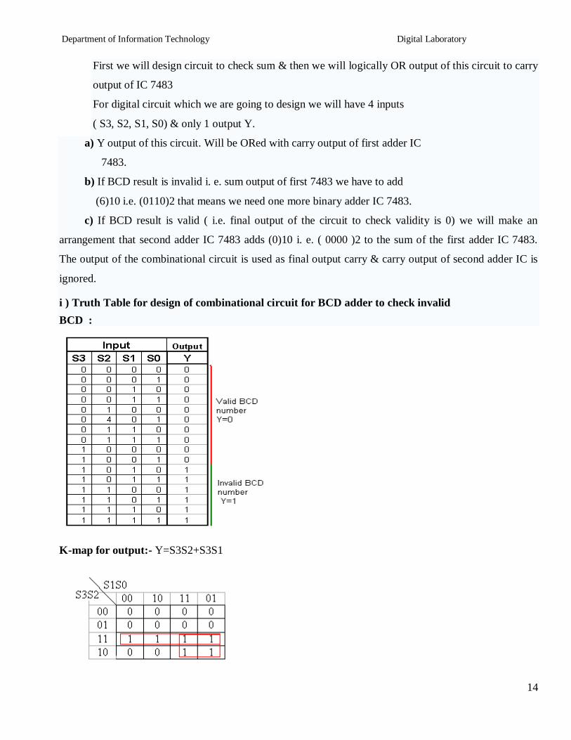
Department of Information Technology Digital Laboratory
18
Regularity Content Viva-voce Timely
Submission Total
Dated Sign of
Subject
Teacher
2 4 2 2 10
+
Date of Performance Date of Completion
-------------------------------------------------------------------------------------------------------------------
Assignment No 3
---------------------------------------------------------------------------------------------------------------------------
Title Implementation of logic functions
----------------------------------------------------------------------------------------------------------------------
Objective 1 To study the difference between multiplexer demultiplexer and decoder
2To study the applications of multiplexer
---------------------------------------------------------------------------------------------------------------------
Problem Statement Implement of Logic function using multiplexer IC 74153
---------------------------------------------------------------------------------------------------------------------
Hardware Requirement
i) IC 74153 74138 7404 7432
ii) Digital Trainer Kit -1
iii) Patch cords
----------------------------------------------------------------------------------------------------------------
Software Requirement Digital Work 30
------------------------------------------------------------------------------------------------------------------
Theory
D CWigital Multiplexer
Multiplexer are combinational digital circuits equating as controlled switches with several data inputs (I0
I1 I2 hellip) amp one single data output (ldquooutrdquo)At any time one of the Ip is transmitted to output According to
binary signals applied on control pairs to circuit Usually the number of data inputs is a power of two
Multiplexing is the process of transmitting a large no of information units over a small no of channel
digital multiplexer is a combinational large circuit which performs the operation of multiplexing It selects
Department of Information Technology Digital Laboratory
19
the operation of multiplexing It selects the operation of binary information from one of the many input
lines amp transfer to a single op line Multiplexer is called a data selector or multiposition switch because it
selects one of the many input Selection of a particular line is controlled by a set of a selection lines or
selects inputs The number of select lines depends upon no of input lines Generally there
is lsquonrsquo selects line for lsquomrsquo input lines By applying a particular code on select lines is transmitted on the
output linesBlock diagram of MUX is shown at contains lsquo2mrsquo input lines lsquomrsquo select Such that 2m = n amp
one unable input which is used to activate or dedicate MUX Depending upon the no of IP amp OP lines
various types of multiplexers are available We have 21 41 81 161 MUX Here the first no indicates
the no of input lines amp second no indicates the no of output lines
E is called as enable input which is generally active low
Fig-Block diagram for N1 Multiplxer
Demultiplexer
Demultiplexer is a logic used to perform exactly reverse function performed by multiplexer It accepts a
single input and distributes among several outputs The selection of a particular output line is controlled
by a set of selection line There are n input lines amp 2m is the number of selection line whose bit
combinations determine which output to be selected
Encoder amp Decoder
1 Encoders are used to encode given digital number into different numbering format like
decimal to BCD Encoder Octal to Binary
2 Decoders are used to decode a coded binary word like BCD to seven segment decoder
3 Thus encoder and decoder are application specific logic develop we can not use any type of
input for any encoder and decoder
Smhelliphellips1 s0
Output(Y)
D0
D1
D2
D3
Dn
N1
multiplxer
E
Department of Information Technology Digital Laboratory
20
4 Need to select input according to encoder and decoder being selected for a particular
application as mention in examples above
Uses of Mux
1 Use for Boolean function implementation
2 Construct a common bus system
3 To select between multiple sources amp signal destination
4 Inter register transfer
Advantages
1) Simplification of logic expression not required
2) Logic design is simplified
Disadvantage
Only one function can be implemented using one MUX Hence they canrsquot be used in
combinational logic circuit which contains many function
Part-A (IC 74153)
1 VERIFICATION OF IC 74153
IC 74153 is a dual layer 41 MUX It has four input lines for (I0D-I3D) for second MUX amp active high
output lsquoYarsquo lsquoYbrsquo (1Y or 2Y) It has select lines S1S0 common to both MUX The Enable inputs are
active low EaampEb(1G and 2G) The MUX is activated when they are at logic o
Pin out of IC 74153
Department of Information Technology Digital Laboratory
21
Function table of IC 74153 (X= Donrsquot Care Condition)
Select Input
Inputs (I or II) Output
S1 S0 E (I or II) D0 D1 D2 D3 Y
X X 1 X X X X 0
0 0 0 0 X X X 0
0 0 0 1 X X X 1
0 1 0 X 0 X X 0
0 1 0 X 1 X X 1
1 0 0 X X 0 X 0
1 0 0 X X 1 X 1
1 1 0 X X X 0 0
1 1 0 X X X 1 1
2CASCADING OF IC 74153
Cascading is done to expand two or more MUX ICrsquos to a digital multiplexer with larger no of inputs ie
multiplexer stocks or tress is designed The enable input is used for cascading In case of IC 74153 we
have only two select lines But for certain application 3 select lines are required then it can be
obtained by cascading using enable Now with 3 select lines we have 8 combinations Out of this
combination the MSB is O MSB is 1 for last four combination so we can use these MSB to select
any 1 MUX out of two by connecting it to E pin of first 41 MUX
Function table of IC 74153 as 8 1 Mux by cascading 2 41 Mux
Select Input Output
C (1G 2G ) B (S1) A (S0) Y
0 0 0 D0
0 0 1 D1
0 1 0 D2
0 1 1 D3
1 0 0 D4
1 0 1 D5
Department of Information Technology Digital Laboratory
22
1 1 0 D6
1 1 1 D7
3FUNCTION IMPLEMENTATION
Y= sum m (1 3 5 6)
Thisexpression is in Standard SOP form and it is three variable function So we need to use mux with
three select inputs ie 81 Mux Already we have implemented 81 Mux using IC 74153 For Boolean
function in Standard SOP form we connect data inputs corresponding to the minterms present in the given
function to Vcc and remaining data inputs to ground
Truth table
Inputs Output
C B A Y
0 0 0 0
0 0 1 1
0 1 0 0
0 1 1 1
1 0 0 0
1 0 1 1
1 1 0 1
1 1 1 0
LOGIC DIAGRAM
Hardware Requirements
GATE Quantity
IC Quantity
Mux 1 74153 1
NOT 1 7404 1
OR 1 7432 1
Department of Information Technology Digital Laboratory
23
Part-B Decoder (IC 74138)
Theory
Discrete quantities of information are requested in digital system with binary codes A binary code of n
bits is capable of representing into 2n distinct elements of the coded information
Decoder converts coded input to coded outputs accepts one of the code
There are different types of decoders such as 38 decoder 416 line decoders etc These are in general
called as n m line decoder where m=2n and n= no of input lines and m=no of output lines Demux also
takes one input data line source and selectively distributes it to one of n output channels The only
difference between demux and decoder is that demux has Din (data ip) line whereas decoder does not
have
ADVANTAGES
1) The decoder provides best implementation whenever there are many outputs of the combinational
circuit and each op of the function (or its complement) is required to be expressed with a small no
of minterms
2) The decoder can function as demux If the Enable ip line is taken as Din (data ip)
DISADVANTAGES
Since decoder method requires an OR gate for each op function so there is new hardware used And it is
always advisable to use minimum hardware as we come across problems like propagation delay of gates
APPLICATIONS
Decoder is worthily used for decoding binary information and memory interfacing It is used for the
implementation of Boolean function
Differentiate between Mux Demux Decoder
Point Multiplexer Demultiplexer Decoder
Input Many input lines Single input line Many input line also Acts as select line
Output Single output line Many output line Many output lineActive low output
Select line 2m = n n = 2m Enable inputs used
Department of Information Technology Digital Laboratory
24
A) Verification of IC 74138
We use IC 74138 which accepts 3 binary weighted inputs (A0 A1 A2) and when enabled provides
mutually exclusive active low outputs (y0-y7) It features 3 Enable ips Two active low (G2A G2B) and
one active high (G1) Every output will be high unless G2A G2Bare low and G1 is high It has
demultiplexing capability and multiple enable ips for easy expansion
IC Diagram
Function Table of 38 decoder
Input Output
Enable Data
G2A G2B G1 A2 A1 A0 Y0 Y1 Y2 Y3 Y4 Y5 Y6 Y7
0 0 0 X X X 1 1 1 1 1 1 1 1
0 1 1 X X X 1 1 1 1 1 1 1 1
1 0 1 X X X 1 1 1 1 1 1 1 1
1 1 1 X X X 1 1 1 1 1 1 1 1
Department of Information Technology Digital Laboratory
25
0 0 1 0 0 0 0 1 1 1 1 1 1 1
0 0 1 0 0 1 1 0 1 1 1 1 1 1
0 0 1 0 1 0 1 1 0 1 1 1 1 1
0 0 1 0 1 1 1 1 1 0 1 1 1 1
0 0 1 1 0 0 1 1 1 1 0 1 1 1
0 0 1 1 0 1 1 1 1 1 1 0 1 1
0 0 1 1 1 0 1 1 1 1 1 1 0 1
0 0 1 1 1 1 1 1 1 1 1 1 1 0
B) Cascading of IC 74138
The enable ip G1 active high of IC 74138 is used for cascadingfor cascading 2 ICrsquos the enable ip G1 of
first IC is connected to G1 enable ip of second IC through a NOT gate This enable ip is used as MSB
select ip line A3 the other three select input lines of both ICrsquos (A0A1A2) are also shorted to select
input lines of second IC to get single ip select lines (A0A1A2)
The ip line A3 is used to enable disable the 2 IC 74138 decoders When A3=0 first IC is enabled and
second is disabled Thus the first decoder will generate minterms from 0000 to 0111 as op and the second
decoder will generate nothing When A3=1 the enable conditions are reversed and thus second decoder
IC will generate minterms 1000 to 1111
Function Table of 416 decoder using IC 74138 (38 decoder)
Input Output
Enable Data
G2
A
G2
B
A
3
A
2
A
1
A
0
Y
0
Y
1
Y
2
Y
3
Y
4
Y
5
Y
6
Y
7
Y
8
Y
9
Y1
0
Y1
1
Y1
2
Y1
3
Y1
4
Y1
5
0 1 X X X X 1 1 1 1 1 1 1 1 1 1 1 1 1 1 1 1
Department of Information Technology Digital Laboratory
26
1 0 X X X X 1 1 1 1 1 1 1 1 1 1 1 1 1 1 1 1
1 1 X X X X 1 1 1 1 1 1 1 1 1 1 1 1 1 1 1 1
0 0 0 0 0 0 0 1 1 1 1 1 1 1 1 1 1 1 1 1 1 1
0 0 0 0 0 1 1 0 1 1 1 1 1 1 1 1 1 1 1 1 1 1
0 0 0 0 1 0 1 1 0 1 1 1 1 1 1 1 1 1 1 1 1 1
0 0 0 0 1 1 1 1 1 0 1 1 1 1 1 1 1 1 1 1 1 1
0 0 0 1 0 0 1 1 1 1 0 1 1 1 1 1 1 1 1 1 1 1
0 0 0 1 0 1 1 1 1 1 1 0 1 1 1 1 1 1 1 1 1 1
0 0 0 1 1 0 1 1 1 1 1 1 0 1 1 1 1 1 1 1 1 1
0 0 0 1 1 1 1 1 1 1 1 1 1 0 1 1 1 1 1 1 1 1
0 0 1 0 0 0 1 1 1 1 1 1 1 1 0 1 1 1 1 1 1 1
0 0 1 0 0 1 1 1 1 1 1 1 1 1 1 0 1 1 1 1 1 1
0 0 1 0 1 0 1 1 1 1 1 1 1 1 1 1 0 1 1 1 1 1
0 0 1 0 1 1 1 1 1 1 1 1 1 1 1 1 1 0 1 1 1 1
0 0 1 1 0 0 1 1 1 1 1 1 1 1 1 1 1 1 0 1 1 1
0 0 1 1 0 1 1 1 1 1 1 1 1 1 1 1 1 1 1 0 1 1
0 0 1 1 1 0 1 1 1 1 1 1 1 1 1 1 1 1 1 1 0 1
0 0 1 1 1 1 1 1 1 1 1 1 1 1 1 1 1 1 1 1 1 0
C) Implementation of Boolean function
The procedure for implementation of combinational circuit by means of a decoder and lsquoORrsquo gates requires
that the Boolean function fir the circuit be expressed in Sum of Minterms These forms can be obtained by
Department of Information Technology Digital Laboratory
27
expanding the function A decoder is then chosen which generates all the minterms of n ip variables The
ip to each OR gate are selected from the decoder outputs according to the minterms list in each function
i) F1=summ (1 3 5 7)
Truth table
Logic Diagram
ii) F2=summ (1 3 5 7111315)
Truth table
Logic Diagram
Conclusion In this way multiplexer Decoderamp its applications are studied implemented amp
tested
FAQrsquos
1What is a multiplexer
2What is a Demultiplexer
3 Enlist applications of multiplexer
Department of Information Technology Digital Laboratory
28
Regularity Content Viva-voce Timely
Submission Total
Dated Sign of
Subject
Teacher
2 4 2 2 10
Date of Performance Date of Completion
-------------------------------------------------------------------------------------------------------------------
Assignment No4
------------------------------------------------------------------------------------------------------------------
Title 3 bit updown Asynchronous and Synchronous counter using IC7476
------------------------------------------------------------------------------------------------------------------
Objective To understand design procedure of asynchronousamp Synchronous counter
------------------------------------------------------------------------------------------------------------------
Problem Statement Design (State diagram state table amp K map) and implementation of 3
bit Up and Down Asynchronous and Synchronous Counter using master slave JK flip-flop IC 7476
-----------------------------------------------------------------------------------------------------------------
Hardware Requirement
i) IC 7476 (MS-JK Flip-flop) IC 7408(Quad 2 ip AND Gate)
IC 7432 (Quad 2 ip OR Gate) and IC 7404 (Hex Inverter)
ii) Digital Trainer Kit -132
iii) Patch cords
----------------------------------------------------------------------------------------------------------------
Software Requirement Digital Work 30
------------------------------------------------------------------------------------------------------------------
Theory
Counters counters are logical device or registers capable of counting the no of states or no of clock
pulses arriving at its clock input where clock is a timing parameter arriving at regular intervals of time
so counters can be also used to measure time amp frequencies They are made up of flip flops Where the
Department of Information Technology Digital Laboratory
29
pulse are counted to be made of it goes up step by step amp the op of counter in the flip flop is decoded to
read the count to its starting step after counting n pulse incase of module counters
Types of Counters
Counter are of two types
1) Asynchronous counter
2) Synchronous counter
Asynchronous counter
A digital counter is a set of flip flop The flip flop are connected such that their combined state at any time
is binary equivalent of total no of pulses that have occurred up to that time Thus its name implies a
counter is used to count pulse A counter is used as frequency dividers To obtain waveform with
frequency that is specific fraction of clock frequency
Counter may be Asynchronous or synchronous The Asynchronous counter is also called as ripple counter
An Asynchronous counter uses T flip flop to perform a counting function The actual hardware used is
usually J-K flip flop with J amp K connected to logic1Even D flip flops may be used here
In asynchronous counter commonly called ripple counter the first flip-flop is clocked by the external
clock pulse amp then each successive flip-flop is clocked by the Q or Qrsquo output of the previous flip-flop
Therefore in an asynchronous counter the flip-floprsquos are not clocked simultaneously The input of MS-JK
is connected to VCC because when both inputs are one output is toggled As MS-JK is negative edge
triggered at each high to low transition the next flip-flop is triggered
Synchronous Counter
When counter is clocked such that each flip flop in the counter is
triggered at the same time the counter is called as synchronous counter
The gates propagation delay at reset time will not be present or we may say will not occur
1) Asynchronous Up Counter
Fig 1 shows 3bit Asynchronous Up Counter Here Flip-flop 2 act as a MSB Flip-flop and Flip-flop 0 act
as a LSB Flip-flop Clock pulse is connected to the Clock of Flip-flop 0 Output of Flip-flop 0(Q0) is
connected to clock of next flip-flop (ie Flip-flop 1) and so on As soon as clock pulse changes output is
going to change (at the negative edge of clock pulse) as a Up count sequence For 3 bit Up counter state
table is as shown below
Department of Information Technology Digital Laboratory
30
State Table
Logic diagram
Fig 1 3 Bit Asynchronous Up Counter
Hardware requirements
Gate
Flip flop
Quantity IC Quantity
MS JK 3 7476 2
2) Down Counter
Fig 2 shows 2 bit Asynchronous Down Counter Here Flip-flop 2 act as a MSB Flip-flop and Flip-flop 0
act as a LSB Flip-flop Clock pulse is connected to the Clock of Flip-flop 0 Output of Flip-flop 0 (Q0rsquo) is
Counter States Count
Q2 Q1 Q0
0 0 0 0
1 0 0 1
2 0 1 0
3 0 1 1
4 1 0 0
5 1 0 1
6 1 1 0
7 1 1 1
8 0 0 0
Department of Information Technology Digital Laboratory
31
connected to clock of next flip-flop (ie Flip-flop 1) and so on As soon as clock pulse changes output is
going to change (at the negative edge of clock pulse) as a down count sequence For 3 bit down counter
sate table is as shown below
In both the counters Inputs J and K are connected to Vcc hence J-K Flip flop work in toggle mode Preset
and Clear both are connected to logic 1
State Table
Logic diagram
Fig 2 3 Bit Asynchronous Down Counter
Hardware requirements
Counter States Count
Q2 Q1 Q0
7 1 1 1
6 1 1 0
5 1 0 1
4 1 0 0
3 0 1 1
2 0 1 0
1 0 0 1
0 0 0 0
7 1 1 1
Department of Information Technology Digital Laboratory
32
Gate
Flip flop
Quantity IC Quantity
MS JK 3 7476 2
Applications
The asynchronous counters are specially used as the counting devices
They are also used to count number of pulses applied
It also works as frequency divider
It helps in counting the number of product coming out of the machinery where product is coming out at
equal interval of time
Types of synchronous counter
1) Up counter
2) Down counter
1 3 bit Synchronous up counter
The up counter counts from 0 to7 ie(000 to 111)for this we are using MS JK flip flop In IC 74LS76 2
MS J-K flip flops are present The clock pulse is given at pin 1 amp 6 of the 1st IC amp pin 1 of 2nd IC Next
state decoder logic is designed with the help of state table
State table for synchronous up counter
Present state Next state Flip flop 3 Flip flop 2 flip flop 1
Q2 Q1 Q0 Q2 Q2 Q0 J2 K2 J1 K1 J0 K0
0 0 0 0 0 1 0 x 0 X 1 x
0 0 1 0 1 0 0 x 1 X x 1
0 1 0 0 1 1 0 x x 0 1 x
0 1 1 1 0 0 1 x x 1 x 1
1 0 0 1 0 1 x 0 0 X 1 X
1 0 1 1 1 0 x 0 1 X x 1
1 1 0 1 1 1 x 0 x 0 1 X
1 1 1 0 0 0 x 1 x 1 x 1
Department of Information Technology Digital Laboratory
33
K-Map
Q1Q0
Q2
00 01 11 10
0 0 0 1 0
1 X X X X
J2= Q1Q0
Q1Q0
Q2
00 01 11 10
0 X X X X
1 0 0 1 0
K2= Q1Q0
Q1Q0
Q2
00 01 11 10
0 0 1 X X
1 0 1 X X
J1= Q0
Q1Q0
Q2
00 01 11 10
0 X X 1 0
1 X X 1 0
K1= Q0
Department of Information Technology Digital Laboratory
34
Q1Q0
Q2
00 01 11 10
0 1 X X 1
1 1 X X 1
J0= 1
Q1Q0
Q2
00 01 11 10
0 X 1 1 X
1 X 1 1 X
K0= 1
Logic Diagram
Fig 1 3 bit Synchronous up counter
Department of Information Technology Digital Laboratory
35
2 3 bit Synchronous down counter
This is used to count from 7-0 ie(111-000)for this also 2 ICrsquos of 74LS76 are required amp hence we use 3
MS JK flip flops Here also clock is given to 1stamp 6th pin of 1st IC amp1st pin of 2nd IC enabling to apply
clock to all flip flop at a time Next state decoder logic is designed with the help of state table
State table for synchronous down counter
Present state Next state Flip flop 3 Flip flop 2 Flip flop 1
Q2 Q1 Q0 Q2 Q1 Q0 J2 K2 J1 K1 J0 K0
1 1 1 1 1 0 X 0 X 0 X 1
1 1 0 1 0 1 X 0 X 1 1 X
1 0 1 1 0 0 X 0 0 X X 1
1 0 0 0 1 1 X 1 1 X 1 X
0 1 1 0 1 0 0 X X 0 X 1
0 1 0 0 0 1 0 X X 1 1 X
0 0 1 0 0 0 0 X 0 X X 1
0 0 0 1 1 1 1 X 1 X 1 X
K-Map
Q1Q0
Q2
00 01 11 10
0 1 0 0 0
1 X X X X
J2= Q1Q0
Q1Q0
Q2
00 01 11 10
Department of Information Technology Digital Laboratory
36
0 X X X X
1 1 0 0 0
K2= Q1Q0
Q1Q0
Q2
00 01 11 10
0 1 0 X X
1 1 0 X X
J1= Q0
Q1Q0
Q2
00 01 11 10
0 X X 0 1
1 X X 0 1
K1= Q0
Q1Q0
Q2
00 01 11 10
0 1 X X 1
1 1 X X 1
J0= 1
Q1Q0
Q2
00 01 11 10
0 X 1 1 X
1 X 1 1 X
K0= 1
Department of Information Technology Digital Laboratory
37
Logic Diagram
Fig 2 3 bit Synchronous down counter
Uses
1 Specially used as the counting devices
2 Used in frequency divider circuit
3 Used in digital voltmeter
4 Used in counter type A to D converter
5 Used for time measurement
6 It helps in counting the no of product coming out from machinery where product is coming out
at equal interval of time
Conclusion
Up and down counters are successfully implemented the counters are studied amp op are checked The
state table is verified
PRACTICE ASSIGNMENTS EXERCISE MODIFICATIONS
1 Design amp implement 2 bit controlled synchronous counter
2 Designamp implement 4 bit controlled synchronous counter
3 Designamp implement truncated synchronous up or down counter
FAQrsquos with answers
1 What do you mean by Counter
A Counter is a register capable of counting the no of clock pulses arriving at its
clock inputs Count represents the no of clock pulses arrived A specified
sequence of states appears as the counter output
Department of Information Technology Digital Laboratory
38
2 What are the types of Counters Explain each
There are two types of counters as Asynchronous Counter and Synchronous Counter
Asynchronous Counter In this counter the first flip-flop is clocked by the external clock pulse
and then each successive flip-flop is clocked by the Q or Qrsquo op of the previous flip-flop Hence in
Asynchronous Counter flip-flops are not clocked simultaneously and hence called as Ripple
Counter Synchronous Counter In this counter the common clock input is connected to all the
flip-flops simultaneously
3 What do you mean by pre-settable counters
A counter in which starting state is not zero can be designed by making use of the
preset inputs of the flip flops This is referred to as loading the counter
asynchronously This is referred to as pre-settable counter
4 What are the applications of synchronous counters
Digital clock
Frequency divider circuits
Frequency counters
Used in analog to digital converters
5 What are the advantages of synchronous counters over asynchronous counters
Propagation delay time is reduced
Can operate at a much higher frequency than the asynchronous counters
6 Ring counter is an example of synchronous counters or asynchronous counter
Synchronous counter Since all the flip flops are clocked simultaneously
7 Twisted Ring (Johnsonrsquos) counter is an example of synchronous counters or asynchronous
counter
Synchronous counter Since all the flip flops are clocked simultaneously
8 What is the difference between ring counter and twisted ring counter
In ring counter pulses to be counted are applied to a counter it goes from state to state and the
output of the flip flop s in the counter is decoded to read the count Here the uncomplimentary
output (Q) of last flip flop is fed back as an input to first flip flop Ring counters are referred as
MOD lsquoNrsquo counters
Department of Information Technology Digital Laboratory
39
But in Twisted ring counter the complimentary output (Q bar) of last flip flop is fed back as an
input to first flip flop Twisted Ring counters are referred as MOD lsquo2Nrsquo counters
9 What are the applications of ring counters
Ring counter outputs are sequential non-overlapping pulses which are useful for control state
counters Used in stepper motor this requires pulses to rotate it from one position to the next Used
as divide by lsquoNrsquo ((MOD lsquoNrsquo) counters
10 What are the applications of ring counter twisted ring counters
Used as divide by lsquo2Nrsquo ((MOD lsquo2Nrsquo) counters
Used for control state counters
Used for generation of multiphase clock
11 List the Synchronous Counter ICs
IC 74160 Decade Up Counter
IC 74161 4 bit binary Up Counter
IC 74162 Decade Up Counter
IC 74163 4 bit binary Up Counter
IC 74168 Decade UpDown Counter
IC 74169 4 bit Binary UpDown Counter
IC 74190 Decade UpDown Counter
IC 74191 4 bit Binary UpDown Counter
IC 74192 Decade UpDown Counter
IC 74193 4 bit Binary UpDown Counter
Department of Information Technology Digital Laboratory
40
Regularity Content Viva-voce Timely
Submission Total
Dated Sign of
Subject
Teacher
2 4 2 2 10
Date of Performance Date of Completion
-------------------------------------------------------------------------------------------------------------------
Assignment No 5
-------------------------------------------------------------------------------------------------------------------------------
Title Design and implementation of Module lsquonrsquo counter with IC7490 and IC 74191
-----------------------------------------------------------------------------------------------------------------------------
Objective To know difference between regular amp truncated counter as well as binary ampBCD Counter
--------------------------------------------------------------------------------------------------------------------------------
Problem Statement To design and implement mod - 10 mod ndash 7 mod - 99 asynchronous BCD
counter using IC 7490 and to design and implement up down mod - n Binary counter using IC 74191
-----------------------------------------------------------------------------------------------------------------
Hardware Requirement
i) IC 7490 IC 74191 basic gates
ii) Digital Trainer Kit -1
iii) Patch cords
----------------------------------------------------------------------------------------------------------------
Software Requirement Digital Work 30
------------------------------------------------------------------------------------------------------------------
Theory
Part A ndash IC 7490
IC 7490 is a TTL MSI (medium scale integration) decade counter It contains 4 master slave flip flops
internally connected to provide MOD-2 ie divide by 2 and MOD-5 ie divide by 5 counters MOD-2 and
Mod-5 counters can be used independently or in cascading
Department of Information Technology Digital Laboratory
41
It is a 4-bit ripple type decade counter The device consists of 4-master slave flip flops internally
connected to provide a divide by two and divide by 5 sections Each section has a separate clock ip to
initiate state changes of the counter on the high to low clock transition
Since the op from the divide by 2 section is not internally connected to the succeeding stages The device
may be operated in various counting modes In a BCD counter the CP1 input must be externally connected
to QA op The CP0ip receives the incoming count producing a BCD count sequence It is also provided
with additional gating to provide a divide by 2 counter and binary counter for which the count cycle length
is divide by 5 The device may be operated in various counting modes
There are 2 reset inputs R0(1) and R0(2) both of which need to be connected to the lsquologic 1rsquo for clearing all
flip flops Two set inputs Rg(1) and Rg(2) when connected to logic 1 are used for setting counter to 1001
(BCD 9)
Pin out of IC 7490
Fig Pin configuration of IC7490
Table 1-pin name and description of IC7490
Pin name Description
Input B This is clock input to the internal MOD-5 ripple counter which is negative
edge triggered
R0(1)R0(2) Gated zero reset inputs
Department of Information Technology Digital Laboratory
42
R9(1)R9(2) These are gated set to nine inputs
QDQCQB Output of internal MOD-5 counter with QD as MSB
QA Output of internal MOD-2 counter with QA as LSB
Input A Clock input to FF-A which is negative edge triggered
Functional Table for IC7490
Reset inputs Output
R0(1) R0(2) R9(0) R9(1) QD QC QB QA
1 1 0 X 0 0 0 0
1 1 X 0 0 0 0 0
X X 1 1 1 0 0 1
X 0 X 0 COUNTER
0 X 0 X COUNTER
0 X X 0 COUNTER
X 0 0 x COUNTER
Department of Information Technology Digital Laboratory
43
Basic internal Structure of IC 7490
Function Table of MOD-5 counter
Design of MOD-10 counter using IC 7490
The QA op the first flip flop is connected to the input B which is clock ip of internal MOD-5 ripple
counter Due to cascading of Mod-2 and Mod-5 counters the overall configuration the decade counters
count from 0000 to 1001 After 1001 mod-5 resets to 0000 and next count after 1001 is 0000
When QA op is connected to B ip we have the Mod-2 counter followed by Mod-5 counter The
count sequence obtained is shown in the table It may be noted that QA changes from 0 to 1 the state of
InputB clock Output
Count QD QC QB
0 0 0 0
0 0 1 1
0 1 0 2
0 1 1 3
1 0 0 4
Department of Information Technology Digital Laboratory
44
Mod-5 counter doesnrsquot change whereas when QA changes from 1 to 0 the Mod-5 counter goes to the next
state
Logic DiagramMOD-10 counter using IC 7490
5 Modulus n Counter
Function table
Ip clock
Output
Count QD QC QB QA
0 0 0 0 0
0 0 0 1 1
0 0 1 0 2
0 0 1 1 3
0 1 0 0 4
Department of Information Technology Digital Laboratory
45
Design of Mod-7 Counter using IC 7490
Mod-7 counter counts through seven states from 0 to 6 counters and it should reset as soon as the
count becomes 7 The op of reset logic should be 1 corresponding to invalid states The reset logic op
should be applied to pin 2 and 3
Truth Table of Reset Logic
0 1 0 1 5
0 1 1 0 6
0 1 1 1 7
1 0 0 0 8
1 0 0 1 9
QD QC QB QA Y
0 0 0 0 0
0 0 0 1 0
0 0 1 0 0
0 0 1 1 0
0 1 0 0 0
0 1 0 1 0
0 1 1 0 0
0 1 1 1 1
1 0 0 0 1
1 0 0 1 1
Department of Information Technology Digital Laboratory
46
Logic Diagram Mod 7 Counter using IC 7490
Function table
Ip clock
Output
Count QD QC QB QA
0 0 0 0 0
0 0 0 1 1
0 0 1 0 2
0 0 1 1 3
0 1 0 0 4
0 1 0 1 5
0 1 1 0 6
Department of Information Technology Digital Laboratory
47
Design of Mod-99 using IC 7490
For Mod-99 two IC 7490rsquos will be required Hence to implement a divide by 99 counter we have
to use two decade counters ICrsquos A divide by 99 counter counts 99 states from 0 to 98 and the counter
should reset as soon as the count becomes 99 So in order to reset the counter of 99 connect the Q op
which are equal to 1 in the count of 99 to an lsquoAndrsquo gate amp then connect and op to the reset ip of both
ICrsquos
MOD-100 Counter-
MOD-100 counter can be obtained by cascading two decade counter ICrsquos
Each IC gives divide by 10 counts Hence 2 ICs will give 1010=100 counts
Clock is applied to the input A of IC 7490 the Q1 output is connected to B input etc
For cascading the QD output of the first IC is connected to the input A of second IC Thus QD of
IC-(1) acts as clock input to IC-(2)
The Ro (1) Ro(2) R9(1) R9(2) inputs of both ICs are connected to ground so as to make them
inactive
The total count provided by the two counters varies from 00 to 99 decimal that means 100 states
Hence it is a MOD-10 counter
Impleacutementations
FigureMOD-100 counters using IC 7490
Department of Information Technology Digital Laboratory
48
B) IC 74191 ndash Theory
IC74191 is 4-bit binary synchronous reversible up down counter It contains 4 master slave flip flops
with internal gating and steering logic to provide asynchronous reset and synchronous count updown
operations its asynchronous parallel capability permits the counter to be preset to any desire number D0
to D3 are the parallel data inputs Information present on the parallel data inputs D0 to D3 is loaded into
the counter and appears on the output when the load PLinput is lowThisoperation overrides the counting
function Counting is inhabited by the high level on the enable G input when G input is low internal state
changes are initiated synchronously by the low to high transitions of the clock inputs the updown input
signal determines the direction of input
Function Table
Operating
mode
Inputs Outputs
PL UD G CLK Dn
Parallel
load L X X X L L
L X X X H H
Count up H L 0 uarr X Count up
Count
down H H 0 uarr X
Count
down
Hold(No
change) H X H X X No change
Pin details ndash
D0 to D3 input lines PL parallel load
G is Enable input ndash enabling the counting
Q0 to Q3 output lines
Downup determines the direction of counting
Clk clock input for counter
Terminal Count Max(1111) min(0000) For these states signal goes high for 1clock pulse
Ripple clock Clock input for next higher state
Department of Information Technology Digital Laboratory
49
Pin Diagram IC 74191
Up counter- Truth Table
Clk
Pulses QA QB QC QD
0 0 0 0 0
1 0 0 0 1
2 0 0 1 0
3 0 0 1 1
4 0 1 0 0
5 0 1 0 1
6 0 1 1 0
7 1 1 1 1
8 1 0 0 0
9 1 0 0 1
10 1 0 1 0
11 1 0 1 1
12 1 1 0 0
13 1 1 0 1
Department of Information Technology Digital Laboratory
50
14 1 1 1 0
15 1 1 1 1
Logic Diagram
Steps-
Connect the circuit as shown above
Apply clock ip to pin no14
Connect UD to GND
Verify the output according to truth table
Logic diagram of down counter
Steps-
Connect the circuit as shown above
Apply clock ip to pin no14
Connect UD to VCC
Verify the output according to truth table
UD D3 D2 D1 D0 PL
Clock IC 74191
G RC
MAX MIN
Q3 Q2 Q1 Q0 TC
vcc
NC
NC
Outputs
no connection
vcc
Department of Information Technology Digital Laboratory
51
With the help of IC74191 we can implement truncated updown counter by using following logic ndash
Connect data input line to particular count you want to load
According to requirement make Truth table
Draw the K-map
Find out Boolean expression
Draw the logic diagram and that is the combinational logic for your count and apply the output of
that circuit to PL
According to requirement we get the UP and down counting
5 Modulus n Counter
Presettable updown counter
Mod 11 counter
Implementation of presetttable mod updown counter using IC- 74LS191
1 Load Data on data lines D0 to D3 (0101)
2 Counter will go through the states from 0101 0110hellip1111 in up counter and 0101 to 0000 in
down counter
Combinational Circuit
CLOCK D3 D2 D1 D0
TC
U D 74191 RC
G PL
Updown Q3 Q2 Q1 Q0 PL
Q3 Q2 Q1 Q0
Preset Count
Department of Information Technology Digital Laboratory
52
3 The logic circuit should be designed in such a way that only when all the outputs are high output
of the reset circuit should be low and the counter should jump to state 5 It should again start
counting from 0101 to 0000
State Table
Down Counter UP Counter
IC 74191 is 4 bit counter Thus it counts 0000 to 1111 different 16 states For MOD11 counter we require
different 11 states so 5 steps must be skipped from 16 states We get MOD11 by presetting counter to
value 5
Assignment Question
Design and Implement MOD 7 MOD 10 and MOD 12 using IC 74191
FAQs
1 What do you mean modulus counter
Counter
state Clock
pulse
Q3 Q2 Q1 Q0
1 0 1 0 1
2 0 1 1 0
3 0 1 1 1
4 1 0 0 0
5 1 0 0 1
6 1 0 1 0
7 1 0 1 1
8 1 1 0 0
9 1 1 0 1
10 1 1 1 1
11 1 1 1 1
Counter state
Clock pulse
FF outputs
Q3 Q2 Q1 Q0
1 0 1 0 1
2 0 1 0 0
3 0 0 1 1
4 0 0 1 0
5 0 0 0 1
6 0 0 0 0
7 0 1 0 1
Department of Information Technology Digital Laboratory
53
It represents the number of possible states of counter
2 How will you use the 7490 IC to design symmetrical divide by 10 frequency counter
The divide by 5 circuit followed by divide by 2 circuit will give symmetrical output
3Where counters are used Give real life example of counter
Modulus n Counter
Binary counter ndash An N stage counter that recycles after 2 Ncount The count proceds in specified binary
sequence Counter Presetable- A counter which can be set to a desired value before the start of the
counting UPDown counter ndash A counter that can count in both up and down direction depending upon a
control input
Department of Information Technology Digital Laboratory
54
Regularity Content Viva-voce Timely
Submission Total
Dated Sign of
Subject
Teacher
2 4 2 2 10
Date of Performance Date of Completion
-------------------------------------------------------------------------------------------------------------------
Assignment No6
------------------------------------------------------------------------------------------------------------------
Title Sequence Generator
------------------------------------------------------------------------------------------------------------------
Objective To understand sequence generator one of the sequential circuit
-------------------------------------------------------------------------------------------------------------------
Problem Statement Design (State Diagram State Table K Map) and implementation of Sequence
Generator using Shift Register IC 74194
-----------------------------------------------------------------------------------------------------------------
Hardware Requirement
i) IC 741947408 (AND-gate) 7432 (OR-gate)
ii) Digital Trainer Kit -1
iii) Patch cords
----------------------------------------------------------------------------------------------------------------
Software Requirement Digital Work 30
------------------------------------------------------------------------------------------------------------------
Theory
Part A Sequence Generator with Flip flop
A sequential circuit which generates a prescribed sequence of bits in synchronism with a clock is referred
to as a sequence generator These pulse trains or sequence of bits can be used to open valves close gates
turn on lights and turn off machines and other variety of jobs
Department of Information Technology Digital Laboratory
55
For the design of sequence generator we first determine the required no of flip flops and the logic circuit
for the next state decoder
No of flip flops required to generate particular sequence can be determined as follows
1) Find the no of 1rsquos in the sequence
2) Find the no of 0rsquos in the sequence
3) Take the maximum out of two
4) If N is the required no of flip flops choose minimum value of lsquonrsquo to satisfy equation given below
Max (0rsquos 1rsquos) le 2n-1
The sequence generator can be classified as
1) sequence generator without bushing
2) sequence generator with bushing
The aim in this experiment is to design a sequence generator to generate a sequence of bit ie 10101
Part B Sequence Generator using Shift Register IC 74194
IC 74194 4 bit bidirectional Shift Register
This bidirectional shift register is designed to incorporate virtually all the features a system designer may
want in a shift register they feature Parallel inputs parallel outputs right shift left shift serialinputs
operating mode control inputsand a direct overriding clear line The register has four distinct modes of
operationsnamely
1 Parallel load
2 Shift right (in the direction QA towards QD)
3 Shift left (in the direction QD towards QA)
4 Inhibit clock (do nothing)
Synchronous parallel loading is accomplished by applying the four bits of data and taking both
mode control inputs S0 and S1High The data is loaded in to the associated flip-flops and appear
at the outputs after positive transition of the clock input During loading serial data flow is
inhibited
Shift right is accomplished synchronously with the rising edge of the clock pulse when S0 is High
and S1 is Low Serial data for this mode is entered at the shift right data input When S0 is Low
and S1 is High data shifts left synchronously and new data is entered at the shift left serial input
Clocking of the flip flop is inhibited when both mode control inputs are LOW
Department of Information Technology Digital Laboratory
56
Mode Control Input Operation
S1 S0
0 0 Clock Inhibit
0 1 Shift right
1 0 Shift Left
1 1 Parallel loading
Function Table of IC 74194
Design
The minimum number of flip-flops N required to generate a sequence of length S is given by S
le 2N ndash 1
In this case S=7 therefore the minimum value of N which may generate in this sequence is 3
However it is not guaranteed to lead to a solution If the given sequence leads to seven distinct
states then only three flip flops are sufficient otherwise we have to increase the number of flip
flops We write the states of circuit as given in table 1 The prescribed sequence is listed under QA
and the sequence listed under QB and QC are the same sequence delayed by one and two clock
pulses respectively From the table we observe that all the states are not distinct which means N=3
is not sufficient Next we assume that N=4 and prepare table 2 The last column gives the required
serial input for getting the desired change of state when a clock pulse is applied This is obtained
by assuming D type flip flop and looking at the QA output For example at the falling edge of first
clock pulse QA=1 The second clock pulse must result in QA=1 which requires its D input to be 1
In the same manner all the entries in column Y are determined
Table 1 State Assignment Table of Sequence Generator (N=3)
Number of Clock
Pulses
Flip Flop Inputs States
QA QB QC
1 1 1 1 7
2 1 1 1 7
3 0 1 1 3
4 1 0 1 5
Department of Information Technology Digital Laboratory
57
5 0 1 0 2
6 1 0 1 5
7 1 1 0 6
Excitation table of D Flip-Flop
Present State Qn Next State Qn+1 Flip-Flop Input D
0 0 0
0 1 1
1 0 0
1 1 1
Table 2State Assignment Table of Sequence Generator (N=4)
Number of Clock
Pulses
Flip Flop Inputs States
Y
Serial ip QA QB QC QD
1 1 1 1 0 14 1
2 1 1 1 1 15 0
3 0 1 1 1 7 1
4 1 0 1 1 11 0
5 0 1 0 1 5 1
6 1 0 1 0 10 1
7 1 1 0 1 13 1
K-Map Simplification
Department of Information Technology Digital Laboratory
58
00 01 11 10
00 X X X X
01 X 1 1 X
11 X 1 0 1
10 X X 0 1
Y= QArsquo + QBrsquo + QCrsquo = QAQBQC
LOGIC DIAGRAM
HARDWARE REQUIREMENTS
Sr no ICs Description Quantity
11 74194 4 bit bidirectional universal shift register 16ktr`
2 7410 3 input NAND Gate 1
Department of Information Technology Digital Laboratory
59
Conclusion In this way sequence generator using JK flip flips amp shift register is designed and
implemented
Enhancements Modifications ndash Sequence generator can also be implemented with shift register instead
of flip flops Use IC 7495 universal shift register IC and try to implement sequence generator
FAQs
1 What is sequential logic circuit
A sequential logic circuit consists of a memory elements in addition to
combinational circuit Its output at any instant of time depends upon
the present input as well as present state of memory element
2 What is meant by delay line
It is used to introduce time delays in digital signals
3 What is meant by following terms
a) Synchronous preset b) Asynchronous preset
c) Synchronous clear d) Asynchronous clear
a)Preset operation is synchronised with the clock
b)Preset operation is independent of the clock
c) clear is performed in synchronous with clock
d) clear is performed independent with clock
4 Is asynchronous counter faster than synchronous counter
In a synchronous counter the time required for change of any state is same and is equal to delay
time of one flip flop where as in asynchronous counter all flip flops are not clocked
simultaneously hence time required is not same
5 What is mean by lockout in counter
In a counter design for a fewer state than the maximum possible state some time it may so happen
that counter enters in unused state and goes from one unused state to another unused state and
never comes to used state
6 What is mean by state table
Department of Information Technology Digital Laboratory
60
It consists of complete information about present state and next state and outputs of a sequential
system
7 What is mean by state diagram
The information available in a state table can be represented as graphically the graphical
representation is known as state diagram
8 What is the advantage of state reduction in the design of sequential circuit
It reduces the number of flip flops
9 What is meant by excitation table
This gives information about what should be the flip flop inputs if outputs are specified before and
after the clock pulse
10 How many flip flops are required to design sequence generator using Counters
max (0rsquoS1rsquoS) in a given sequence lt= 2(N - 1)
Where N = Number of flip flops
11 How many flip flops are required to design sequence generator using shift registers
Slt= 2N - 1
Where N=Number of flip flops
S= Length of sequence
12 What is Lock out condition How it is avoided
When counter enters into one of the invalid state and after application of pulses remains in invalid
states only i e counter gets locked into invalid state amp this is called as lock out Lock out can be
avoided by providing bushing to all the invalid states in such a way that after application of one or
more clock pulses counter will fall into one of the valid state
Department of Information Technology Digital Laboratory
61
Regularity Content Viva-voce Timely
Submission Total
Dated Sign of
Subject
Teacher
2 4 2 2 10
Date of Performance Date of Completion
-------------------------------------------------------------------------------------------------------------------
Assignment No7
------------------------------------------------------------------------------------------------------------------
Title Multiplexer using Data flow modeling and structural modeling
------------------------------------------------------------------------------------------------------------------
Objective To learn data flow modeling style Its uses and different types of declarations with some
different types of circuits Structure of VHDL program is well discussed with this modeling style
-------------------------------------------------------------------------------------------------------------------
Problem Statement 41 multiplexer using data flow amp structural modeling -
----------------------------------------------------------------------------------------------------------------
Hardware Requirement - NA
----------------------------------------------------------------------------------------------------------------
Software Requirement Xilinx
------------------------------------------------------------------------------------------------------------------
Theory
Data flow style-
In this type of design the view of data as flowing from input to output through a design
An operation is defined in terms of a collection of data transformation expressed as concurrent
statement Each of the statement can be activated when any of its input signal changes its value While
these statements describe the behavior of the circuit a lot of information about its structure can be
extracted from the description as well
Data flow modeling has a set of concurrent assignment statements In the data flow level of abstraction we
describe how information is passed in the circuit The built in operators in VHDL are used in expression
such as AND OR XOR NOT etc
Department of Information Technology Digital Laboratory
62
INPUT
Two select lines S1S0
Four data lines D0 D1 D2 D3
OUTPUT
One output line Y
Functional block diagram of 41 Mux
Fig 41 Multiplexer using Data flow modeling
Function table of 41 Mux
Enable S1 S0 A B C D Y
1 X X X X X X 0
0 0 0 A X X X A
0 0 1 X B X X B
0 1 0 X X C X C
0 1 1 X X X D D
Design steps
Click on Xilinx ISE 92i
Create New project from file menu Ensure top level source is HDL
Select family of devices (usually spartan2E or 3)
Department of Information Technology Digital Laboratory
63
Ensure preferred language is VHDL
Click new source which shows you project details device details
and Synthesis and simulator tools
After finishing project create new source by right clicking in project name with VHDL
module
Complete ports name directions and bus Ensure architecture name is behavioral
After that we will get design summary and detailed reports
Close design summary
Create your code with given modeling style
Go to process window and synthesis to check if any error is there in code Check syntax and
view RTL schematic
Create new source to simulate the code
Right click on source name and create test bench waveform with proper name Ensure the
project is same
Click on combinational circuit in initial timing wizard
Select test bench wave in source window Apply inputs to wave diagram Ensure you are in
behavioral simulation
Go to process box Click on Xilinx ISE simulator and simulate the model See results
RTL Schematic
Department of Information Technology Digital Laboratory
64
Timing Diagram
FAQrsquos
1 What are the different kinds of data objects in VHDL code
Ans data object may be any value or number still some signal data objects and bit and bit_vector
types of these are available in VHDL STD_LOGIC and STD_LOGIC_VECTOR types are used
widely in programming
2 What do you mean by signal
Ans signal is a data object represents logic signals or wires in a circuit There are three places in
which signals can be declared in VHDL code in an entity declaration in the declarative section of
architecture and in declarative section of package
3 What are different signal types
Ans BIT BIT_VECTOR STD_LOGIC STD_LOGIC_VECTOR STD_ULOGIC SIGNED
UNSIGNED INTEGER ENUMERATION and BOOLEAN
4 What is an entity
Ans a circuit or sub circuit described with VHDL code is called a design entity
5 Explain structure of an entity
Ans it has two main parts the entity declaration which specifies the input and output signals for
entity and the architecture which gives circuit details
Department of Information Technology Digital Laboratory
65
6 How will you declare a package with component Explain structure
The general form of package declaration is as shown in diagram
PACKAGE package_name IS
[TYPE declarations]
[SIGNAL declarations]
[COMPONENT declarations]
END package_name
Entity
Declaration Architecture
Department of Information Technology Digital Laboratory
66
Regularity Content Viva-voce Timely
Submission Total
Dated Sign of
Subject
Teacher
2 4 2 2 10
Date of Performance Date of Completion
-------------------------------------------------------------------------------------------------------------------
Assignment No8
------------------------------------------------------------------------------------------------------------------
Title Full Adder using Behavioral and Structural modeling
------------------------------------------------------------------------------------------------------------------
Objective To learn structural modeling style Its uses and different types of declarations with some
different types of circuits Structure of VHDL program is well discussed with this modeling style
-------------------------------------------------------------------------------------------------------------------
Problem Statement Full adder using behavioral amp structural modeling
-----------------------------------------------------------------------------------------------------------------
Hardware Requirement - NA
----------------------------------------------------------------------------------------------------------------
Software Requirement Xilinx
------------------------------------------------------------------------------------------------------------------
Theory
Structural style-
A digital electronic system can be described as a module with inputs andor outputs The electrical values
on the outputs are same functions of the values of inputs The example of it is as shown The NAND gate
has 2ips AampB amp an output y Using VHDL terminology we call the NAND2 design entity amp the inputs
amp outputs are called ports 1 way of describing the function of NAND2 is to describe how it is composed
of sub modules AND amp INVERTER Each of the Sub modules is an instance of some entity amp ports of the
instances are connected using signals Structural modeling has a set of interconnected component
Structure can be used to create a very low level description of a circuit or a very high level description
Department of Information Technology Digital Laboratory
67
In a gate level description of a circuit for example components such as basic logic gates amp FFs might be
connected in some logical stricture to create the circuit This is what is often called a net list
Structure of structural modeling
Functional block diagram of Full Adder
architectureNetlistofHalf_Adderis
-- component with locals
componentMyXorport (A_XorB_Xor in BIT
Z_Xor out BIT)
end component
-- component with locals
componentMyAndport (A_AndB_And in BIT
Z_And out BIT)
end component
begin
Xor1 MyXorport map (X Y Sum)
-- instance with actuals
And1 MyAndport map (X Y Cout)
-- instance with actuals
end
Department of Information Technology Digital Laboratory
68
Function table of Full Adder
A B Cin SUM CARRY
0 0 0 0 0
0 0 1 1 0
0 1 0 1 0
0 1 1 0 1
1 0 0 1 0
1 0 1 0 1
1 1 0 0 1
1 1 1 1 1
Sum = Σm(1 2 4 7)
Carry= Σm(3 5 6 7)
Design steps
Click on Xilinx ISE 92i
Create New project from file menu Ensure top level source is HDL
Select family of devices (usually spartan2E or 3)
Ensure preferred language is VHDL
Click new source which shows you project details device details
and Synthesis and simulator tools
After finishing project create new source(full adder) by right clicking in project name with
VHDL module
Complete ports name directions and bus Ensure architecture name is behavioral
After that we will get design summary and detailed reports
Close design summary
Click new source which shows you project details device details
and Synthesis and simulator tools
After finishing project create new source(half adder) by right clicking in project name with
VHDL module
Complete ports name directions and bus Ensure architecture name is behavioral Names
should be same as previous inputs
Department of Information Technology Digital Laboratory
69
After that we will get design summary and detailed reports
Close design summary
Create your code for half adder with given modeling style
After that go to process window Click on design utilities
View HDL instantiation code of half adder
Copy component part of half adder in architecture block of full adder Copy instantiation
template twice after begin as we require two half adders to construct full adder (structural
modeling) Name them differently (eg ha1 or ha2)
Create signals as per the logic Complete code of full adder
Go to process window and synthesis to check if any error is there in code Check syntax and
view RTL schematic
Create new source to simulate the code
Right click on source name and create test bench waveform with proper name Ensure the
project is same
Click on combinational circuit in initial timing wizard
Select test bench wave in source window Apply inputs to wave diagram Ensure you are in
behavioral simulation
Go to process box Click on Xilinx ISE simulator and simulate the model See results
RTL Schematic
Timing Diagram
Department of Information Technology Digital Laboratory
70
INPUT
Three inputs A B Carry (previous)
OUTPUT
Two outputs Sum Carry
FAQrsquos
1 What do you mean by structural style
Ans in this type of code a circuit is described in hierarchical fashion by connecting together sub
circuits
2 Explain IF statement with example
Ans The general form of an IF statement is as follws
IF Sel=rsquo0rsquo THEN
Flt=x1
ELSE
Flt=x2
END IF
Department of Information Technology Digital Laboratory
71
3 Explain declaration and instantiation process in VHDL
Ans first declare a small vhdl code in formal way Eg half adder Define project name is full adder
And simply copy instantiation template in main source code Define how many times you want to
declare this template Give separate names for those
4 What is STD_LOGIC_VECTOR
Ans It is standard data object added to VHDL standard in IEEE 1164 It provides more flexibility
than the Bit type
5 Explain difference between concurrent and sequential statements
Ans Concurrent statements define interconnected processes and blocks that together describe a designrsquos
overall behavior or structure They can be grouped using block sstatement Groups of blocks can also be
partitioned into other blocks At this same level a VHDL component can be connected to define signals
within the blocks
It is a reference to an entity A process can be a single signal assignment statement or a series of
sequential statements (SS) Within a process procedures and functions can partition the sequential
statements
PRACTICE ASSIGNMENTS
1 Implement half adder using data flow modeling
2 Implement Full Adder using behavioral modeling
3 Implement 3 bit magnitude comparator using a 3 bit adder
4 Implement half sub tractor using data flow modeling
5 Write VHDL code for Full Subtractor
Department of Information Technology Digital Laboratory
72
Regularity Content Viva-voce Timely
Submission Total
Dated Sign of
Subject
Teacher
2 4 2 2 10
rsquozaDate of Performance Date of Completion
-------------------------------------------------------------------------------------------------------------------
Assignment No9
------------------------------------------------------------------------------------------------------------------
Title Simulation of 3 bit Connter using Behavioral modeling
------------------------------------------------------------------------------------------------------------------
Objective To learn behavioral modeling style Its uses and different types of declarations with some
different types of circuits Structure of VHDL program is well discussed with this modeling style
-------------------------------------------------------------------------------------------------------------------
Problem Statement 3 bit controlled up down synchronous counter with preset amp clear
-----------------------------------------------------------------------------------------------------------------
Hardware Requirement -NA
----------------------------------------------------------------------------------------------------------------
Software Requirement Xilinx
------------------------------------------------------------------------------------------------------------------
Theory
Behavioral style-
Highest level of abstraction supported in VHDL is called the behavior level of abstraction In it we have
for loop while loop If then else case ampvariable assignment The statements are enclosed in a PROCESS
block amp are executed sequentially
In it circuit is described in terms of its operation overtime
In behavioral description the concept of time may be expressed precisely with actual delays between
related events (such as the propagation delays within gates amp on wires) or it may be simply an ordering of
operation that are expressed sequentially (such as in a functional description of a FF)
Department of Information Technology Digital Laboratory
73
A behavioral design method defines a circuit in terms of text language rather than a schematic of
interconnected symbols
Behavioral design is a technology independent text based design that incorporates high level
functionality amp high level information flow
Structure of Behavioral modeling
Functional block diagram of 3 bit controlled up down synchronous counter with preset amp clear
Function table of 3 bit controlled up down synchronous counter with preset amp clear
Design steps
Click on Xilinx ISE 92i
Create New project from file menu Ensure top level source is HDL
Select family of devices (usually spartan2E or 3)
Ensure preferred language is VHDL
Click new source which shows you project details device details
and Synthesis and simulator tools
After finishing project create new source by right clicking in project name with VHDL
module
Complete ports name directions and bus Ensure architecture name is behavioral
After that we will get design summary and detailed reports
Close design summary
Create your code with given modeling style
Go to process window and synthesis to check if any error is there in code Check syntax
and view RTL schematic Create new source to simulate the code
Department of Information Technology Digital Laboratory
74
Right click on source name and create test bench waveform with proper name Ensure the
project is same
Click on combinational circuit in initial timing wizard
Select test bench wave in source window Apply inputs to wave diagram Ensure you are in
behavioral simulation
Go to process box Click on Xilinx ISE simulator and simulate the model
RTL Schematic
Timing Diagram
INPUT
Clock Preset Clear
OUTPUT
Three output lines
FAQrsquos
1 Explain the structure of behavioral modeling
2 What are the differences between behavioral and structural modeling
Ans Behavioral descriptionof a circuit is the highest level of abstraction in VHDL Here the
circuit is described in terms of it operation with respect to time All operations are in one level of
code The operations are described in a way that the designer of a sequential circuit infers a
register
Structural description on the other hand is a circuit description in terms of its components
it can either create a low level description much like a hierarchy in a block diagram Whenever
you see a component instantiated in a code that code employs structural description of the circuit
The components are connected in the form of a netlist This is for better manageability and
reusability
3 What are the differences between behavioral and data flow modeling
Department of Information Technology Digital Laboratory
75
Ans Behavioral ndash describes how the output is derived from the inputs using structured
statements
Dataflow ndash describes how the data flows from the inputs to the output most often
using NOT AND and OR operations
4 What do you mean by process statement
Ans The process statement begins with the PROCESS keyword followed by a parenthesized list
of signals called the sensitivity list It operates on selected and conditional statements
5 Explain syntax of process statement
Ans BEGIN
Process( sensitivity list)
END process
PRACTICE ASSIGNMENTS
1 Implement 3 bit asynchronous up counter using behavioral modeling
2 Implement 3 bit asynchronous down counter using behavioral modeling
3 Implement 3 bit synchronous down counter using behavioral modeling
End
Department of Information Technology Digital Laboratory
76
Pin Diagrams
7400 Quad 2-Input NAND Gate
7402 Quad 2-Input NOR Gate
7404 Not Gates
7408 Quad 2-Input AND Gates
7432 Quad 2-Input OR Gate
7486 Quad 2-Input Exclusive-OR Gate
Department of Information Technology Digital Laboratory
77
7483 4 bit Binary Adder
7490 Decade and Binary Counters
74138 38 Decoder
Department of Information Technology Digital Laboratory
78
74153 Dual 41 Multiplexer
74191 Synchronous UpDown 4 bit Binary counter with Mode Control
Department of Information Technology Digital Laboratory
79
74194 Universal Shift Register
7476 Dual Master-Slave J-K Flip-Flops
- Part B Sequence Generator using Shift Register IC 74194
-
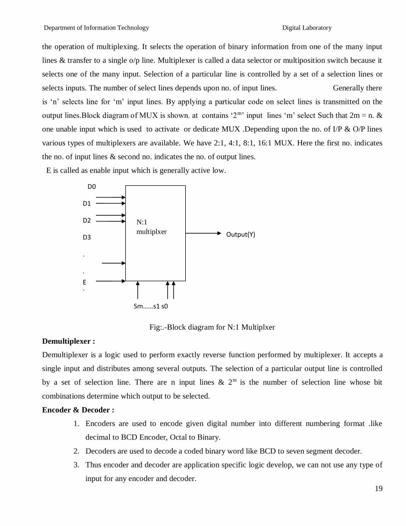
Department of Information Technology Digital Laboratory
20
4 Need to select input according to encoder and decoder being selected for a particular
application as mention in examples above
Uses of Mux
1 Use for Boolean function implementation
2 Construct a common bus system
3 To select between multiple sources amp signal destination
4 Inter register transfer
Advantages
1) Simplification of logic expression not required
2) Logic design is simplified
Disadvantage
Only one function can be implemented using one MUX Hence they canrsquot be used in
combinational logic circuit which contains many function
Part-A (IC 74153)
1 VERIFICATION OF IC 74153
IC 74153 is a dual layer 41 MUX It has four input lines for (I0D-I3D) for second MUX amp active high
output lsquoYarsquo lsquoYbrsquo (1Y or 2Y) It has select lines S1S0 common to both MUX The Enable inputs are
active low EaampEb(1G and 2G) The MUX is activated when they are at logic o
Pin out of IC 74153
Department of Information Technology Digital Laboratory
21
Function table of IC 74153 (X= Donrsquot Care Condition)
Select Input
Inputs (I or II) Output
S1 S0 E (I or II) D0 D1 D2 D3 Y
X X 1 X X X X 0
0 0 0 0 X X X 0
0 0 0 1 X X X 1
0 1 0 X 0 X X 0
0 1 0 X 1 X X 1
1 0 0 X X 0 X 0
1 0 0 X X 1 X 1
1 1 0 X X X 0 0
1 1 0 X X X 1 1
2CASCADING OF IC 74153
Cascading is done to expand two or more MUX ICrsquos to a digital multiplexer with larger no of inputs ie
multiplexer stocks or tress is designed The enable input is used for cascading In case of IC 74153 we
have only two select lines But for certain application 3 select lines are required then it can be
obtained by cascading using enable Now with 3 select lines we have 8 combinations Out of this
combination the MSB is O MSB is 1 for last four combination so we can use these MSB to select
any 1 MUX out of two by connecting it to E pin of first 41 MUX
Function table of IC 74153 as 8 1 Mux by cascading 2 41 Mux
Select Input Output
C (1G 2G ) B (S1) A (S0) Y
0 0 0 D0
0 0 1 D1
0 1 0 D2
0 1 1 D3
1 0 0 D4
1 0 1 D5
Department of Information Technology Digital Laboratory
22
1 1 0 D6
1 1 1 D7
3FUNCTION IMPLEMENTATION
Y= sum m (1 3 5 6)
Thisexpression is in Standard SOP form and it is three variable function So we need to use mux with
three select inputs ie 81 Mux Already we have implemented 81 Mux using IC 74153 For Boolean
function in Standard SOP form we connect data inputs corresponding to the minterms present in the given
function to Vcc and remaining data inputs to ground
Truth table
Inputs Output
C B A Y
0 0 0 0
0 0 1 1
0 1 0 0
0 1 1 1
1 0 0 0
1 0 1 1
1 1 0 1
1 1 1 0
LOGIC DIAGRAM
Hardware Requirements
GATE Quantity
IC Quantity
Mux 1 74153 1
NOT 1 7404 1
OR 1 7432 1
Department of Information Technology Digital Laboratory
23
Part-B Decoder (IC 74138)
Theory
Discrete quantities of information are requested in digital system with binary codes A binary code of n
bits is capable of representing into 2n distinct elements of the coded information
Decoder converts coded input to coded outputs accepts one of the code
There are different types of decoders such as 38 decoder 416 line decoders etc These are in general
called as n m line decoder where m=2n and n= no of input lines and m=no of output lines Demux also
takes one input data line source and selectively distributes it to one of n output channels The only
difference between demux and decoder is that demux has Din (data ip) line whereas decoder does not
have
ADVANTAGES
1) The decoder provides best implementation whenever there are many outputs of the combinational
circuit and each op of the function (or its complement) is required to be expressed with a small no
of minterms
2) The decoder can function as demux If the Enable ip line is taken as Din (data ip)
DISADVANTAGES
Since decoder method requires an OR gate for each op function so there is new hardware used And it is
always advisable to use minimum hardware as we come across problems like propagation delay of gates
APPLICATIONS
Decoder is worthily used for decoding binary information and memory interfacing It is used for the
implementation of Boolean function
Differentiate between Mux Demux Decoder
Point Multiplexer Demultiplexer Decoder
Input Many input lines Single input line Many input line also Acts as select line
Output Single output line Many output line Many output lineActive low output
Select line 2m = n n = 2m Enable inputs used
Department of Information Technology Digital Laboratory
24
A) Verification of IC 74138
We use IC 74138 which accepts 3 binary weighted inputs (A0 A1 A2) and when enabled provides
mutually exclusive active low outputs (y0-y7) It features 3 Enable ips Two active low (G2A G2B) and
one active high (G1) Every output will be high unless G2A G2Bare low and G1 is high It has
demultiplexing capability and multiple enable ips for easy expansion
IC Diagram
Function Table of 38 decoder
Input Output
Enable Data
G2A G2B G1 A2 A1 A0 Y0 Y1 Y2 Y3 Y4 Y5 Y6 Y7
0 0 0 X X X 1 1 1 1 1 1 1 1
0 1 1 X X X 1 1 1 1 1 1 1 1
1 0 1 X X X 1 1 1 1 1 1 1 1
1 1 1 X X X 1 1 1 1 1 1 1 1
Department of Information Technology Digital Laboratory
25
0 0 1 0 0 0 0 1 1 1 1 1 1 1
0 0 1 0 0 1 1 0 1 1 1 1 1 1
0 0 1 0 1 0 1 1 0 1 1 1 1 1
0 0 1 0 1 1 1 1 1 0 1 1 1 1
0 0 1 1 0 0 1 1 1 1 0 1 1 1
0 0 1 1 0 1 1 1 1 1 1 0 1 1
0 0 1 1 1 0 1 1 1 1 1 1 0 1
0 0 1 1 1 1 1 1 1 1 1 1 1 0
B) Cascading of IC 74138
The enable ip G1 active high of IC 74138 is used for cascadingfor cascading 2 ICrsquos the enable ip G1 of
first IC is connected to G1 enable ip of second IC through a NOT gate This enable ip is used as MSB
select ip line A3 the other three select input lines of both ICrsquos (A0A1A2) are also shorted to select
input lines of second IC to get single ip select lines (A0A1A2)
The ip line A3 is used to enable disable the 2 IC 74138 decoders When A3=0 first IC is enabled and
second is disabled Thus the first decoder will generate minterms from 0000 to 0111 as op and the second
decoder will generate nothing When A3=1 the enable conditions are reversed and thus second decoder
IC will generate minterms 1000 to 1111
Function Table of 416 decoder using IC 74138 (38 decoder)
Input Output
Enable Data
G2
A
G2
B
A
3
A
2
A
1
A
0
Y
0
Y
1
Y
2
Y
3
Y
4
Y
5
Y
6
Y
7
Y
8
Y
9
Y1
0
Y1
1
Y1
2
Y1
3
Y1
4
Y1
5
0 1 X X X X 1 1 1 1 1 1 1 1 1 1 1 1 1 1 1 1
Department of Information Technology Digital Laboratory
26
1 0 X X X X 1 1 1 1 1 1 1 1 1 1 1 1 1 1 1 1
1 1 X X X X 1 1 1 1 1 1 1 1 1 1 1 1 1 1 1 1
0 0 0 0 0 0 0 1 1 1 1 1 1 1 1 1 1 1 1 1 1 1
0 0 0 0 0 1 1 0 1 1 1 1 1 1 1 1 1 1 1 1 1 1
0 0 0 0 1 0 1 1 0 1 1 1 1 1 1 1 1 1 1 1 1 1
0 0 0 0 1 1 1 1 1 0 1 1 1 1 1 1 1 1 1 1 1 1
0 0 0 1 0 0 1 1 1 1 0 1 1 1 1 1 1 1 1 1 1 1
0 0 0 1 0 1 1 1 1 1 1 0 1 1 1 1 1 1 1 1 1 1
0 0 0 1 1 0 1 1 1 1 1 1 0 1 1 1 1 1 1 1 1 1
0 0 0 1 1 1 1 1 1 1 1 1 1 0 1 1 1 1 1 1 1 1
0 0 1 0 0 0 1 1 1 1 1 1 1 1 0 1 1 1 1 1 1 1
0 0 1 0 0 1 1 1 1 1 1 1 1 1 1 0 1 1 1 1 1 1
0 0 1 0 1 0 1 1 1 1 1 1 1 1 1 1 0 1 1 1 1 1
0 0 1 0 1 1 1 1 1 1 1 1 1 1 1 1 1 0 1 1 1 1
0 0 1 1 0 0 1 1 1 1 1 1 1 1 1 1 1 1 0 1 1 1
0 0 1 1 0 1 1 1 1 1 1 1 1 1 1 1 1 1 1 0 1 1
0 0 1 1 1 0 1 1 1 1 1 1 1 1 1 1 1 1 1 1 0 1
0 0 1 1 1 1 1 1 1 1 1 1 1 1 1 1 1 1 1 1 1 0
C) Implementation of Boolean function
The procedure for implementation of combinational circuit by means of a decoder and lsquoORrsquo gates requires
that the Boolean function fir the circuit be expressed in Sum of Minterms These forms can be obtained by
Department of Information Technology Digital Laboratory
27
expanding the function A decoder is then chosen which generates all the minterms of n ip variables The
ip to each OR gate are selected from the decoder outputs according to the minterms list in each function
i) F1=summ (1 3 5 7)
Truth table
Logic Diagram
ii) F2=summ (1 3 5 7111315)
Truth table
Logic Diagram
Conclusion In this way multiplexer Decoderamp its applications are studied implemented amp
tested
FAQrsquos
1What is a multiplexer
2What is a Demultiplexer
3 Enlist applications of multiplexer
Department of Information Technology Digital Laboratory
28
Regularity Content Viva-voce Timely
Submission Total
Dated Sign of
Subject
Teacher
2 4 2 2 10
Date of Performance Date of Completion
-------------------------------------------------------------------------------------------------------------------
Assignment No4
------------------------------------------------------------------------------------------------------------------
Title 3 bit updown Asynchronous and Synchronous counter using IC7476
------------------------------------------------------------------------------------------------------------------
Objective To understand design procedure of asynchronousamp Synchronous counter
------------------------------------------------------------------------------------------------------------------
Problem Statement Design (State diagram state table amp K map) and implementation of 3
bit Up and Down Asynchronous and Synchronous Counter using master slave JK flip-flop IC 7476
-----------------------------------------------------------------------------------------------------------------
Hardware Requirement
i) IC 7476 (MS-JK Flip-flop) IC 7408(Quad 2 ip AND Gate)
IC 7432 (Quad 2 ip OR Gate) and IC 7404 (Hex Inverter)
ii) Digital Trainer Kit -132
iii) Patch cords
----------------------------------------------------------------------------------------------------------------
Software Requirement Digital Work 30
------------------------------------------------------------------------------------------------------------------
Theory
Counters counters are logical device or registers capable of counting the no of states or no of clock
pulses arriving at its clock input where clock is a timing parameter arriving at regular intervals of time
so counters can be also used to measure time amp frequencies They are made up of flip flops Where the
Department of Information Technology Digital Laboratory
29
pulse are counted to be made of it goes up step by step amp the op of counter in the flip flop is decoded to
read the count to its starting step after counting n pulse incase of module counters
Types of Counters
Counter are of two types
1) Asynchronous counter
2) Synchronous counter
Asynchronous counter
A digital counter is a set of flip flop The flip flop are connected such that their combined state at any time
is binary equivalent of total no of pulses that have occurred up to that time Thus its name implies a
counter is used to count pulse A counter is used as frequency dividers To obtain waveform with
frequency that is specific fraction of clock frequency
Counter may be Asynchronous or synchronous The Asynchronous counter is also called as ripple counter
An Asynchronous counter uses T flip flop to perform a counting function The actual hardware used is
usually J-K flip flop with J amp K connected to logic1Even D flip flops may be used here
In asynchronous counter commonly called ripple counter the first flip-flop is clocked by the external
clock pulse amp then each successive flip-flop is clocked by the Q or Qrsquo output of the previous flip-flop
Therefore in an asynchronous counter the flip-floprsquos are not clocked simultaneously The input of MS-JK
is connected to VCC because when both inputs are one output is toggled As MS-JK is negative edge
triggered at each high to low transition the next flip-flop is triggered
Synchronous Counter
When counter is clocked such that each flip flop in the counter is
triggered at the same time the counter is called as synchronous counter
The gates propagation delay at reset time will not be present or we may say will not occur
1) Asynchronous Up Counter
Fig 1 shows 3bit Asynchronous Up Counter Here Flip-flop 2 act as a MSB Flip-flop and Flip-flop 0 act
as a LSB Flip-flop Clock pulse is connected to the Clock of Flip-flop 0 Output of Flip-flop 0(Q0) is
connected to clock of next flip-flop (ie Flip-flop 1) and so on As soon as clock pulse changes output is
going to change (at the negative edge of clock pulse) as a Up count sequence For 3 bit Up counter state
table is as shown below
Department of Information Technology Digital Laboratory
30
State Table
Logic diagram
Fig 1 3 Bit Asynchronous Up Counter
Hardware requirements
Gate
Flip flop
Quantity IC Quantity
MS JK 3 7476 2
2) Down Counter
Fig 2 shows 2 bit Asynchronous Down Counter Here Flip-flop 2 act as a MSB Flip-flop and Flip-flop 0
act as a LSB Flip-flop Clock pulse is connected to the Clock of Flip-flop 0 Output of Flip-flop 0 (Q0rsquo) is
Counter States Count
Q2 Q1 Q0
0 0 0 0
1 0 0 1
2 0 1 0
3 0 1 1
4 1 0 0
5 1 0 1
6 1 1 0
7 1 1 1
8 0 0 0
Department of Information Technology Digital Laboratory
31
connected to clock of next flip-flop (ie Flip-flop 1) and so on As soon as clock pulse changes output is
going to change (at the negative edge of clock pulse) as a down count sequence For 3 bit down counter
sate table is as shown below
In both the counters Inputs J and K are connected to Vcc hence J-K Flip flop work in toggle mode Preset
and Clear both are connected to logic 1
State Table
Logic diagram
Fig 2 3 Bit Asynchronous Down Counter
Hardware requirements
Counter States Count
Q2 Q1 Q0
7 1 1 1
6 1 1 0
5 1 0 1
4 1 0 0
3 0 1 1
2 0 1 0
1 0 0 1
0 0 0 0
7 1 1 1
Department of Information Technology Digital Laboratory
32
Gate
Flip flop
Quantity IC Quantity
MS JK 3 7476 2
Applications
The asynchronous counters are specially used as the counting devices
They are also used to count number of pulses applied
It also works as frequency divider
It helps in counting the number of product coming out of the machinery where product is coming out at
equal interval of time
Types of synchronous counter
1) Up counter
2) Down counter
1 3 bit Synchronous up counter
The up counter counts from 0 to7 ie(000 to 111)for this we are using MS JK flip flop In IC 74LS76 2
MS J-K flip flops are present The clock pulse is given at pin 1 amp 6 of the 1st IC amp pin 1 of 2nd IC Next
state decoder logic is designed with the help of state table
State table for synchronous up counter
Present state Next state Flip flop 3 Flip flop 2 flip flop 1
Q2 Q1 Q0 Q2 Q2 Q0 J2 K2 J1 K1 J0 K0
0 0 0 0 0 1 0 x 0 X 1 x
0 0 1 0 1 0 0 x 1 X x 1
0 1 0 0 1 1 0 x x 0 1 x
0 1 1 1 0 0 1 x x 1 x 1
1 0 0 1 0 1 x 0 0 X 1 X
1 0 1 1 1 0 x 0 1 X x 1
1 1 0 1 1 1 x 0 x 0 1 X
1 1 1 0 0 0 x 1 x 1 x 1
Department of Information Technology Digital Laboratory
33
K-Map
Q1Q0
Q2
00 01 11 10
0 0 0 1 0
1 X X X X
J2= Q1Q0
Q1Q0
Q2
00 01 11 10
0 X X X X
1 0 0 1 0
K2= Q1Q0
Q1Q0
Q2
00 01 11 10
0 0 1 X X
1 0 1 X X
J1= Q0
Q1Q0
Q2
00 01 11 10
0 X X 1 0
1 X X 1 0
K1= Q0
Department of Information Technology Digital Laboratory
34
Q1Q0
Q2
00 01 11 10
0 1 X X 1
1 1 X X 1
J0= 1
Q1Q0
Q2
00 01 11 10
0 X 1 1 X
1 X 1 1 X
K0= 1
Logic Diagram
Fig 1 3 bit Synchronous up counter
Department of Information Technology Digital Laboratory
35
2 3 bit Synchronous down counter
This is used to count from 7-0 ie(111-000)for this also 2 ICrsquos of 74LS76 are required amp hence we use 3
MS JK flip flops Here also clock is given to 1stamp 6th pin of 1st IC amp1st pin of 2nd IC enabling to apply
clock to all flip flop at a time Next state decoder logic is designed with the help of state table
State table for synchronous down counter
Present state Next state Flip flop 3 Flip flop 2 Flip flop 1
Q2 Q1 Q0 Q2 Q1 Q0 J2 K2 J1 K1 J0 K0
1 1 1 1 1 0 X 0 X 0 X 1
1 1 0 1 0 1 X 0 X 1 1 X
1 0 1 1 0 0 X 0 0 X X 1
1 0 0 0 1 1 X 1 1 X 1 X
0 1 1 0 1 0 0 X X 0 X 1
0 1 0 0 0 1 0 X X 1 1 X
0 0 1 0 0 0 0 X 0 X X 1
0 0 0 1 1 1 1 X 1 X 1 X
K-Map
Q1Q0
Q2
00 01 11 10
0 1 0 0 0
1 X X X X
J2= Q1Q0
Q1Q0
Q2
00 01 11 10
Department of Information Technology Digital Laboratory
36
0 X X X X
1 1 0 0 0
K2= Q1Q0
Q1Q0
Q2
00 01 11 10
0 1 0 X X
1 1 0 X X
J1= Q0
Q1Q0
Q2
00 01 11 10
0 X X 0 1
1 X X 0 1
K1= Q0
Q1Q0
Q2
00 01 11 10
0 1 X X 1
1 1 X X 1
J0= 1
Q1Q0
Q2
00 01 11 10
0 X 1 1 X
1 X 1 1 X
K0= 1
Department of Information Technology Digital Laboratory
37
Logic Diagram
Fig 2 3 bit Synchronous down counter
Uses
1 Specially used as the counting devices
2 Used in frequency divider circuit
3 Used in digital voltmeter
4 Used in counter type A to D converter
5 Used for time measurement
6 It helps in counting the no of product coming out from machinery where product is coming out
at equal interval of time
Conclusion
Up and down counters are successfully implemented the counters are studied amp op are checked The
state table is verified
PRACTICE ASSIGNMENTS EXERCISE MODIFICATIONS
1 Design amp implement 2 bit controlled synchronous counter
2 Designamp implement 4 bit controlled synchronous counter
3 Designamp implement truncated synchronous up or down counter
FAQrsquos with answers
1 What do you mean by Counter
A Counter is a register capable of counting the no of clock pulses arriving at its
clock inputs Count represents the no of clock pulses arrived A specified
sequence of states appears as the counter output
Department of Information Technology Digital Laboratory
38
2 What are the types of Counters Explain each
There are two types of counters as Asynchronous Counter and Synchronous Counter
Asynchronous Counter In this counter the first flip-flop is clocked by the external clock pulse
and then each successive flip-flop is clocked by the Q or Qrsquo op of the previous flip-flop Hence in
Asynchronous Counter flip-flops are not clocked simultaneously and hence called as Ripple
Counter Synchronous Counter In this counter the common clock input is connected to all the
flip-flops simultaneously
3 What do you mean by pre-settable counters
A counter in which starting state is not zero can be designed by making use of the
preset inputs of the flip flops This is referred to as loading the counter
asynchronously This is referred to as pre-settable counter
4 What are the applications of synchronous counters
Digital clock
Frequency divider circuits
Frequency counters
Used in analog to digital converters
5 What are the advantages of synchronous counters over asynchronous counters
Propagation delay time is reduced
Can operate at a much higher frequency than the asynchronous counters
6 Ring counter is an example of synchronous counters or asynchronous counter
Synchronous counter Since all the flip flops are clocked simultaneously
7 Twisted Ring (Johnsonrsquos) counter is an example of synchronous counters or asynchronous
counter
Synchronous counter Since all the flip flops are clocked simultaneously
8 What is the difference between ring counter and twisted ring counter
In ring counter pulses to be counted are applied to a counter it goes from state to state and the
output of the flip flop s in the counter is decoded to read the count Here the uncomplimentary
output (Q) of last flip flop is fed back as an input to first flip flop Ring counters are referred as
MOD lsquoNrsquo counters
Department of Information Technology Digital Laboratory
39
But in Twisted ring counter the complimentary output (Q bar) of last flip flop is fed back as an
input to first flip flop Twisted Ring counters are referred as MOD lsquo2Nrsquo counters
9 What are the applications of ring counters
Ring counter outputs are sequential non-overlapping pulses which are useful for control state
counters Used in stepper motor this requires pulses to rotate it from one position to the next Used
as divide by lsquoNrsquo ((MOD lsquoNrsquo) counters
10 What are the applications of ring counter twisted ring counters
Used as divide by lsquo2Nrsquo ((MOD lsquo2Nrsquo) counters
Used for control state counters
Used for generation of multiphase clock
11 List the Synchronous Counter ICs
IC 74160 Decade Up Counter
IC 74161 4 bit binary Up Counter
IC 74162 Decade Up Counter
IC 74163 4 bit binary Up Counter
IC 74168 Decade UpDown Counter
IC 74169 4 bit Binary UpDown Counter
IC 74190 Decade UpDown Counter
IC 74191 4 bit Binary UpDown Counter
IC 74192 Decade UpDown Counter
IC 74193 4 bit Binary UpDown Counter
Department of Information Technology Digital Laboratory
40
Regularity Content Viva-voce Timely
Submission Total
Dated Sign of
Subject
Teacher
2 4 2 2 10
Date of Performance Date of Completion
-------------------------------------------------------------------------------------------------------------------
Assignment No 5
-------------------------------------------------------------------------------------------------------------------------------
Title Design and implementation of Module lsquonrsquo counter with IC7490 and IC 74191
-----------------------------------------------------------------------------------------------------------------------------
Objective To know difference between regular amp truncated counter as well as binary ampBCD Counter
--------------------------------------------------------------------------------------------------------------------------------
Problem Statement To design and implement mod - 10 mod ndash 7 mod - 99 asynchronous BCD
counter using IC 7490 and to design and implement up down mod - n Binary counter using IC 74191
-----------------------------------------------------------------------------------------------------------------
Hardware Requirement
i) IC 7490 IC 74191 basic gates
ii) Digital Trainer Kit -1
iii) Patch cords
----------------------------------------------------------------------------------------------------------------
Software Requirement Digital Work 30
------------------------------------------------------------------------------------------------------------------
Theory
Part A ndash IC 7490
IC 7490 is a TTL MSI (medium scale integration) decade counter It contains 4 master slave flip flops
internally connected to provide MOD-2 ie divide by 2 and MOD-5 ie divide by 5 counters MOD-2 and
Mod-5 counters can be used independently or in cascading
Department of Information Technology Digital Laboratory
41
It is a 4-bit ripple type decade counter The device consists of 4-master slave flip flops internally
connected to provide a divide by two and divide by 5 sections Each section has a separate clock ip to
initiate state changes of the counter on the high to low clock transition
Since the op from the divide by 2 section is not internally connected to the succeeding stages The device
may be operated in various counting modes In a BCD counter the CP1 input must be externally connected
to QA op The CP0ip receives the incoming count producing a BCD count sequence It is also provided
with additional gating to provide a divide by 2 counter and binary counter for which the count cycle length
is divide by 5 The device may be operated in various counting modes
There are 2 reset inputs R0(1) and R0(2) both of which need to be connected to the lsquologic 1rsquo for clearing all
flip flops Two set inputs Rg(1) and Rg(2) when connected to logic 1 are used for setting counter to 1001
(BCD 9)
Pin out of IC 7490
Fig Pin configuration of IC7490
Table 1-pin name and description of IC7490
Pin name Description
Input B This is clock input to the internal MOD-5 ripple counter which is negative
edge triggered
R0(1)R0(2) Gated zero reset inputs
Department of Information Technology Digital Laboratory
42
R9(1)R9(2) These are gated set to nine inputs
QDQCQB Output of internal MOD-5 counter with QD as MSB
QA Output of internal MOD-2 counter with QA as LSB
Input A Clock input to FF-A which is negative edge triggered
Functional Table for IC7490
Reset inputs Output
R0(1) R0(2) R9(0) R9(1) QD QC QB QA
1 1 0 X 0 0 0 0
1 1 X 0 0 0 0 0
X X 1 1 1 0 0 1
X 0 X 0 COUNTER
0 X 0 X COUNTER
0 X X 0 COUNTER
X 0 0 x COUNTER
Department of Information Technology Digital Laboratory
43
Basic internal Structure of IC 7490
Function Table of MOD-5 counter
Design of MOD-10 counter using IC 7490
The QA op the first flip flop is connected to the input B which is clock ip of internal MOD-5 ripple
counter Due to cascading of Mod-2 and Mod-5 counters the overall configuration the decade counters
count from 0000 to 1001 After 1001 mod-5 resets to 0000 and next count after 1001 is 0000
When QA op is connected to B ip we have the Mod-2 counter followed by Mod-5 counter The
count sequence obtained is shown in the table It may be noted that QA changes from 0 to 1 the state of
InputB clock Output
Count QD QC QB
0 0 0 0
0 0 1 1
0 1 0 2
0 1 1 3
1 0 0 4
Department of Information Technology Digital Laboratory
44
Mod-5 counter doesnrsquot change whereas when QA changes from 1 to 0 the Mod-5 counter goes to the next
state
Logic DiagramMOD-10 counter using IC 7490
5 Modulus n Counter
Function table
Ip clock
Output
Count QD QC QB QA
0 0 0 0 0
0 0 0 1 1
0 0 1 0 2
0 0 1 1 3
0 1 0 0 4
Department of Information Technology Digital Laboratory
45
Design of Mod-7 Counter using IC 7490
Mod-7 counter counts through seven states from 0 to 6 counters and it should reset as soon as the
count becomes 7 The op of reset logic should be 1 corresponding to invalid states The reset logic op
should be applied to pin 2 and 3
Truth Table of Reset Logic
0 1 0 1 5
0 1 1 0 6
0 1 1 1 7
1 0 0 0 8
1 0 0 1 9
QD QC QB QA Y
0 0 0 0 0
0 0 0 1 0
0 0 1 0 0
0 0 1 1 0
0 1 0 0 0
0 1 0 1 0
0 1 1 0 0
0 1 1 1 1
1 0 0 0 1
1 0 0 1 1
Department of Information Technology Digital Laboratory
46
Logic Diagram Mod 7 Counter using IC 7490
Function table
Ip clock
Output
Count QD QC QB QA
0 0 0 0 0
0 0 0 1 1
0 0 1 0 2
0 0 1 1 3
0 1 0 0 4
0 1 0 1 5
0 1 1 0 6
Department of Information Technology Digital Laboratory
47
Design of Mod-99 using IC 7490
For Mod-99 two IC 7490rsquos will be required Hence to implement a divide by 99 counter we have
to use two decade counters ICrsquos A divide by 99 counter counts 99 states from 0 to 98 and the counter
should reset as soon as the count becomes 99 So in order to reset the counter of 99 connect the Q op
which are equal to 1 in the count of 99 to an lsquoAndrsquo gate amp then connect and op to the reset ip of both
ICrsquos
MOD-100 Counter-
MOD-100 counter can be obtained by cascading two decade counter ICrsquos
Each IC gives divide by 10 counts Hence 2 ICs will give 1010=100 counts
Clock is applied to the input A of IC 7490 the Q1 output is connected to B input etc
For cascading the QD output of the first IC is connected to the input A of second IC Thus QD of
IC-(1) acts as clock input to IC-(2)
The Ro (1) Ro(2) R9(1) R9(2) inputs of both ICs are connected to ground so as to make them
inactive
The total count provided by the two counters varies from 00 to 99 decimal that means 100 states
Hence it is a MOD-10 counter
Impleacutementations
FigureMOD-100 counters using IC 7490
Department of Information Technology Digital Laboratory
48
B) IC 74191 ndash Theory
IC74191 is 4-bit binary synchronous reversible up down counter It contains 4 master slave flip flops
with internal gating and steering logic to provide asynchronous reset and synchronous count updown
operations its asynchronous parallel capability permits the counter to be preset to any desire number D0
to D3 are the parallel data inputs Information present on the parallel data inputs D0 to D3 is loaded into
the counter and appears on the output when the load PLinput is lowThisoperation overrides the counting
function Counting is inhabited by the high level on the enable G input when G input is low internal state
changes are initiated synchronously by the low to high transitions of the clock inputs the updown input
signal determines the direction of input
Function Table
Operating
mode
Inputs Outputs
PL UD G CLK Dn
Parallel
load L X X X L L
L X X X H H
Count up H L 0 uarr X Count up
Count
down H H 0 uarr X
Count
down
Hold(No
change) H X H X X No change
Pin details ndash
D0 to D3 input lines PL parallel load
G is Enable input ndash enabling the counting
Q0 to Q3 output lines
Downup determines the direction of counting
Clk clock input for counter
Terminal Count Max(1111) min(0000) For these states signal goes high for 1clock pulse
Ripple clock Clock input for next higher state
Department of Information Technology Digital Laboratory
49
Pin Diagram IC 74191
Up counter- Truth Table
Clk
Pulses QA QB QC QD
0 0 0 0 0
1 0 0 0 1
2 0 0 1 0
3 0 0 1 1
4 0 1 0 0
5 0 1 0 1
6 0 1 1 0
7 1 1 1 1
8 1 0 0 0
9 1 0 0 1
10 1 0 1 0
11 1 0 1 1
12 1 1 0 0
13 1 1 0 1
Department of Information Technology Digital Laboratory
50
14 1 1 1 0
15 1 1 1 1
Logic Diagram
Steps-
Connect the circuit as shown above
Apply clock ip to pin no14
Connect UD to GND
Verify the output according to truth table
Logic diagram of down counter
Steps-
Connect the circuit as shown above
Apply clock ip to pin no14
Connect UD to VCC
Verify the output according to truth table
UD D3 D2 D1 D0 PL
Clock IC 74191
G RC
MAX MIN
Q3 Q2 Q1 Q0 TC
vcc
NC
NC
Outputs
no connection
vcc
Department of Information Technology Digital Laboratory
51
With the help of IC74191 we can implement truncated updown counter by using following logic ndash
Connect data input line to particular count you want to load
According to requirement make Truth table
Draw the K-map
Find out Boolean expression
Draw the logic diagram and that is the combinational logic for your count and apply the output of
that circuit to PL
According to requirement we get the UP and down counting
5 Modulus n Counter
Presettable updown counter
Mod 11 counter
Implementation of presetttable mod updown counter using IC- 74LS191
1 Load Data on data lines D0 to D3 (0101)
2 Counter will go through the states from 0101 0110hellip1111 in up counter and 0101 to 0000 in
down counter
Combinational Circuit
CLOCK D3 D2 D1 D0
TC
U D 74191 RC
G PL
Updown Q3 Q2 Q1 Q0 PL
Q3 Q2 Q1 Q0
Preset Count
Department of Information Technology Digital Laboratory
52
3 The logic circuit should be designed in such a way that only when all the outputs are high output
of the reset circuit should be low and the counter should jump to state 5 It should again start
counting from 0101 to 0000
State Table
Down Counter UP Counter
IC 74191 is 4 bit counter Thus it counts 0000 to 1111 different 16 states For MOD11 counter we require
different 11 states so 5 steps must be skipped from 16 states We get MOD11 by presetting counter to
value 5
Assignment Question
Design and Implement MOD 7 MOD 10 and MOD 12 using IC 74191
FAQs
1 What do you mean modulus counter
Counter
state Clock
pulse
Q3 Q2 Q1 Q0
1 0 1 0 1
2 0 1 1 0
3 0 1 1 1
4 1 0 0 0
5 1 0 0 1
6 1 0 1 0
7 1 0 1 1
8 1 1 0 0
9 1 1 0 1
10 1 1 1 1
11 1 1 1 1
Counter state
Clock pulse
FF outputs
Q3 Q2 Q1 Q0
1 0 1 0 1
2 0 1 0 0
3 0 0 1 1
4 0 0 1 0
5 0 0 0 1
6 0 0 0 0
7 0 1 0 1
Department of Information Technology Digital Laboratory
53
It represents the number of possible states of counter
2 How will you use the 7490 IC to design symmetrical divide by 10 frequency counter
The divide by 5 circuit followed by divide by 2 circuit will give symmetrical output
3Where counters are used Give real life example of counter
Modulus n Counter
Binary counter ndash An N stage counter that recycles after 2 Ncount The count proceds in specified binary
sequence Counter Presetable- A counter which can be set to a desired value before the start of the
counting UPDown counter ndash A counter that can count in both up and down direction depending upon a
control input
Department of Information Technology Digital Laboratory
54
Regularity Content Viva-voce Timely
Submission Total
Dated Sign of
Subject
Teacher
2 4 2 2 10
Date of Performance Date of Completion
-------------------------------------------------------------------------------------------------------------------
Assignment No6
------------------------------------------------------------------------------------------------------------------
Title Sequence Generator
------------------------------------------------------------------------------------------------------------------
Objective To understand sequence generator one of the sequential circuit
-------------------------------------------------------------------------------------------------------------------
Problem Statement Design (State Diagram State Table K Map) and implementation of Sequence
Generator using Shift Register IC 74194
-----------------------------------------------------------------------------------------------------------------
Hardware Requirement
i) IC 741947408 (AND-gate) 7432 (OR-gate)
ii) Digital Trainer Kit -1
iii) Patch cords
----------------------------------------------------------------------------------------------------------------
Software Requirement Digital Work 30
------------------------------------------------------------------------------------------------------------------
Theory
Part A Sequence Generator with Flip flop
A sequential circuit which generates a prescribed sequence of bits in synchronism with a clock is referred
to as a sequence generator These pulse trains or sequence of bits can be used to open valves close gates
turn on lights and turn off machines and other variety of jobs
Department of Information Technology Digital Laboratory
55
For the design of sequence generator we first determine the required no of flip flops and the logic circuit
for the next state decoder
No of flip flops required to generate particular sequence can be determined as follows
1) Find the no of 1rsquos in the sequence
2) Find the no of 0rsquos in the sequence
3) Take the maximum out of two
4) If N is the required no of flip flops choose minimum value of lsquonrsquo to satisfy equation given below
Max (0rsquos 1rsquos) le 2n-1
The sequence generator can be classified as
1) sequence generator without bushing
2) sequence generator with bushing
The aim in this experiment is to design a sequence generator to generate a sequence of bit ie 10101
Part B Sequence Generator using Shift Register IC 74194
IC 74194 4 bit bidirectional Shift Register
This bidirectional shift register is designed to incorporate virtually all the features a system designer may
want in a shift register they feature Parallel inputs parallel outputs right shift left shift serialinputs
operating mode control inputsand a direct overriding clear line The register has four distinct modes of
operationsnamely
1 Parallel load
2 Shift right (in the direction QA towards QD)
3 Shift left (in the direction QD towards QA)
4 Inhibit clock (do nothing)
Synchronous parallel loading is accomplished by applying the four bits of data and taking both
mode control inputs S0 and S1High The data is loaded in to the associated flip-flops and appear
at the outputs after positive transition of the clock input During loading serial data flow is
inhibited
Shift right is accomplished synchronously with the rising edge of the clock pulse when S0 is High
and S1 is Low Serial data for this mode is entered at the shift right data input When S0 is Low
and S1 is High data shifts left synchronously and new data is entered at the shift left serial input
Clocking of the flip flop is inhibited when both mode control inputs are LOW
Department of Information Technology Digital Laboratory
56
Mode Control Input Operation
S1 S0
0 0 Clock Inhibit
0 1 Shift right
1 0 Shift Left
1 1 Parallel loading
Function Table of IC 74194
Design
The minimum number of flip-flops N required to generate a sequence of length S is given by S
le 2N ndash 1
In this case S=7 therefore the minimum value of N which may generate in this sequence is 3
However it is not guaranteed to lead to a solution If the given sequence leads to seven distinct
states then only three flip flops are sufficient otherwise we have to increase the number of flip
flops We write the states of circuit as given in table 1 The prescribed sequence is listed under QA
and the sequence listed under QB and QC are the same sequence delayed by one and two clock
pulses respectively From the table we observe that all the states are not distinct which means N=3
is not sufficient Next we assume that N=4 and prepare table 2 The last column gives the required
serial input for getting the desired change of state when a clock pulse is applied This is obtained
by assuming D type flip flop and looking at the QA output For example at the falling edge of first
clock pulse QA=1 The second clock pulse must result in QA=1 which requires its D input to be 1
In the same manner all the entries in column Y are determined
Table 1 State Assignment Table of Sequence Generator (N=3)
Number of Clock
Pulses
Flip Flop Inputs States
QA QB QC
1 1 1 1 7
2 1 1 1 7
3 0 1 1 3
4 1 0 1 5
Department of Information Technology Digital Laboratory
57
5 0 1 0 2
6 1 0 1 5
7 1 1 0 6
Excitation table of D Flip-Flop
Present State Qn Next State Qn+1 Flip-Flop Input D
0 0 0
0 1 1
1 0 0
1 1 1
Table 2State Assignment Table of Sequence Generator (N=4)
Number of Clock
Pulses
Flip Flop Inputs States
Y
Serial ip QA QB QC QD
1 1 1 1 0 14 1
2 1 1 1 1 15 0
3 0 1 1 1 7 1
4 1 0 1 1 11 0
5 0 1 0 1 5 1
6 1 0 1 0 10 1
7 1 1 0 1 13 1
K-Map Simplification
Department of Information Technology Digital Laboratory
58
00 01 11 10
00 X X X X
01 X 1 1 X
11 X 1 0 1
10 X X 0 1
Y= QArsquo + QBrsquo + QCrsquo = QAQBQC
LOGIC DIAGRAM
HARDWARE REQUIREMENTS
Sr no ICs Description Quantity
11 74194 4 bit bidirectional universal shift register 16ktr`
2 7410 3 input NAND Gate 1
Department of Information Technology Digital Laboratory
59
Conclusion In this way sequence generator using JK flip flips amp shift register is designed and
implemented
Enhancements Modifications ndash Sequence generator can also be implemented with shift register instead
of flip flops Use IC 7495 universal shift register IC and try to implement sequence generator
FAQs
1 What is sequential logic circuit
A sequential logic circuit consists of a memory elements in addition to
combinational circuit Its output at any instant of time depends upon
the present input as well as present state of memory element
2 What is meant by delay line
It is used to introduce time delays in digital signals
3 What is meant by following terms
a) Synchronous preset b) Asynchronous preset
c) Synchronous clear d) Asynchronous clear
a)Preset operation is synchronised with the clock
b)Preset operation is independent of the clock
c) clear is performed in synchronous with clock
d) clear is performed independent with clock
4 Is asynchronous counter faster than synchronous counter
In a synchronous counter the time required for change of any state is same and is equal to delay
time of one flip flop where as in asynchronous counter all flip flops are not clocked
simultaneously hence time required is not same
5 What is mean by lockout in counter
In a counter design for a fewer state than the maximum possible state some time it may so happen
that counter enters in unused state and goes from one unused state to another unused state and
never comes to used state
6 What is mean by state table
Department of Information Technology Digital Laboratory
60
It consists of complete information about present state and next state and outputs of a sequential
system
7 What is mean by state diagram
The information available in a state table can be represented as graphically the graphical
representation is known as state diagram
8 What is the advantage of state reduction in the design of sequential circuit
It reduces the number of flip flops
9 What is meant by excitation table
This gives information about what should be the flip flop inputs if outputs are specified before and
after the clock pulse
10 How many flip flops are required to design sequence generator using Counters
max (0rsquoS1rsquoS) in a given sequence lt= 2(N - 1)
Where N = Number of flip flops
11 How many flip flops are required to design sequence generator using shift registers
Slt= 2N - 1
Where N=Number of flip flops
S= Length of sequence
12 What is Lock out condition How it is avoided
When counter enters into one of the invalid state and after application of pulses remains in invalid
states only i e counter gets locked into invalid state amp this is called as lock out Lock out can be
avoided by providing bushing to all the invalid states in such a way that after application of one or
more clock pulses counter will fall into one of the valid state
Department of Information Technology Digital Laboratory
61
Regularity Content Viva-voce Timely
Submission Total
Dated Sign of
Subject
Teacher
2 4 2 2 10
Date of Performance Date of Completion
-------------------------------------------------------------------------------------------------------------------
Assignment No7
------------------------------------------------------------------------------------------------------------------
Title Multiplexer using Data flow modeling and structural modeling
------------------------------------------------------------------------------------------------------------------
Objective To learn data flow modeling style Its uses and different types of declarations with some
different types of circuits Structure of VHDL program is well discussed with this modeling style
-------------------------------------------------------------------------------------------------------------------
Problem Statement 41 multiplexer using data flow amp structural modeling -
----------------------------------------------------------------------------------------------------------------
Hardware Requirement - NA
----------------------------------------------------------------------------------------------------------------
Software Requirement Xilinx
------------------------------------------------------------------------------------------------------------------
Theory
Data flow style-
In this type of design the view of data as flowing from input to output through a design
An operation is defined in terms of a collection of data transformation expressed as concurrent
statement Each of the statement can be activated when any of its input signal changes its value While
these statements describe the behavior of the circuit a lot of information about its structure can be
extracted from the description as well
Data flow modeling has a set of concurrent assignment statements In the data flow level of abstraction we
describe how information is passed in the circuit The built in operators in VHDL are used in expression
such as AND OR XOR NOT etc
Department of Information Technology Digital Laboratory
62
INPUT
Two select lines S1S0
Four data lines D0 D1 D2 D3
OUTPUT
One output line Y
Functional block diagram of 41 Mux
Fig 41 Multiplexer using Data flow modeling
Function table of 41 Mux
Enable S1 S0 A B C D Y
1 X X X X X X 0
0 0 0 A X X X A
0 0 1 X B X X B
0 1 0 X X C X C
0 1 1 X X X D D
Design steps
Click on Xilinx ISE 92i
Create New project from file menu Ensure top level source is HDL
Select family of devices (usually spartan2E or 3)
Department of Information Technology Digital Laboratory
63
Ensure preferred language is VHDL
Click new source which shows you project details device details
and Synthesis and simulator tools
After finishing project create new source by right clicking in project name with VHDL
module
Complete ports name directions and bus Ensure architecture name is behavioral
After that we will get design summary and detailed reports
Close design summary
Create your code with given modeling style
Go to process window and synthesis to check if any error is there in code Check syntax and
view RTL schematic
Create new source to simulate the code
Right click on source name and create test bench waveform with proper name Ensure the
project is same
Click on combinational circuit in initial timing wizard
Select test bench wave in source window Apply inputs to wave diagram Ensure you are in
behavioral simulation
Go to process box Click on Xilinx ISE simulator and simulate the model See results
RTL Schematic
Department of Information Technology Digital Laboratory
64
Timing Diagram
FAQrsquos
1 What are the different kinds of data objects in VHDL code
Ans data object may be any value or number still some signal data objects and bit and bit_vector
types of these are available in VHDL STD_LOGIC and STD_LOGIC_VECTOR types are used
widely in programming
2 What do you mean by signal
Ans signal is a data object represents logic signals or wires in a circuit There are three places in
which signals can be declared in VHDL code in an entity declaration in the declarative section of
architecture and in declarative section of package
3 What are different signal types
Ans BIT BIT_VECTOR STD_LOGIC STD_LOGIC_VECTOR STD_ULOGIC SIGNED
UNSIGNED INTEGER ENUMERATION and BOOLEAN
4 What is an entity
Ans a circuit or sub circuit described with VHDL code is called a design entity
5 Explain structure of an entity
Ans it has two main parts the entity declaration which specifies the input and output signals for
entity and the architecture which gives circuit details
Department of Information Technology Digital Laboratory
65
6 How will you declare a package with component Explain structure
The general form of package declaration is as shown in diagram
PACKAGE package_name IS
[TYPE declarations]
[SIGNAL declarations]
[COMPONENT declarations]
END package_name
Entity
Declaration Architecture
Department of Information Technology Digital Laboratory
66
Regularity Content Viva-voce Timely
Submission Total
Dated Sign of
Subject
Teacher
2 4 2 2 10
Date of Performance Date of Completion
-------------------------------------------------------------------------------------------------------------------
Assignment No8
------------------------------------------------------------------------------------------------------------------
Title Full Adder using Behavioral and Structural modeling
------------------------------------------------------------------------------------------------------------------
Objective To learn structural modeling style Its uses and different types of declarations with some
different types of circuits Structure of VHDL program is well discussed with this modeling style
-------------------------------------------------------------------------------------------------------------------
Problem Statement Full adder using behavioral amp structural modeling
-----------------------------------------------------------------------------------------------------------------
Hardware Requirement - NA
----------------------------------------------------------------------------------------------------------------
Software Requirement Xilinx
------------------------------------------------------------------------------------------------------------------
Theory
Structural style-
A digital electronic system can be described as a module with inputs andor outputs The electrical values
on the outputs are same functions of the values of inputs The example of it is as shown The NAND gate
has 2ips AampB amp an output y Using VHDL terminology we call the NAND2 design entity amp the inputs
amp outputs are called ports 1 way of describing the function of NAND2 is to describe how it is composed
of sub modules AND amp INVERTER Each of the Sub modules is an instance of some entity amp ports of the
instances are connected using signals Structural modeling has a set of interconnected component
Structure can be used to create a very low level description of a circuit or a very high level description
Department of Information Technology Digital Laboratory
67
In a gate level description of a circuit for example components such as basic logic gates amp FFs might be
connected in some logical stricture to create the circuit This is what is often called a net list
Structure of structural modeling
Functional block diagram of Full Adder
architectureNetlistofHalf_Adderis
-- component with locals
componentMyXorport (A_XorB_Xor in BIT
Z_Xor out BIT)
end component
-- component with locals
componentMyAndport (A_AndB_And in BIT
Z_And out BIT)
end component
begin
Xor1 MyXorport map (X Y Sum)
-- instance with actuals
And1 MyAndport map (X Y Cout)
-- instance with actuals
end
Department of Information Technology Digital Laboratory
68
Function table of Full Adder
A B Cin SUM CARRY
0 0 0 0 0
0 0 1 1 0
0 1 0 1 0
0 1 1 0 1
1 0 0 1 0
1 0 1 0 1
1 1 0 0 1
1 1 1 1 1
Sum = Σm(1 2 4 7)
Carry= Σm(3 5 6 7)
Design steps
Click on Xilinx ISE 92i
Create New project from file menu Ensure top level source is HDL
Select family of devices (usually spartan2E or 3)
Ensure preferred language is VHDL
Click new source which shows you project details device details
and Synthesis and simulator tools
After finishing project create new source(full adder) by right clicking in project name with
VHDL module
Complete ports name directions and bus Ensure architecture name is behavioral
After that we will get design summary and detailed reports
Close design summary
Click new source which shows you project details device details
and Synthesis and simulator tools
After finishing project create new source(half adder) by right clicking in project name with
VHDL module
Complete ports name directions and bus Ensure architecture name is behavioral Names
should be same as previous inputs
Department of Information Technology Digital Laboratory
69
After that we will get design summary and detailed reports
Close design summary
Create your code for half adder with given modeling style
After that go to process window Click on design utilities
View HDL instantiation code of half adder
Copy component part of half adder in architecture block of full adder Copy instantiation
template twice after begin as we require two half adders to construct full adder (structural
modeling) Name them differently (eg ha1 or ha2)
Create signals as per the logic Complete code of full adder
Go to process window and synthesis to check if any error is there in code Check syntax and
view RTL schematic
Create new source to simulate the code
Right click on source name and create test bench waveform with proper name Ensure the
project is same
Click on combinational circuit in initial timing wizard
Select test bench wave in source window Apply inputs to wave diagram Ensure you are in
behavioral simulation
Go to process box Click on Xilinx ISE simulator and simulate the model See results
RTL Schematic
Timing Diagram
Department of Information Technology Digital Laboratory
70
INPUT
Three inputs A B Carry (previous)
OUTPUT
Two outputs Sum Carry
FAQrsquos
1 What do you mean by structural style
Ans in this type of code a circuit is described in hierarchical fashion by connecting together sub
circuits
2 Explain IF statement with example
Ans The general form of an IF statement is as follws
IF Sel=rsquo0rsquo THEN
Flt=x1
ELSE
Flt=x2
END IF
Department of Information Technology Digital Laboratory
71
3 Explain declaration and instantiation process in VHDL
Ans first declare a small vhdl code in formal way Eg half adder Define project name is full adder
And simply copy instantiation template in main source code Define how many times you want to
declare this template Give separate names for those
4 What is STD_LOGIC_VECTOR
Ans It is standard data object added to VHDL standard in IEEE 1164 It provides more flexibility
than the Bit type
5 Explain difference between concurrent and sequential statements
Ans Concurrent statements define interconnected processes and blocks that together describe a designrsquos
overall behavior or structure They can be grouped using block sstatement Groups of blocks can also be
partitioned into other blocks At this same level a VHDL component can be connected to define signals
within the blocks
It is a reference to an entity A process can be a single signal assignment statement or a series of
sequential statements (SS) Within a process procedures and functions can partition the sequential
statements
PRACTICE ASSIGNMENTS
1 Implement half adder using data flow modeling
2 Implement Full Adder using behavioral modeling
3 Implement 3 bit magnitude comparator using a 3 bit adder
4 Implement half sub tractor using data flow modeling
5 Write VHDL code for Full Subtractor
Department of Information Technology Digital Laboratory
72
Regularity Content Viva-voce Timely
Submission Total
Dated Sign of
Subject
Teacher
2 4 2 2 10
rsquozaDate of Performance Date of Completion
-------------------------------------------------------------------------------------------------------------------
Assignment No9
------------------------------------------------------------------------------------------------------------------
Title Simulation of 3 bit Connter using Behavioral modeling
------------------------------------------------------------------------------------------------------------------
Objective To learn behavioral modeling style Its uses and different types of declarations with some
different types of circuits Structure of VHDL program is well discussed with this modeling style
-------------------------------------------------------------------------------------------------------------------
Problem Statement 3 bit controlled up down synchronous counter with preset amp clear
-----------------------------------------------------------------------------------------------------------------
Hardware Requirement -NA
----------------------------------------------------------------------------------------------------------------
Software Requirement Xilinx
------------------------------------------------------------------------------------------------------------------
Theory
Behavioral style-
Highest level of abstraction supported in VHDL is called the behavior level of abstraction In it we have
for loop while loop If then else case ampvariable assignment The statements are enclosed in a PROCESS
block amp are executed sequentially
In it circuit is described in terms of its operation overtime
In behavioral description the concept of time may be expressed precisely with actual delays between
related events (such as the propagation delays within gates amp on wires) or it may be simply an ordering of
operation that are expressed sequentially (such as in a functional description of a FF)
Department of Information Technology Digital Laboratory
73
A behavioral design method defines a circuit in terms of text language rather than a schematic of
interconnected symbols
Behavioral design is a technology independent text based design that incorporates high level
functionality amp high level information flow
Structure of Behavioral modeling
Functional block diagram of 3 bit controlled up down synchronous counter with preset amp clear
Function table of 3 bit controlled up down synchronous counter with preset amp clear
Design steps
Click on Xilinx ISE 92i
Create New project from file menu Ensure top level source is HDL
Select family of devices (usually spartan2E or 3)
Ensure preferred language is VHDL
Click new source which shows you project details device details
and Synthesis and simulator tools
After finishing project create new source by right clicking in project name with VHDL
module
Complete ports name directions and bus Ensure architecture name is behavioral
After that we will get design summary and detailed reports
Close design summary
Create your code with given modeling style
Go to process window and synthesis to check if any error is there in code Check syntax
and view RTL schematic Create new source to simulate the code
Department of Information Technology Digital Laboratory
74
Right click on source name and create test bench waveform with proper name Ensure the
project is same
Click on combinational circuit in initial timing wizard
Select test bench wave in source window Apply inputs to wave diagram Ensure you are in
behavioral simulation
Go to process box Click on Xilinx ISE simulator and simulate the model
RTL Schematic
Timing Diagram
INPUT
Clock Preset Clear
OUTPUT
Three output lines
FAQrsquos
1 Explain the structure of behavioral modeling
2 What are the differences between behavioral and structural modeling
Ans Behavioral descriptionof a circuit is the highest level of abstraction in VHDL Here the
circuit is described in terms of it operation with respect to time All operations are in one level of
code The operations are described in a way that the designer of a sequential circuit infers a
register
Structural description on the other hand is a circuit description in terms of its components
it can either create a low level description much like a hierarchy in a block diagram Whenever
you see a component instantiated in a code that code employs structural description of the circuit
The components are connected in the form of a netlist This is for better manageability and
reusability
3 What are the differences between behavioral and data flow modeling
Department of Information Technology Digital Laboratory
75
Ans Behavioral ndash describes how the output is derived from the inputs using structured
statements
Dataflow ndash describes how the data flows from the inputs to the output most often
using NOT AND and OR operations
4 What do you mean by process statement
Ans The process statement begins with the PROCESS keyword followed by a parenthesized list
of signals called the sensitivity list It operates on selected and conditional statements
5 Explain syntax of process statement
Ans BEGIN
Process( sensitivity list)
END process
PRACTICE ASSIGNMENTS
1 Implement 3 bit asynchronous up counter using behavioral modeling
2 Implement 3 bit asynchronous down counter using behavioral modeling
3 Implement 3 bit synchronous down counter using behavioral modeling
End
Department of Information Technology Digital Laboratory
76
Pin Diagrams
7400 Quad 2-Input NAND Gate
7402 Quad 2-Input NOR Gate
7404 Not Gates
7408 Quad 2-Input AND Gates
7432 Quad 2-Input OR Gate
7486 Quad 2-Input Exclusive-OR Gate
Department of Information Technology Digital Laboratory
77
7483 4 bit Binary Adder
7490 Decade and Binary Counters
74138 38 Decoder
Department of Information Technology Digital Laboratory
78
74153 Dual 41 Multiplexer
74191 Synchronous UpDown 4 bit Binary counter with Mode Control
Department of Information Technology Digital Laboratory
79
74194 Universal Shift Register
7476 Dual Master-Slave J-K Flip-Flops
- Part B Sequence Generator using Shift Register IC 74194
-
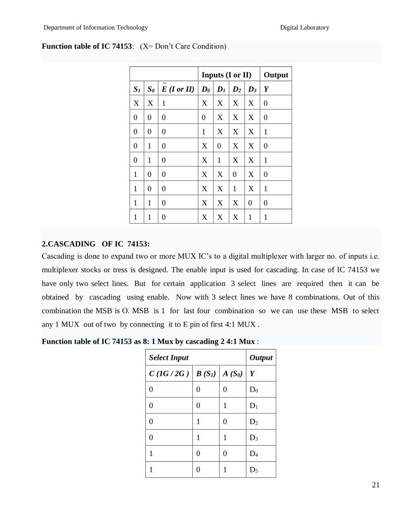
Department of Information Technology Digital Laboratory
22
1 1 0 D6
1 1 1 D7
3FUNCTION IMPLEMENTATION
Y= sum m (1 3 5 6)
Thisexpression is in Standard SOP form and it is three variable function So we need to use mux with
three select inputs ie 81 Mux Already we have implemented 81 Mux using IC 74153 For Boolean
function in Standard SOP form we connect data inputs corresponding to the minterms present in the given
function to Vcc and remaining data inputs to ground
Truth table
Inputs Output
C B A Y
0 0 0 0
0 0 1 1
0 1 0 0
0 1 1 1
1 0 0 0
1 0 1 1
1 1 0 1
1 1 1 0
LOGIC DIAGRAM
Hardware Requirements
GATE Quantity
IC Quantity
Mux 1 74153 1
NOT 1 7404 1
OR 1 7432 1
Department of Information Technology Digital Laboratory
23
Part-B Decoder (IC 74138)
Theory
Discrete quantities of information are requested in digital system with binary codes A binary code of n
bits is capable of representing into 2n distinct elements of the coded information
Decoder converts coded input to coded outputs accepts one of the code
There are different types of decoders such as 38 decoder 416 line decoders etc These are in general
called as n m line decoder where m=2n and n= no of input lines and m=no of output lines Demux also
takes one input data line source and selectively distributes it to one of n output channels The only
difference between demux and decoder is that demux has Din (data ip) line whereas decoder does not
have
ADVANTAGES
1) The decoder provides best implementation whenever there are many outputs of the combinational
circuit and each op of the function (or its complement) is required to be expressed with a small no
of minterms
2) The decoder can function as demux If the Enable ip line is taken as Din (data ip)
DISADVANTAGES
Since decoder method requires an OR gate for each op function so there is new hardware used And it is
always advisable to use minimum hardware as we come across problems like propagation delay of gates
APPLICATIONS
Decoder is worthily used for decoding binary information and memory interfacing It is used for the
implementation of Boolean function
Differentiate between Mux Demux Decoder
Point Multiplexer Demultiplexer Decoder
Input Many input lines Single input line Many input line also Acts as select line
Output Single output line Many output line Many output lineActive low output
Select line 2m = n n = 2m Enable inputs used
Department of Information Technology Digital Laboratory
24
A) Verification of IC 74138
We use IC 74138 which accepts 3 binary weighted inputs (A0 A1 A2) and when enabled provides
mutually exclusive active low outputs (y0-y7) It features 3 Enable ips Two active low (G2A G2B) and
one active high (G1) Every output will be high unless G2A G2Bare low and G1 is high It has
demultiplexing capability and multiple enable ips for easy expansion
IC Diagram
Function Table of 38 decoder
Input Output
Enable Data
G2A G2B G1 A2 A1 A0 Y0 Y1 Y2 Y3 Y4 Y5 Y6 Y7
0 0 0 X X X 1 1 1 1 1 1 1 1
0 1 1 X X X 1 1 1 1 1 1 1 1
1 0 1 X X X 1 1 1 1 1 1 1 1
1 1 1 X X X 1 1 1 1 1 1 1 1
Department of Information Technology Digital Laboratory
25
0 0 1 0 0 0 0 1 1 1 1 1 1 1
0 0 1 0 0 1 1 0 1 1 1 1 1 1
0 0 1 0 1 0 1 1 0 1 1 1 1 1
0 0 1 0 1 1 1 1 1 0 1 1 1 1
0 0 1 1 0 0 1 1 1 1 0 1 1 1
0 0 1 1 0 1 1 1 1 1 1 0 1 1
0 0 1 1 1 0 1 1 1 1 1 1 0 1
0 0 1 1 1 1 1 1 1 1 1 1 1 0
B) Cascading of IC 74138
The enable ip G1 active high of IC 74138 is used for cascadingfor cascading 2 ICrsquos the enable ip G1 of
first IC is connected to G1 enable ip of second IC through a NOT gate This enable ip is used as MSB
select ip line A3 the other three select input lines of both ICrsquos (A0A1A2) are also shorted to select
input lines of second IC to get single ip select lines (A0A1A2)
The ip line A3 is used to enable disable the 2 IC 74138 decoders When A3=0 first IC is enabled and
second is disabled Thus the first decoder will generate minterms from 0000 to 0111 as op and the second
decoder will generate nothing When A3=1 the enable conditions are reversed and thus second decoder
IC will generate minterms 1000 to 1111
Function Table of 416 decoder using IC 74138 (38 decoder)
Input Output
Enable Data
G2
A
G2
B
A
3
A
2
A
1
A
0
Y
0
Y
1
Y
2
Y
3
Y
4
Y
5
Y
6
Y
7
Y
8
Y
9
Y1
0
Y1
1
Y1
2
Y1
3
Y1
4
Y1
5
0 1 X X X X 1 1 1 1 1 1 1 1 1 1 1 1 1 1 1 1
Department of Information Technology Digital Laboratory
26
1 0 X X X X 1 1 1 1 1 1 1 1 1 1 1 1 1 1 1 1
1 1 X X X X 1 1 1 1 1 1 1 1 1 1 1 1 1 1 1 1
0 0 0 0 0 0 0 1 1 1 1 1 1 1 1 1 1 1 1 1 1 1
0 0 0 0 0 1 1 0 1 1 1 1 1 1 1 1 1 1 1 1 1 1
0 0 0 0 1 0 1 1 0 1 1 1 1 1 1 1 1 1 1 1 1 1
0 0 0 0 1 1 1 1 1 0 1 1 1 1 1 1 1 1 1 1 1 1
0 0 0 1 0 0 1 1 1 1 0 1 1 1 1 1 1 1 1 1 1 1
0 0 0 1 0 1 1 1 1 1 1 0 1 1 1 1 1 1 1 1 1 1
0 0 0 1 1 0 1 1 1 1 1 1 0 1 1 1 1 1 1 1 1 1
0 0 0 1 1 1 1 1 1 1 1 1 1 0 1 1 1 1 1 1 1 1
0 0 1 0 0 0 1 1 1 1 1 1 1 1 0 1 1 1 1 1 1 1
0 0 1 0 0 1 1 1 1 1 1 1 1 1 1 0 1 1 1 1 1 1
0 0 1 0 1 0 1 1 1 1 1 1 1 1 1 1 0 1 1 1 1 1
0 0 1 0 1 1 1 1 1 1 1 1 1 1 1 1 1 0 1 1 1 1
0 0 1 1 0 0 1 1 1 1 1 1 1 1 1 1 1 1 0 1 1 1
0 0 1 1 0 1 1 1 1 1 1 1 1 1 1 1 1 1 1 0 1 1
0 0 1 1 1 0 1 1 1 1 1 1 1 1 1 1 1 1 1 1 0 1
0 0 1 1 1 1 1 1 1 1 1 1 1 1 1 1 1 1 1 1 1 0
C) Implementation of Boolean function
The procedure for implementation of combinational circuit by means of a decoder and lsquoORrsquo gates requires
that the Boolean function fir the circuit be expressed in Sum of Minterms These forms can be obtained by
Department of Information Technology Digital Laboratory
27
expanding the function A decoder is then chosen which generates all the minterms of n ip variables The
ip to each OR gate are selected from the decoder outputs according to the minterms list in each function
i) F1=summ (1 3 5 7)
Truth table
Logic Diagram
ii) F2=summ (1 3 5 7111315)
Truth table
Logic Diagram
Conclusion In this way multiplexer Decoderamp its applications are studied implemented amp
tested
FAQrsquos
1What is a multiplexer
2What is a Demultiplexer
3 Enlist applications of multiplexer
Department of Information Technology Digital Laboratory
28
Regularity Content Viva-voce Timely
Submission Total
Dated Sign of
Subject
Teacher
2 4 2 2 10
Date of Performance Date of Completion
-------------------------------------------------------------------------------------------------------------------
Assignment No4
------------------------------------------------------------------------------------------------------------------
Title 3 bit updown Asynchronous and Synchronous counter using IC7476
------------------------------------------------------------------------------------------------------------------
Objective To understand design procedure of asynchronousamp Synchronous counter
------------------------------------------------------------------------------------------------------------------
Problem Statement Design (State diagram state table amp K map) and implementation of 3
bit Up and Down Asynchronous and Synchronous Counter using master slave JK flip-flop IC 7476
-----------------------------------------------------------------------------------------------------------------
Hardware Requirement
i) IC 7476 (MS-JK Flip-flop) IC 7408(Quad 2 ip AND Gate)
IC 7432 (Quad 2 ip OR Gate) and IC 7404 (Hex Inverter)
ii) Digital Trainer Kit -132
iii) Patch cords
----------------------------------------------------------------------------------------------------------------
Software Requirement Digital Work 30
------------------------------------------------------------------------------------------------------------------
Theory
Counters counters are logical device or registers capable of counting the no of states or no of clock
pulses arriving at its clock input where clock is a timing parameter arriving at regular intervals of time
so counters can be also used to measure time amp frequencies They are made up of flip flops Where the
Department of Information Technology Digital Laboratory
29
pulse are counted to be made of it goes up step by step amp the op of counter in the flip flop is decoded to
read the count to its starting step after counting n pulse incase of module counters
Types of Counters
Counter are of two types
1) Asynchronous counter
2) Synchronous counter
Asynchronous counter
A digital counter is a set of flip flop The flip flop are connected such that their combined state at any time
is binary equivalent of total no of pulses that have occurred up to that time Thus its name implies a
counter is used to count pulse A counter is used as frequency dividers To obtain waveform with
frequency that is specific fraction of clock frequency
Counter may be Asynchronous or synchronous The Asynchronous counter is also called as ripple counter
An Asynchronous counter uses T flip flop to perform a counting function The actual hardware used is
usually J-K flip flop with J amp K connected to logic1Even D flip flops may be used here
In asynchronous counter commonly called ripple counter the first flip-flop is clocked by the external
clock pulse amp then each successive flip-flop is clocked by the Q or Qrsquo output of the previous flip-flop
Therefore in an asynchronous counter the flip-floprsquos are not clocked simultaneously The input of MS-JK
is connected to VCC because when both inputs are one output is toggled As MS-JK is negative edge
triggered at each high to low transition the next flip-flop is triggered
Synchronous Counter
When counter is clocked such that each flip flop in the counter is
triggered at the same time the counter is called as synchronous counter
The gates propagation delay at reset time will not be present or we may say will not occur
1) Asynchronous Up Counter
Fig 1 shows 3bit Asynchronous Up Counter Here Flip-flop 2 act as a MSB Flip-flop and Flip-flop 0 act
as a LSB Flip-flop Clock pulse is connected to the Clock of Flip-flop 0 Output of Flip-flop 0(Q0) is
connected to clock of next flip-flop (ie Flip-flop 1) and so on As soon as clock pulse changes output is
going to change (at the negative edge of clock pulse) as a Up count sequence For 3 bit Up counter state
table is as shown below
Department of Information Technology Digital Laboratory
30
State Table
Logic diagram
Fig 1 3 Bit Asynchronous Up Counter
Hardware requirements
Gate
Flip flop
Quantity IC Quantity
MS JK 3 7476 2
2) Down Counter
Fig 2 shows 2 bit Asynchronous Down Counter Here Flip-flop 2 act as a MSB Flip-flop and Flip-flop 0
act as a LSB Flip-flop Clock pulse is connected to the Clock of Flip-flop 0 Output of Flip-flop 0 (Q0rsquo) is
Counter States Count
Q2 Q1 Q0
0 0 0 0
1 0 0 1
2 0 1 0
3 0 1 1
4 1 0 0
5 1 0 1
6 1 1 0
7 1 1 1
8 0 0 0
Department of Information Technology Digital Laboratory
31
connected to clock of next flip-flop (ie Flip-flop 1) and so on As soon as clock pulse changes output is
going to change (at the negative edge of clock pulse) as a down count sequence For 3 bit down counter
sate table is as shown below
In both the counters Inputs J and K are connected to Vcc hence J-K Flip flop work in toggle mode Preset
and Clear both are connected to logic 1
State Table
Logic diagram
Fig 2 3 Bit Asynchronous Down Counter
Hardware requirements
Counter States Count
Q2 Q1 Q0
7 1 1 1
6 1 1 0
5 1 0 1
4 1 0 0
3 0 1 1
2 0 1 0
1 0 0 1
0 0 0 0
7 1 1 1
Department of Information Technology Digital Laboratory
32
Gate
Flip flop
Quantity IC Quantity
MS JK 3 7476 2
Applications
The asynchronous counters are specially used as the counting devices
They are also used to count number of pulses applied
It also works as frequency divider
It helps in counting the number of product coming out of the machinery where product is coming out at
equal interval of time
Types of synchronous counter
1) Up counter
2) Down counter
1 3 bit Synchronous up counter
The up counter counts from 0 to7 ie(000 to 111)for this we are using MS JK flip flop In IC 74LS76 2
MS J-K flip flops are present The clock pulse is given at pin 1 amp 6 of the 1st IC amp pin 1 of 2nd IC Next
state decoder logic is designed with the help of state table
State table for synchronous up counter
Present state Next state Flip flop 3 Flip flop 2 flip flop 1
Q2 Q1 Q0 Q2 Q2 Q0 J2 K2 J1 K1 J0 K0
0 0 0 0 0 1 0 x 0 X 1 x
0 0 1 0 1 0 0 x 1 X x 1
0 1 0 0 1 1 0 x x 0 1 x
0 1 1 1 0 0 1 x x 1 x 1
1 0 0 1 0 1 x 0 0 X 1 X
1 0 1 1 1 0 x 0 1 X x 1
1 1 0 1 1 1 x 0 x 0 1 X
1 1 1 0 0 0 x 1 x 1 x 1
Department of Information Technology Digital Laboratory
33
K-Map
Q1Q0
Q2
00 01 11 10
0 0 0 1 0
1 X X X X
J2= Q1Q0
Q1Q0
Q2
00 01 11 10
0 X X X X
1 0 0 1 0
K2= Q1Q0
Q1Q0
Q2
00 01 11 10
0 0 1 X X
1 0 1 X X
J1= Q0
Q1Q0
Q2
00 01 11 10
0 X X 1 0
1 X X 1 0
K1= Q0
Department of Information Technology Digital Laboratory
34
Q1Q0
Q2
00 01 11 10
0 1 X X 1
1 1 X X 1
J0= 1
Q1Q0
Q2
00 01 11 10
0 X 1 1 X
1 X 1 1 X
K0= 1
Logic Diagram
Fig 1 3 bit Synchronous up counter
Department of Information Technology Digital Laboratory
35
2 3 bit Synchronous down counter
This is used to count from 7-0 ie(111-000)for this also 2 ICrsquos of 74LS76 are required amp hence we use 3
MS JK flip flops Here also clock is given to 1stamp 6th pin of 1st IC amp1st pin of 2nd IC enabling to apply
clock to all flip flop at a time Next state decoder logic is designed with the help of state table
State table for synchronous down counter
Present state Next state Flip flop 3 Flip flop 2 Flip flop 1
Q2 Q1 Q0 Q2 Q1 Q0 J2 K2 J1 K1 J0 K0
1 1 1 1 1 0 X 0 X 0 X 1
1 1 0 1 0 1 X 0 X 1 1 X
1 0 1 1 0 0 X 0 0 X X 1
1 0 0 0 1 1 X 1 1 X 1 X
0 1 1 0 1 0 0 X X 0 X 1
0 1 0 0 0 1 0 X X 1 1 X
0 0 1 0 0 0 0 X 0 X X 1
0 0 0 1 1 1 1 X 1 X 1 X
K-Map
Q1Q0
Q2
00 01 11 10
0 1 0 0 0
1 X X X X
J2= Q1Q0
Q1Q0
Q2
00 01 11 10
Department of Information Technology Digital Laboratory
36
0 X X X X
1 1 0 0 0
K2= Q1Q0
Q1Q0
Q2
00 01 11 10
0 1 0 X X
1 1 0 X X
J1= Q0
Q1Q0
Q2
00 01 11 10
0 X X 0 1
1 X X 0 1
K1= Q0
Q1Q0
Q2
00 01 11 10
0 1 X X 1
1 1 X X 1
J0= 1
Q1Q0
Q2
00 01 11 10
0 X 1 1 X
1 X 1 1 X
K0= 1
Department of Information Technology Digital Laboratory
37
Logic Diagram
Fig 2 3 bit Synchronous down counter
Uses
1 Specially used as the counting devices
2 Used in frequency divider circuit
3 Used in digital voltmeter
4 Used in counter type A to D converter
5 Used for time measurement
6 It helps in counting the no of product coming out from machinery where product is coming out
at equal interval of time
Conclusion
Up and down counters are successfully implemented the counters are studied amp op are checked The
state table is verified
PRACTICE ASSIGNMENTS EXERCISE MODIFICATIONS
1 Design amp implement 2 bit controlled synchronous counter
2 Designamp implement 4 bit controlled synchronous counter
3 Designamp implement truncated synchronous up or down counter
FAQrsquos with answers
1 What do you mean by Counter
A Counter is a register capable of counting the no of clock pulses arriving at its
clock inputs Count represents the no of clock pulses arrived A specified
sequence of states appears as the counter output
Department of Information Technology Digital Laboratory
38
2 What are the types of Counters Explain each
There are two types of counters as Asynchronous Counter and Synchronous Counter
Asynchronous Counter In this counter the first flip-flop is clocked by the external clock pulse
and then each successive flip-flop is clocked by the Q or Qrsquo op of the previous flip-flop Hence in
Asynchronous Counter flip-flops are not clocked simultaneously and hence called as Ripple
Counter Synchronous Counter In this counter the common clock input is connected to all the
flip-flops simultaneously
3 What do you mean by pre-settable counters
A counter in which starting state is not zero can be designed by making use of the
preset inputs of the flip flops This is referred to as loading the counter
asynchronously This is referred to as pre-settable counter
4 What are the applications of synchronous counters
Digital clock
Frequency divider circuits
Frequency counters
Used in analog to digital converters
5 What are the advantages of synchronous counters over asynchronous counters
Propagation delay time is reduced
Can operate at a much higher frequency than the asynchronous counters
6 Ring counter is an example of synchronous counters or asynchronous counter
Synchronous counter Since all the flip flops are clocked simultaneously
7 Twisted Ring (Johnsonrsquos) counter is an example of synchronous counters or asynchronous
counter
Synchronous counter Since all the flip flops are clocked simultaneously
8 What is the difference between ring counter and twisted ring counter
In ring counter pulses to be counted are applied to a counter it goes from state to state and the
output of the flip flop s in the counter is decoded to read the count Here the uncomplimentary
output (Q) of last flip flop is fed back as an input to first flip flop Ring counters are referred as
MOD lsquoNrsquo counters
Department of Information Technology Digital Laboratory
39
But in Twisted ring counter the complimentary output (Q bar) of last flip flop is fed back as an
input to first flip flop Twisted Ring counters are referred as MOD lsquo2Nrsquo counters
9 What are the applications of ring counters
Ring counter outputs are sequential non-overlapping pulses which are useful for control state
counters Used in stepper motor this requires pulses to rotate it from one position to the next Used
as divide by lsquoNrsquo ((MOD lsquoNrsquo) counters
10 What are the applications of ring counter twisted ring counters
Used as divide by lsquo2Nrsquo ((MOD lsquo2Nrsquo) counters
Used for control state counters
Used for generation of multiphase clock
11 List the Synchronous Counter ICs
IC 74160 Decade Up Counter
IC 74161 4 bit binary Up Counter
IC 74162 Decade Up Counter
IC 74163 4 bit binary Up Counter
IC 74168 Decade UpDown Counter
IC 74169 4 bit Binary UpDown Counter
IC 74190 Decade UpDown Counter
IC 74191 4 bit Binary UpDown Counter
IC 74192 Decade UpDown Counter
IC 74193 4 bit Binary UpDown Counter
Department of Information Technology Digital Laboratory
40
Regularity Content Viva-voce Timely
Submission Total
Dated Sign of
Subject
Teacher
2 4 2 2 10
Date of Performance Date of Completion
-------------------------------------------------------------------------------------------------------------------
Assignment No 5
-------------------------------------------------------------------------------------------------------------------------------
Title Design and implementation of Module lsquonrsquo counter with IC7490 and IC 74191
-----------------------------------------------------------------------------------------------------------------------------
Objective To know difference between regular amp truncated counter as well as binary ampBCD Counter
--------------------------------------------------------------------------------------------------------------------------------
Problem Statement To design and implement mod - 10 mod ndash 7 mod - 99 asynchronous BCD
counter using IC 7490 and to design and implement up down mod - n Binary counter using IC 74191
-----------------------------------------------------------------------------------------------------------------
Hardware Requirement
i) IC 7490 IC 74191 basic gates
ii) Digital Trainer Kit -1
iii) Patch cords
----------------------------------------------------------------------------------------------------------------
Software Requirement Digital Work 30
------------------------------------------------------------------------------------------------------------------
Theory
Part A ndash IC 7490
IC 7490 is a TTL MSI (medium scale integration) decade counter It contains 4 master slave flip flops
internally connected to provide MOD-2 ie divide by 2 and MOD-5 ie divide by 5 counters MOD-2 and
Mod-5 counters can be used independently or in cascading
Department of Information Technology Digital Laboratory
41
It is a 4-bit ripple type decade counter The device consists of 4-master slave flip flops internally
connected to provide a divide by two and divide by 5 sections Each section has a separate clock ip to
initiate state changes of the counter on the high to low clock transition
Since the op from the divide by 2 section is not internally connected to the succeeding stages The device
may be operated in various counting modes In a BCD counter the CP1 input must be externally connected
to QA op The CP0ip receives the incoming count producing a BCD count sequence It is also provided
with additional gating to provide a divide by 2 counter and binary counter for which the count cycle length
is divide by 5 The device may be operated in various counting modes
There are 2 reset inputs R0(1) and R0(2) both of which need to be connected to the lsquologic 1rsquo for clearing all
flip flops Two set inputs Rg(1) and Rg(2) when connected to logic 1 are used for setting counter to 1001
(BCD 9)
Pin out of IC 7490
Fig Pin configuration of IC7490
Table 1-pin name and description of IC7490
Pin name Description
Input B This is clock input to the internal MOD-5 ripple counter which is negative
edge triggered
R0(1)R0(2) Gated zero reset inputs
Department of Information Technology Digital Laboratory
42
R9(1)R9(2) These are gated set to nine inputs
QDQCQB Output of internal MOD-5 counter with QD as MSB
QA Output of internal MOD-2 counter with QA as LSB
Input A Clock input to FF-A which is negative edge triggered
Functional Table for IC7490
Reset inputs Output
R0(1) R0(2) R9(0) R9(1) QD QC QB QA
1 1 0 X 0 0 0 0
1 1 X 0 0 0 0 0
X X 1 1 1 0 0 1
X 0 X 0 COUNTER
0 X 0 X COUNTER
0 X X 0 COUNTER
X 0 0 x COUNTER
Department of Information Technology Digital Laboratory
43
Basic internal Structure of IC 7490
Function Table of MOD-5 counter
Design of MOD-10 counter using IC 7490
The QA op the first flip flop is connected to the input B which is clock ip of internal MOD-5 ripple
counter Due to cascading of Mod-2 and Mod-5 counters the overall configuration the decade counters
count from 0000 to 1001 After 1001 mod-5 resets to 0000 and next count after 1001 is 0000
When QA op is connected to B ip we have the Mod-2 counter followed by Mod-5 counter The
count sequence obtained is shown in the table It may be noted that QA changes from 0 to 1 the state of
InputB clock Output
Count QD QC QB
0 0 0 0
0 0 1 1
0 1 0 2
0 1 1 3
1 0 0 4
Department of Information Technology Digital Laboratory
44
Mod-5 counter doesnrsquot change whereas when QA changes from 1 to 0 the Mod-5 counter goes to the next
state
Logic DiagramMOD-10 counter using IC 7490
5 Modulus n Counter
Function table
Ip clock
Output
Count QD QC QB QA
0 0 0 0 0
0 0 0 1 1
0 0 1 0 2
0 0 1 1 3
0 1 0 0 4
Department of Information Technology Digital Laboratory
45
Design of Mod-7 Counter using IC 7490
Mod-7 counter counts through seven states from 0 to 6 counters and it should reset as soon as the
count becomes 7 The op of reset logic should be 1 corresponding to invalid states The reset logic op
should be applied to pin 2 and 3
Truth Table of Reset Logic
0 1 0 1 5
0 1 1 0 6
0 1 1 1 7
1 0 0 0 8
1 0 0 1 9
QD QC QB QA Y
0 0 0 0 0
0 0 0 1 0
0 0 1 0 0
0 0 1 1 0
0 1 0 0 0
0 1 0 1 0
0 1 1 0 0
0 1 1 1 1
1 0 0 0 1
1 0 0 1 1
Department of Information Technology Digital Laboratory
46
Logic Diagram Mod 7 Counter using IC 7490
Function table
Ip clock
Output
Count QD QC QB QA
0 0 0 0 0
0 0 0 1 1
0 0 1 0 2
0 0 1 1 3
0 1 0 0 4
0 1 0 1 5
0 1 1 0 6
Department of Information Technology Digital Laboratory
47
Design of Mod-99 using IC 7490
For Mod-99 two IC 7490rsquos will be required Hence to implement a divide by 99 counter we have
to use two decade counters ICrsquos A divide by 99 counter counts 99 states from 0 to 98 and the counter
should reset as soon as the count becomes 99 So in order to reset the counter of 99 connect the Q op
which are equal to 1 in the count of 99 to an lsquoAndrsquo gate amp then connect and op to the reset ip of both
ICrsquos
MOD-100 Counter-
MOD-100 counter can be obtained by cascading two decade counter ICrsquos
Each IC gives divide by 10 counts Hence 2 ICs will give 1010=100 counts
Clock is applied to the input A of IC 7490 the Q1 output is connected to B input etc
For cascading the QD output of the first IC is connected to the input A of second IC Thus QD of
IC-(1) acts as clock input to IC-(2)
The Ro (1) Ro(2) R9(1) R9(2) inputs of both ICs are connected to ground so as to make them
inactive
The total count provided by the two counters varies from 00 to 99 decimal that means 100 states
Hence it is a MOD-10 counter
Impleacutementations
FigureMOD-100 counters using IC 7490
Department of Information Technology Digital Laboratory
48
B) IC 74191 ndash Theory
IC74191 is 4-bit binary synchronous reversible up down counter It contains 4 master slave flip flops
with internal gating and steering logic to provide asynchronous reset and synchronous count updown
operations its asynchronous parallel capability permits the counter to be preset to any desire number D0
to D3 are the parallel data inputs Information present on the parallel data inputs D0 to D3 is loaded into
the counter and appears on the output when the load PLinput is lowThisoperation overrides the counting
function Counting is inhabited by the high level on the enable G input when G input is low internal state
changes are initiated synchronously by the low to high transitions of the clock inputs the updown input
signal determines the direction of input
Function Table
Operating
mode
Inputs Outputs
PL UD G CLK Dn
Parallel
load L X X X L L
L X X X H H
Count up H L 0 uarr X Count up
Count
down H H 0 uarr X
Count
down
Hold(No
change) H X H X X No change
Pin details ndash
D0 to D3 input lines PL parallel load
G is Enable input ndash enabling the counting
Q0 to Q3 output lines
Downup determines the direction of counting
Clk clock input for counter
Terminal Count Max(1111) min(0000) For these states signal goes high for 1clock pulse
Ripple clock Clock input for next higher state
Department of Information Technology Digital Laboratory
49
Pin Diagram IC 74191
Up counter- Truth Table
Clk
Pulses QA QB QC QD
0 0 0 0 0
1 0 0 0 1
2 0 0 1 0
3 0 0 1 1
4 0 1 0 0
5 0 1 0 1
6 0 1 1 0
7 1 1 1 1
8 1 0 0 0
9 1 0 0 1
10 1 0 1 0
11 1 0 1 1
12 1 1 0 0
13 1 1 0 1
Department of Information Technology Digital Laboratory
50
14 1 1 1 0
15 1 1 1 1
Logic Diagram
Steps-
Connect the circuit as shown above
Apply clock ip to pin no14
Connect UD to GND
Verify the output according to truth table
Logic diagram of down counter
Steps-
Connect the circuit as shown above
Apply clock ip to pin no14
Connect UD to VCC
Verify the output according to truth table
UD D3 D2 D1 D0 PL
Clock IC 74191
G RC
MAX MIN
Q3 Q2 Q1 Q0 TC
vcc
NC
NC
Outputs
no connection
vcc
Department of Information Technology Digital Laboratory
51
With the help of IC74191 we can implement truncated updown counter by using following logic ndash
Connect data input line to particular count you want to load
According to requirement make Truth table
Draw the K-map
Find out Boolean expression
Draw the logic diagram and that is the combinational logic for your count and apply the output of
that circuit to PL
According to requirement we get the UP and down counting
5 Modulus n Counter
Presettable updown counter
Mod 11 counter
Implementation of presetttable mod updown counter using IC- 74LS191
1 Load Data on data lines D0 to D3 (0101)
2 Counter will go through the states from 0101 0110hellip1111 in up counter and 0101 to 0000 in
down counter
Combinational Circuit
CLOCK D3 D2 D1 D0
TC
U D 74191 RC
G PL
Updown Q3 Q2 Q1 Q0 PL
Q3 Q2 Q1 Q0
Preset Count
Department of Information Technology Digital Laboratory
52
3 The logic circuit should be designed in such a way that only when all the outputs are high output
of the reset circuit should be low and the counter should jump to state 5 It should again start
counting from 0101 to 0000
State Table
Down Counter UP Counter
IC 74191 is 4 bit counter Thus it counts 0000 to 1111 different 16 states For MOD11 counter we require
different 11 states so 5 steps must be skipped from 16 states We get MOD11 by presetting counter to
value 5
Assignment Question
Design and Implement MOD 7 MOD 10 and MOD 12 using IC 74191
FAQs
1 What do you mean modulus counter
Counter
state Clock
pulse
Q3 Q2 Q1 Q0
1 0 1 0 1
2 0 1 1 0
3 0 1 1 1
4 1 0 0 0
5 1 0 0 1
6 1 0 1 0
7 1 0 1 1
8 1 1 0 0
9 1 1 0 1
10 1 1 1 1
11 1 1 1 1
Counter state
Clock pulse
FF outputs
Q3 Q2 Q1 Q0
1 0 1 0 1
2 0 1 0 0
3 0 0 1 1
4 0 0 1 0
5 0 0 0 1
6 0 0 0 0
7 0 1 0 1
Department of Information Technology Digital Laboratory
53
It represents the number of possible states of counter
2 How will you use the 7490 IC to design symmetrical divide by 10 frequency counter
The divide by 5 circuit followed by divide by 2 circuit will give symmetrical output
3Where counters are used Give real life example of counter
Modulus n Counter
Binary counter ndash An N stage counter that recycles after 2 Ncount The count proceds in specified binary
sequence Counter Presetable- A counter which can be set to a desired value before the start of the
counting UPDown counter ndash A counter that can count in both up and down direction depending upon a
control input
Department of Information Technology Digital Laboratory
54
Regularity Content Viva-voce Timely
Submission Total
Dated Sign of
Subject
Teacher
2 4 2 2 10
Date of Performance Date of Completion
-------------------------------------------------------------------------------------------------------------------
Assignment No6
------------------------------------------------------------------------------------------------------------------
Title Sequence Generator
------------------------------------------------------------------------------------------------------------------
Objective To understand sequence generator one of the sequential circuit
-------------------------------------------------------------------------------------------------------------------
Problem Statement Design (State Diagram State Table K Map) and implementation of Sequence
Generator using Shift Register IC 74194
-----------------------------------------------------------------------------------------------------------------
Hardware Requirement
i) IC 741947408 (AND-gate) 7432 (OR-gate)
ii) Digital Trainer Kit -1
iii) Patch cords
----------------------------------------------------------------------------------------------------------------
Software Requirement Digital Work 30
------------------------------------------------------------------------------------------------------------------
Theory
Part A Sequence Generator with Flip flop
A sequential circuit which generates a prescribed sequence of bits in synchronism with a clock is referred
to as a sequence generator These pulse trains or sequence of bits can be used to open valves close gates
turn on lights and turn off machines and other variety of jobs
Department of Information Technology Digital Laboratory
55
For the design of sequence generator we first determine the required no of flip flops and the logic circuit
for the next state decoder
No of flip flops required to generate particular sequence can be determined as follows
1) Find the no of 1rsquos in the sequence
2) Find the no of 0rsquos in the sequence
3) Take the maximum out of two
4) If N is the required no of flip flops choose minimum value of lsquonrsquo to satisfy equation given below
Max (0rsquos 1rsquos) le 2n-1
The sequence generator can be classified as
1) sequence generator without bushing
2) sequence generator with bushing
The aim in this experiment is to design a sequence generator to generate a sequence of bit ie 10101
Part B Sequence Generator using Shift Register IC 74194
IC 74194 4 bit bidirectional Shift Register
This bidirectional shift register is designed to incorporate virtually all the features a system designer may
want in a shift register they feature Parallel inputs parallel outputs right shift left shift serialinputs
operating mode control inputsand a direct overriding clear line The register has four distinct modes of
operationsnamely
1 Parallel load
2 Shift right (in the direction QA towards QD)
3 Shift left (in the direction QD towards QA)
4 Inhibit clock (do nothing)
Synchronous parallel loading is accomplished by applying the four bits of data and taking both
mode control inputs S0 and S1High The data is loaded in to the associated flip-flops and appear
at the outputs after positive transition of the clock input During loading serial data flow is
inhibited
Shift right is accomplished synchronously with the rising edge of the clock pulse when S0 is High
and S1 is Low Serial data for this mode is entered at the shift right data input When S0 is Low
and S1 is High data shifts left synchronously and new data is entered at the shift left serial input
Clocking of the flip flop is inhibited when both mode control inputs are LOW
Department of Information Technology Digital Laboratory
56
Mode Control Input Operation
S1 S0
0 0 Clock Inhibit
0 1 Shift right
1 0 Shift Left
1 1 Parallel loading
Function Table of IC 74194
Design
The minimum number of flip-flops N required to generate a sequence of length S is given by S
le 2N ndash 1
In this case S=7 therefore the minimum value of N which may generate in this sequence is 3
However it is not guaranteed to lead to a solution If the given sequence leads to seven distinct
states then only three flip flops are sufficient otherwise we have to increase the number of flip
flops We write the states of circuit as given in table 1 The prescribed sequence is listed under QA
and the sequence listed under QB and QC are the same sequence delayed by one and two clock
pulses respectively From the table we observe that all the states are not distinct which means N=3
is not sufficient Next we assume that N=4 and prepare table 2 The last column gives the required
serial input for getting the desired change of state when a clock pulse is applied This is obtained
by assuming D type flip flop and looking at the QA output For example at the falling edge of first
clock pulse QA=1 The second clock pulse must result in QA=1 which requires its D input to be 1
In the same manner all the entries in column Y are determined
Table 1 State Assignment Table of Sequence Generator (N=3)
Number of Clock
Pulses
Flip Flop Inputs States
QA QB QC
1 1 1 1 7
2 1 1 1 7
3 0 1 1 3
4 1 0 1 5
Department of Information Technology Digital Laboratory
57
5 0 1 0 2
6 1 0 1 5
7 1 1 0 6
Excitation table of D Flip-Flop
Present State Qn Next State Qn+1 Flip-Flop Input D
0 0 0
0 1 1
1 0 0
1 1 1
Table 2State Assignment Table of Sequence Generator (N=4)
Number of Clock
Pulses
Flip Flop Inputs States
Y
Serial ip QA QB QC QD
1 1 1 1 0 14 1
2 1 1 1 1 15 0
3 0 1 1 1 7 1
4 1 0 1 1 11 0
5 0 1 0 1 5 1
6 1 0 1 0 10 1
7 1 1 0 1 13 1
K-Map Simplification
Department of Information Technology Digital Laboratory
58
00 01 11 10
00 X X X X
01 X 1 1 X
11 X 1 0 1
10 X X 0 1
Y= QArsquo + QBrsquo + QCrsquo = QAQBQC
LOGIC DIAGRAM
HARDWARE REQUIREMENTS
Sr no ICs Description Quantity
11 74194 4 bit bidirectional universal shift register 16ktr`
2 7410 3 input NAND Gate 1
Department of Information Technology Digital Laboratory
59
Conclusion In this way sequence generator using JK flip flips amp shift register is designed and
implemented
Enhancements Modifications ndash Sequence generator can also be implemented with shift register instead
of flip flops Use IC 7495 universal shift register IC and try to implement sequence generator
FAQs
1 What is sequential logic circuit
A sequential logic circuit consists of a memory elements in addition to
combinational circuit Its output at any instant of time depends upon
the present input as well as present state of memory element
2 What is meant by delay line
It is used to introduce time delays in digital signals
3 What is meant by following terms
a) Synchronous preset b) Asynchronous preset
c) Synchronous clear d) Asynchronous clear
a)Preset operation is synchronised with the clock
b)Preset operation is independent of the clock
c) clear is performed in synchronous with clock
d) clear is performed independent with clock
4 Is asynchronous counter faster than synchronous counter
In a synchronous counter the time required for change of any state is same and is equal to delay
time of one flip flop where as in asynchronous counter all flip flops are not clocked
simultaneously hence time required is not same
5 What is mean by lockout in counter
In a counter design for a fewer state than the maximum possible state some time it may so happen
that counter enters in unused state and goes from one unused state to another unused state and
never comes to used state
6 What is mean by state table
Department of Information Technology Digital Laboratory
60
It consists of complete information about present state and next state and outputs of a sequential
system
7 What is mean by state diagram
The information available in a state table can be represented as graphically the graphical
representation is known as state diagram
8 What is the advantage of state reduction in the design of sequential circuit
It reduces the number of flip flops
9 What is meant by excitation table
This gives information about what should be the flip flop inputs if outputs are specified before and
after the clock pulse
10 How many flip flops are required to design sequence generator using Counters
max (0rsquoS1rsquoS) in a given sequence lt= 2(N - 1)
Where N = Number of flip flops
11 How many flip flops are required to design sequence generator using shift registers
Slt= 2N - 1
Where N=Number of flip flops
S= Length of sequence
12 What is Lock out condition How it is avoided
When counter enters into one of the invalid state and after application of pulses remains in invalid
states only i e counter gets locked into invalid state amp this is called as lock out Lock out can be
avoided by providing bushing to all the invalid states in such a way that after application of one or
more clock pulses counter will fall into one of the valid state
Department of Information Technology Digital Laboratory
61
Regularity Content Viva-voce Timely
Submission Total
Dated Sign of
Subject
Teacher
2 4 2 2 10
Date of Performance Date of Completion
-------------------------------------------------------------------------------------------------------------------
Assignment No7
------------------------------------------------------------------------------------------------------------------
Title Multiplexer using Data flow modeling and structural modeling
------------------------------------------------------------------------------------------------------------------
Objective To learn data flow modeling style Its uses and different types of declarations with some
different types of circuits Structure of VHDL program is well discussed with this modeling style
-------------------------------------------------------------------------------------------------------------------
Problem Statement 41 multiplexer using data flow amp structural modeling -
----------------------------------------------------------------------------------------------------------------
Hardware Requirement - NA
----------------------------------------------------------------------------------------------------------------
Software Requirement Xilinx
------------------------------------------------------------------------------------------------------------------
Theory
Data flow style-
In this type of design the view of data as flowing from input to output through a design
An operation is defined in terms of a collection of data transformation expressed as concurrent
statement Each of the statement can be activated when any of its input signal changes its value While
these statements describe the behavior of the circuit a lot of information about its structure can be
extracted from the description as well
Data flow modeling has a set of concurrent assignment statements In the data flow level of abstraction we
describe how information is passed in the circuit The built in operators in VHDL are used in expression
such as AND OR XOR NOT etc
Department of Information Technology Digital Laboratory
62
INPUT
Two select lines S1S0
Four data lines D0 D1 D2 D3
OUTPUT
One output line Y
Functional block diagram of 41 Mux
Fig 41 Multiplexer using Data flow modeling
Function table of 41 Mux
Enable S1 S0 A B C D Y
1 X X X X X X 0
0 0 0 A X X X A
0 0 1 X B X X B
0 1 0 X X C X C
0 1 1 X X X D D
Design steps
Click on Xilinx ISE 92i
Create New project from file menu Ensure top level source is HDL
Select family of devices (usually spartan2E or 3)
Department of Information Technology Digital Laboratory
63
Ensure preferred language is VHDL
Click new source which shows you project details device details
and Synthesis and simulator tools
After finishing project create new source by right clicking in project name with VHDL
module
Complete ports name directions and bus Ensure architecture name is behavioral
After that we will get design summary and detailed reports
Close design summary
Create your code with given modeling style
Go to process window and synthesis to check if any error is there in code Check syntax and
view RTL schematic
Create new source to simulate the code
Right click on source name and create test bench waveform with proper name Ensure the
project is same
Click on combinational circuit in initial timing wizard
Select test bench wave in source window Apply inputs to wave diagram Ensure you are in
behavioral simulation
Go to process box Click on Xilinx ISE simulator and simulate the model See results
RTL Schematic
Department of Information Technology Digital Laboratory
64
Timing Diagram
FAQrsquos
1 What are the different kinds of data objects in VHDL code
Ans data object may be any value or number still some signal data objects and bit and bit_vector
types of these are available in VHDL STD_LOGIC and STD_LOGIC_VECTOR types are used
widely in programming
2 What do you mean by signal
Ans signal is a data object represents logic signals or wires in a circuit There are three places in
which signals can be declared in VHDL code in an entity declaration in the declarative section of
architecture and in declarative section of package
3 What are different signal types
Ans BIT BIT_VECTOR STD_LOGIC STD_LOGIC_VECTOR STD_ULOGIC SIGNED
UNSIGNED INTEGER ENUMERATION and BOOLEAN
4 What is an entity
Ans a circuit or sub circuit described with VHDL code is called a design entity
5 Explain structure of an entity
Ans it has two main parts the entity declaration which specifies the input and output signals for
entity and the architecture which gives circuit details
Department of Information Technology Digital Laboratory
65
6 How will you declare a package with component Explain structure
The general form of package declaration is as shown in diagram
PACKAGE package_name IS
[TYPE declarations]
[SIGNAL declarations]
[COMPONENT declarations]
END package_name
Entity
Declaration Architecture
Department of Information Technology Digital Laboratory
66
Regularity Content Viva-voce Timely
Submission Total
Dated Sign of
Subject
Teacher
2 4 2 2 10
Date of Performance Date of Completion
-------------------------------------------------------------------------------------------------------------------
Assignment No8
------------------------------------------------------------------------------------------------------------------
Title Full Adder using Behavioral and Structural modeling
------------------------------------------------------------------------------------------------------------------
Objective To learn structural modeling style Its uses and different types of declarations with some
different types of circuits Structure of VHDL program is well discussed with this modeling style
-------------------------------------------------------------------------------------------------------------------
Problem Statement Full adder using behavioral amp structural modeling
-----------------------------------------------------------------------------------------------------------------
Hardware Requirement - NA
----------------------------------------------------------------------------------------------------------------
Software Requirement Xilinx
------------------------------------------------------------------------------------------------------------------
Theory
Structural style-
A digital electronic system can be described as a module with inputs andor outputs The electrical values
on the outputs are same functions of the values of inputs The example of it is as shown The NAND gate
has 2ips AampB amp an output y Using VHDL terminology we call the NAND2 design entity amp the inputs
amp outputs are called ports 1 way of describing the function of NAND2 is to describe how it is composed
of sub modules AND amp INVERTER Each of the Sub modules is an instance of some entity amp ports of the
instances are connected using signals Structural modeling has a set of interconnected component
Structure can be used to create a very low level description of a circuit or a very high level description
Department of Information Technology Digital Laboratory
67
In a gate level description of a circuit for example components such as basic logic gates amp FFs might be
connected in some logical stricture to create the circuit This is what is often called a net list
Structure of structural modeling
Functional block diagram of Full Adder
architectureNetlistofHalf_Adderis
-- component with locals
componentMyXorport (A_XorB_Xor in BIT
Z_Xor out BIT)
end component
-- component with locals
componentMyAndport (A_AndB_And in BIT
Z_And out BIT)
end component
begin
Xor1 MyXorport map (X Y Sum)
-- instance with actuals
And1 MyAndport map (X Y Cout)
-- instance with actuals
end
Department of Information Technology Digital Laboratory
68
Function table of Full Adder
A B Cin SUM CARRY
0 0 0 0 0
0 0 1 1 0
0 1 0 1 0
0 1 1 0 1
1 0 0 1 0
1 0 1 0 1
1 1 0 0 1
1 1 1 1 1
Sum = Σm(1 2 4 7)
Carry= Σm(3 5 6 7)
Design steps
Click on Xilinx ISE 92i
Create New project from file menu Ensure top level source is HDL
Select family of devices (usually spartan2E or 3)
Ensure preferred language is VHDL
Click new source which shows you project details device details
and Synthesis and simulator tools
After finishing project create new source(full adder) by right clicking in project name with
VHDL module
Complete ports name directions and bus Ensure architecture name is behavioral
After that we will get design summary and detailed reports
Close design summary
Click new source which shows you project details device details
and Synthesis and simulator tools
After finishing project create new source(half adder) by right clicking in project name with
VHDL module
Complete ports name directions and bus Ensure architecture name is behavioral Names
should be same as previous inputs
Department of Information Technology Digital Laboratory
69
After that we will get design summary and detailed reports
Close design summary
Create your code for half adder with given modeling style
After that go to process window Click on design utilities
View HDL instantiation code of half adder
Copy component part of half adder in architecture block of full adder Copy instantiation
template twice after begin as we require two half adders to construct full adder (structural
modeling) Name them differently (eg ha1 or ha2)
Create signals as per the logic Complete code of full adder
Go to process window and synthesis to check if any error is there in code Check syntax and
view RTL schematic
Create new source to simulate the code
Right click on source name and create test bench waveform with proper name Ensure the
project is same
Click on combinational circuit in initial timing wizard
Select test bench wave in source window Apply inputs to wave diagram Ensure you are in
behavioral simulation
Go to process box Click on Xilinx ISE simulator and simulate the model See results
RTL Schematic
Timing Diagram
Department of Information Technology Digital Laboratory
70
INPUT
Three inputs A B Carry (previous)
OUTPUT
Two outputs Sum Carry
FAQrsquos
1 What do you mean by structural style
Ans in this type of code a circuit is described in hierarchical fashion by connecting together sub
circuits
2 Explain IF statement with example
Ans The general form of an IF statement is as follws
IF Sel=rsquo0rsquo THEN
Flt=x1
ELSE
Flt=x2
END IF
Department of Information Technology Digital Laboratory
71
3 Explain declaration and instantiation process in VHDL
Ans first declare a small vhdl code in formal way Eg half adder Define project name is full adder
And simply copy instantiation template in main source code Define how many times you want to
declare this template Give separate names for those
4 What is STD_LOGIC_VECTOR
Ans It is standard data object added to VHDL standard in IEEE 1164 It provides more flexibility
than the Bit type
5 Explain difference between concurrent and sequential statements
Ans Concurrent statements define interconnected processes and blocks that together describe a designrsquos
overall behavior or structure They can be grouped using block sstatement Groups of blocks can also be
partitioned into other blocks At this same level a VHDL component can be connected to define signals
within the blocks
It is a reference to an entity A process can be a single signal assignment statement or a series of
sequential statements (SS) Within a process procedures and functions can partition the sequential
statements
PRACTICE ASSIGNMENTS
1 Implement half adder using data flow modeling
2 Implement Full Adder using behavioral modeling
3 Implement 3 bit magnitude comparator using a 3 bit adder
4 Implement half sub tractor using data flow modeling
5 Write VHDL code for Full Subtractor
Department of Information Technology Digital Laboratory
72
Regularity Content Viva-voce Timely
Submission Total
Dated Sign of
Subject
Teacher
2 4 2 2 10
rsquozaDate of Performance Date of Completion
-------------------------------------------------------------------------------------------------------------------
Assignment No9
------------------------------------------------------------------------------------------------------------------
Title Simulation of 3 bit Connter using Behavioral modeling
------------------------------------------------------------------------------------------------------------------
Objective To learn behavioral modeling style Its uses and different types of declarations with some
different types of circuits Structure of VHDL program is well discussed with this modeling style
-------------------------------------------------------------------------------------------------------------------
Problem Statement 3 bit controlled up down synchronous counter with preset amp clear
-----------------------------------------------------------------------------------------------------------------
Hardware Requirement -NA
----------------------------------------------------------------------------------------------------------------
Software Requirement Xilinx
------------------------------------------------------------------------------------------------------------------
Theory
Behavioral style-
Highest level of abstraction supported in VHDL is called the behavior level of abstraction In it we have
for loop while loop If then else case ampvariable assignment The statements are enclosed in a PROCESS
block amp are executed sequentially
In it circuit is described in terms of its operation overtime
In behavioral description the concept of time may be expressed precisely with actual delays between
related events (such as the propagation delays within gates amp on wires) or it may be simply an ordering of
operation that are expressed sequentially (such as in a functional description of a FF)
Department of Information Technology Digital Laboratory
73
A behavioral design method defines a circuit in terms of text language rather than a schematic of
interconnected symbols
Behavioral design is a technology independent text based design that incorporates high level
functionality amp high level information flow
Structure of Behavioral modeling
Functional block diagram of 3 bit controlled up down synchronous counter with preset amp clear
Function table of 3 bit controlled up down synchronous counter with preset amp clear
Design steps
Click on Xilinx ISE 92i
Create New project from file menu Ensure top level source is HDL
Select family of devices (usually spartan2E or 3)
Ensure preferred language is VHDL
Click new source which shows you project details device details
and Synthesis and simulator tools
After finishing project create new source by right clicking in project name with VHDL
module
Complete ports name directions and bus Ensure architecture name is behavioral
After that we will get design summary and detailed reports
Close design summary
Create your code with given modeling style
Go to process window and synthesis to check if any error is there in code Check syntax
and view RTL schematic Create new source to simulate the code
Department of Information Technology Digital Laboratory
74
Right click on source name and create test bench waveform with proper name Ensure the
project is same
Click on combinational circuit in initial timing wizard
Select test bench wave in source window Apply inputs to wave diagram Ensure you are in
behavioral simulation
Go to process box Click on Xilinx ISE simulator and simulate the model
RTL Schematic
Timing Diagram
INPUT
Clock Preset Clear
OUTPUT
Three output lines
FAQrsquos
1 Explain the structure of behavioral modeling
2 What are the differences between behavioral and structural modeling
Ans Behavioral descriptionof a circuit is the highest level of abstraction in VHDL Here the
circuit is described in terms of it operation with respect to time All operations are in one level of
code The operations are described in a way that the designer of a sequential circuit infers a
register
Structural description on the other hand is a circuit description in terms of its components
it can either create a low level description much like a hierarchy in a block diagram Whenever
you see a component instantiated in a code that code employs structural description of the circuit
The components are connected in the form of a netlist This is for better manageability and
reusability
3 What are the differences between behavioral and data flow modeling
Department of Information Technology Digital Laboratory
75
Ans Behavioral ndash describes how the output is derived from the inputs using structured
statements
Dataflow ndash describes how the data flows from the inputs to the output most often
using NOT AND and OR operations
4 What do you mean by process statement
Ans The process statement begins with the PROCESS keyword followed by a parenthesized list
of signals called the sensitivity list It operates on selected and conditional statements
5 Explain syntax of process statement
Ans BEGIN
Process( sensitivity list)
END process
PRACTICE ASSIGNMENTS
1 Implement 3 bit asynchronous up counter using behavioral modeling
2 Implement 3 bit asynchronous down counter using behavioral modeling
3 Implement 3 bit synchronous down counter using behavioral modeling
End
Department of Information Technology Digital Laboratory
76
Pin Diagrams
7400 Quad 2-Input NAND Gate
7402 Quad 2-Input NOR Gate
7404 Not Gates
7408 Quad 2-Input AND Gates
7432 Quad 2-Input OR Gate
7486 Quad 2-Input Exclusive-OR Gate
Department of Information Technology Digital Laboratory
77
7483 4 bit Binary Adder
7490 Decade and Binary Counters
74138 38 Decoder
Department of Information Technology Digital Laboratory
78
74153 Dual 41 Multiplexer
74191 Synchronous UpDown 4 bit Binary counter with Mode Control
Department of Information Technology Digital Laboratory
79
74194 Universal Shift Register
7476 Dual Master-Slave J-K Flip-Flops
- Part B Sequence Generator using Shift Register IC 74194
-
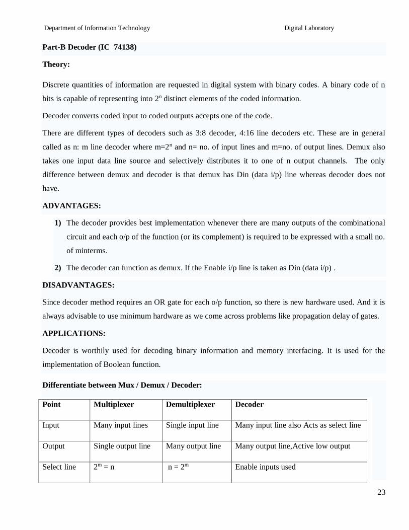
Department of Information Technology Digital Laboratory
23
Part-B Decoder (IC 74138)
Theory
Discrete quantities of information are requested in digital system with binary codes A binary code of n
bits is capable of representing into 2n distinct elements of the coded information
Decoder converts coded input to coded outputs accepts one of the code
There are different types of decoders such as 38 decoder 416 line decoders etc These are in general
called as n m line decoder where m=2n and n= no of input lines and m=no of output lines Demux also
takes one input data line source and selectively distributes it to one of n output channels The only
difference between demux and decoder is that demux has Din (data ip) line whereas decoder does not
have
ADVANTAGES
1) The decoder provides best implementation whenever there are many outputs of the combinational
circuit and each op of the function (or its complement) is required to be expressed with a small no
of minterms
2) The decoder can function as demux If the Enable ip line is taken as Din (data ip)
DISADVANTAGES
Since decoder method requires an OR gate for each op function so there is new hardware used And it is
always advisable to use minimum hardware as we come across problems like propagation delay of gates
APPLICATIONS
Decoder is worthily used for decoding binary information and memory interfacing It is used for the
implementation of Boolean function
Differentiate between Mux Demux Decoder
Point Multiplexer Demultiplexer Decoder
Input Many input lines Single input line Many input line also Acts as select line
Output Single output line Many output line Many output lineActive low output
Select line 2m = n n = 2m Enable inputs used
Department of Information Technology Digital Laboratory
24
A) Verification of IC 74138
We use IC 74138 which accepts 3 binary weighted inputs (A0 A1 A2) and when enabled provides
mutually exclusive active low outputs (y0-y7) It features 3 Enable ips Two active low (G2A G2B) and
one active high (G1) Every output will be high unless G2A G2Bare low and G1 is high It has
demultiplexing capability and multiple enable ips for easy expansion
IC Diagram
Function Table of 38 decoder
Input Output
Enable Data
G2A G2B G1 A2 A1 A0 Y0 Y1 Y2 Y3 Y4 Y5 Y6 Y7
0 0 0 X X X 1 1 1 1 1 1 1 1
0 1 1 X X X 1 1 1 1 1 1 1 1
1 0 1 X X X 1 1 1 1 1 1 1 1
1 1 1 X X X 1 1 1 1 1 1 1 1
Department of Information Technology Digital Laboratory
25
0 0 1 0 0 0 0 1 1 1 1 1 1 1
0 0 1 0 0 1 1 0 1 1 1 1 1 1
0 0 1 0 1 0 1 1 0 1 1 1 1 1
0 0 1 0 1 1 1 1 1 0 1 1 1 1
0 0 1 1 0 0 1 1 1 1 0 1 1 1
0 0 1 1 0 1 1 1 1 1 1 0 1 1
0 0 1 1 1 0 1 1 1 1 1 1 0 1
0 0 1 1 1 1 1 1 1 1 1 1 1 0
B) Cascading of IC 74138
The enable ip G1 active high of IC 74138 is used for cascadingfor cascading 2 ICrsquos the enable ip G1 of
first IC is connected to G1 enable ip of second IC through a NOT gate This enable ip is used as MSB
select ip line A3 the other three select input lines of both ICrsquos (A0A1A2) are also shorted to select
input lines of second IC to get single ip select lines (A0A1A2)
The ip line A3 is used to enable disable the 2 IC 74138 decoders When A3=0 first IC is enabled and
second is disabled Thus the first decoder will generate minterms from 0000 to 0111 as op and the second
decoder will generate nothing When A3=1 the enable conditions are reversed and thus second decoder
IC will generate minterms 1000 to 1111
Function Table of 416 decoder using IC 74138 (38 decoder)
Input Output
Enable Data
G2
A
G2
B
A
3
A
2
A
1
A
0
Y
0
Y
1
Y
2
Y
3
Y
4
Y
5
Y
6
Y
7
Y
8
Y
9
Y1
0
Y1
1
Y1
2
Y1
3
Y1
4
Y1
5
0 1 X X X X 1 1 1 1 1 1 1 1 1 1 1 1 1 1 1 1
Department of Information Technology Digital Laboratory
26
1 0 X X X X 1 1 1 1 1 1 1 1 1 1 1 1 1 1 1 1
1 1 X X X X 1 1 1 1 1 1 1 1 1 1 1 1 1 1 1 1
0 0 0 0 0 0 0 1 1 1 1 1 1 1 1 1 1 1 1 1 1 1
0 0 0 0 0 1 1 0 1 1 1 1 1 1 1 1 1 1 1 1 1 1
0 0 0 0 1 0 1 1 0 1 1 1 1 1 1 1 1 1 1 1 1 1
0 0 0 0 1 1 1 1 1 0 1 1 1 1 1 1 1 1 1 1 1 1
0 0 0 1 0 0 1 1 1 1 0 1 1 1 1 1 1 1 1 1 1 1
0 0 0 1 0 1 1 1 1 1 1 0 1 1 1 1 1 1 1 1 1 1
0 0 0 1 1 0 1 1 1 1 1 1 0 1 1 1 1 1 1 1 1 1
0 0 0 1 1 1 1 1 1 1 1 1 1 0 1 1 1 1 1 1 1 1
0 0 1 0 0 0 1 1 1 1 1 1 1 1 0 1 1 1 1 1 1 1
0 0 1 0 0 1 1 1 1 1 1 1 1 1 1 0 1 1 1 1 1 1
0 0 1 0 1 0 1 1 1 1 1 1 1 1 1 1 0 1 1 1 1 1
0 0 1 0 1 1 1 1 1 1 1 1 1 1 1 1 1 0 1 1 1 1
0 0 1 1 0 0 1 1 1 1 1 1 1 1 1 1 1 1 0 1 1 1
0 0 1 1 0 1 1 1 1 1 1 1 1 1 1 1 1 1 1 0 1 1
0 0 1 1 1 0 1 1 1 1 1 1 1 1 1 1 1 1 1 1 0 1
0 0 1 1 1 1 1 1 1 1 1 1 1 1 1 1 1 1 1 1 1 0
C) Implementation of Boolean function
The procedure for implementation of combinational circuit by means of a decoder and lsquoORrsquo gates requires
that the Boolean function fir the circuit be expressed in Sum of Minterms These forms can be obtained by
Department of Information Technology Digital Laboratory
27
expanding the function A decoder is then chosen which generates all the minterms of n ip variables The
ip to each OR gate are selected from the decoder outputs according to the minterms list in each function
i) F1=summ (1 3 5 7)
Truth table
Logic Diagram
ii) F2=summ (1 3 5 7111315)
Truth table
Logic Diagram
Conclusion In this way multiplexer Decoderamp its applications are studied implemented amp
tested
FAQrsquos
1What is a multiplexer
2What is a Demultiplexer
3 Enlist applications of multiplexer
Department of Information Technology Digital Laboratory
28
Regularity Content Viva-voce Timely
Submission Total
Dated Sign of
Subject
Teacher
2 4 2 2 10
Date of Performance Date of Completion
-------------------------------------------------------------------------------------------------------------------
Assignment No4
------------------------------------------------------------------------------------------------------------------
Title 3 bit updown Asynchronous and Synchronous counter using IC7476
------------------------------------------------------------------------------------------------------------------
Objective To understand design procedure of asynchronousamp Synchronous counter
------------------------------------------------------------------------------------------------------------------
Problem Statement Design (State diagram state table amp K map) and implementation of 3
bit Up and Down Asynchronous and Synchronous Counter using master slave JK flip-flop IC 7476
-----------------------------------------------------------------------------------------------------------------
Hardware Requirement
i) IC 7476 (MS-JK Flip-flop) IC 7408(Quad 2 ip AND Gate)
IC 7432 (Quad 2 ip OR Gate) and IC 7404 (Hex Inverter)
ii) Digital Trainer Kit -132
iii) Patch cords
----------------------------------------------------------------------------------------------------------------
Software Requirement Digital Work 30
------------------------------------------------------------------------------------------------------------------
Theory
Counters counters are logical device or registers capable of counting the no of states or no of clock
pulses arriving at its clock input where clock is a timing parameter arriving at regular intervals of time
so counters can be also used to measure time amp frequencies They are made up of flip flops Where the
Department of Information Technology Digital Laboratory
29
pulse are counted to be made of it goes up step by step amp the op of counter in the flip flop is decoded to
read the count to its starting step after counting n pulse incase of module counters
Types of Counters
Counter are of two types
1) Asynchronous counter
2) Synchronous counter
Asynchronous counter
A digital counter is a set of flip flop The flip flop are connected such that their combined state at any time
is binary equivalent of total no of pulses that have occurred up to that time Thus its name implies a
counter is used to count pulse A counter is used as frequency dividers To obtain waveform with
frequency that is specific fraction of clock frequency
Counter may be Asynchronous or synchronous The Asynchronous counter is also called as ripple counter
An Asynchronous counter uses T flip flop to perform a counting function The actual hardware used is
usually J-K flip flop with J amp K connected to logic1Even D flip flops may be used here
In asynchronous counter commonly called ripple counter the first flip-flop is clocked by the external
clock pulse amp then each successive flip-flop is clocked by the Q or Qrsquo output of the previous flip-flop
Therefore in an asynchronous counter the flip-floprsquos are not clocked simultaneously The input of MS-JK
is connected to VCC because when both inputs are one output is toggled As MS-JK is negative edge
triggered at each high to low transition the next flip-flop is triggered
Synchronous Counter
When counter is clocked such that each flip flop in the counter is
triggered at the same time the counter is called as synchronous counter
The gates propagation delay at reset time will not be present or we may say will not occur
1) Asynchronous Up Counter
Fig 1 shows 3bit Asynchronous Up Counter Here Flip-flop 2 act as a MSB Flip-flop and Flip-flop 0 act
as a LSB Flip-flop Clock pulse is connected to the Clock of Flip-flop 0 Output of Flip-flop 0(Q0) is
connected to clock of next flip-flop (ie Flip-flop 1) and so on As soon as clock pulse changes output is
going to change (at the negative edge of clock pulse) as a Up count sequence For 3 bit Up counter state
table is as shown below
Department of Information Technology Digital Laboratory
30
State Table
Logic diagram
Fig 1 3 Bit Asynchronous Up Counter
Hardware requirements
Gate
Flip flop
Quantity IC Quantity
MS JK 3 7476 2
2) Down Counter
Fig 2 shows 2 bit Asynchronous Down Counter Here Flip-flop 2 act as a MSB Flip-flop and Flip-flop 0
act as a LSB Flip-flop Clock pulse is connected to the Clock of Flip-flop 0 Output of Flip-flop 0 (Q0rsquo) is
Counter States Count
Q2 Q1 Q0
0 0 0 0
1 0 0 1
2 0 1 0
3 0 1 1
4 1 0 0
5 1 0 1
6 1 1 0
7 1 1 1
8 0 0 0
Department of Information Technology Digital Laboratory
31
connected to clock of next flip-flop (ie Flip-flop 1) and so on As soon as clock pulse changes output is
going to change (at the negative edge of clock pulse) as a down count sequence For 3 bit down counter
sate table is as shown below
In both the counters Inputs J and K are connected to Vcc hence J-K Flip flop work in toggle mode Preset
and Clear both are connected to logic 1
State Table
Logic diagram
Fig 2 3 Bit Asynchronous Down Counter
Hardware requirements
Counter States Count
Q2 Q1 Q0
7 1 1 1
6 1 1 0
5 1 0 1
4 1 0 0
3 0 1 1
2 0 1 0
1 0 0 1
0 0 0 0
7 1 1 1
Department of Information Technology Digital Laboratory
32
Gate
Flip flop
Quantity IC Quantity
MS JK 3 7476 2
Applications
The asynchronous counters are specially used as the counting devices
They are also used to count number of pulses applied
It also works as frequency divider
It helps in counting the number of product coming out of the machinery where product is coming out at
equal interval of time
Types of synchronous counter
1) Up counter
2) Down counter
1 3 bit Synchronous up counter
The up counter counts from 0 to7 ie(000 to 111)for this we are using MS JK flip flop In IC 74LS76 2
MS J-K flip flops are present The clock pulse is given at pin 1 amp 6 of the 1st IC amp pin 1 of 2nd IC Next
state decoder logic is designed with the help of state table
State table for synchronous up counter
Present state Next state Flip flop 3 Flip flop 2 flip flop 1
Q2 Q1 Q0 Q2 Q2 Q0 J2 K2 J1 K1 J0 K0
0 0 0 0 0 1 0 x 0 X 1 x
0 0 1 0 1 0 0 x 1 X x 1
0 1 0 0 1 1 0 x x 0 1 x
0 1 1 1 0 0 1 x x 1 x 1
1 0 0 1 0 1 x 0 0 X 1 X
1 0 1 1 1 0 x 0 1 X x 1
1 1 0 1 1 1 x 0 x 0 1 X
1 1 1 0 0 0 x 1 x 1 x 1
Department of Information Technology Digital Laboratory
33
K-Map
Q1Q0
Q2
00 01 11 10
0 0 0 1 0
1 X X X X
J2= Q1Q0
Q1Q0
Q2
00 01 11 10
0 X X X X
1 0 0 1 0
K2= Q1Q0
Q1Q0
Q2
00 01 11 10
0 0 1 X X
1 0 1 X X
J1= Q0
Q1Q0
Q2
00 01 11 10
0 X X 1 0
1 X X 1 0
K1= Q0
Department of Information Technology Digital Laboratory
34
Q1Q0
Q2
00 01 11 10
0 1 X X 1
1 1 X X 1
J0= 1
Q1Q0
Q2
00 01 11 10
0 X 1 1 X
1 X 1 1 X
K0= 1
Logic Diagram
Fig 1 3 bit Synchronous up counter
Department of Information Technology Digital Laboratory
35
2 3 bit Synchronous down counter
This is used to count from 7-0 ie(111-000)for this also 2 ICrsquos of 74LS76 are required amp hence we use 3
MS JK flip flops Here also clock is given to 1stamp 6th pin of 1st IC amp1st pin of 2nd IC enabling to apply
clock to all flip flop at a time Next state decoder logic is designed with the help of state table
State table for synchronous down counter
Present state Next state Flip flop 3 Flip flop 2 Flip flop 1
Q2 Q1 Q0 Q2 Q1 Q0 J2 K2 J1 K1 J0 K0
1 1 1 1 1 0 X 0 X 0 X 1
1 1 0 1 0 1 X 0 X 1 1 X
1 0 1 1 0 0 X 0 0 X X 1
1 0 0 0 1 1 X 1 1 X 1 X
0 1 1 0 1 0 0 X X 0 X 1
0 1 0 0 0 1 0 X X 1 1 X
0 0 1 0 0 0 0 X 0 X X 1
0 0 0 1 1 1 1 X 1 X 1 X
K-Map
Q1Q0
Q2
00 01 11 10
0 1 0 0 0
1 X X X X
J2= Q1Q0
Q1Q0
Q2
00 01 11 10
Department of Information Technology Digital Laboratory
36
0 X X X X
1 1 0 0 0
K2= Q1Q0
Q1Q0
Q2
00 01 11 10
0 1 0 X X
1 1 0 X X
J1= Q0
Q1Q0
Q2
00 01 11 10
0 X X 0 1
1 X X 0 1
K1= Q0
Q1Q0
Q2
00 01 11 10
0 1 X X 1
1 1 X X 1
J0= 1
Q1Q0
Q2
00 01 11 10
0 X 1 1 X
1 X 1 1 X
K0= 1
Department of Information Technology Digital Laboratory
37
Logic Diagram
Fig 2 3 bit Synchronous down counter
Uses
1 Specially used as the counting devices
2 Used in frequency divider circuit
3 Used in digital voltmeter
4 Used in counter type A to D converter
5 Used for time measurement
6 It helps in counting the no of product coming out from machinery where product is coming out
at equal interval of time
Conclusion
Up and down counters are successfully implemented the counters are studied amp op are checked The
state table is verified
PRACTICE ASSIGNMENTS EXERCISE MODIFICATIONS
1 Design amp implement 2 bit controlled synchronous counter
2 Designamp implement 4 bit controlled synchronous counter
3 Designamp implement truncated synchronous up or down counter
FAQrsquos with answers
1 What do you mean by Counter
A Counter is a register capable of counting the no of clock pulses arriving at its
clock inputs Count represents the no of clock pulses arrived A specified
sequence of states appears as the counter output
Department of Information Technology Digital Laboratory
38
2 What are the types of Counters Explain each
There are two types of counters as Asynchronous Counter and Synchronous Counter
Asynchronous Counter In this counter the first flip-flop is clocked by the external clock pulse
and then each successive flip-flop is clocked by the Q or Qrsquo op of the previous flip-flop Hence in
Asynchronous Counter flip-flops are not clocked simultaneously and hence called as Ripple
Counter Synchronous Counter In this counter the common clock input is connected to all the
flip-flops simultaneously
3 What do you mean by pre-settable counters
A counter in which starting state is not zero can be designed by making use of the
preset inputs of the flip flops This is referred to as loading the counter
asynchronously This is referred to as pre-settable counter
4 What are the applications of synchronous counters
Digital clock
Frequency divider circuits
Frequency counters
Used in analog to digital converters
5 What are the advantages of synchronous counters over asynchronous counters
Propagation delay time is reduced
Can operate at a much higher frequency than the asynchronous counters
6 Ring counter is an example of synchronous counters or asynchronous counter
Synchronous counter Since all the flip flops are clocked simultaneously
7 Twisted Ring (Johnsonrsquos) counter is an example of synchronous counters or asynchronous
counter
Synchronous counter Since all the flip flops are clocked simultaneously
8 What is the difference between ring counter and twisted ring counter
In ring counter pulses to be counted are applied to a counter it goes from state to state and the
output of the flip flop s in the counter is decoded to read the count Here the uncomplimentary
output (Q) of last flip flop is fed back as an input to first flip flop Ring counters are referred as
MOD lsquoNrsquo counters
Department of Information Technology Digital Laboratory
39
But in Twisted ring counter the complimentary output (Q bar) of last flip flop is fed back as an
input to first flip flop Twisted Ring counters are referred as MOD lsquo2Nrsquo counters
9 What are the applications of ring counters
Ring counter outputs are sequential non-overlapping pulses which are useful for control state
counters Used in stepper motor this requires pulses to rotate it from one position to the next Used
as divide by lsquoNrsquo ((MOD lsquoNrsquo) counters
10 What are the applications of ring counter twisted ring counters
Used as divide by lsquo2Nrsquo ((MOD lsquo2Nrsquo) counters
Used for control state counters
Used for generation of multiphase clock
11 List the Synchronous Counter ICs
IC 74160 Decade Up Counter
IC 74161 4 bit binary Up Counter
IC 74162 Decade Up Counter
IC 74163 4 bit binary Up Counter
IC 74168 Decade UpDown Counter
IC 74169 4 bit Binary UpDown Counter
IC 74190 Decade UpDown Counter
IC 74191 4 bit Binary UpDown Counter
IC 74192 Decade UpDown Counter
IC 74193 4 bit Binary UpDown Counter
Department of Information Technology Digital Laboratory
40
Regularity Content Viva-voce Timely
Submission Total
Dated Sign of
Subject
Teacher
2 4 2 2 10
Date of Performance Date of Completion
-------------------------------------------------------------------------------------------------------------------
Assignment No 5
-------------------------------------------------------------------------------------------------------------------------------
Title Design and implementation of Module lsquonrsquo counter with IC7490 and IC 74191
-----------------------------------------------------------------------------------------------------------------------------
Objective To know difference between regular amp truncated counter as well as binary ampBCD Counter
--------------------------------------------------------------------------------------------------------------------------------
Problem Statement To design and implement mod - 10 mod ndash 7 mod - 99 asynchronous BCD
counter using IC 7490 and to design and implement up down mod - n Binary counter using IC 74191
-----------------------------------------------------------------------------------------------------------------
Hardware Requirement
i) IC 7490 IC 74191 basic gates
ii) Digital Trainer Kit -1
iii) Patch cords
----------------------------------------------------------------------------------------------------------------
Software Requirement Digital Work 30
------------------------------------------------------------------------------------------------------------------
Theory
Part A ndash IC 7490
IC 7490 is a TTL MSI (medium scale integration) decade counter It contains 4 master slave flip flops
internally connected to provide MOD-2 ie divide by 2 and MOD-5 ie divide by 5 counters MOD-2 and
Mod-5 counters can be used independently or in cascading
Department of Information Technology Digital Laboratory
41
It is a 4-bit ripple type decade counter The device consists of 4-master slave flip flops internally
connected to provide a divide by two and divide by 5 sections Each section has a separate clock ip to
initiate state changes of the counter on the high to low clock transition
Since the op from the divide by 2 section is not internally connected to the succeeding stages The device
may be operated in various counting modes In a BCD counter the CP1 input must be externally connected
to QA op The CP0ip receives the incoming count producing a BCD count sequence It is also provided
with additional gating to provide a divide by 2 counter and binary counter for which the count cycle length
is divide by 5 The device may be operated in various counting modes
There are 2 reset inputs R0(1) and R0(2) both of which need to be connected to the lsquologic 1rsquo for clearing all
flip flops Two set inputs Rg(1) and Rg(2) when connected to logic 1 are used for setting counter to 1001
(BCD 9)
Pin out of IC 7490
Fig Pin configuration of IC7490
Table 1-pin name and description of IC7490
Pin name Description
Input B This is clock input to the internal MOD-5 ripple counter which is negative
edge triggered
R0(1)R0(2) Gated zero reset inputs
Department of Information Technology Digital Laboratory
42
R9(1)R9(2) These are gated set to nine inputs
QDQCQB Output of internal MOD-5 counter with QD as MSB
QA Output of internal MOD-2 counter with QA as LSB
Input A Clock input to FF-A which is negative edge triggered
Functional Table for IC7490
Reset inputs Output
R0(1) R0(2) R9(0) R9(1) QD QC QB QA
1 1 0 X 0 0 0 0
1 1 X 0 0 0 0 0
X X 1 1 1 0 0 1
X 0 X 0 COUNTER
0 X 0 X COUNTER
0 X X 0 COUNTER
X 0 0 x COUNTER
Department of Information Technology Digital Laboratory
43
Basic internal Structure of IC 7490
Function Table of MOD-5 counter
Design of MOD-10 counter using IC 7490
The QA op the first flip flop is connected to the input B which is clock ip of internal MOD-5 ripple
counter Due to cascading of Mod-2 and Mod-5 counters the overall configuration the decade counters
count from 0000 to 1001 After 1001 mod-5 resets to 0000 and next count after 1001 is 0000
When QA op is connected to B ip we have the Mod-2 counter followed by Mod-5 counter The
count sequence obtained is shown in the table It may be noted that QA changes from 0 to 1 the state of
InputB clock Output
Count QD QC QB
0 0 0 0
0 0 1 1
0 1 0 2
0 1 1 3
1 0 0 4
Department of Information Technology Digital Laboratory
44
Mod-5 counter doesnrsquot change whereas when QA changes from 1 to 0 the Mod-5 counter goes to the next
state
Logic DiagramMOD-10 counter using IC 7490
5 Modulus n Counter
Function table
Ip clock
Output
Count QD QC QB QA
0 0 0 0 0
0 0 0 1 1
0 0 1 0 2
0 0 1 1 3
0 1 0 0 4
Department of Information Technology Digital Laboratory
45
Design of Mod-7 Counter using IC 7490
Mod-7 counter counts through seven states from 0 to 6 counters and it should reset as soon as the
count becomes 7 The op of reset logic should be 1 corresponding to invalid states The reset logic op
should be applied to pin 2 and 3
Truth Table of Reset Logic
0 1 0 1 5
0 1 1 0 6
0 1 1 1 7
1 0 0 0 8
1 0 0 1 9
QD QC QB QA Y
0 0 0 0 0
0 0 0 1 0
0 0 1 0 0
0 0 1 1 0
0 1 0 0 0
0 1 0 1 0
0 1 1 0 0
0 1 1 1 1
1 0 0 0 1
1 0 0 1 1
Department of Information Technology Digital Laboratory
46
Logic Diagram Mod 7 Counter using IC 7490
Function table
Ip clock
Output
Count QD QC QB QA
0 0 0 0 0
0 0 0 1 1
0 0 1 0 2
0 0 1 1 3
0 1 0 0 4
0 1 0 1 5
0 1 1 0 6
Department of Information Technology Digital Laboratory
47
Design of Mod-99 using IC 7490
For Mod-99 two IC 7490rsquos will be required Hence to implement a divide by 99 counter we have
to use two decade counters ICrsquos A divide by 99 counter counts 99 states from 0 to 98 and the counter
should reset as soon as the count becomes 99 So in order to reset the counter of 99 connect the Q op
which are equal to 1 in the count of 99 to an lsquoAndrsquo gate amp then connect and op to the reset ip of both
ICrsquos
MOD-100 Counter-
MOD-100 counter can be obtained by cascading two decade counter ICrsquos
Each IC gives divide by 10 counts Hence 2 ICs will give 1010=100 counts
Clock is applied to the input A of IC 7490 the Q1 output is connected to B input etc
For cascading the QD output of the first IC is connected to the input A of second IC Thus QD of
IC-(1) acts as clock input to IC-(2)
The Ro (1) Ro(2) R9(1) R9(2) inputs of both ICs are connected to ground so as to make them
inactive
The total count provided by the two counters varies from 00 to 99 decimal that means 100 states
Hence it is a MOD-10 counter
Impleacutementations
FigureMOD-100 counters using IC 7490
Department of Information Technology Digital Laboratory
48
B) IC 74191 ndash Theory
IC74191 is 4-bit binary synchronous reversible up down counter It contains 4 master slave flip flops
with internal gating and steering logic to provide asynchronous reset and synchronous count updown
operations its asynchronous parallel capability permits the counter to be preset to any desire number D0
to D3 are the parallel data inputs Information present on the parallel data inputs D0 to D3 is loaded into
the counter and appears on the output when the load PLinput is lowThisoperation overrides the counting
function Counting is inhabited by the high level on the enable G input when G input is low internal state
changes are initiated synchronously by the low to high transitions of the clock inputs the updown input
signal determines the direction of input
Function Table
Operating
mode
Inputs Outputs
PL UD G CLK Dn
Parallel
load L X X X L L
L X X X H H
Count up H L 0 uarr X Count up
Count
down H H 0 uarr X
Count
down
Hold(No
change) H X H X X No change
Pin details ndash
D0 to D3 input lines PL parallel load
G is Enable input ndash enabling the counting
Q0 to Q3 output lines
Downup determines the direction of counting
Clk clock input for counter
Terminal Count Max(1111) min(0000) For these states signal goes high for 1clock pulse
Ripple clock Clock input for next higher state
Department of Information Technology Digital Laboratory
49
Pin Diagram IC 74191
Up counter- Truth Table
Clk
Pulses QA QB QC QD
0 0 0 0 0
1 0 0 0 1
2 0 0 1 0
3 0 0 1 1
4 0 1 0 0
5 0 1 0 1
6 0 1 1 0
7 1 1 1 1
8 1 0 0 0
9 1 0 0 1
10 1 0 1 0
11 1 0 1 1
12 1 1 0 0
13 1 1 0 1
Department of Information Technology Digital Laboratory
50
14 1 1 1 0
15 1 1 1 1
Logic Diagram
Steps-
Connect the circuit as shown above
Apply clock ip to pin no14
Connect UD to GND
Verify the output according to truth table
Logic diagram of down counter
Steps-
Connect the circuit as shown above
Apply clock ip to pin no14
Connect UD to VCC
Verify the output according to truth table
UD D3 D2 D1 D0 PL
Clock IC 74191
G RC
MAX MIN
Q3 Q2 Q1 Q0 TC
vcc
NC
NC
Outputs
no connection
vcc
Department of Information Technology Digital Laboratory
51
With the help of IC74191 we can implement truncated updown counter by using following logic ndash
Connect data input line to particular count you want to load
According to requirement make Truth table
Draw the K-map
Find out Boolean expression
Draw the logic diagram and that is the combinational logic for your count and apply the output of
that circuit to PL
According to requirement we get the UP and down counting
5 Modulus n Counter
Presettable updown counter
Mod 11 counter
Implementation of presetttable mod updown counter using IC- 74LS191
1 Load Data on data lines D0 to D3 (0101)
2 Counter will go through the states from 0101 0110hellip1111 in up counter and 0101 to 0000 in
down counter
Combinational Circuit
CLOCK D3 D2 D1 D0
TC
U D 74191 RC
G PL
Updown Q3 Q2 Q1 Q0 PL
Q3 Q2 Q1 Q0
Preset Count
Department of Information Technology Digital Laboratory
52
3 The logic circuit should be designed in such a way that only when all the outputs are high output
of the reset circuit should be low and the counter should jump to state 5 It should again start
counting from 0101 to 0000
State Table
Down Counter UP Counter
IC 74191 is 4 bit counter Thus it counts 0000 to 1111 different 16 states For MOD11 counter we require
different 11 states so 5 steps must be skipped from 16 states We get MOD11 by presetting counter to
value 5
Assignment Question
Design and Implement MOD 7 MOD 10 and MOD 12 using IC 74191
FAQs
1 What do you mean modulus counter
Counter
state Clock
pulse
Q3 Q2 Q1 Q0
1 0 1 0 1
2 0 1 1 0
3 0 1 1 1
4 1 0 0 0
5 1 0 0 1
6 1 0 1 0
7 1 0 1 1
8 1 1 0 0
9 1 1 0 1
10 1 1 1 1
11 1 1 1 1
Counter state
Clock pulse
FF outputs
Q3 Q2 Q1 Q0
1 0 1 0 1
2 0 1 0 0
3 0 0 1 1
4 0 0 1 0
5 0 0 0 1
6 0 0 0 0
7 0 1 0 1
Department of Information Technology Digital Laboratory
53
It represents the number of possible states of counter
2 How will you use the 7490 IC to design symmetrical divide by 10 frequency counter
The divide by 5 circuit followed by divide by 2 circuit will give symmetrical output
3Where counters are used Give real life example of counter
Modulus n Counter
Binary counter ndash An N stage counter that recycles after 2 Ncount The count proceds in specified binary
sequence Counter Presetable- A counter which can be set to a desired value before the start of the
counting UPDown counter ndash A counter that can count in both up and down direction depending upon a
control input
Department of Information Technology Digital Laboratory
54
Regularity Content Viva-voce Timely
Submission Total
Dated Sign of
Subject
Teacher
2 4 2 2 10
Date of Performance Date of Completion
-------------------------------------------------------------------------------------------------------------------
Assignment No6
------------------------------------------------------------------------------------------------------------------
Title Sequence Generator
------------------------------------------------------------------------------------------------------------------
Objective To understand sequence generator one of the sequential circuit
-------------------------------------------------------------------------------------------------------------------
Problem Statement Design (State Diagram State Table K Map) and implementation of Sequence
Generator using Shift Register IC 74194
-----------------------------------------------------------------------------------------------------------------
Hardware Requirement
i) IC 741947408 (AND-gate) 7432 (OR-gate)
ii) Digital Trainer Kit -1
iii) Patch cords
----------------------------------------------------------------------------------------------------------------
Software Requirement Digital Work 30
------------------------------------------------------------------------------------------------------------------
Theory
Part A Sequence Generator with Flip flop
A sequential circuit which generates a prescribed sequence of bits in synchronism with a clock is referred
to as a sequence generator These pulse trains or sequence of bits can be used to open valves close gates
turn on lights and turn off machines and other variety of jobs
Department of Information Technology Digital Laboratory
55
For the design of sequence generator we first determine the required no of flip flops and the logic circuit
for the next state decoder
No of flip flops required to generate particular sequence can be determined as follows
1) Find the no of 1rsquos in the sequence
2) Find the no of 0rsquos in the sequence
3) Take the maximum out of two
4) If N is the required no of flip flops choose minimum value of lsquonrsquo to satisfy equation given below
Max (0rsquos 1rsquos) le 2n-1
The sequence generator can be classified as
1) sequence generator without bushing
2) sequence generator with bushing
The aim in this experiment is to design a sequence generator to generate a sequence of bit ie 10101
Part B Sequence Generator using Shift Register IC 74194
IC 74194 4 bit bidirectional Shift Register
This bidirectional shift register is designed to incorporate virtually all the features a system designer may
want in a shift register they feature Parallel inputs parallel outputs right shift left shift serialinputs
operating mode control inputsand a direct overriding clear line The register has four distinct modes of
operationsnamely
1 Parallel load
2 Shift right (in the direction QA towards QD)
3 Shift left (in the direction QD towards QA)
4 Inhibit clock (do nothing)
Synchronous parallel loading is accomplished by applying the four bits of data and taking both
mode control inputs S0 and S1High The data is loaded in to the associated flip-flops and appear
at the outputs after positive transition of the clock input During loading serial data flow is
inhibited
Shift right is accomplished synchronously with the rising edge of the clock pulse when S0 is High
and S1 is Low Serial data for this mode is entered at the shift right data input When S0 is Low
and S1 is High data shifts left synchronously and new data is entered at the shift left serial input
Clocking of the flip flop is inhibited when both mode control inputs are LOW
Department of Information Technology Digital Laboratory
56
Mode Control Input Operation
S1 S0
0 0 Clock Inhibit
0 1 Shift right
1 0 Shift Left
1 1 Parallel loading
Function Table of IC 74194
Design
The minimum number of flip-flops N required to generate a sequence of length S is given by S
le 2N ndash 1
In this case S=7 therefore the minimum value of N which may generate in this sequence is 3
However it is not guaranteed to lead to a solution If the given sequence leads to seven distinct
states then only three flip flops are sufficient otherwise we have to increase the number of flip
flops We write the states of circuit as given in table 1 The prescribed sequence is listed under QA
and the sequence listed under QB and QC are the same sequence delayed by one and two clock
pulses respectively From the table we observe that all the states are not distinct which means N=3
is not sufficient Next we assume that N=4 and prepare table 2 The last column gives the required
serial input for getting the desired change of state when a clock pulse is applied This is obtained
by assuming D type flip flop and looking at the QA output For example at the falling edge of first
clock pulse QA=1 The second clock pulse must result in QA=1 which requires its D input to be 1
In the same manner all the entries in column Y are determined
Table 1 State Assignment Table of Sequence Generator (N=3)
Number of Clock
Pulses
Flip Flop Inputs States
QA QB QC
1 1 1 1 7
2 1 1 1 7
3 0 1 1 3
4 1 0 1 5
Department of Information Technology Digital Laboratory
57
5 0 1 0 2
6 1 0 1 5
7 1 1 0 6
Excitation table of D Flip-Flop
Present State Qn Next State Qn+1 Flip-Flop Input D
0 0 0
0 1 1
1 0 0
1 1 1
Table 2State Assignment Table of Sequence Generator (N=4)
Number of Clock
Pulses
Flip Flop Inputs States
Y
Serial ip QA QB QC QD
1 1 1 1 0 14 1
2 1 1 1 1 15 0
3 0 1 1 1 7 1
4 1 0 1 1 11 0
5 0 1 0 1 5 1
6 1 0 1 0 10 1
7 1 1 0 1 13 1
K-Map Simplification
Department of Information Technology Digital Laboratory
58
00 01 11 10
00 X X X X
01 X 1 1 X
11 X 1 0 1
10 X X 0 1
Y= QArsquo + QBrsquo + QCrsquo = QAQBQC
LOGIC DIAGRAM
HARDWARE REQUIREMENTS
Sr no ICs Description Quantity
11 74194 4 bit bidirectional universal shift register 16ktr`
2 7410 3 input NAND Gate 1
Department of Information Technology Digital Laboratory
59
Conclusion In this way sequence generator using JK flip flips amp shift register is designed and
implemented
Enhancements Modifications ndash Sequence generator can also be implemented with shift register instead
of flip flops Use IC 7495 universal shift register IC and try to implement sequence generator
FAQs
1 What is sequential logic circuit
A sequential logic circuit consists of a memory elements in addition to
combinational circuit Its output at any instant of time depends upon
the present input as well as present state of memory element
2 What is meant by delay line
It is used to introduce time delays in digital signals
3 What is meant by following terms
a) Synchronous preset b) Asynchronous preset
c) Synchronous clear d) Asynchronous clear
a)Preset operation is synchronised with the clock
b)Preset operation is independent of the clock
c) clear is performed in synchronous with clock
d) clear is performed independent with clock
4 Is asynchronous counter faster than synchronous counter
In a synchronous counter the time required for change of any state is same and is equal to delay
time of one flip flop where as in asynchronous counter all flip flops are not clocked
simultaneously hence time required is not same
5 What is mean by lockout in counter
In a counter design for a fewer state than the maximum possible state some time it may so happen
that counter enters in unused state and goes from one unused state to another unused state and
never comes to used state
6 What is mean by state table
Department of Information Technology Digital Laboratory
60
It consists of complete information about present state and next state and outputs of a sequential
system
7 What is mean by state diagram
The information available in a state table can be represented as graphically the graphical
representation is known as state diagram
8 What is the advantage of state reduction in the design of sequential circuit
It reduces the number of flip flops
9 What is meant by excitation table
This gives information about what should be the flip flop inputs if outputs are specified before and
after the clock pulse
10 How many flip flops are required to design sequence generator using Counters
max (0rsquoS1rsquoS) in a given sequence lt= 2(N - 1)
Where N = Number of flip flops
11 How many flip flops are required to design sequence generator using shift registers
Slt= 2N - 1
Where N=Number of flip flops
S= Length of sequence
12 What is Lock out condition How it is avoided
When counter enters into one of the invalid state and after application of pulses remains in invalid
states only i e counter gets locked into invalid state amp this is called as lock out Lock out can be
avoided by providing bushing to all the invalid states in such a way that after application of one or
more clock pulses counter will fall into one of the valid state
Department of Information Technology Digital Laboratory
61
Regularity Content Viva-voce Timely
Submission Total
Dated Sign of
Subject
Teacher
2 4 2 2 10
Date of Performance Date of Completion
-------------------------------------------------------------------------------------------------------------------
Assignment No7
------------------------------------------------------------------------------------------------------------------
Title Multiplexer using Data flow modeling and structural modeling
------------------------------------------------------------------------------------------------------------------
Objective To learn data flow modeling style Its uses and different types of declarations with some
different types of circuits Structure of VHDL program is well discussed with this modeling style
-------------------------------------------------------------------------------------------------------------------
Problem Statement 41 multiplexer using data flow amp structural modeling -
----------------------------------------------------------------------------------------------------------------
Hardware Requirement - NA
----------------------------------------------------------------------------------------------------------------
Software Requirement Xilinx
------------------------------------------------------------------------------------------------------------------
Theory
Data flow style-
In this type of design the view of data as flowing from input to output through a design
An operation is defined in terms of a collection of data transformation expressed as concurrent
statement Each of the statement can be activated when any of its input signal changes its value While
these statements describe the behavior of the circuit a lot of information about its structure can be
extracted from the description as well
Data flow modeling has a set of concurrent assignment statements In the data flow level of abstraction we
describe how information is passed in the circuit The built in operators in VHDL are used in expression
such as AND OR XOR NOT etc
Department of Information Technology Digital Laboratory
62
INPUT
Two select lines S1S0
Four data lines D0 D1 D2 D3
OUTPUT
One output line Y
Functional block diagram of 41 Mux
Fig 41 Multiplexer using Data flow modeling
Function table of 41 Mux
Enable S1 S0 A B C D Y
1 X X X X X X 0
0 0 0 A X X X A
0 0 1 X B X X B
0 1 0 X X C X C
0 1 1 X X X D D
Design steps
Click on Xilinx ISE 92i
Create New project from file menu Ensure top level source is HDL
Select family of devices (usually spartan2E or 3)
Department of Information Technology Digital Laboratory
63
Ensure preferred language is VHDL
Click new source which shows you project details device details
and Synthesis and simulator tools
After finishing project create new source by right clicking in project name with VHDL
module
Complete ports name directions and bus Ensure architecture name is behavioral
After that we will get design summary and detailed reports
Close design summary
Create your code with given modeling style
Go to process window and synthesis to check if any error is there in code Check syntax and
view RTL schematic
Create new source to simulate the code
Right click on source name and create test bench waveform with proper name Ensure the
project is same
Click on combinational circuit in initial timing wizard
Select test bench wave in source window Apply inputs to wave diagram Ensure you are in
behavioral simulation
Go to process box Click on Xilinx ISE simulator and simulate the model See results
RTL Schematic
Department of Information Technology Digital Laboratory
64
Timing Diagram
FAQrsquos
1 What are the different kinds of data objects in VHDL code
Ans data object may be any value or number still some signal data objects and bit and bit_vector
types of these are available in VHDL STD_LOGIC and STD_LOGIC_VECTOR types are used
widely in programming
2 What do you mean by signal
Ans signal is a data object represents logic signals or wires in a circuit There are three places in
which signals can be declared in VHDL code in an entity declaration in the declarative section of
architecture and in declarative section of package
3 What are different signal types
Ans BIT BIT_VECTOR STD_LOGIC STD_LOGIC_VECTOR STD_ULOGIC SIGNED
UNSIGNED INTEGER ENUMERATION and BOOLEAN
4 What is an entity
Ans a circuit or sub circuit described with VHDL code is called a design entity
5 Explain structure of an entity
Ans it has two main parts the entity declaration which specifies the input and output signals for
entity and the architecture which gives circuit details
Department of Information Technology Digital Laboratory
65
6 How will you declare a package with component Explain structure
The general form of package declaration is as shown in diagram
PACKAGE package_name IS
[TYPE declarations]
[SIGNAL declarations]
[COMPONENT declarations]
END package_name
Entity
Declaration Architecture
Department of Information Technology Digital Laboratory
66
Regularity Content Viva-voce Timely
Submission Total
Dated Sign of
Subject
Teacher
2 4 2 2 10
Date of Performance Date of Completion
-------------------------------------------------------------------------------------------------------------------
Assignment No8
------------------------------------------------------------------------------------------------------------------
Title Full Adder using Behavioral and Structural modeling
------------------------------------------------------------------------------------------------------------------
Objective To learn structural modeling style Its uses and different types of declarations with some
different types of circuits Structure of VHDL program is well discussed with this modeling style
-------------------------------------------------------------------------------------------------------------------
Problem Statement Full adder using behavioral amp structural modeling
-----------------------------------------------------------------------------------------------------------------
Hardware Requirement - NA
----------------------------------------------------------------------------------------------------------------
Software Requirement Xilinx
------------------------------------------------------------------------------------------------------------------
Theory
Structural style-
A digital electronic system can be described as a module with inputs andor outputs The electrical values
on the outputs are same functions of the values of inputs The example of it is as shown The NAND gate
has 2ips AampB amp an output y Using VHDL terminology we call the NAND2 design entity amp the inputs
amp outputs are called ports 1 way of describing the function of NAND2 is to describe how it is composed
of sub modules AND amp INVERTER Each of the Sub modules is an instance of some entity amp ports of the
instances are connected using signals Structural modeling has a set of interconnected component
Structure can be used to create a very low level description of a circuit or a very high level description
Department of Information Technology Digital Laboratory
67
In a gate level description of a circuit for example components such as basic logic gates amp FFs might be
connected in some logical stricture to create the circuit This is what is often called a net list
Structure of structural modeling
Functional block diagram of Full Adder
architectureNetlistofHalf_Adderis
-- component with locals
componentMyXorport (A_XorB_Xor in BIT
Z_Xor out BIT)
end component
-- component with locals
componentMyAndport (A_AndB_And in BIT
Z_And out BIT)
end component
begin
Xor1 MyXorport map (X Y Sum)
-- instance with actuals
And1 MyAndport map (X Y Cout)
-- instance with actuals
end
Department of Information Technology Digital Laboratory
68
Function table of Full Adder
A B Cin SUM CARRY
0 0 0 0 0
0 0 1 1 0
0 1 0 1 0
0 1 1 0 1
1 0 0 1 0
1 0 1 0 1
1 1 0 0 1
1 1 1 1 1
Sum = Σm(1 2 4 7)
Carry= Σm(3 5 6 7)
Design steps
Click on Xilinx ISE 92i
Create New project from file menu Ensure top level source is HDL
Select family of devices (usually spartan2E or 3)
Ensure preferred language is VHDL
Click new source which shows you project details device details
and Synthesis and simulator tools
After finishing project create new source(full adder) by right clicking in project name with
VHDL module
Complete ports name directions and bus Ensure architecture name is behavioral
After that we will get design summary and detailed reports
Close design summary
Click new source which shows you project details device details
and Synthesis and simulator tools
After finishing project create new source(half adder) by right clicking in project name with
VHDL module
Complete ports name directions and bus Ensure architecture name is behavioral Names
should be same as previous inputs
Department of Information Technology Digital Laboratory
69
After that we will get design summary and detailed reports
Close design summary
Create your code for half adder with given modeling style
After that go to process window Click on design utilities
View HDL instantiation code of half adder
Copy component part of half adder in architecture block of full adder Copy instantiation
template twice after begin as we require two half adders to construct full adder (structural
modeling) Name them differently (eg ha1 or ha2)
Create signals as per the logic Complete code of full adder
Go to process window and synthesis to check if any error is there in code Check syntax and
view RTL schematic
Create new source to simulate the code
Right click on source name and create test bench waveform with proper name Ensure the
project is same
Click on combinational circuit in initial timing wizard
Select test bench wave in source window Apply inputs to wave diagram Ensure you are in
behavioral simulation
Go to process box Click on Xilinx ISE simulator and simulate the model See results
RTL Schematic
Timing Diagram
Department of Information Technology Digital Laboratory
70
INPUT
Three inputs A B Carry (previous)
OUTPUT
Two outputs Sum Carry
FAQrsquos
1 What do you mean by structural style
Ans in this type of code a circuit is described in hierarchical fashion by connecting together sub
circuits
2 Explain IF statement with example
Ans The general form of an IF statement is as follws
IF Sel=rsquo0rsquo THEN
Flt=x1
ELSE
Flt=x2
END IF
Department of Information Technology Digital Laboratory
71
3 Explain declaration and instantiation process in VHDL
Ans first declare a small vhdl code in formal way Eg half adder Define project name is full adder
And simply copy instantiation template in main source code Define how many times you want to
declare this template Give separate names for those
4 What is STD_LOGIC_VECTOR
Ans It is standard data object added to VHDL standard in IEEE 1164 It provides more flexibility
than the Bit type
5 Explain difference between concurrent and sequential statements
Ans Concurrent statements define interconnected processes and blocks that together describe a designrsquos
overall behavior or structure They can be grouped using block sstatement Groups of blocks can also be
partitioned into other blocks At this same level a VHDL component can be connected to define signals
within the blocks
It is a reference to an entity A process can be a single signal assignment statement or a series of
sequential statements (SS) Within a process procedures and functions can partition the sequential
statements
PRACTICE ASSIGNMENTS
1 Implement half adder using data flow modeling
2 Implement Full Adder using behavioral modeling
3 Implement 3 bit magnitude comparator using a 3 bit adder
4 Implement half sub tractor using data flow modeling
5 Write VHDL code for Full Subtractor
Department of Information Technology Digital Laboratory
72
Regularity Content Viva-voce Timely
Submission Total
Dated Sign of
Subject
Teacher
2 4 2 2 10
rsquozaDate of Performance Date of Completion
-------------------------------------------------------------------------------------------------------------------
Assignment No9
------------------------------------------------------------------------------------------------------------------
Title Simulation of 3 bit Connter using Behavioral modeling
------------------------------------------------------------------------------------------------------------------
Objective To learn behavioral modeling style Its uses and different types of declarations with some
different types of circuits Structure of VHDL program is well discussed with this modeling style
-------------------------------------------------------------------------------------------------------------------
Problem Statement 3 bit controlled up down synchronous counter with preset amp clear
-----------------------------------------------------------------------------------------------------------------
Hardware Requirement -NA
----------------------------------------------------------------------------------------------------------------
Software Requirement Xilinx
------------------------------------------------------------------------------------------------------------------
Theory
Behavioral style-
Highest level of abstraction supported in VHDL is called the behavior level of abstraction In it we have
for loop while loop If then else case ampvariable assignment The statements are enclosed in a PROCESS
block amp are executed sequentially
In it circuit is described in terms of its operation overtime
In behavioral description the concept of time may be expressed precisely with actual delays between
related events (such as the propagation delays within gates amp on wires) or it may be simply an ordering of
operation that are expressed sequentially (such as in a functional description of a FF)
Department of Information Technology Digital Laboratory
73
A behavioral design method defines a circuit in terms of text language rather than a schematic of
interconnected symbols
Behavioral design is a technology independent text based design that incorporates high level
functionality amp high level information flow
Structure of Behavioral modeling
Functional block diagram of 3 bit controlled up down synchronous counter with preset amp clear
Function table of 3 bit controlled up down synchronous counter with preset amp clear
Design steps
Click on Xilinx ISE 92i
Create New project from file menu Ensure top level source is HDL
Select family of devices (usually spartan2E or 3)
Ensure preferred language is VHDL
Click new source which shows you project details device details
and Synthesis and simulator tools
After finishing project create new source by right clicking in project name with VHDL
module
Complete ports name directions and bus Ensure architecture name is behavioral
After that we will get design summary and detailed reports
Close design summary
Create your code with given modeling style
Go to process window and synthesis to check if any error is there in code Check syntax
and view RTL schematic Create new source to simulate the code
Department of Information Technology Digital Laboratory
74
Right click on source name and create test bench waveform with proper name Ensure the
project is same
Click on combinational circuit in initial timing wizard
Select test bench wave in source window Apply inputs to wave diagram Ensure you are in
behavioral simulation
Go to process box Click on Xilinx ISE simulator and simulate the model
RTL Schematic
Timing Diagram
INPUT
Clock Preset Clear
OUTPUT
Three output lines
FAQrsquos
1 Explain the structure of behavioral modeling
2 What are the differences between behavioral and structural modeling
Ans Behavioral descriptionof a circuit is the highest level of abstraction in VHDL Here the
circuit is described in terms of it operation with respect to time All operations are in one level of
code The operations are described in a way that the designer of a sequential circuit infers a
register
Structural description on the other hand is a circuit description in terms of its components
it can either create a low level description much like a hierarchy in a block diagram Whenever
you see a component instantiated in a code that code employs structural description of the circuit
The components are connected in the form of a netlist This is for better manageability and
reusability
3 What are the differences between behavioral and data flow modeling
Department of Information Technology Digital Laboratory
75
Ans Behavioral ndash describes how the output is derived from the inputs using structured
statements
Dataflow ndash describes how the data flows from the inputs to the output most often
using NOT AND and OR operations
4 What do you mean by process statement
Ans The process statement begins with the PROCESS keyword followed by a parenthesized list
of signals called the sensitivity list It operates on selected and conditional statements
5 Explain syntax of process statement
Ans BEGIN
Process( sensitivity list)
END process
PRACTICE ASSIGNMENTS
1 Implement 3 bit asynchronous up counter using behavioral modeling
2 Implement 3 bit asynchronous down counter using behavioral modeling
3 Implement 3 bit synchronous down counter using behavioral modeling
End
Department of Information Technology Digital Laboratory
76
Pin Diagrams
7400 Quad 2-Input NAND Gate
7402 Quad 2-Input NOR Gate
7404 Not Gates
7408 Quad 2-Input AND Gates
7432 Quad 2-Input OR Gate
7486 Quad 2-Input Exclusive-OR Gate
Department of Information Technology Digital Laboratory
77
7483 4 bit Binary Adder
7490 Decade and Binary Counters
74138 38 Decoder
Department of Information Technology Digital Laboratory
78
74153 Dual 41 Multiplexer
74191 Synchronous UpDown 4 bit Binary counter with Mode Control
Department of Information Technology Digital Laboratory
79
74194 Universal Shift Register
7476 Dual Master-Slave J-K Flip-Flops
- Part B Sequence Generator using Shift Register IC 74194
-
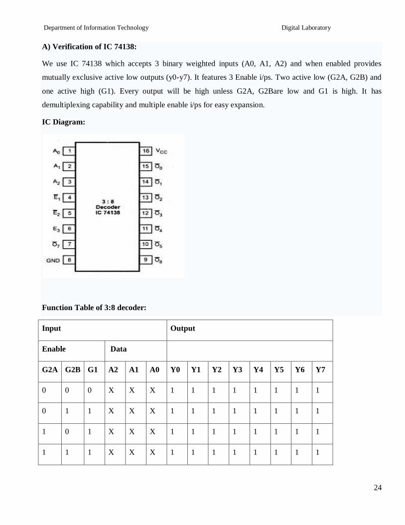
Department of Information Technology Digital Laboratory
24
A) Verification of IC 74138
We use IC 74138 which accepts 3 binary weighted inputs (A0 A1 A2) and when enabled provides
mutually exclusive active low outputs (y0-y7) It features 3 Enable ips Two active low (G2A G2B) and
one active high (G1) Every output will be high unless G2A G2Bare low and G1 is high It has
demultiplexing capability and multiple enable ips for easy expansion
IC Diagram
Function Table of 38 decoder
Input Output
Enable Data
G2A G2B G1 A2 A1 A0 Y0 Y1 Y2 Y3 Y4 Y5 Y6 Y7
0 0 0 X X X 1 1 1 1 1 1 1 1
0 1 1 X X X 1 1 1 1 1 1 1 1
1 0 1 X X X 1 1 1 1 1 1 1 1
1 1 1 X X X 1 1 1 1 1 1 1 1
Department of Information Technology Digital Laboratory
25
0 0 1 0 0 0 0 1 1 1 1 1 1 1
0 0 1 0 0 1 1 0 1 1 1 1 1 1
0 0 1 0 1 0 1 1 0 1 1 1 1 1
0 0 1 0 1 1 1 1 1 0 1 1 1 1
0 0 1 1 0 0 1 1 1 1 0 1 1 1
0 0 1 1 0 1 1 1 1 1 1 0 1 1
0 0 1 1 1 0 1 1 1 1 1 1 0 1
0 0 1 1 1 1 1 1 1 1 1 1 1 0
B) Cascading of IC 74138
The enable ip G1 active high of IC 74138 is used for cascadingfor cascading 2 ICrsquos the enable ip G1 of
first IC is connected to G1 enable ip of second IC through a NOT gate This enable ip is used as MSB
select ip line A3 the other three select input lines of both ICrsquos (A0A1A2) are also shorted to select
input lines of second IC to get single ip select lines (A0A1A2)
The ip line A3 is used to enable disable the 2 IC 74138 decoders When A3=0 first IC is enabled and
second is disabled Thus the first decoder will generate minterms from 0000 to 0111 as op and the second
decoder will generate nothing When A3=1 the enable conditions are reversed and thus second decoder
IC will generate minterms 1000 to 1111
Function Table of 416 decoder using IC 74138 (38 decoder)
Input Output
Enable Data
G2
A
G2
B
A
3
A
2
A
1
A
0
Y
0
Y
1
Y
2
Y
3
Y
4
Y
5
Y
6
Y
7
Y
8
Y
9
Y1
0
Y1
1
Y1
2
Y1
3
Y1
4
Y1
5
0 1 X X X X 1 1 1 1 1 1 1 1 1 1 1 1 1 1 1 1
Department of Information Technology Digital Laboratory
26
1 0 X X X X 1 1 1 1 1 1 1 1 1 1 1 1 1 1 1 1
1 1 X X X X 1 1 1 1 1 1 1 1 1 1 1 1 1 1 1 1
0 0 0 0 0 0 0 1 1 1 1 1 1 1 1 1 1 1 1 1 1 1
0 0 0 0 0 1 1 0 1 1 1 1 1 1 1 1 1 1 1 1 1 1
0 0 0 0 1 0 1 1 0 1 1 1 1 1 1 1 1 1 1 1 1 1
0 0 0 0 1 1 1 1 1 0 1 1 1 1 1 1 1 1 1 1 1 1
0 0 0 1 0 0 1 1 1 1 0 1 1 1 1 1 1 1 1 1 1 1
0 0 0 1 0 1 1 1 1 1 1 0 1 1 1 1 1 1 1 1 1 1
0 0 0 1 1 0 1 1 1 1 1 1 0 1 1 1 1 1 1 1 1 1
0 0 0 1 1 1 1 1 1 1 1 1 1 0 1 1 1 1 1 1 1 1
0 0 1 0 0 0 1 1 1 1 1 1 1 1 0 1 1 1 1 1 1 1
0 0 1 0 0 1 1 1 1 1 1 1 1 1 1 0 1 1 1 1 1 1
0 0 1 0 1 0 1 1 1 1 1 1 1 1 1 1 0 1 1 1 1 1
0 0 1 0 1 1 1 1 1 1 1 1 1 1 1 1 1 0 1 1 1 1
0 0 1 1 0 0 1 1 1 1 1 1 1 1 1 1 1 1 0 1 1 1
0 0 1 1 0 1 1 1 1 1 1 1 1 1 1 1 1 1 1 0 1 1
0 0 1 1 1 0 1 1 1 1 1 1 1 1 1 1 1 1 1 1 0 1
0 0 1 1 1 1 1 1 1 1 1 1 1 1 1 1 1 1 1 1 1 0
C) Implementation of Boolean function
The procedure for implementation of combinational circuit by means of a decoder and lsquoORrsquo gates requires
that the Boolean function fir the circuit be expressed in Sum of Minterms These forms can be obtained by
Department of Information Technology Digital Laboratory
27
expanding the function A decoder is then chosen which generates all the minterms of n ip variables The
ip to each OR gate are selected from the decoder outputs according to the minterms list in each function
i) F1=summ (1 3 5 7)
Truth table
Logic Diagram
ii) F2=summ (1 3 5 7111315)
Truth table
Logic Diagram
Conclusion In this way multiplexer Decoderamp its applications are studied implemented amp
tested
FAQrsquos
1What is a multiplexer
2What is a Demultiplexer
3 Enlist applications of multiplexer
Department of Information Technology Digital Laboratory
28
Regularity Content Viva-voce Timely
Submission Total
Dated Sign of
Subject
Teacher
2 4 2 2 10
Date of Performance Date of Completion
-------------------------------------------------------------------------------------------------------------------
Assignment No4
------------------------------------------------------------------------------------------------------------------
Title 3 bit updown Asynchronous and Synchronous counter using IC7476
------------------------------------------------------------------------------------------------------------------
Objective To understand design procedure of asynchronousamp Synchronous counter
------------------------------------------------------------------------------------------------------------------
Problem Statement Design (State diagram state table amp K map) and implementation of 3
bit Up and Down Asynchronous and Synchronous Counter using master slave JK flip-flop IC 7476
-----------------------------------------------------------------------------------------------------------------
Hardware Requirement
i) IC 7476 (MS-JK Flip-flop) IC 7408(Quad 2 ip AND Gate)
IC 7432 (Quad 2 ip OR Gate) and IC 7404 (Hex Inverter)
ii) Digital Trainer Kit -132
iii) Patch cords
----------------------------------------------------------------------------------------------------------------
Software Requirement Digital Work 30
------------------------------------------------------------------------------------------------------------------
Theory
Counters counters are logical device or registers capable of counting the no of states or no of clock
pulses arriving at its clock input where clock is a timing parameter arriving at regular intervals of time
so counters can be also used to measure time amp frequencies They are made up of flip flops Where the
Department of Information Technology Digital Laboratory
29
pulse are counted to be made of it goes up step by step amp the op of counter in the flip flop is decoded to
read the count to its starting step after counting n pulse incase of module counters
Types of Counters
Counter are of two types
1) Asynchronous counter
2) Synchronous counter
Asynchronous counter
A digital counter is a set of flip flop The flip flop are connected such that their combined state at any time
is binary equivalent of total no of pulses that have occurred up to that time Thus its name implies a
counter is used to count pulse A counter is used as frequency dividers To obtain waveform with
frequency that is specific fraction of clock frequency
Counter may be Asynchronous or synchronous The Asynchronous counter is also called as ripple counter
An Asynchronous counter uses T flip flop to perform a counting function The actual hardware used is
usually J-K flip flop with J amp K connected to logic1Even D flip flops may be used here
In asynchronous counter commonly called ripple counter the first flip-flop is clocked by the external
clock pulse amp then each successive flip-flop is clocked by the Q or Qrsquo output of the previous flip-flop
Therefore in an asynchronous counter the flip-floprsquos are not clocked simultaneously The input of MS-JK
is connected to VCC because when both inputs are one output is toggled As MS-JK is negative edge
triggered at each high to low transition the next flip-flop is triggered
Synchronous Counter
When counter is clocked such that each flip flop in the counter is
triggered at the same time the counter is called as synchronous counter
The gates propagation delay at reset time will not be present or we may say will not occur
1) Asynchronous Up Counter
Fig 1 shows 3bit Asynchronous Up Counter Here Flip-flop 2 act as a MSB Flip-flop and Flip-flop 0 act
as a LSB Flip-flop Clock pulse is connected to the Clock of Flip-flop 0 Output of Flip-flop 0(Q0) is
connected to clock of next flip-flop (ie Flip-flop 1) and so on As soon as clock pulse changes output is
going to change (at the negative edge of clock pulse) as a Up count sequence For 3 bit Up counter state
table is as shown below
Department of Information Technology Digital Laboratory
30
State Table
Logic diagram
Fig 1 3 Bit Asynchronous Up Counter
Hardware requirements
Gate
Flip flop
Quantity IC Quantity
MS JK 3 7476 2
2) Down Counter
Fig 2 shows 2 bit Asynchronous Down Counter Here Flip-flop 2 act as a MSB Flip-flop and Flip-flop 0
act as a LSB Flip-flop Clock pulse is connected to the Clock of Flip-flop 0 Output of Flip-flop 0 (Q0rsquo) is
Counter States Count
Q2 Q1 Q0
0 0 0 0
1 0 0 1
2 0 1 0
3 0 1 1
4 1 0 0
5 1 0 1
6 1 1 0
7 1 1 1
8 0 0 0
Department of Information Technology Digital Laboratory
31
connected to clock of next flip-flop (ie Flip-flop 1) and so on As soon as clock pulse changes output is
going to change (at the negative edge of clock pulse) as a down count sequence For 3 bit down counter
sate table is as shown below
In both the counters Inputs J and K are connected to Vcc hence J-K Flip flop work in toggle mode Preset
and Clear both are connected to logic 1
State Table
Logic diagram
Fig 2 3 Bit Asynchronous Down Counter
Hardware requirements
Counter States Count
Q2 Q1 Q0
7 1 1 1
6 1 1 0
5 1 0 1
4 1 0 0
3 0 1 1
2 0 1 0
1 0 0 1
0 0 0 0
7 1 1 1
Department of Information Technology Digital Laboratory
32
Gate
Flip flop
Quantity IC Quantity
MS JK 3 7476 2
Applications
The asynchronous counters are specially used as the counting devices
They are also used to count number of pulses applied
It also works as frequency divider
It helps in counting the number of product coming out of the machinery where product is coming out at
equal interval of time
Types of synchronous counter
1) Up counter
2) Down counter
1 3 bit Synchronous up counter
The up counter counts from 0 to7 ie(000 to 111)for this we are using MS JK flip flop In IC 74LS76 2
MS J-K flip flops are present The clock pulse is given at pin 1 amp 6 of the 1st IC amp pin 1 of 2nd IC Next
state decoder logic is designed with the help of state table
State table for synchronous up counter
Present state Next state Flip flop 3 Flip flop 2 flip flop 1
Q2 Q1 Q0 Q2 Q2 Q0 J2 K2 J1 K1 J0 K0
0 0 0 0 0 1 0 x 0 X 1 x
0 0 1 0 1 0 0 x 1 X x 1
0 1 0 0 1 1 0 x x 0 1 x
0 1 1 1 0 0 1 x x 1 x 1
1 0 0 1 0 1 x 0 0 X 1 X
1 0 1 1 1 0 x 0 1 X x 1
1 1 0 1 1 1 x 0 x 0 1 X
1 1 1 0 0 0 x 1 x 1 x 1
Department of Information Technology Digital Laboratory
33
K-Map
Q1Q0
Q2
00 01 11 10
0 0 0 1 0
1 X X X X
J2= Q1Q0
Q1Q0
Q2
00 01 11 10
0 X X X X
1 0 0 1 0
K2= Q1Q0
Q1Q0
Q2
00 01 11 10
0 0 1 X X
1 0 1 X X
J1= Q0
Q1Q0
Q2
00 01 11 10
0 X X 1 0
1 X X 1 0
K1= Q0
Department of Information Technology Digital Laboratory
34
Q1Q0
Q2
00 01 11 10
0 1 X X 1
1 1 X X 1
J0= 1
Q1Q0
Q2
00 01 11 10
0 X 1 1 X
1 X 1 1 X
K0= 1
Logic Diagram
Fig 1 3 bit Synchronous up counter
Department of Information Technology Digital Laboratory
35
2 3 bit Synchronous down counter
This is used to count from 7-0 ie(111-000)for this also 2 ICrsquos of 74LS76 are required amp hence we use 3
MS JK flip flops Here also clock is given to 1stamp 6th pin of 1st IC amp1st pin of 2nd IC enabling to apply
clock to all flip flop at a time Next state decoder logic is designed with the help of state table
State table for synchronous down counter
Present state Next state Flip flop 3 Flip flop 2 Flip flop 1
Q2 Q1 Q0 Q2 Q1 Q0 J2 K2 J1 K1 J0 K0
1 1 1 1 1 0 X 0 X 0 X 1
1 1 0 1 0 1 X 0 X 1 1 X
1 0 1 1 0 0 X 0 0 X X 1
1 0 0 0 1 1 X 1 1 X 1 X
0 1 1 0 1 0 0 X X 0 X 1
0 1 0 0 0 1 0 X X 1 1 X
0 0 1 0 0 0 0 X 0 X X 1
0 0 0 1 1 1 1 X 1 X 1 X
K-Map
Q1Q0
Q2
00 01 11 10
0 1 0 0 0
1 X X X X
J2= Q1Q0
Q1Q0
Q2
00 01 11 10
Department of Information Technology Digital Laboratory
36
0 X X X X
1 1 0 0 0
K2= Q1Q0
Q1Q0
Q2
00 01 11 10
0 1 0 X X
1 1 0 X X
J1= Q0
Q1Q0
Q2
00 01 11 10
0 X X 0 1
1 X X 0 1
K1= Q0
Q1Q0
Q2
00 01 11 10
0 1 X X 1
1 1 X X 1
J0= 1
Q1Q0
Q2
00 01 11 10
0 X 1 1 X
1 X 1 1 X
K0= 1
Department of Information Technology Digital Laboratory
37
Logic Diagram
Fig 2 3 bit Synchronous down counter
Uses
1 Specially used as the counting devices
2 Used in frequency divider circuit
3 Used in digital voltmeter
4 Used in counter type A to D converter
5 Used for time measurement
6 It helps in counting the no of product coming out from machinery where product is coming out
at equal interval of time
Conclusion
Up and down counters are successfully implemented the counters are studied amp op are checked The
state table is verified
PRACTICE ASSIGNMENTS EXERCISE MODIFICATIONS
1 Design amp implement 2 bit controlled synchronous counter
2 Designamp implement 4 bit controlled synchronous counter
3 Designamp implement truncated synchronous up or down counter
FAQrsquos with answers
1 What do you mean by Counter
A Counter is a register capable of counting the no of clock pulses arriving at its
clock inputs Count represents the no of clock pulses arrived A specified
sequence of states appears as the counter output
Department of Information Technology Digital Laboratory
38
2 What are the types of Counters Explain each
There are two types of counters as Asynchronous Counter and Synchronous Counter
Asynchronous Counter In this counter the first flip-flop is clocked by the external clock pulse
and then each successive flip-flop is clocked by the Q or Qrsquo op of the previous flip-flop Hence in
Asynchronous Counter flip-flops are not clocked simultaneously and hence called as Ripple
Counter Synchronous Counter In this counter the common clock input is connected to all the
flip-flops simultaneously
3 What do you mean by pre-settable counters
A counter in which starting state is not zero can be designed by making use of the
preset inputs of the flip flops This is referred to as loading the counter
asynchronously This is referred to as pre-settable counter
4 What are the applications of synchronous counters
Digital clock
Frequency divider circuits
Frequency counters
Used in analog to digital converters
5 What are the advantages of synchronous counters over asynchronous counters
Propagation delay time is reduced
Can operate at a much higher frequency than the asynchronous counters
6 Ring counter is an example of synchronous counters or asynchronous counter
Synchronous counter Since all the flip flops are clocked simultaneously
7 Twisted Ring (Johnsonrsquos) counter is an example of synchronous counters or asynchronous
counter
Synchronous counter Since all the flip flops are clocked simultaneously
8 What is the difference between ring counter and twisted ring counter
In ring counter pulses to be counted are applied to a counter it goes from state to state and the
output of the flip flop s in the counter is decoded to read the count Here the uncomplimentary
output (Q) of last flip flop is fed back as an input to first flip flop Ring counters are referred as
MOD lsquoNrsquo counters
Department of Information Technology Digital Laboratory
39
But in Twisted ring counter the complimentary output (Q bar) of last flip flop is fed back as an
input to first flip flop Twisted Ring counters are referred as MOD lsquo2Nrsquo counters
9 What are the applications of ring counters
Ring counter outputs are sequential non-overlapping pulses which are useful for control state
counters Used in stepper motor this requires pulses to rotate it from one position to the next Used
as divide by lsquoNrsquo ((MOD lsquoNrsquo) counters
10 What are the applications of ring counter twisted ring counters
Used as divide by lsquo2Nrsquo ((MOD lsquo2Nrsquo) counters
Used for control state counters
Used for generation of multiphase clock
11 List the Synchronous Counter ICs
IC 74160 Decade Up Counter
IC 74161 4 bit binary Up Counter
IC 74162 Decade Up Counter
IC 74163 4 bit binary Up Counter
IC 74168 Decade UpDown Counter
IC 74169 4 bit Binary UpDown Counter
IC 74190 Decade UpDown Counter
IC 74191 4 bit Binary UpDown Counter
IC 74192 Decade UpDown Counter
IC 74193 4 bit Binary UpDown Counter
Department of Information Technology Digital Laboratory
40
Regularity Content Viva-voce Timely
Submission Total
Dated Sign of
Subject
Teacher
2 4 2 2 10
Date of Performance Date of Completion
-------------------------------------------------------------------------------------------------------------------
Assignment No 5
-------------------------------------------------------------------------------------------------------------------------------
Title Design and implementation of Module lsquonrsquo counter with IC7490 and IC 74191
-----------------------------------------------------------------------------------------------------------------------------
Objective To know difference between regular amp truncated counter as well as binary ampBCD Counter
--------------------------------------------------------------------------------------------------------------------------------
Problem Statement To design and implement mod - 10 mod ndash 7 mod - 99 asynchronous BCD
counter using IC 7490 and to design and implement up down mod - n Binary counter using IC 74191
-----------------------------------------------------------------------------------------------------------------
Hardware Requirement
i) IC 7490 IC 74191 basic gates
ii) Digital Trainer Kit -1
iii) Patch cords
----------------------------------------------------------------------------------------------------------------
Software Requirement Digital Work 30
------------------------------------------------------------------------------------------------------------------
Theory
Part A ndash IC 7490
IC 7490 is a TTL MSI (medium scale integration) decade counter It contains 4 master slave flip flops
internally connected to provide MOD-2 ie divide by 2 and MOD-5 ie divide by 5 counters MOD-2 and
Mod-5 counters can be used independently or in cascading
Department of Information Technology Digital Laboratory
41
It is a 4-bit ripple type decade counter The device consists of 4-master slave flip flops internally
connected to provide a divide by two and divide by 5 sections Each section has a separate clock ip to
initiate state changes of the counter on the high to low clock transition
Since the op from the divide by 2 section is not internally connected to the succeeding stages The device
may be operated in various counting modes In a BCD counter the CP1 input must be externally connected
to QA op The CP0ip receives the incoming count producing a BCD count sequence It is also provided
with additional gating to provide a divide by 2 counter and binary counter for which the count cycle length
is divide by 5 The device may be operated in various counting modes
There are 2 reset inputs R0(1) and R0(2) both of which need to be connected to the lsquologic 1rsquo for clearing all
flip flops Two set inputs Rg(1) and Rg(2) when connected to logic 1 are used for setting counter to 1001
(BCD 9)
Pin out of IC 7490
Fig Pin configuration of IC7490
Table 1-pin name and description of IC7490
Pin name Description
Input B This is clock input to the internal MOD-5 ripple counter which is negative
edge triggered
R0(1)R0(2) Gated zero reset inputs
Department of Information Technology Digital Laboratory
42
R9(1)R9(2) These are gated set to nine inputs
QDQCQB Output of internal MOD-5 counter with QD as MSB
QA Output of internal MOD-2 counter with QA as LSB
Input A Clock input to FF-A which is negative edge triggered
Functional Table for IC7490
Reset inputs Output
R0(1) R0(2) R9(0) R9(1) QD QC QB QA
1 1 0 X 0 0 0 0
1 1 X 0 0 0 0 0
X X 1 1 1 0 0 1
X 0 X 0 COUNTER
0 X 0 X COUNTER
0 X X 0 COUNTER
X 0 0 x COUNTER
Department of Information Technology Digital Laboratory
43
Basic internal Structure of IC 7490
Function Table of MOD-5 counter
Design of MOD-10 counter using IC 7490
The QA op the first flip flop is connected to the input B which is clock ip of internal MOD-5 ripple
counter Due to cascading of Mod-2 and Mod-5 counters the overall configuration the decade counters
count from 0000 to 1001 After 1001 mod-5 resets to 0000 and next count after 1001 is 0000
When QA op is connected to B ip we have the Mod-2 counter followed by Mod-5 counter The
count sequence obtained is shown in the table It may be noted that QA changes from 0 to 1 the state of
InputB clock Output
Count QD QC QB
0 0 0 0
0 0 1 1
0 1 0 2
0 1 1 3
1 0 0 4
Department of Information Technology Digital Laboratory
44
Mod-5 counter doesnrsquot change whereas when QA changes from 1 to 0 the Mod-5 counter goes to the next
state
Logic DiagramMOD-10 counter using IC 7490
5 Modulus n Counter
Function table
Ip clock
Output
Count QD QC QB QA
0 0 0 0 0
0 0 0 1 1
0 0 1 0 2
0 0 1 1 3
0 1 0 0 4
Department of Information Technology Digital Laboratory
45
Design of Mod-7 Counter using IC 7490
Mod-7 counter counts through seven states from 0 to 6 counters and it should reset as soon as the
count becomes 7 The op of reset logic should be 1 corresponding to invalid states The reset logic op
should be applied to pin 2 and 3
Truth Table of Reset Logic
0 1 0 1 5
0 1 1 0 6
0 1 1 1 7
1 0 0 0 8
1 0 0 1 9
QD QC QB QA Y
0 0 0 0 0
0 0 0 1 0
0 0 1 0 0
0 0 1 1 0
0 1 0 0 0
0 1 0 1 0
0 1 1 0 0
0 1 1 1 1
1 0 0 0 1
1 0 0 1 1
Department of Information Technology Digital Laboratory
46
Logic Diagram Mod 7 Counter using IC 7490
Function table
Ip clock
Output
Count QD QC QB QA
0 0 0 0 0
0 0 0 1 1
0 0 1 0 2
0 0 1 1 3
0 1 0 0 4
0 1 0 1 5
0 1 1 0 6
Department of Information Technology Digital Laboratory
47
Design of Mod-99 using IC 7490
For Mod-99 two IC 7490rsquos will be required Hence to implement a divide by 99 counter we have
to use two decade counters ICrsquos A divide by 99 counter counts 99 states from 0 to 98 and the counter
should reset as soon as the count becomes 99 So in order to reset the counter of 99 connect the Q op
which are equal to 1 in the count of 99 to an lsquoAndrsquo gate amp then connect and op to the reset ip of both
ICrsquos
MOD-100 Counter-
MOD-100 counter can be obtained by cascading two decade counter ICrsquos
Each IC gives divide by 10 counts Hence 2 ICs will give 1010=100 counts
Clock is applied to the input A of IC 7490 the Q1 output is connected to B input etc
For cascading the QD output of the first IC is connected to the input A of second IC Thus QD of
IC-(1) acts as clock input to IC-(2)
The Ro (1) Ro(2) R9(1) R9(2) inputs of both ICs are connected to ground so as to make them
inactive
The total count provided by the two counters varies from 00 to 99 decimal that means 100 states
Hence it is a MOD-10 counter
Impleacutementations
FigureMOD-100 counters using IC 7490
Department of Information Technology Digital Laboratory
48
B) IC 74191 ndash Theory
IC74191 is 4-bit binary synchronous reversible up down counter It contains 4 master slave flip flops
with internal gating and steering logic to provide asynchronous reset and synchronous count updown
operations its asynchronous parallel capability permits the counter to be preset to any desire number D0
to D3 are the parallel data inputs Information present on the parallel data inputs D0 to D3 is loaded into
the counter and appears on the output when the load PLinput is lowThisoperation overrides the counting
function Counting is inhabited by the high level on the enable G input when G input is low internal state
changes are initiated synchronously by the low to high transitions of the clock inputs the updown input
signal determines the direction of input
Function Table
Operating
mode
Inputs Outputs
PL UD G CLK Dn
Parallel
load L X X X L L
L X X X H H
Count up H L 0 uarr X Count up
Count
down H H 0 uarr X
Count
down
Hold(No
change) H X H X X No change
Pin details ndash
D0 to D3 input lines PL parallel load
G is Enable input ndash enabling the counting
Q0 to Q3 output lines
Downup determines the direction of counting
Clk clock input for counter
Terminal Count Max(1111) min(0000) For these states signal goes high for 1clock pulse
Ripple clock Clock input for next higher state
Department of Information Technology Digital Laboratory
49
Pin Diagram IC 74191
Up counter- Truth Table
Clk
Pulses QA QB QC QD
0 0 0 0 0
1 0 0 0 1
2 0 0 1 0
3 0 0 1 1
4 0 1 0 0
5 0 1 0 1
6 0 1 1 0
7 1 1 1 1
8 1 0 0 0
9 1 0 0 1
10 1 0 1 0
11 1 0 1 1
12 1 1 0 0
13 1 1 0 1
Department of Information Technology Digital Laboratory
50
14 1 1 1 0
15 1 1 1 1
Logic Diagram
Steps-
Connect the circuit as shown above
Apply clock ip to pin no14
Connect UD to GND
Verify the output according to truth table
Logic diagram of down counter
Steps-
Connect the circuit as shown above
Apply clock ip to pin no14
Connect UD to VCC
Verify the output according to truth table
UD D3 D2 D1 D0 PL
Clock IC 74191
G RC
MAX MIN
Q3 Q2 Q1 Q0 TC
vcc
NC
NC
Outputs
no connection
vcc
Department of Information Technology Digital Laboratory
51
With the help of IC74191 we can implement truncated updown counter by using following logic ndash
Connect data input line to particular count you want to load
According to requirement make Truth table
Draw the K-map
Find out Boolean expression
Draw the logic diagram and that is the combinational logic for your count and apply the output of
that circuit to PL
According to requirement we get the UP and down counting
5 Modulus n Counter
Presettable updown counter
Mod 11 counter
Implementation of presetttable mod updown counter using IC- 74LS191
1 Load Data on data lines D0 to D3 (0101)
2 Counter will go through the states from 0101 0110hellip1111 in up counter and 0101 to 0000 in
down counter
Combinational Circuit
CLOCK D3 D2 D1 D0
TC
U D 74191 RC
G PL
Updown Q3 Q2 Q1 Q0 PL
Q3 Q2 Q1 Q0
Preset Count
Department of Information Technology Digital Laboratory
52
3 The logic circuit should be designed in such a way that only when all the outputs are high output
of the reset circuit should be low and the counter should jump to state 5 It should again start
counting from 0101 to 0000
State Table
Down Counter UP Counter
IC 74191 is 4 bit counter Thus it counts 0000 to 1111 different 16 states For MOD11 counter we require
different 11 states so 5 steps must be skipped from 16 states We get MOD11 by presetting counter to
value 5
Assignment Question
Design and Implement MOD 7 MOD 10 and MOD 12 using IC 74191
FAQs
1 What do you mean modulus counter
Counter
state Clock
pulse
Q3 Q2 Q1 Q0
1 0 1 0 1
2 0 1 1 0
3 0 1 1 1
4 1 0 0 0
5 1 0 0 1
6 1 0 1 0
7 1 0 1 1
8 1 1 0 0
9 1 1 0 1
10 1 1 1 1
11 1 1 1 1
Counter state
Clock pulse
FF outputs
Q3 Q2 Q1 Q0
1 0 1 0 1
2 0 1 0 0
3 0 0 1 1
4 0 0 1 0
5 0 0 0 1
6 0 0 0 0
7 0 1 0 1
Department of Information Technology Digital Laboratory
53
It represents the number of possible states of counter
2 How will you use the 7490 IC to design symmetrical divide by 10 frequency counter
The divide by 5 circuit followed by divide by 2 circuit will give symmetrical output
3Where counters are used Give real life example of counter
Modulus n Counter
Binary counter ndash An N stage counter that recycles after 2 Ncount The count proceds in specified binary
sequence Counter Presetable- A counter which can be set to a desired value before the start of the
counting UPDown counter ndash A counter that can count in both up and down direction depending upon a
control input
Department of Information Technology Digital Laboratory
54
Regularity Content Viva-voce Timely
Submission Total
Dated Sign of
Subject
Teacher
2 4 2 2 10
Date of Performance Date of Completion
-------------------------------------------------------------------------------------------------------------------
Assignment No6
------------------------------------------------------------------------------------------------------------------
Title Sequence Generator
------------------------------------------------------------------------------------------------------------------
Objective To understand sequence generator one of the sequential circuit
-------------------------------------------------------------------------------------------------------------------
Problem Statement Design (State Diagram State Table K Map) and implementation of Sequence
Generator using Shift Register IC 74194
-----------------------------------------------------------------------------------------------------------------
Hardware Requirement
i) IC 741947408 (AND-gate) 7432 (OR-gate)
ii) Digital Trainer Kit -1
iii) Patch cords
----------------------------------------------------------------------------------------------------------------
Software Requirement Digital Work 30
------------------------------------------------------------------------------------------------------------------
Theory
Part A Sequence Generator with Flip flop
A sequential circuit which generates a prescribed sequence of bits in synchronism with a clock is referred
to as a sequence generator These pulse trains or sequence of bits can be used to open valves close gates
turn on lights and turn off machines and other variety of jobs
Department of Information Technology Digital Laboratory
55
For the design of sequence generator we first determine the required no of flip flops and the logic circuit
for the next state decoder
No of flip flops required to generate particular sequence can be determined as follows
1) Find the no of 1rsquos in the sequence
2) Find the no of 0rsquos in the sequence
3) Take the maximum out of two
4) If N is the required no of flip flops choose minimum value of lsquonrsquo to satisfy equation given below
Max (0rsquos 1rsquos) le 2n-1
The sequence generator can be classified as
1) sequence generator without bushing
2) sequence generator with bushing
The aim in this experiment is to design a sequence generator to generate a sequence of bit ie 10101
Part B Sequence Generator using Shift Register IC 74194
IC 74194 4 bit bidirectional Shift Register
This bidirectional shift register is designed to incorporate virtually all the features a system designer may
want in a shift register they feature Parallel inputs parallel outputs right shift left shift serialinputs
operating mode control inputsand a direct overriding clear line The register has four distinct modes of
operationsnamely
1 Parallel load
2 Shift right (in the direction QA towards QD)
3 Shift left (in the direction QD towards QA)
4 Inhibit clock (do nothing)
Synchronous parallel loading is accomplished by applying the four bits of data and taking both
mode control inputs S0 and S1High The data is loaded in to the associated flip-flops and appear
at the outputs after positive transition of the clock input During loading serial data flow is
inhibited
Shift right is accomplished synchronously with the rising edge of the clock pulse when S0 is High
and S1 is Low Serial data for this mode is entered at the shift right data input When S0 is Low
and S1 is High data shifts left synchronously and new data is entered at the shift left serial input
Clocking of the flip flop is inhibited when both mode control inputs are LOW
Department of Information Technology Digital Laboratory
56
Mode Control Input Operation
S1 S0
0 0 Clock Inhibit
0 1 Shift right
1 0 Shift Left
1 1 Parallel loading
Function Table of IC 74194
Design
The minimum number of flip-flops N required to generate a sequence of length S is given by S
le 2N ndash 1
In this case S=7 therefore the minimum value of N which may generate in this sequence is 3
However it is not guaranteed to lead to a solution If the given sequence leads to seven distinct
states then only three flip flops are sufficient otherwise we have to increase the number of flip
flops We write the states of circuit as given in table 1 The prescribed sequence is listed under QA
and the sequence listed under QB and QC are the same sequence delayed by one and two clock
pulses respectively From the table we observe that all the states are not distinct which means N=3
is not sufficient Next we assume that N=4 and prepare table 2 The last column gives the required
serial input for getting the desired change of state when a clock pulse is applied This is obtained
by assuming D type flip flop and looking at the QA output For example at the falling edge of first
clock pulse QA=1 The second clock pulse must result in QA=1 which requires its D input to be 1
In the same manner all the entries in column Y are determined
Table 1 State Assignment Table of Sequence Generator (N=3)
Number of Clock
Pulses
Flip Flop Inputs States
QA QB QC
1 1 1 1 7
2 1 1 1 7
3 0 1 1 3
4 1 0 1 5
Department of Information Technology Digital Laboratory
57
5 0 1 0 2
6 1 0 1 5
7 1 1 0 6
Excitation table of D Flip-Flop
Present State Qn Next State Qn+1 Flip-Flop Input D
0 0 0
0 1 1
1 0 0
1 1 1
Table 2State Assignment Table of Sequence Generator (N=4)
Number of Clock
Pulses
Flip Flop Inputs States
Y
Serial ip QA QB QC QD
1 1 1 1 0 14 1
2 1 1 1 1 15 0
3 0 1 1 1 7 1
4 1 0 1 1 11 0
5 0 1 0 1 5 1
6 1 0 1 0 10 1
7 1 1 0 1 13 1
K-Map Simplification
Department of Information Technology Digital Laboratory
58
00 01 11 10
00 X X X X
01 X 1 1 X
11 X 1 0 1
10 X X 0 1
Y= QArsquo + QBrsquo + QCrsquo = QAQBQC
LOGIC DIAGRAM
HARDWARE REQUIREMENTS
Sr no ICs Description Quantity
11 74194 4 bit bidirectional universal shift register 16ktr`
2 7410 3 input NAND Gate 1
Department of Information Technology Digital Laboratory
59
Conclusion In this way sequence generator using JK flip flips amp shift register is designed and
implemented
Enhancements Modifications ndash Sequence generator can also be implemented with shift register instead
of flip flops Use IC 7495 universal shift register IC and try to implement sequence generator
FAQs
1 What is sequential logic circuit
A sequential logic circuit consists of a memory elements in addition to
combinational circuit Its output at any instant of time depends upon
the present input as well as present state of memory element
2 What is meant by delay line
It is used to introduce time delays in digital signals
3 What is meant by following terms
a) Synchronous preset b) Asynchronous preset
c) Synchronous clear d) Asynchronous clear
a)Preset operation is synchronised with the clock
b)Preset operation is independent of the clock
c) clear is performed in synchronous with clock
d) clear is performed independent with clock
4 Is asynchronous counter faster than synchronous counter
In a synchronous counter the time required for change of any state is same and is equal to delay
time of one flip flop where as in asynchronous counter all flip flops are not clocked
simultaneously hence time required is not same
5 What is mean by lockout in counter
In a counter design for a fewer state than the maximum possible state some time it may so happen
that counter enters in unused state and goes from one unused state to another unused state and
never comes to used state
6 What is mean by state table
Department of Information Technology Digital Laboratory
60
It consists of complete information about present state and next state and outputs of a sequential
system
7 What is mean by state diagram
The information available in a state table can be represented as graphically the graphical
representation is known as state diagram
8 What is the advantage of state reduction in the design of sequential circuit
It reduces the number of flip flops
9 What is meant by excitation table
This gives information about what should be the flip flop inputs if outputs are specified before and
after the clock pulse
10 How many flip flops are required to design sequence generator using Counters
max (0rsquoS1rsquoS) in a given sequence lt= 2(N - 1)
Where N = Number of flip flops
11 How many flip flops are required to design sequence generator using shift registers
Slt= 2N - 1
Where N=Number of flip flops
S= Length of sequence
12 What is Lock out condition How it is avoided
When counter enters into one of the invalid state and after application of pulses remains in invalid
states only i e counter gets locked into invalid state amp this is called as lock out Lock out can be
avoided by providing bushing to all the invalid states in such a way that after application of one or
more clock pulses counter will fall into one of the valid state
Department of Information Technology Digital Laboratory
61
Regularity Content Viva-voce Timely
Submission Total
Dated Sign of
Subject
Teacher
2 4 2 2 10
Date of Performance Date of Completion
-------------------------------------------------------------------------------------------------------------------
Assignment No7
------------------------------------------------------------------------------------------------------------------
Title Multiplexer using Data flow modeling and structural modeling
------------------------------------------------------------------------------------------------------------------
Objective To learn data flow modeling style Its uses and different types of declarations with some
different types of circuits Structure of VHDL program is well discussed with this modeling style
-------------------------------------------------------------------------------------------------------------------
Problem Statement 41 multiplexer using data flow amp structural modeling -
----------------------------------------------------------------------------------------------------------------
Hardware Requirement - NA
----------------------------------------------------------------------------------------------------------------
Software Requirement Xilinx
------------------------------------------------------------------------------------------------------------------
Theory
Data flow style-
In this type of design the view of data as flowing from input to output through a design
An operation is defined in terms of a collection of data transformation expressed as concurrent
statement Each of the statement can be activated when any of its input signal changes its value While
these statements describe the behavior of the circuit a lot of information about its structure can be
extracted from the description as well
Data flow modeling has a set of concurrent assignment statements In the data flow level of abstraction we
describe how information is passed in the circuit The built in operators in VHDL are used in expression
such as AND OR XOR NOT etc
Department of Information Technology Digital Laboratory
62
INPUT
Two select lines S1S0
Four data lines D0 D1 D2 D3
OUTPUT
One output line Y
Functional block diagram of 41 Mux
Fig 41 Multiplexer using Data flow modeling
Function table of 41 Mux
Enable S1 S0 A B C D Y
1 X X X X X X 0
0 0 0 A X X X A
0 0 1 X B X X B
0 1 0 X X C X C
0 1 1 X X X D D
Design steps
Click on Xilinx ISE 92i
Create New project from file menu Ensure top level source is HDL
Select family of devices (usually spartan2E or 3)
Department of Information Technology Digital Laboratory
63
Ensure preferred language is VHDL
Click new source which shows you project details device details
and Synthesis and simulator tools
After finishing project create new source by right clicking in project name with VHDL
module
Complete ports name directions and bus Ensure architecture name is behavioral
After that we will get design summary and detailed reports
Close design summary
Create your code with given modeling style
Go to process window and synthesis to check if any error is there in code Check syntax and
view RTL schematic
Create new source to simulate the code
Right click on source name and create test bench waveform with proper name Ensure the
project is same
Click on combinational circuit in initial timing wizard
Select test bench wave in source window Apply inputs to wave diagram Ensure you are in
behavioral simulation
Go to process box Click on Xilinx ISE simulator and simulate the model See results
RTL Schematic
Department of Information Technology Digital Laboratory
64
Timing Diagram
FAQrsquos
1 What are the different kinds of data objects in VHDL code
Ans data object may be any value or number still some signal data objects and bit and bit_vector
types of these are available in VHDL STD_LOGIC and STD_LOGIC_VECTOR types are used
widely in programming
2 What do you mean by signal
Ans signal is a data object represents logic signals or wires in a circuit There are three places in
which signals can be declared in VHDL code in an entity declaration in the declarative section of
architecture and in declarative section of package
3 What are different signal types
Ans BIT BIT_VECTOR STD_LOGIC STD_LOGIC_VECTOR STD_ULOGIC SIGNED
UNSIGNED INTEGER ENUMERATION and BOOLEAN
4 What is an entity
Ans a circuit or sub circuit described with VHDL code is called a design entity
5 Explain structure of an entity
Ans it has two main parts the entity declaration which specifies the input and output signals for
entity and the architecture which gives circuit details
Department of Information Technology Digital Laboratory
65
6 How will you declare a package with component Explain structure
The general form of package declaration is as shown in diagram
PACKAGE package_name IS
[TYPE declarations]
[SIGNAL declarations]
[COMPONENT declarations]
END package_name
Entity
Declaration Architecture
Department of Information Technology Digital Laboratory
66
Regularity Content Viva-voce Timely
Submission Total
Dated Sign of
Subject
Teacher
2 4 2 2 10
Date of Performance Date of Completion
-------------------------------------------------------------------------------------------------------------------
Assignment No8
------------------------------------------------------------------------------------------------------------------
Title Full Adder using Behavioral and Structural modeling
------------------------------------------------------------------------------------------------------------------
Objective To learn structural modeling style Its uses and different types of declarations with some
different types of circuits Structure of VHDL program is well discussed with this modeling style
-------------------------------------------------------------------------------------------------------------------
Problem Statement Full adder using behavioral amp structural modeling
-----------------------------------------------------------------------------------------------------------------
Hardware Requirement - NA
----------------------------------------------------------------------------------------------------------------
Software Requirement Xilinx
------------------------------------------------------------------------------------------------------------------
Theory
Structural style-
A digital electronic system can be described as a module with inputs andor outputs The electrical values
on the outputs are same functions of the values of inputs The example of it is as shown The NAND gate
has 2ips AampB amp an output y Using VHDL terminology we call the NAND2 design entity amp the inputs
amp outputs are called ports 1 way of describing the function of NAND2 is to describe how it is composed
of sub modules AND amp INVERTER Each of the Sub modules is an instance of some entity amp ports of the
instances are connected using signals Structural modeling has a set of interconnected component
Structure can be used to create a very low level description of a circuit or a very high level description
Department of Information Technology Digital Laboratory
67
In a gate level description of a circuit for example components such as basic logic gates amp FFs might be
connected in some logical stricture to create the circuit This is what is often called a net list
Structure of structural modeling
Functional block diagram of Full Adder
architectureNetlistofHalf_Adderis
-- component with locals
componentMyXorport (A_XorB_Xor in BIT
Z_Xor out BIT)
end component
-- component with locals
componentMyAndport (A_AndB_And in BIT
Z_And out BIT)
end component
begin
Xor1 MyXorport map (X Y Sum)
-- instance with actuals
And1 MyAndport map (X Y Cout)
-- instance with actuals
end
Department of Information Technology Digital Laboratory
68
Function table of Full Adder
A B Cin SUM CARRY
0 0 0 0 0
0 0 1 1 0
0 1 0 1 0
0 1 1 0 1
1 0 0 1 0
1 0 1 0 1
1 1 0 0 1
1 1 1 1 1
Sum = Σm(1 2 4 7)
Carry= Σm(3 5 6 7)
Design steps
Click on Xilinx ISE 92i
Create New project from file menu Ensure top level source is HDL
Select family of devices (usually spartan2E or 3)
Ensure preferred language is VHDL
Click new source which shows you project details device details
and Synthesis and simulator tools
After finishing project create new source(full adder) by right clicking in project name with
VHDL module
Complete ports name directions and bus Ensure architecture name is behavioral
After that we will get design summary and detailed reports
Close design summary
Click new source which shows you project details device details
and Synthesis and simulator tools
After finishing project create new source(half adder) by right clicking in project name with
VHDL module
Complete ports name directions and bus Ensure architecture name is behavioral Names
should be same as previous inputs
Department of Information Technology Digital Laboratory
69
After that we will get design summary and detailed reports
Close design summary
Create your code for half adder with given modeling style
After that go to process window Click on design utilities
View HDL instantiation code of half adder
Copy component part of half adder in architecture block of full adder Copy instantiation
template twice after begin as we require two half adders to construct full adder (structural
modeling) Name them differently (eg ha1 or ha2)
Create signals as per the logic Complete code of full adder
Go to process window and synthesis to check if any error is there in code Check syntax and
view RTL schematic
Create new source to simulate the code
Right click on source name and create test bench waveform with proper name Ensure the
project is same
Click on combinational circuit in initial timing wizard
Select test bench wave in source window Apply inputs to wave diagram Ensure you are in
behavioral simulation
Go to process box Click on Xilinx ISE simulator and simulate the model See results
RTL Schematic
Timing Diagram
Department of Information Technology Digital Laboratory
70
INPUT
Three inputs A B Carry (previous)
OUTPUT
Two outputs Sum Carry
FAQrsquos
1 What do you mean by structural style
Ans in this type of code a circuit is described in hierarchical fashion by connecting together sub
circuits
2 Explain IF statement with example
Ans The general form of an IF statement is as follws
IF Sel=rsquo0rsquo THEN
Flt=x1
ELSE
Flt=x2
END IF
Department of Information Technology Digital Laboratory
71
3 Explain declaration and instantiation process in VHDL
Ans first declare a small vhdl code in formal way Eg half adder Define project name is full adder
And simply copy instantiation template in main source code Define how many times you want to
declare this template Give separate names for those
4 What is STD_LOGIC_VECTOR
Ans It is standard data object added to VHDL standard in IEEE 1164 It provides more flexibility
than the Bit type
5 Explain difference between concurrent and sequential statements
Ans Concurrent statements define interconnected processes and blocks that together describe a designrsquos
overall behavior or structure They can be grouped using block sstatement Groups of blocks can also be
partitioned into other blocks At this same level a VHDL component can be connected to define signals
within the blocks
It is a reference to an entity A process can be a single signal assignment statement or a series of
sequential statements (SS) Within a process procedures and functions can partition the sequential
statements
PRACTICE ASSIGNMENTS
1 Implement half adder using data flow modeling
2 Implement Full Adder using behavioral modeling
3 Implement 3 bit magnitude comparator using a 3 bit adder
4 Implement half sub tractor using data flow modeling
5 Write VHDL code for Full Subtractor
Department of Information Technology Digital Laboratory
72
Regularity Content Viva-voce Timely
Submission Total
Dated Sign of
Subject
Teacher
2 4 2 2 10
rsquozaDate of Performance Date of Completion
-------------------------------------------------------------------------------------------------------------------
Assignment No9
------------------------------------------------------------------------------------------------------------------
Title Simulation of 3 bit Connter using Behavioral modeling
------------------------------------------------------------------------------------------------------------------
Objective To learn behavioral modeling style Its uses and different types of declarations with some
different types of circuits Structure of VHDL program is well discussed with this modeling style
-------------------------------------------------------------------------------------------------------------------
Problem Statement 3 bit controlled up down synchronous counter with preset amp clear
-----------------------------------------------------------------------------------------------------------------
Hardware Requirement -NA
----------------------------------------------------------------------------------------------------------------
Software Requirement Xilinx
------------------------------------------------------------------------------------------------------------------
Theory
Behavioral style-
Highest level of abstraction supported in VHDL is called the behavior level of abstraction In it we have
for loop while loop If then else case ampvariable assignment The statements are enclosed in a PROCESS
block amp are executed sequentially
In it circuit is described in terms of its operation overtime
In behavioral description the concept of time may be expressed precisely with actual delays between
related events (such as the propagation delays within gates amp on wires) or it may be simply an ordering of
operation that are expressed sequentially (such as in a functional description of a FF)
Department of Information Technology Digital Laboratory
73
A behavioral design method defines a circuit in terms of text language rather than a schematic of
interconnected symbols
Behavioral design is a technology independent text based design that incorporates high level
functionality amp high level information flow
Structure of Behavioral modeling
Functional block diagram of 3 bit controlled up down synchronous counter with preset amp clear
Function table of 3 bit controlled up down synchronous counter with preset amp clear
Design steps
Click on Xilinx ISE 92i
Create New project from file menu Ensure top level source is HDL
Select family of devices (usually spartan2E or 3)
Ensure preferred language is VHDL
Click new source which shows you project details device details
and Synthesis and simulator tools
After finishing project create new source by right clicking in project name with VHDL
module
Complete ports name directions and bus Ensure architecture name is behavioral
After that we will get design summary and detailed reports
Close design summary
Create your code with given modeling style
Go to process window and synthesis to check if any error is there in code Check syntax
and view RTL schematic Create new source to simulate the code
Department of Information Technology Digital Laboratory
74
Right click on source name and create test bench waveform with proper name Ensure the
project is same
Click on combinational circuit in initial timing wizard
Select test bench wave in source window Apply inputs to wave diagram Ensure you are in
behavioral simulation
Go to process box Click on Xilinx ISE simulator and simulate the model
RTL Schematic
Timing Diagram
INPUT
Clock Preset Clear
OUTPUT
Three output lines
FAQrsquos
1 Explain the structure of behavioral modeling
2 What are the differences between behavioral and structural modeling
Ans Behavioral descriptionof a circuit is the highest level of abstraction in VHDL Here the
circuit is described in terms of it operation with respect to time All operations are in one level of
code The operations are described in a way that the designer of a sequential circuit infers a
register
Structural description on the other hand is a circuit description in terms of its components
it can either create a low level description much like a hierarchy in a block diagram Whenever
you see a component instantiated in a code that code employs structural description of the circuit
The components are connected in the form of a netlist This is for better manageability and
reusability
3 What are the differences between behavioral and data flow modeling
Department of Information Technology Digital Laboratory
75
Ans Behavioral ndash describes how the output is derived from the inputs using structured
statements
Dataflow ndash describes how the data flows from the inputs to the output most often
using NOT AND and OR operations
4 What do you mean by process statement
Ans The process statement begins with the PROCESS keyword followed by a parenthesized list
of signals called the sensitivity list It operates on selected and conditional statements
5 Explain syntax of process statement
Ans BEGIN
Process( sensitivity list)
END process
PRACTICE ASSIGNMENTS
1 Implement 3 bit asynchronous up counter using behavioral modeling
2 Implement 3 bit asynchronous down counter using behavioral modeling
3 Implement 3 bit synchronous down counter using behavioral modeling
End
Department of Information Technology Digital Laboratory
76
Pin Diagrams
7400 Quad 2-Input NAND Gate
7402 Quad 2-Input NOR Gate
7404 Not Gates
7408 Quad 2-Input AND Gates
7432 Quad 2-Input OR Gate
7486 Quad 2-Input Exclusive-OR Gate
Department of Information Technology Digital Laboratory
77
7483 4 bit Binary Adder
7490 Decade and Binary Counters
74138 38 Decoder
Department of Information Technology Digital Laboratory
78
74153 Dual 41 Multiplexer
74191 Synchronous UpDown 4 bit Binary counter with Mode Control
Department of Information Technology Digital Laboratory
79
74194 Universal Shift Register
7476 Dual Master-Slave J-K Flip-Flops
- Part B Sequence Generator using Shift Register IC 74194
-
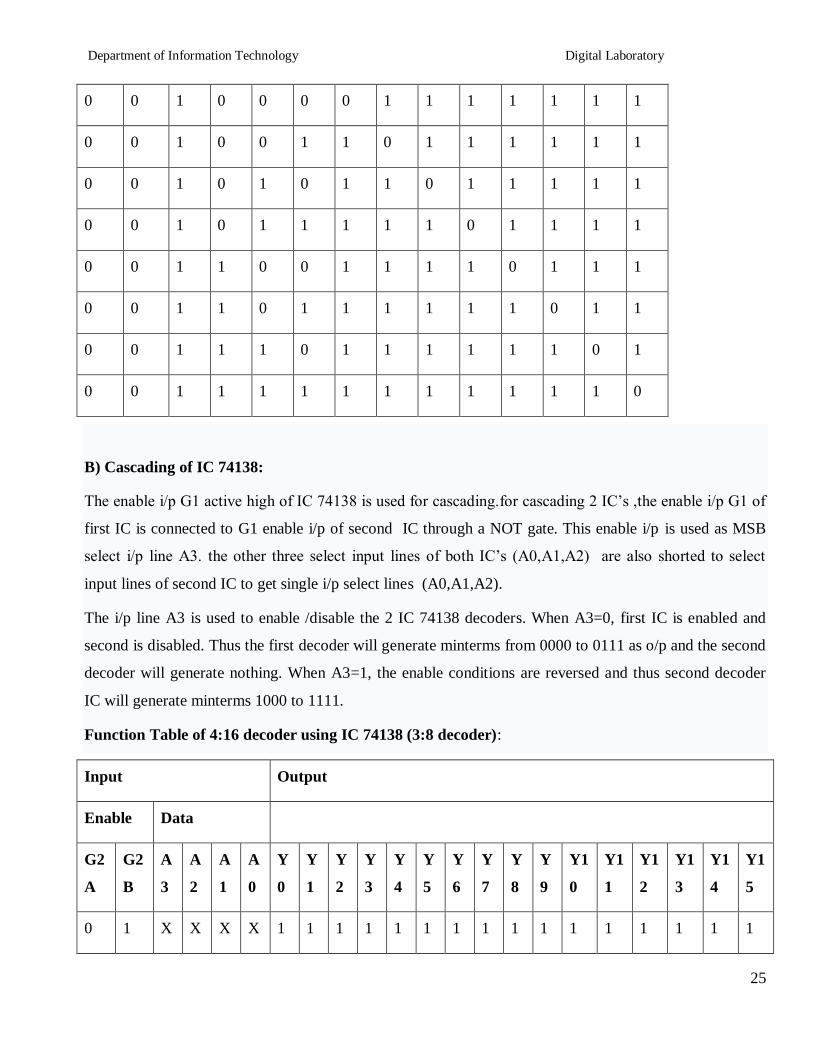
Department of Information Technology Digital Laboratory
29
pulse are counted to be made of it goes up step by step amp the op of counter in the flip flop is decoded to
read the count to its starting step after counting n pulse incase of module counters
Types of Counters
Counter are of two types
1) Asynchronous counter
2) Synchronous counter
Asynchronous counter
A digital counter is a set of flip flop The flip flop are connected such that their combined state at any time
is binary equivalent of total no of pulses that have occurred up to that time Thus its name implies a
counter is used to count pulse A counter is used as frequency dividers To obtain waveform with
frequency that is specific fraction of clock frequency
Counter may be Asynchronous or synchronous The Asynchronous counter is also called as ripple counter
An Asynchronous counter uses T flip flop to perform a counting function The actual hardware used is
usually J-K flip flop with J amp K connected to logic1Even D flip flops may be used here
In asynchronous counter commonly called ripple counter the first flip-flop is clocked by the external
clock pulse amp then each successive flip-flop is clocked by the Q or Qrsquo output of the previous flip-flop
Therefore in an asynchronous counter the flip-floprsquos are not clocked simultaneously The input of MS-JK
is connected to VCC because when both inputs are one output is toggled As MS-JK is negative edge
triggered at each high to low transition the next flip-flop is triggered
Synchronous Counter
When counter is clocked such that each flip flop in the counter is
triggered at the same time the counter is called as synchronous counter
The gates propagation delay at reset time will not be present or we may say will not occur
1) Asynchronous Up Counter
Fig 1 shows 3bit Asynchronous Up Counter Here Flip-flop 2 act as a MSB Flip-flop and Flip-flop 0 act
as a LSB Flip-flop Clock pulse is connected to the Clock of Flip-flop 0 Output of Flip-flop 0(Q0) is
connected to clock of next flip-flop (ie Flip-flop 1) and so on As soon as clock pulse changes output is
going to change (at the negative edge of clock pulse) as a Up count sequence For 3 bit Up counter state
table is as shown below
Department of Information Technology Digital Laboratory
30
State Table
Logic diagram
Fig 1 3 Bit Asynchronous Up Counter
Hardware requirements
Gate
Flip flop
Quantity IC Quantity
MS JK 3 7476 2
2) Down Counter
Fig 2 shows 2 bit Asynchronous Down Counter Here Flip-flop 2 act as a MSB Flip-flop and Flip-flop 0
act as a LSB Flip-flop Clock pulse is connected to the Clock of Flip-flop 0 Output of Flip-flop 0 (Q0rsquo) is
Counter States Count
Q2 Q1 Q0
0 0 0 0
1 0 0 1
2 0 1 0
3 0 1 1
4 1 0 0
5 1 0 1
6 1 1 0
7 1 1 1
8 0 0 0
Department of Information Technology Digital Laboratory
31
connected to clock of next flip-flop (ie Flip-flop 1) and so on As soon as clock pulse changes output is
going to change (at the negative edge of clock pulse) as a down count sequence For 3 bit down counter
sate table is as shown below
In both the counters Inputs J and K are connected to Vcc hence J-K Flip flop work in toggle mode Preset
and Clear both are connected to logic 1
State Table
Logic diagram
Fig 2 3 Bit Asynchronous Down Counter
Hardware requirements
Counter States Count
Q2 Q1 Q0
7 1 1 1
6 1 1 0
5 1 0 1
4 1 0 0
3 0 1 1
2 0 1 0
1 0 0 1
0 0 0 0
7 1 1 1
Department of Information Technology Digital Laboratory
32
Gate
Flip flop
Quantity IC Quantity
MS JK 3 7476 2
Applications
The asynchronous counters are specially used as the counting devices
They are also used to count number of pulses applied
It also works as frequency divider
It helps in counting the number of product coming out of the machinery where product is coming out at
equal interval of time
Types of synchronous counter
1) Up counter
2) Down counter
1 3 bit Synchronous up counter
The up counter counts from 0 to7 ie(000 to 111)for this we are using MS JK flip flop In IC 74LS76 2
MS J-K flip flops are present The clock pulse is given at pin 1 amp 6 of the 1st IC amp pin 1 of 2nd IC Next
state decoder logic is designed with the help of state table
State table for synchronous up counter
Present state Next state Flip flop 3 Flip flop 2 flip flop 1
Q2 Q1 Q0 Q2 Q2 Q0 J2 K2 J1 K1 J0 K0
0 0 0 0 0 1 0 x 0 X 1 x
0 0 1 0 1 0 0 x 1 X x 1
0 1 0 0 1 1 0 x x 0 1 x
0 1 1 1 0 0 1 x x 1 x 1
1 0 0 1 0 1 x 0 0 X 1 X
1 0 1 1 1 0 x 0 1 X x 1
1 1 0 1 1 1 x 0 x 0 1 X
1 1 1 0 0 0 x 1 x 1 x 1
Department of Information Technology Digital Laboratory
33
K-Map
Q1Q0
Q2
00 01 11 10
0 0 0 1 0
1 X X X X
J2= Q1Q0
Q1Q0
Q2
00 01 11 10
0 X X X X
1 0 0 1 0
K2= Q1Q0
Q1Q0
Q2
00 01 11 10
0 0 1 X X
1 0 1 X X
J1= Q0
Q1Q0
Q2
00 01 11 10
0 X X 1 0
1 X X 1 0
K1= Q0
Department of Information Technology Digital Laboratory
34
Q1Q0
Q2
00 01 11 10
0 1 X X 1
1 1 X X 1
J0= 1
Q1Q0
Q2
00 01 11 10
0 X 1 1 X
1 X 1 1 X
K0= 1
Logic Diagram
Fig 1 3 bit Synchronous up counter
Department of Information Technology Digital Laboratory
35
2 3 bit Synchronous down counter
This is used to count from 7-0 ie(111-000)for this also 2 ICrsquos of 74LS76 are required amp hence we use 3
MS JK flip flops Here also clock is given to 1stamp 6th pin of 1st IC amp1st pin of 2nd IC enabling to apply
clock to all flip flop at a time Next state decoder logic is designed with the help of state table
State table for synchronous down counter
Present state Next state Flip flop 3 Flip flop 2 Flip flop 1
Q2 Q1 Q0 Q2 Q1 Q0 J2 K2 J1 K1 J0 K0
1 1 1 1 1 0 X 0 X 0 X 1
1 1 0 1 0 1 X 0 X 1 1 X
1 0 1 1 0 0 X 0 0 X X 1
1 0 0 0 1 1 X 1 1 X 1 X
0 1 1 0 1 0 0 X X 0 X 1
0 1 0 0 0 1 0 X X 1 1 X
0 0 1 0 0 0 0 X 0 X X 1
0 0 0 1 1 1 1 X 1 X 1 X
K-Map
Q1Q0
Q2
00 01 11 10
0 1 0 0 0
1 X X X X
J2= Q1Q0
Q1Q0
Q2
00 01 11 10
Department of Information Technology Digital Laboratory
36
0 X X X X
1 1 0 0 0
K2= Q1Q0
Q1Q0
Q2
00 01 11 10
0 1 0 X X
1 1 0 X X
J1= Q0
Q1Q0
Q2
00 01 11 10
0 X X 0 1
1 X X 0 1
K1= Q0
Q1Q0
Q2
00 01 11 10
0 1 X X 1
1 1 X X 1
J0= 1
Q1Q0
Q2
00 01 11 10
0 X 1 1 X
1 X 1 1 X
K0= 1
Department of Information Technology Digital Laboratory
37
Logic Diagram
Fig 2 3 bit Synchronous down counter
Uses
1 Specially used as the counting devices
2 Used in frequency divider circuit
3 Used in digital voltmeter
4 Used in counter type A to D converter
5 Used for time measurement
6 It helps in counting the no of product coming out from machinery where product is coming out
at equal interval of time
Conclusion
Up and down counters are successfully implemented the counters are studied amp op are checked The
state table is verified
PRACTICE ASSIGNMENTS EXERCISE MODIFICATIONS
1 Design amp implement 2 bit controlled synchronous counter
2 Designamp implement 4 bit controlled synchronous counter
3 Designamp implement truncated synchronous up or down counter
FAQrsquos with answers
1 What do you mean by Counter
A Counter is a register capable of counting the no of clock pulses arriving at its
clock inputs Count represents the no of clock pulses arrived A specified
sequence of states appears as the counter output
Department of Information Technology Digital Laboratory
38
2 What are the types of Counters Explain each
There are two types of counters as Asynchronous Counter and Synchronous Counter
Asynchronous Counter In this counter the first flip-flop is clocked by the external clock pulse
and then each successive flip-flop is clocked by the Q or Qrsquo op of the previous flip-flop Hence in
Asynchronous Counter flip-flops are not clocked simultaneously and hence called as Ripple
Counter Synchronous Counter In this counter the common clock input is connected to all the
flip-flops simultaneously
3 What do you mean by pre-settable counters
A counter in which starting state is not zero can be designed by making use of the
preset inputs of the flip flops This is referred to as loading the counter
asynchronously This is referred to as pre-settable counter
4 What are the applications of synchronous counters
Digital clock
Frequency divider circuits
Frequency counters
Used in analog to digital converters
5 What are the advantages of synchronous counters over asynchronous counters
Propagation delay time is reduced
Can operate at a much higher frequency than the asynchronous counters
6 Ring counter is an example of synchronous counters or asynchronous counter
Synchronous counter Since all the flip flops are clocked simultaneously
7 Twisted Ring (Johnsonrsquos) counter is an example of synchronous counters or asynchronous
counter
Synchronous counter Since all the flip flops are clocked simultaneously
8 What is the difference between ring counter and twisted ring counter
In ring counter pulses to be counted are applied to a counter it goes from state to state and the
output of the flip flop s in the counter is decoded to read the count Here the uncomplimentary
output (Q) of last flip flop is fed back as an input to first flip flop Ring counters are referred as
MOD lsquoNrsquo counters
Department of Information Technology Digital Laboratory
39
But in Twisted ring counter the complimentary output (Q bar) of last flip flop is fed back as an
input to first flip flop Twisted Ring counters are referred as MOD lsquo2Nrsquo counters
9 What are the applications of ring counters
Ring counter outputs are sequential non-overlapping pulses which are useful for control state
counters Used in stepper motor this requires pulses to rotate it from one position to the next Used
as divide by lsquoNrsquo ((MOD lsquoNrsquo) counters
10 What are the applications of ring counter twisted ring counters
Used as divide by lsquo2Nrsquo ((MOD lsquo2Nrsquo) counters
Used for control state counters
Used for generation of multiphase clock
11 List the Synchronous Counter ICs
IC 74160 Decade Up Counter
IC 74161 4 bit binary Up Counter
IC 74162 Decade Up Counter
IC 74163 4 bit binary Up Counter
IC 74168 Decade UpDown Counter
IC 74169 4 bit Binary UpDown Counter
IC 74190 Decade UpDown Counter
IC 74191 4 bit Binary UpDown Counter
IC 74192 Decade UpDown Counter
IC 74193 4 bit Binary UpDown Counter
Department of Information Technology Digital Laboratory
40
Regularity Content Viva-voce Timely
Submission Total
Dated Sign of
Subject
Teacher
2 4 2 2 10
Date of Performance Date of Completion
-------------------------------------------------------------------------------------------------------------------
Assignment No 5
-------------------------------------------------------------------------------------------------------------------------------
Title Design and implementation of Module lsquonrsquo counter with IC7490 and IC 74191
-----------------------------------------------------------------------------------------------------------------------------
Objective To know difference between regular amp truncated counter as well as binary ampBCD Counter
--------------------------------------------------------------------------------------------------------------------------------
Problem Statement To design and implement mod - 10 mod ndash 7 mod - 99 asynchronous BCD
counter using IC 7490 and to design and implement up down mod - n Binary counter using IC 74191
-----------------------------------------------------------------------------------------------------------------
Hardware Requirement
i) IC 7490 IC 74191 basic gates
ii) Digital Trainer Kit -1
iii) Patch cords
----------------------------------------------------------------------------------------------------------------
Software Requirement Digital Work 30
------------------------------------------------------------------------------------------------------------------
Theory
Part A ndash IC 7490
IC 7490 is a TTL MSI (medium scale integration) decade counter It contains 4 master slave flip flops
internally connected to provide MOD-2 ie divide by 2 and MOD-5 ie divide by 5 counters MOD-2 and
Mod-5 counters can be used independently or in cascading
Department of Information Technology Digital Laboratory
41
It is a 4-bit ripple type decade counter The device consists of 4-master slave flip flops internally
connected to provide a divide by two and divide by 5 sections Each section has a separate clock ip to
initiate state changes of the counter on the high to low clock transition
Since the op from the divide by 2 section is not internally connected to the succeeding stages The device
may be operated in various counting modes In a BCD counter the CP1 input must be externally connected
to QA op The CP0ip receives the incoming count producing a BCD count sequence It is also provided
with additional gating to provide a divide by 2 counter and binary counter for which the count cycle length
is divide by 5 The device may be operated in various counting modes
There are 2 reset inputs R0(1) and R0(2) both of which need to be connected to the lsquologic 1rsquo for clearing all
flip flops Two set inputs Rg(1) and Rg(2) when connected to logic 1 are used for setting counter to 1001
(BCD 9)
Pin out of IC 7490
Fig Pin configuration of IC7490
Table 1-pin name and description of IC7490
Pin name Description
Input B This is clock input to the internal MOD-5 ripple counter which is negative
edge triggered
R0(1)R0(2) Gated zero reset inputs
Department of Information Technology Digital Laboratory
42
R9(1)R9(2) These are gated set to nine inputs
QDQCQB Output of internal MOD-5 counter with QD as MSB
QA Output of internal MOD-2 counter with QA as LSB
Input A Clock input to FF-A which is negative edge triggered
Functional Table for IC7490
Reset inputs Output
R0(1) R0(2) R9(0) R9(1) QD QC QB QA
1 1 0 X 0 0 0 0
1 1 X 0 0 0 0 0
X X 1 1 1 0 0 1
X 0 X 0 COUNTER
0 X 0 X COUNTER
0 X X 0 COUNTER
X 0 0 x COUNTER
Department of Information Technology Digital Laboratory
43
Basic internal Structure of IC 7490
Function Table of MOD-5 counter
Design of MOD-10 counter using IC 7490
The QA op the first flip flop is connected to the input B which is clock ip of internal MOD-5 ripple
counter Due to cascading of Mod-2 and Mod-5 counters the overall configuration the decade counters
count from 0000 to 1001 After 1001 mod-5 resets to 0000 and next count after 1001 is 0000
When QA op is connected to B ip we have the Mod-2 counter followed by Mod-5 counter The
count sequence obtained is shown in the table It may be noted that QA changes from 0 to 1 the state of
InputB clock Output
Count QD QC QB
0 0 0 0
0 0 1 1
0 1 0 2
0 1 1 3
1 0 0 4
Department of Information Technology Digital Laboratory
44
Mod-5 counter doesnrsquot change whereas when QA changes from 1 to 0 the Mod-5 counter goes to the next
state
Logic DiagramMOD-10 counter using IC 7490
5 Modulus n Counter
Function table
Ip clock
Output
Count QD QC QB QA
0 0 0 0 0
0 0 0 1 1
0 0 1 0 2
0 0 1 1 3
0 1 0 0 4
Department of Information Technology Digital Laboratory
45
Design of Mod-7 Counter using IC 7490
Mod-7 counter counts through seven states from 0 to 6 counters and it should reset as soon as the
count becomes 7 The op of reset logic should be 1 corresponding to invalid states The reset logic op
should be applied to pin 2 and 3
Truth Table of Reset Logic
0 1 0 1 5
0 1 1 0 6
0 1 1 1 7
1 0 0 0 8
1 0 0 1 9
QD QC QB QA Y
0 0 0 0 0
0 0 0 1 0
0 0 1 0 0
0 0 1 1 0
0 1 0 0 0
0 1 0 1 0
0 1 1 0 0
0 1 1 1 1
1 0 0 0 1
1 0 0 1 1
Department of Information Technology Digital Laboratory
46
Logic Diagram Mod 7 Counter using IC 7490
Function table
Ip clock
Output
Count QD QC QB QA
0 0 0 0 0
0 0 0 1 1
0 0 1 0 2
0 0 1 1 3
0 1 0 0 4
0 1 0 1 5
0 1 1 0 6
Department of Information Technology Digital Laboratory
47
Design of Mod-99 using IC 7490
For Mod-99 two IC 7490rsquos will be required Hence to implement a divide by 99 counter we have
to use two decade counters ICrsquos A divide by 99 counter counts 99 states from 0 to 98 and the counter
should reset as soon as the count becomes 99 So in order to reset the counter of 99 connect the Q op
which are equal to 1 in the count of 99 to an lsquoAndrsquo gate amp then connect and op to the reset ip of both
ICrsquos
MOD-100 Counter-
MOD-100 counter can be obtained by cascading two decade counter ICrsquos
Each IC gives divide by 10 counts Hence 2 ICs will give 1010=100 counts
Clock is applied to the input A of IC 7490 the Q1 output is connected to B input etc
For cascading the QD output of the first IC is connected to the input A of second IC Thus QD of
IC-(1) acts as clock input to IC-(2)
The Ro (1) Ro(2) R9(1) R9(2) inputs of both ICs are connected to ground so as to make them
inactive
The total count provided by the two counters varies from 00 to 99 decimal that means 100 states
Hence it is a MOD-10 counter
Impleacutementations
FigureMOD-100 counters using IC 7490
Department of Information Technology Digital Laboratory
48
B) IC 74191 ndash Theory
IC74191 is 4-bit binary synchronous reversible up down counter It contains 4 master slave flip flops
with internal gating and steering logic to provide asynchronous reset and synchronous count updown
operations its asynchronous parallel capability permits the counter to be preset to any desire number D0
to D3 are the parallel data inputs Information present on the parallel data inputs D0 to D3 is loaded into
the counter and appears on the output when the load PLinput is lowThisoperation overrides the counting
function Counting is inhabited by the high level on the enable G input when G input is low internal state
changes are initiated synchronously by the low to high transitions of the clock inputs the updown input
signal determines the direction of input
Function Table
Operating
mode
Inputs Outputs
PL UD G CLK Dn
Parallel
load L X X X L L
L X X X H H
Count up H L 0 uarr X Count up
Count
down H H 0 uarr X
Count
down
Hold(No
change) H X H X X No change
Pin details ndash
D0 to D3 input lines PL parallel load
G is Enable input ndash enabling the counting
Q0 to Q3 output lines
Downup determines the direction of counting
Clk clock input for counter
Terminal Count Max(1111) min(0000) For these states signal goes high for 1clock pulse
Ripple clock Clock input for next higher state
Department of Information Technology Digital Laboratory
49
Pin Diagram IC 74191
Up counter- Truth Table
Clk
Pulses QA QB QC QD
0 0 0 0 0
1 0 0 0 1
2 0 0 1 0
3 0 0 1 1
4 0 1 0 0
5 0 1 0 1
6 0 1 1 0
7 1 1 1 1
8 1 0 0 0
9 1 0 0 1
10 1 0 1 0
11 1 0 1 1
12 1 1 0 0
13 1 1 0 1
Department of Information Technology Digital Laboratory
50
14 1 1 1 0
15 1 1 1 1
Logic Diagram
Steps-
Connect the circuit as shown above
Apply clock ip to pin no14
Connect UD to GND
Verify the output according to truth table
Logic diagram of down counter
Steps-
Connect the circuit as shown above
Apply clock ip to pin no14
Connect UD to VCC
Verify the output according to truth table
UD D3 D2 D1 D0 PL
Clock IC 74191
G RC
MAX MIN
Q3 Q2 Q1 Q0 TC
vcc
NC
NC
Outputs
no connection
vcc
Department of Information Technology Digital Laboratory
51
With the help of IC74191 we can implement truncated updown counter by using following logic ndash
Connect data input line to particular count you want to load
According to requirement make Truth table
Draw the K-map
Find out Boolean expression
Draw the logic diagram and that is the combinational logic for your count and apply the output of
that circuit to PL
According to requirement we get the UP and down counting
5 Modulus n Counter
Presettable updown counter
Mod 11 counter
Implementation of presetttable mod updown counter using IC- 74LS191
1 Load Data on data lines D0 to D3 (0101)
2 Counter will go through the states from 0101 0110hellip1111 in up counter and 0101 to 0000 in
down counter
Combinational Circuit
CLOCK D3 D2 D1 D0
TC
U D 74191 RC
G PL
Updown Q3 Q2 Q1 Q0 PL
Q3 Q2 Q1 Q0
Preset Count
Department of Information Technology Digital Laboratory
52
3 The logic circuit should be designed in such a way that only when all the outputs are high output
of the reset circuit should be low and the counter should jump to state 5 It should again start
counting from 0101 to 0000
State Table
Down Counter UP Counter
IC 74191 is 4 bit counter Thus it counts 0000 to 1111 different 16 states For MOD11 counter we require
different 11 states so 5 steps must be skipped from 16 states We get MOD11 by presetting counter to
value 5
Assignment Question
Design and Implement MOD 7 MOD 10 and MOD 12 using IC 74191
FAQs
1 What do you mean modulus counter
Counter
state Clock
pulse
Q3 Q2 Q1 Q0
1 0 1 0 1
2 0 1 1 0
3 0 1 1 1
4 1 0 0 0
5 1 0 0 1
6 1 0 1 0
7 1 0 1 1
8 1 1 0 0
9 1 1 0 1
10 1 1 1 1
11 1 1 1 1
Counter state
Clock pulse
FF outputs
Q3 Q2 Q1 Q0
1 0 1 0 1
2 0 1 0 0
3 0 0 1 1
4 0 0 1 0
5 0 0 0 1
6 0 0 0 0
7 0 1 0 1
Department of Information Technology Digital Laboratory
53
It represents the number of possible states of counter
2 How will you use the 7490 IC to design symmetrical divide by 10 frequency counter
The divide by 5 circuit followed by divide by 2 circuit will give symmetrical output
3Where counters are used Give real life example of counter
Modulus n Counter
Binary counter ndash An N stage counter that recycles after 2 Ncount The count proceds in specified binary
sequence Counter Presetable- A counter which can be set to a desired value before the start of the
counting UPDown counter ndash A counter that can count in both up and down direction depending upon a
control input
Department of Information Technology Digital Laboratory
54
Regularity Content Viva-voce Timely
Submission Total
Dated Sign of
Subject
Teacher
2 4 2 2 10
Date of Performance Date of Completion
-------------------------------------------------------------------------------------------------------------------
Assignment No6
------------------------------------------------------------------------------------------------------------------
Title Sequence Generator
------------------------------------------------------------------------------------------------------------------
Objective To understand sequence generator one of the sequential circuit
-------------------------------------------------------------------------------------------------------------------
Problem Statement Design (State Diagram State Table K Map) and implementation of Sequence
Generator using Shift Register IC 74194
-----------------------------------------------------------------------------------------------------------------
Hardware Requirement
i) IC 741947408 (AND-gate) 7432 (OR-gate)
ii) Digital Trainer Kit -1
iii) Patch cords
----------------------------------------------------------------------------------------------------------------
Software Requirement Digital Work 30
------------------------------------------------------------------------------------------------------------------
Theory
Part A Sequence Generator with Flip flop
A sequential circuit which generates a prescribed sequence of bits in synchronism with a clock is referred
to as a sequence generator These pulse trains or sequence of bits can be used to open valves close gates
turn on lights and turn off machines and other variety of jobs
Department of Information Technology Digital Laboratory
55
For the design of sequence generator we first determine the required no of flip flops and the logic circuit
for the next state decoder
No of flip flops required to generate particular sequence can be determined as follows
1) Find the no of 1rsquos in the sequence
2) Find the no of 0rsquos in the sequence
3) Take the maximum out of two
4) If N is the required no of flip flops choose minimum value of lsquonrsquo to satisfy equation given below
Max (0rsquos 1rsquos) le 2n-1
The sequence generator can be classified as
1) sequence generator without bushing
2) sequence generator with bushing
The aim in this experiment is to design a sequence generator to generate a sequence of bit ie 10101
Part B Sequence Generator using Shift Register IC 74194
IC 74194 4 bit bidirectional Shift Register
This bidirectional shift register is designed to incorporate virtually all the features a system designer may
want in a shift register they feature Parallel inputs parallel outputs right shift left shift serialinputs
operating mode control inputsand a direct overriding clear line The register has four distinct modes of
operationsnamely
1 Parallel load
2 Shift right (in the direction QA towards QD)
3 Shift left (in the direction QD towards QA)
4 Inhibit clock (do nothing)
Synchronous parallel loading is accomplished by applying the four bits of data and taking both
mode control inputs S0 and S1High The data is loaded in to the associated flip-flops and appear
at the outputs after positive transition of the clock input During loading serial data flow is
inhibited
Shift right is accomplished synchronously with the rising edge of the clock pulse when S0 is High
and S1 is Low Serial data for this mode is entered at the shift right data input When S0 is Low
and S1 is High data shifts left synchronously and new data is entered at the shift left serial input
Clocking of the flip flop is inhibited when both mode control inputs are LOW
Department of Information Technology Digital Laboratory
56
Mode Control Input Operation
S1 S0
0 0 Clock Inhibit
0 1 Shift right
1 0 Shift Left
1 1 Parallel loading
Function Table of IC 74194
Design
The minimum number of flip-flops N required to generate a sequence of length S is given by S
le 2N ndash 1
In this case S=7 therefore the minimum value of N which may generate in this sequence is 3
However it is not guaranteed to lead to a solution If the given sequence leads to seven distinct
states then only three flip flops are sufficient otherwise we have to increase the number of flip
flops We write the states of circuit as given in table 1 The prescribed sequence is listed under QA
and the sequence listed under QB and QC are the same sequence delayed by one and two clock
pulses respectively From the table we observe that all the states are not distinct which means N=3
is not sufficient Next we assume that N=4 and prepare table 2 The last column gives the required
serial input for getting the desired change of state when a clock pulse is applied This is obtained
by assuming D type flip flop and looking at the QA output For example at the falling edge of first
clock pulse QA=1 The second clock pulse must result in QA=1 which requires its D input to be 1
In the same manner all the entries in column Y are determined
Table 1 State Assignment Table of Sequence Generator (N=3)
Number of Clock
Pulses
Flip Flop Inputs States
QA QB QC
1 1 1 1 7
2 1 1 1 7
3 0 1 1 3
4 1 0 1 5
Department of Information Technology Digital Laboratory
57
5 0 1 0 2
6 1 0 1 5
7 1 1 0 6
Excitation table of D Flip-Flop
Present State Qn Next State Qn+1 Flip-Flop Input D
0 0 0
0 1 1
1 0 0
1 1 1
Table 2State Assignment Table of Sequence Generator (N=4)
Number of Clock
Pulses
Flip Flop Inputs States
Y
Serial ip QA QB QC QD
1 1 1 1 0 14 1
2 1 1 1 1 15 0
3 0 1 1 1 7 1
4 1 0 1 1 11 0
5 0 1 0 1 5 1
6 1 0 1 0 10 1
7 1 1 0 1 13 1
K-Map Simplification
Department of Information Technology Digital Laboratory
58
00 01 11 10
00 X X X X
01 X 1 1 X
11 X 1 0 1
10 X X 0 1
Y= QArsquo + QBrsquo + QCrsquo = QAQBQC
LOGIC DIAGRAM
HARDWARE REQUIREMENTS
Sr no ICs Description Quantity
11 74194 4 bit bidirectional universal shift register 16ktr`
2 7410 3 input NAND Gate 1
Department of Information Technology Digital Laboratory
59
Conclusion In this way sequence generator using JK flip flips amp shift register is designed and
implemented
Enhancements Modifications ndash Sequence generator can also be implemented with shift register instead
of flip flops Use IC 7495 universal shift register IC and try to implement sequence generator
FAQs
1 What is sequential logic circuit
A sequential logic circuit consists of a memory elements in addition to
combinational circuit Its output at any instant of time depends upon
the present input as well as present state of memory element
2 What is meant by delay line
It is used to introduce time delays in digital signals
3 What is meant by following terms
a) Synchronous preset b) Asynchronous preset
c) Synchronous clear d) Asynchronous clear
a)Preset operation is synchronised with the clock
b)Preset operation is independent of the clock
c) clear is performed in synchronous with clock
d) clear is performed independent with clock
4 Is asynchronous counter faster than synchronous counter
In a synchronous counter the time required for change of any state is same and is equal to delay
time of one flip flop where as in asynchronous counter all flip flops are not clocked
simultaneously hence time required is not same
5 What is mean by lockout in counter
In a counter design for a fewer state than the maximum possible state some time it may so happen
that counter enters in unused state and goes from one unused state to another unused state and
never comes to used state
6 What is mean by state table
Department of Information Technology Digital Laboratory
60
It consists of complete information about present state and next state and outputs of a sequential
system
7 What is mean by state diagram
The information available in a state table can be represented as graphically the graphical
representation is known as state diagram
8 What is the advantage of state reduction in the design of sequential circuit
It reduces the number of flip flops
9 What is meant by excitation table
This gives information about what should be the flip flop inputs if outputs are specified before and
after the clock pulse
10 How many flip flops are required to design sequence generator using Counters
max (0rsquoS1rsquoS) in a given sequence lt= 2(N - 1)
Where N = Number of flip flops
11 How many flip flops are required to design sequence generator using shift registers
Slt= 2N - 1
Where N=Number of flip flops
S= Length of sequence
12 What is Lock out condition How it is avoided
When counter enters into one of the invalid state and after application of pulses remains in invalid
states only i e counter gets locked into invalid state amp this is called as lock out Lock out can be
avoided by providing bushing to all the invalid states in such a way that after application of one or
more clock pulses counter will fall into one of the valid state
Department of Information Technology Digital Laboratory
61
Regularity Content Viva-voce Timely
Submission Total
Dated Sign of
Subject
Teacher
2 4 2 2 10
Date of Performance Date of Completion
-------------------------------------------------------------------------------------------------------------------
Assignment No7
------------------------------------------------------------------------------------------------------------------
Title Multiplexer using Data flow modeling and structural modeling
------------------------------------------------------------------------------------------------------------------
Objective To learn data flow modeling style Its uses and different types of declarations with some
different types of circuits Structure of VHDL program is well discussed with this modeling style
-------------------------------------------------------------------------------------------------------------------
Problem Statement 41 multiplexer using data flow amp structural modeling -
----------------------------------------------------------------------------------------------------------------
Hardware Requirement - NA
----------------------------------------------------------------------------------------------------------------
Software Requirement Xilinx
------------------------------------------------------------------------------------------------------------------
Theory
Data flow style-
In this type of design the view of data as flowing from input to output through a design
An operation is defined in terms of a collection of data transformation expressed as concurrent
statement Each of the statement can be activated when any of its input signal changes its value While
these statements describe the behavior of the circuit a lot of information about its structure can be
extracted from the description as well
Data flow modeling has a set of concurrent assignment statements In the data flow level of abstraction we
describe how information is passed in the circuit The built in operators in VHDL are used in expression
such as AND OR XOR NOT etc
Department of Information Technology Digital Laboratory
62
INPUT
Two select lines S1S0
Four data lines D0 D1 D2 D3
OUTPUT
One output line Y
Functional block diagram of 41 Mux
Fig 41 Multiplexer using Data flow modeling
Function table of 41 Mux
Enable S1 S0 A B C D Y
1 X X X X X X 0
0 0 0 A X X X A
0 0 1 X B X X B
0 1 0 X X C X C
0 1 1 X X X D D
Design steps
Click on Xilinx ISE 92i
Create New project from file menu Ensure top level source is HDL
Select family of devices (usually spartan2E or 3)
Department of Information Technology Digital Laboratory
63
Ensure preferred language is VHDL
Click new source which shows you project details device details
and Synthesis and simulator tools
After finishing project create new source by right clicking in project name with VHDL
module
Complete ports name directions and bus Ensure architecture name is behavioral
After that we will get design summary and detailed reports
Close design summary
Create your code with given modeling style
Go to process window and synthesis to check if any error is there in code Check syntax and
view RTL schematic
Create new source to simulate the code
Right click on source name and create test bench waveform with proper name Ensure the
project is same
Click on combinational circuit in initial timing wizard
Select test bench wave in source window Apply inputs to wave diagram Ensure you are in
behavioral simulation
Go to process box Click on Xilinx ISE simulator and simulate the model See results
RTL Schematic
Department of Information Technology Digital Laboratory
64
Timing Diagram
FAQrsquos
1 What are the different kinds of data objects in VHDL code
Ans data object may be any value or number still some signal data objects and bit and bit_vector
types of these are available in VHDL STD_LOGIC and STD_LOGIC_VECTOR types are used
widely in programming
2 What do you mean by signal
Ans signal is a data object represents logic signals or wires in a circuit There are three places in
which signals can be declared in VHDL code in an entity declaration in the declarative section of
architecture and in declarative section of package
3 What are different signal types
Ans BIT BIT_VECTOR STD_LOGIC STD_LOGIC_VECTOR STD_ULOGIC SIGNED
UNSIGNED INTEGER ENUMERATION and BOOLEAN
4 What is an entity
Ans a circuit or sub circuit described with VHDL code is called a design entity
5 Explain structure of an entity
Ans it has two main parts the entity declaration which specifies the input and output signals for
entity and the architecture which gives circuit details
Department of Information Technology Digital Laboratory
65
6 How will you declare a package with component Explain structure
The general form of package declaration is as shown in diagram
PACKAGE package_name IS
[TYPE declarations]
[SIGNAL declarations]
[COMPONENT declarations]
END package_name
Entity
Declaration Architecture
Department of Information Technology Digital Laboratory
66
Regularity Content Viva-voce Timely
Submission Total
Dated Sign of
Subject
Teacher
2 4 2 2 10
Date of Performance Date of Completion
-------------------------------------------------------------------------------------------------------------------
Assignment No8
------------------------------------------------------------------------------------------------------------------
Title Full Adder using Behavioral and Structural modeling
------------------------------------------------------------------------------------------------------------------
Objective To learn structural modeling style Its uses and different types of declarations with some
different types of circuits Structure of VHDL program is well discussed with this modeling style
-------------------------------------------------------------------------------------------------------------------
Problem Statement Full adder using behavioral amp structural modeling
-----------------------------------------------------------------------------------------------------------------
Hardware Requirement - NA
----------------------------------------------------------------------------------------------------------------
Software Requirement Xilinx
------------------------------------------------------------------------------------------------------------------
Theory
Structural style-
A digital electronic system can be described as a module with inputs andor outputs The electrical values
on the outputs are same functions of the values of inputs The example of it is as shown The NAND gate
has 2ips AampB amp an output y Using VHDL terminology we call the NAND2 design entity amp the inputs
amp outputs are called ports 1 way of describing the function of NAND2 is to describe how it is composed
of sub modules AND amp INVERTER Each of the Sub modules is an instance of some entity amp ports of the
instances are connected using signals Structural modeling has a set of interconnected component
Structure can be used to create a very low level description of a circuit or a very high level description
Department of Information Technology Digital Laboratory
67
In a gate level description of a circuit for example components such as basic logic gates amp FFs might be
connected in some logical stricture to create the circuit This is what is often called a net list
Structure of structural modeling
Functional block diagram of Full Adder
architectureNetlistofHalf_Adderis
-- component with locals
componentMyXorport (A_XorB_Xor in BIT
Z_Xor out BIT)
end component
-- component with locals
componentMyAndport (A_AndB_And in BIT
Z_And out BIT)
end component
begin
Xor1 MyXorport map (X Y Sum)
-- instance with actuals
And1 MyAndport map (X Y Cout)
-- instance with actuals
end
Department of Information Technology Digital Laboratory
68
Function table of Full Adder
A B Cin SUM CARRY
0 0 0 0 0
0 0 1 1 0
0 1 0 1 0
0 1 1 0 1
1 0 0 1 0
1 0 1 0 1
1 1 0 0 1
1 1 1 1 1
Sum = Σm(1 2 4 7)
Carry= Σm(3 5 6 7)
Design steps
Click on Xilinx ISE 92i
Create New project from file menu Ensure top level source is HDL
Select family of devices (usually spartan2E or 3)
Ensure preferred language is VHDL
Click new source which shows you project details device details
and Synthesis and simulator tools
After finishing project create new source(full adder) by right clicking in project name with
VHDL module
Complete ports name directions and bus Ensure architecture name is behavioral
After that we will get design summary and detailed reports
Close design summary
Click new source which shows you project details device details
and Synthesis and simulator tools
After finishing project create new source(half adder) by right clicking in project name with
VHDL module
Complete ports name directions and bus Ensure architecture name is behavioral Names
should be same as previous inputs
Department of Information Technology Digital Laboratory
69
After that we will get design summary and detailed reports
Close design summary
Create your code for half adder with given modeling style
After that go to process window Click on design utilities
View HDL instantiation code of half adder
Copy component part of half adder in architecture block of full adder Copy instantiation
template twice after begin as we require two half adders to construct full adder (structural
modeling) Name them differently (eg ha1 or ha2)
Create signals as per the logic Complete code of full adder
Go to process window and synthesis to check if any error is there in code Check syntax and
view RTL schematic
Create new source to simulate the code
Right click on source name and create test bench waveform with proper name Ensure the
project is same
Click on combinational circuit in initial timing wizard
Select test bench wave in source window Apply inputs to wave diagram Ensure you are in
behavioral simulation
Go to process box Click on Xilinx ISE simulator and simulate the model See results
RTL Schematic
Timing Diagram
Department of Information Technology Digital Laboratory
70
INPUT
Three inputs A B Carry (previous)
OUTPUT
Two outputs Sum Carry
FAQrsquos
1 What do you mean by structural style
Ans in this type of code a circuit is described in hierarchical fashion by connecting together sub
circuits
2 Explain IF statement with example
Ans The general form of an IF statement is as follws
IF Sel=rsquo0rsquo THEN
Flt=x1
ELSE
Flt=x2
END IF
Department of Information Technology Digital Laboratory
71
3 Explain declaration and instantiation process in VHDL
Ans first declare a small vhdl code in formal way Eg half adder Define project name is full adder
And simply copy instantiation template in main source code Define how many times you want to
declare this template Give separate names for those
4 What is STD_LOGIC_VECTOR
Ans It is standard data object added to VHDL standard in IEEE 1164 It provides more flexibility
than the Bit type
5 Explain difference between concurrent and sequential statements
Ans Concurrent statements define interconnected processes and blocks that together describe a designrsquos
overall behavior or structure They can be grouped using block sstatement Groups of blocks can also be
partitioned into other blocks At this same level a VHDL component can be connected to define signals
within the blocks
It is a reference to an entity A process can be a single signal assignment statement or a series of
sequential statements (SS) Within a process procedures and functions can partition the sequential
statements
PRACTICE ASSIGNMENTS
1 Implement half adder using data flow modeling
2 Implement Full Adder using behavioral modeling
3 Implement 3 bit magnitude comparator using a 3 bit adder
4 Implement half sub tractor using data flow modeling
5 Write VHDL code for Full Subtractor
Department of Information Technology Digital Laboratory
72
Regularity Content Viva-voce Timely
Submission Total
Dated Sign of
Subject
Teacher
2 4 2 2 10
rsquozaDate of Performance Date of Completion
-------------------------------------------------------------------------------------------------------------------
Assignment No9
------------------------------------------------------------------------------------------------------------------
Title Simulation of 3 bit Connter using Behavioral modeling
------------------------------------------------------------------------------------------------------------------
Objective To learn behavioral modeling style Its uses and different types of declarations with some
different types of circuits Structure of VHDL program is well discussed with this modeling style
-------------------------------------------------------------------------------------------------------------------
Problem Statement 3 bit controlled up down synchronous counter with preset amp clear
-----------------------------------------------------------------------------------------------------------------
Hardware Requirement -NA
----------------------------------------------------------------------------------------------------------------
Software Requirement Xilinx
------------------------------------------------------------------------------------------------------------------
Theory
Behavioral style-
Highest level of abstraction supported in VHDL is called the behavior level of abstraction In it we have
for loop while loop If then else case ampvariable assignment The statements are enclosed in a PROCESS
block amp are executed sequentially
In it circuit is described in terms of its operation overtime
In behavioral description the concept of time may be expressed precisely with actual delays between
related events (such as the propagation delays within gates amp on wires) or it may be simply an ordering of
operation that are expressed sequentially (such as in a functional description of a FF)
Department of Information Technology Digital Laboratory
73
A behavioral design method defines a circuit in terms of text language rather than a schematic of
interconnected symbols
Behavioral design is a technology independent text based design that incorporates high level
functionality amp high level information flow
Structure of Behavioral modeling
Functional block diagram of 3 bit controlled up down synchronous counter with preset amp clear
Function table of 3 bit controlled up down synchronous counter with preset amp clear
Design steps
Click on Xilinx ISE 92i
Create New project from file menu Ensure top level source is HDL
Select family of devices (usually spartan2E or 3)
Ensure preferred language is VHDL
Click new source which shows you project details device details
and Synthesis and simulator tools
After finishing project create new source by right clicking in project name with VHDL
module
Complete ports name directions and bus Ensure architecture name is behavioral
After that we will get design summary and detailed reports
Close design summary
Create your code with given modeling style
Go to process window and synthesis to check if any error is there in code Check syntax
and view RTL schematic Create new source to simulate the code
Department of Information Technology Digital Laboratory
74
Right click on source name and create test bench waveform with proper name Ensure the
project is same
Click on combinational circuit in initial timing wizard
Select test bench wave in source window Apply inputs to wave diagram Ensure you are in
behavioral simulation
Go to process box Click on Xilinx ISE simulator and simulate the model
RTL Schematic
Timing Diagram
INPUT
Clock Preset Clear
OUTPUT
Three output lines
FAQrsquos
1 Explain the structure of behavioral modeling
2 What are the differences between behavioral and structural modeling
Ans Behavioral descriptionof a circuit is the highest level of abstraction in VHDL Here the
circuit is described in terms of it operation with respect to time All operations are in one level of
code The operations are described in a way that the designer of a sequential circuit infers a
register
Structural description on the other hand is a circuit description in terms of its components
it can either create a low level description much like a hierarchy in a block diagram Whenever
you see a component instantiated in a code that code employs structural description of the circuit
The components are connected in the form of a netlist This is for better manageability and
reusability
3 What are the differences between behavioral and data flow modeling
Department of Information Technology Digital Laboratory
75
Ans Behavioral ndash describes how the output is derived from the inputs using structured
statements
Dataflow ndash describes how the data flows from the inputs to the output most often
using NOT AND and OR operations
4 What do you mean by process statement
Ans The process statement begins with the PROCESS keyword followed by a parenthesized list
of signals called the sensitivity list It operates on selected and conditional statements
5 Explain syntax of process statement
Ans BEGIN
Process( sensitivity list)
END process
PRACTICE ASSIGNMENTS
1 Implement 3 bit asynchronous up counter using behavioral modeling
2 Implement 3 bit asynchronous down counter using behavioral modeling
3 Implement 3 bit synchronous down counter using behavioral modeling
End
Department of Information Technology Digital Laboratory
76
Pin Diagrams
7400 Quad 2-Input NAND Gate
7402 Quad 2-Input NOR Gate
7404 Not Gates
7408 Quad 2-Input AND Gates
7432 Quad 2-Input OR Gate
7486 Quad 2-Input Exclusive-OR Gate
Department of Information Technology Digital Laboratory
77
7483 4 bit Binary Adder
7490 Decade and Binary Counters
74138 38 Decoder
Department of Information Technology Digital Laboratory
78
74153 Dual 41 Multiplexer
74191 Synchronous UpDown 4 bit Binary counter with Mode Control
Department of Information Technology Digital Laboratory
79
74194 Universal Shift Register
7476 Dual Master-Slave J-K Flip-Flops
- Part B Sequence Generator using Shift Register IC 74194
-
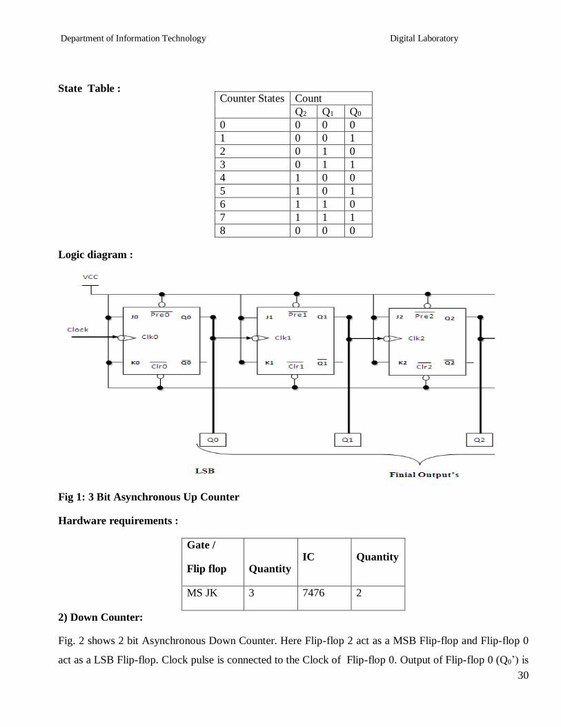
Department of Information Technology Digital Laboratory
32
Gate
Flip flop
Quantity IC Quantity
MS JK 3 7476 2
Applications
The asynchronous counters are specially used as the counting devices
They are also used to count number of pulses applied
It also works as frequency divider
It helps in counting the number of product coming out of the machinery where product is coming out at
equal interval of time
Types of synchronous counter
1) Up counter
2) Down counter
1 3 bit Synchronous up counter
The up counter counts from 0 to7 ie(000 to 111)for this we are using MS JK flip flop In IC 74LS76 2
MS J-K flip flops are present The clock pulse is given at pin 1 amp 6 of the 1st IC amp pin 1 of 2nd IC Next
state decoder logic is designed with the help of state table
State table for synchronous up counter
Present state Next state Flip flop 3 Flip flop 2 flip flop 1
Q2 Q1 Q0 Q2 Q2 Q0 J2 K2 J1 K1 J0 K0
0 0 0 0 0 1 0 x 0 X 1 x
0 0 1 0 1 0 0 x 1 X x 1
0 1 0 0 1 1 0 x x 0 1 x
0 1 1 1 0 0 1 x x 1 x 1
1 0 0 1 0 1 x 0 0 X 1 X
1 0 1 1 1 0 x 0 1 X x 1
1 1 0 1 1 1 x 0 x 0 1 X
1 1 1 0 0 0 x 1 x 1 x 1
Department of Information Technology Digital Laboratory
33
K-Map
Q1Q0
Q2
00 01 11 10
0 0 0 1 0
1 X X X X
J2= Q1Q0
Q1Q0
Q2
00 01 11 10
0 X X X X
1 0 0 1 0
K2= Q1Q0
Q1Q0
Q2
00 01 11 10
0 0 1 X X
1 0 1 X X
J1= Q0
Q1Q0
Q2
00 01 11 10
0 X X 1 0
1 X X 1 0
K1= Q0
Department of Information Technology Digital Laboratory
34
Q1Q0
Q2
00 01 11 10
0 1 X X 1
1 1 X X 1
J0= 1
Q1Q0
Q2
00 01 11 10
0 X 1 1 X
1 X 1 1 X
K0= 1
Logic Diagram
Fig 1 3 bit Synchronous up counter
Department of Information Technology Digital Laboratory
35
2 3 bit Synchronous down counter
This is used to count from 7-0 ie(111-000)for this also 2 ICrsquos of 74LS76 are required amp hence we use 3
MS JK flip flops Here also clock is given to 1stamp 6th pin of 1st IC amp1st pin of 2nd IC enabling to apply
clock to all flip flop at a time Next state decoder logic is designed with the help of state table
State table for synchronous down counter
Present state Next state Flip flop 3 Flip flop 2 Flip flop 1
Q2 Q1 Q0 Q2 Q1 Q0 J2 K2 J1 K1 J0 K0
1 1 1 1 1 0 X 0 X 0 X 1
1 1 0 1 0 1 X 0 X 1 1 X
1 0 1 1 0 0 X 0 0 X X 1
1 0 0 0 1 1 X 1 1 X 1 X
0 1 1 0 1 0 0 X X 0 X 1
0 1 0 0 0 1 0 X X 1 1 X
0 0 1 0 0 0 0 X 0 X X 1
0 0 0 1 1 1 1 X 1 X 1 X
K-Map
Q1Q0
Q2
00 01 11 10
0 1 0 0 0
1 X X X X
J2= Q1Q0
Q1Q0
Q2
00 01 11 10
Department of Information Technology Digital Laboratory
36
0 X X X X
1 1 0 0 0
K2= Q1Q0
Q1Q0
Q2
00 01 11 10
0 1 0 X X
1 1 0 X X
J1= Q0
Q1Q0
Q2
00 01 11 10
0 X X 0 1
1 X X 0 1
K1= Q0
Q1Q0
Q2
00 01 11 10
0 1 X X 1
1 1 X X 1
J0= 1
Q1Q0
Q2
00 01 11 10
0 X 1 1 X
1 X 1 1 X
K0= 1
Department of Information Technology Digital Laboratory
37
Logic Diagram
Fig 2 3 bit Synchronous down counter
Uses
1 Specially used as the counting devices
2 Used in frequency divider circuit
3 Used in digital voltmeter
4 Used in counter type A to D converter
5 Used for time measurement
6 It helps in counting the no of product coming out from machinery where product is coming out
at equal interval of time
Conclusion
Up and down counters are successfully implemented the counters are studied amp op are checked The
state table is verified
PRACTICE ASSIGNMENTS EXERCISE MODIFICATIONS
1 Design amp implement 2 bit controlled synchronous counter
2 Designamp implement 4 bit controlled synchronous counter
3 Designamp implement truncated synchronous up or down counter
FAQrsquos with answers
1 What do you mean by Counter
A Counter is a register capable of counting the no of clock pulses arriving at its
clock inputs Count represents the no of clock pulses arrived A specified
sequence of states appears as the counter output
Department of Information Technology Digital Laboratory
38
2 What are the types of Counters Explain each
There are two types of counters as Asynchronous Counter and Synchronous Counter
Asynchronous Counter In this counter the first flip-flop is clocked by the external clock pulse
and then each successive flip-flop is clocked by the Q or Qrsquo op of the previous flip-flop Hence in
Asynchronous Counter flip-flops are not clocked simultaneously and hence called as Ripple
Counter Synchronous Counter In this counter the common clock input is connected to all the
flip-flops simultaneously
3 What do you mean by pre-settable counters
A counter in which starting state is not zero can be designed by making use of the
preset inputs of the flip flops This is referred to as loading the counter
asynchronously This is referred to as pre-settable counter
4 What are the applications of synchronous counters
Digital clock
Frequency divider circuits
Frequency counters
Used in analog to digital converters
5 What are the advantages of synchronous counters over asynchronous counters
Propagation delay time is reduced
Can operate at a much higher frequency than the asynchronous counters
6 Ring counter is an example of synchronous counters or asynchronous counter
Synchronous counter Since all the flip flops are clocked simultaneously
7 Twisted Ring (Johnsonrsquos) counter is an example of synchronous counters or asynchronous
counter
Synchronous counter Since all the flip flops are clocked simultaneously
8 What is the difference between ring counter and twisted ring counter
In ring counter pulses to be counted are applied to a counter it goes from state to state and the
output of the flip flop s in the counter is decoded to read the count Here the uncomplimentary
output (Q) of last flip flop is fed back as an input to first flip flop Ring counters are referred as
MOD lsquoNrsquo counters
Department of Information Technology Digital Laboratory
39
But in Twisted ring counter the complimentary output (Q bar) of last flip flop is fed back as an
input to first flip flop Twisted Ring counters are referred as MOD lsquo2Nrsquo counters
9 What are the applications of ring counters
Ring counter outputs are sequential non-overlapping pulses which are useful for control state
counters Used in stepper motor this requires pulses to rotate it from one position to the next Used
as divide by lsquoNrsquo ((MOD lsquoNrsquo) counters
10 What are the applications of ring counter twisted ring counters
Used as divide by lsquo2Nrsquo ((MOD lsquo2Nrsquo) counters
Used for control state counters
Used for generation of multiphase clock
11 List the Synchronous Counter ICs
IC 74160 Decade Up Counter
IC 74161 4 bit binary Up Counter
IC 74162 Decade Up Counter
IC 74163 4 bit binary Up Counter
IC 74168 Decade UpDown Counter
IC 74169 4 bit Binary UpDown Counter
IC 74190 Decade UpDown Counter
IC 74191 4 bit Binary UpDown Counter
IC 74192 Decade UpDown Counter
IC 74193 4 bit Binary UpDown Counter
Department of Information Technology Digital Laboratory
40
Regularity Content Viva-voce Timely
Submission Total
Dated Sign of
Subject
Teacher
2 4 2 2 10
Date of Performance Date of Completion
-------------------------------------------------------------------------------------------------------------------
Assignment No 5
-------------------------------------------------------------------------------------------------------------------------------
Title Design and implementation of Module lsquonrsquo counter with IC7490 and IC 74191
-----------------------------------------------------------------------------------------------------------------------------
Objective To know difference between regular amp truncated counter as well as binary ampBCD Counter
--------------------------------------------------------------------------------------------------------------------------------
Problem Statement To design and implement mod - 10 mod ndash 7 mod - 99 asynchronous BCD
counter using IC 7490 and to design and implement up down mod - n Binary counter using IC 74191
-----------------------------------------------------------------------------------------------------------------
Hardware Requirement
i) IC 7490 IC 74191 basic gates
ii) Digital Trainer Kit -1
iii) Patch cords
----------------------------------------------------------------------------------------------------------------
Software Requirement Digital Work 30
------------------------------------------------------------------------------------------------------------------
Theory
Part A ndash IC 7490
IC 7490 is a TTL MSI (medium scale integration) decade counter It contains 4 master slave flip flops
internally connected to provide MOD-2 ie divide by 2 and MOD-5 ie divide by 5 counters MOD-2 and
Mod-5 counters can be used independently or in cascading
Department of Information Technology Digital Laboratory
41
It is a 4-bit ripple type decade counter The device consists of 4-master slave flip flops internally
connected to provide a divide by two and divide by 5 sections Each section has a separate clock ip to
initiate state changes of the counter on the high to low clock transition
Since the op from the divide by 2 section is not internally connected to the succeeding stages The device
may be operated in various counting modes In a BCD counter the CP1 input must be externally connected
to QA op The CP0ip receives the incoming count producing a BCD count sequence It is also provided
with additional gating to provide a divide by 2 counter and binary counter for which the count cycle length
is divide by 5 The device may be operated in various counting modes
There are 2 reset inputs R0(1) and R0(2) both of which need to be connected to the lsquologic 1rsquo for clearing all
flip flops Two set inputs Rg(1) and Rg(2) when connected to logic 1 are used for setting counter to 1001
(BCD 9)
Pin out of IC 7490
Fig Pin configuration of IC7490
Table 1-pin name and description of IC7490
Pin name Description
Input B This is clock input to the internal MOD-5 ripple counter which is negative
edge triggered
R0(1)R0(2) Gated zero reset inputs
Department of Information Technology Digital Laboratory
42
R9(1)R9(2) These are gated set to nine inputs
QDQCQB Output of internal MOD-5 counter with QD as MSB
QA Output of internal MOD-2 counter with QA as LSB
Input A Clock input to FF-A which is negative edge triggered
Functional Table for IC7490
Reset inputs Output
R0(1) R0(2) R9(0) R9(1) QD QC QB QA
1 1 0 X 0 0 0 0
1 1 X 0 0 0 0 0
X X 1 1 1 0 0 1
X 0 X 0 COUNTER
0 X 0 X COUNTER
0 X X 0 COUNTER
X 0 0 x COUNTER
Department of Information Technology Digital Laboratory
43
Basic internal Structure of IC 7490
Function Table of MOD-5 counter
Design of MOD-10 counter using IC 7490
The QA op the first flip flop is connected to the input B which is clock ip of internal MOD-5 ripple
counter Due to cascading of Mod-2 and Mod-5 counters the overall configuration the decade counters
count from 0000 to 1001 After 1001 mod-5 resets to 0000 and next count after 1001 is 0000
When QA op is connected to B ip we have the Mod-2 counter followed by Mod-5 counter The
count sequence obtained is shown in the table It may be noted that QA changes from 0 to 1 the state of
InputB clock Output
Count QD QC QB
0 0 0 0
0 0 1 1
0 1 0 2
0 1 1 3
1 0 0 4
Department of Information Technology Digital Laboratory
44
Mod-5 counter doesnrsquot change whereas when QA changes from 1 to 0 the Mod-5 counter goes to the next
state
Logic DiagramMOD-10 counter using IC 7490
5 Modulus n Counter
Function table
Ip clock
Output
Count QD QC QB QA
0 0 0 0 0
0 0 0 1 1
0 0 1 0 2
0 0 1 1 3
0 1 0 0 4
Department of Information Technology Digital Laboratory
45
Design of Mod-7 Counter using IC 7490
Mod-7 counter counts through seven states from 0 to 6 counters and it should reset as soon as the
count becomes 7 The op of reset logic should be 1 corresponding to invalid states The reset logic op
should be applied to pin 2 and 3
Truth Table of Reset Logic
0 1 0 1 5
0 1 1 0 6
0 1 1 1 7
1 0 0 0 8
1 0 0 1 9
QD QC QB QA Y
0 0 0 0 0
0 0 0 1 0
0 0 1 0 0
0 0 1 1 0
0 1 0 0 0
0 1 0 1 0
0 1 1 0 0
0 1 1 1 1
1 0 0 0 1
1 0 0 1 1
Department of Information Technology Digital Laboratory
46
Logic Diagram Mod 7 Counter using IC 7490
Function table
Ip clock
Output
Count QD QC QB QA
0 0 0 0 0
0 0 0 1 1
0 0 1 0 2
0 0 1 1 3
0 1 0 0 4
0 1 0 1 5
0 1 1 0 6
Department of Information Technology Digital Laboratory
47
Design of Mod-99 using IC 7490
For Mod-99 two IC 7490rsquos will be required Hence to implement a divide by 99 counter we have
to use two decade counters ICrsquos A divide by 99 counter counts 99 states from 0 to 98 and the counter
should reset as soon as the count becomes 99 So in order to reset the counter of 99 connect the Q op
which are equal to 1 in the count of 99 to an lsquoAndrsquo gate amp then connect and op to the reset ip of both
ICrsquos
MOD-100 Counter-
MOD-100 counter can be obtained by cascading two decade counter ICrsquos
Each IC gives divide by 10 counts Hence 2 ICs will give 1010=100 counts
Clock is applied to the input A of IC 7490 the Q1 output is connected to B input etc
For cascading the QD output of the first IC is connected to the input A of second IC Thus QD of
IC-(1) acts as clock input to IC-(2)
The Ro (1) Ro(2) R9(1) R9(2) inputs of both ICs are connected to ground so as to make them
inactive
The total count provided by the two counters varies from 00 to 99 decimal that means 100 states
Hence it is a MOD-10 counter
Impleacutementations
FigureMOD-100 counters using IC 7490
Department of Information Technology Digital Laboratory
48
B) IC 74191 ndash Theory
IC74191 is 4-bit binary synchronous reversible up down counter It contains 4 master slave flip flops
with internal gating and steering logic to provide asynchronous reset and synchronous count updown
operations its asynchronous parallel capability permits the counter to be preset to any desire number D0
to D3 are the parallel data inputs Information present on the parallel data inputs D0 to D3 is loaded into
the counter and appears on the output when the load PLinput is lowThisoperation overrides the counting
function Counting is inhabited by the high level on the enable G input when G input is low internal state
changes are initiated synchronously by the low to high transitions of the clock inputs the updown input
signal determines the direction of input
Function Table
Operating
mode
Inputs Outputs
PL UD G CLK Dn
Parallel
load L X X X L L
L X X X H H
Count up H L 0 uarr X Count up
Count
down H H 0 uarr X
Count
down
Hold(No
change) H X H X X No change
Pin details ndash
D0 to D3 input lines PL parallel load
G is Enable input ndash enabling the counting
Q0 to Q3 output lines
Downup determines the direction of counting
Clk clock input for counter
Terminal Count Max(1111) min(0000) For these states signal goes high for 1clock pulse
Ripple clock Clock input for next higher state
Department of Information Technology Digital Laboratory
49
Pin Diagram IC 74191
Up counter- Truth Table
Clk
Pulses QA QB QC QD
0 0 0 0 0
1 0 0 0 1
2 0 0 1 0
3 0 0 1 1
4 0 1 0 0
5 0 1 0 1
6 0 1 1 0
7 1 1 1 1
8 1 0 0 0
9 1 0 0 1
10 1 0 1 0
11 1 0 1 1
12 1 1 0 0
13 1 1 0 1
Department of Information Technology Digital Laboratory
50
14 1 1 1 0
15 1 1 1 1
Logic Diagram
Steps-
Connect the circuit as shown above
Apply clock ip to pin no14
Connect UD to GND
Verify the output according to truth table
Logic diagram of down counter
Steps-
Connect the circuit as shown above
Apply clock ip to pin no14
Connect UD to VCC
Verify the output according to truth table
UD D3 D2 D1 D0 PL
Clock IC 74191
G RC
MAX MIN
Q3 Q2 Q1 Q0 TC
vcc
NC
NC
Outputs
no connection
vcc
Department of Information Technology Digital Laboratory
51
With the help of IC74191 we can implement truncated updown counter by using following logic ndash
Connect data input line to particular count you want to load
According to requirement make Truth table
Draw the K-map
Find out Boolean expression
Draw the logic diagram and that is the combinational logic for your count and apply the output of
that circuit to PL
According to requirement we get the UP and down counting
5 Modulus n Counter
Presettable updown counter
Mod 11 counter
Implementation of presetttable mod updown counter using IC- 74LS191
1 Load Data on data lines D0 to D3 (0101)
2 Counter will go through the states from 0101 0110hellip1111 in up counter and 0101 to 0000 in
down counter
Combinational Circuit
CLOCK D3 D2 D1 D0
TC
U D 74191 RC
G PL
Updown Q3 Q2 Q1 Q0 PL
Q3 Q2 Q1 Q0
Preset Count
Department of Information Technology Digital Laboratory
52
3 The logic circuit should be designed in such a way that only when all the outputs are high output
of the reset circuit should be low and the counter should jump to state 5 It should again start
counting from 0101 to 0000
State Table
Down Counter UP Counter
IC 74191 is 4 bit counter Thus it counts 0000 to 1111 different 16 states For MOD11 counter we require
different 11 states so 5 steps must be skipped from 16 states We get MOD11 by presetting counter to
value 5
Assignment Question
Design and Implement MOD 7 MOD 10 and MOD 12 using IC 74191
FAQs
1 What do you mean modulus counter
Counter
state Clock
pulse
Q3 Q2 Q1 Q0
1 0 1 0 1
2 0 1 1 0
3 0 1 1 1
4 1 0 0 0
5 1 0 0 1
6 1 0 1 0
7 1 0 1 1
8 1 1 0 0
9 1 1 0 1
10 1 1 1 1
11 1 1 1 1
Counter state
Clock pulse
FF outputs
Q3 Q2 Q1 Q0
1 0 1 0 1
2 0 1 0 0
3 0 0 1 1
4 0 0 1 0
5 0 0 0 1
6 0 0 0 0
7 0 1 0 1
Department of Information Technology Digital Laboratory
53
It represents the number of possible states of counter
2 How will you use the 7490 IC to design symmetrical divide by 10 frequency counter
The divide by 5 circuit followed by divide by 2 circuit will give symmetrical output
3Where counters are used Give real life example of counter
Modulus n Counter
Binary counter ndash An N stage counter that recycles after 2 Ncount The count proceds in specified binary
sequence Counter Presetable- A counter which can be set to a desired value before the start of the
counting UPDown counter ndash A counter that can count in both up and down direction depending upon a
control input
Department of Information Technology Digital Laboratory
54
Regularity Content Viva-voce Timely
Submission Total
Dated Sign of
Subject
Teacher
2 4 2 2 10
Date of Performance Date of Completion
-------------------------------------------------------------------------------------------------------------------
Assignment No6
------------------------------------------------------------------------------------------------------------------
Title Sequence Generator
------------------------------------------------------------------------------------------------------------------
Objective To understand sequence generator one of the sequential circuit
-------------------------------------------------------------------------------------------------------------------
Problem Statement Design (State Diagram State Table K Map) and implementation of Sequence
Generator using Shift Register IC 74194
-----------------------------------------------------------------------------------------------------------------
Hardware Requirement
i) IC 741947408 (AND-gate) 7432 (OR-gate)
ii) Digital Trainer Kit -1
iii) Patch cords
----------------------------------------------------------------------------------------------------------------
Software Requirement Digital Work 30
------------------------------------------------------------------------------------------------------------------
Theory
Part A Sequence Generator with Flip flop
A sequential circuit which generates a prescribed sequence of bits in synchronism with a clock is referred
to as a sequence generator These pulse trains or sequence of bits can be used to open valves close gates
turn on lights and turn off machines and other variety of jobs
Department of Information Technology Digital Laboratory
55
For the design of sequence generator we first determine the required no of flip flops and the logic circuit
for the next state decoder
No of flip flops required to generate particular sequence can be determined as follows
1) Find the no of 1rsquos in the sequence
2) Find the no of 0rsquos in the sequence
3) Take the maximum out of two
4) If N is the required no of flip flops choose minimum value of lsquonrsquo to satisfy equation given below
Max (0rsquos 1rsquos) le 2n-1
The sequence generator can be classified as
1) sequence generator without bushing
2) sequence generator with bushing
The aim in this experiment is to design a sequence generator to generate a sequence of bit ie 10101
Part B Sequence Generator using Shift Register IC 74194
IC 74194 4 bit bidirectional Shift Register
This bidirectional shift register is designed to incorporate virtually all the features a system designer may
want in a shift register they feature Parallel inputs parallel outputs right shift left shift serialinputs
operating mode control inputsand a direct overriding clear line The register has four distinct modes of
operationsnamely
1 Parallel load
2 Shift right (in the direction QA towards QD)
3 Shift left (in the direction QD towards QA)
4 Inhibit clock (do nothing)
Synchronous parallel loading is accomplished by applying the four bits of data and taking both
mode control inputs S0 and S1High The data is loaded in to the associated flip-flops and appear
at the outputs after positive transition of the clock input During loading serial data flow is
inhibited
Shift right is accomplished synchronously with the rising edge of the clock pulse when S0 is High
and S1 is Low Serial data for this mode is entered at the shift right data input When S0 is Low
and S1 is High data shifts left synchronously and new data is entered at the shift left serial input
Clocking of the flip flop is inhibited when both mode control inputs are LOW
Department of Information Technology Digital Laboratory
56
Mode Control Input Operation
S1 S0
0 0 Clock Inhibit
0 1 Shift right
1 0 Shift Left
1 1 Parallel loading
Function Table of IC 74194
Design
The minimum number of flip-flops N required to generate a sequence of length S is given by S
le 2N ndash 1
In this case S=7 therefore the minimum value of N which may generate in this sequence is 3
However it is not guaranteed to lead to a solution If the given sequence leads to seven distinct
states then only three flip flops are sufficient otherwise we have to increase the number of flip
flops We write the states of circuit as given in table 1 The prescribed sequence is listed under QA
and the sequence listed under QB and QC are the same sequence delayed by one and two clock
pulses respectively From the table we observe that all the states are not distinct which means N=3
is not sufficient Next we assume that N=4 and prepare table 2 The last column gives the required
serial input for getting the desired change of state when a clock pulse is applied This is obtained
by assuming D type flip flop and looking at the QA output For example at the falling edge of first
clock pulse QA=1 The second clock pulse must result in QA=1 which requires its D input to be 1
In the same manner all the entries in column Y are determined
Table 1 State Assignment Table of Sequence Generator (N=3)
Number of Clock
Pulses
Flip Flop Inputs States
QA QB QC
1 1 1 1 7
2 1 1 1 7
3 0 1 1 3
4 1 0 1 5
Department of Information Technology Digital Laboratory
57
5 0 1 0 2
6 1 0 1 5
7 1 1 0 6
Excitation table of D Flip-Flop
Present State Qn Next State Qn+1 Flip-Flop Input D
0 0 0
0 1 1
1 0 0
1 1 1
Table 2State Assignment Table of Sequence Generator (N=4)
Number of Clock
Pulses
Flip Flop Inputs States
Y
Serial ip QA QB QC QD
1 1 1 1 0 14 1
2 1 1 1 1 15 0
3 0 1 1 1 7 1
4 1 0 1 1 11 0
5 0 1 0 1 5 1
6 1 0 1 0 10 1
7 1 1 0 1 13 1
K-Map Simplification
Department of Information Technology Digital Laboratory
58
00 01 11 10
00 X X X X
01 X 1 1 X
11 X 1 0 1
10 X X 0 1
Y= QArsquo + QBrsquo + QCrsquo = QAQBQC
LOGIC DIAGRAM
HARDWARE REQUIREMENTS
Sr no ICs Description Quantity
11 74194 4 bit bidirectional universal shift register 16ktr`
2 7410 3 input NAND Gate 1
Department of Information Technology Digital Laboratory
59
Conclusion In this way sequence generator using JK flip flips amp shift register is designed and
implemented
Enhancements Modifications ndash Sequence generator can also be implemented with shift register instead
of flip flops Use IC 7495 universal shift register IC and try to implement sequence generator
FAQs
1 What is sequential logic circuit
A sequential logic circuit consists of a memory elements in addition to
combinational circuit Its output at any instant of time depends upon
the present input as well as present state of memory element
2 What is meant by delay line
It is used to introduce time delays in digital signals
3 What is meant by following terms
a) Synchronous preset b) Asynchronous preset
c) Synchronous clear d) Asynchronous clear
a)Preset operation is synchronised with the clock
b)Preset operation is independent of the clock
c) clear is performed in synchronous with clock
d) clear is performed independent with clock
4 Is asynchronous counter faster than synchronous counter
In a synchronous counter the time required for change of any state is same and is equal to delay
time of one flip flop where as in asynchronous counter all flip flops are not clocked
simultaneously hence time required is not same
5 What is mean by lockout in counter
In a counter design for a fewer state than the maximum possible state some time it may so happen
that counter enters in unused state and goes from one unused state to another unused state and
never comes to used state
6 What is mean by state table
Department of Information Technology Digital Laboratory
60
It consists of complete information about present state and next state and outputs of a sequential
system
7 What is mean by state diagram
The information available in a state table can be represented as graphically the graphical
representation is known as state diagram
8 What is the advantage of state reduction in the design of sequential circuit
It reduces the number of flip flops
9 What is meant by excitation table
This gives information about what should be the flip flop inputs if outputs are specified before and
after the clock pulse
10 How many flip flops are required to design sequence generator using Counters
max (0rsquoS1rsquoS) in a given sequence lt= 2(N - 1)
Where N = Number of flip flops
11 How many flip flops are required to design sequence generator using shift registers
Slt= 2N - 1
Where N=Number of flip flops
S= Length of sequence
12 What is Lock out condition How it is avoided
When counter enters into one of the invalid state and after application of pulses remains in invalid
states only i e counter gets locked into invalid state amp this is called as lock out Lock out can be
avoided by providing bushing to all the invalid states in such a way that after application of one or
more clock pulses counter will fall into one of the valid state
Department of Information Technology Digital Laboratory
61
Regularity Content Viva-voce Timely
Submission Total
Dated Sign of
Subject
Teacher
2 4 2 2 10
Date of Performance Date of Completion
-------------------------------------------------------------------------------------------------------------------
Assignment No7
------------------------------------------------------------------------------------------------------------------
Title Multiplexer using Data flow modeling and structural modeling
------------------------------------------------------------------------------------------------------------------
Objective To learn data flow modeling style Its uses and different types of declarations with some
different types of circuits Structure of VHDL program is well discussed with this modeling style
-------------------------------------------------------------------------------------------------------------------
Problem Statement 41 multiplexer using data flow amp structural modeling -
----------------------------------------------------------------------------------------------------------------
Hardware Requirement - NA
----------------------------------------------------------------------------------------------------------------
Software Requirement Xilinx
------------------------------------------------------------------------------------------------------------------
Theory
Data flow style-
In this type of design the view of data as flowing from input to output through a design
An operation is defined in terms of a collection of data transformation expressed as concurrent
statement Each of the statement can be activated when any of its input signal changes its value While
these statements describe the behavior of the circuit a lot of information about its structure can be
extracted from the description as well
Data flow modeling has a set of concurrent assignment statements In the data flow level of abstraction we
describe how information is passed in the circuit The built in operators in VHDL are used in expression
such as AND OR XOR NOT etc
Department of Information Technology Digital Laboratory
62
INPUT
Two select lines S1S0
Four data lines D0 D1 D2 D3
OUTPUT
One output line Y
Functional block diagram of 41 Mux
Fig 41 Multiplexer using Data flow modeling
Function table of 41 Mux
Enable S1 S0 A B C D Y
1 X X X X X X 0
0 0 0 A X X X A
0 0 1 X B X X B
0 1 0 X X C X C
0 1 1 X X X D D
Design steps
Click on Xilinx ISE 92i
Create New project from file menu Ensure top level source is HDL
Select family of devices (usually spartan2E or 3)
Department of Information Technology Digital Laboratory
63
Ensure preferred language is VHDL
Click new source which shows you project details device details
and Synthesis and simulator tools
After finishing project create new source by right clicking in project name with VHDL
module
Complete ports name directions and bus Ensure architecture name is behavioral
After that we will get design summary and detailed reports
Close design summary
Create your code with given modeling style
Go to process window and synthesis to check if any error is there in code Check syntax and
view RTL schematic
Create new source to simulate the code
Right click on source name and create test bench waveform with proper name Ensure the
project is same
Click on combinational circuit in initial timing wizard
Select test bench wave in source window Apply inputs to wave diagram Ensure you are in
behavioral simulation
Go to process box Click on Xilinx ISE simulator and simulate the model See results
RTL Schematic
Department of Information Technology Digital Laboratory
64
Timing Diagram
FAQrsquos
1 What are the different kinds of data objects in VHDL code
Ans data object may be any value or number still some signal data objects and bit and bit_vector
types of these are available in VHDL STD_LOGIC and STD_LOGIC_VECTOR types are used
widely in programming
2 What do you mean by signal
Ans signal is a data object represents logic signals or wires in a circuit There are three places in
which signals can be declared in VHDL code in an entity declaration in the declarative section of
architecture and in declarative section of package
3 What are different signal types
Ans BIT BIT_VECTOR STD_LOGIC STD_LOGIC_VECTOR STD_ULOGIC SIGNED
UNSIGNED INTEGER ENUMERATION and BOOLEAN
4 What is an entity
Ans a circuit or sub circuit described with VHDL code is called a design entity
5 Explain structure of an entity
Ans it has two main parts the entity declaration which specifies the input and output signals for
entity and the architecture which gives circuit details
Department of Information Technology Digital Laboratory
65
6 How will you declare a package with component Explain structure
The general form of package declaration is as shown in diagram
PACKAGE package_name IS
[TYPE declarations]
[SIGNAL declarations]
[COMPONENT declarations]
END package_name
Entity
Declaration Architecture
Department of Information Technology Digital Laboratory
66
Regularity Content Viva-voce Timely
Submission Total
Dated Sign of
Subject
Teacher
2 4 2 2 10
Date of Performance Date of Completion
-------------------------------------------------------------------------------------------------------------------
Assignment No8
------------------------------------------------------------------------------------------------------------------
Title Full Adder using Behavioral and Structural modeling
------------------------------------------------------------------------------------------------------------------
Objective To learn structural modeling style Its uses and different types of declarations with some
different types of circuits Structure of VHDL program is well discussed with this modeling style
-------------------------------------------------------------------------------------------------------------------
Problem Statement Full adder using behavioral amp structural modeling
-----------------------------------------------------------------------------------------------------------------
Hardware Requirement - NA
----------------------------------------------------------------------------------------------------------------
Software Requirement Xilinx
------------------------------------------------------------------------------------------------------------------
Theory
Structural style-
A digital electronic system can be described as a module with inputs andor outputs The electrical values
on the outputs are same functions of the values of inputs The example of it is as shown The NAND gate
has 2ips AampB amp an output y Using VHDL terminology we call the NAND2 design entity amp the inputs
amp outputs are called ports 1 way of describing the function of NAND2 is to describe how it is composed
of sub modules AND amp INVERTER Each of the Sub modules is an instance of some entity amp ports of the
instances are connected using signals Structural modeling has a set of interconnected component
Structure can be used to create a very low level description of a circuit or a very high level description
Department of Information Technology Digital Laboratory
67
In a gate level description of a circuit for example components such as basic logic gates amp FFs might be
connected in some logical stricture to create the circuit This is what is often called a net list
Structure of structural modeling
Functional block diagram of Full Adder
architectureNetlistofHalf_Adderis
-- component with locals
componentMyXorport (A_XorB_Xor in BIT
Z_Xor out BIT)
end component
-- component with locals
componentMyAndport (A_AndB_And in BIT
Z_And out BIT)
end component
begin
Xor1 MyXorport map (X Y Sum)
-- instance with actuals
And1 MyAndport map (X Y Cout)
-- instance with actuals
end
Department of Information Technology Digital Laboratory
68
Function table of Full Adder
A B Cin SUM CARRY
0 0 0 0 0
0 0 1 1 0
0 1 0 1 0
0 1 1 0 1
1 0 0 1 0
1 0 1 0 1
1 1 0 0 1
1 1 1 1 1
Sum = Σm(1 2 4 7)
Carry= Σm(3 5 6 7)
Design steps
Click on Xilinx ISE 92i
Create New project from file menu Ensure top level source is HDL
Select family of devices (usually spartan2E or 3)
Ensure preferred language is VHDL
Click new source which shows you project details device details
and Synthesis and simulator tools
After finishing project create new source(full adder) by right clicking in project name with
VHDL module
Complete ports name directions and bus Ensure architecture name is behavioral
After that we will get design summary and detailed reports
Close design summary
Click new source which shows you project details device details
and Synthesis and simulator tools
After finishing project create new source(half adder) by right clicking in project name with
VHDL module
Complete ports name directions and bus Ensure architecture name is behavioral Names
should be same as previous inputs
Department of Information Technology Digital Laboratory
69
After that we will get design summary and detailed reports
Close design summary
Create your code for half adder with given modeling style
After that go to process window Click on design utilities
View HDL instantiation code of half adder
Copy component part of half adder in architecture block of full adder Copy instantiation
template twice after begin as we require two half adders to construct full adder (structural
modeling) Name them differently (eg ha1 or ha2)
Create signals as per the logic Complete code of full adder
Go to process window and synthesis to check if any error is there in code Check syntax and
view RTL schematic
Create new source to simulate the code
Right click on source name and create test bench waveform with proper name Ensure the
project is same
Click on combinational circuit in initial timing wizard
Select test bench wave in source window Apply inputs to wave diagram Ensure you are in
behavioral simulation
Go to process box Click on Xilinx ISE simulator and simulate the model See results
RTL Schematic
Timing Diagram
Department of Information Technology Digital Laboratory
70
INPUT
Three inputs A B Carry (previous)
OUTPUT
Two outputs Sum Carry
FAQrsquos
1 What do you mean by structural style
Ans in this type of code a circuit is described in hierarchical fashion by connecting together sub
circuits
2 Explain IF statement with example
Ans The general form of an IF statement is as follws
IF Sel=rsquo0rsquo THEN
Flt=x1
ELSE
Flt=x2
END IF
Department of Information Technology Digital Laboratory
71
3 Explain declaration and instantiation process in VHDL
Ans first declare a small vhdl code in formal way Eg half adder Define project name is full adder
And simply copy instantiation template in main source code Define how many times you want to
declare this template Give separate names for those
4 What is STD_LOGIC_VECTOR
Ans It is standard data object added to VHDL standard in IEEE 1164 It provides more flexibility
than the Bit type
5 Explain difference between concurrent and sequential statements
Ans Concurrent statements define interconnected processes and blocks that together describe a designrsquos
overall behavior or structure They can be grouped using block sstatement Groups of blocks can also be
partitioned into other blocks At this same level a VHDL component can be connected to define signals
within the blocks
It is a reference to an entity A process can be a single signal assignment statement or a series of
sequential statements (SS) Within a process procedures and functions can partition the sequential
statements
PRACTICE ASSIGNMENTS
1 Implement half adder using data flow modeling
2 Implement Full Adder using behavioral modeling
3 Implement 3 bit magnitude comparator using a 3 bit adder
4 Implement half sub tractor using data flow modeling
5 Write VHDL code for Full Subtractor
Department of Information Technology Digital Laboratory
72
Regularity Content Viva-voce Timely
Submission Total
Dated Sign of
Subject
Teacher
2 4 2 2 10
rsquozaDate of Performance Date of Completion
-------------------------------------------------------------------------------------------------------------------
Assignment No9
------------------------------------------------------------------------------------------------------------------
Title Simulation of 3 bit Connter using Behavioral modeling
------------------------------------------------------------------------------------------------------------------
Objective To learn behavioral modeling style Its uses and different types of declarations with some
different types of circuits Structure of VHDL program is well discussed with this modeling style
-------------------------------------------------------------------------------------------------------------------
Problem Statement 3 bit controlled up down synchronous counter with preset amp clear
-----------------------------------------------------------------------------------------------------------------
Hardware Requirement -NA
----------------------------------------------------------------------------------------------------------------
Software Requirement Xilinx
------------------------------------------------------------------------------------------------------------------
Theory
Behavioral style-
Highest level of abstraction supported in VHDL is called the behavior level of abstraction In it we have
for loop while loop If then else case ampvariable assignment The statements are enclosed in a PROCESS
block amp are executed sequentially
In it circuit is described in terms of its operation overtime
In behavioral description the concept of time may be expressed precisely with actual delays between
related events (such as the propagation delays within gates amp on wires) or it may be simply an ordering of
operation that are expressed sequentially (such as in a functional description of a FF)
Department of Information Technology Digital Laboratory
73
A behavioral design method defines a circuit in terms of text language rather than a schematic of
interconnected symbols
Behavioral design is a technology independent text based design that incorporates high level
functionality amp high level information flow
Structure of Behavioral modeling
Functional block diagram of 3 bit controlled up down synchronous counter with preset amp clear
Function table of 3 bit controlled up down synchronous counter with preset amp clear
Design steps
Click on Xilinx ISE 92i
Create New project from file menu Ensure top level source is HDL
Select family of devices (usually spartan2E or 3)
Ensure preferred language is VHDL
Click new source which shows you project details device details
and Synthesis and simulator tools
After finishing project create new source by right clicking in project name with VHDL
module
Complete ports name directions and bus Ensure architecture name is behavioral
After that we will get design summary and detailed reports
Close design summary
Create your code with given modeling style
Go to process window and synthesis to check if any error is there in code Check syntax
and view RTL schematic Create new source to simulate the code
Department of Information Technology Digital Laboratory
74
Right click on source name and create test bench waveform with proper name Ensure the
project is same
Click on combinational circuit in initial timing wizard
Select test bench wave in source window Apply inputs to wave diagram Ensure you are in
behavioral simulation
Go to process box Click on Xilinx ISE simulator and simulate the model
RTL Schematic
Timing Diagram
INPUT
Clock Preset Clear
OUTPUT
Three output lines
FAQrsquos
1 Explain the structure of behavioral modeling
2 What are the differences between behavioral and structural modeling
Ans Behavioral descriptionof a circuit is the highest level of abstraction in VHDL Here the
circuit is described in terms of it operation with respect to time All operations are in one level of
code The operations are described in a way that the designer of a sequential circuit infers a
register
Structural description on the other hand is a circuit description in terms of its components
it can either create a low level description much like a hierarchy in a block diagram Whenever
you see a component instantiated in a code that code employs structural description of the circuit
The components are connected in the form of a netlist This is for better manageability and
reusability
3 What are the differences between behavioral and data flow modeling
Department of Information Technology Digital Laboratory
75
Ans Behavioral ndash describes how the output is derived from the inputs using structured
statements
Dataflow ndash describes how the data flows from the inputs to the output most often
using NOT AND and OR operations
4 What do you mean by process statement
Ans The process statement begins with the PROCESS keyword followed by a parenthesized list
of signals called the sensitivity list It operates on selected and conditional statements
5 Explain syntax of process statement
Ans BEGIN
Process( sensitivity list)
END process
PRACTICE ASSIGNMENTS
1 Implement 3 bit asynchronous up counter using behavioral modeling
2 Implement 3 bit asynchronous down counter using behavioral modeling
3 Implement 3 bit synchronous down counter using behavioral modeling
End
Department of Information Technology Digital Laboratory
76
Pin Diagrams
7400 Quad 2-Input NAND Gate
7402 Quad 2-Input NOR Gate
7404 Not Gates
7408 Quad 2-Input AND Gates
7432 Quad 2-Input OR Gate
7486 Quad 2-Input Exclusive-OR Gate
Department of Information Technology Digital Laboratory
77
7483 4 bit Binary Adder
7490 Decade and Binary Counters
74138 38 Decoder
Department of Information Technology Digital Laboratory
78
74153 Dual 41 Multiplexer
74191 Synchronous UpDown 4 bit Binary counter with Mode Control
Department of Information Technology Digital Laboratory
79
74194 Universal Shift Register
7476 Dual Master-Slave J-K Flip-Flops
- Part B Sequence Generator using Shift Register IC 74194
-
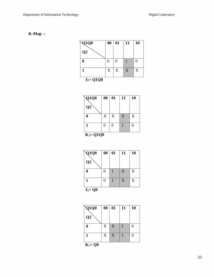
Department of Information Technology Digital Laboratory
34
Q1Q0
Q2
00 01 11 10
0 1 X X 1
1 1 X X 1
J0= 1
Q1Q0
Q2
00 01 11 10
0 X 1 1 X
1 X 1 1 X
K0= 1
Logic Diagram
Fig 1 3 bit Synchronous up counter
Department of Information Technology Digital Laboratory
35
2 3 bit Synchronous down counter
This is used to count from 7-0 ie(111-000)for this also 2 ICrsquos of 74LS76 are required amp hence we use 3
MS JK flip flops Here also clock is given to 1stamp 6th pin of 1st IC amp1st pin of 2nd IC enabling to apply
clock to all flip flop at a time Next state decoder logic is designed with the help of state table
State table for synchronous down counter
Present state Next state Flip flop 3 Flip flop 2 Flip flop 1
Q2 Q1 Q0 Q2 Q1 Q0 J2 K2 J1 K1 J0 K0
1 1 1 1 1 0 X 0 X 0 X 1
1 1 0 1 0 1 X 0 X 1 1 X
1 0 1 1 0 0 X 0 0 X X 1
1 0 0 0 1 1 X 1 1 X 1 X
0 1 1 0 1 0 0 X X 0 X 1
0 1 0 0 0 1 0 X X 1 1 X
0 0 1 0 0 0 0 X 0 X X 1
0 0 0 1 1 1 1 X 1 X 1 X
K-Map
Q1Q0
Q2
00 01 11 10
0 1 0 0 0
1 X X X X
J2= Q1Q0
Q1Q0
Q2
00 01 11 10
Department of Information Technology Digital Laboratory
36
0 X X X X
1 1 0 0 0
K2= Q1Q0
Q1Q0
Q2
00 01 11 10
0 1 0 X X
1 1 0 X X
J1= Q0
Q1Q0
Q2
00 01 11 10
0 X X 0 1
1 X X 0 1
K1= Q0
Q1Q0
Q2
00 01 11 10
0 1 X X 1
1 1 X X 1
J0= 1
Q1Q0
Q2
00 01 11 10
0 X 1 1 X
1 X 1 1 X
K0= 1
Department of Information Technology Digital Laboratory
37
Logic Diagram
Fig 2 3 bit Synchronous down counter
Uses
1 Specially used as the counting devices
2 Used in frequency divider circuit
3 Used in digital voltmeter
4 Used in counter type A to D converter
5 Used for time measurement
6 It helps in counting the no of product coming out from machinery where product is coming out
at equal interval of time
Conclusion
Up and down counters are successfully implemented the counters are studied amp op are checked The
state table is verified
PRACTICE ASSIGNMENTS EXERCISE MODIFICATIONS
1 Design amp implement 2 bit controlled synchronous counter
2 Designamp implement 4 bit controlled synchronous counter
3 Designamp implement truncated synchronous up or down counter
FAQrsquos with answers
1 What do you mean by Counter
A Counter is a register capable of counting the no of clock pulses arriving at its
clock inputs Count represents the no of clock pulses arrived A specified
sequence of states appears as the counter output
Department of Information Technology Digital Laboratory
38
2 What are the types of Counters Explain each
There are two types of counters as Asynchronous Counter and Synchronous Counter
Asynchronous Counter In this counter the first flip-flop is clocked by the external clock pulse
and then each successive flip-flop is clocked by the Q or Qrsquo op of the previous flip-flop Hence in
Asynchronous Counter flip-flops are not clocked simultaneously and hence called as Ripple
Counter Synchronous Counter In this counter the common clock input is connected to all the
flip-flops simultaneously
3 What do you mean by pre-settable counters
A counter in which starting state is not zero can be designed by making use of the
preset inputs of the flip flops This is referred to as loading the counter
asynchronously This is referred to as pre-settable counter
4 What are the applications of synchronous counters
Digital clock
Frequency divider circuits
Frequency counters
Used in analog to digital converters
5 What are the advantages of synchronous counters over asynchronous counters
Propagation delay time is reduced
Can operate at a much higher frequency than the asynchronous counters
6 Ring counter is an example of synchronous counters or asynchronous counter
Synchronous counter Since all the flip flops are clocked simultaneously
7 Twisted Ring (Johnsonrsquos) counter is an example of synchronous counters or asynchronous
counter
Synchronous counter Since all the flip flops are clocked simultaneously
8 What is the difference between ring counter and twisted ring counter
In ring counter pulses to be counted are applied to a counter it goes from state to state and the
output of the flip flop s in the counter is decoded to read the count Here the uncomplimentary
output (Q) of last flip flop is fed back as an input to first flip flop Ring counters are referred as
MOD lsquoNrsquo counters
Department of Information Technology Digital Laboratory
39
But in Twisted ring counter the complimentary output (Q bar) of last flip flop is fed back as an
input to first flip flop Twisted Ring counters are referred as MOD lsquo2Nrsquo counters
9 What are the applications of ring counters
Ring counter outputs are sequential non-overlapping pulses which are useful for control state
counters Used in stepper motor this requires pulses to rotate it from one position to the next Used
as divide by lsquoNrsquo ((MOD lsquoNrsquo) counters
10 What are the applications of ring counter twisted ring counters
Used as divide by lsquo2Nrsquo ((MOD lsquo2Nrsquo) counters
Used for control state counters
Used for generation of multiphase clock
11 List the Synchronous Counter ICs
IC 74160 Decade Up Counter
IC 74161 4 bit binary Up Counter
IC 74162 Decade Up Counter
IC 74163 4 bit binary Up Counter
IC 74168 Decade UpDown Counter
IC 74169 4 bit Binary UpDown Counter
IC 74190 Decade UpDown Counter
IC 74191 4 bit Binary UpDown Counter
IC 74192 Decade UpDown Counter
IC 74193 4 bit Binary UpDown Counter
Department of Information Technology Digital Laboratory
40
Regularity Content Viva-voce Timely
Submission Total
Dated Sign of
Subject
Teacher
2 4 2 2 10
Date of Performance Date of Completion
-------------------------------------------------------------------------------------------------------------------
Assignment No 5
-------------------------------------------------------------------------------------------------------------------------------
Title Design and implementation of Module lsquonrsquo counter with IC7490 and IC 74191
-----------------------------------------------------------------------------------------------------------------------------
Objective To know difference between regular amp truncated counter as well as binary ampBCD Counter
--------------------------------------------------------------------------------------------------------------------------------
Problem Statement To design and implement mod - 10 mod ndash 7 mod - 99 asynchronous BCD
counter using IC 7490 and to design and implement up down mod - n Binary counter using IC 74191
-----------------------------------------------------------------------------------------------------------------
Hardware Requirement
i) IC 7490 IC 74191 basic gates
ii) Digital Trainer Kit -1
iii) Patch cords
----------------------------------------------------------------------------------------------------------------
Software Requirement Digital Work 30
------------------------------------------------------------------------------------------------------------------
Theory
Part A ndash IC 7490
IC 7490 is a TTL MSI (medium scale integration) decade counter It contains 4 master slave flip flops
internally connected to provide MOD-2 ie divide by 2 and MOD-5 ie divide by 5 counters MOD-2 and
Mod-5 counters can be used independently or in cascading
Department of Information Technology Digital Laboratory
41
It is a 4-bit ripple type decade counter The device consists of 4-master slave flip flops internally
connected to provide a divide by two and divide by 5 sections Each section has a separate clock ip to
initiate state changes of the counter on the high to low clock transition
Since the op from the divide by 2 section is not internally connected to the succeeding stages The device
may be operated in various counting modes In a BCD counter the CP1 input must be externally connected
to QA op The CP0ip receives the incoming count producing a BCD count sequence It is also provided
with additional gating to provide a divide by 2 counter and binary counter for which the count cycle length
is divide by 5 The device may be operated in various counting modes
There are 2 reset inputs R0(1) and R0(2) both of which need to be connected to the lsquologic 1rsquo for clearing all
flip flops Two set inputs Rg(1) and Rg(2) when connected to logic 1 are used for setting counter to 1001
(BCD 9)
Pin out of IC 7490
Fig Pin configuration of IC7490
Table 1-pin name and description of IC7490
Pin name Description
Input B This is clock input to the internal MOD-5 ripple counter which is negative
edge triggered
R0(1)R0(2) Gated zero reset inputs
Department of Information Technology Digital Laboratory
42
R9(1)R9(2) These are gated set to nine inputs
QDQCQB Output of internal MOD-5 counter with QD as MSB
QA Output of internal MOD-2 counter with QA as LSB
Input A Clock input to FF-A which is negative edge triggered
Functional Table for IC7490
Reset inputs Output
R0(1) R0(2) R9(0) R9(1) QD QC QB QA
1 1 0 X 0 0 0 0
1 1 X 0 0 0 0 0
X X 1 1 1 0 0 1
X 0 X 0 COUNTER
0 X 0 X COUNTER
0 X X 0 COUNTER
X 0 0 x COUNTER
Department of Information Technology Digital Laboratory
43
Basic internal Structure of IC 7490
Function Table of MOD-5 counter
Design of MOD-10 counter using IC 7490
The QA op the first flip flop is connected to the input B which is clock ip of internal MOD-5 ripple
counter Due to cascading of Mod-2 and Mod-5 counters the overall configuration the decade counters
count from 0000 to 1001 After 1001 mod-5 resets to 0000 and next count after 1001 is 0000
When QA op is connected to B ip we have the Mod-2 counter followed by Mod-5 counter The
count sequence obtained is shown in the table It may be noted that QA changes from 0 to 1 the state of
InputB clock Output
Count QD QC QB
0 0 0 0
0 0 1 1
0 1 0 2
0 1 1 3
1 0 0 4
Department of Information Technology Digital Laboratory
44
Mod-5 counter doesnrsquot change whereas when QA changes from 1 to 0 the Mod-5 counter goes to the next
state
Logic DiagramMOD-10 counter using IC 7490
5 Modulus n Counter
Function table
Ip clock
Output
Count QD QC QB QA
0 0 0 0 0
0 0 0 1 1
0 0 1 0 2
0 0 1 1 3
0 1 0 0 4
Department of Information Technology Digital Laboratory
45
Design of Mod-7 Counter using IC 7490
Mod-7 counter counts through seven states from 0 to 6 counters and it should reset as soon as the
count becomes 7 The op of reset logic should be 1 corresponding to invalid states The reset logic op
should be applied to pin 2 and 3
Truth Table of Reset Logic
0 1 0 1 5
0 1 1 0 6
0 1 1 1 7
1 0 0 0 8
1 0 0 1 9
QD QC QB QA Y
0 0 0 0 0
0 0 0 1 0
0 0 1 0 0
0 0 1 1 0
0 1 0 0 0
0 1 0 1 0
0 1 1 0 0
0 1 1 1 1
1 0 0 0 1
1 0 0 1 1
Department of Information Technology Digital Laboratory
46
Logic Diagram Mod 7 Counter using IC 7490
Function table
Ip clock
Output
Count QD QC QB QA
0 0 0 0 0
0 0 0 1 1
0 0 1 0 2
0 0 1 1 3
0 1 0 0 4
0 1 0 1 5
0 1 1 0 6
Department of Information Technology Digital Laboratory
47
Design of Mod-99 using IC 7490
For Mod-99 two IC 7490rsquos will be required Hence to implement a divide by 99 counter we have
to use two decade counters ICrsquos A divide by 99 counter counts 99 states from 0 to 98 and the counter
should reset as soon as the count becomes 99 So in order to reset the counter of 99 connect the Q op
which are equal to 1 in the count of 99 to an lsquoAndrsquo gate amp then connect and op to the reset ip of both
ICrsquos
MOD-100 Counter-
MOD-100 counter can be obtained by cascading two decade counter ICrsquos
Each IC gives divide by 10 counts Hence 2 ICs will give 1010=100 counts
Clock is applied to the input A of IC 7490 the Q1 output is connected to B input etc
For cascading the QD output of the first IC is connected to the input A of second IC Thus QD of
IC-(1) acts as clock input to IC-(2)
The Ro (1) Ro(2) R9(1) R9(2) inputs of both ICs are connected to ground so as to make them
inactive
The total count provided by the two counters varies from 00 to 99 decimal that means 100 states
Hence it is a MOD-10 counter
Impleacutementations
FigureMOD-100 counters using IC 7490
Department of Information Technology Digital Laboratory
48
B) IC 74191 ndash Theory
IC74191 is 4-bit binary synchronous reversible up down counter It contains 4 master slave flip flops
with internal gating and steering logic to provide asynchronous reset and synchronous count updown
operations its asynchronous parallel capability permits the counter to be preset to any desire number D0
to D3 are the parallel data inputs Information present on the parallel data inputs D0 to D3 is loaded into
the counter and appears on the output when the load PLinput is lowThisoperation overrides the counting
function Counting is inhabited by the high level on the enable G input when G input is low internal state
changes are initiated synchronously by the low to high transitions of the clock inputs the updown input
signal determines the direction of input
Function Table
Operating
mode
Inputs Outputs
PL UD G CLK Dn
Parallel
load L X X X L L
L X X X H H
Count up H L 0 uarr X Count up
Count
down H H 0 uarr X
Count
down
Hold(No
change) H X H X X No change
Pin details ndash
D0 to D3 input lines PL parallel load
G is Enable input ndash enabling the counting
Q0 to Q3 output lines
Downup determines the direction of counting
Clk clock input for counter
Terminal Count Max(1111) min(0000) For these states signal goes high for 1clock pulse
Ripple clock Clock input for next higher state
Department of Information Technology Digital Laboratory
49
Pin Diagram IC 74191
Up counter- Truth Table
Clk
Pulses QA QB QC QD
0 0 0 0 0
1 0 0 0 1
2 0 0 1 0
3 0 0 1 1
4 0 1 0 0
5 0 1 0 1
6 0 1 1 0
7 1 1 1 1
8 1 0 0 0
9 1 0 0 1
10 1 0 1 0
11 1 0 1 1
12 1 1 0 0
13 1 1 0 1
Department of Information Technology Digital Laboratory
50
14 1 1 1 0
15 1 1 1 1
Logic Diagram
Steps-
Connect the circuit as shown above
Apply clock ip to pin no14
Connect UD to GND
Verify the output according to truth table
Logic diagram of down counter
Steps-
Connect the circuit as shown above
Apply clock ip to pin no14
Connect UD to VCC
Verify the output according to truth table
UD D3 D2 D1 D0 PL
Clock IC 74191
G RC
MAX MIN
Q3 Q2 Q1 Q0 TC
vcc
NC
NC
Outputs
no connection
vcc
Department of Information Technology Digital Laboratory
51
With the help of IC74191 we can implement truncated updown counter by using following logic ndash
Connect data input line to particular count you want to load
According to requirement make Truth table
Draw the K-map
Find out Boolean expression
Draw the logic diagram and that is the combinational logic for your count and apply the output of
that circuit to PL
According to requirement we get the UP and down counting
5 Modulus n Counter
Presettable updown counter
Mod 11 counter
Implementation of presetttable mod updown counter using IC- 74LS191
1 Load Data on data lines D0 to D3 (0101)
2 Counter will go through the states from 0101 0110hellip1111 in up counter and 0101 to 0000 in
down counter
Combinational Circuit
CLOCK D3 D2 D1 D0
TC
U D 74191 RC
G PL
Updown Q3 Q2 Q1 Q0 PL
Q3 Q2 Q1 Q0
Preset Count
Department of Information Technology Digital Laboratory
52
3 The logic circuit should be designed in such a way that only when all the outputs are high output
of the reset circuit should be low and the counter should jump to state 5 It should again start
counting from 0101 to 0000
State Table
Down Counter UP Counter
IC 74191 is 4 bit counter Thus it counts 0000 to 1111 different 16 states For MOD11 counter we require
different 11 states so 5 steps must be skipped from 16 states We get MOD11 by presetting counter to
value 5
Assignment Question
Design and Implement MOD 7 MOD 10 and MOD 12 using IC 74191
FAQs
1 What do you mean modulus counter
Counter
state Clock
pulse
Q3 Q2 Q1 Q0
1 0 1 0 1
2 0 1 1 0
3 0 1 1 1
4 1 0 0 0
5 1 0 0 1
6 1 0 1 0
7 1 0 1 1
8 1 1 0 0
9 1 1 0 1
10 1 1 1 1
11 1 1 1 1
Counter state
Clock pulse
FF outputs
Q3 Q2 Q1 Q0
1 0 1 0 1
2 0 1 0 0
3 0 0 1 1
4 0 0 1 0
5 0 0 0 1
6 0 0 0 0
7 0 1 0 1
Department of Information Technology Digital Laboratory
53
It represents the number of possible states of counter
2 How will you use the 7490 IC to design symmetrical divide by 10 frequency counter
The divide by 5 circuit followed by divide by 2 circuit will give symmetrical output
3Where counters are used Give real life example of counter
Modulus n Counter
Binary counter ndash An N stage counter that recycles after 2 Ncount The count proceds in specified binary
sequence Counter Presetable- A counter which can be set to a desired value before the start of the
counting UPDown counter ndash A counter that can count in both up and down direction depending upon a
control input
Department of Information Technology Digital Laboratory
54
Regularity Content Viva-voce Timely
Submission Total
Dated Sign of
Subject
Teacher
2 4 2 2 10
Date of Performance Date of Completion
-------------------------------------------------------------------------------------------------------------------
Assignment No6
------------------------------------------------------------------------------------------------------------------
Title Sequence Generator
------------------------------------------------------------------------------------------------------------------
Objective To understand sequence generator one of the sequential circuit
-------------------------------------------------------------------------------------------------------------------
Problem Statement Design (State Diagram State Table K Map) and implementation of Sequence
Generator using Shift Register IC 74194
-----------------------------------------------------------------------------------------------------------------
Hardware Requirement
i) IC 741947408 (AND-gate) 7432 (OR-gate)
ii) Digital Trainer Kit -1
iii) Patch cords
----------------------------------------------------------------------------------------------------------------
Software Requirement Digital Work 30
------------------------------------------------------------------------------------------------------------------
Theory
Part A Sequence Generator with Flip flop
A sequential circuit which generates a prescribed sequence of bits in synchronism with a clock is referred
to as a sequence generator These pulse trains or sequence of bits can be used to open valves close gates
turn on lights and turn off machines and other variety of jobs
Department of Information Technology Digital Laboratory
55
For the design of sequence generator we first determine the required no of flip flops and the logic circuit
for the next state decoder
No of flip flops required to generate particular sequence can be determined as follows
1) Find the no of 1rsquos in the sequence
2) Find the no of 0rsquos in the sequence
3) Take the maximum out of two
4) If N is the required no of flip flops choose minimum value of lsquonrsquo to satisfy equation given below
Max (0rsquos 1rsquos) le 2n-1
The sequence generator can be classified as
1) sequence generator without bushing
2) sequence generator with bushing
The aim in this experiment is to design a sequence generator to generate a sequence of bit ie 10101
Part B Sequence Generator using Shift Register IC 74194
IC 74194 4 bit bidirectional Shift Register
This bidirectional shift register is designed to incorporate virtually all the features a system designer may
want in a shift register they feature Parallel inputs parallel outputs right shift left shift serialinputs
operating mode control inputsand a direct overriding clear line The register has four distinct modes of
operationsnamely
1 Parallel load
2 Shift right (in the direction QA towards QD)
3 Shift left (in the direction QD towards QA)
4 Inhibit clock (do nothing)
Synchronous parallel loading is accomplished by applying the four bits of data and taking both
mode control inputs S0 and S1High The data is loaded in to the associated flip-flops and appear
at the outputs after positive transition of the clock input During loading serial data flow is
inhibited
Shift right is accomplished synchronously with the rising edge of the clock pulse when S0 is High
and S1 is Low Serial data for this mode is entered at the shift right data input When S0 is Low
and S1 is High data shifts left synchronously and new data is entered at the shift left serial input
Clocking of the flip flop is inhibited when both mode control inputs are LOW
Department of Information Technology Digital Laboratory
56
Mode Control Input Operation
S1 S0
0 0 Clock Inhibit
0 1 Shift right
1 0 Shift Left
1 1 Parallel loading
Function Table of IC 74194
Design
The minimum number of flip-flops N required to generate a sequence of length S is given by S
le 2N ndash 1
In this case S=7 therefore the minimum value of N which may generate in this sequence is 3
However it is not guaranteed to lead to a solution If the given sequence leads to seven distinct
states then only three flip flops are sufficient otherwise we have to increase the number of flip
flops We write the states of circuit as given in table 1 The prescribed sequence is listed under QA
and the sequence listed under QB and QC are the same sequence delayed by one and two clock
pulses respectively From the table we observe that all the states are not distinct which means N=3
is not sufficient Next we assume that N=4 and prepare table 2 The last column gives the required
serial input for getting the desired change of state when a clock pulse is applied This is obtained
by assuming D type flip flop and looking at the QA output For example at the falling edge of first
clock pulse QA=1 The second clock pulse must result in QA=1 which requires its D input to be 1
In the same manner all the entries in column Y are determined
Table 1 State Assignment Table of Sequence Generator (N=3)
Number of Clock
Pulses
Flip Flop Inputs States
QA QB QC
1 1 1 1 7
2 1 1 1 7
3 0 1 1 3
4 1 0 1 5
Department of Information Technology Digital Laboratory
57
5 0 1 0 2
6 1 0 1 5
7 1 1 0 6
Excitation table of D Flip-Flop
Present State Qn Next State Qn+1 Flip-Flop Input D
0 0 0
0 1 1
1 0 0
1 1 1
Table 2State Assignment Table of Sequence Generator (N=4)
Number of Clock
Pulses
Flip Flop Inputs States
Y
Serial ip QA QB QC QD
1 1 1 1 0 14 1
2 1 1 1 1 15 0
3 0 1 1 1 7 1
4 1 0 1 1 11 0
5 0 1 0 1 5 1
6 1 0 1 0 10 1
7 1 1 0 1 13 1
K-Map Simplification
Department of Information Technology Digital Laboratory
58
00 01 11 10
00 X X X X
01 X 1 1 X
11 X 1 0 1
10 X X 0 1
Y= QArsquo + QBrsquo + QCrsquo = QAQBQC
LOGIC DIAGRAM
HARDWARE REQUIREMENTS
Sr no ICs Description Quantity
11 74194 4 bit bidirectional universal shift register 16ktr`
2 7410 3 input NAND Gate 1
Department of Information Technology Digital Laboratory
59
Conclusion In this way sequence generator using JK flip flips amp shift register is designed and
implemented
Enhancements Modifications ndash Sequence generator can also be implemented with shift register instead
of flip flops Use IC 7495 universal shift register IC and try to implement sequence generator
FAQs
1 What is sequential logic circuit
A sequential logic circuit consists of a memory elements in addition to
combinational circuit Its output at any instant of time depends upon
the present input as well as present state of memory element
2 What is meant by delay line
It is used to introduce time delays in digital signals
3 What is meant by following terms
a) Synchronous preset b) Asynchronous preset
c) Synchronous clear d) Asynchronous clear
a)Preset operation is synchronised with the clock
b)Preset operation is independent of the clock
c) clear is performed in synchronous with clock
d) clear is performed independent with clock
4 Is asynchronous counter faster than synchronous counter
In a synchronous counter the time required for change of any state is same and is equal to delay
time of one flip flop where as in asynchronous counter all flip flops are not clocked
simultaneously hence time required is not same
5 What is mean by lockout in counter
In a counter design for a fewer state than the maximum possible state some time it may so happen
that counter enters in unused state and goes from one unused state to another unused state and
never comes to used state
6 What is mean by state table
Department of Information Technology Digital Laboratory
60
It consists of complete information about present state and next state and outputs of a sequential
system
7 What is mean by state diagram
The information available in a state table can be represented as graphically the graphical
representation is known as state diagram
8 What is the advantage of state reduction in the design of sequential circuit
It reduces the number of flip flops
9 What is meant by excitation table
This gives information about what should be the flip flop inputs if outputs are specified before and
after the clock pulse
10 How many flip flops are required to design sequence generator using Counters
max (0rsquoS1rsquoS) in a given sequence lt= 2(N - 1)
Where N = Number of flip flops
11 How many flip flops are required to design sequence generator using shift registers
Slt= 2N - 1
Where N=Number of flip flops
S= Length of sequence
12 What is Lock out condition How it is avoided
When counter enters into one of the invalid state and after application of pulses remains in invalid
states only i e counter gets locked into invalid state amp this is called as lock out Lock out can be
avoided by providing bushing to all the invalid states in such a way that after application of one or
more clock pulses counter will fall into one of the valid state
Department of Information Technology Digital Laboratory
61
Regularity Content Viva-voce Timely
Submission Total
Dated Sign of
Subject
Teacher
2 4 2 2 10
Date of Performance Date of Completion
-------------------------------------------------------------------------------------------------------------------
Assignment No7
------------------------------------------------------------------------------------------------------------------
Title Multiplexer using Data flow modeling and structural modeling
------------------------------------------------------------------------------------------------------------------
Objective To learn data flow modeling style Its uses and different types of declarations with some
different types of circuits Structure of VHDL program is well discussed with this modeling style
-------------------------------------------------------------------------------------------------------------------
Problem Statement 41 multiplexer using data flow amp structural modeling -
----------------------------------------------------------------------------------------------------------------
Hardware Requirement - NA
----------------------------------------------------------------------------------------------------------------
Software Requirement Xilinx
------------------------------------------------------------------------------------------------------------------
Theory
Data flow style-
In this type of design the view of data as flowing from input to output through a design
An operation is defined in terms of a collection of data transformation expressed as concurrent
statement Each of the statement can be activated when any of its input signal changes its value While
these statements describe the behavior of the circuit a lot of information about its structure can be
extracted from the description as well
Data flow modeling has a set of concurrent assignment statements In the data flow level of abstraction we
describe how information is passed in the circuit The built in operators in VHDL are used in expression
such as AND OR XOR NOT etc
Department of Information Technology Digital Laboratory
62
INPUT
Two select lines S1S0
Four data lines D0 D1 D2 D3
OUTPUT
One output line Y
Functional block diagram of 41 Mux
Fig 41 Multiplexer using Data flow modeling
Function table of 41 Mux
Enable S1 S0 A B C D Y
1 X X X X X X 0
0 0 0 A X X X A
0 0 1 X B X X B
0 1 0 X X C X C
0 1 1 X X X D D
Design steps
Click on Xilinx ISE 92i
Create New project from file menu Ensure top level source is HDL
Select family of devices (usually spartan2E or 3)
Department of Information Technology Digital Laboratory
63
Ensure preferred language is VHDL
Click new source which shows you project details device details
and Synthesis and simulator tools
After finishing project create new source by right clicking in project name with VHDL
module
Complete ports name directions and bus Ensure architecture name is behavioral
After that we will get design summary and detailed reports
Close design summary
Create your code with given modeling style
Go to process window and synthesis to check if any error is there in code Check syntax and
view RTL schematic
Create new source to simulate the code
Right click on source name and create test bench waveform with proper name Ensure the
project is same
Click on combinational circuit in initial timing wizard
Select test bench wave in source window Apply inputs to wave diagram Ensure you are in
behavioral simulation
Go to process box Click on Xilinx ISE simulator and simulate the model See results
RTL Schematic
Department of Information Technology Digital Laboratory
64
Timing Diagram
FAQrsquos
1 What are the different kinds of data objects in VHDL code
Ans data object may be any value or number still some signal data objects and bit and bit_vector
types of these are available in VHDL STD_LOGIC and STD_LOGIC_VECTOR types are used
widely in programming
2 What do you mean by signal
Ans signal is a data object represents logic signals or wires in a circuit There are three places in
which signals can be declared in VHDL code in an entity declaration in the declarative section of
architecture and in declarative section of package
3 What are different signal types
Ans BIT BIT_VECTOR STD_LOGIC STD_LOGIC_VECTOR STD_ULOGIC SIGNED
UNSIGNED INTEGER ENUMERATION and BOOLEAN
4 What is an entity
Ans a circuit or sub circuit described with VHDL code is called a design entity
5 Explain structure of an entity
Ans it has two main parts the entity declaration which specifies the input and output signals for
entity and the architecture which gives circuit details
Department of Information Technology Digital Laboratory
65
6 How will you declare a package with component Explain structure
The general form of package declaration is as shown in diagram
PACKAGE package_name IS
[TYPE declarations]
[SIGNAL declarations]
[COMPONENT declarations]
END package_name
Entity
Declaration Architecture
Department of Information Technology Digital Laboratory
66
Regularity Content Viva-voce Timely
Submission Total
Dated Sign of
Subject
Teacher
2 4 2 2 10
Date of Performance Date of Completion
-------------------------------------------------------------------------------------------------------------------
Assignment No8
------------------------------------------------------------------------------------------------------------------
Title Full Adder using Behavioral and Structural modeling
------------------------------------------------------------------------------------------------------------------
Objective To learn structural modeling style Its uses and different types of declarations with some
different types of circuits Structure of VHDL program is well discussed with this modeling style
-------------------------------------------------------------------------------------------------------------------
Problem Statement Full adder using behavioral amp structural modeling
-----------------------------------------------------------------------------------------------------------------
Hardware Requirement - NA
----------------------------------------------------------------------------------------------------------------
Software Requirement Xilinx
------------------------------------------------------------------------------------------------------------------
Theory
Structural style-
A digital electronic system can be described as a module with inputs andor outputs The electrical values
on the outputs are same functions of the values of inputs The example of it is as shown The NAND gate
has 2ips AampB amp an output y Using VHDL terminology we call the NAND2 design entity amp the inputs
amp outputs are called ports 1 way of describing the function of NAND2 is to describe how it is composed
of sub modules AND amp INVERTER Each of the Sub modules is an instance of some entity amp ports of the
instances are connected using signals Structural modeling has a set of interconnected component
Structure can be used to create a very low level description of a circuit or a very high level description
Department of Information Technology Digital Laboratory
67
In a gate level description of a circuit for example components such as basic logic gates amp FFs might be
connected in some logical stricture to create the circuit This is what is often called a net list
Structure of structural modeling
Functional block diagram of Full Adder
architectureNetlistofHalf_Adderis
-- component with locals
componentMyXorport (A_XorB_Xor in BIT
Z_Xor out BIT)
end component
-- component with locals
componentMyAndport (A_AndB_And in BIT
Z_And out BIT)
end component
begin
Xor1 MyXorport map (X Y Sum)
-- instance with actuals
And1 MyAndport map (X Y Cout)
-- instance with actuals
end
Department of Information Technology Digital Laboratory
68
Function table of Full Adder
A B Cin SUM CARRY
0 0 0 0 0
0 0 1 1 0
0 1 0 1 0
0 1 1 0 1
1 0 0 1 0
1 0 1 0 1
1 1 0 0 1
1 1 1 1 1
Sum = Σm(1 2 4 7)
Carry= Σm(3 5 6 7)
Design steps
Click on Xilinx ISE 92i
Create New project from file menu Ensure top level source is HDL
Select family of devices (usually spartan2E or 3)
Ensure preferred language is VHDL
Click new source which shows you project details device details
and Synthesis and simulator tools
After finishing project create new source(full adder) by right clicking in project name with
VHDL module
Complete ports name directions and bus Ensure architecture name is behavioral
After that we will get design summary and detailed reports
Close design summary
Click new source which shows you project details device details
and Synthesis and simulator tools
After finishing project create new source(half adder) by right clicking in project name with
VHDL module
Complete ports name directions and bus Ensure architecture name is behavioral Names
should be same as previous inputs
Department of Information Technology Digital Laboratory
69
After that we will get design summary and detailed reports
Close design summary
Create your code for half adder with given modeling style
After that go to process window Click on design utilities
View HDL instantiation code of half adder
Copy component part of half adder in architecture block of full adder Copy instantiation
template twice after begin as we require two half adders to construct full adder (structural
modeling) Name them differently (eg ha1 or ha2)
Create signals as per the logic Complete code of full adder
Go to process window and synthesis to check if any error is there in code Check syntax and
view RTL schematic
Create new source to simulate the code
Right click on source name and create test bench waveform with proper name Ensure the
project is same
Click on combinational circuit in initial timing wizard
Select test bench wave in source window Apply inputs to wave diagram Ensure you are in
behavioral simulation
Go to process box Click on Xilinx ISE simulator and simulate the model See results
RTL Schematic
Timing Diagram
Department of Information Technology Digital Laboratory
70
INPUT
Three inputs A B Carry (previous)
OUTPUT
Two outputs Sum Carry
FAQrsquos
1 What do you mean by structural style
Ans in this type of code a circuit is described in hierarchical fashion by connecting together sub
circuits
2 Explain IF statement with example
Ans The general form of an IF statement is as follws
IF Sel=rsquo0rsquo THEN
Flt=x1
ELSE
Flt=x2
END IF
Department of Information Technology Digital Laboratory
71
3 Explain declaration and instantiation process in VHDL
Ans first declare a small vhdl code in formal way Eg half adder Define project name is full adder
And simply copy instantiation template in main source code Define how many times you want to
declare this template Give separate names for those
4 What is STD_LOGIC_VECTOR
Ans It is standard data object added to VHDL standard in IEEE 1164 It provides more flexibility
than the Bit type
5 Explain difference between concurrent and sequential statements
Ans Concurrent statements define interconnected processes and blocks that together describe a designrsquos
overall behavior or structure They can be grouped using block sstatement Groups of blocks can also be
partitioned into other blocks At this same level a VHDL component can be connected to define signals
within the blocks
It is a reference to an entity A process can be a single signal assignment statement or a series of
sequential statements (SS) Within a process procedures and functions can partition the sequential
statements
PRACTICE ASSIGNMENTS
1 Implement half adder using data flow modeling
2 Implement Full Adder using behavioral modeling
3 Implement 3 bit magnitude comparator using a 3 bit adder
4 Implement half sub tractor using data flow modeling
5 Write VHDL code for Full Subtractor
Department of Information Technology Digital Laboratory
72
Regularity Content Viva-voce Timely
Submission Total
Dated Sign of
Subject
Teacher
2 4 2 2 10
rsquozaDate of Performance Date of Completion
-------------------------------------------------------------------------------------------------------------------
Assignment No9
------------------------------------------------------------------------------------------------------------------
Title Simulation of 3 bit Connter using Behavioral modeling
------------------------------------------------------------------------------------------------------------------
Objective To learn behavioral modeling style Its uses and different types of declarations with some
different types of circuits Structure of VHDL program is well discussed with this modeling style
-------------------------------------------------------------------------------------------------------------------
Problem Statement 3 bit controlled up down synchronous counter with preset amp clear
-----------------------------------------------------------------------------------------------------------------
Hardware Requirement -NA
----------------------------------------------------------------------------------------------------------------
Software Requirement Xilinx
------------------------------------------------------------------------------------------------------------------
Theory
Behavioral style-
Highest level of abstraction supported in VHDL is called the behavior level of abstraction In it we have
for loop while loop If then else case ampvariable assignment The statements are enclosed in a PROCESS
block amp are executed sequentially
In it circuit is described in terms of its operation overtime
In behavioral description the concept of time may be expressed precisely with actual delays between
related events (such as the propagation delays within gates amp on wires) or it may be simply an ordering of
operation that are expressed sequentially (such as in a functional description of a FF)
Department of Information Technology Digital Laboratory
73
A behavioral design method defines a circuit in terms of text language rather than a schematic of
interconnected symbols
Behavioral design is a technology independent text based design that incorporates high level
functionality amp high level information flow
Structure of Behavioral modeling
Functional block diagram of 3 bit controlled up down synchronous counter with preset amp clear
Function table of 3 bit controlled up down synchronous counter with preset amp clear
Design steps
Click on Xilinx ISE 92i
Create New project from file menu Ensure top level source is HDL
Select family of devices (usually spartan2E or 3)
Ensure preferred language is VHDL
Click new source which shows you project details device details
and Synthesis and simulator tools
After finishing project create new source by right clicking in project name with VHDL
module
Complete ports name directions and bus Ensure architecture name is behavioral
After that we will get design summary and detailed reports
Close design summary
Create your code with given modeling style
Go to process window and synthesis to check if any error is there in code Check syntax
and view RTL schematic Create new source to simulate the code
Department of Information Technology Digital Laboratory
74
Right click on source name and create test bench waveform with proper name Ensure the
project is same
Click on combinational circuit in initial timing wizard
Select test bench wave in source window Apply inputs to wave diagram Ensure you are in
behavioral simulation
Go to process box Click on Xilinx ISE simulator and simulate the model
RTL Schematic
Timing Diagram
INPUT
Clock Preset Clear
OUTPUT
Three output lines
FAQrsquos
1 Explain the structure of behavioral modeling
2 What are the differences between behavioral and structural modeling
Ans Behavioral descriptionof a circuit is the highest level of abstraction in VHDL Here the
circuit is described in terms of it operation with respect to time All operations are in one level of
code The operations are described in a way that the designer of a sequential circuit infers a
register
Structural description on the other hand is a circuit description in terms of its components
it can either create a low level description much like a hierarchy in a block diagram Whenever
you see a component instantiated in a code that code employs structural description of the circuit
The components are connected in the form of a netlist This is for better manageability and
reusability
3 What are the differences between behavioral and data flow modeling
Department of Information Technology Digital Laboratory
75
Ans Behavioral ndash describes how the output is derived from the inputs using structured
statements
Dataflow ndash describes how the data flows from the inputs to the output most often
using NOT AND and OR operations
4 What do you mean by process statement
Ans The process statement begins with the PROCESS keyword followed by a parenthesized list
of signals called the sensitivity list It operates on selected and conditional statements
5 Explain syntax of process statement
Ans BEGIN
Process( sensitivity list)
END process
PRACTICE ASSIGNMENTS
1 Implement 3 bit asynchronous up counter using behavioral modeling
2 Implement 3 bit asynchronous down counter using behavioral modeling
3 Implement 3 bit synchronous down counter using behavioral modeling
End
Department of Information Technology Digital Laboratory
76
Pin Diagrams
7400 Quad 2-Input NAND Gate
7402 Quad 2-Input NOR Gate
7404 Not Gates
7408 Quad 2-Input AND Gates
7432 Quad 2-Input OR Gate
7486 Quad 2-Input Exclusive-OR Gate
Department of Information Technology Digital Laboratory
77
7483 4 bit Binary Adder
7490 Decade and Binary Counters
74138 38 Decoder
Department of Information Technology Digital Laboratory
78
74153 Dual 41 Multiplexer
74191 Synchronous UpDown 4 bit Binary counter with Mode Control
Department of Information Technology Digital Laboratory
79
74194 Universal Shift Register
7476 Dual Master-Slave J-K Flip-Flops
- Part B Sequence Generator using Shift Register IC 74194
-
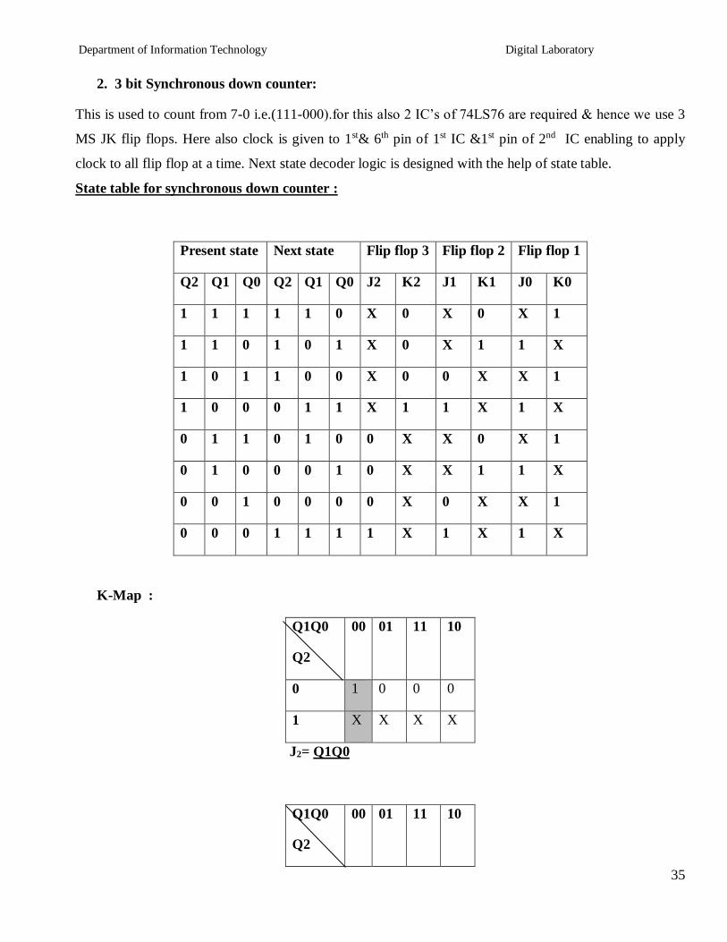
Department of Information Technology Digital Laboratory
35
2 3 bit Synchronous down counter
This is used to count from 7-0 ie(111-000)for this also 2 ICrsquos of 74LS76 are required amp hence we use 3
MS JK flip flops Here also clock is given to 1stamp 6th pin of 1st IC amp1st pin of 2nd IC enabling to apply
clock to all flip flop at a time Next state decoder logic is designed with the help of state table
State table for synchronous down counter
Present state Next state Flip flop 3 Flip flop 2 Flip flop 1
Q2 Q1 Q0 Q2 Q1 Q0 J2 K2 J1 K1 J0 K0
1 1 1 1 1 0 X 0 X 0 X 1
1 1 0 1 0 1 X 0 X 1 1 X
1 0 1 1 0 0 X 0 0 X X 1
1 0 0 0 1 1 X 1 1 X 1 X
0 1 1 0 1 0 0 X X 0 X 1
0 1 0 0 0 1 0 X X 1 1 X
0 0 1 0 0 0 0 X 0 X X 1
0 0 0 1 1 1 1 X 1 X 1 X
K-Map
Q1Q0
Q2
00 01 11 10
0 1 0 0 0
1 X X X X
J2= Q1Q0
Q1Q0
Q2
00 01 11 10
Department of Information Technology Digital Laboratory
36
0 X X X X
1 1 0 0 0
K2= Q1Q0
Q1Q0
Q2
00 01 11 10
0 1 0 X X
1 1 0 X X
J1= Q0
Q1Q0
Q2
00 01 11 10
0 X X 0 1
1 X X 0 1
K1= Q0
Q1Q0
Q2
00 01 11 10
0 1 X X 1
1 1 X X 1
J0= 1
Q1Q0
Q2
00 01 11 10
0 X 1 1 X
1 X 1 1 X
K0= 1
Department of Information Technology Digital Laboratory
37
Logic Diagram
Fig 2 3 bit Synchronous down counter
Uses
1 Specially used as the counting devices
2 Used in frequency divider circuit
3 Used in digital voltmeter
4 Used in counter type A to D converter
5 Used for time measurement
6 It helps in counting the no of product coming out from machinery where product is coming out
at equal interval of time
Conclusion
Up and down counters are successfully implemented the counters are studied amp op are checked The
state table is verified
PRACTICE ASSIGNMENTS EXERCISE MODIFICATIONS
1 Design amp implement 2 bit controlled synchronous counter
2 Designamp implement 4 bit controlled synchronous counter
3 Designamp implement truncated synchronous up or down counter
FAQrsquos with answers
1 What do you mean by Counter
A Counter is a register capable of counting the no of clock pulses arriving at its
clock inputs Count represents the no of clock pulses arrived A specified
sequence of states appears as the counter output
Department of Information Technology Digital Laboratory
38
2 What are the types of Counters Explain each
There are two types of counters as Asynchronous Counter and Synchronous Counter
Asynchronous Counter In this counter the first flip-flop is clocked by the external clock pulse
and then each successive flip-flop is clocked by the Q or Qrsquo op of the previous flip-flop Hence in
Asynchronous Counter flip-flops are not clocked simultaneously and hence called as Ripple
Counter Synchronous Counter In this counter the common clock input is connected to all the
flip-flops simultaneously
3 What do you mean by pre-settable counters
A counter in which starting state is not zero can be designed by making use of the
preset inputs of the flip flops This is referred to as loading the counter
asynchronously This is referred to as pre-settable counter
4 What are the applications of synchronous counters
Digital clock
Frequency divider circuits
Frequency counters
Used in analog to digital converters
5 What are the advantages of synchronous counters over asynchronous counters
Propagation delay time is reduced
Can operate at a much higher frequency than the asynchronous counters
6 Ring counter is an example of synchronous counters or asynchronous counter
Synchronous counter Since all the flip flops are clocked simultaneously
7 Twisted Ring (Johnsonrsquos) counter is an example of synchronous counters or asynchronous
counter
Synchronous counter Since all the flip flops are clocked simultaneously
8 What is the difference between ring counter and twisted ring counter
In ring counter pulses to be counted are applied to a counter it goes from state to state and the
output of the flip flop s in the counter is decoded to read the count Here the uncomplimentary
output (Q) of last flip flop is fed back as an input to first flip flop Ring counters are referred as
MOD lsquoNrsquo counters
Department of Information Technology Digital Laboratory
39
But in Twisted ring counter the complimentary output (Q bar) of last flip flop is fed back as an
input to first flip flop Twisted Ring counters are referred as MOD lsquo2Nrsquo counters
9 What are the applications of ring counters
Ring counter outputs are sequential non-overlapping pulses which are useful for control state
counters Used in stepper motor this requires pulses to rotate it from one position to the next Used
as divide by lsquoNrsquo ((MOD lsquoNrsquo) counters
10 What are the applications of ring counter twisted ring counters
Used as divide by lsquo2Nrsquo ((MOD lsquo2Nrsquo) counters
Used for control state counters
Used for generation of multiphase clock
11 List the Synchronous Counter ICs
IC 74160 Decade Up Counter
IC 74161 4 bit binary Up Counter
IC 74162 Decade Up Counter
IC 74163 4 bit binary Up Counter
IC 74168 Decade UpDown Counter
IC 74169 4 bit Binary UpDown Counter
IC 74190 Decade UpDown Counter
IC 74191 4 bit Binary UpDown Counter
IC 74192 Decade UpDown Counter
IC 74193 4 bit Binary UpDown Counter
Department of Information Technology Digital Laboratory
40
Regularity Content Viva-voce Timely
Submission Total
Dated Sign of
Subject
Teacher
2 4 2 2 10
Date of Performance Date of Completion
-------------------------------------------------------------------------------------------------------------------
Assignment No 5
-------------------------------------------------------------------------------------------------------------------------------
Title Design and implementation of Module lsquonrsquo counter with IC7490 and IC 74191
-----------------------------------------------------------------------------------------------------------------------------
Objective To know difference between regular amp truncated counter as well as binary ampBCD Counter
--------------------------------------------------------------------------------------------------------------------------------
Problem Statement To design and implement mod - 10 mod ndash 7 mod - 99 asynchronous BCD
counter using IC 7490 and to design and implement up down mod - n Binary counter using IC 74191
-----------------------------------------------------------------------------------------------------------------
Hardware Requirement
i) IC 7490 IC 74191 basic gates
ii) Digital Trainer Kit -1
iii) Patch cords
----------------------------------------------------------------------------------------------------------------
Software Requirement Digital Work 30
------------------------------------------------------------------------------------------------------------------
Theory
Part A ndash IC 7490
IC 7490 is a TTL MSI (medium scale integration) decade counter It contains 4 master slave flip flops
internally connected to provide MOD-2 ie divide by 2 and MOD-5 ie divide by 5 counters MOD-2 and
Mod-5 counters can be used independently or in cascading
Department of Information Technology Digital Laboratory
41
It is a 4-bit ripple type decade counter The device consists of 4-master slave flip flops internally
connected to provide a divide by two and divide by 5 sections Each section has a separate clock ip to
initiate state changes of the counter on the high to low clock transition
Since the op from the divide by 2 section is not internally connected to the succeeding stages The device
may be operated in various counting modes In a BCD counter the CP1 input must be externally connected
to QA op The CP0ip receives the incoming count producing a BCD count sequence It is also provided
with additional gating to provide a divide by 2 counter and binary counter for which the count cycle length
is divide by 5 The device may be operated in various counting modes
There are 2 reset inputs R0(1) and R0(2) both of which need to be connected to the lsquologic 1rsquo for clearing all
flip flops Two set inputs Rg(1) and Rg(2) when connected to logic 1 are used for setting counter to 1001
(BCD 9)
Pin out of IC 7490
Fig Pin configuration of IC7490
Table 1-pin name and description of IC7490
Pin name Description
Input B This is clock input to the internal MOD-5 ripple counter which is negative
edge triggered
R0(1)R0(2) Gated zero reset inputs
Department of Information Technology Digital Laboratory
42
R9(1)R9(2) These are gated set to nine inputs
QDQCQB Output of internal MOD-5 counter with QD as MSB
QA Output of internal MOD-2 counter with QA as LSB
Input A Clock input to FF-A which is negative edge triggered
Functional Table for IC7490
Reset inputs Output
R0(1) R0(2) R9(0) R9(1) QD QC QB QA
1 1 0 X 0 0 0 0
1 1 X 0 0 0 0 0
X X 1 1 1 0 0 1
X 0 X 0 COUNTER
0 X 0 X COUNTER
0 X X 0 COUNTER
X 0 0 x COUNTER
Department of Information Technology Digital Laboratory
43
Basic internal Structure of IC 7490
Function Table of MOD-5 counter
Design of MOD-10 counter using IC 7490
The QA op the first flip flop is connected to the input B which is clock ip of internal MOD-5 ripple
counter Due to cascading of Mod-2 and Mod-5 counters the overall configuration the decade counters
count from 0000 to 1001 After 1001 mod-5 resets to 0000 and next count after 1001 is 0000
When QA op is connected to B ip we have the Mod-2 counter followed by Mod-5 counter The
count sequence obtained is shown in the table It may be noted that QA changes from 0 to 1 the state of
InputB clock Output
Count QD QC QB
0 0 0 0
0 0 1 1
0 1 0 2
0 1 1 3
1 0 0 4
Department of Information Technology Digital Laboratory
44
Mod-5 counter doesnrsquot change whereas when QA changes from 1 to 0 the Mod-5 counter goes to the next
state
Logic DiagramMOD-10 counter using IC 7490
5 Modulus n Counter
Function table
Ip clock
Output
Count QD QC QB QA
0 0 0 0 0
0 0 0 1 1
0 0 1 0 2
0 0 1 1 3
0 1 0 0 4
Department of Information Technology Digital Laboratory
45
Design of Mod-7 Counter using IC 7490
Mod-7 counter counts through seven states from 0 to 6 counters and it should reset as soon as the
count becomes 7 The op of reset logic should be 1 corresponding to invalid states The reset logic op
should be applied to pin 2 and 3
Truth Table of Reset Logic
0 1 0 1 5
0 1 1 0 6
0 1 1 1 7
1 0 0 0 8
1 0 0 1 9
QD QC QB QA Y
0 0 0 0 0
0 0 0 1 0
0 0 1 0 0
0 0 1 1 0
0 1 0 0 0
0 1 0 1 0
0 1 1 0 0
0 1 1 1 1
1 0 0 0 1
1 0 0 1 1
Department of Information Technology Digital Laboratory
46
Logic Diagram Mod 7 Counter using IC 7490
Function table
Ip clock
Output
Count QD QC QB QA
0 0 0 0 0
0 0 0 1 1
0 0 1 0 2
0 0 1 1 3
0 1 0 0 4
0 1 0 1 5
0 1 1 0 6
Department of Information Technology Digital Laboratory
47
Design of Mod-99 using IC 7490
For Mod-99 two IC 7490rsquos will be required Hence to implement a divide by 99 counter we have
to use two decade counters ICrsquos A divide by 99 counter counts 99 states from 0 to 98 and the counter
should reset as soon as the count becomes 99 So in order to reset the counter of 99 connect the Q op
which are equal to 1 in the count of 99 to an lsquoAndrsquo gate amp then connect and op to the reset ip of both
ICrsquos
MOD-100 Counter-
MOD-100 counter can be obtained by cascading two decade counter ICrsquos
Each IC gives divide by 10 counts Hence 2 ICs will give 1010=100 counts
Clock is applied to the input A of IC 7490 the Q1 output is connected to B input etc
For cascading the QD output of the first IC is connected to the input A of second IC Thus QD of
IC-(1) acts as clock input to IC-(2)
The Ro (1) Ro(2) R9(1) R9(2) inputs of both ICs are connected to ground so as to make them
inactive
The total count provided by the two counters varies from 00 to 99 decimal that means 100 states
Hence it is a MOD-10 counter
Impleacutementations
FigureMOD-100 counters using IC 7490
Department of Information Technology Digital Laboratory
48
B) IC 74191 ndash Theory
IC74191 is 4-bit binary synchronous reversible up down counter It contains 4 master slave flip flops
with internal gating and steering logic to provide asynchronous reset and synchronous count updown
operations its asynchronous parallel capability permits the counter to be preset to any desire number D0
to D3 are the parallel data inputs Information present on the parallel data inputs D0 to D3 is loaded into
the counter and appears on the output when the load PLinput is lowThisoperation overrides the counting
function Counting is inhabited by the high level on the enable G input when G input is low internal state
changes are initiated synchronously by the low to high transitions of the clock inputs the updown input
signal determines the direction of input
Function Table
Operating
mode
Inputs Outputs
PL UD G CLK Dn
Parallel
load L X X X L L
L X X X H H
Count up H L 0 uarr X Count up
Count
down H H 0 uarr X
Count
down
Hold(No
change) H X H X X No change
Pin details ndash
D0 to D3 input lines PL parallel load
G is Enable input ndash enabling the counting
Q0 to Q3 output lines
Downup determines the direction of counting
Clk clock input for counter
Terminal Count Max(1111) min(0000) For these states signal goes high for 1clock pulse
Ripple clock Clock input for next higher state
Department of Information Technology Digital Laboratory
49
Pin Diagram IC 74191
Up counter- Truth Table
Clk
Pulses QA QB QC QD
0 0 0 0 0
1 0 0 0 1
2 0 0 1 0
3 0 0 1 1
4 0 1 0 0
5 0 1 0 1
6 0 1 1 0
7 1 1 1 1
8 1 0 0 0
9 1 0 0 1
10 1 0 1 0
11 1 0 1 1
12 1 1 0 0
13 1 1 0 1
Department of Information Technology Digital Laboratory
50
14 1 1 1 0
15 1 1 1 1
Logic Diagram
Steps-
Connect the circuit as shown above
Apply clock ip to pin no14
Connect UD to GND
Verify the output according to truth table
Logic diagram of down counter
Steps-
Connect the circuit as shown above
Apply clock ip to pin no14
Connect UD to VCC
Verify the output according to truth table
UD D3 D2 D1 D0 PL
Clock IC 74191
G RC
MAX MIN
Q3 Q2 Q1 Q0 TC
vcc
NC
NC
Outputs
no connection
vcc
Department of Information Technology Digital Laboratory
51
With the help of IC74191 we can implement truncated updown counter by using following logic ndash
Connect data input line to particular count you want to load
According to requirement make Truth table
Draw the K-map
Find out Boolean expression
Draw the logic diagram and that is the combinational logic for your count and apply the output of
that circuit to PL
According to requirement we get the UP and down counting
5 Modulus n Counter
Presettable updown counter
Mod 11 counter
Implementation of presetttable mod updown counter using IC- 74LS191
1 Load Data on data lines D0 to D3 (0101)
2 Counter will go through the states from 0101 0110hellip1111 in up counter and 0101 to 0000 in
down counter
Combinational Circuit
CLOCK D3 D2 D1 D0
TC
U D 74191 RC
G PL
Updown Q3 Q2 Q1 Q0 PL
Q3 Q2 Q1 Q0
Preset Count
Department of Information Technology Digital Laboratory
52
3 The logic circuit should be designed in such a way that only when all the outputs are high output
of the reset circuit should be low and the counter should jump to state 5 It should again start
counting from 0101 to 0000
State Table
Down Counter UP Counter
IC 74191 is 4 bit counter Thus it counts 0000 to 1111 different 16 states For MOD11 counter we require
different 11 states so 5 steps must be skipped from 16 states We get MOD11 by presetting counter to
value 5
Assignment Question
Design and Implement MOD 7 MOD 10 and MOD 12 using IC 74191
FAQs
1 What do you mean modulus counter
Counter
state Clock
pulse
Q3 Q2 Q1 Q0
1 0 1 0 1
2 0 1 1 0
3 0 1 1 1
4 1 0 0 0
5 1 0 0 1
6 1 0 1 0
7 1 0 1 1
8 1 1 0 0
9 1 1 0 1
10 1 1 1 1
11 1 1 1 1
Counter state
Clock pulse
FF outputs
Q3 Q2 Q1 Q0
1 0 1 0 1
2 0 1 0 0
3 0 0 1 1
4 0 0 1 0
5 0 0 0 1
6 0 0 0 0
7 0 1 0 1
Department of Information Technology Digital Laboratory
53
It represents the number of possible states of counter
2 How will you use the 7490 IC to design symmetrical divide by 10 frequency counter
The divide by 5 circuit followed by divide by 2 circuit will give symmetrical output
3Where counters are used Give real life example of counter
Modulus n Counter
Binary counter ndash An N stage counter that recycles after 2 Ncount The count proceds in specified binary
sequence Counter Presetable- A counter which can be set to a desired value before the start of the
counting UPDown counter ndash A counter that can count in both up and down direction depending upon a
control input
Department of Information Technology Digital Laboratory
54
Regularity Content Viva-voce Timely
Submission Total
Dated Sign of
Subject
Teacher
2 4 2 2 10
Date of Performance Date of Completion
-------------------------------------------------------------------------------------------------------------------
Assignment No6
------------------------------------------------------------------------------------------------------------------
Title Sequence Generator
------------------------------------------------------------------------------------------------------------------
Objective To understand sequence generator one of the sequential circuit
-------------------------------------------------------------------------------------------------------------------
Problem Statement Design (State Diagram State Table K Map) and implementation of Sequence
Generator using Shift Register IC 74194
-----------------------------------------------------------------------------------------------------------------
Hardware Requirement
i) IC 741947408 (AND-gate) 7432 (OR-gate)
ii) Digital Trainer Kit -1
iii) Patch cords
----------------------------------------------------------------------------------------------------------------
Software Requirement Digital Work 30
------------------------------------------------------------------------------------------------------------------
Theory
Part A Sequence Generator with Flip flop
A sequential circuit which generates a prescribed sequence of bits in synchronism with a clock is referred
to as a sequence generator These pulse trains or sequence of bits can be used to open valves close gates
turn on lights and turn off machines and other variety of jobs
Department of Information Technology Digital Laboratory
55
For the design of sequence generator we first determine the required no of flip flops and the logic circuit
for the next state decoder
No of flip flops required to generate particular sequence can be determined as follows
1) Find the no of 1rsquos in the sequence
2) Find the no of 0rsquos in the sequence
3) Take the maximum out of two
4) If N is the required no of flip flops choose minimum value of lsquonrsquo to satisfy equation given below
Max (0rsquos 1rsquos) le 2n-1
The sequence generator can be classified as
1) sequence generator without bushing
2) sequence generator with bushing
The aim in this experiment is to design a sequence generator to generate a sequence of bit ie 10101
Part B Sequence Generator using Shift Register IC 74194
IC 74194 4 bit bidirectional Shift Register
This bidirectional shift register is designed to incorporate virtually all the features a system designer may
want in a shift register they feature Parallel inputs parallel outputs right shift left shift serialinputs
operating mode control inputsand a direct overriding clear line The register has four distinct modes of
operationsnamely
1 Parallel load
2 Shift right (in the direction QA towards QD)
3 Shift left (in the direction QD towards QA)
4 Inhibit clock (do nothing)
Synchronous parallel loading is accomplished by applying the four bits of data and taking both
mode control inputs S0 and S1High The data is loaded in to the associated flip-flops and appear
at the outputs after positive transition of the clock input During loading serial data flow is
inhibited
Shift right is accomplished synchronously with the rising edge of the clock pulse when S0 is High
and S1 is Low Serial data for this mode is entered at the shift right data input When S0 is Low
and S1 is High data shifts left synchronously and new data is entered at the shift left serial input
Clocking of the flip flop is inhibited when both mode control inputs are LOW
Department of Information Technology Digital Laboratory
56
Mode Control Input Operation
S1 S0
0 0 Clock Inhibit
0 1 Shift right
1 0 Shift Left
1 1 Parallel loading
Function Table of IC 74194
Design
The minimum number of flip-flops N required to generate a sequence of length S is given by S
le 2N ndash 1
In this case S=7 therefore the minimum value of N which may generate in this sequence is 3
However it is not guaranteed to lead to a solution If the given sequence leads to seven distinct
states then only three flip flops are sufficient otherwise we have to increase the number of flip
flops We write the states of circuit as given in table 1 The prescribed sequence is listed under QA
and the sequence listed under QB and QC are the same sequence delayed by one and two clock
pulses respectively From the table we observe that all the states are not distinct which means N=3
is not sufficient Next we assume that N=4 and prepare table 2 The last column gives the required
serial input for getting the desired change of state when a clock pulse is applied This is obtained
by assuming D type flip flop and looking at the QA output For example at the falling edge of first
clock pulse QA=1 The second clock pulse must result in QA=1 which requires its D input to be 1
In the same manner all the entries in column Y are determined
Table 1 State Assignment Table of Sequence Generator (N=3)
Number of Clock
Pulses
Flip Flop Inputs States
QA QB QC
1 1 1 1 7
2 1 1 1 7
3 0 1 1 3
4 1 0 1 5
Department of Information Technology Digital Laboratory
57
5 0 1 0 2
6 1 0 1 5
7 1 1 0 6
Excitation table of D Flip-Flop
Present State Qn Next State Qn+1 Flip-Flop Input D
0 0 0
0 1 1
1 0 0
1 1 1
Table 2State Assignment Table of Sequence Generator (N=4)
Number of Clock
Pulses
Flip Flop Inputs States
Y
Serial ip QA QB QC QD
1 1 1 1 0 14 1
2 1 1 1 1 15 0
3 0 1 1 1 7 1
4 1 0 1 1 11 0
5 0 1 0 1 5 1
6 1 0 1 0 10 1
7 1 1 0 1 13 1
K-Map Simplification
Department of Information Technology Digital Laboratory
58
00 01 11 10
00 X X X X
01 X 1 1 X
11 X 1 0 1
10 X X 0 1
Y= QArsquo + QBrsquo + QCrsquo = QAQBQC
LOGIC DIAGRAM
HARDWARE REQUIREMENTS
Sr no ICs Description Quantity
11 74194 4 bit bidirectional universal shift register 16ktr`
2 7410 3 input NAND Gate 1
Department of Information Technology Digital Laboratory
59
Conclusion In this way sequence generator using JK flip flips amp shift register is designed and
implemented
Enhancements Modifications ndash Sequence generator can also be implemented with shift register instead
of flip flops Use IC 7495 universal shift register IC and try to implement sequence generator
FAQs
1 What is sequential logic circuit
A sequential logic circuit consists of a memory elements in addition to
combinational circuit Its output at any instant of time depends upon
the present input as well as present state of memory element
2 What is meant by delay line
It is used to introduce time delays in digital signals
3 What is meant by following terms
a) Synchronous preset b) Asynchronous preset
c) Synchronous clear d) Asynchronous clear
a)Preset operation is synchronised with the clock
b)Preset operation is independent of the clock
c) clear is performed in synchronous with clock
d) clear is performed independent with clock
4 Is asynchronous counter faster than synchronous counter
In a synchronous counter the time required for change of any state is same and is equal to delay
time of one flip flop where as in asynchronous counter all flip flops are not clocked
simultaneously hence time required is not same
5 What is mean by lockout in counter
In a counter design for a fewer state than the maximum possible state some time it may so happen
that counter enters in unused state and goes from one unused state to another unused state and
never comes to used state
6 What is mean by state table
Department of Information Technology Digital Laboratory
60
It consists of complete information about present state and next state and outputs of a sequential
system
7 What is mean by state diagram
The information available in a state table can be represented as graphically the graphical
representation is known as state diagram
8 What is the advantage of state reduction in the design of sequential circuit
It reduces the number of flip flops
9 What is meant by excitation table
This gives information about what should be the flip flop inputs if outputs are specified before and
after the clock pulse
10 How many flip flops are required to design sequence generator using Counters
max (0rsquoS1rsquoS) in a given sequence lt= 2(N - 1)
Where N = Number of flip flops
11 How many flip flops are required to design sequence generator using shift registers
Slt= 2N - 1
Where N=Number of flip flops
S= Length of sequence
12 What is Lock out condition How it is avoided
When counter enters into one of the invalid state and after application of pulses remains in invalid
states only i e counter gets locked into invalid state amp this is called as lock out Lock out can be
avoided by providing bushing to all the invalid states in such a way that after application of one or
more clock pulses counter will fall into one of the valid state
Department of Information Technology Digital Laboratory
61
Regularity Content Viva-voce Timely
Submission Total
Dated Sign of
Subject
Teacher
2 4 2 2 10
Date of Performance Date of Completion
-------------------------------------------------------------------------------------------------------------------
Assignment No7
------------------------------------------------------------------------------------------------------------------
Title Multiplexer using Data flow modeling and structural modeling
------------------------------------------------------------------------------------------------------------------
Objective To learn data flow modeling style Its uses and different types of declarations with some
different types of circuits Structure of VHDL program is well discussed with this modeling style
-------------------------------------------------------------------------------------------------------------------
Problem Statement 41 multiplexer using data flow amp structural modeling -
----------------------------------------------------------------------------------------------------------------
Hardware Requirement - NA
----------------------------------------------------------------------------------------------------------------
Software Requirement Xilinx
------------------------------------------------------------------------------------------------------------------
Theory
Data flow style-
In this type of design the view of data as flowing from input to output through a design
An operation is defined in terms of a collection of data transformation expressed as concurrent
statement Each of the statement can be activated when any of its input signal changes its value While
these statements describe the behavior of the circuit a lot of information about its structure can be
extracted from the description as well
Data flow modeling has a set of concurrent assignment statements In the data flow level of abstraction we
describe how information is passed in the circuit The built in operators in VHDL are used in expression
such as AND OR XOR NOT etc
Department of Information Technology Digital Laboratory
62
INPUT
Two select lines S1S0
Four data lines D0 D1 D2 D3
OUTPUT
One output line Y
Functional block diagram of 41 Mux
Fig 41 Multiplexer using Data flow modeling
Function table of 41 Mux
Enable S1 S0 A B C D Y
1 X X X X X X 0
0 0 0 A X X X A
0 0 1 X B X X B
0 1 0 X X C X C
0 1 1 X X X D D
Design steps
Click on Xilinx ISE 92i
Create New project from file menu Ensure top level source is HDL
Select family of devices (usually spartan2E or 3)
Department of Information Technology Digital Laboratory
63
Ensure preferred language is VHDL
Click new source which shows you project details device details
and Synthesis and simulator tools
After finishing project create new source by right clicking in project name with VHDL
module
Complete ports name directions and bus Ensure architecture name is behavioral
After that we will get design summary and detailed reports
Close design summary
Create your code with given modeling style
Go to process window and synthesis to check if any error is there in code Check syntax and
view RTL schematic
Create new source to simulate the code
Right click on source name and create test bench waveform with proper name Ensure the
project is same
Click on combinational circuit in initial timing wizard
Select test bench wave in source window Apply inputs to wave diagram Ensure you are in
behavioral simulation
Go to process box Click on Xilinx ISE simulator and simulate the model See results
RTL Schematic
Department of Information Technology Digital Laboratory
64
Timing Diagram
FAQrsquos
1 What are the different kinds of data objects in VHDL code
Ans data object may be any value or number still some signal data objects and bit and bit_vector
types of these are available in VHDL STD_LOGIC and STD_LOGIC_VECTOR types are used
widely in programming
2 What do you mean by signal
Ans signal is a data object represents logic signals or wires in a circuit There are three places in
which signals can be declared in VHDL code in an entity declaration in the declarative section of
architecture and in declarative section of package
3 What are different signal types
Ans BIT BIT_VECTOR STD_LOGIC STD_LOGIC_VECTOR STD_ULOGIC SIGNED
UNSIGNED INTEGER ENUMERATION and BOOLEAN
4 What is an entity
Ans a circuit or sub circuit described with VHDL code is called a design entity
5 Explain structure of an entity
Ans it has two main parts the entity declaration which specifies the input and output signals for
entity and the architecture which gives circuit details
Department of Information Technology Digital Laboratory
65
6 How will you declare a package with component Explain structure
The general form of package declaration is as shown in diagram
PACKAGE package_name IS
[TYPE declarations]
[SIGNAL declarations]
[COMPONENT declarations]
END package_name
Entity
Declaration Architecture
Department of Information Technology Digital Laboratory
66
Regularity Content Viva-voce Timely
Submission Total
Dated Sign of
Subject
Teacher
2 4 2 2 10
Date of Performance Date of Completion
-------------------------------------------------------------------------------------------------------------------
Assignment No8
------------------------------------------------------------------------------------------------------------------
Title Full Adder using Behavioral and Structural modeling
------------------------------------------------------------------------------------------------------------------
Objective To learn structural modeling style Its uses and different types of declarations with some
different types of circuits Structure of VHDL program is well discussed with this modeling style
-------------------------------------------------------------------------------------------------------------------
Problem Statement Full adder using behavioral amp structural modeling
-----------------------------------------------------------------------------------------------------------------
Hardware Requirement - NA
----------------------------------------------------------------------------------------------------------------
Software Requirement Xilinx
------------------------------------------------------------------------------------------------------------------
Theory
Structural style-
A digital electronic system can be described as a module with inputs andor outputs The electrical values
on the outputs are same functions of the values of inputs The example of it is as shown The NAND gate
has 2ips AampB amp an output y Using VHDL terminology we call the NAND2 design entity amp the inputs
amp outputs are called ports 1 way of describing the function of NAND2 is to describe how it is composed
of sub modules AND amp INVERTER Each of the Sub modules is an instance of some entity amp ports of the
instances are connected using signals Structural modeling has a set of interconnected component
Structure can be used to create a very low level description of a circuit or a very high level description
Department of Information Technology Digital Laboratory
67
In a gate level description of a circuit for example components such as basic logic gates amp FFs might be
connected in some logical stricture to create the circuit This is what is often called a net list
Structure of structural modeling
Functional block diagram of Full Adder
architectureNetlistofHalf_Adderis
-- component with locals
componentMyXorport (A_XorB_Xor in BIT
Z_Xor out BIT)
end component
-- component with locals
componentMyAndport (A_AndB_And in BIT
Z_And out BIT)
end component
begin
Xor1 MyXorport map (X Y Sum)
-- instance with actuals
And1 MyAndport map (X Y Cout)
-- instance with actuals
end
Department of Information Technology Digital Laboratory
68
Function table of Full Adder
A B Cin SUM CARRY
0 0 0 0 0
0 0 1 1 0
0 1 0 1 0
0 1 1 0 1
1 0 0 1 0
1 0 1 0 1
1 1 0 0 1
1 1 1 1 1
Sum = Σm(1 2 4 7)
Carry= Σm(3 5 6 7)
Design steps
Click on Xilinx ISE 92i
Create New project from file menu Ensure top level source is HDL
Select family of devices (usually spartan2E or 3)
Ensure preferred language is VHDL
Click new source which shows you project details device details
and Synthesis and simulator tools
After finishing project create new source(full adder) by right clicking in project name with
VHDL module
Complete ports name directions and bus Ensure architecture name is behavioral
After that we will get design summary and detailed reports
Close design summary
Click new source which shows you project details device details
and Synthesis and simulator tools
After finishing project create new source(half adder) by right clicking in project name with
VHDL module
Complete ports name directions and bus Ensure architecture name is behavioral Names
should be same as previous inputs
Department of Information Technology Digital Laboratory
69
After that we will get design summary and detailed reports
Close design summary
Create your code for half adder with given modeling style
After that go to process window Click on design utilities
View HDL instantiation code of half adder
Copy component part of half adder in architecture block of full adder Copy instantiation
template twice after begin as we require two half adders to construct full adder (structural
modeling) Name them differently (eg ha1 or ha2)
Create signals as per the logic Complete code of full adder
Go to process window and synthesis to check if any error is there in code Check syntax and
view RTL schematic
Create new source to simulate the code
Right click on source name and create test bench waveform with proper name Ensure the
project is same
Click on combinational circuit in initial timing wizard
Select test bench wave in source window Apply inputs to wave diagram Ensure you are in
behavioral simulation
Go to process box Click on Xilinx ISE simulator and simulate the model See results
RTL Schematic
Timing Diagram
Department of Information Technology Digital Laboratory
70
INPUT
Three inputs A B Carry (previous)
OUTPUT
Two outputs Sum Carry
FAQrsquos
1 What do you mean by structural style
Ans in this type of code a circuit is described in hierarchical fashion by connecting together sub
circuits
2 Explain IF statement with example
Ans The general form of an IF statement is as follws
IF Sel=rsquo0rsquo THEN
Flt=x1
ELSE
Flt=x2
END IF
Department of Information Technology Digital Laboratory
71
3 Explain declaration and instantiation process in VHDL
Ans first declare a small vhdl code in formal way Eg half adder Define project name is full adder
And simply copy instantiation template in main source code Define how many times you want to
declare this template Give separate names for those
4 What is STD_LOGIC_VECTOR
Ans It is standard data object added to VHDL standard in IEEE 1164 It provides more flexibility
than the Bit type
5 Explain difference between concurrent and sequential statements
Ans Concurrent statements define interconnected processes and blocks that together describe a designrsquos
overall behavior or structure They can be grouped using block sstatement Groups of blocks can also be
partitioned into other blocks At this same level a VHDL component can be connected to define signals
within the blocks
It is a reference to an entity A process can be a single signal assignment statement or a series of
sequential statements (SS) Within a process procedures and functions can partition the sequential
statements
PRACTICE ASSIGNMENTS
1 Implement half adder using data flow modeling
2 Implement Full Adder using behavioral modeling
3 Implement 3 bit magnitude comparator using a 3 bit adder
4 Implement half sub tractor using data flow modeling
5 Write VHDL code for Full Subtractor
Department of Information Technology Digital Laboratory
72
Regularity Content Viva-voce Timely
Submission Total
Dated Sign of
Subject
Teacher
2 4 2 2 10
rsquozaDate of Performance Date of Completion
-------------------------------------------------------------------------------------------------------------------
Assignment No9
------------------------------------------------------------------------------------------------------------------
Title Simulation of 3 bit Connter using Behavioral modeling
------------------------------------------------------------------------------------------------------------------
Objective To learn behavioral modeling style Its uses and different types of declarations with some
different types of circuits Structure of VHDL program is well discussed with this modeling style
-------------------------------------------------------------------------------------------------------------------
Problem Statement 3 bit controlled up down synchronous counter with preset amp clear
-----------------------------------------------------------------------------------------------------------------
Hardware Requirement -NA
----------------------------------------------------------------------------------------------------------------
Software Requirement Xilinx
------------------------------------------------------------------------------------------------------------------
Theory
Behavioral style-
Highest level of abstraction supported in VHDL is called the behavior level of abstraction In it we have
for loop while loop If then else case ampvariable assignment The statements are enclosed in a PROCESS
block amp are executed sequentially
In it circuit is described in terms of its operation overtime
In behavioral description the concept of time may be expressed precisely with actual delays between
related events (such as the propagation delays within gates amp on wires) or it may be simply an ordering of
operation that are expressed sequentially (such as in a functional description of a FF)
Department of Information Technology Digital Laboratory
73
A behavioral design method defines a circuit in terms of text language rather than a schematic of
interconnected symbols
Behavioral design is a technology independent text based design that incorporates high level
functionality amp high level information flow
Structure of Behavioral modeling
Functional block diagram of 3 bit controlled up down synchronous counter with preset amp clear
Function table of 3 bit controlled up down synchronous counter with preset amp clear
Design steps
Click on Xilinx ISE 92i
Create New project from file menu Ensure top level source is HDL
Select family of devices (usually spartan2E or 3)
Ensure preferred language is VHDL
Click new source which shows you project details device details
and Synthesis and simulator tools
After finishing project create new source by right clicking in project name with VHDL
module
Complete ports name directions and bus Ensure architecture name is behavioral
After that we will get design summary and detailed reports
Close design summary
Create your code with given modeling style
Go to process window and synthesis to check if any error is there in code Check syntax
and view RTL schematic Create new source to simulate the code
Department of Information Technology Digital Laboratory
74
Right click on source name and create test bench waveform with proper name Ensure the
project is same
Click on combinational circuit in initial timing wizard
Select test bench wave in source window Apply inputs to wave diagram Ensure you are in
behavioral simulation
Go to process box Click on Xilinx ISE simulator and simulate the model
RTL Schematic
Timing Diagram
INPUT
Clock Preset Clear
OUTPUT
Three output lines
FAQrsquos
1 Explain the structure of behavioral modeling
2 What are the differences between behavioral and structural modeling
Ans Behavioral descriptionof a circuit is the highest level of abstraction in VHDL Here the
circuit is described in terms of it operation with respect to time All operations are in one level of
code The operations are described in a way that the designer of a sequential circuit infers a
register
Structural description on the other hand is a circuit description in terms of its components
it can either create a low level description much like a hierarchy in a block diagram Whenever
you see a component instantiated in a code that code employs structural description of the circuit
The components are connected in the form of a netlist This is for better manageability and
reusability
3 What are the differences between behavioral and data flow modeling
Department of Information Technology Digital Laboratory
75
Ans Behavioral ndash describes how the output is derived from the inputs using structured
statements
Dataflow ndash describes how the data flows from the inputs to the output most often
using NOT AND and OR operations
4 What do you mean by process statement
Ans The process statement begins with the PROCESS keyword followed by a parenthesized list
of signals called the sensitivity list It operates on selected and conditional statements
5 Explain syntax of process statement
Ans BEGIN
Process( sensitivity list)
END process
PRACTICE ASSIGNMENTS
1 Implement 3 bit asynchronous up counter using behavioral modeling
2 Implement 3 bit asynchronous down counter using behavioral modeling
3 Implement 3 bit synchronous down counter using behavioral modeling
End
Department of Information Technology Digital Laboratory
76
Pin Diagrams
7400 Quad 2-Input NAND Gate
7402 Quad 2-Input NOR Gate
7404 Not Gates
7408 Quad 2-Input AND Gates
7432 Quad 2-Input OR Gate
7486 Quad 2-Input Exclusive-OR Gate
Department of Information Technology Digital Laboratory
77
7483 4 bit Binary Adder
7490 Decade and Binary Counters
74138 38 Decoder
Department of Information Technology Digital Laboratory
78
74153 Dual 41 Multiplexer
74191 Synchronous UpDown 4 bit Binary counter with Mode Control
Department of Information Technology Digital Laboratory
79
74194 Universal Shift Register
7476 Dual Master-Slave J-K Flip-Flops
- Part B Sequence Generator using Shift Register IC 74194
-
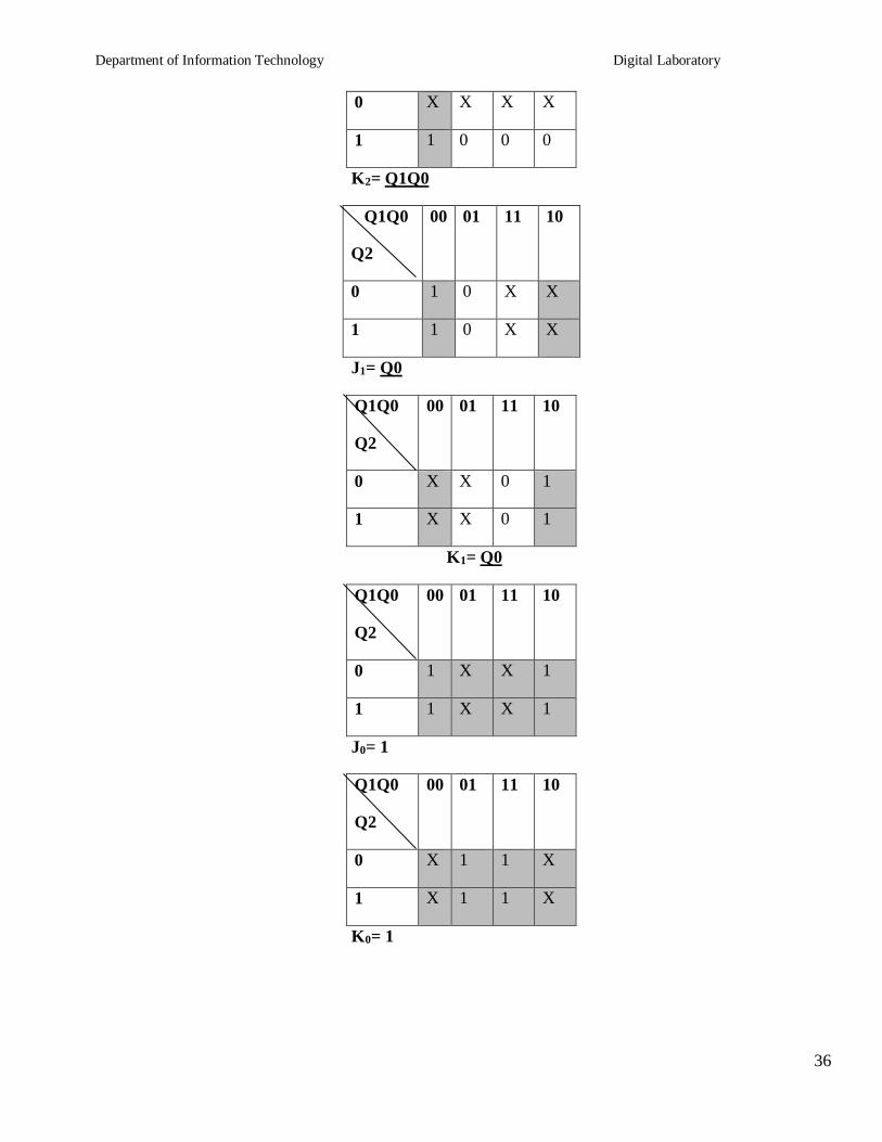
Department of Information Technology Digital Laboratory
42
R9(1)R9(2) These are gated set to nine inputs
QDQCQB Output of internal MOD-5 counter with QD as MSB
QA Output of internal MOD-2 counter with QA as LSB
Input A Clock input to FF-A which is negative edge triggered
Functional Table for IC7490
Reset inputs Output
R0(1) R0(2) R9(0) R9(1) QD QC QB QA
1 1 0 X 0 0 0 0
1 1 X 0 0 0 0 0
X X 1 1 1 0 0 1
X 0 X 0 COUNTER
0 X 0 X COUNTER
0 X X 0 COUNTER
X 0 0 x COUNTER
Department of Information Technology Digital Laboratory
43
Basic internal Structure of IC 7490
Function Table of MOD-5 counter
Design of MOD-10 counter using IC 7490
The QA op the first flip flop is connected to the input B which is clock ip of internal MOD-5 ripple
counter Due to cascading of Mod-2 and Mod-5 counters the overall configuration the decade counters
count from 0000 to 1001 After 1001 mod-5 resets to 0000 and next count after 1001 is 0000
When QA op is connected to B ip we have the Mod-2 counter followed by Mod-5 counter The
count sequence obtained is shown in the table It may be noted that QA changes from 0 to 1 the state of
InputB clock Output
Count QD QC QB
0 0 0 0
0 0 1 1
0 1 0 2
0 1 1 3
1 0 0 4
Department of Information Technology Digital Laboratory
44
Mod-5 counter doesnrsquot change whereas when QA changes from 1 to 0 the Mod-5 counter goes to the next
state
Logic DiagramMOD-10 counter using IC 7490
5 Modulus n Counter
Function table
Ip clock
Output
Count QD QC QB QA
0 0 0 0 0
0 0 0 1 1
0 0 1 0 2
0 0 1 1 3
0 1 0 0 4
Department of Information Technology Digital Laboratory
45
Design of Mod-7 Counter using IC 7490
Mod-7 counter counts through seven states from 0 to 6 counters and it should reset as soon as the
count becomes 7 The op of reset logic should be 1 corresponding to invalid states The reset logic op
should be applied to pin 2 and 3
Truth Table of Reset Logic
0 1 0 1 5
0 1 1 0 6
0 1 1 1 7
1 0 0 0 8
1 0 0 1 9
QD QC QB QA Y
0 0 0 0 0
0 0 0 1 0
0 0 1 0 0
0 0 1 1 0
0 1 0 0 0
0 1 0 1 0
0 1 1 0 0
0 1 1 1 1
1 0 0 0 1
1 0 0 1 1
Department of Information Technology Digital Laboratory
46
Logic Diagram Mod 7 Counter using IC 7490
Function table
Ip clock
Output
Count QD QC QB QA
0 0 0 0 0
0 0 0 1 1
0 0 1 0 2
0 0 1 1 3
0 1 0 0 4
0 1 0 1 5
0 1 1 0 6
Department of Information Technology Digital Laboratory
47
Design of Mod-99 using IC 7490
For Mod-99 two IC 7490rsquos will be required Hence to implement a divide by 99 counter we have
to use two decade counters ICrsquos A divide by 99 counter counts 99 states from 0 to 98 and the counter
should reset as soon as the count becomes 99 So in order to reset the counter of 99 connect the Q op
which are equal to 1 in the count of 99 to an lsquoAndrsquo gate amp then connect and op to the reset ip of both
ICrsquos
MOD-100 Counter-
MOD-100 counter can be obtained by cascading two decade counter ICrsquos
Each IC gives divide by 10 counts Hence 2 ICs will give 1010=100 counts
Clock is applied to the input A of IC 7490 the Q1 output is connected to B input etc
For cascading the QD output of the first IC is connected to the input A of second IC Thus QD of
IC-(1) acts as clock input to IC-(2)
The Ro (1) Ro(2) R9(1) R9(2) inputs of both ICs are connected to ground so as to make them
inactive
The total count provided by the two counters varies from 00 to 99 decimal that means 100 states
Hence it is a MOD-10 counter
Impleacutementations
FigureMOD-100 counters using IC 7490
Department of Information Technology Digital Laboratory
48
B) IC 74191 ndash Theory
IC74191 is 4-bit binary synchronous reversible up down counter It contains 4 master slave flip flops
with internal gating and steering logic to provide asynchronous reset and synchronous count updown
operations its asynchronous parallel capability permits the counter to be preset to any desire number D0
to D3 are the parallel data inputs Information present on the parallel data inputs D0 to D3 is loaded into
the counter and appears on the output when the load PLinput is lowThisoperation overrides the counting
function Counting is inhabited by the high level on the enable G input when G input is low internal state
changes are initiated synchronously by the low to high transitions of the clock inputs the updown input
signal determines the direction of input
Function Table
Operating
mode
Inputs Outputs
PL UD G CLK Dn
Parallel
load L X X X L L
L X X X H H
Count up H L 0 uarr X Count up
Count
down H H 0 uarr X
Count
down
Hold(No
change) H X H X X No change
Pin details ndash
D0 to D3 input lines PL parallel load
G is Enable input ndash enabling the counting
Q0 to Q3 output lines
Downup determines the direction of counting
Clk clock input for counter
Terminal Count Max(1111) min(0000) For these states signal goes high for 1clock pulse
Ripple clock Clock input for next higher state
Department of Information Technology Digital Laboratory
49
Pin Diagram IC 74191
Up counter- Truth Table
Clk
Pulses QA QB QC QD
0 0 0 0 0
1 0 0 0 1
2 0 0 1 0
3 0 0 1 1
4 0 1 0 0
5 0 1 0 1
6 0 1 1 0
7 1 1 1 1
8 1 0 0 0
9 1 0 0 1
10 1 0 1 0
11 1 0 1 1
12 1 1 0 0
13 1 1 0 1
Department of Information Technology Digital Laboratory
50
14 1 1 1 0
15 1 1 1 1
Logic Diagram
Steps-
Connect the circuit as shown above
Apply clock ip to pin no14
Connect UD to GND
Verify the output according to truth table
Logic diagram of down counter
Steps-
Connect the circuit as shown above
Apply clock ip to pin no14
Connect UD to VCC
Verify the output according to truth table
UD D3 D2 D1 D0 PL
Clock IC 74191
G RC
MAX MIN
Q3 Q2 Q1 Q0 TC
vcc
NC
NC
Outputs
no connection
vcc
Department of Information Technology Digital Laboratory
51
With the help of IC74191 we can implement truncated updown counter by using following logic ndash
Connect data input line to particular count you want to load
According to requirement make Truth table
Draw the K-map
Find out Boolean expression
Draw the logic diagram and that is the combinational logic for your count and apply the output of
that circuit to PL
According to requirement we get the UP and down counting
5 Modulus n Counter
Presettable updown counter
Mod 11 counter
Implementation of presetttable mod updown counter using IC- 74LS191
1 Load Data on data lines D0 to D3 (0101)
2 Counter will go through the states from 0101 0110hellip1111 in up counter and 0101 to 0000 in
down counter
Combinational Circuit
CLOCK D3 D2 D1 D0
TC
U D 74191 RC
G PL
Updown Q3 Q2 Q1 Q0 PL
Q3 Q2 Q1 Q0
Preset Count
Department of Information Technology Digital Laboratory
52
3 The logic circuit should be designed in such a way that only when all the outputs are high output
of the reset circuit should be low and the counter should jump to state 5 It should again start
counting from 0101 to 0000
State Table
Down Counter UP Counter
IC 74191 is 4 bit counter Thus it counts 0000 to 1111 different 16 states For MOD11 counter we require
different 11 states so 5 steps must be skipped from 16 states We get MOD11 by presetting counter to
value 5
Assignment Question
Design and Implement MOD 7 MOD 10 and MOD 12 using IC 74191
FAQs
1 What do you mean modulus counter
Counter
state Clock
pulse
Q3 Q2 Q1 Q0
1 0 1 0 1
2 0 1 1 0
3 0 1 1 1
4 1 0 0 0
5 1 0 0 1
6 1 0 1 0
7 1 0 1 1
8 1 1 0 0
9 1 1 0 1
10 1 1 1 1
11 1 1 1 1
Counter state
Clock pulse
FF outputs
Q3 Q2 Q1 Q0
1 0 1 0 1
2 0 1 0 0
3 0 0 1 1
4 0 0 1 0
5 0 0 0 1
6 0 0 0 0
7 0 1 0 1
Department of Information Technology Digital Laboratory
53
It represents the number of possible states of counter
2 How will you use the 7490 IC to design symmetrical divide by 10 frequency counter
The divide by 5 circuit followed by divide by 2 circuit will give symmetrical output
3Where counters are used Give real life example of counter
Modulus n Counter
Binary counter ndash An N stage counter that recycles after 2 Ncount The count proceds in specified binary
sequence Counter Presetable- A counter which can be set to a desired value before the start of the
counting UPDown counter ndash A counter that can count in both up and down direction depending upon a
control input
Department of Information Technology Digital Laboratory
54
Regularity Content Viva-voce Timely
Submission Total
Dated Sign of
Subject
Teacher
2 4 2 2 10
Date of Performance Date of Completion
-------------------------------------------------------------------------------------------------------------------
Assignment No6
------------------------------------------------------------------------------------------------------------------
Title Sequence Generator
------------------------------------------------------------------------------------------------------------------
Objective To understand sequence generator one of the sequential circuit
-------------------------------------------------------------------------------------------------------------------
Problem Statement Design (State Diagram State Table K Map) and implementation of Sequence
Generator using Shift Register IC 74194
-----------------------------------------------------------------------------------------------------------------
Hardware Requirement
i) IC 741947408 (AND-gate) 7432 (OR-gate)
ii) Digital Trainer Kit -1
iii) Patch cords
----------------------------------------------------------------------------------------------------------------
Software Requirement Digital Work 30
------------------------------------------------------------------------------------------------------------------
Theory
Part A Sequence Generator with Flip flop
A sequential circuit which generates a prescribed sequence of bits in synchronism with a clock is referred
to as a sequence generator These pulse trains or sequence of bits can be used to open valves close gates
turn on lights and turn off machines and other variety of jobs
Department of Information Technology Digital Laboratory
55
For the design of sequence generator we first determine the required no of flip flops and the logic circuit
for the next state decoder
No of flip flops required to generate particular sequence can be determined as follows
1) Find the no of 1rsquos in the sequence
2) Find the no of 0rsquos in the sequence
3) Take the maximum out of two
4) If N is the required no of flip flops choose minimum value of lsquonrsquo to satisfy equation given below
Max (0rsquos 1rsquos) le 2n-1
The sequence generator can be classified as
1) sequence generator without bushing
2) sequence generator with bushing
The aim in this experiment is to design a sequence generator to generate a sequence of bit ie 10101
Part B Sequence Generator using Shift Register IC 74194
IC 74194 4 bit bidirectional Shift Register
This bidirectional shift register is designed to incorporate virtually all the features a system designer may
want in a shift register they feature Parallel inputs parallel outputs right shift left shift serialinputs
operating mode control inputsand a direct overriding clear line The register has four distinct modes of
operationsnamely
1 Parallel load
2 Shift right (in the direction QA towards QD)
3 Shift left (in the direction QD towards QA)
4 Inhibit clock (do nothing)
Synchronous parallel loading is accomplished by applying the four bits of data and taking both
mode control inputs S0 and S1High The data is loaded in to the associated flip-flops and appear
at the outputs after positive transition of the clock input During loading serial data flow is
inhibited
Shift right is accomplished synchronously with the rising edge of the clock pulse when S0 is High
and S1 is Low Serial data for this mode is entered at the shift right data input When S0 is Low
and S1 is High data shifts left synchronously and new data is entered at the shift left serial input
Clocking of the flip flop is inhibited when both mode control inputs are LOW
Department of Information Technology Digital Laboratory
56
Mode Control Input Operation
S1 S0
0 0 Clock Inhibit
0 1 Shift right
1 0 Shift Left
1 1 Parallel loading
Function Table of IC 74194
Design
The minimum number of flip-flops N required to generate a sequence of length S is given by S
le 2N ndash 1
In this case S=7 therefore the minimum value of N which may generate in this sequence is 3
However it is not guaranteed to lead to a solution If the given sequence leads to seven distinct
states then only three flip flops are sufficient otherwise we have to increase the number of flip
flops We write the states of circuit as given in table 1 The prescribed sequence is listed under QA
and the sequence listed under QB and QC are the same sequence delayed by one and two clock
pulses respectively From the table we observe that all the states are not distinct which means N=3
is not sufficient Next we assume that N=4 and prepare table 2 The last column gives the required
serial input for getting the desired change of state when a clock pulse is applied This is obtained
by assuming D type flip flop and looking at the QA output For example at the falling edge of first
clock pulse QA=1 The second clock pulse must result in QA=1 which requires its D input to be 1
In the same manner all the entries in column Y are determined
Table 1 State Assignment Table of Sequence Generator (N=3)
Number of Clock
Pulses
Flip Flop Inputs States
QA QB QC
1 1 1 1 7
2 1 1 1 7
3 0 1 1 3
4 1 0 1 5
Department of Information Technology Digital Laboratory
57
5 0 1 0 2
6 1 0 1 5
7 1 1 0 6
Excitation table of D Flip-Flop
Present State Qn Next State Qn+1 Flip-Flop Input D
0 0 0
0 1 1
1 0 0
1 1 1
Table 2State Assignment Table of Sequence Generator (N=4)
Number of Clock
Pulses
Flip Flop Inputs States
Y
Serial ip QA QB QC QD
1 1 1 1 0 14 1
2 1 1 1 1 15 0
3 0 1 1 1 7 1
4 1 0 1 1 11 0
5 0 1 0 1 5 1
6 1 0 1 0 10 1
7 1 1 0 1 13 1
K-Map Simplification
Department of Information Technology Digital Laboratory
58
00 01 11 10
00 X X X X
01 X 1 1 X
11 X 1 0 1
10 X X 0 1
Y= QArsquo + QBrsquo + QCrsquo = QAQBQC
LOGIC DIAGRAM
HARDWARE REQUIREMENTS
Sr no ICs Description Quantity
11 74194 4 bit bidirectional universal shift register 16ktr`
2 7410 3 input NAND Gate 1
Department of Information Technology Digital Laboratory
59
Conclusion In this way sequence generator using JK flip flips amp shift register is designed and
implemented
Enhancements Modifications ndash Sequence generator can also be implemented with shift register instead
of flip flops Use IC 7495 universal shift register IC and try to implement sequence generator
FAQs
1 What is sequential logic circuit
A sequential logic circuit consists of a memory elements in addition to
combinational circuit Its output at any instant of time depends upon
the present input as well as present state of memory element
2 What is meant by delay line
It is used to introduce time delays in digital signals
3 What is meant by following terms
a) Synchronous preset b) Asynchronous preset
c) Synchronous clear d) Asynchronous clear
a)Preset operation is synchronised with the clock
b)Preset operation is independent of the clock
c) clear is performed in synchronous with clock
d) clear is performed independent with clock
4 Is asynchronous counter faster than synchronous counter
In a synchronous counter the time required for change of any state is same and is equal to delay
time of one flip flop where as in asynchronous counter all flip flops are not clocked
simultaneously hence time required is not same
5 What is mean by lockout in counter
In a counter design for a fewer state than the maximum possible state some time it may so happen
that counter enters in unused state and goes from one unused state to another unused state and
never comes to used state
6 What is mean by state table
Department of Information Technology Digital Laboratory
60
It consists of complete information about present state and next state and outputs of a sequential
system
7 What is mean by state diagram
The information available in a state table can be represented as graphically the graphical
representation is known as state diagram
8 What is the advantage of state reduction in the design of sequential circuit
It reduces the number of flip flops
9 What is meant by excitation table
This gives information about what should be the flip flop inputs if outputs are specified before and
after the clock pulse
10 How many flip flops are required to design sequence generator using Counters
max (0rsquoS1rsquoS) in a given sequence lt= 2(N - 1)
Where N = Number of flip flops
11 How many flip flops are required to design sequence generator using shift registers
Slt= 2N - 1
Where N=Number of flip flops
S= Length of sequence
12 What is Lock out condition How it is avoided
When counter enters into one of the invalid state and after application of pulses remains in invalid
states only i e counter gets locked into invalid state amp this is called as lock out Lock out can be
avoided by providing bushing to all the invalid states in such a way that after application of one or
more clock pulses counter will fall into one of the valid state
Department of Information Technology Digital Laboratory
61
Regularity Content Viva-voce Timely
Submission Total
Dated Sign of
Subject
Teacher
2 4 2 2 10
Date of Performance Date of Completion
-------------------------------------------------------------------------------------------------------------------
Assignment No7
------------------------------------------------------------------------------------------------------------------
Title Multiplexer using Data flow modeling and structural modeling
------------------------------------------------------------------------------------------------------------------
Objective To learn data flow modeling style Its uses and different types of declarations with some
different types of circuits Structure of VHDL program is well discussed with this modeling style
-------------------------------------------------------------------------------------------------------------------
Problem Statement 41 multiplexer using data flow amp structural modeling -
----------------------------------------------------------------------------------------------------------------
Hardware Requirement - NA
----------------------------------------------------------------------------------------------------------------
Software Requirement Xilinx
------------------------------------------------------------------------------------------------------------------
Theory
Data flow style-
In this type of design the view of data as flowing from input to output through a design
An operation is defined in terms of a collection of data transformation expressed as concurrent
statement Each of the statement can be activated when any of its input signal changes its value While
these statements describe the behavior of the circuit a lot of information about its structure can be
extracted from the description as well
Data flow modeling has a set of concurrent assignment statements In the data flow level of abstraction we
describe how information is passed in the circuit The built in operators in VHDL are used in expression
such as AND OR XOR NOT etc
Department of Information Technology Digital Laboratory
62
INPUT
Two select lines S1S0
Four data lines D0 D1 D2 D3
OUTPUT
One output line Y
Functional block diagram of 41 Mux
Fig 41 Multiplexer using Data flow modeling
Function table of 41 Mux
Enable S1 S0 A B C D Y
1 X X X X X X 0
0 0 0 A X X X A
0 0 1 X B X X B
0 1 0 X X C X C
0 1 1 X X X D D
Design steps
Click on Xilinx ISE 92i
Create New project from file menu Ensure top level source is HDL
Select family of devices (usually spartan2E or 3)
Department of Information Technology Digital Laboratory
63
Ensure preferred language is VHDL
Click new source which shows you project details device details
and Synthesis and simulator tools
After finishing project create new source by right clicking in project name with VHDL
module
Complete ports name directions and bus Ensure architecture name is behavioral
After that we will get design summary and detailed reports
Close design summary
Create your code with given modeling style
Go to process window and synthesis to check if any error is there in code Check syntax and
view RTL schematic
Create new source to simulate the code
Right click on source name and create test bench waveform with proper name Ensure the
project is same
Click on combinational circuit in initial timing wizard
Select test bench wave in source window Apply inputs to wave diagram Ensure you are in
behavioral simulation
Go to process box Click on Xilinx ISE simulator and simulate the model See results
RTL Schematic
Department of Information Technology Digital Laboratory
64
Timing Diagram
FAQrsquos
1 What are the different kinds of data objects in VHDL code
Ans data object may be any value or number still some signal data objects and bit and bit_vector
types of these are available in VHDL STD_LOGIC and STD_LOGIC_VECTOR types are used
widely in programming
2 What do you mean by signal
Ans signal is a data object represents logic signals or wires in a circuit There are three places in
which signals can be declared in VHDL code in an entity declaration in the declarative section of
architecture and in declarative section of package
3 What are different signal types
Ans BIT BIT_VECTOR STD_LOGIC STD_LOGIC_VECTOR STD_ULOGIC SIGNED
UNSIGNED INTEGER ENUMERATION and BOOLEAN
4 What is an entity
Ans a circuit or sub circuit described with VHDL code is called a design entity
5 Explain structure of an entity
Ans it has two main parts the entity declaration which specifies the input and output signals for
entity and the architecture which gives circuit details
Department of Information Technology Digital Laboratory
65
6 How will you declare a package with component Explain structure
The general form of package declaration is as shown in diagram
PACKAGE package_name IS
[TYPE declarations]
[SIGNAL declarations]
[COMPONENT declarations]
END package_name
Entity
Declaration Architecture
Department of Information Technology Digital Laboratory
66
Regularity Content Viva-voce Timely
Submission Total
Dated Sign of
Subject
Teacher
2 4 2 2 10
Date of Performance Date of Completion
-------------------------------------------------------------------------------------------------------------------
Assignment No8
------------------------------------------------------------------------------------------------------------------
Title Full Adder using Behavioral and Structural modeling
------------------------------------------------------------------------------------------------------------------
Objective To learn structural modeling style Its uses and different types of declarations with some
different types of circuits Structure of VHDL program is well discussed with this modeling style
-------------------------------------------------------------------------------------------------------------------
Problem Statement Full adder using behavioral amp structural modeling
-----------------------------------------------------------------------------------------------------------------
Hardware Requirement - NA
----------------------------------------------------------------------------------------------------------------
Software Requirement Xilinx
------------------------------------------------------------------------------------------------------------------
Theory
Structural style-
A digital electronic system can be described as a module with inputs andor outputs The electrical values
on the outputs are same functions of the values of inputs The example of it is as shown The NAND gate
has 2ips AampB amp an output y Using VHDL terminology we call the NAND2 design entity amp the inputs
amp outputs are called ports 1 way of describing the function of NAND2 is to describe how it is composed
of sub modules AND amp INVERTER Each of the Sub modules is an instance of some entity amp ports of the
instances are connected using signals Structural modeling has a set of interconnected component
Structure can be used to create a very low level description of a circuit or a very high level description
Department of Information Technology Digital Laboratory
67
In a gate level description of a circuit for example components such as basic logic gates amp FFs might be
connected in some logical stricture to create the circuit This is what is often called a net list
Structure of structural modeling
Functional block diagram of Full Adder
architectureNetlistofHalf_Adderis
-- component with locals
componentMyXorport (A_XorB_Xor in BIT
Z_Xor out BIT)
end component
-- component with locals
componentMyAndport (A_AndB_And in BIT
Z_And out BIT)
end component
begin
Xor1 MyXorport map (X Y Sum)
-- instance with actuals
And1 MyAndport map (X Y Cout)
-- instance with actuals
end
Department of Information Technology Digital Laboratory
68
Function table of Full Adder
A B Cin SUM CARRY
0 0 0 0 0
0 0 1 1 0
0 1 0 1 0
0 1 1 0 1
1 0 0 1 0
1 0 1 0 1
1 1 0 0 1
1 1 1 1 1
Sum = Σm(1 2 4 7)
Carry= Σm(3 5 6 7)
Design steps
Click on Xilinx ISE 92i
Create New project from file menu Ensure top level source is HDL
Select family of devices (usually spartan2E or 3)
Ensure preferred language is VHDL
Click new source which shows you project details device details
and Synthesis and simulator tools
After finishing project create new source(full adder) by right clicking in project name with
VHDL module
Complete ports name directions and bus Ensure architecture name is behavioral
After that we will get design summary and detailed reports
Close design summary
Click new source which shows you project details device details
and Synthesis and simulator tools
After finishing project create new source(half adder) by right clicking in project name with
VHDL module
Complete ports name directions and bus Ensure architecture name is behavioral Names
should be same as previous inputs
Department of Information Technology Digital Laboratory
69
After that we will get design summary and detailed reports
Close design summary
Create your code for half adder with given modeling style
After that go to process window Click on design utilities
View HDL instantiation code of half adder
Copy component part of half adder in architecture block of full adder Copy instantiation
template twice after begin as we require two half adders to construct full adder (structural
modeling) Name them differently (eg ha1 or ha2)
Create signals as per the logic Complete code of full adder
Go to process window and synthesis to check if any error is there in code Check syntax and
view RTL schematic
Create new source to simulate the code
Right click on source name and create test bench waveform with proper name Ensure the
project is same
Click on combinational circuit in initial timing wizard
Select test bench wave in source window Apply inputs to wave diagram Ensure you are in
behavioral simulation
Go to process box Click on Xilinx ISE simulator and simulate the model See results
RTL Schematic
Timing Diagram
Department of Information Technology Digital Laboratory
70
INPUT
Three inputs A B Carry (previous)
OUTPUT
Two outputs Sum Carry
FAQrsquos
1 What do you mean by structural style
Ans in this type of code a circuit is described in hierarchical fashion by connecting together sub
circuits
2 Explain IF statement with example
Ans The general form of an IF statement is as follws
IF Sel=rsquo0rsquo THEN
Flt=x1
ELSE
Flt=x2
END IF
Department of Information Technology Digital Laboratory
71
3 Explain declaration and instantiation process in VHDL
Ans first declare a small vhdl code in formal way Eg half adder Define project name is full adder
And simply copy instantiation template in main source code Define how many times you want to
declare this template Give separate names for those
4 What is STD_LOGIC_VECTOR
Ans It is standard data object added to VHDL standard in IEEE 1164 It provides more flexibility
than the Bit type
5 Explain difference between concurrent and sequential statements
Ans Concurrent statements define interconnected processes and blocks that together describe a designrsquos
overall behavior or structure They can be grouped using block sstatement Groups of blocks can also be
partitioned into other blocks At this same level a VHDL component can be connected to define signals
within the blocks
It is a reference to an entity A process can be a single signal assignment statement or a series of
sequential statements (SS) Within a process procedures and functions can partition the sequential
statements
PRACTICE ASSIGNMENTS
1 Implement half adder using data flow modeling
2 Implement Full Adder using behavioral modeling
3 Implement 3 bit magnitude comparator using a 3 bit adder
4 Implement half sub tractor using data flow modeling
5 Write VHDL code for Full Subtractor
Department of Information Technology Digital Laboratory
72
Regularity Content Viva-voce Timely
Submission Total
Dated Sign of
Subject
Teacher
2 4 2 2 10
rsquozaDate of Performance Date of Completion
-------------------------------------------------------------------------------------------------------------------
Assignment No9
------------------------------------------------------------------------------------------------------------------
Title Simulation of 3 bit Connter using Behavioral modeling
------------------------------------------------------------------------------------------------------------------
Objective To learn behavioral modeling style Its uses and different types of declarations with some
different types of circuits Structure of VHDL program is well discussed with this modeling style
-------------------------------------------------------------------------------------------------------------------
Problem Statement 3 bit controlled up down synchronous counter with preset amp clear
-----------------------------------------------------------------------------------------------------------------
Hardware Requirement -NA
----------------------------------------------------------------------------------------------------------------
Software Requirement Xilinx
------------------------------------------------------------------------------------------------------------------
Theory
Behavioral style-
Highest level of abstraction supported in VHDL is called the behavior level of abstraction In it we have
for loop while loop If then else case ampvariable assignment The statements are enclosed in a PROCESS
block amp are executed sequentially
In it circuit is described in terms of its operation overtime
In behavioral description the concept of time may be expressed precisely with actual delays between
related events (such as the propagation delays within gates amp on wires) or it may be simply an ordering of
operation that are expressed sequentially (such as in a functional description of a FF)
Department of Information Technology Digital Laboratory
73
A behavioral design method defines a circuit in terms of text language rather than a schematic of
interconnected symbols
Behavioral design is a technology independent text based design that incorporates high level
functionality amp high level information flow
Structure of Behavioral modeling
Functional block diagram of 3 bit controlled up down synchronous counter with preset amp clear
Function table of 3 bit controlled up down synchronous counter with preset amp clear
Design steps
Click on Xilinx ISE 92i
Create New project from file menu Ensure top level source is HDL
Select family of devices (usually spartan2E or 3)
Ensure preferred language is VHDL
Click new source which shows you project details device details
and Synthesis and simulator tools
After finishing project create new source by right clicking in project name with VHDL
module
Complete ports name directions and bus Ensure architecture name is behavioral
After that we will get design summary and detailed reports
Close design summary
Create your code with given modeling style
Go to process window and synthesis to check if any error is there in code Check syntax
and view RTL schematic Create new source to simulate the code
Department of Information Technology Digital Laboratory
74
Right click on source name and create test bench waveform with proper name Ensure the
project is same
Click on combinational circuit in initial timing wizard
Select test bench wave in source window Apply inputs to wave diagram Ensure you are in
behavioral simulation
Go to process box Click on Xilinx ISE simulator and simulate the model
RTL Schematic
Timing Diagram
INPUT
Clock Preset Clear
OUTPUT
Three output lines
FAQrsquos
1 Explain the structure of behavioral modeling
2 What are the differences between behavioral and structural modeling
Ans Behavioral descriptionof a circuit is the highest level of abstraction in VHDL Here the
circuit is described in terms of it operation with respect to time All operations are in one level of
code The operations are described in a way that the designer of a sequential circuit infers a
register
Structural description on the other hand is a circuit description in terms of its components
it can either create a low level description much like a hierarchy in a block diagram Whenever
you see a component instantiated in a code that code employs structural description of the circuit
The components are connected in the form of a netlist This is for better manageability and
reusability
3 What are the differences between behavioral and data flow modeling
Department of Information Technology Digital Laboratory
75
Ans Behavioral ndash describes how the output is derived from the inputs using structured
statements
Dataflow ndash describes how the data flows from the inputs to the output most often
using NOT AND and OR operations
4 What do you mean by process statement
Ans The process statement begins with the PROCESS keyword followed by a parenthesized list
of signals called the sensitivity list It operates on selected and conditional statements
5 Explain syntax of process statement
Ans BEGIN
Process( sensitivity list)
END process
PRACTICE ASSIGNMENTS
1 Implement 3 bit asynchronous up counter using behavioral modeling
2 Implement 3 bit asynchronous down counter using behavioral modeling
3 Implement 3 bit synchronous down counter using behavioral modeling
End
Department of Information Technology Digital Laboratory
76
Pin Diagrams
7400 Quad 2-Input NAND Gate
7402 Quad 2-Input NOR Gate
7404 Not Gates
7408 Quad 2-Input AND Gates
7432 Quad 2-Input OR Gate
7486 Quad 2-Input Exclusive-OR Gate
Department of Information Technology Digital Laboratory
77
7483 4 bit Binary Adder
7490 Decade and Binary Counters
74138 38 Decoder
Department of Information Technology Digital Laboratory
78
74153 Dual 41 Multiplexer
74191 Synchronous UpDown 4 bit Binary counter with Mode Control
Department of Information Technology Digital Laboratory
79
74194 Universal Shift Register
7476 Dual Master-Slave J-K Flip-Flops
- Part B Sequence Generator using Shift Register IC 74194
-
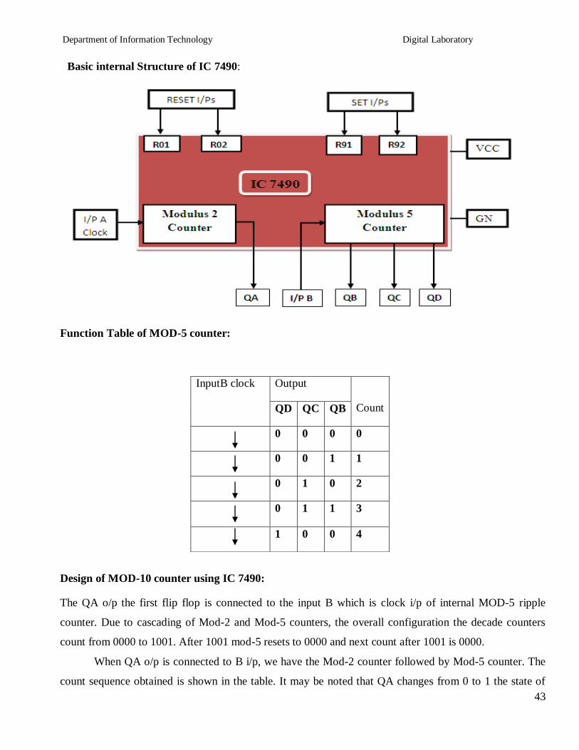
Department of Information Technology Digital Laboratory
46
Logic Diagram Mod 7 Counter using IC 7490
Function table
Ip clock
Output
Count QD QC QB QA
0 0 0 0 0
0 0 0 1 1
0 0 1 0 2
0 0 1 1 3
0 1 0 0 4
0 1 0 1 5
0 1 1 0 6
Department of Information Technology Digital Laboratory
47
Design of Mod-99 using IC 7490
For Mod-99 two IC 7490rsquos will be required Hence to implement a divide by 99 counter we have
to use two decade counters ICrsquos A divide by 99 counter counts 99 states from 0 to 98 and the counter
should reset as soon as the count becomes 99 So in order to reset the counter of 99 connect the Q op
which are equal to 1 in the count of 99 to an lsquoAndrsquo gate amp then connect and op to the reset ip of both
ICrsquos
MOD-100 Counter-
MOD-100 counter can be obtained by cascading two decade counter ICrsquos
Each IC gives divide by 10 counts Hence 2 ICs will give 1010=100 counts
Clock is applied to the input A of IC 7490 the Q1 output is connected to B input etc
For cascading the QD output of the first IC is connected to the input A of second IC Thus QD of
IC-(1) acts as clock input to IC-(2)
The Ro (1) Ro(2) R9(1) R9(2) inputs of both ICs are connected to ground so as to make them
inactive
The total count provided by the two counters varies from 00 to 99 decimal that means 100 states
Hence it is a MOD-10 counter
Impleacutementations
FigureMOD-100 counters using IC 7490
Department of Information Technology Digital Laboratory
48
B) IC 74191 ndash Theory
IC74191 is 4-bit binary synchronous reversible up down counter It contains 4 master slave flip flops
with internal gating and steering logic to provide asynchronous reset and synchronous count updown
operations its asynchronous parallel capability permits the counter to be preset to any desire number D0
to D3 are the parallel data inputs Information present on the parallel data inputs D0 to D3 is loaded into
the counter and appears on the output when the load PLinput is lowThisoperation overrides the counting
function Counting is inhabited by the high level on the enable G input when G input is low internal state
changes are initiated synchronously by the low to high transitions of the clock inputs the updown input
signal determines the direction of input
Function Table
Operating
mode
Inputs Outputs
PL UD G CLK Dn
Parallel
load L X X X L L
L X X X H H
Count up H L 0 uarr X Count up
Count
down H H 0 uarr X
Count
down
Hold(No
change) H X H X X No change
Pin details ndash
D0 to D3 input lines PL parallel load
G is Enable input ndash enabling the counting
Q0 to Q3 output lines
Downup determines the direction of counting
Clk clock input for counter
Terminal Count Max(1111) min(0000) For these states signal goes high for 1clock pulse
Ripple clock Clock input for next higher state
Department of Information Technology Digital Laboratory
49
Pin Diagram IC 74191
Up counter- Truth Table
Clk
Pulses QA QB QC QD
0 0 0 0 0
1 0 0 0 1
2 0 0 1 0
3 0 0 1 1
4 0 1 0 0
5 0 1 0 1
6 0 1 1 0
7 1 1 1 1
8 1 0 0 0
9 1 0 0 1
10 1 0 1 0
11 1 0 1 1
12 1 1 0 0
13 1 1 0 1
Department of Information Technology Digital Laboratory
50
14 1 1 1 0
15 1 1 1 1
Logic Diagram
Steps-
Connect the circuit as shown above
Apply clock ip to pin no14
Connect UD to GND
Verify the output according to truth table
Logic diagram of down counter
Steps-
Connect the circuit as shown above
Apply clock ip to pin no14
Connect UD to VCC
Verify the output according to truth table
UD D3 D2 D1 D0 PL
Clock IC 74191
G RC
MAX MIN
Q3 Q2 Q1 Q0 TC
vcc
NC
NC
Outputs
no connection
vcc
Department of Information Technology Digital Laboratory
51
With the help of IC74191 we can implement truncated updown counter by using following logic ndash
Connect data input line to particular count you want to load
According to requirement make Truth table
Draw the K-map
Find out Boolean expression
Draw the logic diagram and that is the combinational logic for your count and apply the output of
that circuit to PL
According to requirement we get the UP and down counting
5 Modulus n Counter
Presettable updown counter
Mod 11 counter
Implementation of presetttable mod updown counter using IC- 74LS191
1 Load Data on data lines D0 to D3 (0101)
2 Counter will go through the states from 0101 0110hellip1111 in up counter and 0101 to 0000 in
down counter
Combinational Circuit
CLOCK D3 D2 D1 D0
TC
U D 74191 RC
G PL
Updown Q3 Q2 Q1 Q0 PL
Q3 Q2 Q1 Q0
Preset Count
Department of Information Technology Digital Laboratory
52
3 The logic circuit should be designed in such a way that only when all the outputs are high output
of the reset circuit should be low and the counter should jump to state 5 It should again start
counting from 0101 to 0000
State Table
Down Counter UP Counter
IC 74191 is 4 bit counter Thus it counts 0000 to 1111 different 16 states For MOD11 counter we require
different 11 states so 5 steps must be skipped from 16 states We get MOD11 by presetting counter to
value 5
Assignment Question
Design and Implement MOD 7 MOD 10 and MOD 12 using IC 74191
FAQs
1 What do you mean modulus counter
Counter
state Clock
pulse
Q3 Q2 Q1 Q0
1 0 1 0 1
2 0 1 1 0
3 0 1 1 1
4 1 0 0 0
5 1 0 0 1
6 1 0 1 0
7 1 0 1 1
8 1 1 0 0
9 1 1 0 1
10 1 1 1 1
11 1 1 1 1
Counter state
Clock pulse
FF outputs
Q3 Q2 Q1 Q0
1 0 1 0 1
2 0 1 0 0
3 0 0 1 1
4 0 0 1 0
5 0 0 0 1
6 0 0 0 0
7 0 1 0 1
Department of Information Technology Digital Laboratory
53
It represents the number of possible states of counter
2 How will you use the 7490 IC to design symmetrical divide by 10 frequency counter
The divide by 5 circuit followed by divide by 2 circuit will give symmetrical output
3Where counters are used Give real life example of counter
Modulus n Counter
Binary counter ndash An N stage counter that recycles after 2 Ncount The count proceds in specified binary
sequence Counter Presetable- A counter which can be set to a desired value before the start of the
counting UPDown counter ndash A counter that can count in both up and down direction depending upon a
control input
Department of Information Technology Digital Laboratory
54
Regularity Content Viva-voce Timely
Submission Total
Dated Sign of
Subject
Teacher
2 4 2 2 10
Date of Performance Date of Completion
-------------------------------------------------------------------------------------------------------------------
Assignment No6
------------------------------------------------------------------------------------------------------------------
Title Sequence Generator
------------------------------------------------------------------------------------------------------------------
Objective To understand sequence generator one of the sequential circuit
-------------------------------------------------------------------------------------------------------------------
Problem Statement Design (State Diagram State Table K Map) and implementation of Sequence
Generator using Shift Register IC 74194
-----------------------------------------------------------------------------------------------------------------
Hardware Requirement
i) IC 741947408 (AND-gate) 7432 (OR-gate)
ii) Digital Trainer Kit -1
iii) Patch cords
----------------------------------------------------------------------------------------------------------------
Software Requirement Digital Work 30
------------------------------------------------------------------------------------------------------------------
Theory
Part A Sequence Generator with Flip flop
A sequential circuit which generates a prescribed sequence of bits in synchronism with a clock is referred
to as a sequence generator These pulse trains or sequence of bits can be used to open valves close gates
turn on lights and turn off machines and other variety of jobs
Department of Information Technology Digital Laboratory
55
For the design of sequence generator we first determine the required no of flip flops and the logic circuit
for the next state decoder
No of flip flops required to generate particular sequence can be determined as follows
1) Find the no of 1rsquos in the sequence
2) Find the no of 0rsquos in the sequence
3) Take the maximum out of two
4) If N is the required no of flip flops choose minimum value of lsquonrsquo to satisfy equation given below
Max (0rsquos 1rsquos) le 2n-1
The sequence generator can be classified as
1) sequence generator without bushing
2) sequence generator with bushing
The aim in this experiment is to design a sequence generator to generate a sequence of bit ie 10101
Part B Sequence Generator using Shift Register IC 74194
IC 74194 4 bit bidirectional Shift Register
This bidirectional shift register is designed to incorporate virtually all the features a system designer may
want in a shift register they feature Parallel inputs parallel outputs right shift left shift serialinputs
operating mode control inputsand a direct overriding clear line The register has four distinct modes of
operationsnamely
1 Parallel load
2 Shift right (in the direction QA towards QD)
3 Shift left (in the direction QD towards QA)
4 Inhibit clock (do nothing)
Synchronous parallel loading is accomplished by applying the four bits of data and taking both
mode control inputs S0 and S1High The data is loaded in to the associated flip-flops and appear
at the outputs after positive transition of the clock input During loading serial data flow is
inhibited
Shift right is accomplished synchronously with the rising edge of the clock pulse when S0 is High
and S1 is Low Serial data for this mode is entered at the shift right data input When S0 is Low
and S1 is High data shifts left synchronously and new data is entered at the shift left serial input
Clocking of the flip flop is inhibited when both mode control inputs are LOW
Department of Information Technology Digital Laboratory
56
Mode Control Input Operation
S1 S0
0 0 Clock Inhibit
0 1 Shift right
1 0 Shift Left
1 1 Parallel loading
Function Table of IC 74194
Design
The minimum number of flip-flops N required to generate a sequence of length S is given by S
le 2N ndash 1
In this case S=7 therefore the minimum value of N which may generate in this sequence is 3
However it is not guaranteed to lead to a solution If the given sequence leads to seven distinct
states then only three flip flops are sufficient otherwise we have to increase the number of flip
flops We write the states of circuit as given in table 1 The prescribed sequence is listed under QA
and the sequence listed under QB and QC are the same sequence delayed by one and two clock
pulses respectively From the table we observe that all the states are not distinct which means N=3
is not sufficient Next we assume that N=4 and prepare table 2 The last column gives the required
serial input for getting the desired change of state when a clock pulse is applied This is obtained
by assuming D type flip flop and looking at the QA output For example at the falling edge of first
clock pulse QA=1 The second clock pulse must result in QA=1 which requires its D input to be 1
In the same manner all the entries in column Y are determined
Table 1 State Assignment Table of Sequence Generator (N=3)
Number of Clock
Pulses
Flip Flop Inputs States
QA QB QC
1 1 1 1 7
2 1 1 1 7
3 0 1 1 3
4 1 0 1 5
Department of Information Technology Digital Laboratory
57
5 0 1 0 2
6 1 0 1 5
7 1 1 0 6
Excitation table of D Flip-Flop
Present State Qn Next State Qn+1 Flip-Flop Input D
0 0 0
0 1 1
1 0 0
1 1 1
Table 2State Assignment Table of Sequence Generator (N=4)
Number of Clock
Pulses
Flip Flop Inputs States
Y
Serial ip QA QB QC QD
1 1 1 1 0 14 1
2 1 1 1 1 15 0
3 0 1 1 1 7 1
4 1 0 1 1 11 0
5 0 1 0 1 5 1
6 1 0 1 0 10 1
7 1 1 0 1 13 1
K-Map Simplification
Department of Information Technology Digital Laboratory
58
00 01 11 10
00 X X X X
01 X 1 1 X
11 X 1 0 1
10 X X 0 1
Y= QArsquo + QBrsquo + QCrsquo = QAQBQC
LOGIC DIAGRAM
HARDWARE REQUIREMENTS
Sr no ICs Description Quantity
11 74194 4 bit bidirectional universal shift register 16ktr`
2 7410 3 input NAND Gate 1
Department of Information Technology Digital Laboratory
59
Conclusion In this way sequence generator using JK flip flips amp shift register is designed and
implemented
Enhancements Modifications ndash Sequence generator can also be implemented with shift register instead
of flip flops Use IC 7495 universal shift register IC and try to implement sequence generator
FAQs
1 What is sequential logic circuit
A sequential logic circuit consists of a memory elements in addition to
combinational circuit Its output at any instant of time depends upon
the present input as well as present state of memory element
2 What is meant by delay line
It is used to introduce time delays in digital signals
3 What is meant by following terms
a) Synchronous preset b) Asynchronous preset
c) Synchronous clear d) Asynchronous clear
a)Preset operation is synchronised with the clock
b)Preset operation is independent of the clock
c) clear is performed in synchronous with clock
d) clear is performed independent with clock
4 Is asynchronous counter faster than synchronous counter
In a synchronous counter the time required for change of any state is same and is equal to delay
time of one flip flop where as in asynchronous counter all flip flops are not clocked
simultaneously hence time required is not same
5 What is mean by lockout in counter
In a counter design for a fewer state than the maximum possible state some time it may so happen
that counter enters in unused state and goes from one unused state to another unused state and
never comes to used state
6 What is mean by state table
Department of Information Technology Digital Laboratory
60
It consists of complete information about present state and next state and outputs of a sequential
system
7 What is mean by state diagram
The information available in a state table can be represented as graphically the graphical
representation is known as state diagram
8 What is the advantage of state reduction in the design of sequential circuit
It reduces the number of flip flops
9 What is meant by excitation table
This gives information about what should be the flip flop inputs if outputs are specified before and
after the clock pulse
10 How many flip flops are required to design sequence generator using Counters
max (0rsquoS1rsquoS) in a given sequence lt= 2(N - 1)
Where N = Number of flip flops
11 How many flip flops are required to design sequence generator using shift registers
Slt= 2N - 1
Where N=Number of flip flops
S= Length of sequence
12 What is Lock out condition How it is avoided
When counter enters into one of the invalid state and after application of pulses remains in invalid
states only i e counter gets locked into invalid state amp this is called as lock out Lock out can be
avoided by providing bushing to all the invalid states in such a way that after application of one or
more clock pulses counter will fall into one of the valid state
Department of Information Technology Digital Laboratory
61
Regularity Content Viva-voce Timely
Submission Total
Dated Sign of
Subject
Teacher
2 4 2 2 10
Date of Performance Date of Completion
-------------------------------------------------------------------------------------------------------------------
Assignment No7
------------------------------------------------------------------------------------------------------------------
Title Multiplexer using Data flow modeling and structural modeling
------------------------------------------------------------------------------------------------------------------
Objective To learn data flow modeling style Its uses and different types of declarations with some
different types of circuits Structure of VHDL program is well discussed with this modeling style
-------------------------------------------------------------------------------------------------------------------
Problem Statement 41 multiplexer using data flow amp structural modeling -
----------------------------------------------------------------------------------------------------------------
Hardware Requirement - NA
----------------------------------------------------------------------------------------------------------------
Software Requirement Xilinx
------------------------------------------------------------------------------------------------------------------
Theory
Data flow style-
In this type of design the view of data as flowing from input to output through a design
An operation is defined in terms of a collection of data transformation expressed as concurrent
statement Each of the statement can be activated when any of its input signal changes its value While
these statements describe the behavior of the circuit a lot of information about its structure can be
extracted from the description as well
Data flow modeling has a set of concurrent assignment statements In the data flow level of abstraction we
describe how information is passed in the circuit The built in operators in VHDL are used in expression
such as AND OR XOR NOT etc
Department of Information Technology Digital Laboratory
62
INPUT
Two select lines S1S0
Four data lines D0 D1 D2 D3
OUTPUT
One output line Y
Functional block diagram of 41 Mux
Fig 41 Multiplexer using Data flow modeling
Function table of 41 Mux
Enable S1 S0 A B C D Y
1 X X X X X X 0
0 0 0 A X X X A
0 0 1 X B X X B
0 1 0 X X C X C
0 1 1 X X X D D
Design steps
Click on Xilinx ISE 92i
Create New project from file menu Ensure top level source is HDL
Select family of devices (usually spartan2E or 3)
Department of Information Technology Digital Laboratory
63
Ensure preferred language is VHDL
Click new source which shows you project details device details
and Synthesis and simulator tools
After finishing project create new source by right clicking in project name with VHDL
module
Complete ports name directions and bus Ensure architecture name is behavioral
After that we will get design summary and detailed reports
Close design summary
Create your code with given modeling style
Go to process window and synthesis to check if any error is there in code Check syntax and
view RTL schematic
Create new source to simulate the code
Right click on source name and create test bench waveform with proper name Ensure the
project is same
Click on combinational circuit in initial timing wizard
Select test bench wave in source window Apply inputs to wave diagram Ensure you are in
behavioral simulation
Go to process box Click on Xilinx ISE simulator and simulate the model See results
RTL Schematic
Department of Information Technology Digital Laboratory
64
Timing Diagram
FAQrsquos
1 What are the different kinds of data objects in VHDL code
Ans data object may be any value or number still some signal data objects and bit and bit_vector
types of these are available in VHDL STD_LOGIC and STD_LOGIC_VECTOR types are used
widely in programming
2 What do you mean by signal
Ans signal is a data object represents logic signals or wires in a circuit There are three places in
which signals can be declared in VHDL code in an entity declaration in the declarative section of
architecture and in declarative section of package
3 What are different signal types
Ans BIT BIT_VECTOR STD_LOGIC STD_LOGIC_VECTOR STD_ULOGIC SIGNED
UNSIGNED INTEGER ENUMERATION and BOOLEAN
4 What is an entity
Ans a circuit or sub circuit described with VHDL code is called a design entity
5 Explain structure of an entity
Ans it has two main parts the entity declaration which specifies the input and output signals for
entity and the architecture which gives circuit details
Department of Information Technology Digital Laboratory
65
6 How will you declare a package with component Explain structure
The general form of package declaration is as shown in diagram
PACKAGE package_name IS
[TYPE declarations]
[SIGNAL declarations]
[COMPONENT declarations]
END package_name
Entity
Declaration Architecture
Department of Information Technology Digital Laboratory
66
Regularity Content Viva-voce Timely
Submission Total
Dated Sign of
Subject
Teacher
2 4 2 2 10
Date of Performance Date of Completion
-------------------------------------------------------------------------------------------------------------------
Assignment No8
------------------------------------------------------------------------------------------------------------------
Title Full Adder using Behavioral and Structural modeling
------------------------------------------------------------------------------------------------------------------
Objective To learn structural modeling style Its uses and different types of declarations with some
different types of circuits Structure of VHDL program is well discussed with this modeling style
-------------------------------------------------------------------------------------------------------------------
Problem Statement Full adder using behavioral amp structural modeling
-----------------------------------------------------------------------------------------------------------------
Hardware Requirement - NA
----------------------------------------------------------------------------------------------------------------
Software Requirement Xilinx
------------------------------------------------------------------------------------------------------------------
Theory
Structural style-
A digital electronic system can be described as a module with inputs andor outputs The electrical values
on the outputs are same functions of the values of inputs The example of it is as shown The NAND gate
has 2ips AampB amp an output y Using VHDL terminology we call the NAND2 design entity amp the inputs
amp outputs are called ports 1 way of describing the function of NAND2 is to describe how it is composed
of sub modules AND amp INVERTER Each of the Sub modules is an instance of some entity amp ports of the
instances are connected using signals Structural modeling has a set of interconnected component
Structure can be used to create a very low level description of a circuit or a very high level description
Department of Information Technology Digital Laboratory
67
In a gate level description of a circuit for example components such as basic logic gates amp FFs might be
connected in some logical stricture to create the circuit This is what is often called a net list
Structure of structural modeling
Functional block diagram of Full Adder
architectureNetlistofHalf_Adderis
-- component with locals
componentMyXorport (A_XorB_Xor in BIT
Z_Xor out BIT)
end component
-- component with locals
componentMyAndport (A_AndB_And in BIT
Z_And out BIT)
end component
begin
Xor1 MyXorport map (X Y Sum)
-- instance with actuals
And1 MyAndport map (X Y Cout)
-- instance with actuals
end
Department of Information Technology Digital Laboratory
68
Function table of Full Adder
A B Cin SUM CARRY
0 0 0 0 0
0 0 1 1 0
0 1 0 1 0
0 1 1 0 1
1 0 0 1 0
1 0 1 0 1
1 1 0 0 1
1 1 1 1 1
Sum = Σm(1 2 4 7)
Carry= Σm(3 5 6 7)
Design steps
Click on Xilinx ISE 92i
Create New project from file menu Ensure top level source is HDL
Select family of devices (usually spartan2E or 3)
Ensure preferred language is VHDL
Click new source which shows you project details device details
and Synthesis and simulator tools
After finishing project create new source(full adder) by right clicking in project name with
VHDL module
Complete ports name directions and bus Ensure architecture name is behavioral
After that we will get design summary and detailed reports
Close design summary
Click new source which shows you project details device details
and Synthesis and simulator tools
After finishing project create new source(half adder) by right clicking in project name with
VHDL module
Complete ports name directions and bus Ensure architecture name is behavioral Names
should be same as previous inputs
Department of Information Technology Digital Laboratory
69
After that we will get design summary and detailed reports
Close design summary
Create your code for half adder with given modeling style
After that go to process window Click on design utilities
View HDL instantiation code of half adder
Copy component part of half adder in architecture block of full adder Copy instantiation
template twice after begin as we require two half adders to construct full adder (structural
modeling) Name them differently (eg ha1 or ha2)
Create signals as per the logic Complete code of full adder
Go to process window and synthesis to check if any error is there in code Check syntax and
view RTL schematic
Create new source to simulate the code
Right click on source name and create test bench waveform with proper name Ensure the
project is same
Click on combinational circuit in initial timing wizard
Select test bench wave in source window Apply inputs to wave diagram Ensure you are in
behavioral simulation
Go to process box Click on Xilinx ISE simulator and simulate the model See results
RTL Schematic
Timing Diagram
Department of Information Technology Digital Laboratory
70
INPUT
Three inputs A B Carry (previous)
OUTPUT
Two outputs Sum Carry
FAQrsquos
1 What do you mean by structural style
Ans in this type of code a circuit is described in hierarchical fashion by connecting together sub
circuits
2 Explain IF statement with example
Ans The general form of an IF statement is as follws
IF Sel=rsquo0rsquo THEN
Flt=x1
ELSE
Flt=x2
END IF
Department of Information Technology Digital Laboratory
71
3 Explain declaration and instantiation process in VHDL
Ans first declare a small vhdl code in formal way Eg half adder Define project name is full adder
And simply copy instantiation template in main source code Define how many times you want to
declare this template Give separate names for those
4 What is STD_LOGIC_VECTOR
Ans It is standard data object added to VHDL standard in IEEE 1164 It provides more flexibility
than the Bit type
5 Explain difference between concurrent and sequential statements
Ans Concurrent statements define interconnected processes and blocks that together describe a designrsquos
overall behavior or structure They can be grouped using block sstatement Groups of blocks can also be
partitioned into other blocks At this same level a VHDL component can be connected to define signals
within the blocks
It is a reference to an entity A process can be a single signal assignment statement or a series of
sequential statements (SS) Within a process procedures and functions can partition the sequential
statements
PRACTICE ASSIGNMENTS
1 Implement half adder using data flow modeling
2 Implement Full Adder using behavioral modeling
3 Implement 3 bit magnitude comparator using a 3 bit adder
4 Implement half sub tractor using data flow modeling
5 Write VHDL code for Full Subtractor
Department of Information Technology Digital Laboratory
72
Regularity Content Viva-voce Timely
Submission Total
Dated Sign of
Subject
Teacher
2 4 2 2 10
rsquozaDate of Performance Date of Completion
-------------------------------------------------------------------------------------------------------------------
Assignment No9
------------------------------------------------------------------------------------------------------------------
Title Simulation of 3 bit Connter using Behavioral modeling
------------------------------------------------------------------------------------------------------------------
Objective To learn behavioral modeling style Its uses and different types of declarations with some
different types of circuits Structure of VHDL program is well discussed with this modeling style
-------------------------------------------------------------------------------------------------------------------
Problem Statement 3 bit controlled up down synchronous counter with preset amp clear
-----------------------------------------------------------------------------------------------------------------
Hardware Requirement -NA
----------------------------------------------------------------------------------------------------------------
Software Requirement Xilinx
------------------------------------------------------------------------------------------------------------------
Theory
Behavioral style-
Highest level of abstraction supported in VHDL is called the behavior level of abstraction In it we have
for loop while loop If then else case ampvariable assignment The statements are enclosed in a PROCESS
block amp are executed sequentially
In it circuit is described in terms of its operation overtime
In behavioral description the concept of time may be expressed precisely with actual delays between
related events (such as the propagation delays within gates amp on wires) or it may be simply an ordering of
operation that are expressed sequentially (such as in a functional description of a FF)
Department of Information Technology Digital Laboratory
73
A behavioral design method defines a circuit in terms of text language rather than a schematic of
interconnected symbols
Behavioral design is a technology independent text based design that incorporates high level
functionality amp high level information flow
Structure of Behavioral modeling
Functional block diagram of 3 bit controlled up down synchronous counter with preset amp clear
Function table of 3 bit controlled up down synchronous counter with preset amp clear
Design steps
Click on Xilinx ISE 92i
Create New project from file menu Ensure top level source is HDL
Select family of devices (usually spartan2E or 3)
Ensure preferred language is VHDL
Click new source which shows you project details device details
and Synthesis and simulator tools
After finishing project create new source by right clicking in project name with VHDL
module
Complete ports name directions and bus Ensure architecture name is behavioral
After that we will get design summary and detailed reports
Close design summary
Create your code with given modeling style
Go to process window and synthesis to check if any error is there in code Check syntax
and view RTL schematic Create new source to simulate the code
Department of Information Technology Digital Laboratory
74
Right click on source name and create test bench waveform with proper name Ensure the
project is same
Click on combinational circuit in initial timing wizard
Select test bench wave in source window Apply inputs to wave diagram Ensure you are in
behavioral simulation
Go to process box Click on Xilinx ISE simulator and simulate the model
RTL Schematic
Timing Diagram
INPUT
Clock Preset Clear
OUTPUT
Three output lines
FAQrsquos
1 Explain the structure of behavioral modeling
2 What are the differences between behavioral and structural modeling
Ans Behavioral descriptionof a circuit is the highest level of abstraction in VHDL Here the
circuit is described in terms of it operation with respect to time All operations are in one level of
code The operations are described in a way that the designer of a sequential circuit infers a
register
Structural description on the other hand is a circuit description in terms of its components
it can either create a low level description much like a hierarchy in a block diagram Whenever
you see a component instantiated in a code that code employs structural description of the circuit
The components are connected in the form of a netlist This is for better manageability and
reusability
3 What are the differences between behavioral and data flow modeling
Department of Information Technology Digital Laboratory
75
Ans Behavioral ndash describes how the output is derived from the inputs using structured
statements
Dataflow ndash describes how the data flows from the inputs to the output most often
using NOT AND and OR operations
4 What do you mean by process statement
Ans The process statement begins with the PROCESS keyword followed by a parenthesized list
of signals called the sensitivity list It operates on selected and conditional statements
5 Explain syntax of process statement
Ans BEGIN
Process( sensitivity list)
END process
PRACTICE ASSIGNMENTS
1 Implement 3 bit asynchronous up counter using behavioral modeling
2 Implement 3 bit asynchronous down counter using behavioral modeling
3 Implement 3 bit synchronous down counter using behavioral modeling
End
Department of Information Technology Digital Laboratory
76
Pin Diagrams
7400 Quad 2-Input NAND Gate
7402 Quad 2-Input NOR Gate
7404 Not Gates
7408 Quad 2-Input AND Gates
7432 Quad 2-Input OR Gate
7486 Quad 2-Input Exclusive-OR Gate
Department of Information Technology Digital Laboratory
77
7483 4 bit Binary Adder
7490 Decade and Binary Counters
74138 38 Decoder
Department of Information Technology Digital Laboratory
78
74153 Dual 41 Multiplexer
74191 Synchronous UpDown 4 bit Binary counter with Mode Control
Department of Information Technology Digital Laboratory
79
74194 Universal Shift Register
7476 Dual Master-Slave J-K Flip-Flops
- Part B Sequence Generator using Shift Register IC 74194
-
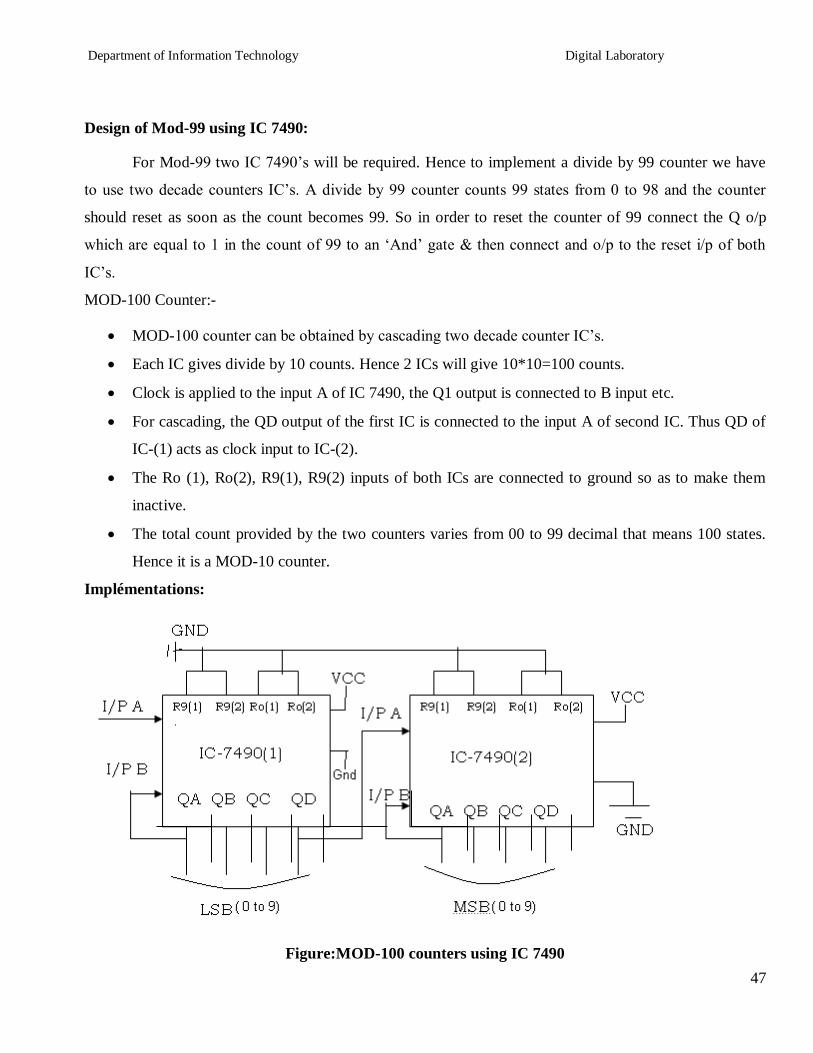
Department of Information Technology Digital Laboratory
47
Design of Mod-99 using IC 7490
For Mod-99 two IC 7490rsquos will be required Hence to implement a divide by 99 counter we have
to use two decade counters ICrsquos A divide by 99 counter counts 99 states from 0 to 98 and the counter
should reset as soon as the count becomes 99 So in order to reset the counter of 99 connect the Q op
which are equal to 1 in the count of 99 to an lsquoAndrsquo gate amp then connect and op to the reset ip of both
ICrsquos
MOD-100 Counter-
MOD-100 counter can be obtained by cascading two decade counter ICrsquos
Each IC gives divide by 10 counts Hence 2 ICs will give 1010=100 counts
Clock is applied to the input A of IC 7490 the Q1 output is connected to B input etc
For cascading the QD output of the first IC is connected to the input A of second IC Thus QD of
IC-(1) acts as clock input to IC-(2)
The Ro (1) Ro(2) R9(1) R9(2) inputs of both ICs are connected to ground so as to make them
inactive
The total count provided by the two counters varies from 00 to 99 decimal that means 100 states
Hence it is a MOD-10 counter
Impleacutementations
FigureMOD-100 counters using IC 7490
Department of Information Technology Digital Laboratory
48
B) IC 74191 ndash Theory
IC74191 is 4-bit binary synchronous reversible up down counter It contains 4 master slave flip flops
with internal gating and steering logic to provide asynchronous reset and synchronous count updown
operations its asynchronous parallel capability permits the counter to be preset to any desire number D0
to D3 are the parallel data inputs Information present on the parallel data inputs D0 to D3 is loaded into
the counter and appears on the output when the load PLinput is lowThisoperation overrides the counting
function Counting is inhabited by the high level on the enable G input when G input is low internal state
changes are initiated synchronously by the low to high transitions of the clock inputs the updown input
signal determines the direction of input
Function Table
Operating
mode
Inputs Outputs
PL UD G CLK Dn
Parallel
load L X X X L L
L X X X H H
Count up H L 0 uarr X Count up
Count
down H H 0 uarr X
Count
down
Hold(No
change) H X H X X No change
Pin details ndash
D0 to D3 input lines PL parallel load
G is Enable input ndash enabling the counting
Q0 to Q3 output lines
Downup determines the direction of counting
Clk clock input for counter
Terminal Count Max(1111) min(0000) For these states signal goes high for 1clock pulse
Ripple clock Clock input for next higher state
Department of Information Technology Digital Laboratory
49
Pin Diagram IC 74191
Up counter- Truth Table
Clk
Pulses QA QB QC QD
0 0 0 0 0
1 0 0 0 1
2 0 0 1 0
3 0 0 1 1
4 0 1 0 0
5 0 1 0 1
6 0 1 1 0
7 1 1 1 1
8 1 0 0 0
9 1 0 0 1
10 1 0 1 0
11 1 0 1 1
12 1 1 0 0
13 1 1 0 1
Department of Information Technology Digital Laboratory
50
14 1 1 1 0
15 1 1 1 1
Logic Diagram
Steps-
Connect the circuit as shown above
Apply clock ip to pin no14
Connect UD to GND
Verify the output according to truth table
Logic diagram of down counter
Steps-
Connect the circuit as shown above
Apply clock ip to pin no14
Connect UD to VCC
Verify the output according to truth table
UD D3 D2 D1 D0 PL
Clock IC 74191
G RC
MAX MIN
Q3 Q2 Q1 Q0 TC
vcc
NC
NC
Outputs
no connection
vcc
Department of Information Technology Digital Laboratory
51
With the help of IC74191 we can implement truncated updown counter by using following logic ndash
Connect data input line to particular count you want to load
According to requirement make Truth table
Draw the K-map
Find out Boolean expression
Draw the logic diagram and that is the combinational logic for your count and apply the output of
that circuit to PL
According to requirement we get the UP and down counting
5 Modulus n Counter
Presettable updown counter
Mod 11 counter
Implementation of presetttable mod updown counter using IC- 74LS191
1 Load Data on data lines D0 to D3 (0101)
2 Counter will go through the states from 0101 0110hellip1111 in up counter and 0101 to 0000 in
down counter
Combinational Circuit
CLOCK D3 D2 D1 D0
TC
U D 74191 RC
G PL
Updown Q3 Q2 Q1 Q0 PL
Q3 Q2 Q1 Q0
Preset Count
Department of Information Technology Digital Laboratory
52
3 The logic circuit should be designed in such a way that only when all the outputs are high output
of the reset circuit should be low and the counter should jump to state 5 It should again start
counting from 0101 to 0000
State Table
Down Counter UP Counter
IC 74191 is 4 bit counter Thus it counts 0000 to 1111 different 16 states For MOD11 counter we require
different 11 states so 5 steps must be skipped from 16 states We get MOD11 by presetting counter to
value 5
Assignment Question
Design and Implement MOD 7 MOD 10 and MOD 12 using IC 74191
FAQs
1 What do you mean modulus counter
Counter
state Clock
pulse
Q3 Q2 Q1 Q0
1 0 1 0 1
2 0 1 1 0
3 0 1 1 1
4 1 0 0 0
5 1 0 0 1
6 1 0 1 0
7 1 0 1 1
8 1 1 0 0
9 1 1 0 1
10 1 1 1 1
11 1 1 1 1
Counter state
Clock pulse
FF outputs
Q3 Q2 Q1 Q0
1 0 1 0 1
2 0 1 0 0
3 0 0 1 1
4 0 0 1 0
5 0 0 0 1
6 0 0 0 0
7 0 1 0 1
Department of Information Technology Digital Laboratory
53
It represents the number of possible states of counter
2 How will you use the 7490 IC to design symmetrical divide by 10 frequency counter
The divide by 5 circuit followed by divide by 2 circuit will give symmetrical output
3Where counters are used Give real life example of counter
Modulus n Counter
Binary counter ndash An N stage counter that recycles after 2 Ncount The count proceds in specified binary
sequence Counter Presetable- A counter which can be set to a desired value before the start of the
counting UPDown counter ndash A counter that can count in both up and down direction depending upon a
control input
Department of Information Technology Digital Laboratory
54
Regularity Content Viva-voce Timely
Submission Total
Dated Sign of
Subject
Teacher
2 4 2 2 10
Date of Performance Date of Completion
-------------------------------------------------------------------------------------------------------------------
Assignment No6
------------------------------------------------------------------------------------------------------------------
Title Sequence Generator
------------------------------------------------------------------------------------------------------------------
Objective To understand sequence generator one of the sequential circuit
-------------------------------------------------------------------------------------------------------------------
Problem Statement Design (State Diagram State Table K Map) and implementation of Sequence
Generator using Shift Register IC 74194
-----------------------------------------------------------------------------------------------------------------
Hardware Requirement
i) IC 741947408 (AND-gate) 7432 (OR-gate)
ii) Digital Trainer Kit -1
iii) Patch cords
----------------------------------------------------------------------------------------------------------------
Software Requirement Digital Work 30
------------------------------------------------------------------------------------------------------------------
Theory
Part A Sequence Generator with Flip flop
A sequential circuit which generates a prescribed sequence of bits in synchronism with a clock is referred
to as a sequence generator These pulse trains or sequence of bits can be used to open valves close gates
turn on lights and turn off machines and other variety of jobs
Department of Information Technology Digital Laboratory
55
For the design of sequence generator we first determine the required no of flip flops and the logic circuit
for the next state decoder
No of flip flops required to generate particular sequence can be determined as follows
1) Find the no of 1rsquos in the sequence
2) Find the no of 0rsquos in the sequence
3) Take the maximum out of two
4) If N is the required no of flip flops choose minimum value of lsquonrsquo to satisfy equation given below
Max (0rsquos 1rsquos) le 2n-1
The sequence generator can be classified as
1) sequence generator without bushing
2) sequence generator with bushing
The aim in this experiment is to design a sequence generator to generate a sequence of bit ie 10101
Part B Sequence Generator using Shift Register IC 74194
IC 74194 4 bit bidirectional Shift Register
This bidirectional shift register is designed to incorporate virtually all the features a system designer may
want in a shift register they feature Parallel inputs parallel outputs right shift left shift serialinputs
operating mode control inputsand a direct overriding clear line The register has four distinct modes of
operationsnamely
1 Parallel load
2 Shift right (in the direction QA towards QD)
3 Shift left (in the direction QD towards QA)
4 Inhibit clock (do nothing)
Synchronous parallel loading is accomplished by applying the four bits of data and taking both
mode control inputs S0 and S1High The data is loaded in to the associated flip-flops and appear
at the outputs after positive transition of the clock input During loading serial data flow is
inhibited
Shift right is accomplished synchronously with the rising edge of the clock pulse when S0 is High
and S1 is Low Serial data for this mode is entered at the shift right data input When S0 is Low
and S1 is High data shifts left synchronously and new data is entered at the shift left serial input
Clocking of the flip flop is inhibited when both mode control inputs are LOW
Department of Information Technology Digital Laboratory
56
Mode Control Input Operation
S1 S0
0 0 Clock Inhibit
0 1 Shift right
1 0 Shift Left
1 1 Parallel loading
Function Table of IC 74194
Design
The minimum number of flip-flops N required to generate a sequence of length S is given by S
le 2N ndash 1
In this case S=7 therefore the minimum value of N which may generate in this sequence is 3
However it is not guaranteed to lead to a solution If the given sequence leads to seven distinct
states then only three flip flops are sufficient otherwise we have to increase the number of flip
flops We write the states of circuit as given in table 1 The prescribed sequence is listed under QA
and the sequence listed under QB and QC are the same sequence delayed by one and two clock
pulses respectively From the table we observe that all the states are not distinct which means N=3
is not sufficient Next we assume that N=4 and prepare table 2 The last column gives the required
serial input for getting the desired change of state when a clock pulse is applied This is obtained
by assuming D type flip flop and looking at the QA output For example at the falling edge of first
clock pulse QA=1 The second clock pulse must result in QA=1 which requires its D input to be 1
In the same manner all the entries in column Y are determined
Table 1 State Assignment Table of Sequence Generator (N=3)
Number of Clock
Pulses
Flip Flop Inputs States
QA QB QC
1 1 1 1 7
2 1 1 1 7
3 0 1 1 3
4 1 0 1 5
Department of Information Technology Digital Laboratory
57
5 0 1 0 2
6 1 0 1 5
7 1 1 0 6
Excitation table of D Flip-Flop
Present State Qn Next State Qn+1 Flip-Flop Input D
0 0 0
0 1 1
1 0 0
1 1 1
Table 2State Assignment Table of Sequence Generator (N=4)
Number of Clock
Pulses
Flip Flop Inputs States
Y
Serial ip QA QB QC QD
1 1 1 1 0 14 1
2 1 1 1 1 15 0
3 0 1 1 1 7 1
4 1 0 1 1 11 0
5 0 1 0 1 5 1
6 1 0 1 0 10 1
7 1 1 0 1 13 1
K-Map Simplification
Department of Information Technology Digital Laboratory
58
00 01 11 10
00 X X X X
01 X 1 1 X
11 X 1 0 1
10 X X 0 1
Y= QArsquo + QBrsquo + QCrsquo = QAQBQC
LOGIC DIAGRAM
HARDWARE REQUIREMENTS
Sr no ICs Description Quantity
11 74194 4 bit bidirectional universal shift register 16ktr`
2 7410 3 input NAND Gate 1
Department of Information Technology Digital Laboratory
59
Conclusion In this way sequence generator using JK flip flips amp shift register is designed and
implemented
Enhancements Modifications ndash Sequence generator can also be implemented with shift register instead
of flip flops Use IC 7495 universal shift register IC and try to implement sequence generator
FAQs
1 What is sequential logic circuit
A sequential logic circuit consists of a memory elements in addition to
combinational circuit Its output at any instant of time depends upon
the present input as well as present state of memory element
2 What is meant by delay line
It is used to introduce time delays in digital signals
3 What is meant by following terms
a) Synchronous preset b) Asynchronous preset
c) Synchronous clear d) Asynchronous clear
a)Preset operation is synchronised with the clock
b)Preset operation is independent of the clock
c) clear is performed in synchronous with clock
d) clear is performed independent with clock
4 Is asynchronous counter faster than synchronous counter
In a synchronous counter the time required for change of any state is same and is equal to delay
time of one flip flop where as in asynchronous counter all flip flops are not clocked
simultaneously hence time required is not same
5 What is mean by lockout in counter
In a counter design for a fewer state than the maximum possible state some time it may so happen
that counter enters in unused state and goes from one unused state to another unused state and
never comes to used state
6 What is mean by state table
Department of Information Technology Digital Laboratory
60
It consists of complete information about present state and next state and outputs of a sequential
system
7 What is mean by state diagram
The information available in a state table can be represented as graphically the graphical
representation is known as state diagram
8 What is the advantage of state reduction in the design of sequential circuit
It reduces the number of flip flops
9 What is meant by excitation table
This gives information about what should be the flip flop inputs if outputs are specified before and
after the clock pulse
10 How many flip flops are required to design sequence generator using Counters
max (0rsquoS1rsquoS) in a given sequence lt= 2(N - 1)
Where N = Number of flip flops
11 How many flip flops are required to design sequence generator using shift registers
Slt= 2N - 1
Where N=Number of flip flops
S= Length of sequence
12 What is Lock out condition How it is avoided
When counter enters into one of the invalid state and after application of pulses remains in invalid
states only i e counter gets locked into invalid state amp this is called as lock out Lock out can be
avoided by providing bushing to all the invalid states in such a way that after application of one or
more clock pulses counter will fall into one of the valid state
Department of Information Technology Digital Laboratory
61
Regularity Content Viva-voce Timely
Submission Total
Dated Sign of
Subject
Teacher
2 4 2 2 10
Date of Performance Date of Completion
-------------------------------------------------------------------------------------------------------------------
Assignment No7
------------------------------------------------------------------------------------------------------------------
Title Multiplexer using Data flow modeling and structural modeling
------------------------------------------------------------------------------------------------------------------
Objective To learn data flow modeling style Its uses and different types of declarations with some
different types of circuits Structure of VHDL program is well discussed with this modeling style
-------------------------------------------------------------------------------------------------------------------
Problem Statement 41 multiplexer using data flow amp structural modeling -
----------------------------------------------------------------------------------------------------------------
Hardware Requirement - NA
----------------------------------------------------------------------------------------------------------------
Software Requirement Xilinx
------------------------------------------------------------------------------------------------------------------
Theory
Data flow style-
In this type of design the view of data as flowing from input to output through a design
An operation is defined in terms of a collection of data transformation expressed as concurrent
statement Each of the statement can be activated when any of its input signal changes its value While
these statements describe the behavior of the circuit a lot of information about its structure can be
extracted from the description as well
Data flow modeling has a set of concurrent assignment statements In the data flow level of abstraction we
describe how information is passed in the circuit The built in operators in VHDL are used in expression
such as AND OR XOR NOT etc
Department of Information Technology Digital Laboratory
62
INPUT
Two select lines S1S0
Four data lines D0 D1 D2 D3
OUTPUT
One output line Y
Functional block diagram of 41 Mux
Fig 41 Multiplexer using Data flow modeling
Function table of 41 Mux
Enable S1 S0 A B C D Y
1 X X X X X X 0
0 0 0 A X X X A
0 0 1 X B X X B
0 1 0 X X C X C
0 1 1 X X X D D
Design steps
Click on Xilinx ISE 92i
Create New project from file menu Ensure top level source is HDL
Select family of devices (usually spartan2E or 3)
Department of Information Technology Digital Laboratory
63
Ensure preferred language is VHDL
Click new source which shows you project details device details
and Synthesis and simulator tools
After finishing project create new source by right clicking in project name with VHDL
module
Complete ports name directions and bus Ensure architecture name is behavioral
After that we will get design summary and detailed reports
Close design summary
Create your code with given modeling style
Go to process window and synthesis to check if any error is there in code Check syntax and
view RTL schematic
Create new source to simulate the code
Right click on source name and create test bench waveform with proper name Ensure the
project is same
Click on combinational circuit in initial timing wizard
Select test bench wave in source window Apply inputs to wave diagram Ensure you are in
behavioral simulation
Go to process box Click on Xilinx ISE simulator and simulate the model See results
RTL Schematic
Department of Information Technology Digital Laboratory
64
Timing Diagram
FAQrsquos
1 What are the different kinds of data objects in VHDL code
Ans data object may be any value or number still some signal data objects and bit and bit_vector
types of these are available in VHDL STD_LOGIC and STD_LOGIC_VECTOR types are used
widely in programming
2 What do you mean by signal
Ans signal is a data object represents logic signals or wires in a circuit There are three places in
which signals can be declared in VHDL code in an entity declaration in the declarative section of
architecture and in declarative section of package
3 What are different signal types
Ans BIT BIT_VECTOR STD_LOGIC STD_LOGIC_VECTOR STD_ULOGIC SIGNED
UNSIGNED INTEGER ENUMERATION and BOOLEAN
4 What is an entity
Ans a circuit or sub circuit described with VHDL code is called a design entity
5 Explain structure of an entity
Ans it has two main parts the entity declaration which specifies the input and output signals for
entity and the architecture which gives circuit details
Department of Information Technology Digital Laboratory
65
6 How will you declare a package with component Explain structure
The general form of package declaration is as shown in diagram
PACKAGE package_name IS
[TYPE declarations]
[SIGNAL declarations]
[COMPONENT declarations]
END package_name
Entity
Declaration Architecture
Department of Information Technology Digital Laboratory
66
Regularity Content Viva-voce Timely
Submission Total
Dated Sign of
Subject
Teacher
2 4 2 2 10
Date of Performance Date of Completion
-------------------------------------------------------------------------------------------------------------------
Assignment No8
------------------------------------------------------------------------------------------------------------------
Title Full Adder using Behavioral and Structural modeling
------------------------------------------------------------------------------------------------------------------
Objective To learn structural modeling style Its uses and different types of declarations with some
different types of circuits Structure of VHDL program is well discussed with this modeling style
-------------------------------------------------------------------------------------------------------------------
Problem Statement Full adder using behavioral amp structural modeling
-----------------------------------------------------------------------------------------------------------------
Hardware Requirement - NA
----------------------------------------------------------------------------------------------------------------
Software Requirement Xilinx
------------------------------------------------------------------------------------------------------------------
Theory
Structural style-
A digital electronic system can be described as a module with inputs andor outputs The electrical values
on the outputs are same functions of the values of inputs The example of it is as shown The NAND gate
has 2ips AampB amp an output y Using VHDL terminology we call the NAND2 design entity amp the inputs
amp outputs are called ports 1 way of describing the function of NAND2 is to describe how it is composed
of sub modules AND amp INVERTER Each of the Sub modules is an instance of some entity amp ports of the
instances are connected using signals Structural modeling has a set of interconnected component
Structure can be used to create a very low level description of a circuit or a very high level description
Department of Information Technology Digital Laboratory
67
In a gate level description of a circuit for example components such as basic logic gates amp FFs might be
connected in some logical stricture to create the circuit This is what is often called a net list
Structure of structural modeling
Functional block diagram of Full Adder
architectureNetlistofHalf_Adderis
-- component with locals
componentMyXorport (A_XorB_Xor in BIT
Z_Xor out BIT)
end component
-- component with locals
componentMyAndport (A_AndB_And in BIT
Z_And out BIT)
end component
begin
Xor1 MyXorport map (X Y Sum)
-- instance with actuals
And1 MyAndport map (X Y Cout)
-- instance with actuals
end
Department of Information Technology Digital Laboratory
68
Function table of Full Adder
A B Cin SUM CARRY
0 0 0 0 0
0 0 1 1 0
0 1 0 1 0
0 1 1 0 1
1 0 0 1 0
1 0 1 0 1
1 1 0 0 1
1 1 1 1 1
Sum = Σm(1 2 4 7)
Carry= Σm(3 5 6 7)
Design steps
Click on Xilinx ISE 92i
Create New project from file menu Ensure top level source is HDL
Select family of devices (usually spartan2E or 3)
Ensure preferred language is VHDL
Click new source which shows you project details device details
and Synthesis and simulator tools
After finishing project create new source(full adder) by right clicking in project name with
VHDL module
Complete ports name directions and bus Ensure architecture name is behavioral
After that we will get design summary and detailed reports
Close design summary
Click new source which shows you project details device details
and Synthesis and simulator tools
After finishing project create new source(half adder) by right clicking in project name with
VHDL module
Complete ports name directions and bus Ensure architecture name is behavioral Names
should be same as previous inputs
Department of Information Technology Digital Laboratory
69
After that we will get design summary and detailed reports
Close design summary
Create your code for half adder with given modeling style
After that go to process window Click on design utilities
View HDL instantiation code of half adder
Copy component part of half adder in architecture block of full adder Copy instantiation
template twice after begin as we require two half adders to construct full adder (structural
modeling) Name them differently (eg ha1 or ha2)
Create signals as per the logic Complete code of full adder
Go to process window and synthesis to check if any error is there in code Check syntax and
view RTL schematic
Create new source to simulate the code
Right click on source name and create test bench waveform with proper name Ensure the
project is same
Click on combinational circuit in initial timing wizard
Select test bench wave in source window Apply inputs to wave diagram Ensure you are in
behavioral simulation
Go to process box Click on Xilinx ISE simulator and simulate the model See results
RTL Schematic
Timing Diagram
Department of Information Technology Digital Laboratory
70
INPUT
Three inputs A B Carry (previous)
OUTPUT
Two outputs Sum Carry
FAQrsquos
1 What do you mean by structural style
Ans in this type of code a circuit is described in hierarchical fashion by connecting together sub
circuits
2 Explain IF statement with example
Ans The general form of an IF statement is as follws
IF Sel=rsquo0rsquo THEN
Flt=x1
ELSE
Flt=x2
END IF
Department of Information Technology Digital Laboratory
71
3 Explain declaration and instantiation process in VHDL
Ans first declare a small vhdl code in formal way Eg half adder Define project name is full adder
And simply copy instantiation template in main source code Define how many times you want to
declare this template Give separate names for those
4 What is STD_LOGIC_VECTOR
Ans It is standard data object added to VHDL standard in IEEE 1164 It provides more flexibility
than the Bit type
5 Explain difference between concurrent and sequential statements
Ans Concurrent statements define interconnected processes and blocks that together describe a designrsquos
overall behavior or structure They can be grouped using block sstatement Groups of blocks can also be
partitioned into other blocks At this same level a VHDL component can be connected to define signals
within the blocks
It is a reference to an entity A process can be a single signal assignment statement or a series of
sequential statements (SS) Within a process procedures and functions can partition the sequential
statements
PRACTICE ASSIGNMENTS
1 Implement half adder using data flow modeling
2 Implement Full Adder using behavioral modeling
3 Implement 3 bit magnitude comparator using a 3 bit adder
4 Implement half sub tractor using data flow modeling
5 Write VHDL code for Full Subtractor
Department of Information Technology Digital Laboratory
72
Regularity Content Viva-voce Timely
Submission Total
Dated Sign of
Subject
Teacher
2 4 2 2 10
rsquozaDate of Performance Date of Completion
-------------------------------------------------------------------------------------------------------------------
Assignment No9
------------------------------------------------------------------------------------------------------------------
Title Simulation of 3 bit Connter using Behavioral modeling
------------------------------------------------------------------------------------------------------------------
Objective To learn behavioral modeling style Its uses and different types of declarations with some
different types of circuits Structure of VHDL program is well discussed with this modeling style
-------------------------------------------------------------------------------------------------------------------
Problem Statement 3 bit controlled up down synchronous counter with preset amp clear
-----------------------------------------------------------------------------------------------------------------
Hardware Requirement -NA
----------------------------------------------------------------------------------------------------------------
Software Requirement Xilinx
------------------------------------------------------------------------------------------------------------------
Theory
Behavioral style-
Highest level of abstraction supported in VHDL is called the behavior level of abstraction In it we have
for loop while loop If then else case ampvariable assignment The statements are enclosed in a PROCESS
block amp are executed sequentially
In it circuit is described in terms of its operation overtime
In behavioral description the concept of time may be expressed precisely with actual delays between
related events (such as the propagation delays within gates amp on wires) or it may be simply an ordering of
operation that are expressed sequentially (such as in a functional description of a FF)
Department of Information Technology Digital Laboratory
73
A behavioral design method defines a circuit in terms of text language rather than a schematic of
interconnected symbols
Behavioral design is a technology independent text based design that incorporates high level
functionality amp high level information flow
Structure of Behavioral modeling
Functional block diagram of 3 bit controlled up down synchronous counter with preset amp clear
Function table of 3 bit controlled up down synchronous counter with preset amp clear
Design steps
Click on Xilinx ISE 92i
Create New project from file menu Ensure top level source is HDL
Select family of devices (usually spartan2E or 3)
Ensure preferred language is VHDL
Click new source which shows you project details device details
and Synthesis and simulator tools
After finishing project create new source by right clicking in project name with VHDL
module
Complete ports name directions and bus Ensure architecture name is behavioral
After that we will get design summary and detailed reports
Close design summary
Create your code with given modeling style
Go to process window and synthesis to check if any error is there in code Check syntax
and view RTL schematic Create new source to simulate the code
Department of Information Technology Digital Laboratory
74
Right click on source name and create test bench waveform with proper name Ensure the
project is same
Click on combinational circuit in initial timing wizard
Select test bench wave in source window Apply inputs to wave diagram Ensure you are in
behavioral simulation
Go to process box Click on Xilinx ISE simulator and simulate the model
RTL Schematic
Timing Diagram
INPUT
Clock Preset Clear
OUTPUT
Three output lines
FAQrsquos
1 Explain the structure of behavioral modeling
2 What are the differences between behavioral and structural modeling
Ans Behavioral descriptionof a circuit is the highest level of abstraction in VHDL Here the
circuit is described in terms of it operation with respect to time All operations are in one level of
code The operations are described in a way that the designer of a sequential circuit infers a
register
Structural description on the other hand is a circuit description in terms of its components
it can either create a low level description much like a hierarchy in a block diagram Whenever
you see a component instantiated in a code that code employs structural description of the circuit
The components are connected in the form of a netlist This is for better manageability and
reusability
3 What are the differences between behavioral and data flow modeling
Department of Information Technology Digital Laboratory
75
Ans Behavioral ndash describes how the output is derived from the inputs using structured
statements
Dataflow ndash describes how the data flows from the inputs to the output most often
using NOT AND and OR operations
4 What do you mean by process statement
Ans The process statement begins with the PROCESS keyword followed by a parenthesized list
of signals called the sensitivity list It operates on selected and conditional statements
5 Explain syntax of process statement
Ans BEGIN
Process( sensitivity list)
END process
PRACTICE ASSIGNMENTS
1 Implement 3 bit asynchronous up counter using behavioral modeling
2 Implement 3 bit asynchronous down counter using behavioral modeling
3 Implement 3 bit synchronous down counter using behavioral modeling
End
Department of Information Technology Digital Laboratory
76
Pin Diagrams
7400 Quad 2-Input NAND Gate
7402 Quad 2-Input NOR Gate
7404 Not Gates
7408 Quad 2-Input AND Gates
7432 Quad 2-Input OR Gate
7486 Quad 2-Input Exclusive-OR Gate
Department of Information Technology Digital Laboratory
77
7483 4 bit Binary Adder
7490 Decade and Binary Counters
74138 38 Decoder
Department of Information Technology Digital Laboratory
78
74153 Dual 41 Multiplexer
74191 Synchronous UpDown 4 bit Binary counter with Mode Control
Department of Information Technology Digital Laboratory
79
74194 Universal Shift Register
7476 Dual Master-Slave J-K Flip-Flops
- Part B Sequence Generator using Shift Register IC 74194
-
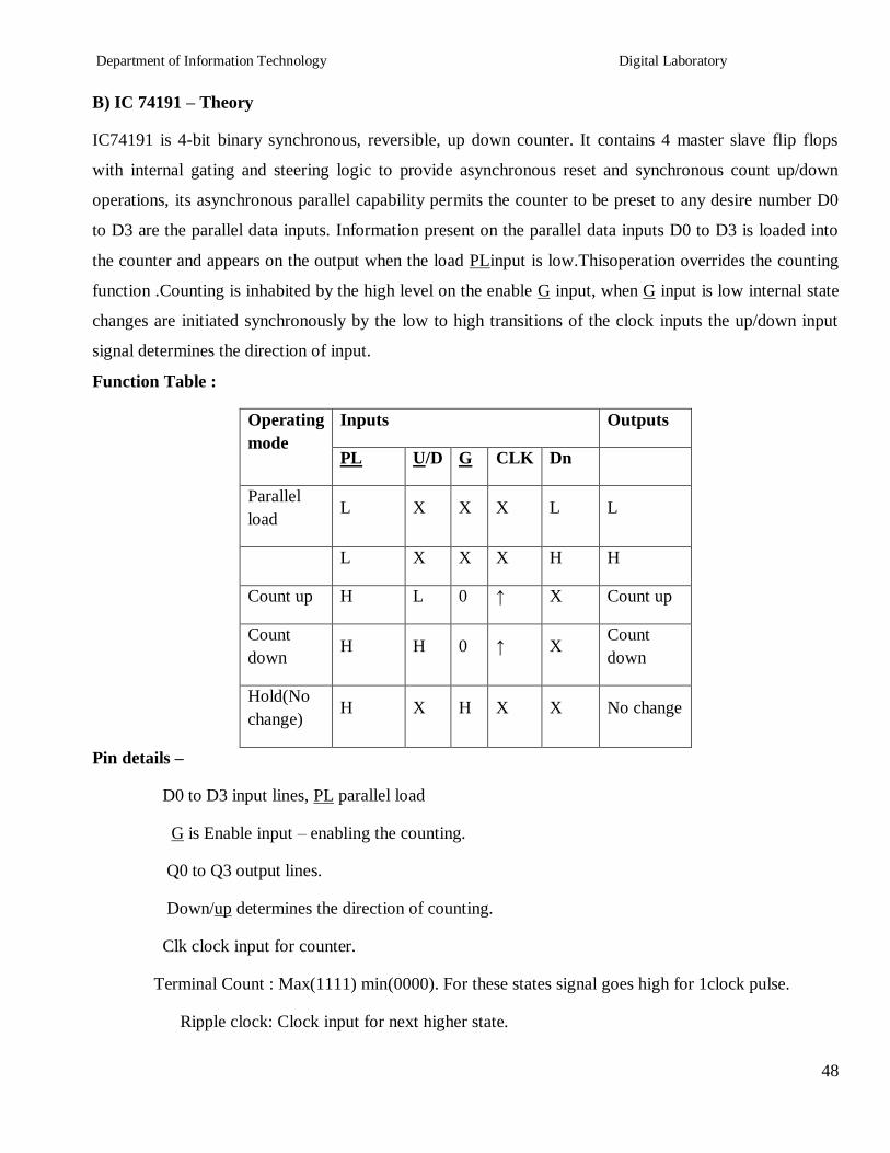
Department of Information Technology Digital Laboratory
49
Pin Diagram IC 74191
Up counter- Truth Table
Clk
Pulses QA QB QC QD
0 0 0 0 0
1 0 0 0 1
2 0 0 1 0
3 0 0 1 1
4 0 1 0 0
5 0 1 0 1
6 0 1 1 0
7 1 1 1 1
8 1 0 0 0
9 1 0 0 1
10 1 0 1 0
11 1 0 1 1
12 1 1 0 0
13 1 1 0 1
Department of Information Technology Digital Laboratory
50
14 1 1 1 0
15 1 1 1 1
Logic Diagram
Steps-
Connect the circuit as shown above
Apply clock ip to pin no14
Connect UD to GND
Verify the output according to truth table
Logic diagram of down counter
Steps-
Connect the circuit as shown above
Apply clock ip to pin no14
Connect UD to VCC
Verify the output according to truth table
UD D3 D2 D1 D0 PL
Clock IC 74191
G RC
MAX MIN
Q3 Q2 Q1 Q0 TC
vcc
NC
NC
Outputs
no connection
vcc
Department of Information Technology Digital Laboratory
51
With the help of IC74191 we can implement truncated updown counter by using following logic ndash
Connect data input line to particular count you want to load
According to requirement make Truth table
Draw the K-map
Find out Boolean expression
Draw the logic diagram and that is the combinational logic for your count and apply the output of
that circuit to PL
According to requirement we get the UP and down counting
5 Modulus n Counter
Presettable updown counter
Mod 11 counter
Implementation of presetttable mod updown counter using IC- 74LS191
1 Load Data on data lines D0 to D3 (0101)
2 Counter will go through the states from 0101 0110hellip1111 in up counter and 0101 to 0000 in
down counter
Combinational Circuit
CLOCK D3 D2 D1 D0
TC
U D 74191 RC
G PL
Updown Q3 Q2 Q1 Q0 PL
Q3 Q2 Q1 Q0
Preset Count
Department of Information Technology Digital Laboratory
52
3 The logic circuit should be designed in such a way that only when all the outputs are high output
of the reset circuit should be low and the counter should jump to state 5 It should again start
counting from 0101 to 0000
State Table
Down Counter UP Counter
IC 74191 is 4 bit counter Thus it counts 0000 to 1111 different 16 states For MOD11 counter we require
different 11 states so 5 steps must be skipped from 16 states We get MOD11 by presetting counter to
value 5
Assignment Question
Design and Implement MOD 7 MOD 10 and MOD 12 using IC 74191
FAQs
1 What do you mean modulus counter
Counter
state Clock
pulse
Q3 Q2 Q1 Q0
1 0 1 0 1
2 0 1 1 0
3 0 1 1 1
4 1 0 0 0
5 1 0 0 1
6 1 0 1 0
7 1 0 1 1
8 1 1 0 0
9 1 1 0 1
10 1 1 1 1
11 1 1 1 1
Counter state
Clock pulse
FF outputs
Q3 Q2 Q1 Q0
1 0 1 0 1
2 0 1 0 0
3 0 0 1 1
4 0 0 1 0
5 0 0 0 1
6 0 0 0 0
7 0 1 0 1
Department of Information Technology Digital Laboratory
53
It represents the number of possible states of counter
2 How will you use the 7490 IC to design symmetrical divide by 10 frequency counter
The divide by 5 circuit followed by divide by 2 circuit will give symmetrical output
3Where counters are used Give real life example of counter
Modulus n Counter
Binary counter ndash An N stage counter that recycles after 2 Ncount The count proceds in specified binary
sequence Counter Presetable- A counter which can be set to a desired value before the start of the
counting UPDown counter ndash A counter that can count in both up and down direction depending upon a
control input
Department of Information Technology Digital Laboratory
54
Regularity Content Viva-voce Timely
Submission Total
Dated Sign of
Subject
Teacher
2 4 2 2 10
Date of Performance Date of Completion
-------------------------------------------------------------------------------------------------------------------
Assignment No6
------------------------------------------------------------------------------------------------------------------
Title Sequence Generator
------------------------------------------------------------------------------------------------------------------
Objective To understand sequence generator one of the sequential circuit
-------------------------------------------------------------------------------------------------------------------
Problem Statement Design (State Diagram State Table K Map) and implementation of Sequence
Generator using Shift Register IC 74194
-----------------------------------------------------------------------------------------------------------------
Hardware Requirement
i) IC 741947408 (AND-gate) 7432 (OR-gate)
ii) Digital Trainer Kit -1
iii) Patch cords
----------------------------------------------------------------------------------------------------------------
Software Requirement Digital Work 30
------------------------------------------------------------------------------------------------------------------
Theory
Part A Sequence Generator with Flip flop
A sequential circuit which generates a prescribed sequence of bits in synchronism with a clock is referred
to as a sequence generator These pulse trains or sequence of bits can be used to open valves close gates
turn on lights and turn off machines and other variety of jobs
Department of Information Technology Digital Laboratory
55
For the design of sequence generator we first determine the required no of flip flops and the logic circuit
for the next state decoder
No of flip flops required to generate particular sequence can be determined as follows
1) Find the no of 1rsquos in the sequence
2) Find the no of 0rsquos in the sequence
3) Take the maximum out of two
4) If N is the required no of flip flops choose minimum value of lsquonrsquo to satisfy equation given below
Max (0rsquos 1rsquos) le 2n-1
The sequence generator can be classified as
1) sequence generator without bushing
2) sequence generator with bushing
The aim in this experiment is to design a sequence generator to generate a sequence of bit ie 10101
Part B Sequence Generator using Shift Register IC 74194
IC 74194 4 bit bidirectional Shift Register
This bidirectional shift register is designed to incorporate virtually all the features a system designer may
want in a shift register they feature Parallel inputs parallel outputs right shift left shift serialinputs
operating mode control inputsand a direct overriding clear line The register has four distinct modes of
operationsnamely
1 Parallel load
2 Shift right (in the direction QA towards QD)
3 Shift left (in the direction QD towards QA)
4 Inhibit clock (do nothing)
Synchronous parallel loading is accomplished by applying the four bits of data and taking both
mode control inputs S0 and S1High The data is loaded in to the associated flip-flops and appear
at the outputs after positive transition of the clock input During loading serial data flow is
inhibited
Shift right is accomplished synchronously with the rising edge of the clock pulse when S0 is High
and S1 is Low Serial data for this mode is entered at the shift right data input When S0 is Low
and S1 is High data shifts left synchronously and new data is entered at the shift left serial input
Clocking of the flip flop is inhibited when both mode control inputs are LOW
Department of Information Technology Digital Laboratory
56
Mode Control Input Operation
S1 S0
0 0 Clock Inhibit
0 1 Shift right
1 0 Shift Left
1 1 Parallel loading
Function Table of IC 74194
Design
The minimum number of flip-flops N required to generate a sequence of length S is given by S
le 2N ndash 1
In this case S=7 therefore the minimum value of N which may generate in this sequence is 3
However it is not guaranteed to lead to a solution If the given sequence leads to seven distinct
states then only three flip flops are sufficient otherwise we have to increase the number of flip
flops We write the states of circuit as given in table 1 The prescribed sequence is listed under QA
and the sequence listed under QB and QC are the same sequence delayed by one and two clock
pulses respectively From the table we observe that all the states are not distinct which means N=3
is not sufficient Next we assume that N=4 and prepare table 2 The last column gives the required
serial input for getting the desired change of state when a clock pulse is applied This is obtained
by assuming D type flip flop and looking at the QA output For example at the falling edge of first
clock pulse QA=1 The second clock pulse must result in QA=1 which requires its D input to be 1
In the same manner all the entries in column Y are determined
Table 1 State Assignment Table of Sequence Generator (N=3)
Number of Clock
Pulses
Flip Flop Inputs States
QA QB QC
1 1 1 1 7
2 1 1 1 7
3 0 1 1 3
4 1 0 1 5
Department of Information Technology Digital Laboratory
57
5 0 1 0 2
6 1 0 1 5
7 1 1 0 6
Excitation table of D Flip-Flop
Present State Qn Next State Qn+1 Flip-Flop Input D
0 0 0
0 1 1
1 0 0
1 1 1
Table 2State Assignment Table of Sequence Generator (N=4)
Number of Clock
Pulses
Flip Flop Inputs States
Y
Serial ip QA QB QC QD
1 1 1 1 0 14 1
2 1 1 1 1 15 0
3 0 1 1 1 7 1
4 1 0 1 1 11 0
5 0 1 0 1 5 1
6 1 0 1 0 10 1
7 1 1 0 1 13 1
K-Map Simplification
Department of Information Technology Digital Laboratory
58
00 01 11 10
00 X X X X
01 X 1 1 X
11 X 1 0 1
10 X X 0 1
Y= QArsquo + QBrsquo + QCrsquo = QAQBQC
LOGIC DIAGRAM
HARDWARE REQUIREMENTS
Sr no ICs Description Quantity
11 74194 4 bit bidirectional universal shift register 16ktr`
2 7410 3 input NAND Gate 1
Department of Information Technology Digital Laboratory
59
Conclusion In this way sequence generator using JK flip flips amp shift register is designed and
implemented
Enhancements Modifications ndash Sequence generator can also be implemented with shift register instead
of flip flops Use IC 7495 universal shift register IC and try to implement sequence generator
FAQs
1 What is sequential logic circuit
A sequential logic circuit consists of a memory elements in addition to
combinational circuit Its output at any instant of time depends upon
the present input as well as present state of memory element
2 What is meant by delay line
It is used to introduce time delays in digital signals
3 What is meant by following terms
a) Synchronous preset b) Asynchronous preset
c) Synchronous clear d) Asynchronous clear
a)Preset operation is synchronised with the clock
b)Preset operation is independent of the clock
c) clear is performed in synchronous with clock
d) clear is performed independent with clock
4 Is asynchronous counter faster than synchronous counter
In a synchronous counter the time required for change of any state is same and is equal to delay
time of one flip flop where as in asynchronous counter all flip flops are not clocked
simultaneously hence time required is not same
5 What is mean by lockout in counter
In a counter design for a fewer state than the maximum possible state some time it may so happen
that counter enters in unused state and goes from one unused state to another unused state and
never comes to used state
6 What is mean by state table
Department of Information Technology Digital Laboratory
60
It consists of complete information about present state and next state and outputs of a sequential
system
7 What is mean by state diagram
The information available in a state table can be represented as graphically the graphical
representation is known as state diagram
8 What is the advantage of state reduction in the design of sequential circuit
It reduces the number of flip flops
9 What is meant by excitation table
This gives information about what should be the flip flop inputs if outputs are specified before and
after the clock pulse
10 How many flip flops are required to design sequence generator using Counters
max (0rsquoS1rsquoS) in a given sequence lt= 2(N - 1)
Where N = Number of flip flops
11 How many flip flops are required to design sequence generator using shift registers
Slt= 2N - 1
Where N=Number of flip flops
S= Length of sequence
12 What is Lock out condition How it is avoided
When counter enters into one of the invalid state and after application of pulses remains in invalid
states only i e counter gets locked into invalid state amp this is called as lock out Lock out can be
avoided by providing bushing to all the invalid states in such a way that after application of one or
more clock pulses counter will fall into one of the valid state
Department of Information Technology Digital Laboratory
61
Regularity Content Viva-voce Timely
Submission Total
Dated Sign of
Subject
Teacher
2 4 2 2 10
Date of Performance Date of Completion
-------------------------------------------------------------------------------------------------------------------
Assignment No7
------------------------------------------------------------------------------------------------------------------
Title Multiplexer using Data flow modeling and structural modeling
------------------------------------------------------------------------------------------------------------------
Objective To learn data flow modeling style Its uses and different types of declarations with some
different types of circuits Structure of VHDL program is well discussed with this modeling style
-------------------------------------------------------------------------------------------------------------------
Problem Statement 41 multiplexer using data flow amp structural modeling -
----------------------------------------------------------------------------------------------------------------
Hardware Requirement - NA
----------------------------------------------------------------------------------------------------------------
Software Requirement Xilinx
------------------------------------------------------------------------------------------------------------------
Theory
Data flow style-
In this type of design the view of data as flowing from input to output through a design
An operation is defined in terms of a collection of data transformation expressed as concurrent
statement Each of the statement can be activated when any of its input signal changes its value While
these statements describe the behavior of the circuit a lot of information about its structure can be
extracted from the description as well
Data flow modeling has a set of concurrent assignment statements In the data flow level of abstraction we
describe how information is passed in the circuit The built in operators in VHDL are used in expression
such as AND OR XOR NOT etc
Department of Information Technology Digital Laboratory
62
INPUT
Two select lines S1S0
Four data lines D0 D1 D2 D3
OUTPUT
One output line Y
Functional block diagram of 41 Mux
Fig 41 Multiplexer using Data flow modeling
Function table of 41 Mux
Enable S1 S0 A B C D Y
1 X X X X X X 0
0 0 0 A X X X A
0 0 1 X B X X B
0 1 0 X X C X C
0 1 1 X X X D D
Design steps
Click on Xilinx ISE 92i
Create New project from file menu Ensure top level source is HDL
Select family of devices (usually spartan2E or 3)
Department of Information Technology Digital Laboratory
63
Ensure preferred language is VHDL
Click new source which shows you project details device details
and Synthesis and simulator tools
After finishing project create new source by right clicking in project name with VHDL
module
Complete ports name directions and bus Ensure architecture name is behavioral
After that we will get design summary and detailed reports
Close design summary
Create your code with given modeling style
Go to process window and synthesis to check if any error is there in code Check syntax and
view RTL schematic
Create new source to simulate the code
Right click on source name and create test bench waveform with proper name Ensure the
project is same
Click on combinational circuit in initial timing wizard
Select test bench wave in source window Apply inputs to wave diagram Ensure you are in
behavioral simulation
Go to process box Click on Xilinx ISE simulator and simulate the model See results
RTL Schematic
Department of Information Technology Digital Laboratory
64
Timing Diagram
FAQrsquos
1 What are the different kinds of data objects in VHDL code
Ans data object may be any value or number still some signal data objects and bit and bit_vector
types of these are available in VHDL STD_LOGIC and STD_LOGIC_VECTOR types are used
widely in programming
2 What do you mean by signal
Ans signal is a data object represents logic signals or wires in a circuit There are three places in
which signals can be declared in VHDL code in an entity declaration in the declarative section of
architecture and in declarative section of package
3 What are different signal types
Ans BIT BIT_VECTOR STD_LOGIC STD_LOGIC_VECTOR STD_ULOGIC SIGNED
UNSIGNED INTEGER ENUMERATION and BOOLEAN
4 What is an entity
Ans a circuit or sub circuit described with VHDL code is called a design entity
5 Explain structure of an entity
Ans it has two main parts the entity declaration which specifies the input and output signals for
entity and the architecture which gives circuit details
Department of Information Technology Digital Laboratory
65
6 How will you declare a package with component Explain structure
The general form of package declaration is as shown in diagram
PACKAGE package_name IS
[TYPE declarations]
[SIGNAL declarations]
[COMPONENT declarations]
END package_name
Entity
Declaration Architecture
Department of Information Technology Digital Laboratory
66
Regularity Content Viva-voce Timely
Submission Total
Dated Sign of
Subject
Teacher
2 4 2 2 10
Date of Performance Date of Completion
-------------------------------------------------------------------------------------------------------------------
Assignment No8
------------------------------------------------------------------------------------------------------------------
Title Full Adder using Behavioral and Structural modeling
------------------------------------------------------------------------------------------------------------------
Objective To learn structural modeling style Its uses and different types of declarations with some
different types of circuits Structure of VHDL program is well discussed with this modeling style
-------------------------------------------------------------------------------------------------------------------
Problem Statement Full adder using behavioral amp structural modeling
-----------------------------------------------------------------------------------------------------------------
Hardware Requirement - NA
----------------------------------------------------------------------------------------------------------------
Software Requirement Xilinx
------------------------------------------------------------------------------------------------------------------
Theory
Structural style-
A digital electronic system can be described as a module with inputs andor outputs The electrical values
on the outputs are same functions of the values of inputs The example of it is as shown The NAND gate
has 2ips AampB amp an output y Using VHDL terminology we call the NAND2 design entity amp the inputs
amp outputs are called ports 1 way of describing the function of NAND2 is to describe how it is composed
of sub modules AND amp INVERTER Each of the Sub modules is an instance of some entity amp ports of the
instances are connected using signals Structural modeling has a set of interconnected component
Structure can be used to create a very low level description of a circuit or a very high level description
Department of Information Technology Digital Laboratory
67
In a gate level description of a circuit for example components such as basic logic gates amp FFs might be
connected in some logical stricture to create the circuit This is what is often called a net list
Structure of structural modeling
Functional block diagram of Full Adder
architectureNetlistofHalf_Adderis
-- component with locals
componentMyXorport (A_XorB_Xor in BIT
Z_Xor out BIT)
end component
-- component with locals
componentMyAndport (A_AndB_And in BIT
Z_And out BIT)
end component
begin
Xor1 MyXorport map (X Y Sum)
-- instance with actuals
And1 MyAndport map (X Y Cout)
-- instance with actuals
end
Department of Information Technology Digital Laboratory
68
Function table of Full Adder
A B Cin SUM CARRY
0 0 0 0 0
0 0 1 1 0
0 1 0 1 0
0 1 1 0 1
1 0 0 1 0
1 0 1 0 1
1 1 0 0 1
1 1 1 1 1
Sum = Σm(1 2 4 7)
Carry= Σm(3 5 6 7)
Design steps
Click on Xilinx ISE 92i
Create New project from file menu Ensure top level source is HDL
Select family of devices (usually spartan2E or 3)
Ensure preferred language is VHDL
Click new source which shows you project details device details
and Synthesis and simulator tools
After finishing project create new source(full adder) by right clicking in project name with
VHDL module
Complete ports name directions and bus Ensure architecture name is behavioral
After that we will get design summary and detailed reports
Close design summary
Click new source which shows you project details device details
and Synthesis and simulator tools
After finishing project create new source(half adder) by right clicking in project name with
VHDL module
Complete ports name directions and bus Ensure architecture name is behavioral Names
should be same as previous inputs
Department of Information Technology Digital Laboratory
69
After that we will get design summary and detailed reports
Close design summary
Create your code for half adder with given modeling style
After that go to process window Click on design utilities
View HDL instantiation code of half adder
Copy component part of half adder in architecture block of full adder Copy instantiation
template twice after begin as we require two half adders to construct full adder (structural
modeling) Name them differently (eg ha1 or ha2)
Create signals as per the logic Complete code of full adder
Go to process window and synthesis to check if any error is there in code Check syntax and
view RTL schematic
Create new source to simulate the code
Right click on source name and create test bench waveform with proper name Ensure the
project is same
Click on combinational circuit in initial timing wizard
Select test bench wave in source window Apply inputs to wave diagram Ensure you are in
behavioral simulation
Go to process box Click on Xilinx ISE simulator and simulate the model See results
RTL Schematic
Timing Diagram
Department of Information Technology Digital Laboratory
70
INPUT
Three inputs A B Carry (previous)
OUTPUT
Two outputs Sum Carry
FAQrsquos
1 What do you mean by structural style
Ans in this type of code a circuit is described in hierarchical fashion by connecting together sub
circuits
2 Explain IF statement with example
Ans The general form of an IF statement is as follws
IF Sel=rsquo0rsquo THEN
Flt=x1
ELSE
Flt=x2
END IF
Department of Information Technology Digital Laboratory
71
3 Explain declaration and instantiation process in VHDL
Ans first declare a small vhdl code in formal way Eg half adder Define project name is full adder
And simply copy instantiation template in main source code Define how many times you want to
declare this template Give separate names for those
4 What is STD_LOGIC_VECTOR
Ans It is standard data object added to VHDL standard in IEEE 1164 It provides more flexibility
than the Bit type
5 Explain difference between concurrent and sequential statements
Ans Concurrent statements define interconnected processes and blocks that together describe a designrsquos
overall behavior or structure They can be grouped using block sstatement Groups of blocks can also be
partitioned into other blocks At this same level a VHDL component can be connected to define signals
within the blocks
It is a reference to an entity A process can be a single signal assignment statement or a series of
sequential statements (SS) Within a process procedures and functions can partition the sequential
statements
PRACTICE ASSIGNMENTS
1 Implement half adder using data flow modeling
2 Implement Full Adder using behavioral modeling
3 Implement 3 bit magnitude comparator using a 3 bit adder
4 Implement half sub tractor using data flow modeling
5 Write VHDL code for Full Subtractor
Department of Information Technology Digital Laboratory
72
Regularity Content Viva-voce Timely
Submission Total
Dated Sign of
Subject
Teacher
2 4 2 2 10
rsquozaDate of Performance Date of Completion
-------------------------------------------------------------------------------------------------------------------
Assignment No9
------------------------------------------------------------------------------------------------------------------
Title Simulation of 3 bit Connter using Behavioral modeling
------------------------------------------------------------------------------------------------------------------
Objective To learn behavioral modeling style Its uses and different types of declarations with some
different types of circuits Structure of VHDL program is well discussed with this modeling style
-------------------------------------------------------------------------------------------------------------------
Problem Statement 3 bit controlled up down synchronous counter with preset amp clear
-----------------------------------------------------------------------------------------------------------------
Hardware Requirement -NA
----------------------------------------------------------------------------------------------------------------
Software Requirement Xilinx
------------------------------------------------------------------------------------------------------------------
Theory
Behavioral style-
Highest level of abstraction supported in VHDL is called the behavior level of abstraction In it we have
for loop while loop If then else case ampvariable assignment The statements are enclosed in a PROCESS
block amp are executed sequentially
In it circuit is described in terms of its operation overtime
In behavioral description the concept of time may be expressed precisely with actual delays between
related events (such as the propagation delays within gates amp on wires) or it may be simply an ordering of
operation that are expressed sequentially (such as in a functional description of a FF)
Department of Information Technology Digital Laboratory
73
A behavioral design method defines a circuit in terms of text language rather than a schematic of
interconnected symbols
Behavioral design is a technology independent text based design that incorporates high level
functionality amp high level information flow
Structure of Behavioral modeling
Functional block diagram of 3 bit controlled up down synchronous counter with preset amp clear
Function table of 3 bit controlled up down synchronous counter with preset amp clear
Design steps
Click on Xilinx ISE 92i
Create New project from file menu Ensure top level source is HDL
Select family of devices (usually spartan2E or 3)
Ensure preferred language is VHDL
Click new source which shows you project details device details
and Synthesis and simulator tools
After finishing project create new source by right clicking in project name with VHDL
module
Complete ports name directions and bus Ensure architecture name is behavioral
After that we will get design summary and detailed reports
Close design summary
Create your code with given modeling style
Go to process window and synthesis to check if any error is there in code Check syntax
and view RTL schematic Create new source to simulate the code
Department of Information Technology Digital Laboratory
74
Right click on source name and create test bench waveform with proper name Ensure the
project is same
Click on combinational circuit in initial timing wizard
Select test bench wave in source window Apply inputs to wave diagram Ensure you are in
behavioral simulation
Go to process box Click on Xilinx ISE simulator and simulate the model
RTL Schematic
Timing Diagram
INPUT
Clock Preset Clear
OUTPUT
Three output lines
FAQrsquos
1 Explain the structure of behavioral modeling
2 What are the differences between behavioral and structural modeling
Ans Behavioral descriptionof a circuit is the highest level of abstraction in VHDL Here the
circuit is described in terms of it operation with respect to time All operations are in one level of
code The operations are described in a way that the designer of a sequential circuit infers a
register
Structural description on the other hand is a circuit description in terms of its components
it can either create a low level description much like a hierarchy in a block diagram Whenever
you see a component instantiated in a code that code employs structural description of the circuit
The components are connected in the form of a netlist This is for better manageability and
reusability
3 What are the differences between behavioral and data flow modeling
Department of Information Technology Digital Laboratory
75
Ans Behavioral ndash describes how the output is derived from the inputs using structured
statements
Dataflow ndash describes how the data flows from the inputs to the output most often
using NOT AND and OR operations
4 What do you mean by process statement
Ans The process statement begins with the PROCESS keyword followed by a parenthesized list
of signals called the sensitivity list It operates on selected and conditional statements
5 Explain syntax of process statement
Ans BEGIN
Process( sensitivity list)
END process
PRACTICE ASSIGNMENTS
1 Implement 3 bit asynchronous up counter using behavioral modeling
2 Implement 3 bit asynchronous down counter using behavioral modeling
3 Implement 3 bit synchronous down counter using behavioral modeling
End
Department of Information Technology Digital Laboratory
76
Pin Diagrams
7400 Quad 2-Input NAND Gate
7402 Quad 2-Input NOR Gate
7404 Not Gates
7408 Quad 2-Input AND Gates
7432 Quad 2-Input OR Gate
7486 Quad 2-Input Exclusive-OR Gate
Department of Information Technology Digital Laboratory
77
7483 4 bit Binary Adder
7490 Decade and Binary Counters
74138 38 Decoder
Department of Information Technology Digital Laboratory
78
74153 Dual 41 Multiplexer
74191 Synchronous UpDown 4 bit Binary counter with Mode Control
Department of Information Technology Digital Laboratory
79
74194 Universal Shift Register
7476 Dual Master-Slave J-K Flip-Flops
- Part B Sequence Generator using Shift Register IC 74194
-
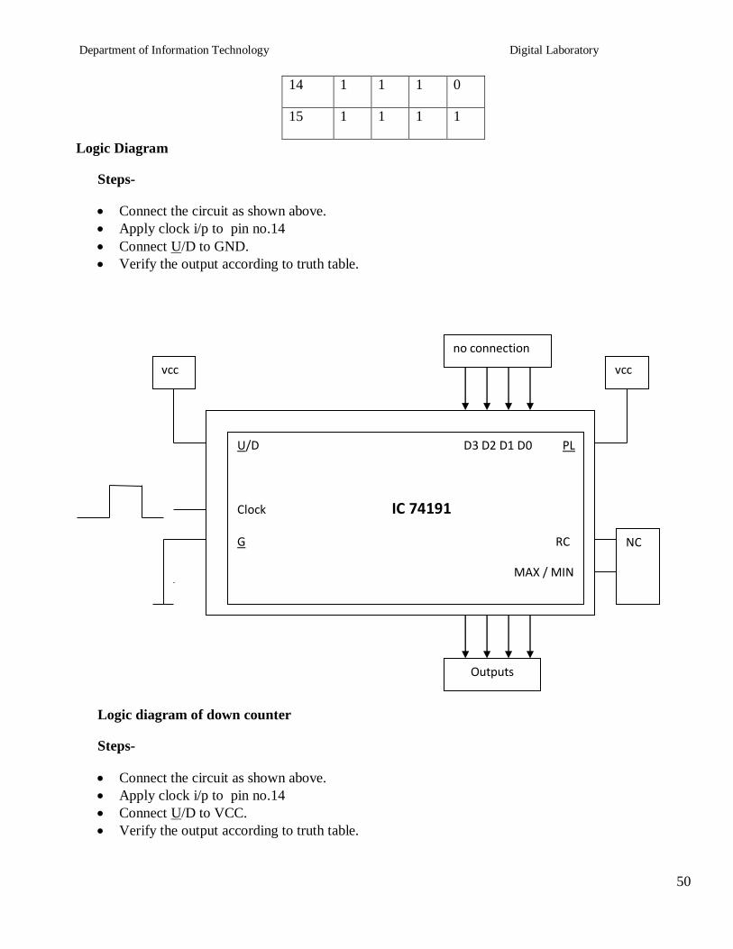
Department of Information Technology Digital Laboratory
50
14 1 1 1 0
15 1 1 1 1
Logic Diagram
Steps-
Connect the circuit as shown above
Apply clock ip to pin no14
Connect UD to GND
Verify the output according to truth table
Logic diagram of down counter
Steps-
Connect the circuit as shown above
Apply clock ip to pin no14
Connect UD to VCC
Verify the output according to truth table
UD D3 D2 D1 D0 PL
Clock IC 74191
G RC
MAX MIN
Q3 Q2 Q1 Q0 TC
vcc
NC
NC
Outputs
no connection
vcc
Department of Information Technology Digital Laboratory
51
With the help of IC74191 we can implement truncated updown counter by using following logic ndash
Connect data input line to particular count you want to load
According to requirement make Truth table
Draw the K-map
Find out Boolean expression
Draw the logic diagram and that is the combinational logic for your count and apply the output of
that circuit to PL
According to requirement we get the UP and down counting
5 Modulus n Counter
Presettable updown counter
Mod 11 counter
Implementation of presetttable mod updown counter using IC- 74LS191
1 Load Data on data lines D0 to D3 (0101)
2 Counter will go through the states from 0101 0110hellip1111 in up counter and 0101 to 0000 in
down counter
Combinational Circuit
CLOCK D3 D2 D1 D0
TC
U D 74191 RC
G PL
Updown Q3 Q2 Q1 Q0 PL
Q3 Q2 Q1 Q0
Preset Count
Department of Information Technology Digital Laboratory
52
3 The logic circuit should be designed in such a way that only when all the outputs are high output
of the reset circuit should be low and the counter should jump to state 5 It should again start
counting from 0101 to 0000
State Table
Down Counter UP Counter
IC 74191 is 4 bit counter Thus it counts 0000 to 1111 different 16 states For MOD11 counter we require
different 11 states so 5 steps must be skipped from 16 states We get MOD11 by presetting counter to
value 5
Assignment Question
Design and Implement MOD 7 MOD 10 and MOD 12 using IC 74191
FAQs
1 What do you mean modulus counter
Counter
state Clock
pulse
Q3 Q2 Q1 Q0
1 0 1 0 1
2 0 1 1 0
3 0 1 1 1
4 1 0 0 0
5 1 0 0 1
6 1 0 1 0
7 1 0 1 1
8 1 1 0 0
9 1 1 0 1
10 1 1 1 1
11 1 1 1 1
Counter state
Clock pulse
FF outputs
Q3 Q2 Q1 Q0
1 0 1 0 1
2 0 1 0 0
3 0 0 1 1
4 0 0 1 0
5 0 0 0 1
6 0 0 0 0
7 0 1 0 1
Department of Information Technology Digital Laboratory
53
It represents the number of possible states of counter
2 How will you use the 7490 IC to design symmetrical divide by 10 frequency counter
The divide by 5 circuit followed by divide by 2 circuit will give symmetrical output
3Where counters are used Give real life example of counter
Modulus n Counter
Binary counter ndash An N stage counter that recycles after 2 Ncount The count proceds in specified binary
sequence Counter Presetable- A counter which can be set to a desired value before the start of the
counting UPDown counter ndash A counter that can count in both up and down direction depending upon a
control input
Department of Information Technology Digital Laboratory
54
Regularity Content Viva-voce Timely
Submission Total
Dated Sign of
Subject
Teacher
2 4 2 2 10
Date of Performance Date of Completion
-------------------------------------------------------------------------------------------------------------------
Assignment No6
------------------------------------------------------------------------------------------------------------------
Title Sequence Generator
------------------------------------------------------------------------------------------------------------------
Objective To understand sequence generator one of the sequential circuit
-------------------------------------------------------------------------------------------------------------------
Problem Statement Design (State Diagram State Table K Map) and implementation of Sequence
Generator using Shift Register IC 74194
-----------------------------------------------------------------------------------------------------------------
Hardware Requirement
i) IC 741947408 (AND-gate) 7432 (OR-gate)
ii) Digital Trainer Kit -1
iii) Patch cords
----------------------------------------------------------------------------------------------------------------
Software Requirement Digital Work 30
------------------------------------------------------------------------------------------------------------------
Theory
Part A Sequence Generator with Flip flop
A sequential circuit which generates a prescribed sequence of bits in synchronism with a clock is referred
to as a sequence generator These pulse trains or sequence of bits can be used to open valves close gates
turn on lights and turn off machines and other variety of jobs
Department of Information Technology Digital Laboratory
55
For the design of sequence generator we first determine the required no of flip flops and the logic circuit
for the next state decoder
No of flip flops required to generate particular sequence can be determined as follows
1) Find the no of 1rsquos in the sequence
2) Find the no of 0rsquos in the sequence
3) Take the maximum out of two
4) If N is the required no of flip flops choose minimum value of lsquonrsquo to satisfy equation given below
Max (0rsquos 1rsquos) le 2n-1
The sequence generator can be classified as
1) sequence generator without bushing
2) sequence generator with bushing
The aim in this experiment is to design a sequence generator to generate a sequence of bit ie 10101
Part B Sequence Generator using Shift Register IC 74194
IC 74194 4 bit bidirectional Shift Register
This bidirectional shift register is designed to incorporate virtually all the features a system designer may
want in a shift register they feature Parallel inputs parallel outputs right shift left shift serialinputs
operating mode control inputsand a direct overriding clear line The register has four distinct modes of
operationsnamely
1 Parallel load
2 Shift right (in the direction QA towards QD)
3 Shift left (in the direction QD towards QA)
4 Inhibit clock (do nothing)
Synchronous parallel loading is accomplished by applying the four bits of data and taking both
mode control inputs S0 and S1High The data is loaded in to the associated flip-flops and appear
at the outputs after positive transition of the clock input During loading serial data flow is
inhibited
Shift right is accomplished synchronously with the rising edge of the clock pulse when S0 is High
and S1 is Low Serial data for this mode is entered at the shift right data input When S0 is Low
and S1 is High data shifts left synchronously and new data is entered at the shift left serial input
Clocking of the flip flop is inhibited when both mode control inputs are LOW
Department of Information Technology Digital Laboratory
56
Mode Control Input Operation
S1 S0
0 0 Clock Inhibit
0 1 Shift right
1 0 Shift Left
1 1 Parallel loading
Function Table of IC 74194
Design
The minimum number of flip-flops N required to generate a sequence of length S is given by S
le 2N ndash 1
In this case S=7 therefore the minimum value of N which may generate in this sequence is 3
However it is not guaranteed to lead to a solution If the given sequence leads to seven distinct
states then only three flip flops are sufficient otherwise we have to increase the number of flip
flops We write the states of circuit as given in table 1 The prescribed sequence is listed under QA
and the sequence listed under QB and QC are the same sequence delayed by one and two clock
pulses respectively From the table we observe that all the states are not distinct which means N=3
is not sufficient Next we assume that N=4 and prepare table 2 The last column gives the required
serial input for getting the desired change of state when a clock pulse is applied This is obtained
by assuming D type flip flop and looking at the QA output For example at the falling edge of first
clock pulse QA=1 The second clock pulse must result in QA=1 which requires its D input to be 1
In the same manner all the entries in column Y are determined
Table 1 State Assignment Table of Sequence Generator (N=3)
Number of Clock
Pulses
Flip Flop Inputs States
QA QB QC
1 1 1 1 7
2 1 1 1 7
3 0 1 1 3
4 1 0 1 5
Department of Information Technology Digital Laboratory
57
5 0 1 0 2
6 1 0 1 5
7 1 1 0 6
Excitation table of D Flip-Flop
Present State Qn Next State Qn+1 Flip-Flop Input D
0 0 0
0 1 1
1 0 0
1 1 1
Table 2State Assignment Table of Sequence Generator (N=4)
Number of Clock
Pulses
Flip Flop Inputs States
Y
Serial ip QA QB QC QD
1 1 1 1 0 14 1
2 1 1 1 1 15 0
3 0 1 1 1 7 1
4 1 0 1 1 11 0
5 0 1 0 1 5 1
6 1 0 1 0 10 1
7 1 1 0 1 13 1
K-Map Simplification
Department of Information Technology Digital Laboratory
58
00 01 11 10
00 X X X X
01 X 1 1 X
11 X 1 0 1
10 X X 0 1
Y= QArsquo + QBrsquo + QCrsquo = QAQBQC
LOGIC DIAGRAM
HARDWARE REQUIREMENTS
Sr no ICs Description Quantity
11 74194 4 bit bidirectional universal shift register 16ktr`
2 7410 3 input NAND Gate 1
Department of Information Technology Digital Laboratory
59
Conclusion In this way sequence generator using JK flip flips amp shift register is designed and
implemented
Enhancements Modifications ndash Sequence generator can also be implemented with shift register instead
of flip flops Use IC 7495 universal shift register IC and try to implement sequence generator
FAQs
1 What is sequential logic circuit
A sequential logic circuit consists of a memory elements in addition to
combinational circuit Its output at any instant of time depends upon
the present input as well as present state of memory element
2 What is meant by delay line
It is used to introduce time delays in digital signals
3 What is meant by following terms
a) Synchronous preset b) Asynchronous preset
c) Synchronous clear d) Asynchronous clear
a)Preset operation is synchronised with the clock
b)Preset operation is independent of the clock
c) clear is performed in synchronous with clock
d) clear is performed independent with clock
4 Is asynchronous counter faster than synchronous counter
In a synchronous counter the time required for change of any state is same and is equal to delay
time of one flip flop where as in asynchronous counter all flip flops are not clocked
simultaneously hence time required is not same
5 What is mean by lockout in counter
In a counter design for a fewer state than the maximum possible state some time it may so happen
that counter enters in unused state and goes from one unused state to another unused state and
never comes to used state
6 What is mean by state table
Department of Information Technology Digital Laboratory
60
It consists of complete information about present state and next state and outputs of a sequential
system
7 What is mean by state diagram
The information available in a state table can be represented as graphically the graphical
representation is known as state diagram
8 What is the advantage of state reduction in the design of sequential circuit
It reduces the number of flip flops
9 What is meant by excitation table
This gives information about what should be the flip flop inputs if outputs are specified before and
after the clock pulse
10 How many flip flops are required to design sequence generator using Counters
max (0rsquoS1rsquoS) in a given sequence lt= 2(N - 1)
Where N = Number of flip flops
11 How many flip flops are required to design sequence generator using shift registers
Slt= 2N - 1
Where N=Number of flip flops
S= Length of sequence
12 What is Lock out condition How it is avoided
When counter enters into one of the invalid state and after application of pulses remains in invalid
states only i e counter gets locked into invalid state amp this is called as lock out Lock out can be
avoided by providing bushing to all the invalid states in such a way that after application of one or
more clock pulses counter will fall into one of the valid state
Department of Information Technology Digital Laboratory
61
Regularity Content Viva-voce Timely
Submission Total
Dated Sign of
Subject
Teacher
2 4 2 2 10
Date of Performance Date of Completion
-------------------------------------------------------------------------------------------------------------------
Assignment No7
------------------------------------------------------------------------------------------------------------------
Title Multiplexer using Data flow modeling and structural modeling
------------------------------------------------------------------------------------------------------------------
Objective To learn data flow modeling style Its uses and different types of declarations with some
different types of circuits Structure of VHDL program is well discussed with this modeling style
-------------------------------------------------------------------------------------------------------------------
Problem Statement 41 multiplexer using data flow amp structural modeling -
----------------------------------------------------------------------------------------------------------------
Hardware Requirement - NA
----------------------------------------------------------------------------------------------------------------
Software Requirement Xilinx
------------------------------------------------------------------------------------------------------------------
Theory
Data flow style-
In this type of design the view of data as flowing from input to output through a design
An operation is defined in terms of a collection of data transformation expressed as concurrent
statement Each of the statement can be activated when any of its input signal changes its value While
these statements describe the behavior of the circuit a lot of information about its structure can be
extracted from the description as well
Data flow modeling has a set of concurrent assignment statements In the data flow level of abstraction we
describe how information is passed in the circuit The built in operators in VHDL are used in expression
such as AND OR XOR NOT etc
Department of Information Technology Digital Laboratory
62
INPUT
Two select lines S1S0
Four data lines D0 D1 D2 D3
OUTPUT
One output line Y
Functional block diagram of 41 Mux
Fig 41 Multiplexer using Data flow modeling
Function table of 41 Mux
Enable S1 S0 A B C D Y
1 X X X X X X 0
0 0 0 A X X X A
0 0 1 X B X X B
0 1 0 X X C X C
0 1 1 X X X D D
Design steps
Click on Xilinx ISE 92i
Create New project from file menu Ensure top level source is HDL
Select family of devices (usually spartan2E or 3)
Department of Information Technology Digital Laboratory
63
Ensure preferred language is VHDL
Click new source which shows you project details device details
and Synthesis and simulator tools
After finishing project create new source by right clicking in project name with VHDL
module
Complete ports name directions and bus Ensure architecture name is behavioral
After that we will get design summary and detailed reports
Close design summary
Create your code with given modeling style
Go to process window and synthesis to check if any error is there in code Check syntax and
view RTL schematic
Create new source to simulate the code
Right click on source name and create test bench waveform with proper name Ensure the
project is same
Click on combinational circuit in initial timing wizard
Select test bench wave in source window Apply inputs to wave diagram Ensure you are in
behavioral simulation
Go to process box Click on Xilinx ISE simulator and simulate the model See results
RTL Schematic
Department of Information Technology Digital Laboratory
64
Timing Diagram
FAQrsquos
1 What are the different kinds of data objects in VHDL code
Ans data object may be any value or number still some signal data objects and bit and bit_vector
types of these are available in VHDL STD_LOGIC and STD_LOGIC_VECTOR types are used
widely in programming
2 What do you mean by signal
Ans signal is a data object represents logic signals or wires in a circuit There are three places in
which signals can be declared in VHDL code in an entity declaration in the declarative section of
architecture and in declarative section of package
3 What are different signal types
Ans BIT BIT_VECTOR STD_LOGIC STD_LOGIC_VECTOR STD_ULOGIC SIGNED
UNSIGNED INTEGER ENUMERATION and BOOLEAN
4 What is an entity
Ans a circuit or sub circuit described with VHDL code is called a design entity
5 Explain structure of an entity
Ans it has two main parts the entity declaration which specifies the input and output signals for
entity and the architecture which gives circuit details
Department of Information Technology Digital Laboratory
65
6 How will you declare a package with component Explain structure
The general form of package declaration is as shown in diagram
PACKAGE package_name IS
[TYPE declarations]
[SIGNAL declarations]
[COMPONENT declarations]
END package_name
Entity
Declaration Architecture
Department of Information Technology Digital Laboratory
66
Regularity Content Viva-voce Timely
Submission Total
Dated Sign of
Subject
Teacher
2 4 2 2 10
Date of Performance Date of Completion
-------------------------------------------------------------------------------------------------------------------
Assignment No8
------------------------------------------------------------------------------------------------------------------
Title Full Adder using Behavioral and Structural modeling
------------------------------------------------------------------------------------------------------------------
Objective To learn structural modeling style Its uses and different types of declarations with some
different types of circuits Structure of VHDL program is well discussed with this modeling style
-------------------------------------------------------------------------------------------------------------------
Problem Statement Full adder using behavioral amp structural modeling
-----------------------------------------------------------------------------------------------------------------
Hardware Requirement - NA
----------------------------------------------------------------------------------------------------------------
Software Requirement Xilinx
------------------------------------------------------------------------------------------------------------------
Theory
Structural style-
A digital electronic system can be described as a module with inputs andor outputs The electrical values
on the outputs are same functions of the values of inputs The example of it is as shown The NAND gate
has 2ips AampB amp an output y Using VHDL terminology we call the NAND2 design entity amp the inputs
amp outputs are called ports 1 way of describing the function of NAND2 is to describe how it is composed
of sub modules AND amp INVERTER Each of the Sub modules is an instance of some entity amp ports of the
instances are connected using signals Structural modeling has a set of interconnected component
Structure can be used to create a very low level description of a circuit or a very high level description
Department of Information Technology Digital Laboratory
67
In a gate level description of a circuit for example components such as basic logic gates amp FFs might be
connected in some logical stricture to create the circuit This is what is often called a net list
Structure of structural modeling
Functional block diagram of Full Adder
architectureNetlistofHalf_Adderis
-- component with locals
componentMyXorport (A_XorB_Xor in BIT
Z_Xor out BIT)
end component
-- component with locals
componentMyAndport (A_AndB_And in BIT
Z_And out BIT)
end component
begin
Xor1 MyXorport map (X Y Sum)
-- instance with actuals
And1 MyAndport map (X Y Cout)
-- instance with actuals
end
Department of Information Technology Digital Laboratory
68
Function table of Full Adder
A B Cin SUM CARRY
0 0 0 0 0
0 0 1 1 0
0 1 0 1 0
0 1 1 0 1
1 0 0 1 0
1 0 1 0 1
1 1 0 0 1
1 1 1 1 1
Sum = Σm(1 2 4 7)
Carry= Σm(3 5 6 7)
Design steps
Click on Xilinx ISE 92i
Create New project from file menu Ensure top level source is HDL
Select family of devices (usually spartan2E or 3)
Ensure preferred language is VHDL
Click new source which shows you project details device details
and Synthesis and simulator tools
After finishing project create new source(full adder) by right clicking in project name with
VHDL module
Complete ports name directions and bus Ensure architecture name is behavioral
After that we will get design summary and detailed reports
Close design summary
Click new source which shows you project details device details
and Synthesis and simulator tools
After finishing project create new source(half adder) by right clicking in project name with
VHDL module
Complete ports name directions and bus Ensure architecture name is behavioral Names
should be same as previous inputs
Department of Information Technology Digital Laboratory
69
After that we will get design summary and detailed reports
Close design summary
Create your code for half adder with given modeling style
After that go to process window Click on design utilities
View HDL instantiation code of half adder
Copy component part of half adder in architecture block of full adder Copy instantiation
template twice after begin as we require two half adders to construct full adder (structural
modeling) Name them differently (eg ha1 or ha2)
Create signals as per the logic Complete code of full adder
Go to process window and synthesis to check if any error is there in code Check syntax and
view RTL schematic
Create new source to simulate the code
Right click on source name and create test bench waveform with proper name Ensure the
project is same
Click on combinational circuit in initial timing wizard
Select test bench wave in source window Apply inputs to wave diagram Ensure you are in
behavioral simulation
Go to process box Click on Xilinx ISE simulator and simulate the model See results
RTL Schematic
Timing Diagram
Department of Information Technology Digital Laboratory
70
INPUT
Three inputs A B Carry (previous)
OUTPUT
Two outputs Sum Carry
FAQrsquos
1 What do you mean by structural style
Ans in this type of code a circuit is described in hierarchical fashion by connecting together sub
circuits
2 Explain IF statement with example
Ans The general form of an IF statement is as follws
IF Sel=rsquo0rsquo THEN
Flt=x1
ELSE
Flt=x2
END IF
Department of Information Technology Digital Laboratory
71
3 Explain declaration and instantiation process in VHDL
Ans first declare a small vhdl code in formal way Eg half adder Define project name is full adder
And simply copy instantiation template in main source code Define how many times you want to
declare this template Give separate names for those
4 What is STD_LOGIC_VECTOR
Ans It is standard data object added to VHDL standard in IEEE 1164 It provides more flexibility
than the Bit type
5 Explain difference between concurrent and sequential statements
Ans Concurrent statements define interconnected processes and blocks that together describe a designrsquos
overall behavior or structure They can be grouped using block sstatement Groups of blocks can also be
partitioned into other blocks At this same level a VHDL component can be connected to define signals
within the blocks
It is a reference to an entity A process can be a single signal assignment statement or a series of
sequential statements (SS) Within a process procedures and functions can partition the sequential
statements
PRACTICE ASSIGNMENTS
1 Implement half adder using data flow modeling
2 Implement Full Adder using behavioral modeling
3 Implement 3 bit magnitude comparator using a 3 bit adder
4 Implement half sub tractor using data flow modeling
5 Write VHDL code for Full Subtractor
Department of Information Technology Digital Laboratory
72
Regularity Content Viva-voce Timely
Submission Total
Dated Sign of
Subject
Teacher
2 4 2 2 10
rsquozaDate of Performance Date of Completion
-------------------------------------------------------------------------------------------------------------------
Assignment No9
------------------------------------------------------------------------------------------------------------------
Title Simulation of 3 bit Connter using Behavioral modeling
------------------------------------------------------------------------------------------------------------------
Objective To learn behavioral modeling style Its uses and different types of declarations with some
different types of circuits Structure of VHDL program is well discussed with this modeling style
-------------------------------------------------------------------------------------------------------------------
Problem Statement 3 bit controlled up down synchronous counter with preset amp clear
-----------------------------------------------------------------------------------------------------------------
Hardware Requirement -NA
----------------------------------------------------------------------------------------------------------------
Software Requirement Xilinx
------------------------------------------------------------------------------------------------------------------
Theory
Behavioral style-
Highest level of abstraction supported in VHDL is called the behavior level of abstraction In it we have
for loop while loop If then else case ampvariable assignment The statements are enclosed in a PROCESS
block amp are executed sequentially
In it circuit is described in terms of its operation overtime
In behavioral description the concept of time may be expressed precisely with actual delays between
related events (such as the propagation delays within gates amp on wires) or it may be simply an ordering of
operation that are expressed sequentially (such as in a functional description of a FF)
Department of Information Technology Digital Laboratory
73
A behavioral design method defines a circuit in terms of text language rather than a schematic of
interconnected symbols
Behavioral design is a technology independent text based design that incorporates high level
functionality amp high level information flow
Structure of Behavioral modeling
Functional block diagram of 3 bit controlled up down synchronous counter with preset amp clear
Function table of 3 bit controlled up down synchronous counter with preset amp clear
Design steps
Click on Xilinx ISE 92i
Create New project from file menu Ensure top level source is HDL
Select family of devices (usually spartan2E or 3)
Ensure preferred language is VHDL
Click new source which shows you project details device details
and Synthesis and simulator tools
After finishing project create new source by right clicking in project name with VHDL
module
Complete ports name directions and bus Ensure architecture name is behavioral
After that we will get design summary and detailed reports
Close design summary
Create your code with given modeling style
Go to process window and synthesis to check if any error is there in code Check syntax
and view RTL schematic Create new source to simulate the code
Department of Information Technology Digital Laboratory
74
Right click on source name and create test bench waveform with proper name Ensure the
project is same
Click on combinational circuit in initial timing wizard
Select test bench wave in source window Apply inputs to wave diagram Ensure you are in
behavioral simulation
Go to process box Click on Xilinx ISE simulator and simulate the model
RTL Schematic
Timing Diagram
INPUT
Clock Preset Clear
OUTPUT
Three output lines
FAQrsquos
1 Explain the structure of behavioral modeling
2 What are the differences between behavioral and structural modeling
Ans Behavioral descriptionof a circuit is the highest level of abstraction in VHDL Here the
circuit is described in terms of it operation with respect to time All operations are in one level of
code The operations are described in a way that the designer of a sequential circuit infers a
register
Structural description on the other hand is a circuit description in terms of its components
it can either create a low level description much like a hierarchy in a block diagram Whenever
you see a component instantiated in a code that code employs structural description of the circuit
The components are connected in the form of a netlist This is for better manageability and
reusability
3 What are the differences between behavioral and data flow modeling
Department of Information Technology Digital Laboratory
75
Ans Behavioral ndash describes how the output is derived from the inputs using structured
statements
Dataflow ndash describes how the data flows from the inputs to the output most often
using NOT AND and OR operations
4 What do you mean by process statement
Ans The process statement begins with the PROCESS keyword followed by a parenthesized list
of signals called the sensitivity list It operates on selected and conditional statements
5 Explain syntax of process statement
Ans BEGIN
Process( sensitivity list)
END process
PRACTICE ASSIGNMENTS
1 Implement 3 bit asynchronous up counter using behavioral modeling
2 Implement 3 bit asynchronous down counter using behavioral modeling
3 Implement 3 bit synchronous down counter using behavioral modeling
End
Department of Information Technology Digital Laboratory
76
Pin Diagrams
7400 Quad 2-Input NAND Gate
7402 Quad 2-Input NOR Gate
7404 Not Gates
7408 Quad 2-Input AND Gates
7432 Quad 2-Input OR Gate
7486 Quad 2-Input Exclusive-OR Gate
Department of Information Technology Digital Laboratory
77
7483 4 bit Binary Adder
7490 Decade and Binary Counters
74138 38 Decoder
Department of Information Technology Digital Laboratory
78
74153 Dual 41 Multiplexer
74191 Synchronous UpDown 4 bit Binary counter with Mode Control
Department of Information Technology Digital Laboratory
79
74194 Universal Shift Register
7476 Dual Master-Slave J-K Flip-Flops
- Part B Sequence Generator using Shift Register IC 74194
-
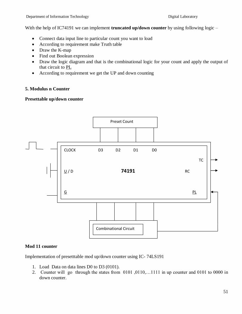
Department of Information Technology Digital Laboratory
51
With the help of IC74191 we can implement truncated updown counter by using following logic ndash
Connect data input line to particular count you want to load
According to requirement make Truth table
Draw the K-map
Find out Boolean expression
Draw the logic diagram and that is the combinational logic for your count and apply the output of
that circuit to PL
According to requirement we get the UP and down counting
5 Modulus n Counter
Presettable updown counter
Mod 11 counter
Implementation of presetttable mod updown counter using IC- 74LS191
1 Load Data on data lines D0 to D3 (0101)
2 Counter will go through the states from 0101 0110hellip1111 in up counter and 0101 to 0000 in
down counter
Combinational Circuit
CLOCK D3 D2 D1 D0
TC
U D 74191 RC
G PL
Updown Q3 Q2 Q1 Q0 PL
Q3 Q2 Q1 Q0
Preset Count
Department of Information Technology Digital Laboratory
52
3 The logic circuit should be designed in such a way that only when all the outputs are high output
of the reset circuit should be low and the counter should jump to state 5 It should again start
counting from 0101 to 0000
State Table
Down Counter UP Counter
IC 74191 is 4 bit counter Thus it counts 0000 to 1111 different 16 states For MOD11 counter we require
different 11 states so 5 steps must be skipped from 16 states We get MOD11 by presetting counter to
value 5
Assignment Question
Design and Implement MOD 7 MOD 10 and MOD 12 using IC 74191
FAQs
1 What do you mean modulus counter
Counter
state Clock
pulse
Q3 Q2 Q1 Q0
1 0 1 0 1
2 0 1 1 0
3 0 1 1 1
4 1 0 0 0
5 1 0 0 1
6 1 0 1 0
7 1 0 1 1
8 1 1 0 0
9 1 1 0 1
10 1 1 1 1
11 1 1 1 1
Counter state
Clock pulse
FF outputs
Q3 Q2 Q1 Q0
1 0 1 0 1
2 0 1 0 0
3 0 0 1 1
4 0 0 1 0
5 0 0 0 1
6 0 0 0 0
7 0 1 0 1
Department of Information Technology Digital Laboratory
53
It represents the number of possible states of counter
2 How will you use the 7490 IC to design symmetrical divide by 10 frequency counter
The divide by 5 circuit followed by divide by 2 circuit will give symmetrical output
3Where counters are used Give real life example of counter
Modulus n Counter
Binary counter ndash An N stage counter that recycles after 2 Ncount The count proceds in specified binary
sequence Counter Presetable- A counter which can be set to a desired value before the start of the
counting UPDown counter ndash A counter that can count in both up and down direction depending upon a
control input
Department of Information Technology Digital Laboratory
54
Regularity Content Viva-voce Timely
Submission Total
Dated Sign of
Subject
Teacher
2 4 2 2 10
Date of Performance Date of Completion
-------------------------------------------------------------------------------------------------------------------
Assignment No6
------------------------------------------------------------------------------------------------------------------
Title Sequence Generator
------------------------------------------------------------------------------------------------------------------
Objective To understand sequence generator one of the sequential circuit
-------------------------------------------------------------------------------------------------------------------
Problem Statement Design (State Diagram State Table K Map) and implementation of Sequence
Generator using Shift Register IC 74194
-----------------------------------------------------------------------------------------------------------------
Hardware Requirement
i) IC 741947408 (AND-gate) 7432 (OR-gate)
ii) Digital Trainer Kit -1
iii) Patch cords
----------------------------------------------------------------------------------------------------------------
Software Requirement Digital Work 30
------------------------------------------------------------------------------------------------------------------
Theory
Part A Sequence Generator with Flip flop
A sequential circuit which generates a prescribed sequence of bits in synchronism with a clock is referred
to as a sequence generator These pulse trains or sequence of bits can be used to open valves close gates
turn on lights and turn off machines and other variety of jobs
Department of Information Technology Digital Laboratory
55
For the design of sequence generator we first determine the required no of flip flops and the logic circuit
for the next state decoder
No of flip flops required to generate particular sequence can be determined as follows
1) Find the no of 1rsquos in the sequence
2) Find the no of 0rsquos in the sequence
3) Take the maximum out of two
4) If N is the required no of flip flops choose minimum value of lsquonrsquo to satisfy equation given below
Max (0rsquos 1rsquos) le 2n-1
The sequence generator can be classified as
1) sequence generator without bushing
2) sequence generator with bushing
The aim in this experiment is to design a sequence generator to generate a sequence of bit ie 10101
Part B Sequence Generator using Shift Register IC 74194
IC 74194 4 bit bidirectional Shift Register
This bidirectional shift register is designed to incorporate virtually all the features a system designer may
want in a shift register they feature Parallel inputs parallel outputs right shift left shift serialinputs
operating mode control inputsand a direct overriding clear line The register has four distinct modes of
operationsnamely
1 Parallel load
2 Shift right (in the direction QA towards QD)
3 Shift left (in the direction QD towards QA)
4 Inhibit clock (do nothing)
Synchronous parallel loading is accomplished by applying the four bits of data and taking both
mode control inputs S0 and S1High The data is loaded in to the associated flip-flops and appear
at the outputs after positive transition of the clock input During loading serial data flow is
inhibited
Shift right is accomplished synchronously with the rising edge of the clock pulse when S0 is High
and S1 is Low Serial data for this mode is entered at the shift right data input When S0 is Low
and S1 is High data shifts left synchronously and new data is entered at the shift left serial input
Clocking of the flip flop is inhibited when both mode control inputs are LOW
Department of Information Technology Digital Laboratory
56
Mode Control Input Operation
S1 S0
0 0 Clock Inhibit
0 1 Shift right
1 0 Shift Left
1 1 Parallel loading
Function Table of IC 74194
Design
The minimum number of flip-flops N required to generate a sequence of length S is given by S
le 2N ndash 1
In this case S=7 therefore the minimum value of N which may generate in this sequence is 3
However it is not guaranteed to lead to a solution If the given sequence leads to seven distinct
states then only three flip flops are sufficient otherwise we have to increase the number of flip
flops We write the states of circuit as given in table 1 The prescribed sequence is listed under QA
and the sequence listed under QB and QC are the same sequence delayed by one and two clock
pulses respectively From the table we observe that all the states are not distinct which means N=3
is not sufficient Next we assume that N=4 and prepare table 2 The last column gives the required
serial input for getting the desired change of state when a clock pulse is applied This is obtained
by assuming D type flip flop and looking at the QA output For example at the falling edge of first
clock pulse QA=1 The second clock pulse must result in QA=1 which requires its D input to be 1
In the same manner all the entries in column Y are determined
Table 1 State Assignment Table of Sequence Generator (N=3)
Number of Clock
Pulses
Flip Flop Inputs States
QA QB QC
1 1 1 1 7
2 1 1 1 7
3 0 1 1 3
4 1 0 1 5
Department of Information Technology Digital Laboratory
57
5 0 1 0 2
6 1 0 1 5
7 1 1 0 6
Excitation table of D Flip-Flop
Present State Qn Next State Qn+1 Flip-Flop Input D
0 0 0
0 1 1
1 0 0
1 1 1
Table 2State Assignment Table of Sequence Generator (N=4)
Number of Clock
Pulses
Flip Flop Inputs States
Y
Serial ip QA QB QC QD
1 1 1 1 0 14 1
2 1 1 1 1 15 0
3 0 1 1 1 7 1
4 1 0 1 1 11 0
5 0 1 0 1 5 1
6 1 0 1 0 10 1
7 1 1 0 1 13 1
K-Map Simplification
Department of Information Technology Digital Laboratory
58
00 01 11 10
00 X X X X
01 X 1 1 X
11 X 1 0 1
10 X X 0 1
Y= QArsquo + QBrsquo + QCrsquo = QAQBQC
LOGIC DIAGRAM
HARDWARE REQUIREMENTS
Sr no ICs Description Quantity
11 74194 4 bit bidirectional universal shift register 16ktr`
2 7410 3 input NAND Gate 1
Department of Information Technology Digital Laboratory
59
Conclusion In this way sequence generator using JK flip flips amp shift register is designed and
implemented
Enhancements Modifications ndash Sequence generator can also be implemented with shift register instead
of flip flops Use IC 7495 universal shift register IC and try to implement sequence generator
FAQs
1 What is sequential logic circuit
A sequential logic circuit consists of a memory elements in addition to
combinational circuit Its output at any instant of time depends upon
the present input as well as present state of memory element
2 What is meant by delay line
It is used to introduce time delays in digital signals
3 What is meant by following terms
a) Synchronous preset b) Asynchronous preset
c) Synchronous clear d) Asynchronous clear
a)Preset operation is synchronised with the clock
b)Preset operation is independent of the clock
c) clear is performed in synchronous with clock
d) clear is performed independent with clock
4 Is asynchronous counter faster than synchronous counter
In a synchronous counter the time required for change of any state is same and is equal to delay
time of one flip flop where as in asynchronous counter all flip flops are not clocked
simultaneously hence time required is not same
5 What is mean by lockout in counter
In a counter design for a fewer state than the maximum possible state some time it may so happen
that counter enters in unused state and goes from one unused state to another unused state and
never comes to used state
6 What is mean by state table
Department of Information Technology Digital Laboratory
60
It consists of complete information about present state and next state and outputs of a sequential
system
7 What is mean by state diagram
The information available in a state table can be represented as graphically the graphical
representation is known as state diagram
8 What is the advantage of state reduction in the design of sequential circuit
It reduces the number of flip flops
9 What is meant by excitation table
This gives information about what should be the flip flop inputs if outputs are specified before and
after the clock pulse
10 How many flip flops are required to design sequence generator using Counters
max (0rsquoS1rsquoS) in a given sequence lt= 2(N - 1)
Where N = Number of flip flops
11 How many flip flops are required to design sequence generator using shift registers
Slt= 2N - 1
Where N=Number of flip flops
S= Length of sequence
12 What is Lock out condition How it is avoided
When counter enters into one of the invalid state and after application of pulses remains in invalid
states only i e counter gets locked into invalid state amp this is called as lock out Lock out can be
avoided by providing bushing to all the invalid states in such a way that after application of one or
more clock pulses counter will fall into one of the valid state
Department of Information Technology Digital Laboratory
61
Regularity Content Viva-voce Timely
Submission Total
Dated Sign of
Subject
Teacher
2 4 2 2 10
Date of Performance Date of Completion
-------------------------------------------------------------------------------------------------------------------
Assignment No7
------------------------------------------------------------------------------------------------------------------
Title Multiplexer using Data flow modeling and structural modeling
------------------------------------------------------------------------------------------------------------------
Objective To learn data flow modeling style Its uses and different types of declarations with some
different types of circuits Structure of VHDL program is well discussed with this modeling style
-------------------------------------------------------------------------------------------------------------------
Problem Statement 41 multiplexer using data flow amp structural modeling -
----------------------------------------------------------------------------------------------------------------
Hardware Requirement - NA
----------------------------------------------------------------------------------------------------------------
Software Requirement Xilinx
------------------------------------------------------------------------------------------------------------------
Theory
Data flow style-
In this type of design the view of data as flowing from input to output through a design
An operation is defined in terms of a collection of data transformation expressed as concurrent
statement Each of the statement can be activated when any of its input signal changes its value While
these statements describe the behavior of the circuit a lot of information about its structure can be
extracted from the description as well
Data flow modeling has a set of concurrent assignment statements In the data flow level of abstraction we
describe how information is passed in the circuit The built in operators in VHDL are used in expression
such as AND OR XOR NOT etc
Department of Information Technology Digital Laboratory
62
INPUT
Two select lines S1S0
Four data lines D0 D1 D2 D3
OUTPUT
One output line Y
Functional block diagram of 41 Mux
Fig 41 Multiplexer using Data flow modeling
Function table of 41 Mux
Enable S1 S0 A B C D Y
1 X X X X X X 0
0 0 0 A X X X A
0 0 1 X B X X B
0 1 0 X X C X C
0 1 1 X X X D D
Design steps
Click on Xilinx ISE 92i
Create New project from file menu Ensure top level source is HDL
Select family of devices (usually spartan2E or 3)
Department of Information Technology Digital Laboratory
63
Ensure preferred language is VHDL
Click new source which shows you project details device details
and Synthesis and simulator tools
After finishing project create new source by right clicking in project name with VHDL
module
Complete ports name directions and bus Ensure architecture name is behavioral
After that we will get design summary and detailed reports
Close design summary
Create your code with given modeling style
Go to process window and synthesis to check if any error is there in code Check syntax and
view RTL schematic
Create new source to simulate the code
Right click on source name and create test bench waveform with proper name Ensure the
project is same
Click on combinational circuit in initial timing wizard
Select test bench wave in source window Apply inputs to wave diagram Ensure you are in
behavioral simulation
Go to process box Click on Xilinx ISE simulator and simulate the model See results
RTL Schematic
Department of Information Technology Digital Laboratory
64
Timing Diagram
FAQrsquos
1 What are the different kinds of data objects in VHDL code
Ans data object may be any value or number still some signal data objects and bit and bit_vector
types of these are available in VHDL STD_LOGIC and STD_LOGIC_VECTOR types are used
widely in programming
2 What do you mean by signal
Ans signal is a data object represents logic signals or wires in a circuit There are three places in
which signals can be declared in VHDL code in an entity declaration in the declarative section of
architecture and in declarative section of package
3 What are different signal types
Ans BIT BIT_VECTOR STD_LOGIC STD_LOGIC_VECTOR STD_ULOGIC SIGNED
UNSIGNED INTEGER ENUMERATION and BOOLEAN
4 What is an entity
Ans a circuit or sub circuit described with VHDL code is called a design entity
5 Explain structure of an entity
Ans it has two main parts the entity declaration which specifies the input and output signals for
entity and the architecture which gives circuit details
Department of Information Technology Digital Laboratory
65
6 How will you declare a package with component Explain structure
The general form of package declaration is as shown in diagram
PACKAGE package_name IS
[TYPE declarations]
[SIGNAL declarations]
[COMPONENT declarations]
END package_name
Entity
Declaration Architecture
Department of Information Technology Digital Laboratory
66
Regularity Content Viva-voce Timely
Submission Total
Dated Sign of
Subject
Teacher
2 4 2 2 10
Date of Performance Date of Completion
-------------------------------------------------------------------------------------------------------------------
Assignment No8
------------------------------------------------------------------------------------------------------------------
Title Full Adder using Behavioral and Structural modeling
------------------------------------------------------------------------------------------------------------------
Objective To learn structural modeling style Its uses and different types of declarations with some
different types of circuits Structure of VHDL program is well discussed with this modeling style
-------------------------------------------------------------------------------------------------------------------
Problem Statement Full adder using behavioral amp structural modeling
-----------------------------------------------------------------------------------------------------------------
Hardware Requirement - NA
----------------------------------------------------------------------------------------------------------------
Software Requirement Xilinx
------------------------------------------------------------------------------------------------------------------
Theory
Structural style-
A digital electronic system can be described as a module with inputs andor outputs The electrical values
on the outputs are same functions of the values of inputs The example of it is as shown The NAND gate
has 2ips AampB amp an output y Using VHDL terminology we call the NAND2 design entity amp the inputs
amp outputs are called ports 1 way of describing the function of NAND2 is to describe how it is composed
of sub modules AND amp INVERTER Each of the Sub modules is an instance of some entity amp ports of the
instances are connected using signals Structural modeling has a set of interconnected component
Structure can be used to create a very low level description of a circuit or a very high level description
Department of Information Technology Digital Laboratory
67
In a gate level description of a circuit for example components such as basic logic gates amp FFs might be
connected in some logical stricture to create the circuit This is what is often called a net list
Structure of structural modeling
Functional block diagram of Full Adder
architectureNetlistofHalf_Adderis
-- component with locals
componentMyXorport (A_XorB_Xor in BIT
Z_Xor out BIT)
end component
-- component with locals
componentMyAndport (A_AndB_And in BIT
Z_And out BIT)
end component
begin
Xor1 MyXorport map (X Y Sum)
-- instance with actuals
And1 MyAndport map (X Y Cout)
-- instance with actuals
end
Department of Information Technology Digital Laboratory
68
Function table of Full Adder
A B Cin SUM CARRY
0 0 0 0 0
0 0 1 1 0
0 1 0 1 0
0 1 1 0 1
1 0 0 1 0
1 0 1 0 1
1 1 0 0 1
1 1 1 1 1
Sum = Σm(1 2 4 7)
Carry= Σm(3 5 6 7)
Design steps
Click on Xilinx ISE 92i
Create New project from file menu Ensure top level source is HDL
Select family of devices (usually spartan2E or 3)
Ensure preferred language is VHDL
Click new source which shows you project details device details
and Synthesis and simulator tools
After finishing project create new source(full adder) by right clicking in project name with
VHDL module
Complete ports name directions and bus Ensure architecture name is behavioral
After that we will get design summary and detailed reports
Close design summary
Click new source which shows you project details device details
and Synthesis and simulator tools
After finishing project create new source(half adder) by right clicking in project name with
VHDL module
Complete ports name directions and bus Ensure architecture name is behavioral Names
should be same as previous inputs
Department of Information Technology Digital Laboratory
69
After that we will get design summary and detailed reports
Close design summary
Create your code for half adder with given modeling style
After that go to process window Click on design utilities
View HDL instantiation code of half adder
Copy component part of half adder in architecture block of full adder Copy instantiation
template twice after begin as we require two half adders to construct full adder (structural
modeling) Name them differently (eg ha1 or ha2)
Create signals as per the logic Complete code of full adder
Go to process window and synthesis to check if any error is there in code Check syntax and
view RTL schematic
Create new source to simulate the code
Right click on source name and create test bench waveform with proper name Ensure the
project is same
Click on combinational circuit in initial timing wizard
Select test bench wave in source window Apply inputs to wave diagram Ensure you are in
behavioral simulation
Go to process box Click on Xilinx ISE simulator and simulate the model See results
RTL Schematic
Timing Diagram
Department of Information Technology Digital Laboratory
70
INPUT
Three inputs A B Carry (previous)
OUTPUT
Two outputs Sum Carry
FAQrsquos
1 What do you mean by structural style
Ans in this type of code a circuit is described in hierarchical fashion by connecting together sub
circuits
2 Explain IF statement with example
Ans The general form of an IF statement is as follws
IF Sel=rsquo0rsquo THEN
Flt=x1
ELSE
Flt=x2
END IF
Department of Information Technology Digital Laboratory
71
3 Explain declaration and instantiation process in VHDL
Ans first declare a small vhdl code in formal way Eg half adder Define project name is full adder
And simply copy instantiation template in main source code Define how many times you want to
declare this template Give separate names for those
4 What is STD_LOGIC_VECTOR
Ans It is standard data object added to VHDL standard in IEEE 1164 It provides more flexibility
than the Bit type
5 Explain difference between concurrent and sequential statements
Ans Concurrent statements define interconnected processes and blocks that together describe a designrsquos
overall behavior or structure They can be grouped using block sstatement Groups of blocks can also be
partitioned into other blocks At this same level a VHDL component can be connected to define signals
within the blocks
It is a reference to an entity A process can be a single signal assignment statement or a series of
sequential statements (SS) Within a process procedures and functions can partition the sequential
statements
PRACTICE ASSIGNMENTS
1 Implement half adder using data flow modeling
2 Implement Full Adder using behavioral modeling
3 Implement 3 bit magnitude comparator using a 3 bit adder
4 Implement half sub tractor using data flow modeling
5 Write VHDL code for Full Subtractor
Department of Information Technology Digital Laboratory
72
Regularity Content Viva-voce Timely
Submission Total
Dated Sign of
Subject
Teacher
2 4 2 2 10
rsquozaDate of Performance Date of Completion
-------------------------------------------------------------------------------------------------------------------
Assignment No9
------------------------------------------------------------------------------------------------------------------
Title Simulation of 3 bit Connter using Behavioral modeling
------------------------------------------------------------------------------------------------------------------
Objective To learn behavioral modeling style Its uses and different types of declarations with some
different types of circuits Structure of VHDL program is well discussed with this modeling style
-------------------------------------------------------------------------------------------------------------------
Problem Statement 3 bit controlled up down synchronous counter with preset amp clear
-----------------------------------------------------------------------------------------------------------------
Hardware Requirement -NA
----------------------------------------------------------------------------------------------------------------
Software Requirement Xilinx
------------------------------------------------------------------------------------------------------------------
Theory
Behavioral style-
Highest level of abstraction supported in VHDL is called the behavior level of abstraction In it we have
for loop while loop If then else case ampvariable assignment The statements are enclosed in a PROCESS
block amp are executed sequentially
In it circuit is described in terms of its operation overtime
In behavioral description the concept of time may be expressed precisely with actual delays between
related events (such as the propagation delays within gates amp on wires) or it may be simply an ordering of
operation that are expressed sequentially (such as in a functional description of a FF)
Department of Information Technology Digital Laboratory
73
A behavioral design method defines a circuit in terms of text language rather than a schematic of
interconnected symbols
Behavioral design is a technology independent text based design that incorporates high level
functionality amp high level information flow
Structure of Behavioral modeling
Functional block diagram of 3 bit controlled up down synchronous counter with preset amp clear
Function table of 3 bit controlled up down synchronous counter with preset amp clear
Design steps
Click on Xilinx ISE 92i
Create New project from file menu Ensure top level source is HDL
Select family of devices (usually spartan2E or 3)
Ensure preferred language is VHDL
Click new source which shows you project details device details
and Synthesis and simulator tools
After finishing project create new source by right clicking in project name with VHDL
module
Complete ports name directions and bus Ensure architecture name is behavioral
After that we will get design summary and detailed reports
Close design summary
Create your code with given modeling style
Go to process window and synthesis to check if any error is there in code Check syntax
and view RTL schematic Create new source to simulate the code
Department of Information Technology Digital Laboratory
74
Right click on source name and create test bench waveform with proper name Ensure the
project is same
Click on combinational circuit in initial timing wizard
Select test bench wave in source window Apply inputs to wave diagram Ensure you are in
behavioral simulation
Go to process box Click on Xilinx ISE simulator and simulate the model
RTL Schematic
Timing Diagram
INPUT
Clock Preset Clear
OUTPUT
Three output lines
FAQrsquos
1 Explain the structure of behavioral modeling
2 What are the differences between behavioral and structural modeling
Ans Behavioral descriptionof a circuit is the highest level of abstraction in VHDL Here the
circuit is described in terms of it operation with respect to time All operations are in one level of
code The operations are described in a way that the designer of a sequential circuit infers a
register
Structural description on the other hand is a circuit description in terms of its components
it can either create a low level description much like a hierarchy in a block diagram Whenever
you see a component instantiated in a code that code employs structural description of the circuit
The components are connected in the form of a netlist This is for better manageability and
reusability
3 What are the differences between behavioral and data flow modeling
Department of Information Technology Digital Laboratory
75
Ans Behavioral ndash describes how the output is derived from the inputs using structured
statements
Dataflow ndash describes how the data flows from the inputs to the output most often
using NOT AND and OR operations
4 What do you mean by process statement
Ans The process statement begins with the PROCESS keyword followed by a parenthesized list
of signals called the sensitivity list It operates on selected and conditional statements
5 Explain syntax of process statement
Ans BEGIN
Process( sensitivity list)
END process
PRACTICE ASSIGNMENTS
1 Implement 3 bit asynchronous up counter using behavioral modeling
2 Implement 3 bit asynchronous down counter using behavioral modeling
3 Implement 3 bit synchronous down counter using behavioral modeling
End
Department of Information Technology Digital Laboratory
76
Pin Diagrams
7400 Quad 2-Input NAND Gate
7402 Quad 2-Input NOR Gate
7404 Not Gates
7408 Quad 2-Input AND Gates
7432 Quad 2-Input OR Gate
7486 Quad 2-Input Exclusive-OR Gate
Department of Information Technology Digital Laboratory
77
7483 4 bit Binary Adder
7490 Decade and Binary Counters
74138 38 Decoder
Department of Information Technology Digital Laboratory
78
74153 Dual 41 Multiplexer
74191 Synchronous UpDown 4 bit Binary counter with Mode Control
Department of Information Technology Digital Laboratory
79
74194 Universal Shift Register
7476 Dual Master-Slave J-K Flip-Flops
- Part B Sequence Generator using Shift Register IC 74194
-
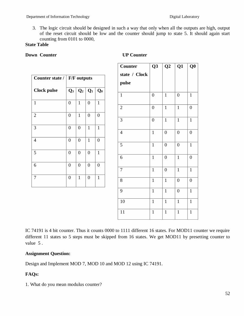
Department of Information Technology Digital Laboratory
55
For the design of sequence generator we first determine the required no of flip flops and the logic circuit
for the next state decoder
No of flip flops required to generate particular sequence can be determined as follows
1) Find the no of 1rsquos in the sequence
2) Find the no of 0rsquos in the sequence
3) Take the maximum out of two
4) If N is the required no of flip flops choose minimum value of lsquonrsquo to satisfy equation given below
Max (0rsquos 1rsquos) le 2n-1
The sequence generator can be classified as
1) sequence generator without bushing
2) sequence generator with bushing
The aim in this experiment is to design a sequence generator to generate a sequence of bit ie 10101
Part B Sequence Generator using Shift Register IC 74194
IC 74194 4 bit bidirectional Shift Register
This bidirectional shift register is designed to incorporate virtually all the features a system designer may
want in a shift register they feature Parallel inputs parallel outputs right shift left shift serialinputs
operating mode control inputsand a direct overriding clear line The register has four distinct modes of
operationsnamely
1 Parallel load
2 Shift right (in the direction QA towards QD)
3 Shift left (in the direction QD towards QA)
4 Inhibit clock (do nothing)
Synchronous parallel loading is accomplished by applying the four bits of data and taking both
mode control inputs S0 and S1High The data is loaded in to the associated flip-flops and appear
at the outputs after positive transition of the clock input During loading serial data flow is
inhibited
Shift right is accomplished synchronously with the rising edge of the clock pulse when S0 is High
and S1 is Low Serial data for this mode is entered at the shift right data input When S0 is Low
and S1 is High data shifts left synchronously and new data is entered at the shift left serial input
Clocking of the flip flop is inhibited when both mode control inputs are LOW
Department of Information Technology Digital Laboratory
56
Mode Control Input Operation
S1 S0
0 0 Clock Inhibit
0 1 Shift right
1 0 Shift Left
1 1 Parallel loading
Function Table of IC 74194
Design
The minimum number of flip-flops N required to generate a sequence of length S is given by S
le 2N ndash 1
In this case S=7 therefore the minimum value of N which may generate in this sequence is 3
However it is not guaranteed to lead to a solution If the given sequence leads to seven distinct
states then only three flip flops are sufficient otherwise we have to increase the number of flip
flops We write the states of circuit as given in table 1 The prescribed sequence is listed under QA
and the sequence listed under QB and QC are the same sequence delayed by one and two clock
pulses respectively From the table we observe that all the states are not distinct which means N=3
is not sufficient Next we assume that N=4 and prepare table 2 The last column gives the required
serial input for getting the desired change of state when a clock pulse is applied This is obtained
by assuming D type flip flop and looking at the QA output For example at the falling edge of first
clock pulse QA=1 The second clock pulse must result in QA=1 which requires its D input to be 1
In the same manner all the entries in column Y are determined
Table 1 State Assignment Table of Sequence Generator (N=3)
Number of Clock
Pulses
Flip Flop Inputs States
QA QB QC
1 1 1 1 7
2 1 1 1 7
3 0 1 1 3
4 1 0 1 5
Department of Information Technology Digital Laboratory
57
5 0 1 0 2
6 1 0 1 5
7 1 1 0 6
Excitation table of D Flip-Flop
Present State Qn Next State Qn+1 Flip-Flop Input D
0 0 0
0 1 1
1 0 0
1 1 1
Table 2State Assignment Table of Sequence Generator (N=4)
Number of Clock
Pulses
Flip Flop Inputs States
Y
Serial ip QA QB QC QD
1 1 1 1 0 14 1
2 1 1 1 1 15 0
3 0 1 1 1 7 1
4 1 0 1 1 11 0
5 0 1 0 1 5 1
6 1 0 1 0 10 1
7 1 1 0 1 13 1
K-Map Simplification
Department of Information Technology Digital Laboratory
58
00 01 11 10
00 X X X X
01 X 1 1 X
11 X 1 0 1
10 X X 0 1
Y= QArsquo + QBrsquo + QCrsquo = QAQBQC
LOGIC DIAGRAM
HARDWARE REQUIREMENTS
Sr no ICs Description Quantity
11 74194 4 bit bidirectional universal shift register 16ktr`
2 7410 3 input NAND Gate 1
Department of Information Technology Digital Laboratory
59
Conclusion In this way sequence generator using JK flip flips amp shift register is designed and
implemented
Enhancements Modifications ndash Sequence generator can also be implemented with shift register instead
of flip flops Use IC 7495 universal shift register IC and try to implement sequence generator
FAQs
1 What is sequential logic circuit
A sequential logic circuit consists of a memory elements in addition to
combinational circuit Its output at any instant of time depends upon
the present input as well as present state of memory element
2 What is meant by delay line
It is used to introduce time delays in digital signals
3 What is meant by following terms
a) Synchronous preset b) Asynchronous preset
c) Synchronous clear d) Asynchronous clear
a)Preset operation is synchronised with the clock
b)Preset operation is independent of the clock
c) clear is performed in synchronous with clock
d) clear is performed independent with clock
4 Is asynchronous counter faster than synchronous counter
In a synchronous counter the time required for change of any state is same and is equal to delay
time of one flip flop where as in asynchronous counter all flip flops are not clocked
simultaneously hence time required is not same
5 What is mean by lockout in counter
In a counter design for a fewer state than the maximum possible state some time it may so happen
that counter enters in unused state and goes from one unused state to another unused state and
never comes to used state
6 What is mean by state table
Department of Information Technology Digital Laboratory
60
It consists of complete information about present state and next state and outputs of a sequential
system
7 What is mean by state diagram
The information available in a state table can be represented as graphically the graphical
representation is known as state diagram
8 What is the advantage of state reduction in the design of sequential circuit
It reduces the number of flip flops
9 What is meant by excitation table
This gives information about what should be the flip flop inputs if outputs are specified before and
after the clock pulse
10 How many flip flops are required to design sequence generator using Counters
max (0rsquoS1rsquoS) in a given sequence lt= 2(N - 1)
Where N = Number of flip flops
11 How many flip flops are required to design sequence generator using shift registers
Slt= 2N - 1
Where N=Number of flip flops
S= Length of sequence
12 What is Lock out condition How it is avoided
When counter enters into one of the invalid state and after application of pulses remains in invalid
states only i e counter gets locked into invalid state amp this is called as lock out Lock out can be
avoided by providing bushing to all the invalid states in such a way that after application of one or
more clock pulses counter will fall into one of the valid state
Department of Information Technology Digital Laboratory
61
Regularity Content Viva-voce Timely
Submission Total
Dated Sign of
Subject
Teacher
2 4 2 2 10
Date of Performance Date of Completion
-------------------------------------------------------------------------------------------------------------------
Assignment No7
------------------------------------------------------------------------------------------------------------------
Title Multiplexer using Data flow modeling and structural modeling
------------------------------------------------------------------------------------------------------------------
Objective To learn data flow modeling style Its uses and different types of declarations with some
different types of circuits Structure of VHDL program is well discussed with this modeling style
-------------------------------------------------------------------------------------------------------------------
Problem Statement 41 multiplexer using data flow amp structural modeling -
----------------------------------------------------------------------------------------------------------------
Hardware Requirement - NA
----------------------------------------------------------------------------------------------------------------
Software Requirement Xilinx
------------------------------------------------------------------------------------------------------------------
Theory
Data flow style-
In this type of design the view of data as flowing from input to output through a design
An operation is defined in terms of a collection of data transformation expressed as concurrent
statement Each of the statement can be activated when any of its input signal changes its value While
these statements describe the behavior of the circuit a lot of information about its structure can be
extracted from the description as well
Data flow modeling has a set of concurrent assignment statements In the data flow level of abstraction we
describe how information is passed in the circuit The built in operators in VHDL are used in expression
such as AND OR XOR NOT etc
Department of Information Technology Digital Laboratory
62
INPUT
Two select lines S1S0
Four data lines D0 D1 D2 D3
OUTPUT
One output line Y
Functional block diagram of 41 Mux
Fig 41 Multiplexer using Data flow modeling
Function table of 41 Mux
Enable S1 S0 A B C D Y
1 X X X X X X 0
0 0 0 A X X X A
0 0 1 X B X X B
0 1 0 X X C X C
0 1 1 X X X D D
Design steps
Click on Xilinx ISE 92i
Create New project from file menu Ensure top level source is HDL
Select family of devices (usually spartan2E or 3)
Department of Information Technology Digital Laboratory
63
Ensure preferred language is VHDL
Click new source which shows you project details device details
and Synthesis and simulator tools
After finishing project create new source by right clicking in project name with VHDL
module
Complete ports name directions and bus Ensure architecture name is behavioral
After that we will get design summary and detailed reports
Close design summary
Create your code with given modeling style
Go to process window and synthesis to check if any error is there in code Check syntax and
view RTL schematic
Create new source to simulate the code
Right click on source name and create test bench waveform with proper name Ensure the
project is same
Click on combinational circuit in initial timing wizard
Select test bench wave in source window Apply inputs to wave diagram Ensure you are in
behavioral simulation
Go to process box Click on Xilinx ISE simulator and simulate the model See results
RTL Schematic
Department of Information Technology Digital Laboratory
64
Timing Diagram
FAQrsquos
1 What are the different kinds of data objects in VHDL code
Ans data object may be any value or number still some signal data objects and bit and bit_vector
types of these are available in VHDL STD_LOGIC and STD_LOGIC_VECTOR types are used
widely in programming
2 What do you mean by signal
Ans signal is a data object represents logic signals or wires in a circuit There are three places in
which signals can be declared in VHDL code in an entity declaration in the declarative section of
architecture and in declarative section of package
3 What are different signal types
Ans BIT BIT_VECTOR STD_LOGIC STD_LOGIC_VECTOR STD_ULOGIC SIGNED
UNSIGNED INTEGER ENUMERATION and BOOLEAN
4 What is an entity
Ans a circuit or sub circuit described with VHDL code is called a design entity
5 Explain structure of an entity
Ans it has two main parts the entity declaration which specifies the input and output signals for
entity and the architecture which gives circuit details
Department of Information Technology Digital Laboratory
65
6 How will you declare a package with component Explain structure
The general form of package declaration is as shown in diagram
PACKAGE package_name IS
[TYPE declarations]
[SIGNAL declarations]
[COMPONENT declarations]
END package_name
Entity
Declaration Architecture
Department of Information Technology Digital Laboratory
66
Regularity Content Viva-voce Timely
Submission Total
Dated Sign of
Subject
Teacher
2 4 2 2 10
Date of Performance Date of Completion
-------------------------------------------------------------------------------------------------------------------
Assignment No8
------------------------------------------------------------------------------------------------------------------
Title Full Adder using Behavioral and Structural modeling
------------------------------------------------------------------------------------------------------------------
Objective To learn structural modeling style Its uses and different types of declarations with some
different types of circuits Structure of VHDL program is well discussed with this modeling style
-------------------------------------------------------------------------------------------------------------------
Problem Statement Full adder using behavioral amp structural modeling
-----------------------------------------------------------------------------------------------------------------
Hardware Requirement - NA
----------------------------------------------------------------------------------------------------------------
Software Requirement Xilinx
------------------------------------------------------------------------------------------------------------------
Theory
Structural style-
A digital electronic system can be described as a module with inputs andor outputs The electrical values
on the outputs are same functions of the values of inputs The example of it is as shown The NAND gate
has 2ips AampB amp an output y Using VHDL terminology we call the NAND2 design entity amp the inputs
amp outputs are called ports 1 way of describing the function of NAND2 is to describe how it is composed
of sub modules AND amp INVERTER Each of the Sub modules is an instance of some entity amp ports of the
instances are connected using signals Structural modeling has a set of interconnected component
Structure can be used to create a very low level description of a circuit or a very high level description
Department of Information Technology Digital Laboratory
67
In a gate level description of a circuit for example components such as basic logic gates amp FFs might be
connected in some logical stricture to create the circuit This is what is often called a net list
Structure of structural modeling
Functional block diagram of Full Adder
architectureNetlistofHalf_Adderis
-- component with locals
componentMyXorport (A_XorB_Xor in BIT
Z_Xor out BIT)
end component
-- component with locals
componentMyAndport (A_AndB_And in BIT
Z_And out BIT)
end component
begin
Xor1 MyXorport map (X Y Sum)
-- instance with actuals
And1 MyAndport map (X Y Cout)
-- instance with actuals
end
Department of Information Technology Digital Laboratory
68
Function table of Full Adder
A B Cin SUM CARRY
0 0 0 0 0
0 0 1 1 0
0 1 0 1 0
0 1 1 0 1
1 0 0 1 0
1 0 1 0 1
1 1 0 0 1
1 1 1 1 1
Sum = Σm(1 2 4 7)
Carry= Σm(3 5 6 7)
Design steps
Click on Xilinx ISE 92i
Create New project from file menu Ensure top level source is HDL
Select family of devices (usually spartan2E or 3)
Ensure preferred language is VHDL
Click new source which shows you project details device details
and Synthesis and simulator tools
After finishing project create new source(full adder) by right clicking in project name with
VHDL module
Complete ports name directions and bus Ensure architecture name is behavioral
After that we will get design summary and detailed reports
Close design summary
Click new source which shows you project details device details
and Synthesis and simulator tools
After finishing project create new source(half adder) by right clicking in project name with
VHDL module
Complete ports name directions and bus Ensure architecture name is behavioral Names
should be same as previous inputs
Department of Information Technology Digital Laboratory
69
After that we will get design summary and detailed reports
Close design summary
Create your code for half adder with given modeling style
After that go to process window Click on design utilities
View HDL instantiation code of half adder
Copy component part of half adder in architecture block of full adder Copy instantiation
template twice after begin as we require two half adders to construct full adder (structural
modeling) Name them differently (eg ha1 or ha2)
Create signals as per the logic Complete code of full adder
Go to process window and synthesis to check if any error is there in code Check syntax and
view RTL schematic
Create new source to simulate the code
Right click on source name and create test bench waveform with proper name Ensure the
project is same
Click on combinational circuit in initial timing wizard
Select test bench wave in source window Apply inputs to wave diagram Ensure you are in
behavioral simulation
Go to process box Click on Xilinx ISE simulator and simulate the model See results
RTL Schematic
Timing Diagram
Department of Information Technology Digital Laboratory
70
INPUT
Three inputs A B Carry (previous)
OUTPUT
Two outputs Sum Carry
FAQrsquos
1 What do you mean by structural style
Ans in this type of code a circuit is described in hierarchical fashion by connecting together sub
circuits
2 Explain IF statement with example
Ans The general form of an IF statement is as follws
IF Sel=rsquo0rsquo THEN
Flt=x1
ELSE
Flt=x2
END IF
Department of Information Technology Digital Laboratory
71
3 Explain declaration and instantiation process in VHDL
Ans first declare a small vhdl code in formal way Eg half adder Define project name is full adder
And simply copy instantiation template in main source code Define how many times you want to
declare this template Give separate names for those
4 What is STD_LOGIC_VECTOR
Ans It is standard data object added to VHDL standard in IEEE 1164 It provides more flexibility
than the Bit type
5 Explain difference between concurrent and sequential statements
Ans Concurrent statements define interconnected processes and blocks that together describe a designrsquos
overall behavior or structure They can be grouped using block sstatement Groups of blocks can also be
partitioned into other blocks At this same level a VHDL component can be connected to define signals
within the blocks
It is a reference to an entity A process can be a single signal assignment statement or a series of
sequential statements (SS) Within a process procedures and functions can partition the sequential
statements
PRACTICE ASSIGNMENTS
1 Implement half adder using data flow modeling
2 Implement Full Adder using behavioral modeling
3 Implement 3 bit magnitude comparator using a 3 bit adder
4 Implement half sub tractor using data flow modeling
5 Write VHDL code for Full Subtractor
Department of Information Technology Digital Laboratory
72
Regularity Content Viva-voce Timely
Submission Total
Dated Sign of
Subject
Teacher
2 4 2 2 10
rsquozaDate of Performance Date of Completion
-------------------------------------------------------------------------------------------------------------------
Assignment No9
------------------------------------------------------------------------------------------------------------------
Title Simulation of 3 bit Connter using Behavioral modeling
------------------------------------------------------------------------------------------------------------------
Objective To learn behavioral modeling style Its uses and different types of declarations with some
different types of circuits Structure of VHDL program is well discussed with this modeling style
-------------------------------------------------------------------------------------------------------------------
Problem Statement 3 bit controlled up down synchronous counter with preset amp clear
-----------------------------------------------------------------------------------------------------------------
Hardware Requirement -NA
----------------------------------------------------------------------------------------------------------------
Software Requirement Xilinx
------------------------------------------------------------------------------------------------------------------
Theory
Behavioral style-
Highest level of abstraction supported in VHDL is called the behavior level of abstraction In it we have
for loop while loop If then else case ampvariable assignment The statements are enclosed in a PROCESS
block amp are executed sequentially
In it circuit is described in terms of its operation overtime
In behavioral description the concept of time may be expressed precisely with actual delays between
related events (such as the propagation delays within gates amp on wires) or it may be simply an ordering of
operation that are expressed sequentially (such as in a functional description of a FF)
Department of Information Technology Digital Laboratory
73
A behavioral design method defines a circuit in terms of text language rather than a schematic of
interconnected symbols
Behavioral design is a technology independent text based design that incorporates high level
functionality amp high level information flow
Structure of Behavioral modeling
Functional block diagram of 3 bit controlled up down synchronous counter with preset amp clear
Function table of 3 bit controlled up down synchronous counter with preset amp clear
Design steps
Click on Xilinx ISE 92i
Create New project from file menu Ensure top level source is HDL
Select family of devices (usually spartan2E or 3)
Ensure preferred language is VHDL
Click new source which shows you project details device details
and Synthesis and simulator tools
After finishing project create new source by right clicking in project name with VHDL
module
Complete ports name directions and bus Ensure architecture name is behavioral
After that we will get design summary and detailed reports
Close design summary
Create your code with given modeling style
Go to process window and synthesis to check if any error is there in code Check syntax
and view RTL schematic Create new source to simulate the code
Department of Information Technology Digital Laboratory
74
Right click on source name and create test bench waveform with proper name Ensure the
project is same
Click on combinational circuit in initial timing wizard
Select test bench wave in source window Apply inputs to wave diagram Ensure you are in
behavioral simulation
Go to process box Click on Xilinx ISE simulator and simulate the model
RTL Schematic
Timing Diagram
INPUT
Clock Preset Clear
OUTPUT
Three output lines
FAQrsquos
1 Explain the structure of behavioral modeling
2 What are the differences between behavioral and structural modeling
Ans Behavioral descriptionof a circuit is the highest level of abstraction in VHDL Here the
circuit is described in terms of it operation with respect to time All operations are in one level of
code The operations are described in a way that the designer of a sequential circuit infers a
register
Structural description on the other hand is a circuit description in terms of its components
it can either create a low level description much like a hierarchy in a block diagram Whenever
you see a component instantiated in a code that code employs structural description of the circuit
The components are connected in the form of a netlist This is for better manageability and
reusability
3 What are the differences between behavioral and data flow modeling
Department of Information Technology Digital Laboratory
75
Ans Behavioral ndash describes how the output is derived from the inputs using structured
statements
Dataflow ndash describes how the data flows from the inputs to the output most often
using NOT AND and OR operations
4 What do you mean by process statement
Ans The process statement begins with the PROCESS keyword followed by a parenthesized list
of signals called the sensitivity list It operates on selected and conditional statements
5 Explain syntax of process statement
Ans BEGIN
Process( sensitivity list)
END process
PRACTICE ASSIGNMENTS
1 Implement 3 bit asynchronous up counter using behavioral modeling
2 Implement 3 bit asynchronous down counter using behavioral modeling
3 Implement 3 bit synchronous down counter using behavioral modeling
End
Department of Information Technology Digital Laboratory
76
Pin Diagrams
7400 Quad 2-Input NAND Gate
7402 Quad 2-Input NOR Gate
7404 Not Gates
7408 Quad 2-Input AND Gates
7432 Quad 2-Input OR Gate
7486 Quad 2-Input Exclusive-OR Gate
Department of Information Technology Digital Laboratory
77
7483 4 bit Binary Adder
7490 Decade and Binary Counters
74138 38 Decoder
Department of Information Technology Digital Laboratory
78
74153 Dual 41 Multiplexer
74191 Synchronous UpDown 4 bit Binary counter with Mode Control
Department of Information Technology Digital Laboratory
79
74194 Universal Shift Register
7476 Dual Master-Slave J-K Flip-Flops
- Part B Sequence Generator using Shift Register IC 74194
-
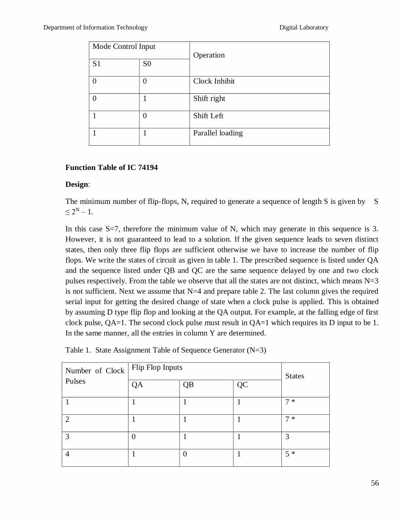
Department of Information Technology Digital Laboratory
56
Mode Control Input Operation
S1 S0
0 0 Clock Inhibit
0 1 Shift right
1 0 Shift Left
1 1 Parallel loading
Function Table of IC 74194
Design
The minimum number of flip-flops N required to generate a sequence of length S is given by S
le 2N ndash 1
In this case S=7 therefore the minimum value of N which may generate in this sequence is 3
However it is not guaranteed to lead to a solution If the given sequence leads to seven distinct
states then only three flip flops are sufficient otherwise we have to increase the number of flip
flops We write the states of circuit as given in table 1 The prescribed sequence is listed under QA
and the sequence listed under QB and QC are the same sequence delayed by one and two clock
pulses respectively From the table we observe that all the states are not distinct which means N=3
is not sufficient Next we assume that N=4 and prepare table 2 The last column gives the required
serial input for getting the desired change of state when a clock pulse is applied This is obtained
by assuming D type flip flop and looking at the QA output For example at the falling edge of first
clock pulse QA=1 The second clock pulse must result in QA=1 which requires its D input to be 1
In the same manner all the entries in column Y are determined
Table 1 State Assignment Table of Sequence Generator (N=3)
Number of Clock
Pulses
Flip Flop Inputs States
QA QB QC
1 1 1 1 7
2 1 1 1 7
3 0 1 1 3
4 1 0 1 5
Department of Information Technology Digital Laboratory
57
5 0 1 0 2
6 1 0 1 5
7 1 1 0 6
Excitation table of D Flip-Flop
Present State Qn Next State Qn+1 Flip-Flop Input D
0 0 0
0 1 1
1 0 0
1 1 1
Table 2State Assignment Table of Sequence Generator (N=4)
Number of Clock
Pulses
Flip Flop Inputs States
Y
Serial ip QA QB QC QD
1 1 1 1 0 14 1
2 1 1 1 1 15 0
3 0 1 1 1 7 1
4 1 0 1 1 11 0
5 0 1 0 1 5 1
6 1 0 1 0 10 1
7 1 1 0 1 13 1
K-Map Simplification
Department of Information Technology Digital Laboratory
58
00 01 11 10
00 X X X X
01 X 1 1 X
11 X 1 0 1
10 X X 0 1
Y= QArsquo + QBrsquo + QCrsquo = QAQBQC
LOGIC DIAGRAM
HARDWARE REQUIREMENTS
Sr no ICs Description Quantity
11 74194 4 bit bidirectional universal shift register 16ktr`
2 7410 3 input NAND Gate 1
Department of Information Technology Digital Laboratory
59
Conclusion In this way sequence generator using JK flip flips amp shift register is designed and
implemented
Enhancements Modifications ndash Sequence generator can also be implemented with shift register instead
of flip flops Use IC 7495 universal shift register IC and try to implement sequence generator
FAQs
1 What is sequential logic circuit
A sequential logic circuit consists of a memory elements in addition to
combinational circuit Its output at any instant of time depends upon
the present input as well as present state of memory element
2 What is meant by delay line
It is used to introduce time delays in digital signals
3 What is meant by following terms
a) Synchronous preset b) Asynchronous preset
c) Synchronous clear d) Asynchronous clear
a)Preset operation is synchronised with the clock
b)Preset operation is independent of the clock
c) clear is performed in synchronous with clock
d) clear is performed independent with clock
4 Is asynchronous counter faster than synchronous counter
In a synchronous counter the time required for change of any state is same and is equal to delay
time of one flip flop where as in asynchronous counter all flip flops are not clocked
simultaneously hence time required is not same
5 What is mean by lockout in counter
In a counter design for a fewer state than the maximum possible state some time it may so happen
that counter enters in unused state and goes from one unused state to another unused state and
never comes to used state
6 What is mean by state table
Department of Information Technology Digital Laboratory
60
It consists of complete information about present state and next state and outputs of a sequential
system
7 What is mean by state diagram
The information available in a state table can be represented as graphically the graphical
representation is known as state diagram
8 What is the advantage of state reduction in the design of sequential circuit
It reduces the number of flip flops
9 What is meant by excitation table
This gives information about what should be the flip flop inputs if outputs are specified before and
after the clock pulse
10 How many flip flops are required to design sequence generator using Counters
max (0rsquoS1rsquoS) in a given sequence lt= 2(N - 1)
Where N = Number of flip flops
11 How many flip flops are required to design sequence generator using shift registers
Slt= 2N - 1
Where N=Number of flip flops
S= Length of sequence
12 What is Lock out condition How it is avoided
When counter enters into one of the invalid state and after application of pulses remains in invalid
states only i e counter gets locked into invalid state amp this is called as lock out Lock out can be
avoided by providing bushing to all the invalid states in such a way that after application of one or
more clock pulses counter will fall into one of the valid state
Department of Information Technology Digital Laboratory
61
Regularity Content Viva-voce Timely
Submission Total
Dated Sign of
Subject
Teacher
2 4 2 2 10
Date of Performance Date of Completion
-------------------------------------------------------------------------------------------------------------------
Assignment No7
------------------------------------------------------------------------------------------------------------------
Title Multiplexer using Data flow modeling and structural modeling
------------------------------------------------------------------------------------------------------------------
Objective To learn data flow modeling style Its uses and different types of declarations with some
different types of circuits Structure of VHDL program is well discussed with this modeling style
-------------------------------------------------------------------------------------------------------------------
Problem Statement 41 multiplexer using data flow amp structural modeling -
----------------------------------------------------------------------------------------------------------------
Hardware Requirement - NA
----------------------------------------------------------------------------------------------------------------
Software Requirement Xilinx
------------------------------------------------------------------------------------------------------------------
Theory
Data flow style-
In this type of design the view of data as flowing from input to output through a design
An operation is defined in terms of a collection of data transformation expressed as concurrent
statement Each of the statement can be activated when any of its input signal changes its value While
these statements describe the behavior of the circuit a lot of information about its structure can be
extracted from the description as well
Data flow modeling has a set of concurrent assignment statements In the data flow level of abstraction we
describe how information is passed in the circuit The built in operators in VHDL are used in expression
such as AND OR XOR NOT etc
Department of Information Technology Digital Laboratory
62
INPUT
Two select lines S1S0
Four data lines D0 D1 D2 D3
OUTPUT
One output line Y
Functional block diagram of 41 Mux
Fig 41 Multiplexer using Data flow modeling
Function table of 41 Mux
Enable S1 S0 A B C D Y
1 X X X X X X 0
0 0 0 A X X X A
0 0 1 X B X X B
0 1 0 X X C X C
0 1 1 X X X D D
Design steps
Click on Xilinx ISE 92i
Create New project from file menu Ensure top level source is HDL
Select family of devices (usually spartan2E or 3)
Department of Information Technology Digital Laboratory
63
Ensure preferred language is VHDL
Click new source which shows you project details device details
and Synthesis and simulator tools
After finishing project create new source by right clicking in project name with VHDL
module
Complete ports name directions and bus Ensure architecture name is behavioral
After that we will get design summary and detailed reports
Close design summary
Create your code with given modeling style
Go to process window and synthesis to check if any error is there in code Check syntax and
view RTL schematic
Create new source to simulate the code
Right click on source name and create test bench waveform with proper name Ensure the
project is same
Click on combinational circuit in initial timing wizard
Select test bench wave in source window Apply inputs to wave diagram Ensure you are in
behavioral simulation
Go to process box Click on Xilinx ISE simulator and simulate the model See results
RTL Schematic
Department of Information Technology Digital Laboratory
64
Timing Diagram
FAQrsquos
1 What are the different kinds of data objects in VHDL code
Ans data object may be any value or number still some signal data objects and bit and bit_vector
types of these are available in VHDL STD_LOGIC and STD_LOGIC_VECTOR types are used
widely in programming
2 What do you mean by signal
Ans signal is a data object represents logic signals or wires in a circuit There are three places in
which signals can be declared in VHDL code in an entity declaration in the declarative section of
architecture and in declarative section of package
3 What are different signal types
Ans BIT BIT_VECTOR STD_LOGIC STD_LOGIC_VECTOR STD_ULOGIC SIGNED
UNSIGNED INTEGER ENUMERATION and BOOLEAN
4 What is an entity
Ans a circuit or sub circuit described with VHDL code is called a design entity
5 Explain structure of an entity
Ans it has two main parts the entity declaration which specifies the input and output signals for
entity and the architecture which gives circuit details
Department of Information Technology Digital Laboratory
65
6 How will you declare a package with component Explain structure
The general form of package declaration is as shown in diagram
PACKAGE package_name IS
[TYPE declarations]
[SIGNAL declarations]
[COMPONENT declarations]
END package_name
Entity
Declaration Architecture
Department of Information Technology Digital Laboratory
66
Regularity Content Viva-voce Timely
Submission Total
Dated Sign of
Subject
Teacher
2 4 2 2 10
Date of Performance Date of Completion
-------------------------------------------------------------------------------------------------------------------
Assignment No8
------------------------------------------------------------------------------------------------------------------
Title Full Adder using Behavioral and Structural modeling
------------------------------------------------------------------------------------------------------------------
Objective To learn structural modeling style Its uses and different types of declarations with some
different types of circuits Structure of VHDL program is well discussed with this modeling style
-------------------------------------------------------------------------------------------------------------------
Problem Statement Full adder using behavioral amp structural modeling
-----------------------------------------------------------------------------------------------------------------
Hardware Requirement - NA
----------------------------------------------------------------------------------------------------------------
Software Requirement Xilinx
------------------------------------------------------------------------------------------------------------------
Theory
Structural style-
A digital electronic system can be described as a module with inputs andor outputs The electrical values
on the outputs are same functions of the values of inputs The example of it is as shown The NAND gate
has 2ips AampB amp an output y Using VHDL terminology we call the NAND2 design entity amp the inputs
amp outputs are called ports 1 way of describing the function of NAND2 is to describe how it is composed
of sub modules AND amp INVERTER Each of the Sub modules is an instance of some entity amp ports of the
instances are connected using signals Structural modeling has a set of interconnected component
Structure can be used to create a very low level description of a circuit or a very high level description
Department of Information Technology Digital Laboratory
67
In a gate level description of a circuit for example components such as basic logic gates amp FFs might be
connected in some logical stricture to create the circuit This is what is often called a net list
Structure of structural modeling
Functional block diagram of Full Adder
architectureNetlistofHalf_Adderis
-- component with locals
componentMyXorport (A_XorB_Xor in BIT
Z_Xor out BIT)
end component
-- component with locals
componentMyAndport (A_AndB_And in BIT
Z_And out BIT)
end component
begin
Xor1 MyXorport map (X Y Sum)
-- instance with actuals
And1 MyAndport map (X Y Cout)
-- instance with actuals
end
Department of Information Technology Digital Laboratory
68
Function table of Full Adder
A B Cin SUM CARRY
0 0 0 0 0
0 0 1 1 0
0 1 0 1 0
0 1 1 0 1
1 0 0 1 0
1 0 1 0 1
1 1 0 0 1
1 1 1 1 1
Sum = Σm(1 2 4 7)
Carry= Σm(3 5 6 7)
Design steps
Click on Xilinx ISE 92i
Create New project from file menu Ensure top level source is HDL
Select family of devices (usually spartan2E or 3)
Ensure preferred language is VHDL
Click new source which shows you project details device details
and Synthesis and simulator tools
After finishing project create new source(full adder) by right clicking in project name with
VHDL module
Complete ports name directions and bus Ensure architecture name is behavioral
After that we will get design summary and detailed reports
Close design summary
Click new source which shows you project details device details
and Synthesis and simulator tools
After finishing project create new source(half adder) by right clicking in project name with
VHDL module
Complete ports name directions and bus Ensure architecture name is behavioral Names
should be same as previous inputs
Department of Information Technology Digital Laboratory
69
After that we will get design summary and detailed reports
Close design summary
Create your code for half adder with given modeling style
After that go to process window Click on design utilities
View HDL instantiation code of half adder
Copy component part of half adder in architecture block of full adder Copy instantiation
template twice after begin as we require two half adders to construct full adder (structural
modeling) Name them differently (eg ha1 or ha2)
Create signals as per the logic Complete code of full adder
Go to process window and synthesis to check if any error is there in code Check syntax and
view RTL schematic
Create new source to simulate the code
Right click on source name and create test bench waveform with proper name Ensure the
project is same
Click on combinational circuit in initial timing wizard
Select test bench wave in source window Apply inputs to wave diagram Ensure you are in
behavioral simulation
Go to process box Click on Xilinx ISE simulator and simulate the model See results
RTL Schematic
Timing Diagram
Department of Information Technology Digital Laboratory
70
INPUT
Three inputs A B Carry (previous)
OUTPUT
Two outputs Sum Carry
FAQrsquos
1 What do you mean by structural style
Ans in this type of code a circuit is described in hierarchical fashion by connecting together sub
circuits
2 Explain IF statement with example
Ans The general form of an IF statement is as follws
IF Sel=rsquo0rsquo THEN
Flt=x1
ELSE
Flt=x2
END IF
Department of Information Technology Digital Laboratory
71
3 Explain declaration and instantiation process in VHDL
Ans first declare a small vhdl code in formal way Eg half adder Define project name is full adder
And simply copy instantiation template in main source code Define how many times you want to
declare this template Give separate names for those
4 What is STD_LOGIC_VECTOR
Ans It is standard data object added to VHDL standard in IEEE 1164 It provides more flexibility
than the Bit type
5 Explain difference between concurrent and sequential statements
Ans Concurrent statements define interconnected processes and blocks that together describe a designrsquos
overall behavior or structure They can be grouped using block sstatement Groups of blocks can also be
partitioned into other blocks At this same level a VHDL component can be connected to define signals
within the blocks
It is a reference to an entity A process can be a single signal assignment statement or a series of
sequential statements (SS) Within a process procedures and functions can partition the sequential
statements
PRACTICE ASSIGNMENTS
1 Implement half adder using data flow modeling
2 Implement Full Adder using behavioral modeling
3 Implement 3 bit magnitude comparator using a 3 bit adder
4 Implement half sub tractor using data flow modeling
5 Write VHDL code for Full Subtractor
Department of Information Technology Digital Laboratory
72
Regularity Content Viva-voce Timely
Submission Total
Dated Sign of
Subject
Teacher
2 4 2 2 10
rsquozaDate of Performance Date of Completion
-------------------------------------------------------------------------------------------------------------------
Assignment No9
------------------------------------------------------------------------------------------------------------------
Title Simulation of 3 bit Connter using Behavioral modeling
------------------------------------------------------------------------------------------------------------------
Objective To learn behavioral modeling style Its uses and different types of declarations with some
different types of circuits Structure of VHDL program is well discussed with this modeling style
-------------------------------------------------------------------------------------------------------------------
Problem Statement 3 bit controlled up down synchronous counter with preset amp clear
-----------------------------------------------------------------------------------------------------------------
Hardware Requirement -NA
----------------------------------------------------------------------------------------------------------------
Software Requirement Xilinx
------------------------------------------------------------------------------------------------------------------
Theory
Behavioral style-
Highest level of abstraction supported in VHDL is called the behavior level of abstraction In it we have
for loop while loop If then else case ampvariable assignment The statements are enclosed in a PROCESS
block amp are executed sequentially
In it circuit is described in terms of its operation overtime
In behavioral description the concept of time may be expressed precisely with actual delays between
related events (such as the propagation delays within gates amp on wires) or it may be simply an ordering of
operation that are expressed sequentially (such as in a functional description of a FF)
Department of Information Technology Digital Laboratory
73
A behavioral design method defines a circuit in terms of text language rather than a schematic of
interconnected symbols
Behavioral design is a technology independent text based design that incorporates high level
functionality amp high level information flow
Structure of Behavioral modeling
Functional block diagram of 3 bit controlled up down synchronous counter with preset amp clear
Function table of 3 bit controlled up down synchronous counter with preset amp clear
Design steps
Click on Xilinx ISE 92i
Create New project from file menu Ensure top level source is HDL
Select family of devices (usually spartan2E or 3)
Ensure preferred language is VHDL
Click new source which shows you project details device details
and Synthesis and simulator tools
After finishing project create new source by right clicking in project name with VHDL
module
Complete ports name directions and bus Ensure architecture name is behavioral
After that we will get design summary and detailed reports
Close design summary
Create your code with given modeling style
Go to process window and synthesis to check if any error is there in code Check syntax
and view RTL schematic Create new source to simulate the code
Department of Information Technology Digital Laboratory
74
Right click on source name and create test bench waveform with proper name Ensure the
project is same
Click on combinational circuit in initial timing wizard
Select test bench wave in source window Apply inputs to wave diagram Ensure you are in
behavioral simulation
Go to process box Click on Xilinx ISE simulator and simulate the model
RTL Schematic
Timing Diagram
INPUT
Clock Preset Clear
OUTPUT
Three output lines
FAQrsquos
1 Explain the structure of behavioral modeling
2 What are the differences between behavioral and structural modeling
Ans Behavioral descriptionof a circuit is the highest level of abstraction in VHDL Here the
circuit is described in terms of it operation with respect to time All operations are in one level of
code The operations are described in a way that the designer of a sequential circuit infers a
register
Structural description on the other hand is a circuit description in terms of its components
it can either create a low level description much like a hierarchy in a block diagram Whenever
you see a component instantiated in a code that code employs structural description of the circuit
The components are connected in the form of a netlist This is for better manageability and
reusability
3 What are the differences between behavioral and data flow modeling
Department of Information Technology Digital Laboratory
75
Ans Behavioral ndash describes how the output is derived from the inputs using structured
statements
Dataflow ndash describes how the data flows from the inputs to the output most often
using NOT AND and OR operations
4 What do you mean by process statement
Ans The process statement begins with the PROCESS keyword followed by a parenthesized list
of signals called the sensitivity list It operates on selected and conditional statements
5 Explain syntax of process statement
Ans BEGIN
Process( sensitivity list)
END process
PRACTICE ASSIGNMENTS
1 Implement 3 bit asynchronous up counter using behavioral modeling
2 Implement 3 bit asynchronous down counter using behavioral modeling
3 Implement 3 bit synchronous down counter using behavioral modeling
End
Department of Information Technology Digital Laboratory
76
Pin Diagrams
7400 Quad 2-Input NAND Gate
7402 Quad 2-Input NOR Gate
7404 Not Gates
7408 Quad 2-Input AND Gates
7432 Quad 2-Input OR Gate
7486 Quad 2-Input Exclusive-OR Gate
Department of Information Technology Digital Laboratory
77
7483 4 bit Binary Adder
7490 Decade and Binary Counters
74138 38 Decoder
Department of Information Technology Digital Laboratory
78
74153 Dual 41 Multiplexer
74191 Synchronous UpDown 4 bit Binary counter with Mode Control
Department of Information Technology Digital Laboratory
79
74194 Universal Shift Register
7476 Dual Master-Slave J-K Flip-Flops
- Part B Sequence Generator using Shift Register IC 74194
-
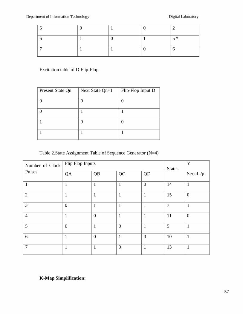
Department of Information Technology Digital Laboratory
60
It consists of complete information about present state and next state and outputs of a sequential
system
7 What is mean by state diagram
The information available in a state table can be represented as graphically the graphical
representation is known as state diagram
8 What is the advantage of state reduction in the design of sequential circuit
It reduces the number of flip flops
9 What is meant by excitation table
This gives information about what should be the flip flop inputs if outputs are specified before and
after the clock pulse
10 How many flip flops are required to design sequence generator using Counters
max (0rsquoS1rsquoS) in a given sequence lt= 2(N - 1)
Where N = Number of flip flops
11 How many flip flops are required to design sequence generator using shift registers
Slt= 2N - 1
Where N=Number of flip flops
S= Length of sequence
12 What is Lock out condition How it is avoided
When counter enters into one of the invalid state and after application of pulses remains in invalid
states only i e counter gets locked into invalid state amp this is called as lock out Lock out can be
avoided by providing bushing to all the invalid states in such a way that after application of one or
more clock pulses counter will fall into one of the valid state
Department of Information Technology Digital Laboratory
61
Regularity Content Viva-voce Timely
Submission Total
Dated Sign of
Subject
Teacher
2 4 2 2 10
Date of Performance Date of Completion
-------------------------------------------------------------------------------------------------------------------
Assignment No7
------------------------------------------------------------------------------------------------------------------
Title Multiplexer using Data flow modeling and structural modeling
------------------------------------------------------------------------------------------------------------------
Objective To learn data flow modeling style Its uses and different types of declarations with some
different types of circuits Structure of VHDL program is well discussed with this modeling style
-------------------------------------------------------------------------------------------------------------------
Problem Statement 41 multiplexer using data flow amp structural modeling -
----------------------------------------------------------------------------------------------------------------
Hardware Requirement - NA
----------------------------------------------------------------------------------------------------------------
Software Requirement Xilinx
------------------------------------------------------------------------------------------------------------------
Theory
Data flow style-
In this type of design the view of data as flowing from input to output through a design
An operation is defined in terms of a collection of data transformation expressed as concurrent
statement Each of the statement can be activated when any of its input signal changes its value While
these statements describe the behavior of the circuit a lot of information about its structure can be
extracted from the description as well
Data flow modeling has a set of concurrent assignment statements In the data flow level of abstraction we
describe how information is passed in the circuit The built in operators in VHDL are used in expression
such as AND OR XOR NOT etc
Department of Information Technology Digital Laboratory
62
INPUT
Two select lines S1S0
Four data lines D0 D1 D2 D3
OUTPUT
One output line Y
Functional block diagram of 41 Mux
Fig 41 Multiplexer using Data flow modeling
Function table of 41 Mux
Enable S1 S0 A B C D Y
1 X X X X X X 0
0 0 0 A X X X A
0 0 1 X B X X B
0 1 0 X X C X C
0 1 1 X X X D D
Design steps
Click on Xilinx ISE 92i
Create New project from file menu Ensure top level source is HDL
Select family of devices (usually spartan2E or 3)
Department of Information Technology Digital Laboratory
63
Ensure preferred language is VHDL
Click new source which shows you project details device details
and Synthesis and simulator tools
After finishing project create new source by right clicking in project name with VHDL
module
Complete ports name directions and bus Ensure architecture name is behavioral
After that we will get design summary and detailed reports
Close design summary
Create your code with given modeling style
Go to process window and synthesis to check if any error is there in code Check syntax and
view RTL schematic
Create new source to simulate the code
Right click on source name and create test bench waveform with proper name Ensure the
project is same
Click on combinational circuit in initial timing wizard
Select test bench wave in source window Apply inputs to wave diagram Ensure you are in
behavioral simulation
Go to process box Click on Xilinx ISE simulator and simulate the model See results
RTL Schematic
Department of Information Technology Digital Laboratory
64
Timing Diagram
FAQrsquos
1 What are the different kinds of data objects in VHDL code
Ans data object may be any value or number still some signal data objects and bit and bit_vector
types of these are available in VHDL STD_LOGIC and STD_LOGIC_VECTOR types are used
widely in programming
2 What do you mean by signal
Ans signal is a data object represents logic signals or wires in a circuit There are three places in
which signals can be declared in VHDL code in an entity declaration in the declarative section of
architecture and in declarative section of package
3 What are different signal types
Ans BIT BIT_VECTOR STD_LOGIC STD_LOGIC_VECTOR STD_ULOGIC SIGNED
UNSIGNED INTEGER ENUMERATION and BOOLEAN
4 What is an entity
Ans a circuit or sub circuit described with VHDL code is called a design entity
5 Explain structure of an entity
Ans it has two main parts the entity declaration which specifies the input and output signals for
entity and the architecture which gives circuit details
Department of Information Technology Digital Laboratory
65
6 How will you declare a package with component Explain structure
The general form of package declaration is as shown in diagram
PACKAGE package_name IS
[TYPE declarations]
[SIGNAL declarations]
[COMPONENT declarations]
END package_name
Entity
Declaration Architecture
Department of Information Technology Digital Laboratory
66
Regularity Content Viva-voce Timely
Submission Total
Dated Sign of
Subject
Teacher
2 4 2 2 10
Date of Performance Date of Completion
-------------------------------------------------------------------------------------------------------------------
Assignment No8
------------------------------------------------------------------------------------------------------------------
Title Full Adder using Behavioral and Structural modeling
------------------------------------------------------------------------------------------------------------------
Objective To learn structural modeling style Its uses and different types of declarations with some
different types of circuits Structure of VHDL program is well discussed with this modeling style
-------------------------------------------------------------------------------------------------------------------
Problem Statement Full adder using behavioral amp structural modeling
-----------------------------------------------------------------------------------------------------------------
Hardware Requirement - NA
----------------------------------------------------------------------------------------------------------------
Software Requirement Xilinx
------------------------------------------------------------------------------------------------------------------
Theory
Structural style-
A digital electronic system can be described as a module with inputs andor outputs The electrical values
on the outputs are same functions of the values of inputs The example of it is as shown The NAND gate
has 2ips AampB amp an output y Using VHDL terminology we call the NAND2 design entity amp the inputs
amp outputs are called ports 1 way of describing the function of NAND2 is to describe how it is composed
of sub modules AND amp INVERTER Each of the Sub modules is an instance of some entity amp ports of the
instances are connected using signals Structural modeling has a set of interconnected component
Structure can be used to create a very low level description of a circuit or a very high level description
Department of Information Technology Digital Laboratory
67
In a gate level description of a circuit for example components such as basic logic gates amp FFs might be
connected in some logical stricture to create the circuit This is what is often called a net list
Structure of structural modeling
Functional block diagram of Full Adder
architectureNetlistofHalf_Adderis
-- component with locals
componentMyXorport (A_XorB_Xor in BIT
Z_Xor out BIT)
end component
-- component with locals
componentMyAndport (A_AndB_And in BIT
Z_And out BIT)
end component
begin
Xor1 MyXorport map (X Y Sum)
-- instance with actuals
And1 MyAndport map (X Y Cout)
-- instance with actuals
end
Department of Information Technology Digital Laboratory
68
Function table of Full Adder
A B Cin SUM CARRY
0 0 0 0 0
0 0 1 1 0
0 1 0 1 0
0 1 1 0 1
1 0 0 1 0
1 0 1 0 1
1 1 0 0 1
1 1 1 1 1
Sum = Σm(1 2 4 7)
Carry= Σm(3 5 6 7)
Design steps
Click on Xilinx ISE 92i
Create New project from file menu Ensure top level source is HDL
Select family of devices (usually spartan2E or 3)
Ensure preferred language is VHDL
Click new source which shows you project details device details
and Synthesis and simulator tools
After finishing project create new source(full adder) by right clicking in project name with
VHDL module
Complete ports name directions and bus Ensure architecture name is behavioral
After that we will get design summary and detailed reports
Close design summary
Click new source which shows you project details device details
and Synthesis and simulator tools
After finishing project create new source(half adder) by right clicking in project name with
VHDL module
Complete ports name directions and bus Ensure architecture name is behavioral Names
should be same as previous inputs
Department of Information Technology Digital Laboratory
69
After that we will get design summary and detailed reports
Close design summary
Create your code for half adder with given modeling style
After that go to process window Click on design utilities
View HDL instantiation code of half adder
Copy component part of half adder in architecture block of full adder Copy instantiation
template twice after begin as we require two half adders to construct full adder (structural
modeling) Name them differently (eg ha1 or ha2)
Create signals as per the logic Complete code of full adder
Go to process window and synthesis to check if any error is there in code Check syntax and
view RTL schematic
Create new source to simulate the code
Right click on source name and create test bench waveform with proper name Ensure the
project is same
Click on combinational circuit in initial timing wizard
Select test bench wave in source window Apply inputs to wave diagram Ensure you are in
behavioral simulation
Go to process box Click on Xilinx ISE simulator and simulate the model See results
RTL Schematic
Timing Diagram
Department of Information Technology Digital Laboratory
70
INPUT
Three inputs A B Carry (previous)
OUTPUT
Two outputs Sum Carry
FAQrsquos
1 What do you mean by structural style
Ans in this type of code a circuit is described in hierarchical fashion by connecting together sub
circuits
2 Explain IF statement with example
Ans The general form of an IF statement is as follws
IF Sel=rsquo0rsquo THEN
Flt=x1
ELSE
Flt=x2
END IF
Department of Information Technology Digital Laboratory
71
3 Explain declaration and instantiation process in VHDL
Ans first declare a small vhdl code in formal way Eg half adder Define project name is full adder
And simply copy instantiation template in main source code Define how many times you want to
declare this template Give separate names for those
4 What is STD_LOGIC_VECTOR
Ans It is standard data object added to VHDL standard in IEEE 1164 It provides more flexibility
than the Bit type
5 Explain difference between concurrent and sequential statements
Ans Concurrent statements define interconnected processes and blocks that together describe a designrsquos
overall behavior or structure They can be grouped using block sstatement Groups of blocks can also be
partitioned into other blocks At this same level a VHDL component can be connected to define signals
within the blocks
It is a reference to an entity A process can be a single signal assignment statement or a series of
sequential statements (SS) Within a process procedures and functions can partition the sequential
statements
PRACTICE ASSIGNMENTS
1 Implement half adder using data flow modeling
2 Implement Full Adder using behavioral modeling
3 Implement 3 bit magnitude comparator using a 3 bit adder
4 Implement half sub tractor using data flow modeling
5 Write VHDL code for Full Subtractor
Department of Information Technology Digital Laboratory
72
Regularity Content Viva-voce Timely
Submission Total
Dated Sign of
Subject
Teacher
2 4 2 2 10
rsquozaDate of Performance Date of Completion
-------------------------------------------------------------------------------------------------------------------
Assignment No9
------------------------------------------------------------------------------------------------------------------
Title Simulation of 3 bit Connter using Behavioral modeling
------------------------------------------------------------------------------------------------------------------
Objective To learn behavioral modeling style Its uses and different types of declarations with some
different types of circuits Structure of VHDL program is well discussed with this modeling style
-------------------------------------------------------------------------------------------------------------------
Problem Statement 3 bit controlled up down synchronous counter with preset amp clear
-----------------------------------------------------------------------------------------------------------------
Hardware Requirement -NA
----------------------------------------------------------------------------------------------------------------
Software Requirement Xilinx
------------------------------------------------------------------------------------------------------------------
Theory
Behavioral style-
Highest level of abstraction supported in VHDL is called the behavior level of abstraction In it we have
for loop while loop If then else case ampvariable assignment The statements are enclosed in a PROCESS
block amp are executed sequentially
In it circuit is described in terms of its operation overtime
In behavioral description the concept of time may be expressed precisely with actual delays between
related events (such as the propagation delays within gates amp on wires) or it may be simply an ordering of
operation that are expressed sequentially (such as in a functional description of a FF)
Department of Information Technology Digital Laboratory
73
A behavioral design method defines a circuit in terms of text language rather than a schematic of
interconnected symbols
Behavioral design is a technology independent text based design that incorporates high level
functionality amp high level information flow
Structure of Behavioral modeling
Functional block diagram of 3 bit controlled up down synchronous counter with preset amp clear
Function table of 3 bit controlled up down synchronous counter with preset amp clear
Design steps
Click on Xilinx ISE 92i
Create New project from file menu Ensure top level source is HDL
Select family of devices (usually spartan2E or 3)
Ensure preferred language is VHDL
Click new source which shows you project details device details
and Synthesis and simulator tools
After finishing project create new source by right clicking in project name with VHDL
module
Complete ports name directions and bus Ensure architecture name is behavioral
After that we will get design summary and detailed reports
Close design summary
Create your code with given modeling style
Go to process window and synthesis to check if any error is there in code Check syntax
and view RTL schematic Create new source to simulate the code
Department of Information Technology Digital Laboratory
74
Right click on source name and create test bench waveform with proper name Ensure the
project is same
Click on combinational circuit in initial timing wizard
Select test bench wave in source window Apply inputs to wave diagram Ensure you are in
behavioral simulation
Go to process box Click on Xilinx ISE simulator and simulate the model
RTL Schematic
Timing Diagram
INPUT
Clock Preset Clear
OUTPUT
Three output lines
FAQrsquos
1 Explain the structure of behavioral modeling
2 What are the differences between behavioral and structural modeling
Ans Behavioral descriptionof a circuit is the highest level of abstraction in VHDL Here the
circuit is described in terms of it operation with respect to time All operations are in one level of
code The operations are described in a way that the designer of a sequential circuit infers a
register
Structural description on the other hand is a circuit description in terms of its components
it can either create a low level description much like a hierarchy in a block diagram Whenever
you see a component instantiated in a code that code employs structural description of the circuit
The components are connected in the form of a netlist This is for better manageability and
reusability
3 What are the differences between behavioral and data flow modeling
Department of Information Technology Digital Laboratory
75
Ans Behavioral ndash describes how the output is derived from the inputs using structured
statements
Dataflow ndash describes how the data flows from the inputs to the output most often
using NOT AND and OR operations
4 What do you mean by process statement
Ans The process statement begins with the PROCESS keyword followed by a parenthesized list
of signals called the sensitivity list It operates on selected and conditional statements
5 Explain syntax of process statement
Ans BEGIN
Process( sensitivity list)
END process
PRACTICE ASSIGNMENTS
1 Implement 3 bit asynchronous up counter using behavioral modeling
2 Implement 3 bit asynchronous down counter using behavioral modeling
3 Implement 3 bit synchronous down counter using behavioral modeling
End
Department of Information Technology Digital Laboratory
76
Pin Diagrams
7400 Quad 2-Input NAND Gate
7402 Quad 2-Input NOR Gate
7404 Not Gates
7408 Quad 2-Input AND Gates
7432 Quad 2-Input OR Gate
7486 Quad 2-Input Exclusive-OR Gate
Department of Information Technology Digital Laboratory
77
7483 4 bit Binary Adder
7490 Decade and Binary Counters
74138 38 Decoder
Department of Information Technology Digital Laboratory
78
74153 Dual 41 Multiplexer
74191 Synchronous UpDown 4 bit Binary counter with Mode Control
Department of Information Technology Digital Laboratory
79
74194 Universal Shift Register
7476 Dual Master-Slave J-K Flip-Flops
- Part B Sequence Generator using Shift Register IC 74194
-
Department of Information Technology Digital Laboratory
61
Regularity Content Viva-voce Timely
Submission Total
Dated Sign of
Subject
Teacher
2 4 2 2 10
Date of Performance Date of Completion
-------------------------------------------------------------------------------------------------------------------
Assignment No7
------------------------------------------------------------------------------------------------------------------
Title Multiplexer using Data flow modeling and structural modeling
------------------------------------------------------------------------------------------------------------------
Objective To learn data flow modeling style Its uses and different types of declarations with some
different types of circuits Structure of VHDL program is well discussed with this modeling style
-------------------------------------------------------------------------------------------------------------------
Problem Statement 41 multiplexer using data flow amp structural modeling -
----------------------------------------------------------------------------------------------------------------
Hardware Requirement - NA
----------------------------------------------------------------------------------------------------------------
Software Requirement Xilinx
------------------------------------------------------------------------------------------------------------------
Theory
Data flow style-
In this type of design the view of data as flowing from input to output through a design
An operation is defined in terms of a collection of data transformation expressed as concurrent
statement Each of the statement can be activated when any of its input signal changes its value While
these statements describe the behavior of the circuit a lot of information about its structure can be
extracted from the description as well
Data flow modeling has a set of concurrent assignment statements In the data flow level of abstraction we
describe how information is passed in the circuit The built in operators in VHDL are used in expression
such as AND OR XOR NOT etc
Department of Information Technology Digital Laboratory
62
INPUT
Two select lines S1S0
Four data lines D0 D1 D2 D3
OUTPUT
One output line Y
Functional block diagram of 41 Mux
Fig 41 Multiplexer using Data flow modeling
Function table of 41 Mux
Enable S1 S0 A B C D Y
1 X X X X X X 0
0 0 0 A X X X A
0 0 1 X B X X B
0 1 0 X X C X C
0 1 1 X X X D D
Design steps
Click on Xilinx ISE 92i
Create New project from file menu Ensure top level source is HDL
Select family of devices (usually spartan2E or 3)
Department of Information Technology Digital Laboratory
63
Ensure preferred language is VHDL
Click new source which shows you project details device details
and Synthesis and simulator tools
After finishing project create new source by right clicking in project name with VHDL
module
Complete ports name directions and bus Ensure architecture name is behavioral
After that we will get design summary and detailed reports
Close design summary
Create your code with given modeling style
Go to process window and synthesis to check if any error is there in code Check syntax and
view RTL schematic
Create new source to simulate the code
Right click on source name and create test bench waveform with proper name Ensure the
project is same
Click on combinational circuit in initial timing wizard
Select test bench wave in source window Apply inputs to wave diagram Ensure you are in
behavioral simulation
Go to process box Click on Xilinx ISE simulator and simulate the model See results
RTL Schematic
Department of Information Technology Digital Laboratory
64
Timing Diagram
FAQrsquos
1 What are the different kinds of data objects in VHDL code
Ans data object may be any value or number still some signal data objects and bit and bit_vector
types of these are available in VHDL STD_LOGIC and STD_LOGIC_VECTOR types are used
widely in programming
2 What do you mean by signal
Ans signal is a data object represents logic signals or wires in a circuit There are three places in
which signals can be declared in VHDL code in an entity declaration in the declarative section of
architecture and in declarative section of package
3 What are different signal types
Ans BIT BIT_VECTOR STD_LOGIC STD_LOGIC_VECTOR STD_ULOGIC SIGNED
UNSIGNED INTEGER ENUMERATION and BOOLEAN
4 What is an entity
Ans a circuit or sub circuit described with VHDL code is called a design entity
5 Explain structure of an entity
Ans it has two main parts the entity declaration which specifies the input and output signals for
entity and the architecture which gives circuit details
Department of Information Technology Digital Laboratory
65
6 How will you declare a package with component Explain structure
The general form of package declaration is as shown in diagram
PACKAGE package_name IS
[TYPE declarations]
[SIGNAL declarations]
[COMPONENT declarations]
END package_name
Entity
Declaration Architecture
Department of Information Technology Digital Laboratory
66
Regularity Content Viva-voce Timely
Submission Total
Dated Sign of
Subject
Teacher
2 4 2 2 10
Date of Performance Date of Completion
-------------------------------------------------------------------------------------------------------------------
Assignment No8
------------------------------------------------------------------------------------------------------------------
Title Full Adder using Behavioral and Structural modeling
------------------------------------------------------------------------------------------------------------------
Objective To learn structural modeling style Its uses and different types of declarations with some
different types of circuits Structure of VHDL program is well discussed with this modeling style
-------------------------------------------------------------------------------------------------------------------
Problem Statement Full adder using behavioral amp structural modeling
-----------------------------------------------------------------------------------------------------------------
Hardware Requirement - NA
----------------------------------------------------------------------------------------------------------------
Software Requirement Xilinx
------------------------------------------------------------------------------------------------------------------
Theory
Structural style-
A digital electronic system can be described as a module with inputs andor outputs The electrical values
on the outputs are same functions of the values of inputs The example of it is as shown The NAND gate
has 2ips AampB amp an output y Using VHDL terminology we call the NAND2 design entity amp the inputs
amp outputs are called ports 1 way of describing the function of NAND2 is to describe how it is composed
of sub modules AND amp INVERTER Each of the Sub modules is an instance of some entity amp ports of the
instances are connected using signals Structural modeling has a set of interconnected component
Structure can be used to create a very low level description of a circuit or a very high level description
Department of Information Technology Digital Laboratory
67
In a gate level description of a circuit for example components such as basic logic gates amp FFs might be
connected in some logical stricture to create the circuit This is what is often called a net list
Structure of structural modeling
Functional block diagram of Full Adder
architectureNetlistofHalf_Adderis
-- component with locals
componentMyXorport (A_XorB_Xor in BIT
Z_Xor out BIT)
end component
-- component with locals
componentMyAndport (A_AndB_And in BIT
Z_And out BIT)
end component
begin
Xor1 MyXorport map (X Y Sum)
-- instance with actuals
And1 MyAndport map (X Y Cout)
-- instance with actuals
end
Department of Information Technology Digital Laboratory
68
Function table of Full Adder
A B Cin SUM CARRY
0 0 0 0 0
0 0 1 1 0
0 1 0 1 0
0 1 1 0 1
1 0 0 1 0
1 0 1 0 1
1 1 0 0 1
1 1 1 1 1
Sum = Σm(1 2 4 7)
Carry= Σm(3 5 6 7)
Design steps
Click on Xilinx ISE 92i
Create New project from file menu Ensure top level source is HDL
Select family of devices (usually spartan2E or 3)
Ensure preferred language is VHDL
Click new source which shows you project details device details
and Synthesis and simulator tools
After finishing project create new source(full adder) by right clicking in project name with
VHDL module
Complete ports name directions and bus Ensure architecture name is behavioral
After that we will get design summary and detailed reports
Close design summary
Click new source which shows you project details device details
and Synthesis and simulator tools
After finishing project create new source(half adder) by right clicking in project name with
VHDL module
Complete ports name directions and bus Ensure architecture name is behavioral Names
should be same as previous inputs
Department of Information Technology Digital Laboratory
69
After that we will get design summary and detailed reports
Close design summary
Create your code for half adder with given modeling style
After that go to process window Click on design utilities
View HDL instantiation code of half adder
Copy component part of half adder in architecture block of full adder Copy instantiation
template twice after begin as we require two half adders to construct full adder (structural
modeling) Name them differently (eg ha1 or ha2)
Create signals as per the logic Complete code of full adder
Go to process window and synthesis to check if any error is there in code Check syntax and
view RTL schematic
Create new source to simulate the code
Right click on source name and create test bench waveform with proper name Ensure the
project is same
Click on combinational circuit in initial timing wizard
Select test bench wave in source window Apply inputs to wave diagram Ensure you are in
behavioral simulation
Go to process box Click on Xilinx ISE simulator and simulate the model See results
RTL Schematic
Timing Diagram
Department of Information Technology Digital Laboratory
70
INPUT
Three inputs A B Carry (previous)
OUTPUT
Two outputs Sum Carry
FAQrsquos
1 What do you mean by structural style
Ans in this type of code a circuit is described in hierarchical fashion by connecting together sub
circuits
2 Explain IF statement with example
Ans The general form of an IF statement is as follws
IF Sel=rsquo0rsquo THEN
Flt=x1
ELSE
Flt=x2
END IF
Department of Information Technology Digital Laboratory
71
3 Explain declaration and instantiation process in VHDL
Ans first declare a small vhdl code in formal way Eg half adder Define project name is full adder
And simply copy instantiation template in main source code Define how many times you want to
declare this template Give separate names for those
4 What is STD_LOGIC_VECTOR
Ans It is standard data object added to VHDL standard in IEEE 1164 It provides more flexibility
than the Bit type
5 Explain difference between concurrent and sequential statements
Ans Concurrent statements define interconnected processes and blocks that together describe a designrsquos
overall behavior or structure They can be grouped using block sstatement Groups of blocks can also be
partitioned into other blocks At this same level a VHDL component can be connected to define signals
within the blocks
It is a reference to an entity A process can be a single signal assignment statement or a series of
sequential statements (SS) Within a process procedures and functions can partition the sequential
statements
PRACTICE ASSIGNMENTS
1 Implement half adder using data flow modeling
2 Implement Full Adder using behavioral modeling
3 Implement 3 bit magnitude comparator using a 3 bit adder
4 Implement half sub tractor using data flow modeling
5 Write VHDL code for Full Subtractor
Department of Information Technology Digital Laboratory
72
Regularity Content Viva-voce Timely
Submission Total
Dated Sign of
Subject
Teacher
2 4 2 2 10
rsquozaDate of Performance Date of Completion
-------------------------------------------------------------------------------------------------------------------
Assignment No9
------------------------------------------------------------------------------------------------------------------
Title Simulation of 3 bit Connter using Behavioral modeling
------------------------------------------------------------------------------------------------------------------
Objective To learn behavioral modeling style Its uses and different types of declarations with some
different types of circuits Structure of VHDL program is well discussed with this modeling style
-------------------------------------------------------------------------------------------------------------------
Problem Statement 3 bit controlled up down synchronous counter with preset amp clear
-----------------------------------------------------------------------------------------------------------------
Hardware Requirement -NA
----------------------------------------------------------------------------------------------------------------
Software Requirement Xilinx
------------------------------------------------------------------------------------------------------------------
Theory
Behavioral style-
Highest level of abstraction supported in VHDL is called the behavior level of abstraction In it we have
for loop while loop If then else case ampvariable assignment The statements are enclosed in a PROCESS
block amp are executed sequentially
In it circuit is described in terms of its operation overtime
In behavioral description the concept of time may be expressed precisely with actual delays between
related events (such as the propagation delays within gates amp on wires) or it may be simply an ordering of
operation that are expressed sequentially (such as in a functional description of a FF)
Department of Information Technology Digital Laboratory
73
A behavioral design method defines a circuit in terms of text language rather than a schematic of
interconnected symbols
Behavioral design is a technology independent text based design that incorporates high level
functionality amp high level information flow
Structure of Behavioral modeling
Functional block diagram of 3 bit controlled up down synchronous counter with preset amp clear
Function table of 3 bit controlled up down synchronous counter with preset amp clear
Design steps
Click on Xilinx ISE 92i
Create New project from file menu Ensure top level source is HDL
Select family of devices (usually spartan2E or 3)
Ensure preferred language is VHDL
Click new source which shows you project details device details
and Synthesis and simulator tools
After finishing project create new source by right clicking in project name with VHDL
module
Complete ports name directions and bus Ensure architecture name is behavioral
After that we will get design summary and detailed reports
Close design summary
Create your code with given modeling style
Go to process window and synthesis to check if any error is there in code Check syntax
and view RTL schematic Create new source to simulate the code
Department of Information Technology Digital Laboratory
74
Right click on source name and create test bench waveform with proper name Ensure the
project is same
Click on combinational circuit in initial timing wizard
Select test bench wave in source window Apply inputs to wave diagram Ensure you are in
behavioral simulation
Go to process box Click on Xilinx ISE simulator and simulate the model
RTL Schematic
Timing Diagram
INPUT
Clock Preset Clear
OUTPUT
Three output lines
FAQrsquos
1 Explain the structure of behavioral modeling
2 What are the differences between behavioral and structural modeling
Ans Behavioral descriptionof a circuit is the highest level of abstraction in VHDL Here the
circuit is described in terms of it operation with respect to time All operations are in one level of
code The operations are described in a way that the designer of a sequential circuit infers a
register
Structural description on the other hand is a circuit description in terms of its components
it can either create a low level description much like a hierarchy in a block diagram Whenever
you see a component instantiated in a code that code employs structural description of the circuit
The components are connected in the form of a netlist This is for better manageability and
reusability
3 What are the differences between behavioral and data flow modeling
Department of Information Technology Digital Laboratory
75
Ans Behavioral ndash describes how the output is derived from the inputs using structured
statements
Dataflow ndash describes how the data flows from the inputs to the output most often
using NOT AND and OR operations
4 What do you mean by process statement
Ans The process statement begins with the PROCESS keyword followed by a parenthesized list
of signals called the sensitivity list It operates on selected and conditional statements
5 Explain syntax of process statement
Ans BEGIN
Process( sensitivity list)
END process
PRACTICE ASSIGNMENTS
1 Implement 3 bit asynchronous up counter using behavioral modeling
2 Implement 3 bit asynchronous down counter using behavioral modeling
3 Implement 3 bit synchronous down counter using behavioral modeling
End
Department of Information Technology Digital Laboratory
76
Pin Diagrams
7400 Quad 2-Input NAND Gate
7402 Quad 2-Input NOR Gate
7404 Not Gates
7408 Quad 2-Input AND Gates
7432 Quad 2-Input OR Gate
7486 Quad 2-Input Exclusive-OR Gate
Department of Information Technology Digital Laboratory
77
7483 4 bit Binary Adder
7490 Decade and Binary Counters
74138 38 Decoder
Department of Information Technology Digital Laboratory
78
74153 Dual 41 Multiplexer
74191 Synchronous UpDown 4 bit Binary counter with Mode Control
Department of Information Technology Digital Laboratory
79
74194 Universal Shift Register
7476 Dual Master-Slave J-K Flip-Flops
- Part B Sequence Generator using Shift Register IC 74194
-
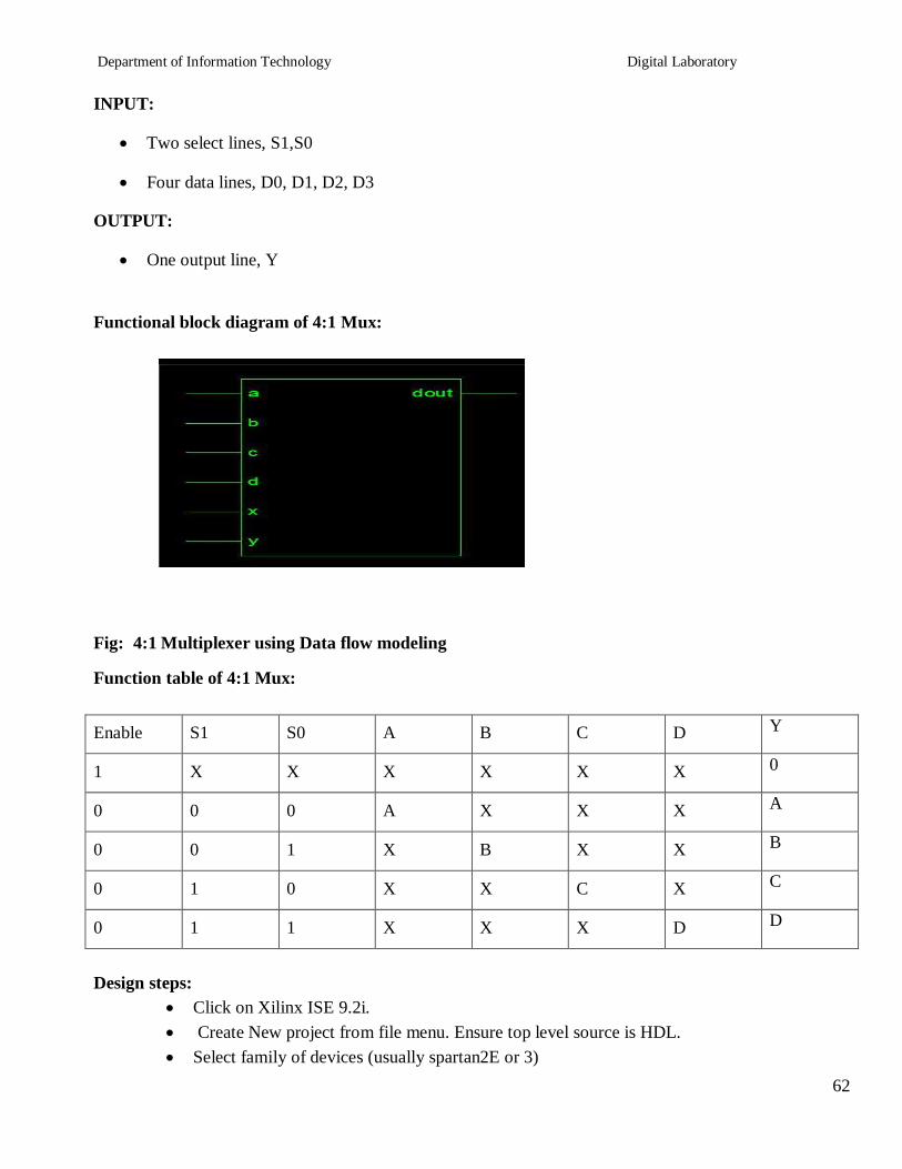
Department of Information Technology Digital Laboratory
62
INPUT
Two select lines S1S0
Four data lines D0 D1 D2 D3
OUTPUT
One output line Y
Functional block diagram of 41 Mux
Fig 41 Multiplexer using Data flow modeling
Function table of 41 Mux
Enable S1 S0 A B C D Y
1 X X X X X X 0
0 0 0 A X X X A
0 0 1 X B X X B
0 1 0 X X C X C
0 1 1 X X X D D
Design steps
Click on Xilinx ISE 92i
Create New project from file menu Ensure top level source is HDL
Select family of devices (usually spartan2E or 3)
Department of Information Technology Digital Laboratory
63
Ensure preferred language is VHDL
Click new source which shows you project details device details
and Synthesis and simulator tools
After finishing project create new source by right clicking in project name with VHDL
module
Complete ports name directions and bus Ensure architecture name is behavioral
After that we will get design summary and detailed reports
Close design summary
Create your code with given modeling style
Go to process window and synthesis to check if any error is there in code Check syntax and
view RTL schematic
Create new source to simulate the code
Right click on source name and create test bench waveform with proper name Ensure the
project is same
Click on combinational circuit in initial timing wizard
Select test bench wave in source window Apply inputs to wave diagram Ensure you are in
behavioral simulation
Go to process box Click on Xilinx ISE simulator and simulate the model See results
RTL Schematic
Department of Information Technology Digital Laboratory
64
Timing Diagram
FAQrsquos
1 What are the different kinds of data objects in VHDL code
Ans data object may be any value or number still some signal data objects and bit and bit_vector
types of these are available in VHDL STD_LOGIC and STD_LOGIC_VECTOR types are used
widely in programming
2 What do you mean by signal
Ans signal is a data object represents logic signals or wires in a circuit There are three places in
which signals can be declared in VHDL code in an entity declaration in the declarative section of
architecture and in declarative section of package
3 What are different signal types
Ans BIT BIT_VECTOR STD_LOGIC STD_LOGIC_VECTOR STD_ULOGIC SIGNED
UNSIGNED INTEGER ENUMERATION and BOOLEAN
4 What is an entity
Ans a circuit or sub circuit described with VHDL code is called a design entity
5 Explain structure of an entity
Ans it has two main parts the entity declaration which specifies the input and output signals for
entity and the architecture which gives circuit details
Department of Information Technology Digital Laboratory
65
6 How will you declare a package with component Explain structure
The general form of package declaration is as shown in diagram
PACKAGE package_name IS
[TYPE declarations]
[SIGNAL declarations]
[COMPONENT declarations]
END package_name
Entity
Declaration Architecture
Department of Information Technology Digital Laboratory
66
Regularity Content Viva-voce Timely
Submission Total
Dated Sign of
Subject
Teacher
2 4 2 2 10
Date of Performance Date of Completion
-------------------------------------------------------------------------------------------------------------------
Assignment No8
------------------------------------------------------------------------------------------------------------------
Title Full Adder using Behavioral and Structural modeling
------------------------------------------------------------------------------------------------------------------
Objective To learn structural modeling style Its uses and different types of declarations with some
different types of circuits Structure of VHDL program is well discussed with this modeling style
-------------------------------------------------------------------------------------------------------------------
Problem Statement Full adder using behavioral amp structural modeling
-----------------------------------------------------------------------------------------------------------------
Hardware Requirement - NA
----------------------------------------------------------------------------------------------------------------
Software Requirement Xilinx
------------------------------------------------------------------------------------------------------------------
Theory
Structural style-
A digital electronic system can be described as a module with inputs andor outputs The electrical values
on the outputs are same functions of the values of inputs The example of it is as shown The NAND gate
has 2ips AampB amp an output y Using VHDL terminology we call the NAND2 design entity amp the inputs
amp outputs are called ports 1 way of describing the function of NAND2 is to describe how it is composed
of sub modules AND amp INVERTER Each of the Sub modules is an instance of some entity amp ports of the
instances are connected using signals Structural modeling has a set of interconnected component
Structure can be used to create a very low level description of a circuit or a very high level description
Department of Information Technology Digital Laboratory
67
In a gate level description of a circuit for example components such as basic logic gates amp FFs might be
connected in some logical stricture to create the circuit This is what is often called a net list
Structure of structural modeling
Functional block diagram of Full Adder
architectureNetlistofHalf_Adderis
-- component with locals
componentMyXorport (A_XorB_Xor in BIT
Z_Xor out BIT)
end component
-- component with locals
componentMyAndport (A_AndB_And in BIT
Z_And out BIT)
end component
begin
Xor1 MyXorport map (X Y Sum)
-- instance with actuals
And1 MyAndport map (X Y Cout)
-- instance with actuals
end
Department of Information Technology Digital Laboratory
68
Function table of Full Adder
A B Cin SUM CARRY
0 0 0 0 0
0 0 1 1 0
0 1 0 1 0
0 1 1 0 1
1 0 0 1 0
1 0 1 0 1
1 1 0 0 1
1 1 1 1 1
Sum = Σm(1 2 4 7)
Carry= Σm(3 5 6 7)
Design steps
Click on Xilinx ISE 92i
Create New project from file menu Ensure top level source is HDL
Select family of devices (usually spartan2E or 3)
Ensure preferred language is VHDL
Click new source which shows you project details device details
and Synthesis and simulator tools
After finishing project create new source(full adder) by right clicking in project name with
VHDL module
Complete ports name directions and bus Ensure architecture name is behavioral
After that we will get design summary and detailed reports
Close design summary
Click new source which shows you project details device details
and Synthesis and simulator tools
After finishing project create new source(half adder) by right clicking in project name with
VHDL module
Complete ports name directions and bus Ensure architecture name is behavioral Names
should be same as previous inputs
Department of Information Technology Digital Laboratory
69
After that we will get design summary and detailed reports
Close design summary
Create your code for half adder with given modeling style
After that go to process window Click on design utilities
View HDL instantiation code of half adder
Copy component part of half adder in architecture block of full adder Copy instantiation
template twice after begin as we require two half adders to construct full adder (structural
modeling) Name them differently (eg ha1 or ha2)
Create signals as per the logic Complete code of full adder
Go to process window and synthesis to check if any error is there in code Check syntax and
view RTL schematic
Create new source to simulate the code
Right click on source name and create test bench waveform with proper name Ensure the
project is same
Click on combinational circuit in initial timing wizard
Select test bench wave in source window Apply inputs to wave diagram Ensure you are in
behavioral simulation
Go to process box Click on Xilinx ISE simulator and simulate the model See results
RTL Schematic
Timing Diagram
Department of Information Technology Digital Laboratory
70
INPUT
Three inputs A B Carry (previous)
OUTPUT
Two outputs Sum Carry
FAQrsquos
1 What do you mean by structural style
Ans in this type of code a circuit is described in hierarchical fashion by connecting together sub
circuits
2 Explain IF statement with example
Ans The general form of an IF statement is as follws
IF Sel=rsquo0rsquo THEN
Flt=x1
ELSE
Flt=x2
END IF
Department of Information Technology Digital Laboratory
71
3 Explain declaration and instantiation process in VHDL
Ans first declare a small vhdl code in formal way Eg half adder Define project name is full adder
And simply copy instantiation template in main source code Define how many times you want to
declare this template Give separate names for those
4 What is STD_LOGIC_VECTOR
Ans It is standard data object added to VHDL standard in IEEE 1164 It provides more flexibility
than the Bit type
5 Explain difference between concurrent and sequential statements
Ans Concurrent statements define interconnected processes and blocks that together describe a designrsquos
overall behavior or structure They can be grouped using block sstatement Groups of blocks can also be
partitioned into other blocks At this same level a VHDL component can be connected to define signals
within the blocks
It is a reference to an entity A process can be a single signal assignment statement or a series of
sequential statements (SS) Within a process procedures and functions can partition the sequential
statements
PRACTICE ASSIGNMENTS
1 Implement half adder using data flow modeling
2 Implement Full Adder using behavioral modeling
3 Implement 3 bit magnitude comparator using a 3 bit adder
4 Implement half sub tractor using data flow modeling
5 Write VHDL code for Full Subtractor
Department of Information Technology Digital Laboratory
72
Regularity Content Viva-voce Timely
Submission Total
Dated Sign of
Subject
Teacher
2 4 2 2 10
rsquozaDate of Performance Date of Completion
-------------------------------------------------------------------------------------------------------------------
Assignment No9
------------------------------------------------------------------------------------------------------------------
Title Simulation of 3 bit Connter using Behavioral modeling
------------------------------------------------------------------------------------------------------------------
Objective To learn behavioral modeling style Its uses and different types of declarations with some
different types of circuits Structure of VHDL program is well discussed with this modeling style
-------------------------------------------------------------------------------------------------------------------
Problem Statement 3 bit controlled up down synchronous counter with preset amp clear
-----------------------------------------------------------------------------------------------------------------
Hardware Requirement -NA
----------------------------------------------------------------------------------------------------------------
Software Requirement Xilinx
------------------------------------------------------------------------------------------------------------------
Theory
Behavioral style-
Highest level of abstraction supported in VHDL is called the behavior level of abstraction In it we have
for loop while loop If then else case ampvariable assignment The statements are enclosed in a PROCESS
block amp are executed sequentially
In it circuit is described in terms of its operation overtime
In behavioral description the concept of time may be expressed precisely with actual delays between
related events (such as the propagation delays within gates amp on wires) or it may be simply an ordering of
operation that are expressed sequentially (such as in a functional description of a FF)
Department of Information Technology Digital Laboratory
73
A behavioral design method defines a circuit in terms of text language rather than a schematic of
interconnected symbols
Behavioral design is a technology independent text based design that incorporates high level
functionality amp high level information flow
Structure of Behavioral modeling
Functional block diagram of 3 bit controlled up down synchronous counter with preset amp clear
Function table of 3 bit controlled up down synchronous counter with preset amp clear
Design steps
Click on Xilinx ISE 92i
Create New project from file menu Ensure top level source is HDL
Select family of devices (usually spartan2E or 3)
Ensure preferred language is VHDL
Click new source which shows you project details device details
and Synthesis and simulator tools
After finishing project create new source by right clicking in project name with VHDL
module
Complete ports name directions and bus Ensure architecture name is behavioral
After that we will get design summary and detailed reports
Close design summary
Create your code with given modeling style
Go to process window and synthesis to check if any error is there in code Check syntax
and view RTL schematic Create new source to simulate the code
Department of Information Technology Digital Laboratory
74
Right click on source name and create test bench waveform with proper name Ensure the
project is same
Click on combinational circuit in initial timing wizard
Select test bench wave in source window Apply inputs to wave diagram Ensure you are in
behavioral simulation
Go to process box Click on Xilinx ISE simulator and simulate the model
RTL Schematic
Timing Diagram
INPUT
Clock Preset Clear
OUTPUT
Three output lines
FAQrsquos
1 Explain the structure of behavioral modeling
2 What are the differences between behavioral and structural modeling
Ans Behavioral descriptionof a circuit is the highest level of abstraction in VHDL Here the
circuit is described in terms of it operation with respect to time All operations are in one level of
code The operations are described in a way that the designer of a sequential circuit infers a
register
Structural description on the other hand is a circuit description in terms of its components
it can either create a low level description much like a hierarchy in a block diagram Whenever
you see a component instantiated in a code that code employs structural description of the circuit
The components are connected in the form of a netlist This is for better manageability and
reusability
3 What are the differences between behavioral and data flow modeling
Department of Information Technology Digital Laboratory
75
Ans Behavioral ndash describes how the output is derived from the inputs using structured
statements
Dataflow ndash describes how the data flows from the inputs to the output most often
using NOT AND and OR operations
4 What do you mean by process statement
Ans The process statement begins with the PROCESS keyword followed by a parenthesized list
of signals called the sensitivity list It operates on selected and conditional statements
5 Explain syntax of process statement
Ans BEGIN
Process( sensitivity list)
END process
PRACTICE ASSIGNMENTS
1 Implement 3 bit asynchronous up counter using behavioral modeling
2 Implement 3 bit asynchronous down counter using behavioral modeling
3 Implement 3 bit synchronous down counter using behavioral modeling
End
Department of Information Technology Digital Laboratory
76
Pin Diagrams
7400 Quad 2-Input NAND Gate
7402 Quad 2-Input NOR Gate
7404 Not Gates
7408 Quad 2-Input AND Gates
7432 Quad 2-Input OR Gate
7486 Quad 2-Input Exclusive-OR Gate
Department of Information Technology Digital Laboratory
77
7483 4 bit Binary Adder
7490 Decade and Binary Counters
74138 38 Decoder
Department of Information Technology Digital Laboratory
78
74153 Dual 41 Multiplexer
74191 Synchronous UpDown 4 bit Binary counter with Mode Control
Department of Information Technology Digital Laboratory
79
74194 Universal Shift Register
7476 Dual Master-Slave J-K Flip-Flops
- Part B Sequence Generator using Shift Register IC 74194
-
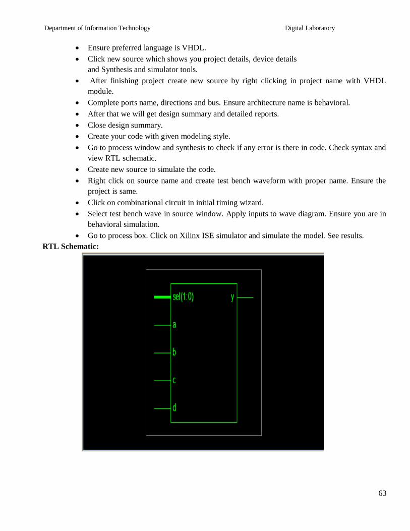
Department of Information Technology Digital Laboratory
64
Timing Diagram
FAQrsquos
1 What are the different kinds of data objects in VHDL code
Ans data object may be any value or number still some signal data objects and bit and bit_vector
types of these are available in VHDL STD_LOGIC and STD_LOGIC_VECTOR types are used
widely in programming
2 What do you mean by signal
Ans signal is a data object represents logic signals or wires in a circuit There are three places in
which signals can be declared in VHDL code in an entity declaration in the declarative section of
architecture and in declarative section of package
3 What are different signal types
Ans BIT BIT_VECTOR STD_LOGIC STD_LOGIC_VECTOR STD_ULOGIC SIGNED
UNSIGNED INTEGER ENUMERATION and BOOLEAN
4 What is an entity
Ans a circuit or sub circuit described with VHDL code is called a design entity
5 Explain structure of an entity
Ans it has two main parts the entity declaration which specifies the input and output signals for
entity and the architecture which gives circuit details
Department of Information Technology Digital Laboratory
65
6 How will you declare a package with component Explain structure
The general form of package declaration is as shown in diagram
PACKAGE package_name IS
[TYPE declarations]
[SIGNAL declarations]
[COMPONENT declarations]
END package_name
Entity
Declaration Architecture
Department of Information Technology Digital Laboratory
66
Regularity Content Viva-voce Timely
Submission Total
Dated Sign of
Subject
Teacher
2 4 2 2 10
Date of Performance Date of Completion
-------------------------------------------------------------------------------------------------------------------
Assignment No8
------------------------------------------------------------------------------------------------------------------
Title Full Adder using Behavioral and Structural modeling
------------------------------------------------------------------------------------------------------------------
Objective To learn structural modeling style Its uses and different types of declarations with some
different types of circuits Structure of VHDL program is well discussed with this modeling style
-------------------------------------------------------------------------------------------------------------------
Problem Statement Full adder using behavioral amp structural modeling
-----------------------------------------------------------------------------------------------------------------
Hardware Requirement - NA
----------------------------------------------------------------------------------------------------------------
Software Requirement Xilinx
------------------------------------------------------------------------------------------------------------------
Theory
Structural style-
A digital electronic system can be described as a module with inputs andor outputs The electrical values
on the outputs are same functions of the values of inputs The example of it is as shown The NAND gate
has 2ips AampB amp an output y Using VHDL terminology we call the NAND2 design entity amp the inputs
amp outputs are called ports 1 way of describing the function of NAND2 is to describe how it is composed
of sub modules AND amp INVERTER Each of the Sub modules is an instance of some entity amp ports of the
instances are connected using signals Structural modeling has a set of interconnected component
Structure can be used to create a very low level description of a circuit or a very high level description
Department of Information Technology Digital Laboratory
67
In a gate level description of a circuit for example components such as basic logic gates amp FFs might be
connected in some logical stricture to create the circuit This is what is often called a net list
Structure of structural modeling
Functional block diagram of Full Adder
architectureNetlistofHalf_Adderis
-- component with locals
componentMyXorport (A_XorB_Xor in BIT
Z_Xor out BIT)
end component
-- component with locals
componentMyAndport (A_AndB_And in BIT
Z_And out BIT)
end component
begin
Xor1 MyXorport map (X Y Sum)
-- instance with actuals
And1 MyAndport map (X Y Cout)
-- instance with actuals
end
Department of Information Technology Digital Laboratory
68
Function table of Full Adder
A B Cin SUM CARRY
0 0 0 0 0
0 0 1 1 0
0 1 0 1 0
0 1 1 0 1
1 0 0 1 0
1 0 1 0 1
1 1 0 0 1
1 1 1 1 1
Sum = Σm(1 2 4 7)
Carry= Σm(3 5 6 7)
Design steps
Click on Xilinx ISE 92i
Create New project from file menu Ensure top level source is HDL
Select family of devices (usually spartan2E or 3)
Ensure preferred language is VHDL
Click new source which shows you project details device details
and Synthesis and simulator tools
After finishing project create new source(full adder) by right clicking in project name with
VHDL module
Complete ports name directions and bus Ensure architecture name is behavioral
After that we will get design summary and detailed reports
Close design summary
Click new source which shows you project details device details
and Synthesis and simulator tools
After finishing project create new source(half adder) by right clicking in project name with
VHDL module
Complete ports name directions and bus Ensure architecture name is behavioral Names
should be same as previous inputs
Department of Information Technology Digital Laboratory
69
After that we will get design summary and detailed reports
Close design summary
Create your code for half adder with given modeling style
After that go to process window Click on design utilities
View HDL instantiation code of half adder
Copy component part of half adder in architecture block of full adder Copy instantiation
template twice after begin as we require two half adders to construct full adder (structural
modeling) Name them differently (eg ha1 or ha2)
Create signals as per the logic Complete code of full adder
Go to process window and synthesis to check if any error is there in code Check syntax and
view RTL schematic
Create new source to simulate the code
Right click on source name and create test bench waveform with proper name Ensure the
project is same
Click on combinational circuit in initial timing wizard
Select test bench wave in source window Apply inputs to wave diagram Ensure you are in
behavioral simulation
Go to process box Click on Xilinx ISE simulator and simulate the model See results
RTL Schematic
Timing Diagram
Department of Information Technology Digital Laboratory
70
INPUT
Three inputs A B Carry (previous)
OUTPUT
Two outputs Sum Carry
FAQrsquos
1 What do you mean by structural style
Ans in this type of code a circuit is described in hierarchical fashion by connecting together sub
circuits
2 Explain IF statement with example
Ans The general form of an IF statement is as follws
IF Sel=rsquo0rsquo THEN
Flt=x1
ELSE
Flt=x2
END IF
Department of Information Technology Digital Laboratory
71
3 Explain declaration and instantiation process in VHDL
Ans first declare a small vhdl code in formal way Eg half adder Define project name is full adder
And simply copy instantiation template in main source code Define how many times you want to
declare this template Give separate names for those
4 What is STD_LOGIC_VECTOR
Ans It is standard data object added to VHDL standard in IEEE 1164 It provides more flexibility
than the Bit type
5 Explain difference between concurrent and sequential statements
Ans Concurrent statements define interconnected processes and blocks that together describe a designrsquos
overall behavior or structure They can be grouped using block sstatement Groups of blocks can also be
partitioned into other blocks At this same level a VHDL component can be connected to define signals
within the blocks
It is a reference to an entity A process can be a single signal assignment statement or a series of
sequential statements (SS) Within a process procedures and functions can partition the sequential
statements
PRACTICE ASSIGNMENTS
1 Implement half adder using data flow modeling
2 Implement Full Adder using behavioral modeling
3 Implement 3 bit magnitude comparator using a 3 bit adder
4 Implement half sub tractor using data flow modeling
5 Write VHDL code for Full Subtractor
Department of Information Technology Digital Laboratory
72
Regularity Content Viva-voce Timely
Submission Total
Dated Sign of
Subject
Teacher
2 4 2 2 10
rsquozaDate of Performance Date of Completion
-------------------------------------------------------------------------------------------------------------------
Assignment No9
------------------------------------------------------------------------------------------------------------------
Title Simulation of 3 bit Connter using Behavioral modeling
------------------------------------------------------------------------------------------------------------------
Objective To learn behavioral modeling style Its uses and different types of declarations with some
different types of circuits Structure of VHDL program is well discussed with this modeling style
-------------------------------------------------------------------------------------------------------------------
Problem Statement 3 bit controlled up down synchronous counter with preset amp clear
-----------------------------------------------------------------------------------------------------------------
Hardware Requirement -NA
----------------------------------------------------------------------------------------------------------------
Software Requirement Xilinx
------------------------------------------------------------------------------------------------------------------
Theory
Behavioral style-
Highest level of abstraction supported in VHDL is called the behavior level of abstraction In it we have
for loop while loop If then else case ampvariable assignment The statements are enclosed in a PROCESS
block amp are executed sequentially
In it circuit is described in terms of its operation overtime
In behavioral description the concept of time may be expressed precisely with actual delays between
related events (such as the propagation delays within gates amp on wires) or it may be simply an ordering of
operation that are expressed sequentially (such as in a functional description of a FF)
Department of Information Technology Digital Laboratory
73
A behavioral design method defines a circuit in terms of text language rather than a schematic of
interconnected symbols
Behavioral design is a technology independent text based design that incorporates high level
functionality amp high level information flow
Structure of Behavioral modeling
Functional block diagram of 3 bit controlled up down synchronous counter with preset amp clear
Function table of 3 bit controlled up down synchronous counter with preset amp clear
Design steps
Click on Xilinx ISE 92i
Create New project from file menu Ensure top level source is HDL
Select family of devices (usually spartan2E or 3)
Ensure preferred language is VHDL
Click new source which shows you project details device details
and Synthesis and simulator tools
After finishing project create new source by right clicking in project name with VHDL
module
Complete ports name directions and bus Ensure architecture name is behavioral
After that we will get design summary and detailed reports
Close design summary
Create your code with given modeling style
Go to process window and synthesis to check if any error is there in code Check syntax
and view RTL schematic Create new source to simulate the code
Department of Information Technology Digital Laboratory
74
Right click on source name and create test bench waveform with proper name Ensure the
project is same
Click on combinational circuit in initial timing wizard
Select test bench wave in source window Apply inputs to wave diagram Ensure you are in
behavioral simulation
Go to process box Click on Xilinx ISE simulator and simulate the model
RTL Schematic
Timing Diagram
INPUT
Clock Preset Clear
OUTPUT
Three output lines
FAQrsquos
1 Explain the structure of behavioral modeling
2 What are the differences between behavioral and structural modeling
Ans Behavioral descriptionof a circuit is the highest level of abstraction in VHDL Here the
circuit is described in terms of it operation with respect to time All operations are in one level of
code The operations are described in a way that the designer of a sequential circuit infers a
register
Structural description on the other hand is a circuit description in terms of its components
it can either create a low level description much like a hierarchy in a block diagram Whenever
you see a component instantiated in a code that code employs structural description of the circuit
The components are connected in the form of a netlist This is for better manageability and
reusability
3 What are the differences between behavioral and data flow modeling
Department of Information Technology Digital Laboratory
75
Ans Behavioral ndash describes how the output is derived from the inputs using structured
statements
Dataflow ndash describes how the data flows from the inputs to the output most often
using NOT AND and OR operations
4 What do you mean by process statement
Ans The process statement begins with the PROCESS keyword followed by a parenthesized list
of signals called the sensitivity list It operates on selected and conditional statements
5 Explain syntax of process statement
Ans BEGIN
Process( sensitivity list)
END process
PRACTICE ASSIGNMENTS
1 Implement 3 bit asynchronous up counter using behavioral modeling
2 Implement 3 bit asynchronous down counter using behavioral modeling
3 Implement 3 bit synchronous down counter using behavioral modeling
End
Department of Information Technology Digital Laboratory
76
Pin Diagrams
7400 Quad 2-Input NAND Gate
7402 Quad 2-Input NOR Gate
7404 Not Gates
7408 Quad 2-Input AND Gates
7432 Quad 2-Input OR Gate
7486 Quad 2-Input Exclusive-OR Gate
Department of Information Technology Digital Laboratory
77
7483 4 bit Binary Adder
7490 Decade and Binary Counters
74138 38 Decoder
Department of Information Technology Digital Laboratory
78
74153 Dual 41 Multiplexer
74191 Synchronous UpDown 4 bit Binary counter with Mode Control
Department of Information Technology Digital Laboratory
79
74194 Universal Shift Register
7476 Dual Master-Slave J-K Flip-Flops
- Part B Sequence Generator using Shift Register IC 74194
-
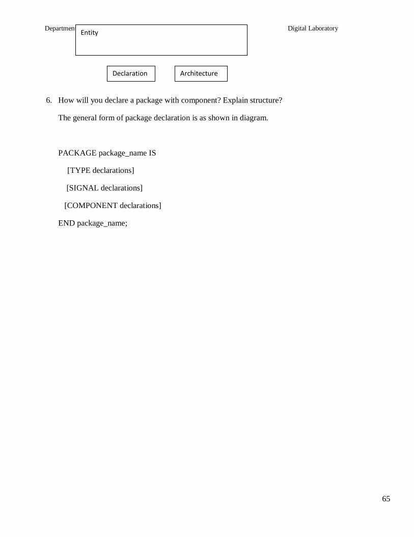
Department of Information Technology Digital Laboratory
65
6 How will you declare a package with component Explain structure
The general form of package declaration is as shown in diagram
PACKAGE package_name IS
[TYPE declarations]
[SIGNAL declarations]
[COMPONENT declarations]
END package_name
Entity
Declaration Architecture
Department of Information Technology Digital Laboratory
66
Regularity Content Viva-voce Timely
Submission Total
Dated Sign of
Subject
Teacher
2 4 2 2 10
Date of Performance Date of Completion
-------------------------------------------------------------------------------------------------------------------
Assignment No8
------------------------------------------------------------------------------------------------------------------
Title Full Adder using Behavioral and Structural modeling
------------------------------------------------------------------------------------------------------------------
Objective To learn structural modeling style Its uses and different types of declarations with some
different types of circuits Structure of VHDL program is well discussed with this modeling style
-------------------------------------------------------------------------------------------------------------------
Problem Statement Full adder using behavioral amp structural modeling
-----------------------------------------------------------------------------------------------------------------
Hardware Requirement - NA
----------------------------------------------------------------------------------------------------------------
Software Requirement Xilinx
------------------------------------------------------------------------------------------------------------------
Theory
Structural style-
A digital electronic system can be described as a module with inputs andor outputs The electrical values
on the outputs are same functions of the values of inputs The example of it is as shown The NAND gate
has 2ips AampB amp an output y Using VHDL terminology we call the NAND2 design entity amp the inputs
amp outputs are called ports 1 way of describing the function of NAND2 is to describe how it is composed
of sub modules AND amp INVERTER Each of the Sub modules is an instance of some entity amp ports of the
instances are connected using signals Structural modeling has a set of interconnected component
Structure can be used to create a very low level description of a circuit or a very high level description
Department of Information Technology Digital Laboratory
67
In a gate level description of a circuit for example components such as basic logic gates amp FFs might be
connected in some logical stricture to create the circuit This is what is often called a net list
Structure of structural modeling
Functional block diagram of Full Adder
architectureNetlistofHalf_Adderis
-- component with locals
componentMyXorport (A_XorB_Xor in BIT
Z_Xor out BIT)
end component
-- component with locals
componentMyAndport (A_AndB_And in BIT
Z_And out BIT)
end component
begin
Xor1 MyXorport map (X Y Sum)
-- instance with actuals
And1 MyAndport map (X Y Cout)
-- instance with actuals
end
Department of Information Technology Digital Laboratory
68
Function table of Full Adder
A B Cin SUM CARRY
0 0 0 0 0
0 0 1 1 0
0 1 0 1 0
0 1 1 0 1
1 0 0 1 0
1 0 1 0 1
1 1 0 0 1
1 1 1 1 1
Sum = Σm(1 2 4 7)
Carry= Σm(3 5 6 7)
Design steps
Click on Xilinx ISE 92i
Create New project from file menu Ensure top level source is HDL
Select family of devices (usually spartan2E or 3)
Ensure preferred language is VHDL
Click new source which shows you project details device details
and Synthesis and simulator tools
After finishing project create new source(full adder) by right clicking in project name with
VHDL module
Complete ports name directions and bus Ensure architecture name is behavioral
After that we will get design summary and detailed reports
Close design summary
Click new source which shows you project details device details
and Synthesis and simulator tools
After finishing project create new source(half adder) by right clicking in project name with
VHDL module
Complete ports name directions and bus Ensure architecture name is behavioral Names
should be same as previous inputs
Department of Information Technology Digital Laboratory
69
After that we will get design summary and detailed reports
Close design summary
Create your code for half adder with given modeling style
After that go to process window Click on design utilities
View HDL instantiation code of half adder
Copy component part of half adder in architecture block of full adder Copy instantiation
template twice after begin as we require two half adders to construct full adder (structural
modeling) Name them differently (eg ha1 or ha2)
Create signals as per the logic Complete code of full adder
Go to process window and synthesis to check if any error is there in code Check syntax and
view RTL schematic
Create new source to simulate the code
Right click on source name and create test bench waveform with proper name Ensure the
project is same
Click on combinational circuit in initial timing wizard
Select test bench wave in source window Apply inputs to wave diagram Ensure you are in
behavioral simulation
Go to process box Click on Xilinx ISE simulator and simulate the model See results
RTL Schematic
Timing Diagram
Department of Information Technology Digital Laboratory
70
INPUT
Three inputs A B Carry (previous)
OUTPUT
Two outputs Sum Carry
FAQrsquos
1 What do you mean by structural style
Ans in this type of code a circuit is described in hierarchical fashion by connecting together sub
circuits
2 Explain IF statement with example
Ans The general form of an IF statement is as follws
IF Sel=rsquo0rsquo THEN
Flt=x1
ELSE
Flt=x2
END IF
Department of Information Technology Digital Laboratory
71
3 Explain declaration and instantiation process in VHDL
Ans first declare a small vhdl code in formal way Eg half adder Define project name is full adder
And simply copy instantiation template in main source code Define how many times you want to
declare this template Give separate names for those
4 What is STD_LOGIC_VECTOR
Ans It is standard data object added to VHDL standard in IEEE 1164 It provides more flexibility
than the Bit type
5 Explain difference between concurrent and sequential statements
Ans Concurrent statements define interconnected processes and blocks that together describe a designrsquos
overall behavior or structure They can be grouped using block sstatement Groups of blocks can also be
partitioned into other blocks At this same level a VHDL component can be connected to define signals
within the blocks
It is a reference to an entity A process can be a single signal assignment statement or a series of
sequential statements (SS) Within a process procedures and functions can partition the sequential
statements
PRACTICE ASSIGNMENTS
1 Implement half adder using data flow modeling
2 Implement Full Adder using behavioral modeling
3 Implement 3 bit magnitude comparator using a 3 bit adder
4 Implement half sub tractor using data flow modeling
5 Write VHDL code for Full Subtractor
Department of Information Technology Digital Laboratory
72
Regularity Content Viva-voce Timely
Submission Total
Dated Sign of
Subject
Teacher
2 4 2 2 10
rsquozaDate of Performance Date of Completion
-------------------------------------------------------------------------------------------------------------------
Assignment No9
------------------------------------------------------------------------------------------------------------------
Title Simulation of 3 bit Connter using Behavioral modeling
------------------------------------------------------------------------------------------------------------------
Objective To learn behavioral modeling style Its uses and different types of declarations with some
different types of circuits Structure of VHDL program is well discussed with this modeling style
-------------------------------------------------------------------------------------------------------------------
Problem Statement 3 bit controlled up down synchronous counter with preset amp clear
-----------------------------------------------------------------------------------------------------------------
Hardware Requirement -NA
----------------------------------------------------------------------------------------------------------------
Software Requirement Xilinx
------------------------------------------------------------------------------------------------------------------
Theory
Behavioral style-
Highest level of abstraction supported in VHDL is called the behavior level of abstraction In it we have
for loop while loop If then else case ampvariable assignment The statements are enclosed in a PROCESS
block amp are executed sequentially
In it circuit is described in terms of its operation overtime
In behavioral description the concept of time may be expressed precisely with actual delays between
related events (such as the propagation delays within gates amp on wires) or it may be simply an ordering of
operation that are expressed sequentially (such as in a functional description of a FF)
Department of Information Technology Digital Laboratory
73
A behavioral design method defines a circuit in terms of text language rather than a schematic of
interconnected symbols
Behavioral design is a technology independent text based design that incorporates high level
functionality amp high level information flow
Structure of Behavioral modeling
Functional block diagram of 3 bit controlled up down synchronous counter with preset amp clear
Function table of 3 bit controlled up down synchronous counter with preset amp clear
Design steps
Click on Xilinx ISE 92i
Create New project from file menu Ensure top level source is HDL
Select family of devices (usually spartan2E or 3)
Ensure preferred language is VHDL
Click new source which shows you project details device details
and Synthesis and simulator tools
After finishing project create new source by right clicking in project name with VHDL
module
Complete ports name directions and bus Ensure architecture name is behavioral
After that we will get design summary and detailed reports
Close design summary
Create your code with given modeling style
Go to process window and synthesis to check if any error is there in code Check syntax
and view RTL schematic Create new source to simulate the code
Department of Information Technology Digital Laboratory
74
Right click on source name and create test bench waveform with proper name Ensure the
project is same
Click on combinational circuit in initial timing wizard
Select test bench wave in source window Apply inputs to wave diagram Ensure you are in
behavioral simulation
Go to process box Click on Xilinx ISE simulator and simulate the model
RTL Schematic
Timing Diagram
INPUT
Clock Preset Clear
OUTPUT
Three output lines
FAQrsquos
1 Explain the structure of behavioral modeling
2 What are the differences between behavioral and structural modeling
Ans Behavioral descriptionof a circuit is the highest level of abstraction in VHDL Here the
circuit is described in terms of it operation with respect to time All operations are in one level of
code The operations are described in a way that the designer of a sequential circuit infers a
register
Structural description on the other hand is a circuit description in terms of its components
it can either create a low level description much like a hierarchy in a block diagram Whenever
you see a component instantiated in a code that code employs structural description of the circuit
The components are connected in the form of a netlist This is for better manageability and
reusability
3 What are the differences between behavioral and data flow modeling
Department of Information Technology Digital Laboratory
75
Ans Behavioral ndash describes how the output is derived from the inputs using structured
statements
Dataflow ndash describes how the data flows from the inputs to the output most often
using NOT AND and OR operations
4 What do you mean by process statement
Ans The process statement begins with the PROCESS keyword followed by a parenthesized list
of signals called the sensitivity list It operates on selected and conditional statements
5 Explain syntax of process statement
Ans BEGIN
Process( sensitivity list)
END process
PRACTICE ASSIGNMENTS
1 Implement 3 bit asynchronous up counter using behavioral modeling
2 Implement 3 bit asynchronous down counter using behavioral modeling
3 Implement 3 bit synchronous down counter using behavioral modeling
End
Department of Information Technology Digital Laboratory
76
Pin Diagrams
7400 Quad 2-Input NAND Gate
7402 Quad 2-Input NOR Gate
7404 Not Gates
7408 Quad 2-Input AND Gates
7432 Quad 2-Input OR Gate
7486 Quad 2-Input Exclusive-OR Gate
Department of Information Technology Digital Laboratory
77
7483 4 bit Binary Adder
7490 Decade and Binary Counters
74138 38 Decoder
Department of Information Technology Digital Laboratory
78
74153 Dual 41 Multiplexer
74191 Synchronous UpDown 4 bit Binary counter with Mode Control
Department of Information Technology Digital Laboratory
79
74194 Universal Shift Register
7476 Dual Master-Slave J-K Flip-Flops
- Part B Sequence Generator using Shift Register IC 74194
-
Department of Information Technology Digital Laboratory
66
Regularity Content Viva-voce Timely
Submission Total
Dated Sign of
Subject
Teacher
2 4 2 2 10
Date of Performance Date of Completion
-------------------------------------------------------------------------------------------------------------------
Assignment No8
------------------------------------------------------------------------------------------------------------------
Title Full Adder using Behavioral and Structural modeling
------------------------------------------------------------------------------------------------------------------
Objective To learn structural modeling style Its uses and different types of declarations with some
different types of circuits Structure of VHDL program is well discussed with this modeling style
-------------------------------------------------------------------------------------------------------------------
Problem Statement Full adder using behavioral amp structural modeling
-----------------------------------------------------------------------------------------------------------------
Hardware Requirement - NA
----------------------------------------------------------------------------------------------------------------
Software Requirement Xilinx
------------------------------------------------------------------------------------------------------------------
Theory
Structural style-
A digital electronic system can be described as a module with inputs andor outputs The electrical values
on the outputs are same functions of the values of inputs The example of it is as shown The NAND gate
has 2ips AampB amp an output y Using VHDL terminology we call the NAND2 design entity amp the inputs
amp outputs are called ports 1 way of describing the function of NAND2 is to describe how it is composed
of sub modules AND amp INVERTER Each of the Sub modules is an instance of some entity amp ports of the
instances are connected using signals Structural modeling has a set of interconnected component
Structure can be used to create a very low level description of a circuit or a very high level description
Department of Information Technology Digital Laboratory
67
In a gate level description of a circuit for example components such as basic logic gates amp FFs might be
connected in some logical stricture to create the circuit This is what is often called a net list
Structure of structural modeling
Functional block diagram of Full Adder
architectureNetlistofHalf_Adderis
-- component with locals
componentMyXorport (A_XorB_Xor in BIT
Z_Xor out BIT)
end component
-- component with locals
componentMyAndport (A_AndB_And in BIT
Z_And out BIT)
end component
begin
Xor1 MyXorport map (X Y Sum)
-- instance with actuals
And1 MyAndport map (X Y Cout)
-- instance with actuals
end
Department of Information Technology Digital Laboratory
68
Function table of Full Adder
A B Cin SUM CARRY
0 0 0 0 0
0 0 1 1 0
0 1 0 1 0
0 1 1 0 1
1 0 0 1 0
1 0 1 0 1
1 1 0 0 1
1 1 1 1 1
Sum = Σm(1 2 4 7)
Carry= Σm(3 5 6 7)
Design steps
Click on Xilinx ISE 92i
Create New project from file menu Ensure top level source is HDL
Select family of devices (usually spartan2E or 3)
Ensure preferred language is VHDL
Click new source which shows you project details device details
and Synthesis and simulator tools
After finishing project create new source(full adder) by right clicking in project name with
VHDL module
Complete ports name directions and bus Ensure architecture name is behavioral
After that we will get design summary and detailed reports
Close design summary
Click new source which shows you project details device details
and Synthesis and simulator tools
After finishing project create new source(half adder) by right clicking in project name with
VHDL module
Complete ports name directions and bus Ensure architecture name is behavioral Names
should be same as previous inputs
Department of Information Technology Digital Laboratory
69
After that we will get design summary and detailed reports
Close design summary
Create your code for half adder with given modeling style
After that go to process window Click on design utilities
View HDL instantiation code of half adder
Copy component part of half adder in architecture block of full adder Copy instantiation
template twice after begin as we require two half adders to construct full adder (structural
modeling) Name them differently (eg ha1 or ha2)
Create signals as per the logic Complete code of full adder
Go to process window and synthesis to check if any error is there in code Check syntax and
view RTL schematic
Create new source to simulate the code
Right click on source name and create test bench waveform with proper name Ensure the
project is same
Click on combinational circuit in initial timing wizard
Select test bench wave in source window Apply inputs to wave diagram Ensure you are in
behavioral simulation
Go to process box Click on Xilinx ISE simulator and simulate the model See results
RTL Schematic
Timing Diagram
Department of Information Technology Digital Laboratory
70
INPUT
Three inputs A B Carry (previous)
OUTPUT
Two outputs Sum Carry
FAQrsquos
1 What do you mean by structural style
Ans in this type of code a circuit is described in hierarchical fashion by connecting together sub
circuits
2 Explain IF statement with example
Ans The general form of an IF statement is as follws
IF Sel=rsquo0rsquo THEN
Flt=x1
ELSE
Flt=x2
END IF
Department of Information Technology Digital Laboratory
71
3 Explain declaration and instantiation process in VHDL
Ans first declare a small vhdl code in formal way Eg half adder Define project name is full adder
And simply copy instantiation template in main source code Define how many times you want to
declare this template Give separate names for those
4 What is STD_LOGIC_VECTOR
Ans It is standard data object added to VHDL standard in IEEE 1164 It provides more flexibility
than the Bit type
5 Explain difference between concurrent and sequential statements
Ans Concurrent statements define interconnected processes and blocks that together describe a designrsquos
overall behavior or structure They can be grouped using block sstatement Groups of blocks can also be
partitioned into other blocks At this same level a VHDL component can be connected to define signals
within the blocks
It is a reference to an entity A process can be a single signal assignment statement or a series of
sequential statements (SS) Within a process procedures and functions can partition the sequential
statements
PRACTICE ASSIGNMENTS
1 Implement half adder using data flow modeling
2 Implement Full Adder using behavioral modeling
3 Implement 3 bit magnitude comparator using a 3 bit adder
4 Implement half sub tractor using data flow modeling
5 Write VHDL code for Full Subtractor
Department of Information Technology Digital Laboratory
72
Regularity Content Viva-voce Timely
Submission Total
Dated Sign of
Subject
Teacher
2 4 2 2 10
rsquozaDate of Performance Date of Completion
-------------------------------------------------------------------------------------------------------------------
Assignment No9
------------------------------------------------------------------------------------------------------------------
Title Simulation of 3 bit Connter using Behavioral modeling
------------------------------------------------------------------------------------------------------------------
Objective To learn behavioral modeling style Its uses and different types of declarations with some
different types of circuits Structure of VHDL program is well discussed with this modeling style
-------------------------------------------------------------------------------------------------------------------
Problem Statement 3 bit controlled up down synchronous counter with preset amp clear
-----------------------------------------------------------------------------------------------------------------
Hardware Requirement -NA
----------------------------------------------------------------------------------------------------------------
Software Requirement Xilinx
------------------------------------------------------------------------------------------------------------------
Theory
Behavioral style-
Highest level of abstraction supported in VHDL is called the behavior level of abstraction In it we have
for loop while loop If then else case ampvariable assignment The statements are enclosed in a PROCESS
block amp are executed sequentially
In it circuit is described in terms of its operation overtime
In behavioral description the concept of time may be expressed precisely with actual delays between
related events (such as the propagation delays within gates amp on wires) or it may be simply an ordering of
operation that are expressed sequentially (such as in a functional description of a FF)
Department of Information Technology Digital Laboratory
73
A behavioral design method defines a circuit in terms of text language rather than a schematic of
interconnected symbols
Behavioral design is a technology independent text based design that incorporates high level
functionality amp high level information flow
Structure of Behavioral modeling
Functional block diagram of 3 bit controlled up down synchronous counter with preset amp clear
Function table of 3 bit controlled up down synchronous counter with preset amp clear
Design steps
Click on Xilinx ISE 92i
Create New project from file menu Ensure top level source is HDL
Select family of devices (usually spartan2E or 3)
Ensure preferred language is VHDL
Click new source which shows you project details device details
and Synthesis and simulator tools
After finishing project create new source by right clicking in project name with VHDL
module
Complete ports name directions and bus Ensure architecture name is behavioral
After that we will get design summary and detailed reports
Close design summary
Create your code with given modeling style
Go to process window and synthesis to check if any error is there in code Check syntax
and view RTL schematic Create new source to simulate the code
Department of Information Technology Digital Laboratory
74
Right click on source name and create test bench waveform with proper name Ensure the
project is same
Click on combinational circuit in initial timing wizard
Select test bench wave in source window Apply inputs to wave diagram Ensure you are in
behavioral simulation
Go to process box Click on Xilinx ISE simulator and simulate the model
RTL Schematic
Timing Diagram
INPUT
Clock Preset Clear
OUTPUT
Three output lines
FAQrsquos
1 Explain the structure of behavioral modeling
2 What are the differences between behavioral and structural modeling
Ans Behavioral descriptionof a circuit is the highest level of abstraction in VHDL Here the
circuit is described in terms of it operation with respect to time All operations are in one level of
code The operations are described in a way that the designer of a sequential circuit infers a
register
Structural description on the other hand is a circuit description in terms of its components
it can either create a low level description much like a hierarchy in a block diagram Whenever
you see a component instantiated in a code that code employs structural description of the circuit
The components are connected in the form of a netlist This is for better manageability and
reusability
3 What are the differences between behavioral and data flow modeling
Department of Information Technology Digital Laboratory
75
Ans Behavioral ndash describes how the output is derived from the inputs using structured
statements
Dataflow ndash describes how the data flows from the inputs to the output most often
using NOT AND and OR operations
4 What do you mean by process statement
Ans The process statement begins with the PROCESS keyword followed by a parenthesized list
of signals called the sensitivity list It operates on selected and conditional statements
5 Explain syntax of process statement
Ans BEGIN
Process( sensitivity list)
END process
PRACTICE ASSIGNMENTS
1 Implement 3 bit asynchronous up counter using behavioral modeling
2 Implement 3 bit asynchronous down counter using behavioral modeling
3 Implement 3 bit synchronous down counter using behavioral modeling
End
Department of Information Technology Digital Laboratory
76
Pin Diagrams
7400 Quad 2-Input NAND Gate
7402 Quad 2-Input NOR Gate
7404 Not Gates
7408 Quad 2-Input AND Gates
7432 Quad 2-Input OR Gate
7486 Quad 2-Input Exclusive-OR Gate
Department of Information Technology Digital Laboratory
77
7483 4 bit Binary Adder
7490 Decade and Binary Counters
74138 38 Decoder
Department of Information Technology Digital Laboratory
78
74153 Dual 41 Multiplexer
74191 Synchronous UpDown 4 bit Binary counter with Mode Control
Department of Information Technology Digital Laboratory
79
74194 Universal Shift Register
7476 Dual Master-Slave J-K Flip-Flops
- Part B Sequence Generator using Shift Register IC 74194
-
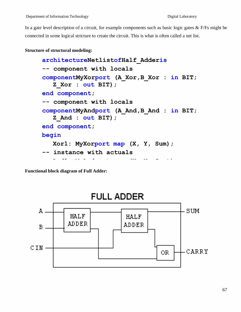
Department of Information Technology Digital Laboratory
71
3 Explain declaration and instantiation process in VHDL
Ans first declare a small vhdl code in formal way Eg half adder Define project name is full adder
And simply copy instantiation template in main source code Define how many times you want to
declare this template Give separate names for those
4 What is STD_LOGIC_VECTOR
Ans It is standard data object added to VHDL standard in IEEE 1164 It provides more flexibility
than the Bit type
5 Explain difference between concurrent and sequential statements
Ans Concurrent statements define interconnected processes and blocks that together describe a designrsquos
overall behavior or structure They can be grouped using block sstatement Groups of blocks can also be
partitioned into other blocks At this same level a VHDL component can be connected to define signals
within the blocks
It is a reference to an entity A process can be a single signal assignment statement or a series of
sequential statements (SS) Within a process procedures and functions can partition the sequential
statements
PRACTICE ASSIGNMENTS
1 Implement half adder using data flow modeling
2 Implement Full Adder using behavioral modeling
3 Implement 3 bit magnitude comparator using a 3 bit adder
4 Implement half sub tractor using data flow modeling
5 Write VHDL code for Full Subtractor
Department of Information Technology Digital Laboratory
72
Regularity Content Viva-voce Timely
Submission Total
Dated Sign of
Subject
Teacher
2 4 2 2 10
rsquozaDate of Performance Date of Completion
-------------------------------------------------------------------------------------------------------------------
Assignment No9
------------------------------------------------------------------------------------------------------------------
Title Simulation of 3 bit Connter using Behavioral modeling
------------------------------------------------------------------------------------------------------------------
Objective To learn behavioral modeling style Its uses and different types of declarations with some
different types of circuits Structure of VHDL program is well discussed with this modeling style
-------------------------------------------------------------------------------------------------------------------
Problem Statement 3 bit controlled up down synchronous counter with preset amp clear
-----------------------------------------------------------------------------------------------------------------
Hardware Requirement -NA
----------------------------------------------------------------------------------------------------------------
Software Requirement Xilinx
------------------------------------------------------------------------------------------------------------------
Theory
Behavioral style-
Highest level of abstraction supported in VHDL is called the behavior level of abstraction In it we have
for loop while loop If then else case ampvariable assignment The statements are enclosed in a PROCESS
block amp are executed sequentially
In it circuit is described in terms of its operation overtime
In behavioral description the concept of time may be expressed precisely with actual delays between
related events (such as the propagation delays within gates amp on wires) or it may be simply an ordering of
operation that are expressed sequentially (such as in a functional description of a FF)
Department of Information Technology Digital Laboratory
73
A behavioral design method defines a circuit in terms of text language rather than a schematic of
interconnected symbols
Behavioral design is a technology independent text based design that incorporates high level
functionality amp high level information flow
Structure of Behavioral modeling
Functional block diagram of 3 bit controlled up down synchronous counter with preset amp clear
Function table of 3 bit controlled up down synchronous counter with preset amp clear
Design steps
Click on Xilinx ISE 92i
Create New project from file menu Ensure top level source is HDL
Select family of devices (usually spartan2E or 3)
Ensure preferred language is VHDL
Click new source which shows you project details device details
and Synthesis and simulator tools
After finishing project create new source by right clicking in project name with VHDL
module
Complete ports name directions and bus Ensure architecture name is behavioral
After that we will get design summary and detailed reports
Close design summary
Create your code with given modeling style
Go to process window and synthesis to check if any error is there in code Check syntax
and view RTL schematic Create new source to simulate the code
Department of Information Technology Digital Laboratory
74
Right click on source name and create test bench waveform with proper name Ensure the
project is same
Click on combinational circuit in initial timing wizard
Select test bench wave in source window Apply inputs to wave diagram Ensure you are in
behavioral simulation
Go to process box Click on Xilinx ISE simulator and simulate the model
RTL Schematic
Timing Diagram
INPUT
Clock Preset Clear
OUTPUT
Three output lines
FAQrsquos
1 Explain the structure of behavioral modeling
2 What are the differences between behavioral and structural modeling
Ans Behavioral descriptionof a circuit is the highest level of abstraction in VHDL Here the
circuit is described in terms of it operation with respect to time All operations are in one level of
code The operations are described in a way that the designer of a sequential circuit infers a
register
Structural description on the other hand is a circuit description in terms of its components
it can either create a low level description much like a hierarchy in a block diagram Whenever
you see a component instantiated in a code that code employs structural description of the circuit
The components are connected in the form of a netlist This is for better manageability and
reusability
3 What are the differences between behavioral and data flow modeling
Department of Information Technology Digital Laboratory
75
Ans Behavioral ndash describes how the output is derived from the inputs using structured
statements
Dataflow ndash describes how the data flows from the inputs to the output most often
using NOT AND and OR operations
4 What do you mean by process statement
Ans The process statement begins with the PROCESS keyword followed by a parenthesized list
of signals called the sensitivity list It operates on selected and conditional statements
5 Explain syntax of process statement
Ans BEGIN
Process( sensitivity list)
END process
PRACTICE ASSIGNMENTS
1 Implement 3 bit asynchronous up counter using behavioral modeling
2 Implement 3 bit asynchronous down counter using behavioral modeling
3 Implement 3 bit synchronous down counter using behavioral modeling
End
Department of Information Technology Digital Laboratory
76
Pin Diagrams
7400 Quad 2-Input NAND Gate
7402 Quad 2-Input NOR Gate
7404 Not Gates
7408 Quad 2-Input AND Gates
7432 Quad 2-Input OR Gate
7486 Quad 2-Input Exclusive-OR Gate
Department of Information Technology Digital Laboratory
77
7483 4 bit Binary Adder
7490 Decade and Binary Counters
74138 38 Decoder
Department of Information Technology Digital Laboratory
78
74153 Dual 41 Multiplexer
74191 Synchronous UpDown 4 bit Binary counter with Mode Control
Department of Information Technology Digital Laboratory
79
74194 Universal Shift Register
7476 Dual Master-Slave J-K Flip-Flops
- Part B Sequence Generator using Shift Register IC 74194
-
Department of Information Technology Digital Laboratory
72
Regularity Content Viva-voce Timely
Submission Total
Dated Sign of
Subject
Teacher
2 4 2 2 10
rsquozaDate of Performance Date of Completion
-------------------------------------------------------------------------------------------------------------------
Assignment No9
------------------------------------------------------------------------------------------------------------------
Title Simulation of 3 bit Connter using Behavioral modeling
------------------------------------------------------------------------------------------------------------------
Objective To learn behavioral modeling style Its uses and different types of declarations with some
different types of circuits Structure of VHDL program is well discussed with this modeling style
-------------------------------------------------------------------------------------------------------------------
Problem Statement 3 bit controlled up down synchronous counter with preset amp clear
-----------------------------------------------------------------------------------------------------------------
Hardware Requirement -NA
----------------------------------------------------------------------------------------------------------------
Software Requirement Xilinx
------------------------------------------------------------------------------------------------------------------
Theory
Behavioral style-
Highest level of abstraction supported in VHDL is called the behavior level of abstraction In it we have
for loop while loop If then else case ampvariable assignment The statements are enclosed in a PROCESS
block amp are executed sequentially
In it circuit is described in terms of its operation overtime
In behavioral description the concept of time may be expressed precisely with actual delays between
related events (such as the propagation delays within gates amp on wires) or it may be simply an ordering of
operation that are expressed sequentially (such as in a functional description of a FF)
Department of Information Technology Digital Laboratory
73
A behavioral design method defines a circuit in terms of text language rather than a schematic of
interconnected symbols
Behavioral design is a technology independent text based design that incorporates high level
functionality amp high level information flow
Structure of Behavioral modeling
Functional block diagram of 3 bit controlled up down synchronous counter with preset amp clear
Function table of 3 bit controlled up down synchronous counter with preset amp clear
Design steps
Click on Xilinx ISE 92i
Create New project from file menu Ensure top level source is HDL
Select family of devices (usually spartan2E or 3)
Ensure preferred language is VHDL
Click new source which shows you project details device details
and Synthesis and simulator tools
After finishing project create new source by right clicking in project name with VHDL
module
Complete ports name directions and bus Ensure architecture name is behavioral
After that we will get design summary and detailed reports
Close design summary
Create your code with given modeling style
Go to process window and synthesis to check if any error is there in code Check syntax
and view RTL schematic Create new source to simulate the code
Department of Information Technology Digital Laboratory
74
Right click on source name and create test bench waveform with proper name Ensure the
project is same
Click on combinational circuit in initial timing wizard
Select test bench wave in source window Apply inputs to wave diagram Ensure you are in
behavioral simulation
Go to process box Click on Xilinx ISE simulator and simulate the model
RTL Schematic
Timing Diagram
INPUT
Clock Preset Clear
OUTPUT
Three output lines
FAQrsquos
1 Explain the structure of behavioral modeling
2 What are the differences between behavioral and structural modeling
Ans Behavioral descriptionof a circuit is the highest level of abstraction in VHDL Here the
circuit is described in terms of it operation with respect to time All operations are in one level of
code The operations are described in a way that the designer of a sequential circuit infers a
register
Structural description on the other hand is a circuit description in terms of its components
it can either create a low level description much like a hierarchy in a block diagram Whenever
you see a component instantiated in a code that code employs structural description of the circuit
The components are connected in the form of a netlist This is for better manageability and
reusability
3 What are the differences between behavioral and data flow modeling
Department of Information Technology Digital Laboratory
75
Ans Behavioral ndash describes how the output is derived from the inputs using structured
statements
Dataflow ndash describes how the data flows from the inputs to the output most often
using NOT AND and OR operations
4 What do you mean by process statement
Ans The process statement begins with the PROCESS keyword followed by a parenthesized list
of signals called the sensitivity list It operates on selected and conditional statements
5 Explain syntax of process statement
Ans BEGIN
Process( sensitivity list)
END process
PRACTICE ASSIGNMENTS
1 Implement 3 bit asynchronous up counter using behavioral modeling
2 Implement 3 bit asynchronous down counter using behavioral modeling
3 Implement 3 bit synchronous down counter using behavioral modeling
End
Department of Information Technology Digital Laboratory
76
Pin Diagrams
7400 Quad 2-Input NAND Gate
7402 Quad 2-Input NOR Gate
7404 Not Gates
7408 Quad 2-Input AND Gates
7432 Quad 2-Input OR Gate
7486 Quad 2-Input Exclusive-OR Gate
Department of Information Technology Digital Laboratory
77
7483 4 bit Binary Adder
7490 Decade and Binary Counters
74138 38 Decoder
Department of Information Technology Digital Laboratory
78
74153 Dual 41 Multiplexer
74191 Synchronous UpDown 4 bit Binary counter with Mode Control
Department of Information Technology Digital Laboratory
79
74194 Universal Shift Register
7476 Dual Master-Slave J-K Flip-Flops
- Part B Sequence Generator using Shift Register IC 74194
-
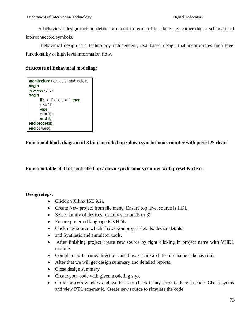
Department of Information Technology Digital Laboratory
76
Pin Diagrams
7400 Quad 2-Input NAND Gate
7402 Quad 2-Input NOR Gate
7404 Not Gates
7408 Quad 2-Input AND Gates
7432 Quad 2-Input OR Gate
7486 Quad 2-Input Exclusive-OR Gate
Department of Information Technology Digital Laboratory
77
7483 4 bit Binary Adder
7490 Decade and Binary Counters
74138 38 Decoder
Department of Information Technology Digital Laboratory
78
74153 Dual 41 Multiplexer
74191 Synchronous UpDown 4 bit Binary counter with Mode Control
Department of Information Technology Digital Laboratory
79
74194 Universal Shift Register
7476 Dual Master-Slave J-K Flip-Flops
- Part B Sequence Generator using Shift Register IC 74194
-
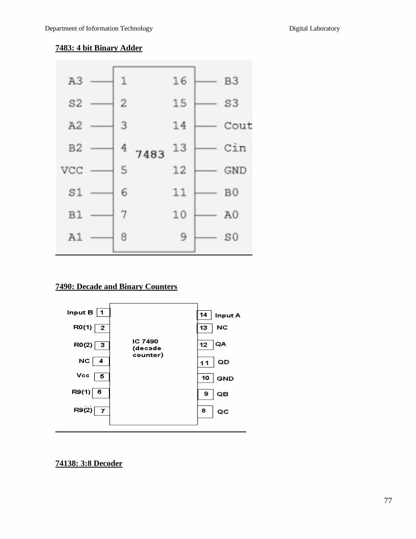
Department of Information Technology Digital Laboratory
77
7483 4 bit Binary Adder
7490 Decade and Binary Counters
74138 38 Decoder
Department of Information Technology Digital Laboratory
78
74153 Dual 41 Multiplexer
74191 Synchronous UpDown 4 bit Binary counter with Mode Control
Department of Information Technology Digital Laboratory
79
74194 Universal Shift Register
7476 Dual Master-Slave J-K Flip-Flops
- Part B Sequence Generator using Shift Register IC 74194
-
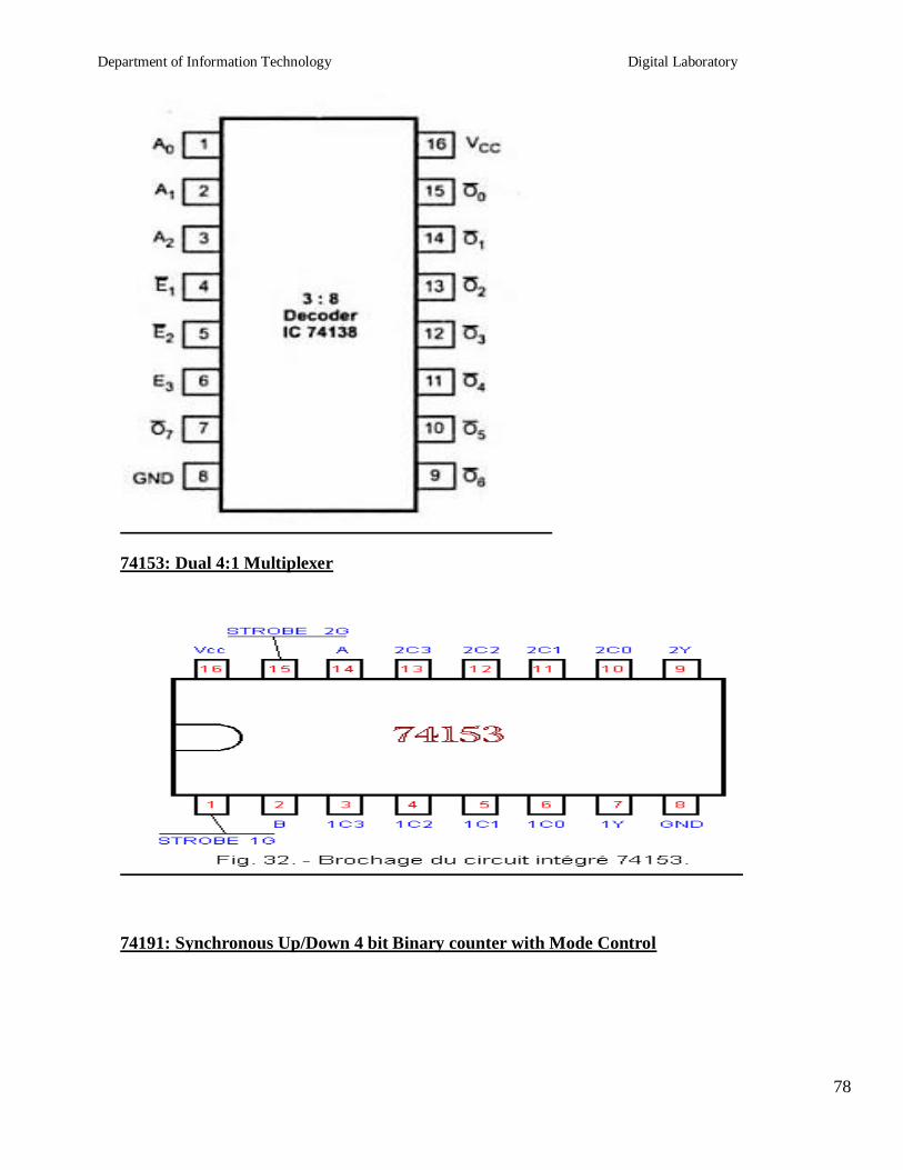
Department of Information Technology Digital Laboratory
79
74194 Universal Shift Register
7476 Dual Master-Slave J-K Flip-Flops
- Part B Sequence Generator using Shift Register IC 74194
-