m. neklyudova, a. k. erdamar, l. vicarelli, s. j. heerema
TRANSCRIPT

Through-membrane electron-beam lithography for ultrathin membrane applicationsM. Neklyudova, A. K. Erdamar, L. Vicarelli, S. J. Heerema, T. Rehfeldt, G. Pandraud, Z. Kolahdouz, C. Dekker,and H. W. Zandbergen
Citation: Appl. Phys. Lett. 111, 063105 (2017); doi: 10.1063/1.4986991View online: http://dx.doi.org/10.1063/1.4986991View Table of Contents: http://aip.scitation.org/toc/apl/111/6Published by the American Institute of Physics
Articles you may be interested in Native-oxide limited cross-plane thermal transport in suspended silicon membranes revealed by scanningthermal microscopyApplied Physics Letters 111, 063106 (2017); 10.1063/1.4997914
Effect of oxygen plasma on nanomechanical silicon nitride resonatorsApplied Physics Letters 111, 063103 (2017); 10.1063/1.4989775
The limit of quantum cascade detectors: A single period deviceApplied Physics Letters 111, 061107 (2017); 10.1063/1.4985711
Development of simple high-resolution embedded printing for transparent metal grid conductorsApplied Physics Letters 111, 063107 (2017); 10.1063/1.4997927
Enhanced ferro- and piezoelectric performances through interface control in BiFe0.99W0.01O3/BiFe0.95Mn0.05O3/BiFe0.99W0.01O3 thin filmApplied Physics Letters 111, 062902 (2017); 10.1063/1.4998162
Electron microscopy with high accuracy and precision at atomic resolution: In-situ observation of a dielectriccrystal under electric fieldApplied Physics Letters 111, 062904 (2017); 10.1063/1.4986361

Through-membrane electron-beam lithography for ultrathin membraneapplications
M. Neklyudova,1 A. K. Erdamar,1 L. Vicarelli,1 S. J. Heerema,1 T. Rehfeldt,1 G. Pandraud,2
Z. Kolahdouz,1 C. Dekker,1 and H. W. Zandbergen1,a)
1Kavli Institute of Nanoscience, Delft University of Technology, Delft 2628CJ, the Netherlands2Else Kooi Laboratory, Delft University of Technology, Delft 2628CT, the Netherlands
(Received 8 June 2017; accepted 28 July 2017; published online 9 August 2017)
We present a technique to fabricate ultrathin (down to 20 nm) uniform electron transparent windows
at dedicated locations in a SiN membrane for in situ transmission electron microscopy experiments.
An electron-beam (e-beam) resist is spray-coated on the backside of the membrane in a KOH-
etched cavity in silicon which is patterned using through-membrane electron-beam lithography.
This is a controlled way to make transparent windows in membranes, whilst the topside of the mem-
brane remains undamaged and retains its flatness. Our approach was optimized for MEMS-based
heating chips but can be applied to any chip design. We show two different applications of this tech-
nique for (1) fabrication of a nanogap electrode by means of electromigration in thin free-standing
metal films and (2) making low-noise graphene nanopore devices. Published by AIP Publishing.[http://dx.doi.org/10.1063/1.4986991]
For in situ TEM heating and biasing experiments, one
needs chips containing less than 20 nm-thick amorphous
membrane windows to obtain a good electron transparency.1,2
Once the freestanding area of the membrane needs to be
larger than several microns, or when the membrane design is
more complex (i.e., includes metal electrodes), it becomes
very difficult to maintain the membranes intact. One way to
obtain these thin membrane windows is to pattern a mask
(such as a resist layer) on the topside of the SiN and etch the
material down to the Si, followed by deposition of a thin
layer of SiN using low pressure chemical vapor deposition
(LPCVD). This approach has one big disadvantage: the thin
windows are formed at the bottom of the thick SiN membrane
(see Fig. S1 in the supplementary material), meaning that the
SiN window is in a deep cavity compared to the top surface
of the membrane. Such deep cavity-shaped membrane win-
dows are very inconvenient for various measurements, such
as liquid in situ TEM experiments. Also, additional deposi-
tion of electrical contacts for biasing in situ TEM experi-
ments on these recessed surfaces is impossible. To address
such issues, we have developed a technique where the SiN is
locally removed from the backside, such that the topside of
the membrane remains undamaged.
Performing electron-beam lithography (EBL) from the
backside of the membrane is not trivial with conventional
lithography systems since it stands at the bottom of a
300–500 lm-deep KOH-etched cavity. The resist mask should
cover the surface that is going to be patterned and with the
distance of less than 100 lm to the lens of the EBL device to
avoid defocusing issues.
In this paper, we show that the e-beam resist, which is
spray coated on the backside of the SiN membrane, can be
exposed with an e-beam from the topside and, therefore,
through the membrane and the structures on top of it. In this
way, the defocusing problem is solved, since the lens will be
in close enough proximity to the resist layer. After explana-
tion of the full procedure, we present two examples of appli-
cations of this approach.
Fabrication of the MEMS-based heaters consists of sev-
eral steps. First, we start with 300–500 lm thick Si wafers
and deposit 200 nm-thick SiN by the low pressure chemical
vapor deposition (LPCVD) technique as an isolation layer
between the metal and the Si substrate. Heater coils are
made of Tantalum (Ta)/Platinum (Pt) metal layers with 20/
180 nm thicknesses, respectively, deposited by e-beam evap-
oration and etched by ion etching. After the second deposi-
tion of 200 nm-thick LPCVD SiN, the heater is embedded in
a total 400 nm-thick SiN. The free-standing SiN membranes
are obtained by KOH-etching of Si.
Next, e-beam resist (PMMA:PGMEA:MEK) is sprayed
in multiple steps on the backside of the chips with an
EVG101 spray-coater. The main challenge of this method is
to obtain uniform resist coverage on the backside of SiN
membranes due to high topography of the 300–500 lm-deep
KOH-etched cavity (shown schematically in Fig. 1). The opti-
mized recipe results in a 12 lm-thick PMMA resist layer. The
resist is exposed from the topside of the chip by 100 kV elec-
trons penetrating through the 400 nm-thick SiN membrane
FIG. 1. Schematic illustration (not to scale) of the fabrication process of
backside opening by excitation from the top. (a) Spray-coating of e-beam
resist from the backside of the chip, (b) EBL exposure and development, (c)
RIE of SiN from the back, up to required thickness, and (d) after removal of
the resist by PRS3000 (positive resist stripper).a)Electronic mail: [email protected]
0003-6951/2017/111(6)/063105/5/$30.00 Published by AIP Publishing.111, 063105-1
APPLIED PHYSICS LETTERS 111, 063105 (2017)
with a Leica 5000þEBL machine. After resist development,
the membrane is etched by reactive ion etching (RIE) in
CHF3/Ar-based plasma with anisotropic etching. The etching
rate and time are critical to obtain the required thickness of the
SiN in RIE. Here, we used a Leybold RIE machine at 50 W
(Ar:CHF3 25:25 sccm) to obtain an etch rate of 18 nm/min.
The membrane thickness is monitored using optical
microscopy, where the SiN thickness is estimated based on
comparison of SiN color with LPCVD SiN color chart. After
etching, the resist is removed by PRS3000 (positive resist
stripper) and O2-plasma.
Depending on the application of this technique, addi-
tional fabrication steps might be required.
The first example of an application of through-membrane
lithography technique is for in situ TEM biasing experiments,
in particular, the fabrication of a nanogap electrode in gold
(Au) nanobridges by electromigration.
Nanogap electrodes represent a pair of electrodes sepa-
rated with a nanogap of only a few nanometers (1–10 nm).
Nanogap electrodes are essential tools for characterization of
material properties at the nanometer scale and used for fabrica-
tion of molecular-scale devices and circuits.3 Nanogap electro-
des can be fabricated by different methods such as mechanical
break junctions,4 EBL,5 feedback controlled electromigration
(FCE),6 and shadow mask evaporation.7 All these methods
show promising results and provide a desired configuration of
the electrodes. In this work, we show the fabrication of nano-
gap electrodes in an Au nanobridge by the FCE technique
while monitoring this in situ with TEM. In situ TEM allows
the direct observation of nanogap formation in real-time and
possible control of the final size of the nanogap.8
The through-membrane EBL is used to fabricate free-
standing metallic nanobridges on top of the heating chips used
for in situ TEM heating experiments (see Fig. 2). The free-
standing configuration of the nanobridges with a subsequent
shaping into a nanogap electrode is required for the characteri-
zation of subsequently trapped nanospecies, because a thick
SiN support leads to a too noisy background for TEM visuali-
zation of specimen behavior under an applied stimulus. The
interest to fabricate these nanogap electrodes on top of the
heaters is based on the feasibility of performing TEM charac-
terization of nanomaterials (low-dimensional nanocrystals,
phase change nanoparticles, individual molecules, etc.), while
applying both voltage and heating simultaneously. In our
case, heating up to 120–140 �C allows preventing the e-beam-
induced carbon contamination during in situ visualization of
nanogap formation.
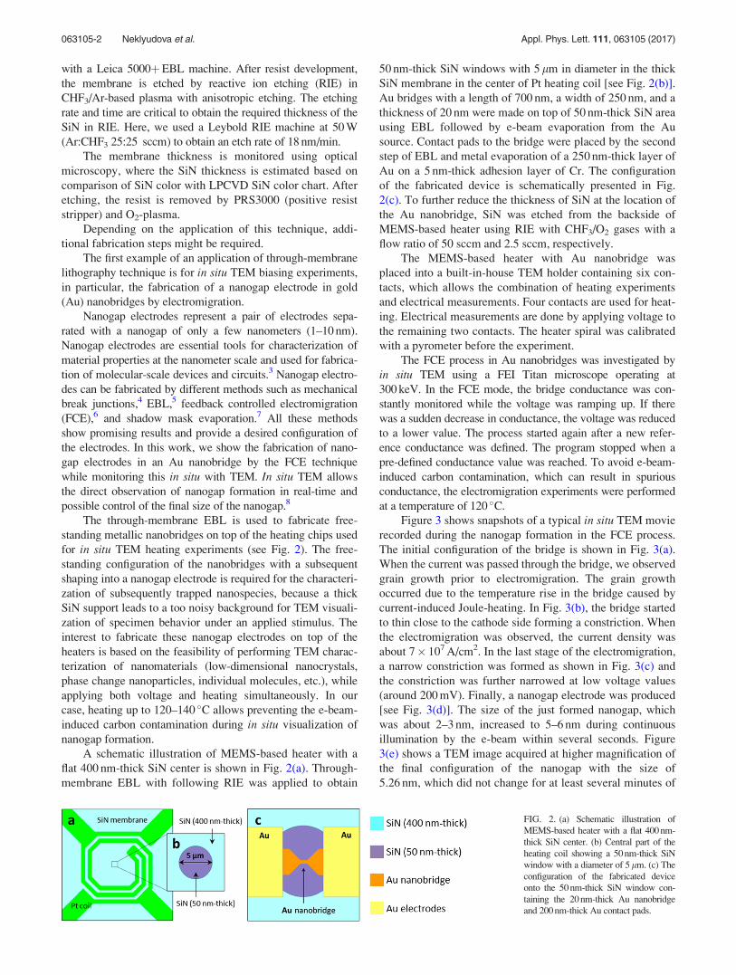
A schematic illustration of MEMS-based heater with a
flat 400 nm-thick SiN center is shown in Fig. 2(a). Through-
membrane EBL with following RIE was applied to obtain
50 nm-thick SiN windows with 5 lm in diameter in the thick
SiN membrane in the center of Pt heating coil [see Fig. 2(b)].
Au bridges with a length of 700 nm, a width of 250 nm, and a
thickness of 20 nm were made on top of 50 nm-thick SiN area
using EBL followed by e-beam evaporation from the Au
source. Contact pads to the bridge were placed by the second
step of EBL and metal evaporation of a 250 nm-thick layer of
Au on a 5 nm-thick adhesion layer of Cr. The configuration
of the fabricated device is schematically presented in Fig.
2(c). To further reduce the thickness of SiN at the location of
the Au nanobridge, SiN was etched from the backside of
MEMS-based heater using RIE with CHF3/O2 gases with a
flow ratio of 50 sccm and 2.5 sccm, respectively.
The MEMS-based heater with Au nanobridge was
placed into a built-in-house TEM holder containing six con-
tacts, which allows the combination of heating experiments
and electrical measurements. Four contacts are used for heat-
ing. Electrical measurements are done by applying voltage to
the remaining two contacts. The heater spiral was calibrated
with a pyrometer before the experiment.
The FCE process in Au nanobridges was investigated by
in situ TEM using a FEI Titan microscope operating at
300 keV. In the FCE mode, the bridge conductance was con-
stantly monitored while the voltage was ramping up. If there
was a sudden decrease in conductance, the voltage was reduced
to a lower value. The process started again after a new refer-
ence conductance was defined. The program stopped when a
pre-defined conductance value was reached. To avoid e-beam-
induced carbon contamination, which can result in spurious
conductance, the electromigration experiments were performed
at a temperature of 120 �C.
Figure 3 shows snapshots of a typical in situ TEM movie
recorded during the nanogap formation in the FCE process.
The initial configuration of the bridge is shown in Fig. 3(a).
When the current was passed through the bridge, we observed
grain growth prior to electromigration. The grain growth
occurred due to the temperature rise in the bridge caused by
current-induced Joule-heating. In Fig. 3(b), the bridge started
to thin close to the cathode side forming a constriction. When
the electromigration was observed, the current density was
about 7� 107 A/cm2. In the last stage of the electromigration,
a narrow constriction was formed as shown in Fig. 3(c) and
the constriction was further narrowed at low voltage values
(around 200 mV). Finally, a nanogap electrode was produced
[see Fig. 3(d)]. The size of the just formed nanogap, which
was about 2–3 nm, increased to 5–6 nm during continuous
illumination by the e-beam within several seconds. Figure
3(e) shows a TEM image acquired at higher magnification of
the final configuration of the nanogap with the size of
5.26 nm, which did not change for at least several minutes of
FIG. 2. (a) Schematic illustration of
MEMS-based heater with a flat 400 nm-
thick SiN center. (b) Central part of the
heating coil showing a 50 nm-thick SiN
window with a diameter of 5lm. (c) The
configuration of the fabricated device
onto the 50 nm-thick SiN window con-
taining the 20 nm-thick Au nanobridge
and 200 nm-thick Au contact pads.
063105-2 Neklyudova et al. Appl. Phys. Lett. 111, 063105 (2017)

e-beam irradiation. At the moment when the nanogap elec-
trode was initially formed, the tips of the electrodes were
sharp. However, after several seconds when the gap size
increased, the shape of the electrode tips became more smooth,
which is likely due to surface tension of Au. This observation
is in agreement with the previous reports of Zandbergen et al.9
on continued relaxation of Au nanogaps formed by e-beam
bombardment even after the intense irradiation is completed,
also with the report of Strachan et al.10 on the evolution of Au
nanogap electrodes. A typical I–V curve of the FCE process in
Au nanobridges is shown in Fig. 3(f).
In Fig. 3(d), one can see a thin layer of SiN remained
around the nanogap. Compared to standard fabrication meth-
ods of nanogaps on top of SiN membranes with the thick-
nesses of 100 nm,11 our technique allows the fabrication of
nanogap electrodes with a thin SiN layer beneath it.
To remove the SiN completely, we applied a vaporized
HF by SPTS etch vapor system, using a 190 sccm HF flow
that enabled to etch remained 2–3 nm SiN completely without
damaging the metal lines (see Fig. S2 in the supplementary
material). After applying HF treatment, we observed no SiN
near the metal structures.
The second example of application of through-
membrane lithography technique is for low-noise graphene
nanopore devices. Graphene nanopores represent a promising
tool for fast and direct sequencing of DNA molecules.19 In
nanopore sensing, a tiny hole (“nanopore”) in a membrane
that separates two compartments of electrolyte solution is the
only pathway for ions and molecules to pass. When a voltage
is applied over the membrane, an ionic current is induced
with a resistance that is set by the pore length and width, and
negatively charged DNA molecules will move towards the
positive pole. When a DNA molecule traverses through the
nanopore, it impedes the ionic current, which leads to a resis-
tive spike (typically �1 nA) in the ionic current baseline (sev-
eral nA). The two great advantages of graphene nanopores, to
the more commonly used SiN solid-state nanopores, are that
the graphene is atomically thin, which optimizes the sensing
resolution as the pore hosts a minimum number of bases at
the same time, and its conductive nature facilitates new
modes of base detection.
One downside of these graphene nanopore systems is
that the noise levels in the ionic current are relatively high
(about two orders of magnitude higher than in SiN pores12).
The noise in the graphene nanopore ionic current is charac-
terized by a 1/f dependence [Fig. 4(c), blue curve]. It has
been shown that increasing the number of graphene layers,13
the use of additional layers of other materials,13,14 or reduc-
ing the area of freestanding graphene can lower the noise
levels in the graphene nanopore currents.15 Reducing the
area of freestanding graphene (diameter �100 nm) provides
the most elegant approach to the noise reduction as the atom-
ically thin membrane is retained.
As in the heater chip layout described above, a Pt heater
is embedded in the supporting SiN membrane, which is used
to heat up the graphene during STEM sculpting of the gra-
phene nanopore,16,17 leading to a total membrane thickness of
600 nm [Fig. 4(a)]. The formation of a narrow (d�100 nm)
access channel in such a “thick” membrane would add a large
channel resistance to the circuit. This is an unwanted effect,
as in the ideal case the graphene nanopore exclusively sets the
resistance and thus behaves as the sensing probe. To reduce
the area of freestanding graphene diameter to �100 nm, while
preventing the addition of a huge channel resistance, the fabri-
cation of a thin window in the SiN membrane is needed.
Using the through-membrane EBL technique and RIE that is
described in this paper, 5� 5 lm2 windows of �50–150 nm
thickness were fabricated, after which pores with diameters of
�50–150 nm were made using focused ion beam drilling.
Graphene flakes were subsequently transferred onto these
chips,18 and finally �10 nm pores were sculpted in the gra-
phene using high-temperature sculpting with STEM.16,17
We measured and analyzed ionic current baselines of 24
thin window devices with reduced areas of freestanding gra-
phene (�50–150 nm in diameter) and compared their noise
levels to those of 45 devices with 600 nm-thick windows
FIG. 3. Snapshots taken from the insitu TEM movie recorded during the
FCE process in the Au nanobridge. (a)
The original bridge. (b) and (c) TEM
images showing formation of nanogaps
in the Au bridge during FCE. (d) TEM
image acquired after nanogap forma-
tion; arrows indicate the areas with a
thin SiN layer. (e) Enlarged area of (d)
showing Au electrodes separated with
a nanogap of 5.26 nm. (f) I-V curve of
the FCE process.
063105-3 Neklyudova et al. Appl. Phys. Lett. 111, 063105 (2017)
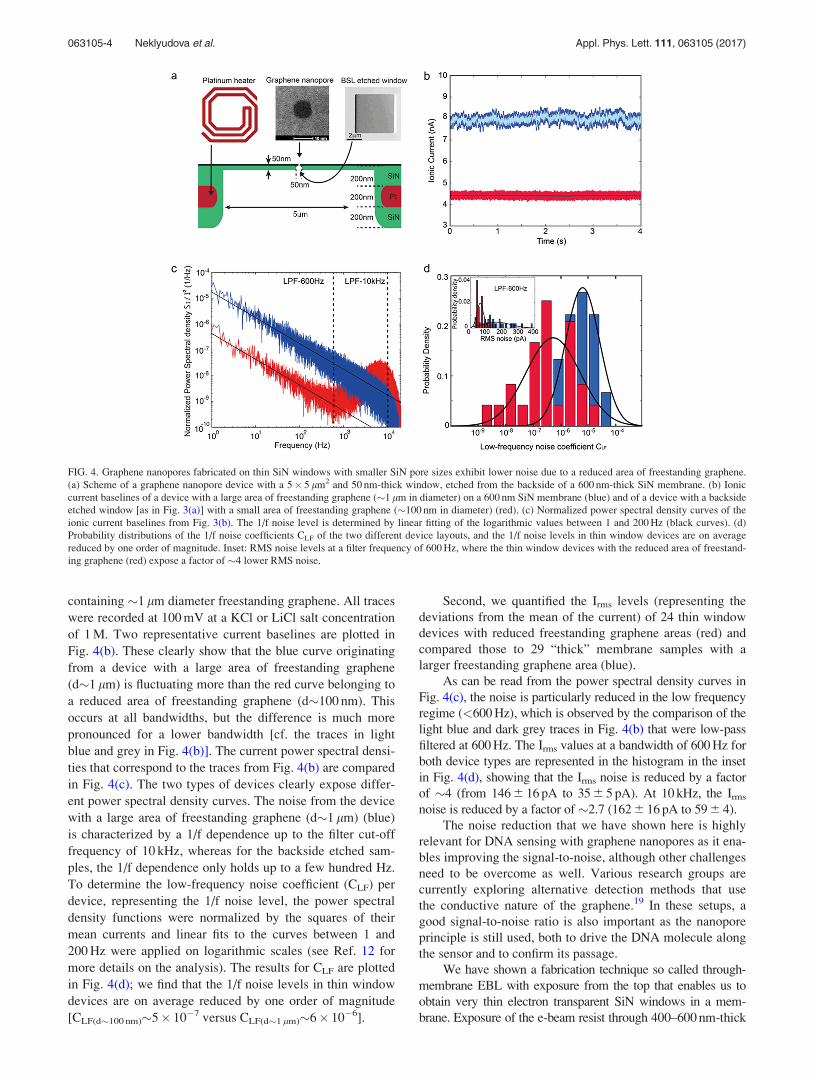
containing �1 lm diameter freestanding graphene. All traces
were recorded at 100 mV at a KCl or LiCl salt concentration
of 1 M. Two representative current baselines are plotted in
Fig. 4(b). These clearly show that the blue curve originating
from a device with a large area of freestanding graphene
(d�1 lm) is fluctuating more than the red curve belonging to
a reduced area of freestanding graphene (d�100 nm). This
occurs at all bandwidths, but the difference is much more
pronounced for a lower bandwidth [cf. the traces in light
blue and grey in Fig. 4(b)]. The current power spectral densi-
ties that correspond to the traces from Fig. 4(b) are compared
in Fig. 4(c). The two types of devices clearly expose differ-
ent power spectral density curves. The noise from the device
with a large area of freestanding graphene (d�1 lm) (blue)
is characterized by a 1/f dependence up to the filter cut-off
frequency of 10 kHz, whereas for the backside etched sam-
ples, the 1/f dependence only holds up to a few hundred Hz.
To determine the low-frequency noise coefficient (CLF) per
device, representing the 1/f noise level, the power spectral
density functions were normalized by the squares of their
mean currents and linear fits to the curves between 1 and
200 Hz were applied on logarithmic scales (see Ref. 12 for
more details on the analysis). The results for CLF are plotted
in Fig. 4(d); we find that the 1/f noise levels in thin window
devices are on average reduced by one order of magnitude
[CLF(d�100 nm)�5� 10�7 versus CLF(d�1 lm)�6� 10�6].
Second, we quantified the Irms levels (representing the
deviations from the mean of the current) of 24 thin window
devices with reduced freestanding graphene areas (red) and
compared those to 29 “thick” membrane samples with a
larger freestanding graphene area (blue).
As can be read from the power spectral density curves in
Fig. 4(c), the noise is particularly reduced in the low frequency
regime (<600 Hz), which is observed by the comparison of the
light blue and dark grey traces in Fig. 4(b) that were low-pass
filtered at 600 Hz. The Irms values at a bandwidth of 600 Hz for
both device types are represented in the histogram in the inset
in Fig. 4(d), showing that the Irms noise is reduced by a factor
of �4 (from 146 6 16 pA to 35 6 5 pA). At 10 kHz, the Irms
noise is reduced by a factor of �2.7 (162 6 16 pA to 59 6 4).
The noise reduction that we have shown here is highly
relevant for DNA sensing with graphene nanopores as it ena-
bles improving the signal-to-noise, although other challenges
need to be overcome as well. Various research groups are
currently exploring alternative detection methods that use
the conductive nature of the graphene.19 In these setups, a
good signal-to-noise ratio is also important as the nanopore
principle is still used, both to drive the DNA molecule along
the sensor and to confirm its passage.
We have shown a fabrication technique so called through-
membrane EBL with exposure from the top that enables us to
obtain very thin electron transparent SiN windows in a mem-
brane. Exposure of the e-beam resist through 400–600 nm-thick
FIG. 4. Graphene nanopores fabricated on thin SiN windows with smaller SiN pore sizes exhibit lower noise due to a reduced area of freestanding graphene.
(a) Scheme of a graphene nanopore device with a 5� 5 lm2 and 50 nm-thick window, etched from the backside of a 600 nm-thick SiN membrane. (b) Ionic
current baselines of a device with a large area of freestanding graphene (�1 lm in diameter) on a 600 nm SiN membrane (blue) and of a device with a backside
etched window [as in Fig. 3(a)] with a small area of freestanding graphene (�100 nm in diameter) (red). (c) Normalized power spectral density curves of the
ionic current baselines from Fig. 3(b). The 1/f noise level is determined by linear fitting of the logarithmic values between 1 and 200 Hz (black curves). (d)
Probability distributions of the 1/f noise coefficients CLF of the two different device layouts, and the 1/f noise levels in thin window devices are on average
reduced by one order of magnitude. Inset: RMS noise levels at a filter frequency of 600 Hz, where the thin window devices with the reduced area of freestand-
ing graphene (red) expose a factor of �4 lower RMS noise.
063105-4 Neklyudova et al. Appl. Phys. Lett. 111, 063105 (2017)

SiN membranes facilitates the manufacturing of a differnt
type of geometry in which one can control and maintain the
flatness of the topside of the membrane while creating very
thin windows at certain locations. Compared to optical lithog-
raphy, EBL allows one to obtain smaller structures with a
high accuracy down to the nanometer scale. The two applica-
tions of through-membrane EBL given in this paper are fron-
tier projects and examples of the potential of this fabrication
technique.
In nanogap formation, we have demonstrated that this
unique fabrication technique enables us to obtain a very
thin SiN layer. The application of additional etching steps
(with vaporized HF) allows the removal of the membrane
completely for further applications of nanogap electrodes.
In the second application, the thin windows are used to
fabricate low noise nanopores in graphene to improve the
signal-to-noise levels in DNA sensing experiments. This
development is beneficial for further graphene nanopore
measurements and for graphene-based DNA sequencing.
In addition to these demonstrated applications, having
an ultrathin SiN electron transparent window on the top of
the membrane will have advantages on in situ TEM liquid
cell, nanoreactor, and battery studies since it offers a flat
surface on the top that enables smooth liquid flow for liquid
cell studies and controllable lift off materials after
deposition.
See supplementary material for Figs. S1 and S2. Figure
S1 shows a schematic illustration of the chip for in situ TEM
heating experiments. Figure S2 shows the metallic structure
with a thin SiN layer after plasma etching and without SiN
after vaporized HF treatment.
The authors gratefully acknowledge ERC Project
NEMinTEM 267922, the STW Perspectief project UPON
and European Union’s Horizon 2020 research and
innovation programme under Grant Agreement No. 696656.
1M. A. van Huis, N. P. Young, G. Pandraud, J. F. Creemer, D.
Vanmaekelbergh, A. I. Kirkland, and H. W. Zandbergen, Adv. Mater. 21,
4992 (2009).2M. Neklyudova, C. Sabater, A. K. Erdamar, J. M. van Ruitenbeek, and H.
W. Zandbergen, Appl. Phys. Lett. 110, 103101 (2017).3T. Li, W. Hu, and D. Zhu, Adv. Mater. 22, 286 (2010).4M. A. Reed, C. Zhou, C. J. Muller, T. P. Burgin, and J. M. Tour, Science
278, 252 (1997).5W. Chen, H. Ahmed, and K. Nakazoto, Appl. Phys. Lett. 66, 3383 (1995).6J. Park, A. N. Pasupathy, J. I. Goldsmith, C. Chang, Y. Yaish, J. R. Petta,
M. Rinkoski, J. P. Sethna, H. D. Abru~na, P. L. McEuen, and D. C. Ralph,
Nature 417, 722 (2002).7S. Kubatkin, A. Danilov, M. Hjort, J. Cornil, J.-L. Br�edas, N. Stuhr-
Hansen, P. Hedegard, and T. Bjørnholm, Nature 425, 698 (2003).8M. Rudeneva, B. Gao, F. Prins, Q. Xu, H. S. J. van der Zant, and H. W.
Zandbergen, Microsc. Microanal. 19, 43 (2013).9H. W. Zandbergen, R. J. H. A. van Duuren, P. F. A. Alkemade, G.
Lientschnig, O. Vasquez, C. Dekker, and F. D. Tichelaar, Nano Lett. 5,
549 (2005).10D. R. Strachan, D. E. Smith, M. D. Fischbein, D. E. Johnston, B. S. Guiton,
M. Drndic, D. A. Bonnell, and A. T. Johnson, Nano Lett. 6, 441 (2006).11M. Neklyudova, “Casimir PhD-series, Delft-Leiden 2016-14.” Ph.D. thesis
(Technische Universiteit Delft, 2016), Chap. 6.12S. J. Heerema, G. F. Schneider, M. Rozemuller, L. Vicarelli, H. W.
Zandbergen, and C. Dekker, Nanotechnology 26, 074001 (2015).13C. A. Merchant, K. Healy, M. Wanunu, V. Ray, N. Peterman, J. Bartel, M.
D. Fischbein, K. Venta, Z. Luo, A. T. Charlie Johnson, and M. Drndic,
Nano Lett. 10, 2915 (2010).14B. Venkatesan, D. Estrada, S. Banerjee, X. Jin, V. E. Dorgan, M.-H. Bae,
N. R. Aluru, E. Pop, and R. Bashir, ACS Nano 6, 441 (2012).15S. Garaja, S. Liua, J. A. Golovchenko, and D. Brantonc, Proc. Nat. Acad.
Sci. U. S. A. 110, 12192 (2013).16B. Song, G. F. Schneider, Q. Xu, G. Pandraud, C. Dekker, and H. W.
Zandbergen, Nano Lett. 11, 2247 (2011).17Q. Xu, M.-Y. Wu, G. F. Schneider, L. Houben, S. K. Malladi, C. Dekker,
E. Yucelen, R. E. Dunin-Borkowski, and H. W. Zandbergen, ACS Nano 7,
1566 (2013).18G. F. Schneider, V. E. Calado, H. W. Zandbergen, L. M. K. Vandersypen,
and C. Dekker, Nano Lett. 10, 1912 (2010).19S. J. Heerema and C. Dekker, Nat. Nanotechnol. 11, 127 (2016).
063105-5 Neklyudova et al. Appl. Phys. Lett. 111, 063105 (2017)