ltc3616 - 6a, 4mhz monolithic synchronous step-down dc/dc ...€¦ · 6a, 4mhz monolithic...
TRANSCRIPT

LTC3616
13616fc
For more information www.linear.com/LTC3616
Typical applicaTion
FeaTures
applicaTions
DescripTion
6A, 4MHz Monolithic Synchronous Step-Down
DC/DC Converter
The LTC®3616 is a low quiescent current monolithic syn-chronous buck regulator using a current mode, constant frequency architecture. The no-load DC supply current in sleep mode is only 70µA while maintaining the output voltage (Burst Mode operation) at no load, dropping to zero current in shutdown. The 2.25V to 5.5V input supply voltage range makes the LTC3616 ideally suited for single Li-Ion as well as fixed low voltage input applications. 100% duty cycle capability provides low dropout operation, extending the operating time in battery-powered systems.
The operating frequency is externally programmable up to 4MHz, allowing the use of small surface mount inductors. For switching noise-sensitive applications, the LTC3616 can be synchronized to an external clock at up to 4MHz.
Forced continuous mode operation in the LTC3616 reduces noise and RF interference. Adjustable compensation allows the transient response to be optimized over a wide range of loads and output capacitors.
The internal synchronous switch increases efficiency and eliminates the need for an external catch diode, saving external components and board space. The LTC3616 is offered in a leadless 24-pin 3mm × 5mm thermally enhanced QFN package.L, LT, LTC, LTM, Linear Technology, the Linear logo and Burst Mode are registered trademarks of Linear Technology Corporation. All other trademarks are the property of their respective owners. Protected by U.S. Patents, including 6580258, 5481178, 5994885, 6304066, 6498466, 6611131.
Efficiency and Power Lossvs Load Current
n 6A Output Currentn 2.25V to 5.5V Input Voltage Rangen Low Output Ripple Burst Mode® Operation: IQ = 75µAn ±1% Output Voltage Accuracyn Output Voltage Down to 0.6Vn High Efficiency: Up to 95%n Low Dropout Operation: 100% Duty Cyclen Programmable Slew Rate on SW Node Reduces
Noise and EMIn Adjustable Switching Frequency: Up to 4MHzn Optional Active Voltage Positioning (AVP) with
Internal Compensationn Selectable Pulse-Skipping/Forced Continuous/Burst
Mode Operation with Adjustable Burst Clampn Programmable Soft-Startn Inputs for Start-Up Tracking or External Referencen DDR Memory Mode, IOUT = ±3A n Available in a 24-Pin 3mm × 5mm QFN
Thermally Enhanced Package
n Point-of-Load Suppliesn Distributed Power Suppliesn Portable Computer Systemsn DDR Memory Terminationn Handheld Devices
OUTPUT CURRENT (mA)
30
EFFI
CIEN
CY (%
)
POWER LOSS (W
)
90
100
20
10
80
50
70
60
40
1 100 1000 10000
3616 TA01b
0
0
1
0.1
0.01
10
VIN = 2.8VVIN = 3.3VVIN = 5VVOUT = 2.5V
RUNTRACK/SSRT/SYNC
PGOODITH
SGNDPGND
VIN2.7V TO 5.5V
SRLIM/DDR
SVIN
LTC3616 SW
PVIN
220nH
665k
210k
3616 TA01a
22µF×4
MODE VFB
47µF×2
VOUT2.5V6A

LTC3616
23616fc
For more information www.linear.com/LTC3616
absoluTe MaxiMuM raTings
PVIN, SVIN Voltages ..................................... –0.3V to 6VSW Voltage ................................. –0.3V to (PVIN + 0.3V)ITH, RT/SYNC Voltages ............... –0.3V to (SVIN + 0.3V)SRLIM, TRACK/SS Voltages ....... –0.3V to (SVIN + 0.3V)MODE, RUN, VFB Voltages .......... –0.3V to (SVIN + 0.3V)PGOOD Voltage ............................................ –0.3V to 6VOperating Junction Temperature Range (Notes 2, 11) .......................................... –55°C to 150°CStorage Temperature.............................. –65°C to 150°CReflow Peak Body Temperature (QFN) .................. 260°C
(Note 1)TOP VIEW
25
UDD PACKAGE24-LEAD (3mm × 5mm) PLASTIC QFN
SRLIM/DDR
RT/SYNC
SGND
PVIN
SW
SW
SW
SW
PGOOD
RUN
SVIN
PVIN
SW
SW
SW
SW
NC
PVIN
PVIN NC
TRAC
K/SS
ITH
V FB
MOD
E
6
5
4
3
2
1
7
8
15
16
17
18
19
20
14
13
9 10 11 12
24 23 22 21
TJMAX = 150°C, θJA = 38°C/W
EXPOSED PAD (PIN 25) IS PGND, MUST BE SOLDERED TO PCB
pin conFiguraTion
orDer inForMaTionLEAD FREE FINISH TAPE AND REEL PART MARKING* PACKAGE DESCRIPTION TEMPERATURE RANGE
LTC3616EUDD#PBF LTC3616EUDD#TRPBF LDYG 24-Lead (3mm × 5mm) Plastic QFN –40°C to 125°C
LTC3616IUDD#PBF LTC3616IUDD#TRPBF LDYG 24-Lead (3mm × 5mm) Plastic QFN –40°C to 125°C
LTC3616HUDD#PBF LTC3616HUDD#TRPBF LDYG 24-Lead (3mm × 5mm) Plastic QFN –40°C to 150°C
LTC3616MPUDD#PBF LTC3616MPUDD#TRPBF LDYG 24-Lead (3mm × 5mm) Plastic QFN –55°C to 150°C
Consult LTC Marketing for parts specified with wider operating temperature ranges. *The temperature grade is identified by a label on the shipping container.Consult LTC Marketing for information on non-standard lead based finish parts.For more information on lead free part marking, go to: http://www.linear.com/leadfree/ For more information on tape and reel specifications, go to: http://www.linear.com/tapeandreel/
LTC3616
33616fc
For more information www.linear.com/LTC3616
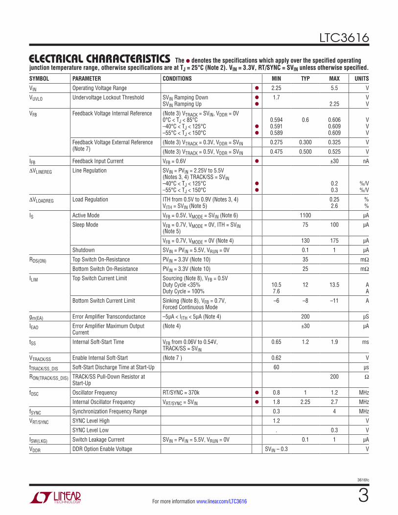
elecTrical characTerisTics The l denotes the specifications which apply over the specified operating junction temperature range, otherwise specifications are at TJ = 25°C (Note 2). VIN = 3.3V, RT/SYNC = SVIN unless otherwise specified.
SYMBOL PARAMETER CONDITIONS MIN TYP MAX UNITS
VIN Operating Voltage Range l 2.25 5.5 V
VUVLO Undervoltage Lockout Threshold SVIN Ramping Down SVIN Ramping Up
l
l
1.7 2.25
V V
VFB Feedback Voltage Internal Reference (Note 3) VTRACK = SVIN, VDDR = 0V 0°C < TJ < 85°C –40°C < TJ < 125°C –55°C < TJ < 150°C
l
l
0.594 0.591 0.589
0.6
0.606 0.609 0.609
V V V
Feedback Voltage External Reference (Note 7)
(Note 3) VTRACK = 0.3V, VDDR = SVIN 0.275 0.300 0.325 V
(Note 3) VTRACK = 0.5V, VDDR = SVIN 0.475 0.500 0.525 V
IFB Feedback Input Current VFB = 0.6V l ±30 nA
∆VLINEREG Line Regulation SVIN = PVIN = 2.25V to 5.5V (Notes 3, 4) TRACK/SS = SVIN –40°C < TJ < 125°C –55°C < TJ < 150°C
l
l
0.2 0.3
%/V %/V
∆VLOADREG Load Regulation ITH from 0.5V to 0.9V (Notes 3, 4) VITH = SVIN (Note 5)
0.25 2.6
% %
IS Active Mode VFB = 0.5V, VMODE = SVIN (Note 6) 1100 µA
Sleep Mode VFB = 0.7V, VMODE = 0V, ITH = SVIN (Note 5)
75 100 µA
VFB = 0.7V, VMODE = 0V (Note 4) 130 175 µA
Shutdown SVIN = PVIN = 5.5V, VRUN = 0V 0.1 1 µA
RDS(ON) Top Switch On-Resistance PVIN = 3.3V (Note 10) 35 mΩ
Bottom Switch On-Resistance PVIN = 3.3V (Note 10) 25 mΩ
ILIM Top Switch Current Limit Sourcing (Note 8), VFB = 0.5V Duty Cycle <35% Duty Cycle = 100%
10.5 7.6
12
13.5
A A
Bottom Switch Current Limit Sinking (Note 8), VFB = 0.7V, Forced Continuous Mode
–6 –8 –11 A
gm(EA) Error Amplifier Transconductance –5µA < IITH < 5µA (Note 4) 200 µS
IEAO Error Amplifier Maximum Output Current
(Note 4) ±30 µA
tSS Internal Soft-Start Time VFB from 0.06V to 0.54V, TRACK/SS = SVIN
0.65 1.2 1.9 ms
VTRACK/SS Enable Internal Soft-Start (Note 7 ) 0.62 V
tTRACK/SS_DIS Soft-Start Discharge Time at Start-Up 60 µs
RON(TRACK/SS_DIS) TRACK/SS Pull-Down Resistor at Start-Up
200 Ω
fOSC Oscillator Frequency RT/SYNC = 370k l 0.8 1 1.2 MHz
Internal Oscillator Frequency VRT/SYNC = SVIN l 1.8 2.25 2.7 MHz
fSYNC Synchronization Frequency Range 0.3 4 MHz
VRT/SYNC SYNC Level High 1.2 V
SYNC Level Low . 0.3 V
ISW(LKG) Switch Leakage Current SVIN = PVIN = 5.5V, VRUN = 0V 0.1 1 µA
VDDR DDR Option Enable Voltage SVIN – 0.3 V
LTC3616
43616fc
For more information www.linear.com/LTC3616
Note 1: Stresses beyond those listed under Absolute Maximum Ratings may cause permanent damage to the device. Exposure to any Absolute Maximum Rating condition for extended periods may affect device reliability and lifetime.Note 2: The LTC3616 is tested under pulsed load conditions such that TJ ≈ TA. The LTC3616E is guaranteed to meet specifications from 0°C to 85°C junction temperature. Specifications over the –40°C to 125°C operating junction temperature range are assured by design, characterization and correlation with statistical process controls. The LTC3616I is guaranteed to meet specifications over the –40°C to 125°C operating junction temperature, the LTC3616H is guaranteed to meet specifications over the –40°C to 150°C operating junction temperature range and the LTC36146MP is guaranteed and tested to meet specifications over the full –55°C to 150°C operating junction temperature range. High junction temperatures degrade operating lifetimes; operating lifetime is derated for temperature greater than 125°C. Note that the maximum ambient temperature consistent with these specifications is determined by specific operating conditions in conjunction with board layout, the rated package thermal impedance and other environmental factors. The junction temperature (TJ) is calculated from the ambient temperature (TA) and power dissipation (PD) according to the formula: TJ = TA + (PD • θJA°C/W), where θJA is the package thermal impedance. The maximum ambient temperature is determined by specific operating conditions in conjunction with board layout, the rated package thermal resistance and other environmental factors.
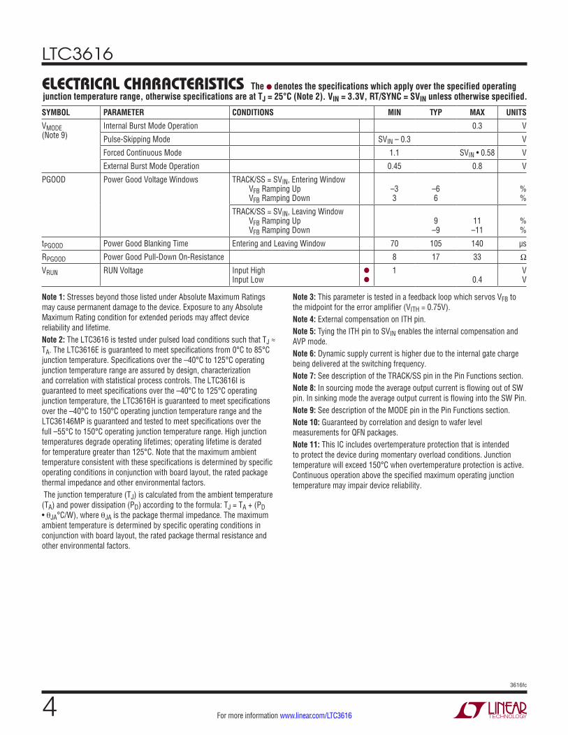
elecTrical characTerisTics The l denotes the specifications which apply over the specified operating junction temperature range, otherwise specifications are at TJ = 25°C (Note 2). VIN = 3.3V, RT/SYNC = SVIN unless otherwise specified.
SYMBOL PARAMETER CONDITIONS MIN TYP MAX UNITS
VMODE (Note 9)
Internal Burst Mode Operation 0.3 V
Pulse-Skipping Mode SVIN – 0.3 V
Forced Continuous Mode 1.1 SVIN • 0.58 V
External Burst Mode Operation 0.45 0.8 V
PGOOD Power Good Voltage Windows TRACK/SS = SVIN, Entering Window VFB Ramping Up VFB Ramping Down
–3 3
–6 6
% %
TRACK/SS = SVIN, Leaving Window VFB Ramping Up VFB Ramping Down
9
–9
11
–11
% %
tPGOOD Power Good Blanking Time Entering and Leaving Window 70 105 140 µs
RPGOOD Power Good Pull-Down On-Resistance 8 17 33 Ω
VRUN RUN Voltage Input High Input Low
l
l
1 0.4
V V
Note 3: This parameter is tested in a feedback loop which servos VFB to the midpoint for the error amplifier (VITH = 0.75V). Note 4: External compensation on ITH pin.Note 5: Tying the ITH pin to SVIN enables the internal compensation and AVP mode.Note 6: Dynamic supply current is higher due to the internal gate charge being delivered at the switching frequency.Note 7: See description of the TRACK/SS pin in the Pin Functions section.Note 8: In sourcing mode the average output current is flowing out of SW pin. In sinking mode the average output current is flowing into the SW Pin.Note 9: See description of the MODE pin in the Pin Functions section.Note 10: Guaranteed by correlation and design to wafer level measurements for QFN packages.Note 11: This IC includes overtemperature protection that is intended to protect the device during momentary overload conditions. Junction temperature will exceed 150°C when overtemperature protection is active. Continuous operation above the specified maximum operating junction temperature may impair device reliability.

LTC3616
53616fc
For more information www.linear.com/LTC3616
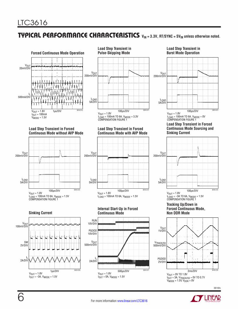
Typical perForMance characTerisTics
Efficiency vs Input Voltage Burst Mode Operation (VMODE = 0V)
Efficiency vs Frequency Burst Mode Operation (VMODE = 0V), IOUT = 2A
Line Regulation Burst Mode Operation Pulse-Skipping Mode Operation
INPUT VOLTAGE (V)
30
EFFI
CIEN
CY (%
)
40
50
60
70
100
90
2.5 3 43.5 4.5
3616 G04
5 5.5
80
VOUT = 1.8V
IOUT = 6mAIOUT = 600mAIOUT = 2AIOUT = 6A
INPUT VOLTAGE (V)2.20
–0.3
V OUT
ERR
OR (%
)
–0.2
–0.1
0
0.1
0.3
2.75 3.30 3.85 4.40
3616 G07
4.95 5.50
0.2
VOUT20mV/DIV
IL1A/DIV
20µs/DIV 3616 G08VOUT = 1.8VIOUT = 150mAVMODE = 0V
VOUT20mV/DIV
IL1A/DIV
20µs/DIV 3616 G09VOUT = 1.8VIOUT = 150mAVMODE = 3.3V
VIN = 3.3V, RT/SYNC = SVIN unless otherwise noted.
Efficiency vs Load Current Burst Mode Operation (VMODE = 0V)
Efficiency vs Load Current Burst Mode Operation (VMODE = 0V) Efficiency vs Load Current
Load Regulation (VIN = 3.3V, VOUT = 1.8V)
OUTPUT CURRENT (mA)0
–0.3
V OUT
ERR
OR (%
)
1.5
0.3
0.7
1.1
1.3
0.9
0.1
0.5
1000 2000 3000 4000
3616 G06
5000 6000
–0.1
FORCED CONTINUOUS MODEPULSE-SKIPPING MODEINTERNAL Burst Mode OPERATION
OUTPUT CURRENT (mA)
30
EFFI
CIEN
CY (%
)
90
100
20
10
80
50
70
60
40
1 100 1000 10000
3616 G01
010
VIN = 2.5VVIN = 3.3VVIN = 5V
VOUT = 1.8V
OUTPUT CURRENT (mA)
30EF
FICI
ENCY
(%)
90
100
20
10
80
50
70
60
40
1 100 1000 10000
3616 G02
010
VIN = 2.5VVIN = 3.3VVIN = 5V
VOUT = 1.2V
OUTPUT CURRENT (mA)
30
EFFI
CIEN
CY (%
)
90
100
20
10
80
50
70
60
40
1 100 1000 10000
3616 G03
010
Burst Mode OPERATIONPULSE-SKIPPINGFORCED CONTINUOUS
VOUT = 1.8V, VIN = 3.3V
FREQUENCY (MHz)0.5
82
EFFI
CIEN
CY (%
)
858483
8687888990
9594
1 1.5 2.52 3 3.5
3616 G05
4 4.5
939291
VIN = 3.3VVOUT = 1.8V
150nH330nH470nH
LTC3616
63616fc
For more information www.linear.com/LTC3616
Sinking CurrentInternal Start-Up in Forced Continuous Mode
Tracking Up/Down in Forced Continuous Mode, Non DDR Mode
Load Step Transient in Forced Continuous Mode without AVP Mode
Load Step Transient in Forced Continuous Mode with AVP Mode
Load Step Transient in Forced Continuous Mode Sourcing and Sinking Current
VOUT1V/DIV
VTRACK/SS500mV/DIV
PGOOD2V/DIV
2ms/DIV 3616 G18
VOUT = 0V TO 1.8VIOUT = 3A, VTRACK/SS = 0V TO 0.7VVMODE = 1.5V, VDDR = 0V
Typical perForMance characTerisTics VIN = 3.3V, RT/SYNC = SVIN unless otherwise noted.
VOUT200mV/DIV
ILOAD5A/DIV
100µs/DIV 3616 G13
VOUT = 1.8VILOAD = 100mA TO 6A, VMODE = 1.5VCOMPENSATION FIGURE 1
VOUT200mV/DIV
ILOAD5A/DIV
100µs/DIV 3616 G14
VOUT = 1.8VILOAD = 100mA TO 6A, VMODE = 1.5V
VOUT200mV/DIV
ILOAD5A/DIV
100µs/DIV 3616 G15
VOUT = 1.8VILOAD = –3A TO 6A, VMODE = 1.5VCOMPENSATION FIGURE 1
VOUT100mV/DIV
SW2V/DIV
IL2A/DIV
1µs/DIV 3616 G16
VOUT = 1.8VIOUT = –3A, VMODE = 1.5V
IL2A/DIV
VOUT500mV/DIV
PGOOD10V/DIV
RUN10V/DIV
500µs/DIV 3616 G17
VOUT = 1.8VIOUT = 0A, VMODE = 1.5V
Forced Continuous Mode Operation
VOUT20mV/DIV
IL500mA/DIV
1µs/DIV 3616 G10VOUT = 1.8VIOUT = 100mAVMODE = 1.5V
Load Step Transient in Pulse-Skipping Mode
Load Step Transient in Burst Mode Operation
VOUT200mV/DIV
ILOAD5A/DIV
100µs/DIV 3616 G11
VOUT = 1.8VILOAD = 100mA TO 6A, VMODE = 3.3VCOMPENSATION FIGURE 1
VOUT200mV/DIV
ILOAD5A/DIV
100µs/DIV 3616 G12
VOUT = 1.8VILOAD = 100mA TO 6A, VMODE = 0VCOMPENSATION FIGURE 1
LTC3616
73616fc
For more information www.linear.com/LTC3616
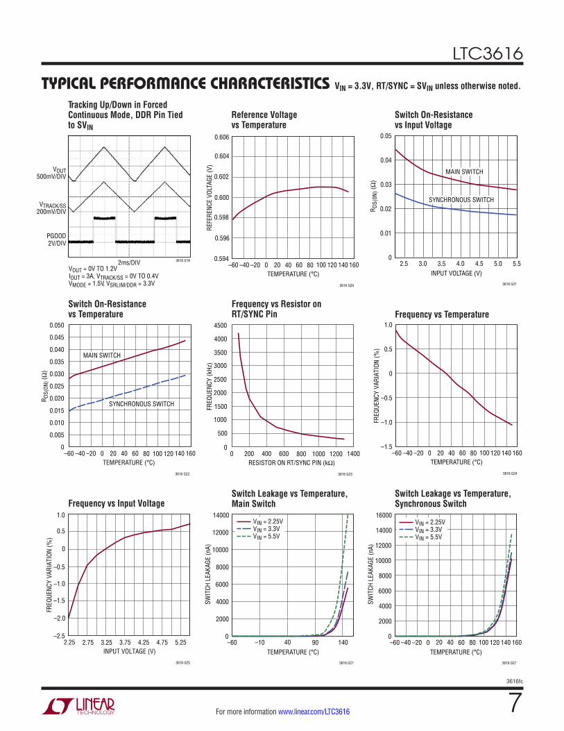
Tracking Up/Down in Forced Continuous Mode, DDR Pin Tied to SVIN
Reference Voltage vs Temperature
Switch On-Resistance vs Input Voltage
Frequency vs Input VoltageSwitch Leakage vs Temperature, Main Switch
Switch Leakage vs Temperature, Synchronous Switch
Switch On-Resistance vs Temperature
Frequency vs Resistor on RT/SYNC Pin Frequency vs Temperature
TEMPERATURE (°C)–60 –40
0.594
REFE
RENC
E VO
LTAG
E (V
)
0.596
0.600
0.602
0.604
0 40 60 160140
3616 G20
0.598
–20 20 80 100 120
0.606
INPUT VOLTAGE (V)2.5
R DS(
0N) (
Ω)
0.05
4.5
3616 G21
0.04
0.02
0.03
0.01
03.0 3.5 4.0 5.0 5.5
MAIN SWITCH
SYNCHRONOUS SWITCH
RESISTOR ON RT/SYNC PIN (kΩ)0
0
FREQ
UENC
Y (k
Hz)
500
1500
2000
2500
800
4500
3616 G23
1000
400200 1000 1200600 1400
3000
3500
4000
TEMPERATURE (°C)–60 –40
–1.5
FREQ
UENC
Y VA
RIAT
ION
(%)
–1.0
1.0
0 40 60 160140
3616 G24
–0.5
0.5
0
–20 20 80 100 120
INPUT VOLTAGE (V)2.25
–2.5
FREQ
UENC
Y VA
RIAT
ION
(%)
–2.0
–1.0
–0.5
0
1.0
3616 G25
–1.5
0.5
3.753.25 5.252.75 4.25 4.75
Typical perForMance characTerisTics VIN = 3.3V, RT/SYNC = SVIN unless otherwise noted.
TEMPERATURE (°C)–60 –40
0
R DS(
ON) (
Ω)
0.005
0.015
0.020
0.025
80
0.050
0.045
3616 G22
0.010
200 12060–20 10040 160140
0.030
0.035
0.040
SYNCHRONOUS SWITCH
MAIN SWITCH
TEMPERATURE (°C)–60
SWIT
CH L
EAKA
GE (n
A)
8000
10000
12000
140
3616 G27
6000
4000
090–10 40
2000
14000VIN = 2.25VVIN = 3.3VVIN = 5.5V
TEMPERATURE (°C)–60
SWIT
CH L
EAKA
GE (n
A)
8000
10000
12000
100
3616 G27
6000
4000
0–20 20 60–40 1600 40 80 140120
2000
16000
14000VIN = 2.25VVIN = 3.3VVIN = 5.5V
VOUT500mV/DIV
VTRACK/SS200mV/DIV
PGOOD2V/DIV
2ms/DIV 3616 G19
VOUT = 0V TO 1.2VIOUT = 3A, VTRACK/SS = 0V TO 0.4VVMODE = 1.5V, VSRLIM/DDR = 3.3V
LTC3616
83616fc
For more information www.linear.com/LTC3616
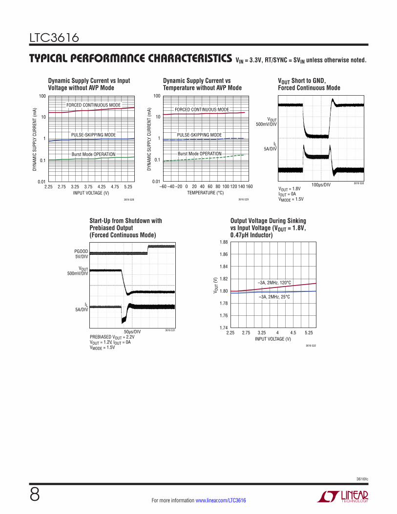
Start-Up from Shutdown with Prebiased Output (Forced Continuous Mode)
Output Voltage During Sinking vs Input Voltage (VOUT = 1.8V, 0.47µH Inductor)
Typical perForMance characTerisTics VIN = 3.3V, RT/SYNC = SVIN unless otherwise noted.
VOUT500mV/DIV
PGOOD5V/DIV
IL5A/DIV
50µs/DIV 3616 G31
PREBIASED VOUT = 2.2VVOUT = 1.2V, IOUT = 0AVMODE = 1.5V
INPUT VOLTAGE (V)
V OUT
(V)
1.86
1.84
1.82
1.80
1.78
1.88
2.25 41.74
1.76
3.252.75 4.5 5.25
3616 G32
–3A, 2MHz, 120°C
–3A, 2MHz, 25°C
Dynamic Supply Current vs Input Voltage without AVP Mode
VOUT Short to GND, Forced Continuous Mode
Dynamic Supply Current vs Temperature without AVP Mode
INPUT VOLTAGE (V)
0.1
DYNA
MIC
SUP
PLY
CURR
ENT
(mA)
1
10
100
2.25 3.25 3.75 4.25 4.750.01
2.75 5.25
3616 G28
FORCED CONTINUOUS MODE
PULSE-SKIPPING MODE
Burst Mode OPERATION
TEMPERATURE (°C)
0.1
DYNA
MIC
SUP
PLY
CURR
ENT
(mA)
1
10
100
–60 –40 40 80 120 1601400.01
0 20 60 100–20
3616 G29
FORCED CONTINUOUS MODE
PULSE-SKIPPING MODE
Burst Mode OPERATION
VOUT500mV/DIV
IL5A/DIV
100µs/DIV 3616 G30
VOUT = 1.8VIOUT = 0AVMODE = 1.5V

LTC3616
93616fc
For more information www.linear.com/LTC3616
pin FuncTionsSRLIM/DDR (Pin 1): Slew Rate Limit. Tying this pin to ground selects maximum slew rate. Minimum slew rate is selected when the pin is open. Connecting a resistor from SRLIM/DDR to ground allows the slew rate to be continuously adjusted. If SRLIM/DDR is tied to SVIN, DDR mode is selected. In DDR mode the slew rate limit is set to maximum.
RT/SYNC (Pin 2): Oscillator Frequency. This pin provides three ways of setting the constant switching frequency:
1. Connecting a resistor from RT/SYNC to ground will set the switching frequency based on the resistor value.
2. Driving the RT/SYNC pin with an external clock signal will synchronize the LTC3616 to the applied frequency. The slope compensation is automatically adapted to the external clock frequency.
3. Tying the RT/SYNC pin to SVIN enables the internal 2.25MHz oscillator frequency.
SGND (Pin 3): Signal Ground. All small-signal and com-pensation components should connect to this ground, which in turn should connect to PGND at a single point.
PVIN (Pins 4, 10, 11, 17): Power Input Supply. PVIN connects to the source of the internal P-channel power MOSFET. This pin is independent of SVIN and may be con-nected to the same voltage or to a lower voltage supply.
SW (Pins 5, 6, 7, 8, 13, 14, 15, 16): Switch Node. Con-nection to the inductor. These pins connect to the drains of the internal synchronous power MOSFET switches.
NC (Pins 9, 12): Can be connected to ground or left open.
SVIN (Pin 18): Signal Input Supply. This pin powers the internal control circuitry and is monitored by the under-voltage lockout comparator.
RUN (Pin 19): Enable Pin. Forcing this pin to ground shuts down the LTC3616. In shutdown, all functions are disabled and the chip draws <1µA of supply current.
PGOOD (Pin 20): Power Good. This open-drain output is pulled down to SGND on start-up and while the FB voltage is outside the power good voltage window. If the FB volt-age increases and stays inside the power good window for more than 100µs the PGOOD pin is released. If the
FB voltage leaves the power good window for more than 100µs the PGOOD pin is pulled down.
In DDR mode (DDR = VIN), the power good window moves in relation to the actual TRACK/SS pin voltage. During up/down tracking the PGOOD pin is always pulled down.
In shutdown the PGOOD output will actively pull down and may be used to discharge the output capacitors via an external resistor.
MODE (Pin 21): Mode Selection. Tying the MODE pin to SVIN or SGND enables pulse-skipping mode or Burst Mode operation (with an internal Burst Mode clamp), respectively. If this pin is held at slightly higher than half of SVIN, forced continuous mode is selected. Connecting this pin to an external voltage selects Burst Mode opera-tion with the burst clamp set to the pin voltage. See the Operation section for more details.
VFB (Pin 22): Voltage Feedback Input Pin. Senses the feedback voltage from the external resistive divider across the output.
ITH (Pin 23): Error Amplifier Compensation. The current comparator’s threshold increases with this control volt-age. Tying this pin to SVIN enables internal compensation and AVP mode.
TRACK/SS (Pin 24): Track/External Soft-Start/External Reference. Start-up behavior is programmable with the TRACK/SS pin:
1. Tying this pin to SVIN selects the internal soft-start circuit.
2. External soft-start timing can be programmed with a capacitor to ground and a resistor to SVIN.
3. TRACK/SS can be used to force the LTC3616 to track the start-up behavior of another supply.
The pin can also be used as external reference input. See the Applications Information section for more information.
PGND (Exposed Pad Pin 25): Power Ground. This pin connects to the source of the internal N-channel power MOSFET. This pin should be connected close to the (–) terminal of CIN and COUT.

LTC3616
103616fc
For more information www.linear.com/LTC3616
FuncTional block DiagraM
–
+
–
+
–
+
–
+
–
+
–
+
MODE
+
SLEEP
MODE
BURSTCOMPARATOR
ITH SENSECOMPARATOR
ERRORAMPLIFIER
FOLDBACKAMPLIFIER
0.6V
0.3V
R
0.555V
TRACK/SS
0.645V
SRLIM/DDR
EXPOSED PAD
3616 BD
SOFT-START
BANDGAPANDBIAS
–
+
–
+
VFB
RUN
SGND RT/SYNC ITH
SVIN – 0.3V
PVIN PVINSVIN
PGOOD
LOGIC
SW
SW
SW
SW
PGND
REVERSECOMPARATOR
IREV
OSCILLATOR
–
+INTERNAL
COMPENSATIONCURRENT
SENSE
SLOPECOMPENSATION
PMOS CURRENTCOMPARATORITH
LIMIT
PVIN PVIN
DRIVER
SW
SW
SW
SW

LTC3616
113616fc
For more information www.linear.com/LTC3616
Mode Selection
The MODE pin is used to select one of four different operating modes:
operaTionMain Control Loop
The LTC3616 is a monolithic, constant frequency, current mode step-down DC/DC converter. During normal opera-tion, the internal top power switch (P-channel MOSFET) is turned on at the beginning of each clock cycle. Current in the inductor increases until the current comparator trips and turns off the top power switch. The peak inductor cur-rent at which the current comparator trips is controlled by the voltage on the ITH pin. The error amplifier adjusts the voltage on the ITH pin by comparing the feedback signal from a resistor divider on the VFB pin with an internal 0.6V reference. When the load current increases, it causes a reduction in the feedback voltage relative to the reference. The error amplifier raises the ITH voltage until the average inductor current matches the new load current. Typical voltage range for the ITH pin is from 0.1V to 1.05V with 0.45V corresponding to zero current.
When the top power switch shuts off, the synchronous power switch (N-channel MOSFET) turns on until either the bottom current limit is reached or the next clock cycle begins. The bottom current limit is typically set at –8A for forced continuous mode and 0A for Burst Mode operation and pulse-skipping mode.
The operating frequency defaults to 2.25MHz when RT/SYNC is connected to SVIN, or can be set by an ex-ternal resistor connected between the RT/SYNC pin and ground, or by a clock signal applied to the RT/SYNC pin. The switching frequency can be set from 300kHz to 4MHz.
Overvoltage and undervoltage comparators pull the PGOOD output low if the output voltage varies more than ±7.5% (typical) from the set point.
PS PULSE-SKIPPING MODE ENABLE
FORCED CONTINUOUS MODE ENABLE
Burst Mode ENABLE—INTERNAL CLAMP
3616 OP01
Burst Mode ENABLE—EXTERNAL CLAMP,CONTROLLED BY VOLTAGE APPLIED ATMODE PIN
SVIN
SVIN – 0.3VSVIN • 0.58
1.1V0.8V
0.45V0.3V
SGNDBM
BMEXT
FC
Mode Selection Voltage
Burst Mode Operation—Internal Clamp
Connecting the MODE pin to SGND enables Burst Mode operation with an internal clamp. In Burst Mode operation the internal power switches operate intermittently at light loads. This increases efficiency by minimizing switching losses. During the intervals when the switches are idle, the LTC3616 enters sleep state where many of the internal circuits are disabled to save power. During Burst Mode operation, the minimum peak inductor current is internally clamped and the voltage on the ITH pin is monitored by the burst comparator to determine when sleep mode is enabled and disabled. When the average inductor current is greater than the load current, the voltage on the ITH pin drops. As the ITH voltage falls below the internal clamp, the burst comparator trips and enables sleep mode. Dur-ing sleep mode, the power MOSFETs are held off and the load current is solely supplied by the output capacitor. When the output voltage drops, the top power switch is turned back on and the internal circuits are re-enabled. This process repeats at a rate that is dependent on the load current.

LTC3616
123616fc
For more information www.linear.com/LTC3616
operaTionBurst Mode Operation—External Clamp
Connecting the MODE pin to a voltage in the range of 0.45V to 0.8V enables Burst Mode operation with external clamp. During this mode of operation the minimum voltage on the ITH pin is externally set by the voltage on the MODE pin.
Pulse-Skipping Mode Operation
Pulse-skipping mode is similar to Burst Mode operation, but the LTC3616 does not disable power to the internal circuitry during sleep mode. This improves output voltage ripple but uses more quiescent current, compromising light load efficiency.
Tying the MODE pin to SVIN enables pulse-skipping mode. As the load current decreases, the peak inductor current will be determined by the voltage on the ITH pin until the ITH voltage drops below the voltage level corresponding to 0A. At this point, the peak inductor current is determined by the minimum on-time of the current comparator. If the load demand is less than the average of the minimum on-time inductor current, switching cycles will be skipped to keep the output voltage in regulation.
Forced Continuous Mode
In forced continuous mode the inductor current is con-stantly cycled which creates a minimum output voltage ripple at all output current levels.
Connecting the MODE pin to a voltage in the range of 1.1V to SVIN • 0.58 will enable forced continuous mode operation.
At light loads, forced continuous mode operation is less efficient than Burst Mode or pulse-skipping operation, but may be desirable in some applications where it is neces-sary to keep switching harmonics out of the signal band.
Forced continuous mode must be used if the output is required to sink current.
Dropout Operation
As the input supply voltage approaches the output voltage, the duty cycle increases toward the maximum on-time. Further reduction of the supply voltage forces the main switch to remain on for more than one cycle, eventually reaching 100% duty cycle. The output voltage will then be determined by the input voltage minus the voltage drop across the internal P-channel MOSFET and the inductor.
Low Supply Operation
The LTC3616 is designed to operate down to an input supply voltage of 2.25V. An important consideration at low input supply voltages is that the RDS(ON) of the P-channel and N-channel power switches increases. The user should calculate the power dissipation when the LTC3616 is used at 100% duty cycle with low input voltages to ensure that thermal limits are not exceeded. See the Typical Perfor-mance Characteristics graphs.
Short-Circuit Protection
The peak inductor current at which the current comparator shuts off the top power switch is controlled by the voltage on the ITH pin.
If the output current increases, the error amplifier raises the ITH pin voltage until the average inductor current matches the new load current. In normal operation the LTC3616 clamps the maximum ITH pin voltage at ap-proximately 1.05V which corresponds typically to 12A peak inductor current.
When the output is shorted to ground, the inductor current decays very slowly during a single switching cycle. The LTC3616 uses two techniques to prevent current runaway from occurring.
LTC3616
133616fc
For more information www.linear.com/LTC3616
applicaTions inForMaTion
If the output voltage drops below 50% of its nominal value, the clamp voltage at ITH pin is lowered causing the maxi-mum peak inductor current to decrease gradually with the output voltage. When the output voltage reaches 0V the clamp voltage at the ITH pin drops to 40% of the clamp voltage during normal operation. The short-circuit peak inductor current is determined by the minimum on-time of the LTC3616, the input voltage and the inductor value. This foldback behavior helps in limiting the peak inductor
current when the output is shorted to ground. It is disabled during internal or external soft-start and tracking up/down operation (see the Applications Information section).
A secondary limit is also imposed on the valley inductor current. If the inductor current measured through the bottom MOSFET increases beyond 12A typical, the top power MOSFET will be held off and switching cycles will be skipped until the inductor current is reduced.
operaTion
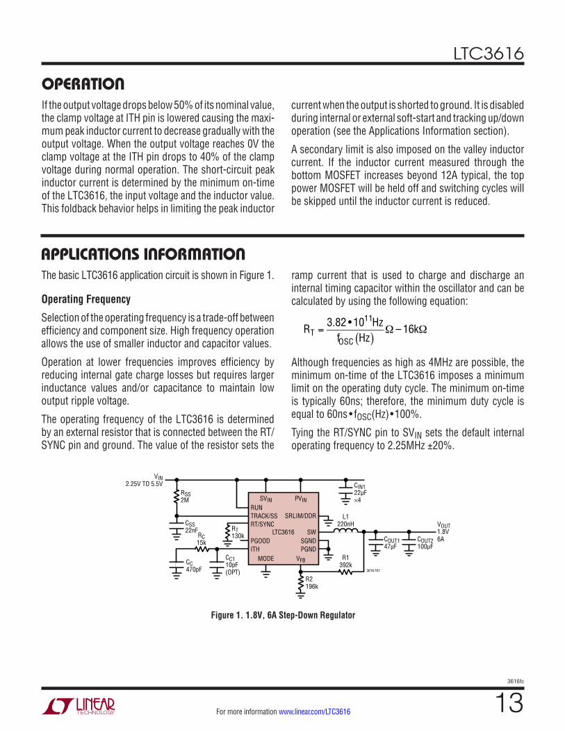
The basic LTC3616 application circuit is shown in Figure 1.
Operating Frequency
Selection of the operating frequency is a trade-off between efficiency and component size. High frequency operation allows the use of smaller inductor and capacitor values.
Operation at lower frequencies improves efficiency by reducing internal gate charge losses but requires larger inductance values and/or capacitance to maintain low output ripple voltage.
The operating frequency of the LTC3616 is determined by an external resistor that is connected between the RT/SYNC pin and ground. The value of the resistor sets the
RUNTRACK/SSRT/SYNC
PGOODITH
SGNDPGND
VIN2.25V TO 5.5V
SRLIM/DDR
SVIN
LTC3616 SW
PVIN
CIN122µF×4
CC470pF
CSS22nF
L1220nH
R1392k
R2196k
3616 F01
MODE VFB
COUT147µF
COUT2100µF
VOUT1.8V6ARC
15k
RT130k
RSS2M
CC110pF(OPT)
Figure 1. 1.8V, 6A Step-Down Regulator
ramp current that is used to charge and discharge an internal timing capacitor within the oscillator and can be calculated by using the following equation:
RT =
3.82 • 1011HzfOSC Hz( )
Ω – 16kΩ
Although frequencies as high as 4MHz are possible, the minimum on-time of the LTC3616 imposes a minimum limit on the operating duty cycle. The minimum on-time is typically 60ns; therefore, the minimum duty cycle is equal to 60ns • fOSC(Hz) •100%.
Tying the RT/SYNC pin to SVIN sets the default internal operating frequency to 2.25MHz ±20%.

LTC3616
143616fc
For more information www.linear.com/LTC3616
applicaTions inForMaTionFrequency Synchronization
The LTC3616’s internal oscillator can be synchronized to an external frequency by applying a square wave clock signal to the RT/SYNC pin. During synchronization, the top switch turn-on is locked to the falling edge of the external frequency source. The synchronization frequency range is 300kHz to 4MHz. During synchronization all operation modes can be selected.
It is recommended that the regulator is powered down (RUN pin to ground) before removing the clock signal on the RT/SYNC pin in order to reduce inductor current ripple.
AC coupling should be used if the external clock generator cannot provide a continuous clock signal throughout start-up, operation and shutdown of the LTC3616. The size of capacitor CSYNC depends on parasitic capacitance on the RT/SYNC pin and is typically in the range of 10pF to 22pF.
Inductor Selection
For a given input and output voltage, the inductor value and operating frequency determine the ripple current. The ripple current ∆IL increases with higher VIN and decreases with higher inductance:
∆IL =
VOUTfSW •L
⎛
⎝⎜
⎞
⎠⎟ • 1–
VOUTVIN
⎛
⎝⎜
⎞
⎠⎟
Having a lower ripple current reduces the core losses in the inductor, the ESR losses in the output capacitors and the output voltage ripple. A reasonable starting point for selecting the ripple current is ∆IL = 0.3 • IOUT(MAX). The largest ripple current occurs at the highest VIN. To guarantee that the ripple current stays below a specified maximum, the inductor value should be chosen according to the following equation:
L =
VOUTfSW • ∆IL(MAX)
⎛
⎝⎜⎜
⎞
⎠⎟⎟ • 1–
VOUTVIN
⎛
⎝⎜
⎞
⎠⎟
The inductor value will also have an effect on Burst Mode operation. The transition to low current operation begins when the peak inductor current falls below a level set by the burst clamp. Lower inductor values result in higher ripple current which causes this to occur at lower load currents. This causes a dip in efficiency in the upper range of low current operation. In Burst Mode operation, lower induc-tance values will cause the burst frequency to increase.
Inductor Core Selection
Once the value for L is known, the type of inductor must be selected. Actual core loss is independent of core size for fixed inductor value, but it is very dependent on the induc-tance selected. As the inductance increases, core losses de-crease. Unfortunately, increased inductance requires more turns of wire and therefore, copper losses will increase.
LTC3616SVIN
VIN
RT/SYNC
LTC3616SVIN
VIN
0.4VRT/SYNC
RT
RT
SGND
LTC3616SVIN
fOSC2.25MHz
fOSC1/TP
fOSC ∝1/RT
VIN
RT/SYNCSGND
TP
1.2V0.3V
LTC3616SVIN fOSC
1/TP
VIN
CSYNC
RT/SYNCSGND
3616 F02
Figure 2. Setting the Switching Frequency

LTC3616
153616fc
For more information www.linear.com/LTC3616
applicaTions inForMaTionFerrite designs have very low core losses and are pre-ferred at high switching frequencies, so design goals can concentrate on copper loss and preventing satura-tion. Ferrite core material saturates “hard,” meaning that inductance collapses abruptly when the peak design current is exceeded. This results in an abrupt increase in inductor ripple current and consequently output voltage ripple. Do not allow a ferrite core to saturate and select external inductors respecting the temperature range of the application!
Different core materials and shapes will change the size/current and price/current relationship of an inductor. Toroid or shielded pot cores in ferrite or permalloy materials are small and don’t radiate much energy, but generally cost more than powdered iron core inductors with similar characteristics. The choice of which style inductor to use mainly depends on the price versus size requirements and any radiated field/EMI requirements. Table 1 shows some typical surface mount inductors that work well in LTC3616 applications.
Input Capacitor (CIN) Selection
In continuous mode, the source current of the top P-channel MOSFET is a square wave of duty cycle VOUT/VIN. To prevent large voltage transients, a low ESR capacitor sized for the maximum RMS current must be used at VIN.
The maximum RMS capacitor current is given by:
IRMS = IOUT(MAX) •
VOUTVIN
• VINVOUT
– 1⎛
⎝⎜
⎞
⎠⎟
This formula has a maximum at VIN = 2VOUT , where IRMS = IOUT/2. This simple worst-case condition is commonly used for design because even significant deviations do not offer much relief. Note that ripple current ratings from capacitor manufacturers are often based on only 2000 hours of life which makes it advisable to further derate the capacitor, or choose a capacitor rated at a higher temperature than required. Generally select the capacitors respecting the temperature range of the application! Several capacitors may also be paralleled to meet size or height requirements in the design.
Table 1. Representative Surface Mount InductorsINDUCTANCE
(μH)DCR (mΩ)
MAX CURRENT (A)
DIMENSIONS (mm)
HEIGHT (mm)
Vishay IHLP-2525CZ-01
0.10 1.5 60 6.5 × 6.9 3
0.15 1.9 52 6.5 × 6.9 3
0.20 2.4 41 6.5 × 6.9 3
0.22 2.5 40 6.5 × 6.9 3
0.33 3.5 30 6.5 × 6.9 3
0.47 4 26 6.5 × 6.9 3
Sumida CDMC6D28 Series
0.2 2.5 21.7 7.25 × 4.4 3
0.3 3.2 15.4 7.25 × 4.4 3
0.47 4.2 13.6 7.25 × 4.4 3
Cooper HCP0703 Series
0.22 2.8 23 7 × 7.3 3.0
0.47 4.2 17 7 × 7.3 3.0
0.68 5.5 15 7 × 7.3 3.0
Würth Electronik WE-HC744312 Series
0.25 2.5 18 7 × 7.7 3.8
0.47 3.4 16 7 × 7.7 3.8
Coilcraft SLC7530 Series
0.100 0.123 20 7.5 × 6.7 3
0.188 0.100 21 7.5 × 6.7 3
0.272 0.100 14 7.5 × 6.7 3
0.350 0.100 11 7.5 × 6.7 3
0.400 0.100 8 7.5 × 6.7 3

LTC3616
163616fc
For more information www.linear.com/LTC3616
applicaTions inForMaTionOutput Capacitor (COUT ) Selection
The selection of COUT is typically driven by the required ESR to minimize voltage ripple and load step transients (low ESR ceramic capacitors are discussed in the next section). Typically, once the ESR requirement is satisfied, the capacitance is adequate for filtering. The output ripple ∆VOUT is determined by:
∆VOUT ≤ ∆IL • ESR+
18 • fSW • COUT
⎛
⎝⎜
⎞
⎠⎟
where fOSC = operating frequency, COUT = output capaci-tance and ∆IL = ripple current in the inductor. The output ripple is highest at maximum input voltage since ∆IL increases with input voltage.
In surface mount applications, multiple capacitors may have to be paralleled to meet the capacitance, ESR or RMS current handling requirement of the application. Aluminum electrolytic, special polymer, ceramic and dry tantalum capacitors are all available in surface mount packages.
Tantalum capacitors have the highest capacitance density, but can have higher ESR and must be surge tested for use in switching power supplies. Aluminum electrolytic capacitors have significantly higher ESR, but can often be used in extremely cost-sensitive applications provided that consideration is given to ripple current ratings and long-term reliability.
Ceramic Input and Output Capacitors
Ceramic capacitors have the lowest ESR and can be cost effective, but also have the lowest capacitance density, high voltage and temperature coefficients, and exhibit audible piezoelectric effects. In addition, the high Q of ceramic capacitors along with trace inductance can lead to significant ringing.
They are attractive for switching regulator use because of their very low ESR, but great care must be taken when using only ceramic input and output capacitors.
Ceramic capacitors are prone to temperature effects which require the designer to check loop stability over the operating temperature range. To minimize their large temperature and voltage coefficients, only X5R or X7R ceramic capacitors should be used.
When a ceramic capacitor is used at the input and the power is being supplied through long wires, such as from a wall adapter, a load step at the output can induce ringing at the VIN pin. At best, this ringing can couple to the output and be mistaken as loop instability. At worst, the ringing at the input can be large enough to damage the part.
Since the ESR of a ceramic capacitor is so low, the input and output capacitor must instead fulfill a charge storage requirement. During a load step, the output capacitor must instantaneously supply the current to support the load until the feedback loop raises the switch current enough to sup-port the load. The time required for the feedback loop to respond is dependent on the compensation components and the output capacitor size. Typically, 3 to 4 cycles are required to respond to a load step, but only in the first cycle does the output drop linearly. The output droop, VDROOP , is usually about 2 to 4 times the linear drop of the first cycle; however, this behavior can vary depending on the compensation component values. Thus, a good place to start is with the output capacitor size of approximately:
COUT ≈
3.5 • ∆IOUTfSW • VDROOP
This is only an approximation; more capacitance may be needed depending on the duty cycle and load step requirements.
In most applications, the input capacitor is merely required to supply high frequency bypassing, since the impedance to the supply is very low.

LTC3616
173616fc
For more information www.linear.com/LTC3616
Output Voltage Programming
The output voltage is set by an external resistive divider according to the following equation:
VOUT = 0.6 • 1+
R1R2
⎛
⎝⎜
⎞
⎠⎟ V
The resistive divider allows pin VFB to sense a fraction of the output voltage as shown in Figure 1.
Burst Clamp Programming
If the voltage on the MODE pin is less than 0.8V, Burst Mode operation is enabled.
If the voltage on the MODE pin is less than 0.3V, the in-ternal default burst clamp level is selected. The minimum voltage on the ITH pin is typically 525mV (internal clamp).
If the voltage is between 0.45V and 0.8V, the voltage on the MODE pin (VBURST) is equal to the minimum voltage on the ITH pin (external clamp) and determines the burst clamp level IBURST (typically from 0A to 7A).
When the ITH voltage falls below the internal (or external) clamp voltage, the sleep state is enabled.
As the output load current drops, the peak inductor current decreases to keep the output voltage in regulation. When the output load current demands a peak inductor current that is less than IBURST , the burst clamp will force the peak inductor current to remain equal to IBURST regardless of further reductions in the load current.
Since the average inductor current is greater than the out-put load current, the voltage on the ITH pin will decrease. When the ITH voltage drops, sleep mode is enabled in which both power switches are shut off along with most of the circuitry to minimize power consumption. All cir-cuitry is turned back on and the power switches resume operation when the output voltage drops out of regulation. The value for IBURST is determined by the desired amount of output voltage ripple. As the value of IBURST increases, the sleep period between pulses and the output voltage ripple increase. Note that for very high VBURST voltage settings, the power good comparator may trip, since the output ripple may get bigger than the power good window.
Pulse-skipping mode, which is a compromise between low output voltage ripple and efficiency, can be implemented by connecting MODE to SVIN. This sets IBURST to 0A. In this condition, the peak inductor current is limited by the minimum on-time of the current comparator. The low-est output voltage ripple is achieved while still operating discontinuously. During very light output loads, pulse-skipping allows only a few switching cycles to skip while maintaining the output voltage in regulation.
Internal and External Compensation
The regulator loop response can be checked by looking at the load current transient response. Switching regulators take several cycles to respond to a step in DC load current. When a load step occurs, VOUT shifts by an amount equal to ∆ILOAD(ESR), where ESR is the effective series resistance of COUT . ∆ILOAD also begins to charge or discharge COUT , generating the feedback error signal that forces the regula-tor to adapt to the current change and return VOUT to its steady-state value. During this recovery time VOUT can be monitored for excessive overshoot or ringing, which would indicate a stability problem. The availability of the ITH pin allows the transient response to be optimized over a wide range of output capacitance.
The ITH external components (RC and CC) shown in Fig-ure 1 provide adequate compensation as a starting point for most applications. The values can be modified slightly to optimize transient response once the final PCB layout is done and the particular output capacitor type and value have been determined. The output capacitors need to be selected because the various types and values determine the loop gain and phase. The gain of the loop will be in-creased by increasing RC and the bandwidth of the loop will be increased by decreasing CC. If RC is increased by the same factor that CC is decreased, the zero frequency will be kept the same, thereby keeping the phase shift the same in the most critical frequency range of the feedback loop. The output voltage settling behavior is related to the stability of the closed-loop system. The external capaci-tor, CC1, (Figure 1) is not needed for loop stability, but it helps filter out any high frequency noise that may couple onto that node.
applicaTions inForMaTion

LTC3616
183616fc
For more information www.linear.com/LTC3616
A second, more severe transient is caused by switching in loads with large (>1μF) supply bypass capacitors. The discharged bypass capacitors are effectively put in parallel with COUT , causing a rapid drop in VOUT . No regulator can alter its delivery of current quickly enough to prevent this sudden step change in output voltage if the load switch resistance is low and it is driven quickly. More output capacitance may be required depending on the duty cycle and load step requirements.
AVP Mode
Fast load transient response, limited board space and low cost are typical requirements of microprocessor power supplies. A microprocessor has typical full load step with very fast slew rate. The voltage at the microprocessor must be held to about ±0.1V of nominal in spite of these load current steps. Since the control loop cannot respond this fast, the output capacitors must supply the load current until the control loop can respond.
Normally, several capacitors in parallel are required to meet microprocessor transient requirements. Capacitor ESR and ESL primarily determine the amount of droop or overshoot in the output voltage.
Consider the LTC3616 without AVP with a bank of tantalum output capacitors. If a load step with very fast slew rate occurs, the voltage excursion will be seen in both direc-tions, for full load to minimum load transient and for the minimum load to full load transient.
applicaTions inForMaTion
Figure 4. Load Step Transient Forced Continuous Mode with AVP Mode
If the ITH pin is tied to SVIN, the active voltage position-ing (AVP) mode and internal compensation are selected.
AVP mode intentionally compromises load regulation by reducing the gain of the feedback circuit, resulting in an output voltage that varies with load current. When the load current suddenly increases, the output voltage starts from a level slightly higher than nominal so the output voltage can droop more and stay within the specified voltage range. When the load current suddenly decreases the output voltage starts at a level lower than nominal so the output voltage can have more overshoot and stay within the specified voltage range (see Figures 3 and 4).
The benefit is a lower peak-to-peak output voltage deviation for a given load step without having to increase the output filter capacitance. Alternatively, the output voltage filter capacitance can be reduced while maintaining the same peak to peak transient response. Due to the reduced loop gain in AVP mode, no external compensation is required.
DDR Mode
The LTC3616 can both source and sink current if the MODE pin is configured to forced continuous mode.
Current sinking is typically limited to 3A for 1MHz frequency and a 0.47µH inductor, but can be lower at higher frequen-cies and low output voltages. If higher ripple current can be tolerated, smaller inductor values can increase the sink current limit. See the Typical Performance Characteristics curves for more information.
Figure 3. Load Step Transient Forced Continuous Mode (AVP Inactive)
VOUT200mV/DIV
IL1A/DIV
50µs/DIV 3616 F03VIN = 3.3VVOUT = 1.8VILOAD = 100mA TO 3AVMODE = 1.5VCOMPENSATION FIGURE 1
VOUT100mV/DIV
IL1A/DIV
50µs/DIV 3616 F04VIN = 3.3VVOUT = 1.8VILOAD = 100mA TO 3AVMODE = 1.5VVITH = 3.3VOUTPUT CAPACITOR VALUE FIGURE 1

LTC3616
193616fc
For more information www.linear.com/LTC3616
applicaTions inForMaTionIn addition, tying the SRLIM/DDR pin to SVIN, lower external reference voltage and tracking output voltage between channels are possible. See the Output Voltage Tracking and External Reference Input sections.
Soft-Start
The RUN pin provides a means to shut down the LTC3616. Tying the RUN pin to SGND places the LTC3616 in a low quiescent current shutdown state (IQ < 1µA).
When the LTC3616 is enabled by pulling the RUN pin high, the chip enters a soft start-up state. The type of soft start-up behavior is set by the TRACK/SS pin:
1. Tying TRACK/SS to SVIN selects the internal soft-start circuit. This circuit ramps the output voltage to the final value within 1ms.
2. If a longer soft-start period is desired, it can be set externally with a resistor and capacitor on the TRACK/SS pin as shown in Figure 1. The TRACK/SS pin reduces the value of the internal reference at VFB until TRACK/SS is pulled above 0.6V. The external soft-start duration can be calculated by using the following formula:
tSS = RSS • CSS • ln SVIN
SVIN – 0.6V
⎛
⎝⎜
⎞
⎠⎟
3. The TRACK/SS pin can be used to track the output voltage of another supply.
Each time the RUN pin is tied high and the LTC3616 is turned on, the TRACK/SS pin is internally pulled down
for ten microseconds in order to discharge the external capacitor. This discharging time is typically adequate for capacitors up to about 33nF. If a larger capacitor is required, connect the external soft-start resistor to the RUN pin.
Regardless of either internal or external soft-start state, the MODE pin is ignored and soft-start will always be in pulse-skipping mode. In addition, the PGOOD pin is kept low and foldback of the switching frequency is disabled.
Programmable Switch Pin Slew Rate
As switching frequencies rise, it is desirable to minimize the transition time required when switching to minimize power losses and blanking time for the switch to settle. However, fast slewing of the switch node results in relatively high external radiated EMI and high on chip supply transients, which can cause problems for some applications.
The LTC3616 allows the user to control the slew rate of the switching node SW by using the SRLIM/DDR pin. Tying this pin to ground selects the fastest slew rate. The slowest slew rate is selected when the pin is open. Con-necting a resistor (between 10k and 100k) from SRLIM pin to ground adjusts the slew rate between the maximum and minimum values. The reduced dV/dt of the switch node results in a significant reduction of the supply and ground ringing, as well as lower radiated EMI.
Particular attention should be used with very high switching frequencies. Using the slowest slew rate (SRLIM open) can reduce the minimum duty cycle capability.
Figure 5. Slew Rate at SW Pin vs SRLIM/DDR Resistor: Open, 100k, 10k
2ns/DIV
SW P
IN
SW P
IN
10k100k
OPEN
3616 F05VIN = 3.3VVOUT = 1.8VfSW = 2.25MHz
2ns/DIVVIN = 3.3VVOUT = 1.8VfSW = 2.25MHz
10k
100k
OPEN

LTC3616
203616fc
For more information www.linear.com/LTC3616
applicaTions inForMaTionOutput Voltage Tracking Input
If the DDR pin is not tied to SVIN, once VTRACK/SS exceeds 0.6V, the run state is entered and the MODE selection, power good and current foldback circuits are enabled.
In the run state, the TRACK/SS pin can be used for track-ing down/up the output voltage of another supply. If the VTRACK/SS drops below 0.6V, the LTC3616 enters the down tracking state and VOUT is referenced to the TRACK/SS voltage. If the TRACK/SS pin drops below 0.2V, the switching frequency is reduced to ensure that the mini-mum duty cycle limit does not prevent the output from following the TRACK/SS pin. The run state will resume if VTRACK/SS again exceeds 0.6V and VOUT is referenced to the internal precision reference (see Figure 8).
Through the TRACK/SS pin, the output voltage can be set up for either coincident or ratiometric tracking, as shown in Figure 6.
To implement the coincident tracking behavior in Fig-ure 6a, connect an extra resistive divider to the output of the master channel and connect its midpoint to the TRACK/SS pin for the slave channel. The ratio of this divider should be selected to be the same as that of the slave channel’s feedback divider (Figure 7a). In this track-ing mode, the master channel’s output must be set higher than slave channel’s output. To implement the ratiometric tracking behavior in Figure 6b, different resistor divider values must be used as specified in Figure 7b.
For coincident start-up, the voltage value at the TRACK/SS pin for the slave channel needs to reach the final reference value after the internal soft-start time (around 1ms). The master start-up time needs to be adjusted with an external capacitor and resistor to ensure this.
External Reference Input (DDR Mode)
If the DDR pin is tied to SVIN (DDR mode), the run state is entered when VTRACK/SS exceeds 0.3V and tracking down behavior is possible if the VTRACK/SS voltage is below 0.6V.
This allows TRACK/SS to be used as an external reference between 0.3V and 0.6V if desired. During the run state in DDR mode, the power good window moves in relation
Figure 7a. Setup for Coincident Tracking
Figure 7b. Setup for Ratiometric Tracking
VFB2
R4
R2
R4
R2
R3
R2
R4 ≤ R3
VOUT2VOUT1
LTC3616
TRACK/SS2
VFB1VIN
LTC3616
LTC3616 CHANNEL 2SLAVE
LTC3616 CHANNEL 1MASTER
TRACK/SS1
3616 F07a
VFB2
R1
R2
R5
R6
R3 R1/R2 < R5/R6
R4
VOUT2VOUT1
LTC3616
TRACK/SS2
VFB1
VIN
3616 F07b
LTC3616
LTC3616 CHANNEL 2SLAVE
LTC3616 CHANNEL 1MASTER
TRACK/SS1
Figure 6. Two Different Modes of Output Voltage Tracking
TIME
(6b) Ratiometric Tracking
VOUT1
VOUT2
OUTP
UT V
OLTA
GE
TIME3616 F06
(6a) Coincident Tracking
VOUT1
VOUT2
OUTP
UT V
OLTA
GE

LTC3616
213616fc
For more information www.linear.com/LTC3616
to the actual TRACK/SS pin voltage if the voltage value is between 0.3V and 0.6V. Note: if TRACK/SS voltage is 0.6V, either the tracking circuit or the internal reference can be used.
During up/down tracking the output current foldback is disabled and the PGOOD pin is always pulled down (see Figure 9).
applicaTions inForMaTion
Figure 8. DDR Pin Not Tied to SVIN
Figure 9. DDR Pin Tied to SVIN. Example DDR Application
SOFT-STARTSTATE
tSS > 1ms
SHUTDOWNSTATE
0.6V
0.6V
0.2V
0V
0V
0V
0V
VIN
VIN
VFB PINVOLTAGE
TRACK/SSPIN VOLTAGE
RUN PINVOLTAGE
SVIN PINVOLTAGE
RUN STATE RUN STATE
TIME
3616 F08
REDUCEDSWITCHINGFREQUENCY
DOWNTRACKINGSTATE
UPTRACKING
STATE
SOFT-STARTSTATE
tSS > 1ms
SHUTDOWNSTATE
0.3V0.45V
0.45V0.3V0.2V
0V
0V
0V
0V
VIN
VIN
VFB PINVOLTAGE
EXTERNALVOLTAGE
REFERENCE 0.45V
TRACK/SSPIN VOLTAGE
RUN PINVOLTAGE
SVIN PINVOLTAGE
RUN STATE RUN STATE
TIME
3616 F09
REDUCEDSWITCHINGFREQUENCY
DOWNTRACKINGSTATE
UPTRACKING
STATE
Efficiency Considerations
The efficiency of a switching regulator is equal to the output power divided by the input power times 100%. It is often useful to analyze individual losses to determine what is limiting the efficiency and which change would produce the most improvement. Efficiency can be expressed as:
Efficiency = 100% – (L1 + L2 + L3 + ...)
where L1, L2, etc. are the individual losses as a percent-age of input power.

LTC3616
223616fc
For more information www.linear.com/LTC3616
Although all dissipative elements in the circuit produce losses, two main sources usually account for most of the losses: VIN quiescent current and I2R losses. The VIN quiescent current loss dominates the efficiency loss at very low load currents whereas the I2R loss dominates the efficiency loss at medium to high load currents. In a typical efficiency plot, the efficiency curve at very low load currents can be misleading since the actual power lost is usually of no consequence.
1. The VIN quiescent current is due to two components: the DC bias current as given in the Electrical Characteristics and the internal main switch and synchronous switch gate charge currents. The gate charge current results from switching the gate capacitance of the internal power MOSFET switches. Each time the gate is switched from low to high to low again, a packet of charge dQ moves from VIN to ground. The resulting dQ/dt is the current out of VIN due to gate charge, and it is typically larger than the DC bias current. Both the DC bias and gate charge losses are proportional to VIN; thus, their effects will be more pronounced at higher supply voltages.
2. I2R losses are calculated from the resistances of the internal switches, RSW , and external inductor, RL. In continuous mode the average output current flowing through inductor L is “chopped” between the main switch and the synchronous switch. Thus, the series resistance looking into the SW pin is a function of both top and bottom MOSFET RDS(ON) and the duty cycle (DC) as follows:
RSW = (RDS(ON)TOP)(DC) + (RDS(ON)BOT)(1 – DC)
The RDS(ON) for both the top and bottom MOSFETs can be obtained from the Typical Performance Character-istics curves. To obtain I2R losses, simply add RSW to RL and multiply the result by the square of the average output current.
Other losses including CIN and COUT ESR dissipative losses and inductor core losses generally account for less than 2% of the total loss.
Thermal Considerations
In most applications, the LTC3616 does not dissipate much heat due to its high efficiency.
However, in applications where the LTC3616 is running at high ambient temperature with low supply voltage and high duty cycles, such as in dropout, the heat dissipated may exceed the maximum junction temperature of the part. If the junction temperature reaches approximately 170°C, both power switches will be turned off and the SW node will become high impedance.
To prevent the LTC3616 from exceeding the maximum junction temperature, some thermal analysis is required. The temperature rise is given by:
TRISE = (PD)(θJA)
where PD is the power dissipated by the regulator and θJA is the thermal resistance from the junction of the die to the ambient temperature. The junction temperature, TJ, is given by:
TJ = TA + TRISE
where TA is the ambient temperature.
As an example, consider the case when the LTC3616 is in dropout at an input voltage of 3.3V with a load current of 6A at an ambient temperature of 70°C. From the Typical Performance Characteristics graph of Switch Resistance, the RDS(ON) resistance of the P-channel switch is 0.035Ω. Therefore, power dissipated by the part is:
PD = (IOUT)2 • RDS(ON) = 1.26W
For the QFN package, the θJA is 38°C/W.
Therefore, the junction temperature of the regulator op-erating at 70°C ambient temperature is approximately:
TJ = 1.26W • 38°C/W + 70°C = 118°C
We can safely assume that the actual junction temperature will not exceed the absolute maximum junction tempera-ture of 125°C.
Note that for very low input voltage, the junction tempera-ture will be higher due to increased switch resistance, RDS(ON). It is not recommended to use full load current for high ambient temperature and low input voltage.
To maximize the thermal performance of the LTC3616 the exposed pad should be soldered to a ground plane. See the PCB Layout Board Checklist.
applicaTions inForMaTion
LTC3616
233616fc
For more information www.linear.com/LTC3616
applicaTions inForMaTionDesign Example
As a design example, consider using the LTC3616 in an application with the following specifications:
VIN = 2.25V to 5.5V, VOUT = 1.8V, IOUT(MAX) = 6A, IOUT(MIN) = 200mA, f = 2.6MHz.
Efficiency is important at both high and low load current, so Burst Mode operation will be utilized.
First, calculate the timing resistor:
RT =
3.8211Hz2.6MHz
k – 16k = 130kΩ
Next, calculate the inductor value for about 30% ripple current at maximum VIN:
L =
1.8V2.6MHz • 2A
⎛
⎝⎜
⎞
⎠⎟ • 1– 1.8V
5.5V⎛
⎝⎜
⎞
⎠⎟ = 0.233µH
Using a standard value of 0.22µH inductor results in a maximum ripple current of:
∆IL =
1.8V2.6MHz • 0.22µH
⎛
⎝⎜
⎞
⎠⎟ • 1– 1.8V
5.5V⎛
⎝⎜
⎞
⎠⎟ = 2.12A
COUT will be selected based on the ESR that is required to satisfy the output voltage ripple requirement and the bulk capacitance needed for loop stability. For this design, a 150µF (or 47µF plus 100µF) ceramic capacitor is used with a X5R or X7R dielectric.
Assuming worst-case conditions of VIN = 2VOUT, CIN should be selected for a maximum current rating of:
IRMS = 6A • 1.8V
3.6V• 3.6V
1.8V– 1
⎛
⎝⎜
⎞
⎠⎟ = 3ARMS
Decoupling PVIN with four 22µF capacitors is adequate for most applications.
If we set R2 = 196k, the value of R1 can now be determined by solving the following equation.
R1 = 196k • 1.8V
0.6V−1
⎛
⎝⎜
⎞
⎠⎟
A value of 392k will be selected for R1.
Finally, define the soft start-up time choosing the proper value for the capacitor and the resistor connected to TRACK/SS. If we set minimum tSS = 5ms and a resistor of 2MΩ, the following equation can be solved with the maximum SVIN = 5.5V :
CSS =5ms
2MΩ • In 5.5V5.5V – 0.6V
⎛
⎝⎜
⎞
⎠⎟
= 21.6nF
The standard value of 22nF guarantees the minimum soft-start up time of 5ms.
Figure 1 shows the schematic for this design example.
PC Board Layout Checklist
When laying out the printed circuit board, the following checklist should be used to ensure proper operation of the LTC3616:
1. A ground plane is recommended. If a ground plane layer is not used, the signal and power grounds should be segregated with all small-signal components returning to the SGND pin at one point which is then connected to the PGND pin close to the LTC3616.
2. Connect the (+) terminal of the input capacitor(s), CIN, as close as possible to the PVIN pin, and the (–) terminal as close as possible to the exposed pad, PGND. This capacitor provides the AC current into the internal power MOSFETs.
3. Keep the switching node, SW, away from all sensitive small-signal nodes.
4. Flood all unused areas on all layers with copper. Flood-ing with copper will reduce the temperature rise of power components. Connect the copper areas to PGND (exposed pad) for best performance.
5. Connect the VFB pin directly to the feedback resistors. The resistor divider must be connected between VOUT and SGND.

LTC3616
243616fc
For more information www.linear.com/LTC3616
Typical applicaTionsGeneral Purpose Buck Regulator Using Ceramic Capacitors, 2.25MHz
RUNTRACK/SSRT/SYNC
PGOODITH
PGOOD SGNDPGND
VIN2.25V TO 5.5V
SRLIM/DDR
SVIN
LTC3616SW
PVIN
CF1µF
RF24Ω
L10.22µH
R1392k
C322pF
R2196k
3616 TA02a
MODE VFB
CO147µF
CO2100µF
CC110pF
22µF×4
CC470pF
CSS10nF VOUT
1.8V6A
R4100k
R5B1M
L1: VISHAY IHLP-2525CZ-01 220nH
R5A1M
RC15k
RSS4.7M
Efficiency vs Output Current Load Step Forced Continuous Mode
OUTPUT CURRENT (mA)
30
EFFI
CIEN
CY (%
)
90
100
20
10
80
50
70
60
40
1 100 1000 10000
3616 TA02b
010
VIN = 2.5VVIN = 3.3VVIN = 4VVIN = 5.5V
VOUT = 1.8V, VIN = 3.3V
VOUT200mV/DIV
IOUT5A/DIV
50µs/DIV 3616 TA02cVIN = 3.3VVOUT = 1.8VIOUT = 100mA TO 3AVMODE = 1.5V

LTC3616
253616fc
For more information www.linear.com/LTC3616
Typical applicaTionsMaster and Slave for Coincident Tracking Outputs Using a 1MHz External Clock
RUNTRACK/SSRT/SYNC
PGOODITH
PGOOD SGNDPGND
VIN2.25V TO 5.5V
SRLIM/DDR
SVIN
LTC3616SW
PVIN
CF11µF
RF124Ω
L10.47µH
CHANNEL 1MASTER
CHANNEL 2SLAVE
R1715k
C322pF
R2357k
R3464k
R4464k
3616 TA03a
MODE VFB
CO1147µF
CO12100µF
CC210pF
22µF×4
CC1470pF
VOUT11.8V6A
10nF
4.7M
4.7M
4.7M
R5100k
1MHzCLOCK
RC115k
RUNTRACK/SSRT/SYNC
PGOODITH
PGOOD SGNDPGND
SRLIM/DDR
SVIN
LTC3616SW
PVIN
CF21µF
RF224Ω
L20.47µH
R5301k
C722pF
R6301k
MODE VFB
CO2147µF
CO22100µF
CC410pF
L1, L2: VISHAY IHLP-2525CZ-01 470nH
22µF×4
CC3470pF
VOUT21.2V6A
R7100kRC2
15k
Coincident Start-Up Coincident Tracking Up/Down
500mV/DIV
2ms/DIV 3616 TA03b
VOUT1
VOUT2
500mV/DIV
200ms/DIV 3616 TA03c
VOUT1
VOUT2
LTC3616
263616fc
For more information www.linear.com/LTC3616
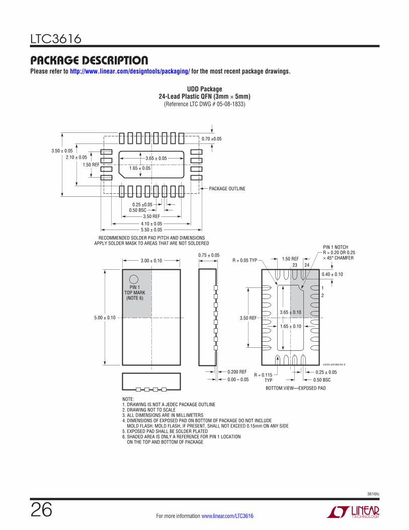
package DescripTion
UDD Package24-Lead Plastic QFN (3mm × 5mm)
(Reference LTC DWG # 05-08-1833)
3.00 ± 0.10 1.50 REF
5.00 ± 0.10
NOTE:1. DRAWING IS NOT A JEDEC PACKAGE OUTLINE2. DRAWING NOT TO SCALE3. ALL DIMENSIONS ARE IN MILLIMETERS4. DIMENSIONS OF EXPOSED PAD ON BOTTOM OF PACKAGE DO NOT INCLUDE MOLD FLASH. MOLD FLASH, IF PRESENT, SHALL NOT EXCEED 0.15mm ON ANY SIDE5. EXPOSED PAD SHALL BE SOLDER PLATED6. SHADED AREA IS ONLY A REFERENCE FOR PIN 1 LOCATION ON THE TOP AND BOTTOM OF PACKAGE
PIN 1TOP MARK(NOTE 6)
0.40 ± 0.10
23 24
1
2
BOTTOM VIEW—EXPOSED PAD
3.50 REF
0.75 ± 0.05
R = 0.115TYP
PIN 1 NOTCHR = 0.20 OR 0.25× 45° CHAMFER
0.25 ± 0.05
0.50 BSC
0.200 REF
0.00 – 0.05
(UDD24) QFN 0808 REV Ø
RECOMMENDED SOLDER PAD PITCH AND DIMENSIONSAPPLY SOLDER MASK TO AREAS THAT ARE NOT SOLDERED
0.70 ±0.05
0.25 ±0.05
3.50 REF
4.10 ± 0.055.50 ± 0.05
1.50 REF
2.10 ± 0.053.50 ± 0.05
PACKAGE OUTLINE
R = 0.05 TYP
1.65 ± 0.10
3.65 ± 0.10
1.65 ± 0.05
UDD Package24-Lead Plastic QFN (3mm × 5mm)
(Reference LTC DWG # 05-08-1833 Rev Ø)
3.65 ± 0.05
0.50 BSC
Please refer to http://www.linear.com/designtools/packaging/ for the most recent package drawings.

LTC3616
273616fc
For more information www.linear.com/LTC3616
Information furnished by Linear Technology Corporation is believed to be accurate and reliable. However, no responsibility is assumed for its use. Linear Technology Corporation makes no representa-tion that the interconnection of its circuits as described herein will not infringe on existing patent rights.
revision hisToryREV DATE DESCRIPTION PAGE NUMBER
A 4/11 Added VRUN specification in the Electrical Characteristics section. 4
B 11/13 Add H and MP grades and applicable temperature range references.Modified Note 2.Modified Typical Performance Characteristics graphs.Modified Inductor Core Selection section.Modified Input Capacitor Selection section.
Throughout4
7, 81515
C 4/14 Modified the top switch current limit specification. 3

LTC3616
283616fc
For more information www.linear.com/LTC3616 LINEAR TECHNOLOGY CORPORATION 2010
LT 0414 REV C • PRINTED IN USALinear Technology Corporation1630 McCarthy Blvd., Milpitas, CA 95035-7417(408) 432-1900 FAX: (408) 434-0507 www.linear.com/LTC3616
relaTeD parTs
Typical applicaTionDDR Termination With Ratiometric Tracking of VDD, 1MHz Ratiometric Start-Up
PART NUMBER DESCRIPTION COMMENTS
LTC3418 5.5V, 8A (IOUT), 4MHz, Synchronous Step-Down DC/DC Converter
95% Efficiency, VIN(MIN) = 2.25V, VIN(MAX) = 5.5V, VOUT(MIN) = 0.8V, IQ = 380µA, ISD <1µA, 5mm × 7mm QFN-38 Package
LTC3415 5.5V, 7A (IOUT), 1.5MHz, Synchronous Step-Down DC/DC Converter
95% Efficiency, VIN(MIN) = 2.5V, VIN(MAX) = 5.5V, VOUT(MIN) = 0.6V, IQ = 450µA, ISD <1µA, 5mm × 7mm QFN-38 Package
LTC3414/ LTC3416
5.5V, 4A (IOUT), 4MHz, Synchronous Step-Down DC/DC Converter
95% Efficiency, VIN(MIN) = 2.25V, VIN(MAX) = 5.5V, VOUT(MIN) = 0.8V, IQ = IQ = 64µA, ISD <1µA, TSSOP20E Package
LTC3413 5.5V, 3A (IOUT Sink/Source), 2MHz, Monolithic Synchronous Regulator for DDR/QDR Memory Termination
90% Efficiency, VIN(MIN) = 2.25V, VIN(MAX) = 5.5V, VOUT(MIN) = VREF/2, IQ = 280µA, ISD <1µA, TSSOP16E Package
LTC3412A 5.5V, 2.5A (IOUT), 4MHz, Synchronous Step-Down DC/DC Converter
95% Efficiency, VIN(MIN) = 2.5V, VIN(MAX) = 5.5V, VOUT(MIN) = 0.8V, IQ = 60µA, ISD <1µA, 4mm × 4mm QFN-16 TSSOP16E Package
LTC3612 5.5V, 3A (IOUT), 4MHz, Synchronous Step-Down DC/DC Converter
95% Efficiency, VIN(MIN) = 2.25V, VIN(MAX) = 5.5V, VOUT(MIN) = 0.6V, IQ = 70µA, ISD <1µA, 3mm × 4mm QFN-20 TSSOP20E Package
RUNTRACK/SSRT/SYNC
PGOODPGOOD
SGNDPGND
VIN3.3V
VDD1.8V SRLIM/DDR
SVIN
LTC3616
SW
PVIN
L10.33µH
R1200k
C322pF
R2200k
3616 TA04a
MODE VFB
C4100µF
C547µF
CC110pF
C122µF×4
CC2.2nF
VTT0.9V±3A
R3100k
R8365k
R51M
L1: COILCRAFT DO3316T
R41M
RC6k
R7187k
R6562k
ITH
500mV/DIV
500µs/DIV 3616 TA04b
VDD
VTT