low-power design enabled by mc9s08qe128 and mcf51qe128 ... · v4 devices, the controller continuum...
TRANSCRIPT
Freescale SemiconductorApplication Note
Document Number: AN3460Rev. 0, 06/2007
ContentsIntroduction . . . . . . . . . . . . . . . . . . . . . . . . . . . . . . . . . . . 1Power vs. Performance . . . . . . . . . . . . . . . . . . . . . . . . . . 2Clock Selection . . . . . . . . . . . . . . . . . . . . . . . . . . . . . . . . 2
3.1 Clock Gating . . . . . . . . . . . . . . . . . . . . . . . . . . . . . . 53.2 Modes of Operation. . . . . . . . . . . . . . . . . . . . . . . . . 93.3 CPU Modes . . . . . . . . . . . . . . . . . . . . . . . . . . . . . . 10Case Study of Smoke Detector . . . . . . . . . . . . . . . . . . . 13Other MCU Features to Help Save Power . . . . . . . . . . 15
5.1 Flash Re-Programming Voltage . . . . . . . . . . . . . . 155.2 Port Manipulation. . . . . . . . . . . . . . . . . . . . . . . . . . 16Conclusion. . . . . . . . . . . . . . . . . . . . . . . . . . . . . . . . . . . 16
Low-Power Design Enabled by MC9S08QE128 and MCF51QE128 Flexis Microcontrollersby Inga Harris
8-Bit Microcontroller Applications EngineerEast Kilbride, Scotland
1 IntroductionSemiconductor manufacturers recognize the need for portable, energy efficient products for both consumer and industrial markets. The battery life of a portable product must increase with each new generation of that product. Energy efficiency ratings for larger products, such as white goods, also must improve with every product generation. The way engineers achieve these goals is by using the features designed into the product. The microcontroller (MCU) plays a central role in power reduction because it both consumes power and controls the other power-consuming components.
From the RS08 to our highest-performance ColdFire® V4 devices, the Controller Continuum provides compatibility for an easy migration path up or down the performance spectrum. The connection point on the Controller Continuum is where complimentary families of S08 and ColdFire V1 (CFV1) microcontrollers share a common set of peripherals and development tools to deliver the ultimate in migration flexibility. Pin-for-pin
123
45
6
© Freescale Semiconductor, Inc., 2007. All rights reserved.
Power vs. Performance
compatibility between many devices allows controller exchanges without redesigning the board. The MC9S08QE128 and the MCF51QE128 are the first products in this series known as Flexis.
The term Flexis means a single development tool to ease migration between 8-bit (S08) and 32-bit (CFV1), a common peripheral set to preserve software investment between 8-bit and 32-bit, and pin compatibility wherever practical to maximize hardware reuse when moving between 8-bit and 32-bit.
This application note explains how to use the power consumption reducing features in the two Flexis QE128 microcontrollers.
NOTE: In the following text, QE128 refers to both MC9S08QE128 and MCF51QE128. If the statement is applicable to one part or the other, then the full part number is used.
2 Power vs. PerformanceIn general terms, the faster components are clocked the more power they consume (the relationship is linear). In applications running over 95% of the time, the MCU solution providing the lowest overall power consumption is the one running as slow as possible in that system. An example of such a system would be a motor controller. If the key function converts a signal via an ADC channel, then due to Nyquist’s law the ADC cannot be clocked at a speed slower than the minimum sample frequency. This limits how slowly the MCU can run.
In many cases, the application performs at the lowest overall power by performing the scheduled tasks as quickly as possible to allow the MCU to go back to a very low power state soon. A smoke detector, for example, only needs to wake every five seconds, take a reading, make a decision, and go back to sleep. (This example is explored further in Section 4, “Case Study of Smoke Detector.”) This method is very common in battery operated devices where systems are in a dormant mode most of the time.
3 Clock SelectionThe heart of the QE128 is the Internal Clock Source Module (ICS), as shown in Figure 1. You can use the ICS module to select an external reference clock (ERCLK) from 32 kHz up to 16 MHz, or an internal reference clock (IRCLK) that is in the range 25 – 41.66 kHz. The heart of the ICS is the Frequency Lock Loop (FLL) block which multiplies its input clock up to a specification maximum of 50 MHz depending upon the modules configuration. The input clock for the FLL, also know as the FLL reference clock, must be in the range of 31.25 – 39.06 kHz for the FLL to operate. Trim the internal clock to the correct range to to meet these specifications. The external reference clock, however, can be as high as 16 MHz and can be divided by a Reference Divider (RDIV) programmable from 1 to 1024 to meet the FLL input clock restrictions. Compared to a PLL, the FLL enables faster stabilization; this allows the application code to start sooner so that changing the FLL frequency is not as large a penalty. The FLL can also be bypassed if a low frequency bus is required. A second divider block, Bus Frequency Divider (BDIV), can divide the clock signal down by 1, 2, 4, or 8, before it is put out on to the ICSOUT signal. The MCU Bus Clock is ICSOUT divided by 2.
Low-Power Design Enabled by MC9S08QE128 and MCF51QE128 Flexis Microcontrollers, Rev. 0
Freescale Semiconductor2

Clock Selection
Figure 1. Internal Clock Source (ICS) Block Diagram
The QE128 devices also have an independent 1 kHz low power oscillator (LPO) which can be used by the Real Time Clock (RTC) and the Watchdog (COP). You can use this feature to conform to EN60730, the standard for automatic electrical controls for household and similar use.
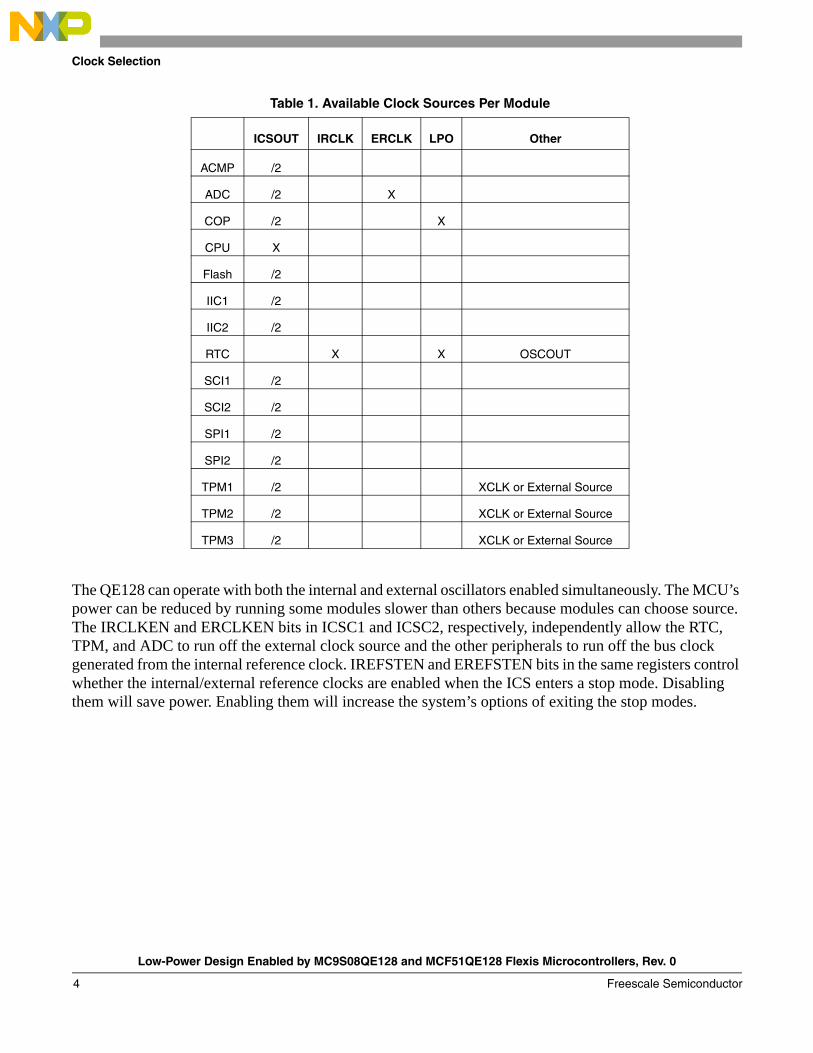
Table 1 shows which clock source can be used by each module on the QE128. The QE128 clock distribution can be seen in Section 1.3 of the device reference manual. Other clocks shown in the table are OSCOUT, which is a direct path to the external clock, and XCLK (also known as ICSFFCLK), which is the signal going into the FLL block (i.e. either the internal oscillator or the external clock source, post-RDIV as shown in Figure 1.)
Low-Power Design Enabled by MC9S08QE128 and MCF51QE128 Flexis Microcontrollers, Rev. 0
Freescale Semiconductor 3
Clock Selection
The QE128 can operate with both the internal and external oscillators enabled simultaneously. The MCU’s power can be reduced by running some modules slower than others because modules can choose source. The IRCLKEN and ERCLKEN bits in ICSC1 and ICSC2, respectively, independently allow the RTC, TPM, and ADC to run off the external clock source and the other peripherals to run off the bus clock generated from the internal reference clock. IREFSTEN and EREFSTEN bits in the same registers control whether the internal/external reference clocks are enabled when the ICS enters a stop mode. Disabling them will save power. Enabling them will increase the system’s options of exiting the stop modes.
Table 1. Available Clock Sources Per Module
ICSOUT IRCLK ERCLK LPO Other
ACMP /2
ADC /2 X
COP /2 X
CPU X
Flash /2
IIC1 /2
IIC2 /2
RTC X X OSCOUT
SCI1 /2
SCI2 /2
SPI1 /2
SPI2 /2
TPM1 /2 XCLK or External Source
TPM2 /2 XCLK or External Source
TPM3 /2 XCLK or External Source
Low-Power Design Enabled by MC9S08QE128 and MCF51QE128 Flexis Microcontrollers, Rev. 0
Freescale Semiconductor4
Clock Selection
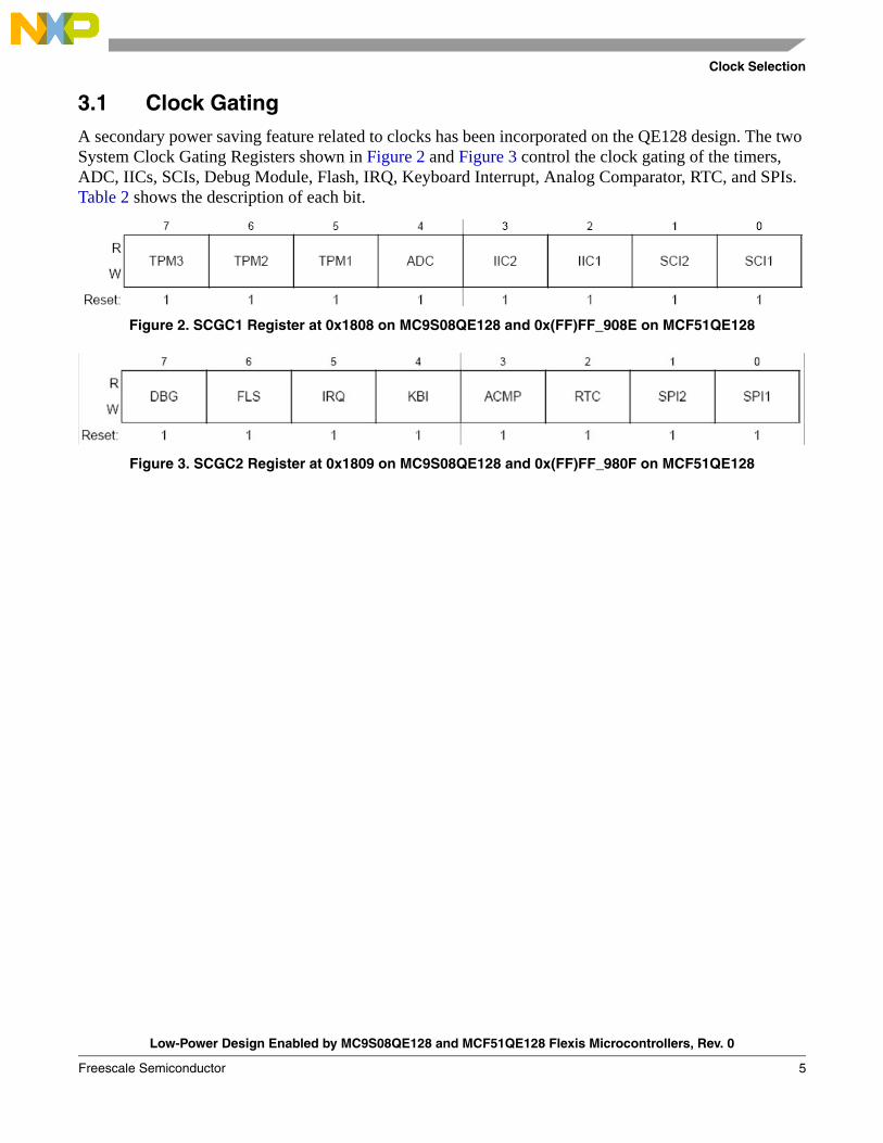
3.1 Clock GatingA secondary power saving feature related to clocks has been incorporated on the QE128 design. The two System Clock Gating Registers shown in Figure 2 and Figure 3 control the clock gating of the timers, ADC, IICs, SCIs, Debug Module, Flash, IRQ, Keyboard Interrupt, Analog Comparator, RTC, and SPIs. Table 2 shows the description of each bit.
Figure 2. SCGC1 Register at 0x1808 on MC9S08QE128 and 0x(FF)FF_908E on MCF51QE128
Figure 3. SCGC2 Register at 0x1809 on MC9S08QE128 and 0x(FF)FF_980F on MCF51QE128
Low-Power Design Enabled by MC9S08QE128 and MCF51QE128 Flexis Microcontrollers, Rev. 0
Freescale Semiconductor 5

Clock Selectiond
Table 2. SCGC2 Register Field Description
By gating off the clock to unused modules, precious micro amps (μA) can be saved in the MCU’s Run and Wait modes. This feature is especially important because of the numerous communications modules and timers incorporated in the QE128. Applications are unlikely to use all of them. Benefits can be found only by gating the modules on in the section of the application that needs them and by gating them off when the job is done. The MC9S08QE128 has five package options: 80-pin LQFP, 64-pin LQFP, 48-pin QFN, 44-pin QFP, and 32-pin LQFP. The MCF51QE128 has two package options: 80-pin LQFP and 64-pin LQFP. All of the packages have peripheral limitations, but this is particularly true for the smaller packages.
Register Field Description
SC
GC
1TPM3
TPM3 Clock Gate Control — This bit controls the clock gate to the TPM3 module.
0 Clock to the module is disabled; 1 Clock to the module is enabled.
TPM2TPM2 Clock Gate Control — This bit controls the clock gate to the TPM2 module.
0 Clock to the module is disabled; 1 Clock to the module is enabled.
TPM1TPM1 Clock Gate Control — This bit controls the clock gate to the TPM1 module.
0 Clock to the module is disabled; 1 Clock to the module is enabled.
ADCADC Clock Gate Control — This bit controls the clock gate to the ADC module.
0 Clock to the module is disabled; 1 Clock to the module is enabled.
IIC2IIC2 Clock Gate Control — This bit controls the clock gate to the IIC2 module.
0 Clock to the module is disabled; 1 Clock to the module is enabled.
IIC1IIC1 Clock Gate Control — This bit controls the clock gate to the IIC1 module.
0 Clock to the module is disabled; 1 Clock to the module is enabled.
SCI2SCI2 Clock Gate Control — This bit controls the clock gate to the SCI2 module.
0 Clock to the module is disabled; 1 Clock to the module is enabled.
SCI1SCI1 Clock Gate Control — This bit controls the clock gate to the SCI1 module.
0 Clock to the module is disabled; 1 Clock to the module is enabled.
SC
GC
2
DBGDBG Clock Gate Control (not available on MCF51QE128) — This bit controls the bus
0 Clock to the module is disabled; 1 Clock to the module is enabled.
FlashFLASH Register Clock Gate Control — This bit controls does not affect normal program execution from with registers is affected.
0 Clock to the module is disabled; 1 Clock to the module is enabled.
IRQIRQ Clock Gate Control — This bit controls the bus
0 Clock to the module is disabled; 1 Clock to the module is enabled.
KBIKBI Clock Gate Control — This bit controls the clock
0 Clock to the module is disabled; 1 Clock to the module is enabled.
ACMPACMP Clock Gate Control — This bit controls the clock gate to both of the ACMP modules.
0 Clock to the module is disabled; 1 Clock to the module is enabled.
RTCRTC Clock Gate Control—This bit controls the bus clock gate to the RTC module. Only the bus clock is gated, the ICSERCLK and LPOCLK are still available to the RTC.
0 Clock to the module is disabled; 1 Clock to the module is enabled.
SPI2SPI2 Clock Gate Control — This bit controls the clock gate to the SPI2 module.
0 Clock to the module is disabled; 1 Clock to the module is enabled.
SPI1SPI1 Clock Gate Control — This bit controls the clock gate to the SPI1 module.
0 Clock to the module is disabled; 1 Clock to the module is enabled.
Low-Power Design Enabled by MC9S08QE128 and MCF51QE128 Flexis Microcontrollers, Rev. 0
Freescale Semiconductor6

Clock Selection
NOTEClock gating may not improve the current consumption if the GPIO pins associated with that function are not configured as output high. Configuring the GPIO as output high is the recommend permutation for unused pins and low power.
3.1.1 Package Differences
The packages available depend on the device selected from the family. Consult the reference manual to learn about the packages available for your device.
NOTEAll unused pins in the application (including, on smaller packages, the GPIO which are not bonded out to the pins) should be pulled up by the internal pull up resistor (PTxPE) if they are set up as inputs or if they should be set up as outputs driving high to keep power consumption down and to improve the application robustness.
3.1.1.1 80-Pin LQFP
The 80-pin LQFP package is the most flexible option. All its modules are bonded out to the pins. But even with 72 application pins (80 minus eight power supply pins), the second SCI (SCI2) and the second analog comparator (ACMP2) share the same pins and therefore cannot be used simultaneously. The QE128 does not have separate clock gating bits for the ACMP modules, but you can assume that all applications will benefit from gating at least one of the modules off.
3.1.1.2 64-Pin LQFP
The 64-pin LQFP package has 16 fewer GPIO pins than the 80-pin package option, four of which were multiplexed with the ADC (channels 20 to 23). This means that from a power saving from clock gating perspective there is no difference.
3.1.1.3 48-Pin QFN
By dropping from the 64 to 48-pin package option, the device cannot use the second IIC (IIC2), ADC channels 10 to 19, and 16 GPIO (some of which were multiplexed). All 48-pin QFN package applications benefit by gating off and disabling IIC2.
3.1.1.4 44-Pin QFP
By dropping from the 48 to the 44-pin package option, the MC9S08QE128 cannot use SPI1 and another four GPIO. All 44-pin QFP package applications will benefit by gating off and disabling SPI1.
3.1.1.5 32-Pin LQFP
The smallest MC9S08QE128 package option is eight GPIO, four KBI, and two TPM external clock sources (TPM2CLK and TPM3CLK) short of the 44-pin option. Its second pair of supply pins (Vss and
Low-Power Design Enabled by MC9S08QE128 and MCF51QE128 Flexis Microcontrollers, Rev. 0
Freescale Semiconductor 7

Clock Selection
Vdd) and the separate Vref pins are also removed. This results in a package without any non-multiplexed GPIO. 32-pin LQFP applications are highly likely to benefit the most from gating the modules on and off when necessary.
3.1.2 Clock Gating Rules
The clock is gated on or off immediately after the register is written. Be careful when using this feature.• After a reset all the clocks are gated on. To keep power consumption down, the clocks should be
gated off as soon as possible.• Writes to registers associated with a gated off module have no effect (e.g. writing to the Modulo of
the RTC module if the SCGC2_RTC bit is 1 will not cause the register value to change).• To avoid errors, disable the module before gating it off and re-initializing the register when the
module is gated back on.
Figure 4 illustrates the power savings attainable by gating off each module. The numbers are indicative of a bench environment running a demo program, and are not characterized or guaranteed by Freescale Semiconductor.
Figure 4. μA Saved Through Clock Gating at 10 MHz Bus in FEE Mode on MC9S08QE128
uA Saving through Clock Gating in Run
ADC220 DBG
230 IIC1200
IIC2200
RTC170
SCI1160
SCI2130
SPI170
SPI280
TPM1190
TPM2180
TPM3300
IRQ40
KBI60
ACMP160
The Rest5050
Flash40
Low-Power Design Enabled by MC9S08QE128 and MCF51QE128 Flexis Microcontrollers, Rev. 0
Freescale Semiconductor8

Clock Selection
3.2 Modes of Operation
3.2.1 Clock Modes
As described earlier, the ICS is routed to all the power consuming and component controlling peripherals. This added flexibility allows designers to choose the appropriate level of power reduction and performance, and can have significant benefits.
All other factors being equal, the low range, low gain external oscillator conserves more power than the internal oscillator circuitry. Bypassing the FLL saves power by reducing the frequency. Disabling (instead of bypassing) the FLL conserves more power.
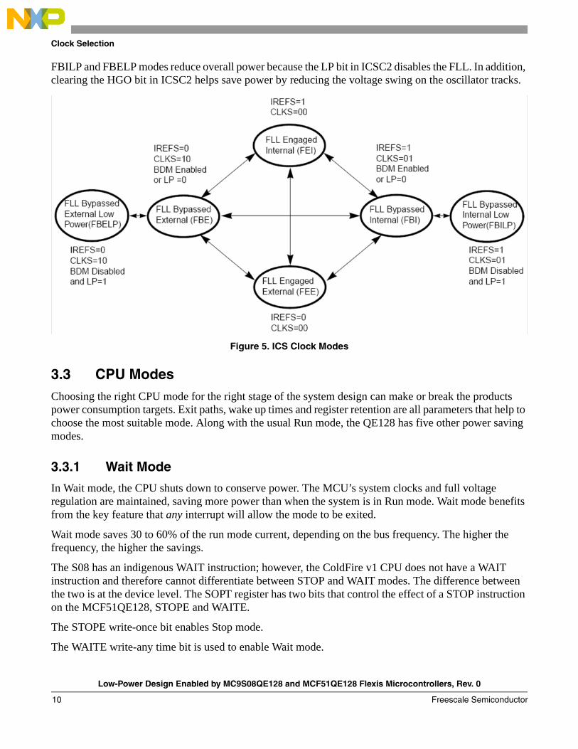
The ICS on the QE128 has six modes of operation:1. FEI (FLL Engaged Internal) is the default mode and is enabled out of reset.
— The ICSOUT signal is derived from the FLL with the internal reference clock selected as the input.
— The default DCO multiplier and BDIV multiplier are 512 and 2, respectively, which means that out of reset the bus clock is 4.19 MHz.
Bus Clock = ( ( Internal Reference Clock x DCO) / BDIV ) / 2— This mode can generate bus clock frequencies from 1 MHz to 25 MHz.
2. FEE (FLL Engaged External)— The RDIV must be used to ensure that the external reference clock signal into the FLL is not
out of the range of 31.25 to 39.0625 kHz.— This mode can generate bus clock frequencies from 1 MHz to 25 MHz.
3. FBI (FLL Bypassed Internal)— ICSOUT is derived from the internal reference and BDIV.— This mode can generate bus clock frequencies from 1.95 to 19.6 kHz.
4. FBE (FLL Bypassed External)— ICSOUT is derived from the external reference and BDIV.— This mode can generate bus clock frequencies from 2 kHz to 8 MHz, assuming a crystal
oscillator is used.5. FBILP (FBI Low Power)
— FBILP mode is the same as FBI but the FLL is disabled, not just bypassed.— BDM communication is not available in FBILP as the BDM module is not clocked, which
saves more power.6. FBELP (FBE Low Power)
— FBELP mode is the same as FBE but the FLL is disabled, not just bypassed.— BDM communication is not available in FBELP as the BDM module is not clocked, which
saves more power.
Movement between these modes is governed by the switching flow shown in Figure 5 and the settings of the CLKS, IREFS, and LP bits located in ICS Control Registers 1 and 2.
Low-Power Design Enabled by MC9S08QE128 and MCF51QE128 Flexis Microcontrollers, Rev. 0
Freescale Semiconductor 9
Clock Selection
FBILP and FBELP modes reduce overall power because the LP bit in ICSC2 disables the FLL. In addition, clearing the HGO bit in ICSC2 helps save power by reducing the voltage swing on the oscillator tracks.
Figure 5. ICS Clock Modes
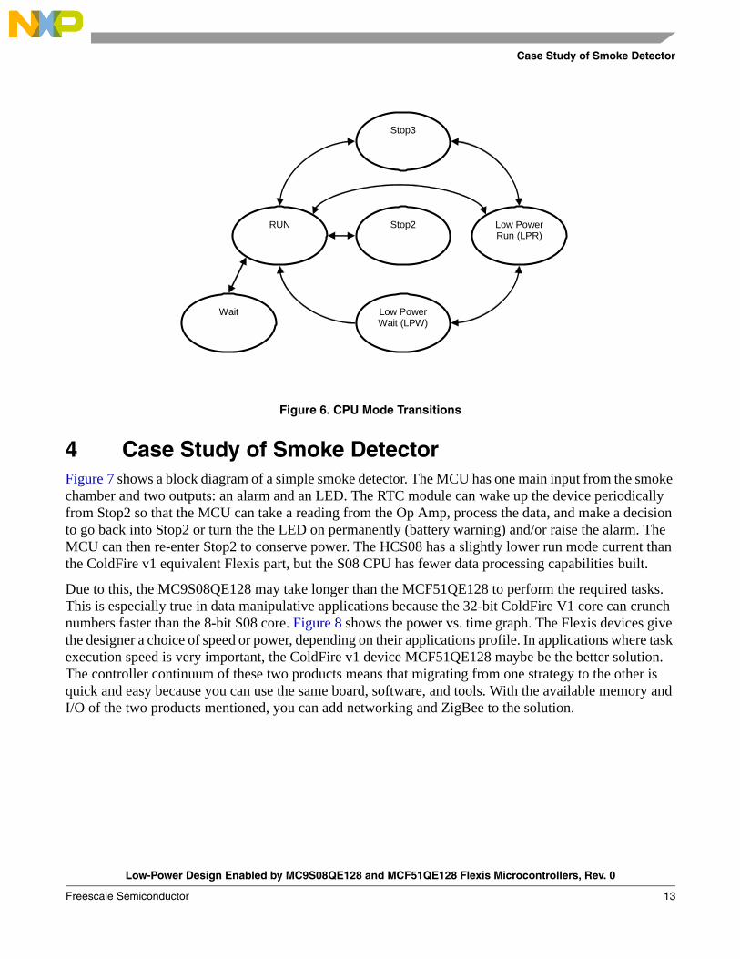
3.3 CPU ModesChoosing the right CPU mode for the right stage of the system design can make or break the products power consumption targets. Exit paths, wake up times and register retention are all parameters that help to choose the most suitable mode. Along with the usual Run mode, the QE128 has five other power saving modes.
3.3.1 Wait Mode
In Wait mode, the CPU shuts down to conserve power. The MCU’s system clocks and full voltage regulation are maintained, saving more power than when the system is in Run mode. Wait mode benefits from the key feature that any interrupt will allow the mode to be exited.
Wait mode saves 30 to 60% of the run mode current, depending on the bus frequency. The higher the frequency, the higher the savings.
The S08 has an indigenous WAIT instruction; however, the ColdFire v1 CPU does not have a WAIT instruction and therefore cannot differentiate between STOP and WAIT modes. The difference between the two is at the device level. The SOPT register has two bits that control the effect of a STOP instruction on the MCF51QE128, STOPE and WAITE.
The STOPE write-once bit enables Stop mode.
The WAITE write-any time bit is used to enable Wait mode.
Low-Power Design Enabled by MC9S08QE128 and MCF51QE128 Flexis Microcontrollers, Rev. 0
Freescale Semiconductor10
Clock Selection
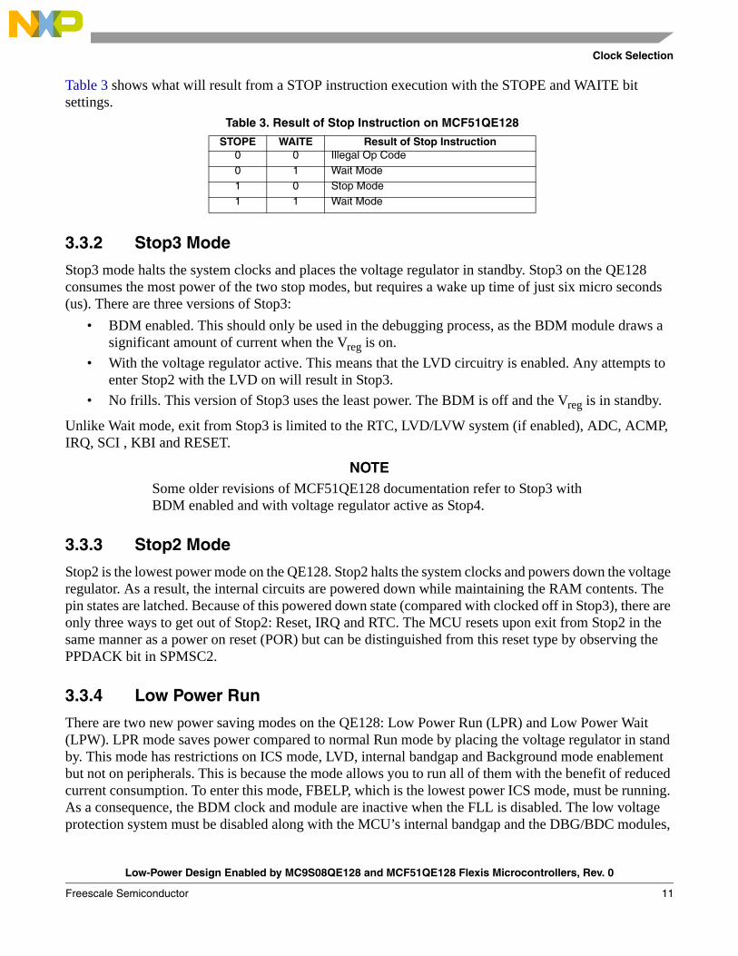
Table 3 shows what will result from a STOP instruction execution with the STOPE and WAITE bit settings.
3.3.2 Stop3 Mode
Stop3 mode halts the system clocks and places the voltage regulator in standby. Stop3 on the QE128 consumes the most power of the two stop modes, but requires a wake up time of just six micro seconds (us). There are three versions of Stop3:
• BDM enabled. This should only be used in the debugging process, as the BDM module draws a significant amount of current when the Vreg is on.
• With the voltage regulator active. This means that the LVD circuitry is enabled. Any attempts to enter Stop2 with the LVD on will result in Stop3.
• No frills. This version of Stop3 uses the least power. The BDM is off and the Vreg is in standby.
Unlike Wait mode, exit from Stop3 is limited to the RTC, LVD/LVW system (if enabled), ADC, ACMP, IRQ, SCI , KBI and RESET.
NOTESome older revisions of MCF51QE128 documentation refer to Stop3 with BDM enabled and with voltage regulator active as Stop4.
3.3.3 Stop2 Mode
Stop2 is the lowest power mode on the QE128. Stop2 halts the system clocks and powers down the voltage regulator. As a result, the internal circuits are powered down while maintaining the RAM contents. The pin states are latched. Because of this powered down state (compared with clocked off in Stop3), there are only three ways to get out of Stop2: Reset, IRQ and RTC. The MCU resets upon exit from Stop2 in the same manner as a power on reset (POR) but can be distinguished from this reset type by observing the PPDACK bit in SPMSC2.
3.3.4 Low Power Run
There are two new power saving modes on the QE128: Low Power Run (LPR) and Low Power Wait (LPW). LPR mode saves power compared to normal Run mode by placing the voltage regulator in stand by. This mode has restrictions on ICS mode, LVD, internal bandgap and Background mode enablement but not on peripherals. This is because the mode allows you to run all of them with the benefit of reduced current consumption. To enter this mode, FBELP, which is the lowest power ICS mode, must be running. As a consequence, the BDM clock and module are inactive when the FLL is disabled. The low voltage protection system must be disabled along with the MCU’s internal bandgap and the DBG/BDC modules,
Table 3. Result of Stop Instruction on MCF51QE128
STOPE WAITE Result of Stop Instruction0 0 Illegal Op Code0 1 Wait Mode1 0 Stop Mode1 1 Wait Mode
Low-Power Design Enabled by MC9S08QE128 and MCF51QE128 Flexis Microcontrollers, Rev. 0
Freescale Semiconductor 11

Clock Selection
it
Ru
LP
W
LP
St
St
as all three consume significant amounts of power regardless of the bus frequency. In addition, Stop2 cannot be entered directly from LPR mode. Because the voltage regulator is in standby, you should keep the power down in this mode.
3.3.5 Low Power Wait
You can only enter Low Power Wait (LPW) mode from LPR mode. As such, the restrictions on LVD circuitry, debugging, and ICS mode are the same. The MCU can typically save 50% of its current consumption in LPW vs. LPR.
3.3.6 CPU Modes Summary
3.3.6.1 S08 and ColdFire v1 Comparison
Table 4 compares the key characteristics of the S08 and Coldfire v1 CPU operation modes. Figure 6 shows what modes transitions are legal.
Table 4. CPU Mode Comparisons
Typical Bus Frequency
Set UpMC9S08QE128
Typical IddMCF51QE128
Typical IddExit Sources
MC9S08QE128 Exit Time
MCF51QE128 ExTime
n 8 MHz FEI mode, running from Flash. All peripherals off and clocks disabled.
6.5 mA 13.2 mA n/a n/a n/a
Run 16 kHz FBELP, running from Flash.All peripherals off and clocks disabled.
22 μA 50 μA Clear LP bit or interrupt with LPWUI set
n/a n/a
ait 8 MHz FEI, entering from Flash. All peripherals off and clocks disabled.
1.8 mA 1.8 mA any interrupt Instantly Instantly
Wait 16 kHz FBELP, entering from Flash.All peripherals off and clocks disabled.
3.3 μA 3.3 μA any interrupt Instantly Instantly
op3 n/a LPO disabled 450 nA 520 nA RTC, LVD/LVW, ADC, ACMP, IRQ,
SCI, KBI, or RESET
6 us 6 us
op2 n/a LPO disabled 350 nA 350 nA RTC, IRQ, or RESET
29 us 29 us
Low-Power Design Enabled by MC9S08QE128 and MCF51QE128 Flexis Microcontrollers, Rev. 0
Freescale Semiconductor12
Case Study of Smoke Detector
Figure 6. CPU Mode Transitions
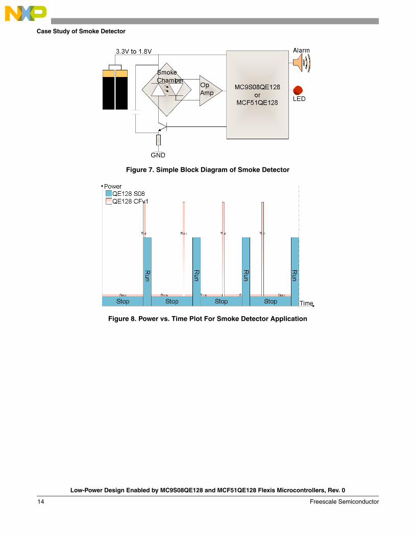
4 Case Study of Smoke DetectorFigure 7 shows a block diagram of a simple smoke detector. The MCU has one main input from the smoke chamber and two outputs: an alarm and an LED. The RTC module can wake up the device periodically from Stop2 so that the MCU can take a reading from the Op Amp, process the data, and make a decision to go back into Stop2 or turn the the LED on permanently (battery warning) and/or raise the alarm. The MCU can then re-enter Stop2 to conserve power. The HCS08 has a slightly lower run mode current than the ColdFire v1 equivalent Flexis part, but the S08 CPU has fewer data processing capabilities built.
Due to this, the MC9S08QE128 may take longer than the MCF51QE128 to perform the required tasks. This is especially true in data manipulative applications because the 32-bit ColdFire V1 core can crunch numbers faster than the 8-bit S08 core. Figure 8 shows the power vs. time graph. The Flexis devices give the designer a choice of speed or power, depending on their applications profile. In applications where task execution speed is very important, the ColdFire v1 device MCF51QE128 maybe be the better solution. The controller continuum of these two products means that migrating from one strategy to the other is quick and easy because you can use the same board, software, and tools. With the available memory and I/O of the two products mentioned, you can add networking and ZigBee to the solution.
Low Power Wait (LPW)
RUN Low Power Run (LPR)
Stop3
Stop2
Wait
Low-Power Design Enabled by MC9S08QE128 and MCF51QE128 Flexis Microcontrollers, Rev. 0
Freescale Semiconductor 13
Case Study of Smoke Detector
Figure 7. Simple Block Diagram of Smoke Detector
Figure 8. Power vs. Time Plot For Smoke Detector Application
Low-Power Design Enabled by MC9S08QE128 and MCF51QE128 Flexis Microcontrollers, Rev. 0
Freescale Semiconductor14
Other MCU Features to Help Save Power
5 Other MCU Features to Help Save Power
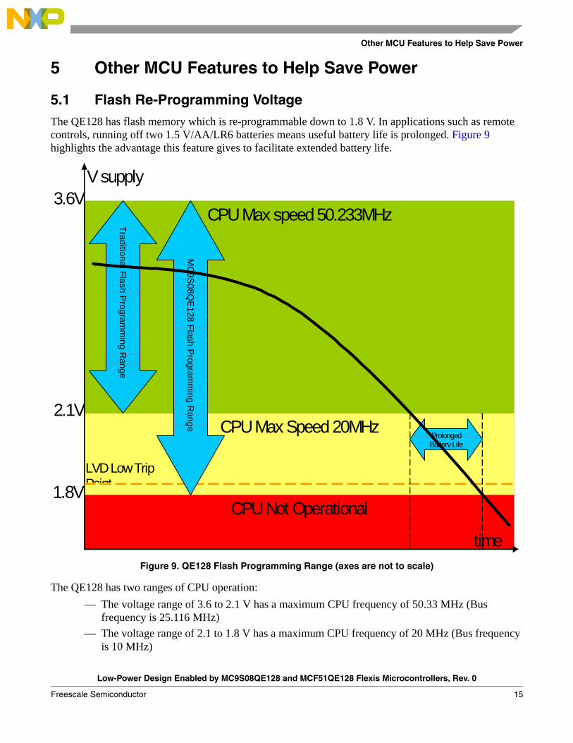
5.1 Flash Re-Programming VoltageThe QE128 has flash memory which is re-programmable down to 1.8 V. In applications such as remote controls, running off two 1.5 V/AA/LR6 batteries means useful battery life is prolonged. Figure 9 highlights the advantage this feature gives to facilitate extended battery life.
Figure 9. QE128 Flash Programming Range (axes are not to scale)
The QE128 has two ranges of CPU operation:— The voltage range of 3.6 to 2.1 V has a maximum CPU frequency of 50.33 MHz (Bus
frequency is 25.116 MHz)— The voltage range of 2.1 to 1.8 V has a maximum CPU frequency of 20 MHz (Bus frequency
is 10 MHz)
CPU Not Operational
CPU Max Speed 20MHz
CPU Max speed 50.233MHz
1.8V
3.6V
2.1V
time
V supply
LVD Low Trip Point
Traditional Flash Program
ming R
ange
MC
9S08Q
E128 Flash P
rogramm
ing Range
Prolonged Battery Life
Low-Power Design Enabled by MC9S08QE128 and MCF51QE128 Flexis Microcontrollers, Rev. 0
Freescale Semiconductor 15
Conclusion
Should an application require that you write to flash to store data (e.g using the flash array to emulate EEPROM), the QE128 will allow the battery life to be extended.
The Low Voltage Detect System (LVD) has a low trip point of 1.84 V. The LVD system is enabled after reset. The POR reset condition of the LVD bit in the System Power Management Status and Control Register 3 (SPMSC3) is zero, which means the LVD circuit will hold the device in reset while the supply is still below 1.84 V. The exception is a wake up from Stop2, which leaves the LVD system setting unchanged. This means that if an application is intended to run down to 1.80 V, resets should be avoided as the only way to recover would be to change the batteries.
5.2 Port Manipulation
5.2.1 Slew Rate Control
All of the device’s output pins have slew rate control which, when driving external components, can reduce power by slowing transients.
5.2.2 Drive Strength Control
Each GPIO pin can operate at either high or low drive strength. If high strength is selected, the pin sources or sinks higher currents. This means that the MCU consume more power. Low drive strength with a small loading on the pins keeps the power consumption of the MCU and the application at a minimum.
5.2.3 Unused Pins
All unused pins in the application (including, on smaller packages, the GPIO which are not bonded out to the pins) should be pulled up by the internal pull up resistor (PTxPE) if they are set up as inputs, or if they should be set up as outputs driving low to keep power consumption down and to improve the application robustness.
6 ConclusionBy giving careful consideration to the clock source, clock distribution and clock mode on a module basis, and using the correct CPU mode at the right time and for the right length of time, the tight power consumption limits placed on modern consumer and industrial products can be achieved using the QE128. However, the clocks and CPU modes are not the only power-reducing features. There are also other, simpler features such as slew rate and port manipulation (as described previously).
A careless design would at least double the power consumption of the system. The features incorporated in the QE128 are simple. The diversity of the new features means that they benefit all types of applications whether or not the battery remains powered. They are easy to understand, incorporate and use, allowing system designers to use them to decrease the system’s overall power consumption.
Low-Power Design Enabled by MC9S08QE128 and MCF51QE128 Flexis Microcontrollers, Rev. 0
Freescale Semiconductor16

THIS PAGE IS INTENTIONALLY BLANK
Low-Power Design Enabled by MC9S08QE128 and MCF51QE128 Flexis Microcontrollers, Rev. 0
Freescale Semiconductor 17

Document Number: AN3460Rev. 006/2007
How to Reach Us:
Home Page:www.freescale.com
Web Support:http://www.freescale.com/support
USA/Europe or Locations Not Listed:Freescale Semiconductor, Inc.Technical Information Center, EL5162100 East Elliot RoadTempe, Arizona 85284+1-800-521-6274 or +1-480-768-2130www.freescale.com/support
Europe, Middle East, and Africa:Freescale Halbleiter Deutschland GmbHTechnical Information CenterSchatzbogen 781829 Muenchen, Germany+44 1296 380 456 (English)+46 8 52200080 (English)+49 89 92103 559 (German)+33 1 69 35 48 48 (French)www.freescale.com/support
Japan:Freescale Semiconductor Japan Ltd.HeadquartersARCO Tower 15F1-8-1, Shimo-Meguro, Meguro-ku,Tokyo 153-0064Japan0120 191014 or +81 3 5437 [email protected]
Asia/Pacific:Freescale Semiconductor Hong Kong Ltd.Technical Information Center2 Dai King StreetTai Po Industrial EstateTai Po, N.T., Hong Kong+800 2666 [email protected]
For Literature Requests Only:Freescale Semiconductor Literature Distribution CenterP.O. Box 5405Denver, Colorado 802171-800-441-2447 or 303-675-2140Fax: [email protected]
Information in this document is provided solely to enable system and software implementers to use Freescale Semiconductor products. There are no express or implied copyright licenses granted hereunder to design or fabricate any integrated circuits or integrated circuits based on the information in this document.
Freescale Semiconductor reserves the right to make changes without further notice to any products herein. Freescale Semiconductor makes no warranty, representation or guarantee regarding the suitability of its products for any particular purpose, nor does Freescale Semiconductor assume any liability arising out of the application or use of any product or circuit, and specifically disclaims any and all liability, including without limitation consequential or incidental damages. “Typical” parameters that may be provided in Freescale Semiconductor data sheets and/or specifications can and do vary in different applications and actual performance may vary over time. All operating parameters, including “Typicals”, must be validated for each customer application by customer’s technical experts. Freescale Semiconductor does not convey any license under its patent rights nor the rights of others. Freescale Semiconductor products are not designed, intended, or authorized for use as components in systems intended for surgical implant into the body, or other applications intended to support or sustain life, or for any other application in which the failure of the Freescale Semiconductor product could create a situation where personal injury or death may occur. Should Buyer purchase or use Freescale Semiconductor products for any such unintended or unauthorized application, Buyer shall indemnify and hold Freescale Semiconductor and its officers, employees, subsidiaries, affiliates, and distributors harmless against all claims, costs, damages, and expenses, and reasonable attorney fees arising out of, directly or indirectly, any claim of personal injury or death associated with such unintended or unauthorized use, even if such claim alleges that Freescale Semiconductor was negligent regarding the design or manufacture of the part.
RoHS-compliant and/or Pb-free versions of Freescale products have the functionality and electrical characteristics as their non-RoHS-compliant and/or non-Pb-free counterparts. For further information, see http://www.freescale.com or contact your Freescale sales representative.
For information on Freescale’s Environmental Products program, go to http://www.freescale.com/epp.
Freescale™ and the Freescale logo are trademarks of Freescale Semiconductor, Inc. All other product or service names are the property of their respective owners.© Freescale Semiconductor, Inc. 2007. All rights reserved.