low noise mix-mode integrated circuits for …†“nsw↑t c h workshop „spin momentum...
TRANSCRIPT
S P↓N S W↑T C H Workshop „Spin Momentum Transfer” , Kraków 2008
Low Noise Mix-Mode Integrated Circuits for Micro-sensor readout
Paweł GrybośDepartment of Measurement and Instrumentation
AGH University of Science and Technology

S P↓N S W↑T C H Workshop „Spin Momentum Transfer” , Kraków 2008
1. Introduction: multichannel low noise integrated circuit
2. Noise, crostalk and matching
3. Digital imaging system for diffractometry applications
4. Multichannel neurobiology experiments
5. Conclusions
Outline
S P↓N S W↑T C H Workshop „Spin Momentum Transfer” , Kraków 2008
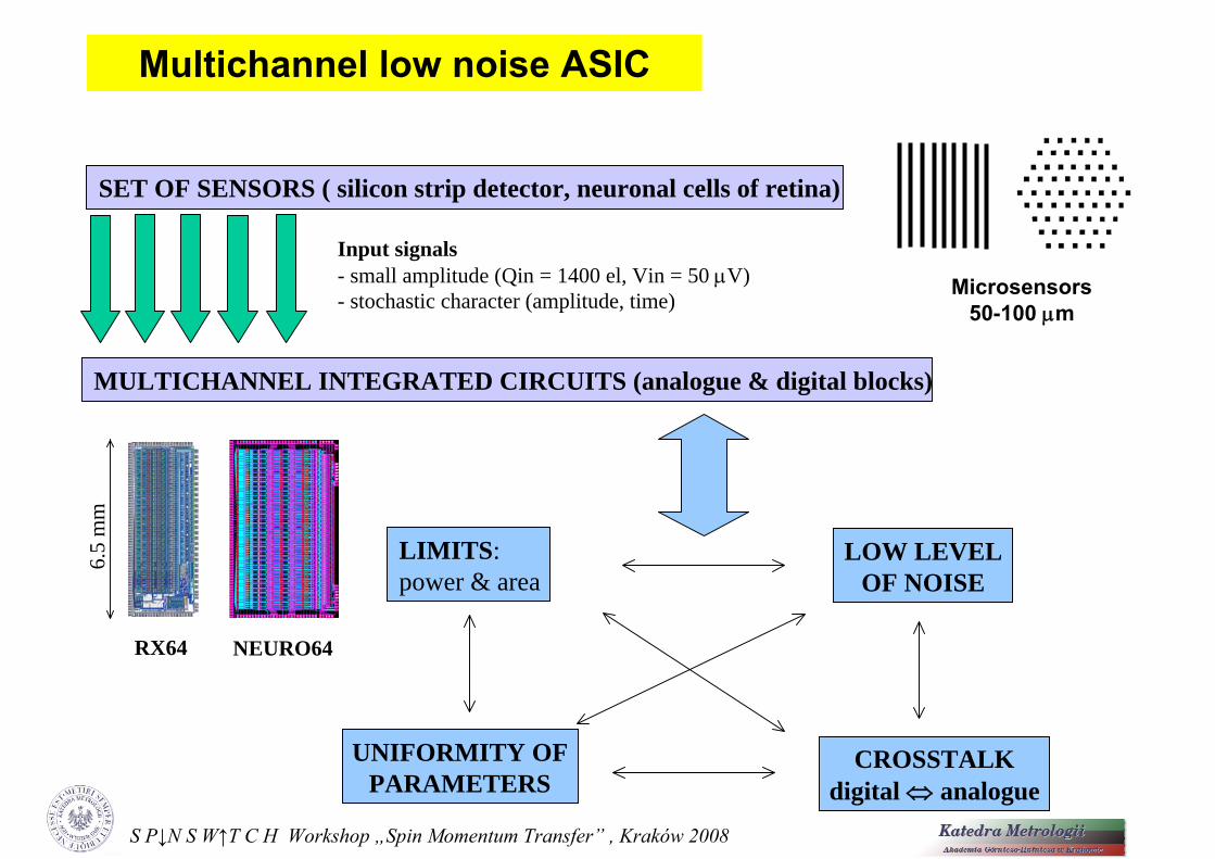
Multichannel low noise ASIC
Input signals- small amplitude (Qin = 1400 el, Vin = 50 μV)- stochastic character (amplitude, time)
SET OF SENSORS ( silicon strip detector, neuronal cells of retina)
MULTICHANNEL INTEGRATED CIRCUITS (analogue & digital blocks)
CROSSTALKdigital ⇔ analogue
LIMITS: power & area
LOW LEVELOF NOISE
UNIFORMITY OFPARAMETERS
6.5
mm
RX64 NEURO64
Microsensors50-100 μm

S P↓N S W↑T C H Workshop „Spin Momentum Transfer” , Kraków 2008
Noise in MOS transistors
mth kTg
dfdi
382
=
saturation
dsth kTg
dfdi 4
2
=
linear
Simulations (HSPICE) NLEV=3 ( ) GDSNIO
aaaVV
LWCkT
dfdi
TGSoxth
+++
−=1
13
8 22
μ
BSIM3v3 (NIMOD=2) inveff
effth QL
kTdfdi
2
2 4 μ=
1. Thermal noise of channel
Measurments – short channel effects (2-10x):( velocity saturation, hot electrons)
2. Flicker noise
Simulations (HSPICE)
NLEV=2, 3 AFeffeff
m
ox
f
fLWg
CKF
dfdi 122
/1 =
Measurments – short channel effects( hot electrons, RST noise)
BSIM3v3 (NIMOD=2)
Time
V(t)
Signal Signal+noise
S P↓N S W↑T C H Workshop „Spin Momentum Transfer” , Kraków 2008
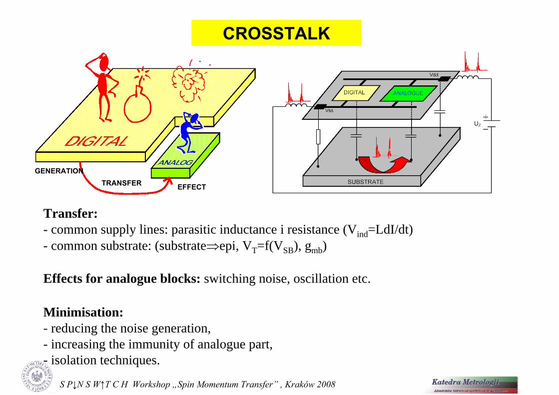
CROSSTALK
Transfer:- common supply lines: parasitic inductance i resistance (Vind=LdI/dt)- common substrate: (substrate⇒epi, VT=f(VSB), gmb)
Effects for analogue blocks: switching noise, oscillation etc.
Minimisation:- reducing the noise generation,- increasing the immunity of analogue part,- isolation techniques.
GENERATIONTRANSFER EFFECT

S P↓N S W↑T C H Workshop „Spin Momentum Transfer” , Kraków 2008
RANDOM MATCHING
( ) 222
2 DSWLAP P
P +=Δσ
For MOS transistors: VT0 , β, γ
ox
BFs
ox
oxFMST0 C
NqCQV
φεφφ
42 +−+=
LWCoxμβ =
ox
Bs
CNqε
γ2
=
CMOS 0.7μm - σ(VT0) NMOS PMOS
W/L=2μm/0.7μm 9.72 mV 19.43 mV
W/L=1500μm/1.5μm 0.31 mV 0.63 mV
L
W
L
W
D
MATCHING - identically design devices have different parameters ΔP=P1-P2 (ΔP/P)

S P↓N S W↑T C H Workshop „Spin Momentum Transfer” , Kraków 2008
Two Examples of Low Noise Mix-Mode Integrated Circuits
Diffractometry Neurobiology

S P↓N S W↑T C H Workshop „Spin Momentum Transfer” , Kraków 2008
Digital X-ray Imaging System
Digital Imaging System(X-rays photon counting)
Position sensitive systemwith a good spatial resolution
High dynamic range &relatively high X-ray intensity
Energy window selectionfor X-ray photons
MULTICHANNELSYSTEM
+ ARRAY OF SENSORDISCRIMINATORS
SHORT TIME OFPULSE PROCESSING
Applications:- clinical diagnostic: dual energy mammography & angiography- material science - diffractometry

S P↓N S W↑T C H Workshop „Spin Momentum Transfer” , Kraków 2008
Scheme of imaging system
Silicon strip detector⇓
• good spatial resolution: tens of μm
• energy resolution: 3.67 eV/e-h
• single photon counting mode
• good efficiency
Multichannel ASIC(analog processing + data storage)
⇓
• binary readout architecture to cope with high X-ray intensity
• selection of pulses according their amplitude
control,data
X- ray

S P↓N S W↑T C H Workshop „Spin Momentum Transfer” , Kraków 2008
Problems with binary readoutfor X-ray applications
Pulse height spectrum
1) Counting pulses N
2) dN/dVTH

S P↓N S W↑T C H Workshop „Spin Momentum Transfer” , Kraków 2008
Multichannel ASIC architecture
DEDIX: Dual Energy Digital X-ray Imaging
S P↓N S W↑T C H Workshop „Spin Momentum Transfer” , Kraków 2008
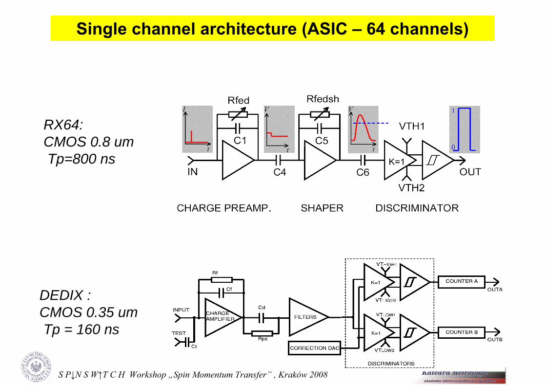
Single channel architecture (ASIC – 64 channels)
RX64:CMOS 0.8 umTp=800 ns
DEDIX :CMOS 0.35 umTp = 160 ns

S P↓N S W↑T C H Workshop „Spin Momentum Transfer” , Kraków 2008
Why correction is necessary?
DC coupling between stages – base line changes from channel to channel
BaseLine
VT HIGH
VT LOW

S P↓N S W↑T C H Workshop „Spin Momentum Transfer” , Kraków 2008
Spectrum of X-ray source – measurement set-up
Pu-238 source
Cu (Fe, Zn) foil
Si strip detector DEDIX
Serial output
13.6; 17.2; 20.1 keV
8.04keV
eleV
keVQ
eleV
keVQ
eleV
keVQ
eleV
keVQ
547667.31.20
468667.32.17
370567.36.13
219067.3
04.8
4
3
2
1
==
==
==
==
S P↓N S W↑T C H Workshop „Spin Momentum Transfer” , Kraków 2008
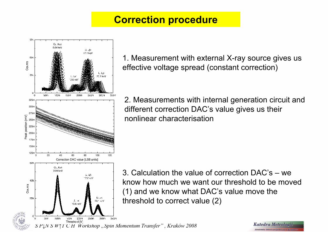
Correction procedure
1. Measurement with external X-ray source gives useffective voltage spread (constant correction)
2. Measurements with internal generation circuit anddifferent correction DAC’s value gives us theirnonlinear characterisation
3. Calculation the value of correction DAC’s – we know how much we want our threshold to be moved(1) and we know what DAC’s value move thethreshold to correct value (2)

S P↓N S W↑T C H Workshop „Spin Momentum Transfer” , Kraków 2008
High count-rate measurement with X-ray tube
S P↓N S W↑T C H Workshop „Spin Momentum Transfer” , Kraków 2008
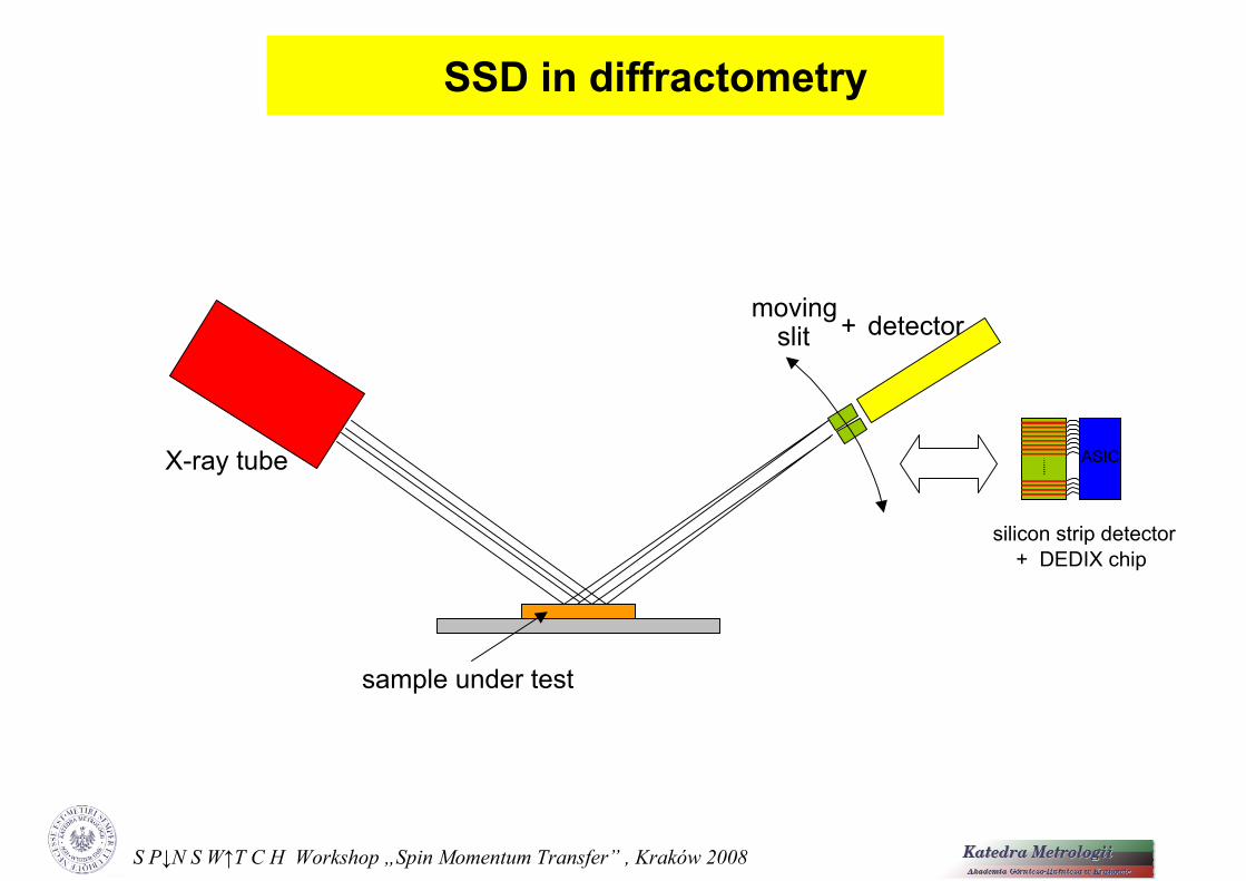
SSD in diffractometry
X-ray tube
+ detectormoving
slit
sample under test
ASIC
silicon strip detector+ DEDIX chip
S P↓N S W↑T C H Workshop „Spin Momentum Transfer” , Kraków 2008
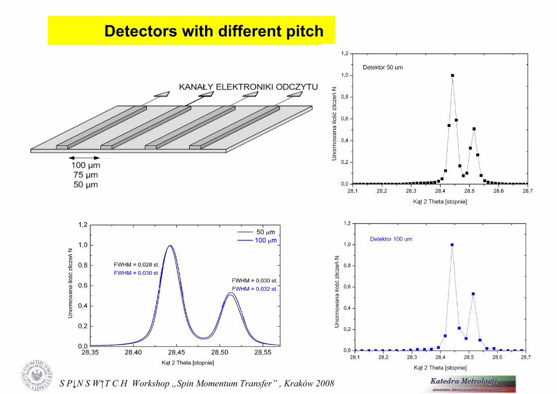
Detectors with different pitch

S P↓N S W↑T C H Workshop „Spin Momentum Transfer” , Kraków 2008
Continous scan (prof. T. Stobiecki laboratory)
S P↓N S W↑T C H Workshop „Spin Momentum Transfer” , Kraków 2008
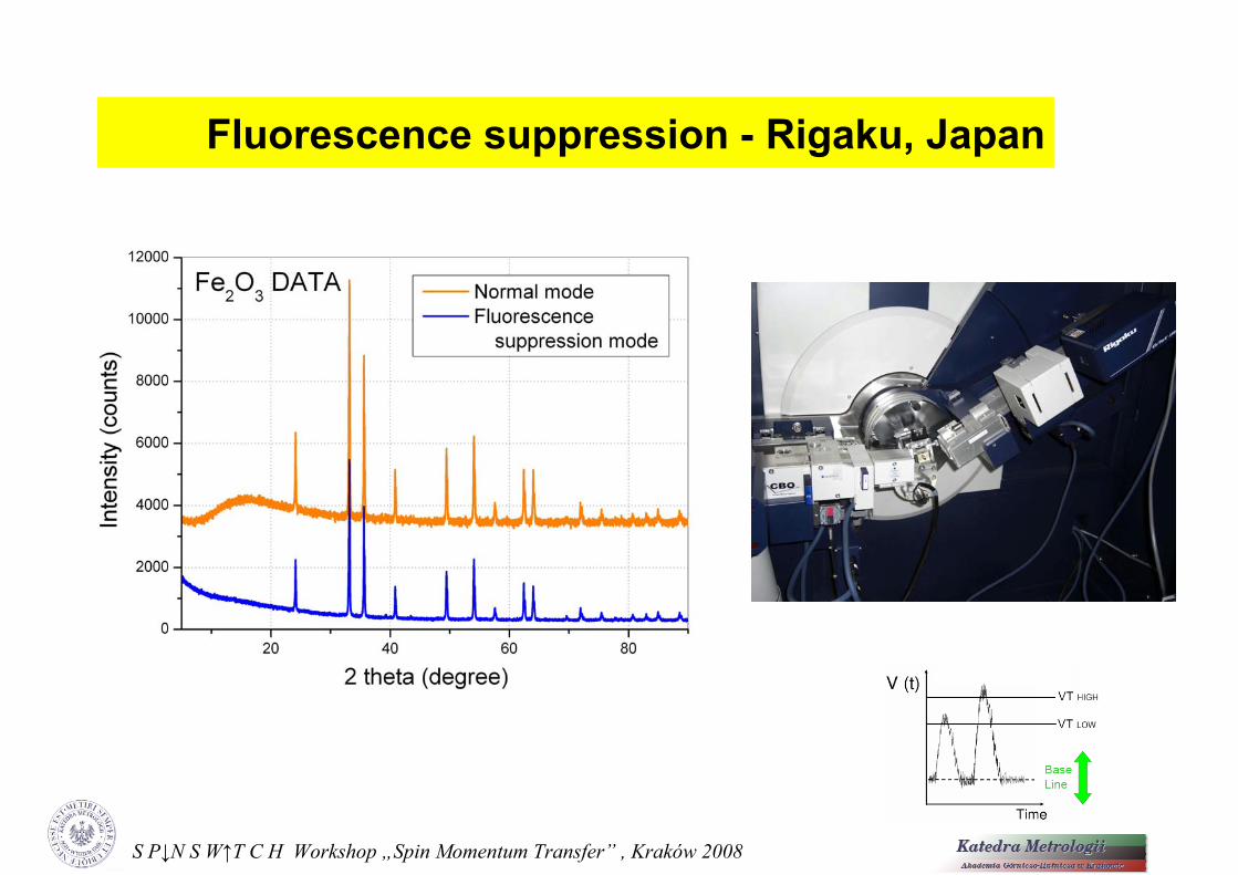
Fluorescence suppression - Rigaku, Japan

S P↓N S W↑T C H Workshop „Spin Momentum Transfer” , Kraków 2008
CCD detector
S P↓N S W↑T C H Workshop „Spin Momentum Transfer” , Kraków 2008
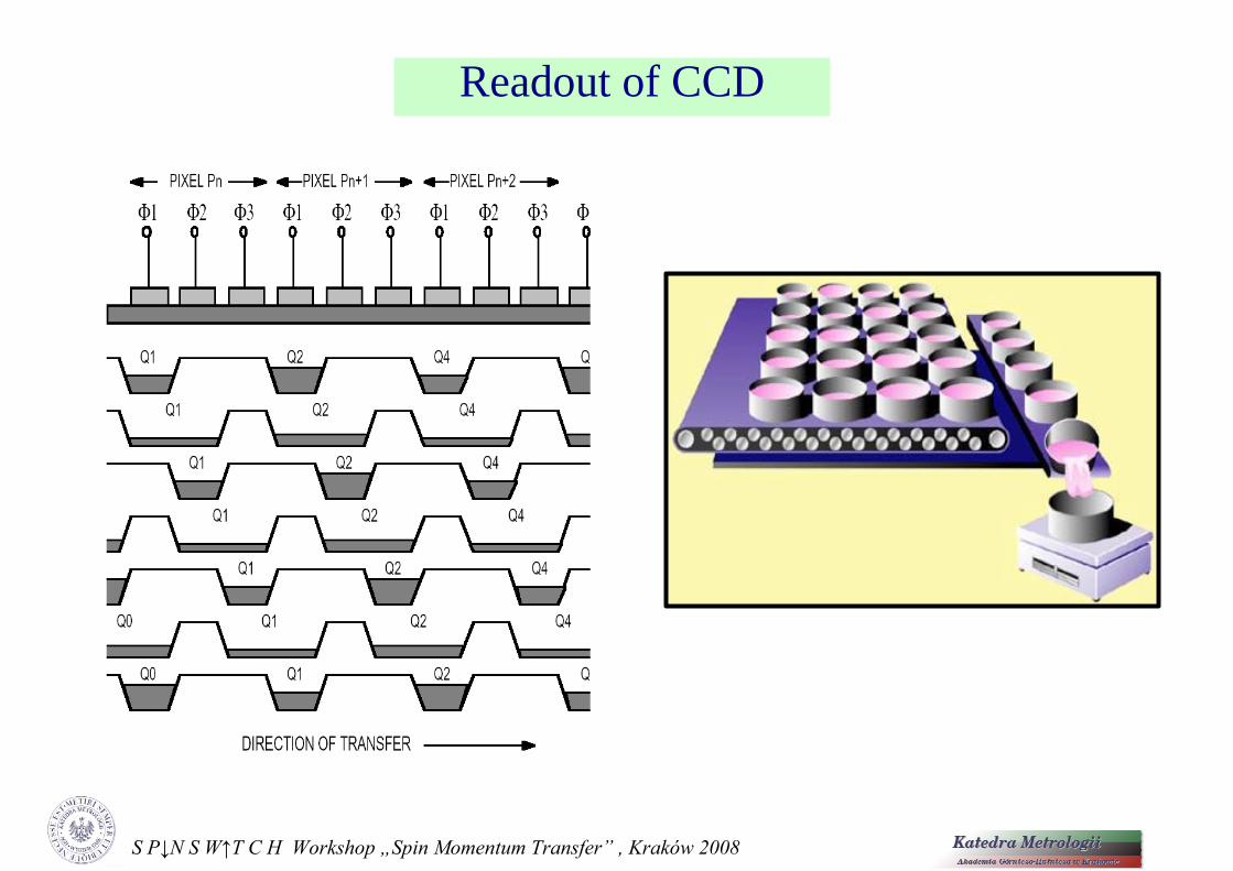
Readout of CCD

S P↓N S W↑T C H Workshop „Spin Momentum Transfer” , Kraków 2008
Pixel detector Si/GaAs
Picture: CERN

S P↓N S W↑T C H Workshop „Spin Momentum Transfer” , Kraków 2008
Bump Bonding

S P↓N S W↑T C H Workshop „Spin Momentum Transfer” , Kraków 2008
Medipix -CERN

S P↓N S W↑T C H Workshop „Spin Momentum Transfer” , Kraków 2008
Medipix -CERN

S P↓N S W↑T C H Workshop „Spin Momentum Transfer” , Kraków 2008
Medipix -CERN

S P↓N S W↑T C H Workshop „Spin Momentum Transfer” , Kraków 2008
Medipix -CERN

S P↓N S W↑T C H Workshop „Spin Momentum Transfer” , Kraków 2008
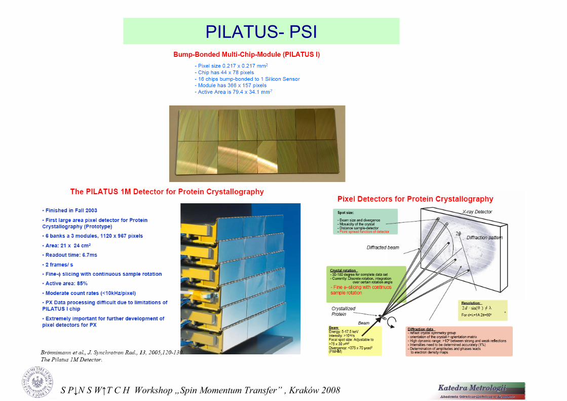
PILATUS - PSI
S P↓N S W↑T C H Workshop „Spin Momentum Transfer” , Kraków 2008
PILATUS- PSI

S P↓N S W↑T C H Workshop „Spin Momentum Transfer” , Kraków 2008
Low Noise Mix-Mode Integrated Circuits for Neurobiology Applications

S P↓N S W↑T C H Workshop „Spin Momentum Transfer” , Kraków 2008
History – single channel recording
‘Patch-clamp’ technique : Neher & Sakmann, 1976, (Nobel Prize1991)

S P↓N S W↑T C H Workshop „Spin Momentum Transfer” , Kraków 2008
Neural systems
BRAIN
RETINA
Cones: 6.5 x 10⁶ (colours)Rods: 125 x 106 (move, shape)Optical nerve: 1 x 10⁶ fibers
Photo: Biologia, PWN
Single neuron

S P↓N S W↑T C H Workshop „Spin Momentum Transfer” , Kraków 2008
Motivation
1.Understand neuronal coding,
2. Biosensors
3. Neuronal prostheses
for recording/stimulation of neuronal system comprising several hundreds or thousands of electrodes
AIM: to build an electronic interface
Components
1.Microelectrode array
2. Multichannel electronics

S P↓N S W↑T C H Workshop „Spin Momentum Transfer” , Kraków 2008
Microelectrode arrays I – planar microelectrodes
Ayanda Biosystems
Multi Channel SystemsUniversity of Glasgow
512-electrode array 32x16: spacing = 60 um diameter = 5 um

S P↓N S W↑T C H Workshop „Spin Momentum Transfer” , Kraków 2008
Microelectrode arrays II - Microprobes
NeuroNexus Technologies
Utah Microelectrode Array

S P↓N S W↑T C H Workshop „Spin Momentum Transfer” , Kraków 2008
Recording/stimulation electronics – standart solutions
60-channel recording system
8-channel stimulus generator
4-channel recording amplifier
Limits:
- number of channels
- large volume and weight
- high costs
S P↓N S W↑T C H Workshop „Spin Momentum Transfer” , Kraków 2008
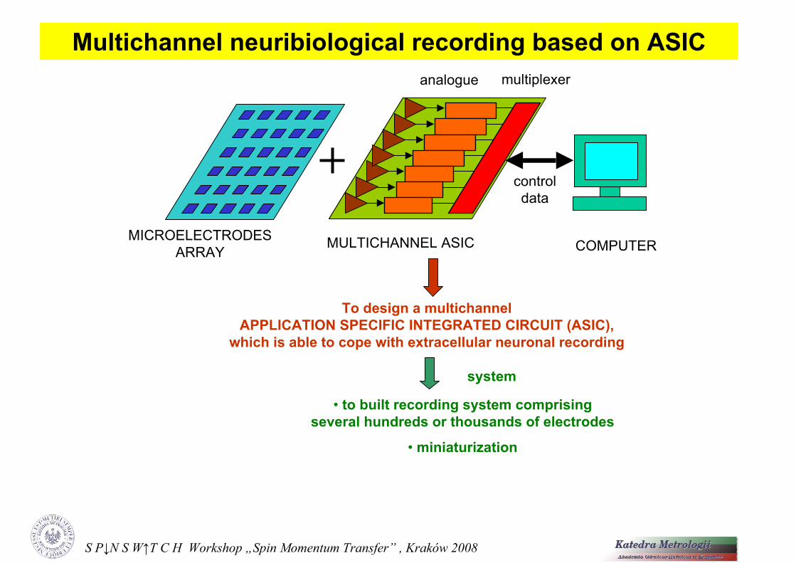
Multichannel neuribiological recording based on ASIC
MICROELECTRODES ARRAY
analogue multiplexer
control data
MULTICHANNEL ASIC COMPUTER
To design a multichannelAPPLICATION SPECIFIC INTEGRATED CIRCUIT (ASIC),
which is able to cope with extracellular neuronal recording
• to built recording system comprising several hundreds or thousands of electrodes
• miniaturization
system

S P↓N S W↑T C H Workshop „Spin Momentum Transfer” , Kraków 2008
Extracellular recording – requirements for electronics
Requirements:
Low noise ~ 5 μV rms Frequency band pass 20 Hz to 2000 HzAC coupled input cut-off frequency < 20 Hz
Signal source (e.g. retina tissue): Vamp = 50-500 μV, DC offsets,tw ≈ 1-2 ms, band: 20 -2000 Hz,
MULTICHANNEL ARCHITECTURE

S P↓N S W↑T C H Workshop „Spin Momentum Transfer” , Kraków 2008
Multichannel architecture
LIMITATION OF CMOS TECHNOLOGY
64 channel ASIC - NEURO64 Single channel architecture
CMOS technology 0.7 um4 mm x 6 mm

S P↓N S W↑T C H Workshop „Spin Momentum Transfer” , Kraków 2008
CMOS technology - noise
MOS transistors:- flicker noise ⇐ low frequency,- thermal noise ⇐ power limitation
AC-coupling -kT/C noise:- small capacitors ⇐ area limitationCMOS technology: C= 1pF ⇒ 64μV rms
C= 100pF ⇒ 6.4μV rmsSMD technology: C= 10nF ⇒ 0.64μV rms
Crosstalk:- supply bounce, - substrate noise
R
Creadoutelectrode
S P↓N S W↑T C H Workshop „Spin Momentum Transfer” , Kraków 2008
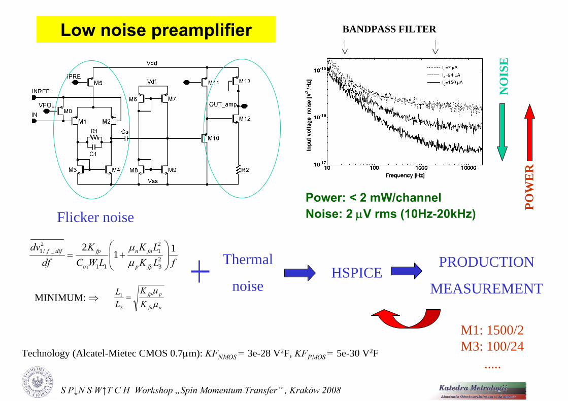
Low noise preamplifier
fLKLK
LWCK
dfdv
fpp
fnn
ox
fpdiff 112
23
21
11
2_/1
⎟⎟⎠
⎞⎜⎜⎝
⎛+=μμ
nfn
pfp
KK
LL
μμ
=3
1
Power: < 2 mW/channelNoise: 2 μV rms (10Hz-20kHz)
Technology (Alcatel-Mietec CMOS 0.7μm): KFNMOS = 3e-28 V2F, KFPMOS = 5e-30 V2F
Flicker noise
NO
ISE
POW
ER
MINIMUM: ⇒
Thermal
noiseHSPICE
PRODUCTION
MEASUREMENT
M1: 1500/2 M3: 100/24
.....
BANDPASS FILTER

S P↓N S W↑T C H Workshop „Spin Momentum Transfer” , Kraków 2008
AC coupling – NEURO64
WEAKINVERSION
STRONGINVERSION
R ⇒ GΩ !
Cs = 4pF
Measurements f=10 mHzSimulations

S P↓N S W↑T C H Workshop „Spin Momentum Transfer” , Kraków 2008
CROSSTALK PROBLEM:analogue multiplexer
(input noise VIN-rms < 5 μV rms)
Multiplexer in NEURO64 ⇒ to reduce crosstalk
Referencechannel

S P↓N S W↑T C H Workshop „Spin Momentum Transfer” , Kraków 2008
Matching
Measure parameters
S P↓N S W↑T C H Workshop „Spin Momentum Transfer” , Kraków 2008
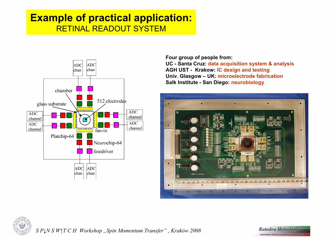
Example of practical application:RETINAL READOUT SYSTEM
Four group of people from:UC - Santa Cruz: data acquisition system & analysisAGH UST - Krakow: IC design and testingUniv. Glasgow – UK: microelectrode fabricationSalk Institute - San Diego: neurobiology

S P↓N S W↑T C H Workshop „Spin Momentum Transfer” , Kraków 2008
Experimental set-upRETINAL READOUT SYSTEM
A movie is focused on the retina tissue
⇓The patterns of electrical activity generated by hundreds of retinal
output neurons are recorded
Experiments have been done in:Salk Institute, San Diegohttp://www.snl-e.salk.edu
Retinal tissue placed on top of mulielectrode array

S P↓N S W↑T C H Workshop „Spin Momentum Transfer” , Kraków 2008
Working system with 512 readout channels
To understand how the retina processes and encodes dynamic visual image
Out
put v
olta
ge [m
V]
Time [ms]
Fragment modułu512-kanałowy
NEURO64
PLAT64
"pitch adaptor"
512 electrodeswith retina tissue

S P↓N S W↑T C H Workshop „Spin Momentum Transfer” , Kraków 2008
Electrodespike-rate
Spike-rate forOn-off DS
neurons
Spike-rate forOn-off DS
neurons
2 mm
Tests with the monkey retina – moving bar(Litke, et. al.)
S P↓N S W↑T C H Workshop „Spin Momentum Transfer” , Kraków 2008
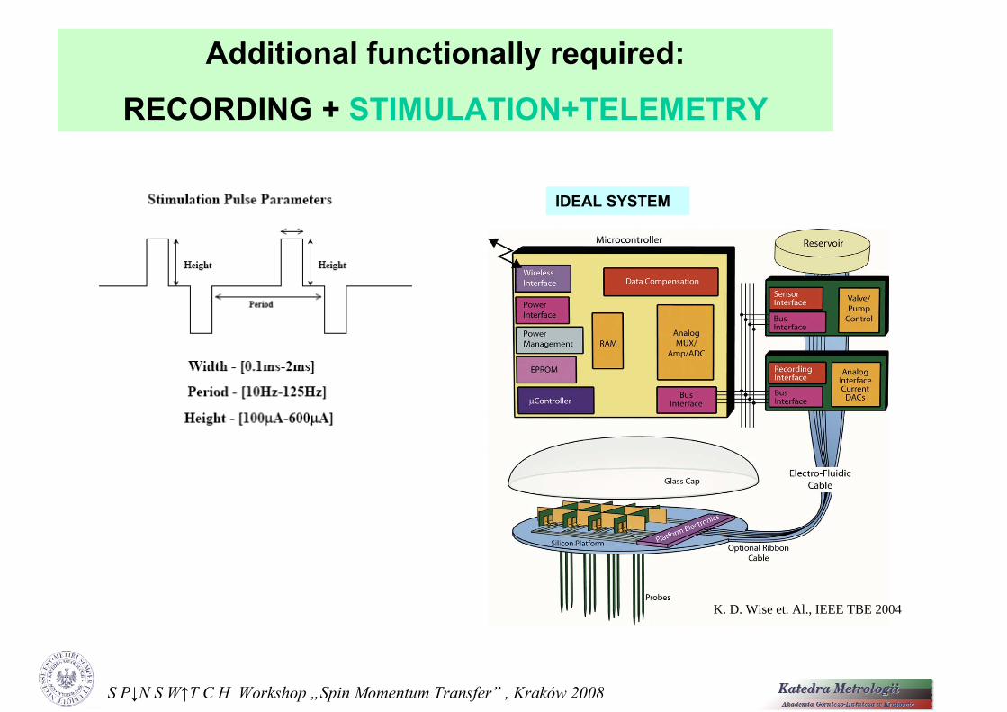
Additional functionally required:
RECORDING + STIMULATION+TELEMETRY
K. D. Wise et. Al., IEEE TBE 2004
IDEAL SYSTEM

S P↓N S W↑T C H Workshop „Spin Momentum Transfer” , Kraków 2008
RP - RetinisPigmentosa
( 12 mln people)
Effect of Effect of RetinaRetina DiseasesDiseases..
Normal Macular Degeneration (AMD)

S P↓N S W↑T C H Workshop „Spin Momentum Transfer” , Kraków 2008
System MIT/Harvard(epiretinal implant)
Optiobionics Corporation(subretinal implant)
ASR: 2 mm x 25 um5000 pixels,: 20 um x 20 um

S P↓N S W↑T C H Workshop „Spin Momentum Transfer” , Kraków 2008
NeuroNexus Technologies
Deep brain stimulation – microprobes
Next step - MEMS

S P↓N S W↑T C H Workshop „Spin Momentum Transfer” , Kraków 2008
Summary