logi-bone user guide - farnell element14 | electronic ... · logi-bone user guide ... hizrp_sda...
TRANSCRIPT

Logi-Bone User Guide
From ValentFx Wiki
LOGi-Bone - User Guide
Bringing FPGA Technology to the Beaglebone
Contents
1 Overview
1.1 Features1.2 Peripherals
2 Electrical
3 Interfacing3.1 LOGi-Bone Board Component Identification
3.2 BeagleBone P8/P9 Connector Pin Usage3.3 LOGi-Bone Shared Pin Functions3.4 BeagleBone EMMC - GPMC - HDMI Functionality
3.4.1 BBB Peripheral Priorities in the LOGi-Bone Design3.4.2 EMMC with the LOGi-Bone / BBB
3.5 PMOD Expansion Port3.6 Arduino Expansion Port3.7 ADC Functionality and Wiring3.8 SATA Expansion Port3.9 LVDS signal usage
3.10 Push Button Usage3.11 DIP Switch Usage3.12 LED Usage
3.13 JTAG Interface4 Device Tree requirements
4.1 Kickstarter Early Bird Boards auto device-tree setup4.2 Example Device-Tree overlays and scripts
5 LOGi-bone template driver
5.1 Compiling the template driver5.1.1 Installing a the toolchain
5.1.2 Installing the kernel source5.1.3 Installing and compiling logibone template driver
5.2 Creating your own template driver6 Programming the FPGA from the Beaglebone
6.1 Manually installing the LOGi-Loader
6.2 Process for running the LOGi-Loader:7 BeagleBone to FPGA Interfaces
7.1 BBB GPMC to FPGA Interface7.1.1 Current GPMC performance with the LOGI Drivers
7.2 LOGI GPMC driver implementation details
8 Useful Links
8.1 Logi - Repository - Projects, Libraries, Drivers8.2 Logi-Bone Schematics
8.3 Logi-Bone User Guide -Logi-Bone documentation
8.4 Logi Projects wiki - LOGI and Users projects will be documented here
Overview
The LOGi-Bone is the first FPGA development platform that has been optimized for use with the Beaglebone. TheLOGi-Bone adds FPGA flexibility and capability that allows the Beaglebone to be easily morphed into a myriadof digital applications. The FPGA/CPU combination the LOGi- creates an incredibly powerful and versatile digitalcanvas for users to create their imaginative digital designs.
Features
FPGA: Spartan 6 LX9 – TQFP144 Package - XC6SLX9-2TQG144C
Plug and play interfacing the Beaglebone
Arduino Shield expansion allowing for more than 200 existing plug in hardware modules
PMOD compatible headers allowing for more than 50 existing low cost hardware modules
4 layer optimized design to support maximum performance of high bandwidth applicationsLength tuned GPMC, SDRAM and LVDS signals for high performance applications
50 Mhz MEMS oscillator
Peripherals
2x Push buttons
2x DIP Switch
1x High bandwidth SATA connector expansion port
32 FPGA IO available through PMOD and Arduino headers
2x Digilent Inc. PMOD ports supporting 59+ plug and play hardware modules1x Arduino Header supporting 200+ Arduino Shield modules
Optional I2C, SPI access from the Beaglebone
10x length matched LVDS pairs routed as: 100 ohm differential, 50 ohm single-ended
256 Mb SDRAM
Electrical
External Vin Connector
Voltage
Max.
Voltage
Nominal
Voltage
Min.
6V 5V 4V
The LOGi-Bone can be powered through the Beaglbone connector or from the on-board external power connector. If powering the LOGi-Bone from the Beaglebone connector, it is recommended that a 1A external power supply beused to power the Beaglebone. Most FPGA applications will not require the use of a separate external powersupply to power the LOGi-Bone, but it is up to to ensure that the FPGA applications will not over-load theBeaglebone power rails which will cause brown-outs and or system failures.
All current LOGi applications can be run while being powered only from the Beaglebone connector. The usershould test newly designed applications to ensure the FPGA load falls within acceptable values. Information relevantto the Beaglebone system power requirements can be found the Beaglebone wiki.
The LOGi-Bone uses LDO regulators to supply 3V3 and 1V2 to the onboard peripherals and the FPGA in order toreduce costs. The power distribution was designed to allow maximum dissipated heat to the internal and externalpower planes. If very high demand applications are designed testing should be done to ensure that the LDOregulators are not overheated due to the heavy loads. All current applications have been tested including the heavyload of the bitcoin mining applications and no over-heating issues have been found.
Interfacing
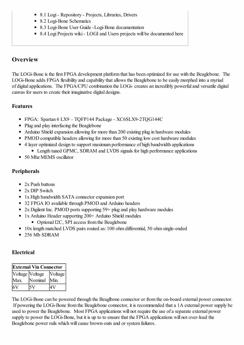
The LOGi-Bone was designed to allow for easyexpansion to a maximum number of off-the-shelf hardwaremodules. The LOGi-Bone uses Digilent Inc. PMOD expansion ports and an Arduino Shield expansion port thatgive users a plug-and-play experience with over 250 off-the-shelf hardware modules. A SATA port was added toboard to be used for maximum bandwidth applications. There are 10 LVDS pairs routed on the board that are alllength matched. These interfaces will allow for a multitude of varying applications to be implemented on the LOGi-Bone. Due to the high amount of flexibility of the board, some pin functions are shared between differentperipherals. This section will cover the details of the peripherals and how to use to while eliminating any pin conflicts.
Top Level Block Diagram
LOGi-Bone Board Component Identification

Figure: LOGi-Bone Top components
1. U5 - Xilinx Spartan 6 - FPGA (XC6SLX9-2TQG144C)
2. U6 - Micron Technology Inc. - 16Mbit Serial Flash (M25PE16)
3. U8 - I/O Expander 8BIT I2C/SMBUS I/O
4. U6 - Abracon Corporation - 50MHz Oscillator (ASDMB-50.000MHZ-LC-T)
5. J2 - Digilent Inc. 5 Pin JTAG Header
6. IC EEPROM 256KBIT 400KHZ
7. 3V3 LDO to supply FPGA IO banks, SDRAM, peripheral IC’s
8. 1V2 LDO for FPGA core voltage
9. SATA connector for high bandwidth module interfaces supporting LVDS
10. Push button 2 (Active low)
11. Push button 1 (Active low) - Can be configured as FPGA hard reset using solder jumper JP1 on bottom side of board
12. General purpose DIP switch 2x
13. Arduino Headers
14. Digilent Inc PMOD2 header
15. Digilent Inc PMOD1 header
16. Beaglebone cape EEPROM address select (default 00 = master configuration)
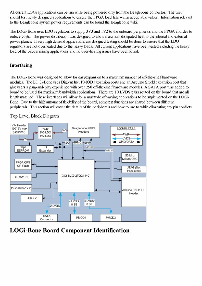
17. LED1 - general purpose LED
18. LED2 - general purpose LED
19. VDD Power LED
20. FPGA configuration done LED
21. Voltage input Header (5V Max)
22. Voltage output Header (3V3, 5V)
Figure LOGi-Bone Bottom component identification
1. Solder Jumper - Address Select for I2C IO Expander
2. LVDS pair silkscreen labels
3. Solder Jumper - Enable FPGA reset functionality on Push Button 1
4. Solder Jumper - FPGA configuration selection Mode Select Pins (Default = Slave configuration 11). Solder Jumper will pull
the pin low.
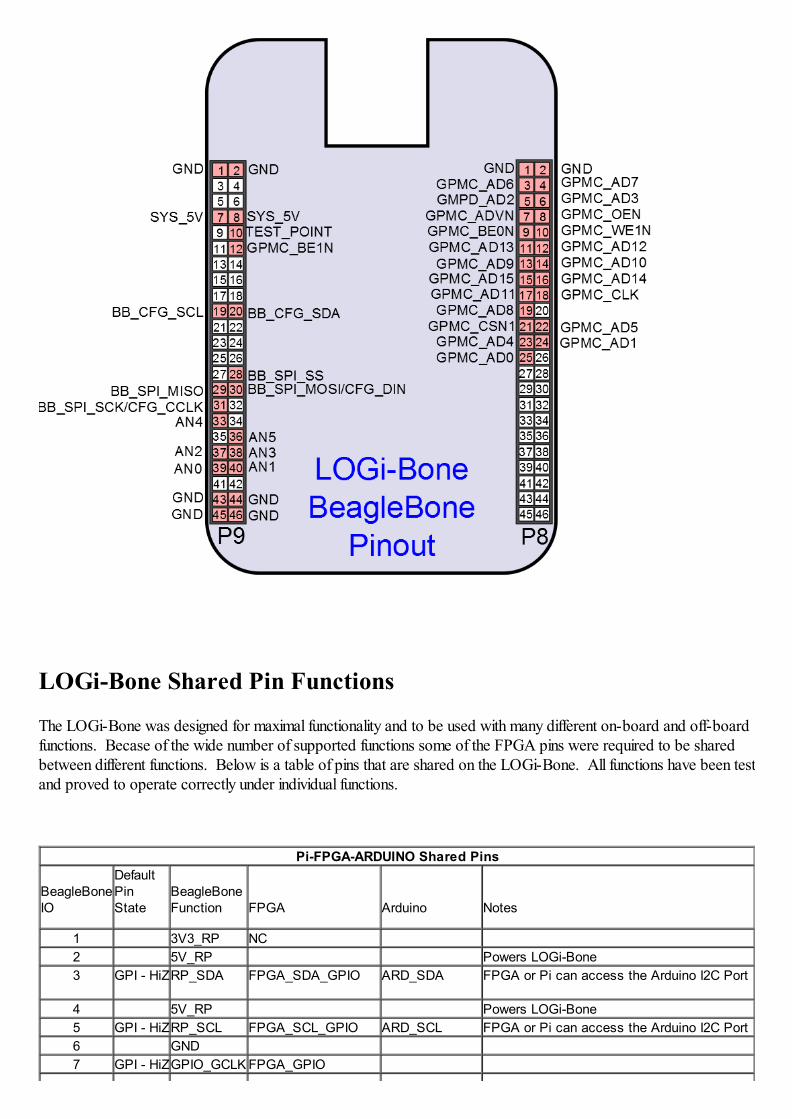
BeagleBone P8/P9 Connector Pin Usage
Below is an diagram that shows the pins that are used on P8/P9 of the beaglbone. The names of next to the pinscorrespond to the nets that are used in the schematics of the LOGi-Bone design and are indicative of the given pinsfunction.
For detailed pin connections you can download the latest schematics from the LOGi Github respository.
LOGi-Bone Shared Pin Functions
The LOGi-Bone was designed for maximal functionality and to be used with many different on-board and off-boardfunctions. Becase of the wide number of supported functions some of the FPGA pins were required to be sharedbetween different functions. Below is a table of pins that are shared on the LOGi-Bone. All functions have been testand proved to operate correctly under individual functions.
Pi-FPGA-ARDUINO Shared Pins
BeagleBoneIO
DefaultPinState
BeagleBoneFunction FPGA Arduino Notes
1 3V3_RP NC
2 5V_RP Powers LOGi-Bone
3 GPI - HiZRP_SDA FPGA_SDA_GPIO ARD_SDA FPGA or Pi can access the Arduino I2C Port
4 5V_RP Powers LOGi-Bone
5 GPI - HiZRP_SCL FPGA_SCL_GPIO ARD_SCL FPGA or Pi can access the Arduino I2C Port
6 GND
7 GPI - HiZGPIO_GCLK FPGA_GPIO

8 GPI - HiZRP_TX FPGA_GPIO_RX ARD_Master_RXFPGA or Pi can access the Arduino Uart Port
9 GND
10 GPI - HiZRP_RX FPGA_GPIO_TX ARD_Master_TX FPGA or Pi can access the Arduino Uart Port
11 GPI - HiZGPIO_GEN0FPGA_MODE0_GPIO
12 GPI - HiZGPIO_GEN1FPGA_MODE1_GPIO
13 GPI - HiZGPIO_GEN2FPGA_GPIO
14 GND
15 GPI - HiZGPIO_GEN3FPGA_GPIO
16 GPI - HiZGPIO_GEN4FPGA_INITB_GPIO
17 3V3_RP
18 GPI - HiZGPIO_GEN5FPGA_PROGB FPGA pin cannot be used as GPIO (Reset)
19 GPI - HiZSPI_MOSI FPGA_MOSI_GPIO
20 GND
21 GPI - HiZSPI_MISO FPGA_MISO_GPIO
22 GPI - HiZGPIO_GEN6FPGA_DONE FPGA pin cannot be used as GPIO
23 GPI - HiZGPIO_SCLK FPGA_SCK_GPIO
24 GPI - HiZSPI_CE0N FPGA
25 GND
26 GPI - HiZSPI_CE1N FPGA_GPIO
BeagleBone EMMC - GPMC - HDMI Functionality
The LOGi-Bone was initially designed for functionality with the BeagleBone White. The BeagleBone Black wasdesigned soon after with EMMC and HDMI functionality. We made adaptions the the LOGi-Bone design forfunctionality with the Black and the White and some design considerations were requiremed that focuses on GPMCand HDMI functionality.
The BeagleBone Black design shares pin functionality and allows for multiplexing of specific functions on each pin.The BeagleBone Black SRM section "7.1 Expansion Connectors" lists the pin sharing functionality.
BBB Peripheral Priorities in the LOGi-Bone Design
Priority of peripherals was designed for 1) GPMC high bandwidth interface 2) HDMI using the LCD pins.
The GPMC bus allow for a high bandwidth interface between the FPGA and the ARM processor. The currentLOGi GPMC driver support a bandwidth of up to 70 MB/s. The GPMC bus allows for many high performanceapplications utilizing this high speed link and was designed as high priority in the LOGi-Bone design.
The HDMI output on the BeagleBone black allows for a standalone computer experience for users. The LOGi-Team has plan to fully utilize the desktop feature that the HDMI video output enables. The LOGi-Team hasdesigned Virutal Components that give the LOGi-bone users a graphical interface to and from the FPGA using theHDMI output of the BeagleBone Black.
EMMC with the LOGi-Bone / BBB
Unfortunately, the EMMC port is shared with the GPMC bus and cannot be used simultaneously with GPMCfunctionality. It is possible for the user to implment the EMMC functionality, but requires that the SPI port be usedas the communication interface between the FPGA and the BBB. The SPI interface is much lower bandwidth thanthe GPMC, but will allow for EMMC, HDMI and LOGI-Bone FPGA functionality to occurr simultaneously.
PMOD Expansion Port

There are 2 x Digilent Inc. PMOD ports populated on the LOGi-Bone. The PMOD ports allow for a wide array ofCOTS modules to easily be interfaced with the LOGi-Bone. A listing of all currently available Digilent Inc. PMODmodules can be found on their site. More 3rd party PMOD modules can be found by searching on google.
The LOGi-Bone has only 2 PMODs and the LOGi-Pi has 4 PMODs. The LOGi-Bone design differs from theLOGi-Pi in that there were extra pins needs to implement the GPMC parallel bus between the FPGA and theBeaglebone.
Arduino Expansion Port
An Arduino header is used to expand the on-board capability of the LOGi-Bone with more than 200 COTS arduinoshields currently on the market. The LOGi-Bone arduino header supports UNO, DUEM and DUE Arduinoheaders. Note that only 3V3 Arduino Shields are supported as there is no logic level translation on the LOGi-Bone board. The latest Arduino shield specification states that arduino shields should be designed using the IOREFpin that swithches the logic level of the Arduino shield to support the UNO (5V) or the DUE (3V3). It is the usersresponsibility to ensure that shields that are to be used with the LOGi-Bone are 3V3 logic.
For details of the IOREF shield Pin functionality the arduino UNO board specifications page or the Arduino DUEspecifications page. Excerpts from the given pages are as follows:
"Shields will be compatible with both the board that uses the AVR, which operates with 5V and with theArduino Due that operates with 3.3V.""IOREF. This pin on the Arduino board provides the voltage reference with which the microcontrolleroperates. A properly configured shield can read the IOREF pin voltage and select the appropriate powersource or enable voltage translators on the outputs for working with the 5V or 3.3V."
The Arduino header can optionally be accessed directly by the Beaglebone either by direct shared connections orindirectly through the FPGA. This allows for direct use of the Beaglebone's SPI, I2C, UART hardware to directlytalk to the Arduino shields. Alternatively the shields can be accessed directly by the FPGA which can then beaccessed by the Beaglebone.
See ADC Functionality and Wiring for details on the Arduino ADC pins.
ADC Functionality and Wiring
LOGi-Bone RA3 and later revisions only
The LOGi-Bone impements 6 ADC input pins that interface directly to the BBB ADC pins. A voltage divider isused on these pins to drop the voltage of the Analog voltage to within the limites of the BBB ADC voltagespecification of 1.8V.
Additionally the user may jumper the Arduino AN0-AN6 pins to a PMOD ADC so that the FPGA can directlyaccess the ADC values. P6 is an unpoplulated header on the LOGi-Bone that the user can wire directly to aPMOD port of FPGA ADC access. Digilent Inc. Carries a variety of ADC PMOD devices.

SATA Expansion Port
The SATA connectors on the LOGi-Boards were not implemented to communicate with SATA devices, but toprovide an easy to use, low cost LVDS expansion port. SATA interfaces are very widely used which make thecables and connectors very low cost and easily accessible.
A high bandwidth interface was designed onto the LOGi-Bone using a SATA connector. SATA connectors arevery low cost and SATA cables are readily available and cheap. The SATA connector allows for a low costimpedance controlled connection to externally designed modules that are designed using a SATA connector. TheLOGi Team anticipates designing high bandwidth modules such as LVDS camera, LVDS ADC, etc.
Two differential pairs are routed to the SATA connector. The differential pairs are routed as 100 ohm differentialand 50 ohm single ended pairs. The differential pairs are matched in length to within .015" length from each other.
LVDS signal usage
Additional LVDS differential pairs were routed on the board to allow for experimentation and work with furthermulti-channel LVDS applications that require more than is available with the SATA connector. Eight additionaldifferential pairs were routed to PMOD3 and PMOD4 connectors on the board. The differential pairs are routed as100 ohm differential and 50 ohm single ended pairs. The differential pairs are matched in length to within .015"length from each other. These additional differential pairs were also routed to match the length of the SATAdifferential pairs so that they could be used in the same applications as needed.
The PMOD connectors are not optimized for use in LVDS application based on the differential signal length the iscreated by the connectors being 90 degree angles. The upper and lower rows on the PMOD connector do NOTmatch in length and if the PMOD connector is to be used this differential length in path should be taken into account.

The PMOD connectors are not optimal for differential signals as they are not capable of maintaining the differentialimpedance based on the large separation of the signal throughout the length of the connector. It is possible tominimize this mismatch by replacing the PMOD connectors with low profile .100" vertical headers that will shortenthe path of separation therefore minimizing the impedance mismatch and allow for higher bandwidth interfaces. Foroptimal performance using the LVDS signals on PMOD3 and PMOD4 it is recommended that LVDS signals bedirectly soldered to the header pads to eliminate the impedance mismatch that occurs throughout the connector.
Push Button Usage
Two push button switches are provided on the LOGi-Bone. The pushbuttons are configured active high and andiscrete 10k ohm pull-up resistor is populated on-board to eliminate the need for configuring and used the on-chippull-up resistors. Additionally a DNP capacitor footprint is provided to allow users to install a capacitor for analogdebounce functionality. It is recommended the soft debounce logic be used in HDL, if the debounce functionality isnot enable by use of an installed capacitor,
DIP Switch Usage
A two position DIP switch is used on the LOGi-Bone. It is anticipated that the DIP switch be used for modecontrol and other general purpose usage.
LED Usage
Two general purpose LED's are used on the LOGi-Bone. Due to the limited pin availability on the FPGA TQFPpackage the LED pins are also shared with two rarely used PWM inputs on the Arduino Shield (RA2.1 only).
JTAG Interface
A unpopulated JTAG header is available on the LOGi-Bone. The JTAG header is contains the Digilent Inc. 6 pinfunction pinout and is a .100" 6 pin header. The Digilent Inc JTAG adapters or xinlinx flying lead adapters can beused to interface with the FPGA through the JTAG connection. The JTAG connection allows for directprogramming FPGA or onboard Flash memory, additionally chipscope can be used for deep debug and analysis.
Device Tree requirements
The Device tree is the beaglebone blacks method of properly configuring and muxing the onboard hardwareperipherals that will be used for a given configuration. In order for the LOGi drivers to properly function the BBBmust be configured with an appropriate device tree overlay to configure the GPMC, GPIO, SPI, etc. For specificinformation about the device tree, how it works and how to create your own device tree overlays, see adafruit'sexisting guide.
The Logi pre-configured image contains a device tree overlay that will properly configure the device tree. The last R1 version ofthe pre-configured Logi-Image is setup to automatically setup the device-tree each time it boots.
Kickstarter Early Bird Boards auto device-tree setup
The kickstarter boards will require that the user run a script that sets up the onboard eeprom the to setup the autodevice-tree setup.

Example Device-Tree overlays and scripts
The LOGi device tree overlay files and setup script can be found in the logi-Kernel github repository.
LOGi-bone template driver
The Logi-kernel repository hosts the source for a template driver for the LOGI-bone. This driver exposes twointerfaces in the /dev folder.
1. logibone : the /dev/logibone interface is the programming interface for the LOGI-bone. By doing direct
access to this character device you can program the FPGA (sudo dd if=<bitfile>.bit of=/dev/logibonebs=4M).
2. logibone-mem : The /dev/logibone-mem interfaces gives acces to the full address space of the FPGA whenusing a wishbone based architecture. This interface can be used for communication with the logic withbandwidth between 4MB/s and 70MB/s depending on the amount of data transferred. This interface will suit
the need of most users to get a basic but fast communication running with the FPGA.
The template driver is modular enough so that you can use its source code to start writing your own driver for aspecific application.
Compiling the template driver
To compile the template driver you first need to install the kernel source of your distribution one your linux machine.The following instruction will work for a Ubuntu machine (tested on 12.04 LTS) compiling for a Ubuntun distributionrunning on the beaglebone.
Installing a the toolchain
The default toolchain to cross-compile the linux kernel for the beaglebone is Linaro. You can install linaro on aUbuntu machine by running the following command.
sudo apt-get install gcc-arm-linux-gnueabihf
Installing the kernel source
The kernel source can be installed from git. The following command will run to install kernel 3.8.13. You may adaptthe command for a new kernel/older kernel.
git clone -b am33x-v3.8 https://github.com/RobertCNelson/linux-dev.git #cloning am33x-v3.8 branch
cd linux-dev
1. edit version.sh with kernel version and build
./build_kernel.sh
1. this may take a while
2. at some point you'll get a menuconfig prompt (blue screen), just hit exit if you don't need to add additionaldrivers

If everything goes well you should en-up with a KERNEL directory containing the kernel source and producedbinaries.
Installing and compiling logibone template driver
The source of the kernel driver can be clone from the logi-kernel repository.
git clone https://github.com/fpga-logi/Logi-kernel.git
cd Logi-kernel/beaglebone-black
Now you have to edit the build_module.sh with the path of your toolchain (arm-linux-gnueabihf if you are using theUbuntu kernel and Linaro toolchain) and the path of your kernel (should be the KERNEL folder of the repositoryinstalled in the "Installing the kernel source" step).
Once the build_module.sh file is edited you just have to do a
./build_module.sh
and you should end up with the *.ko file of the kernel module in the logibone_ra2 folder. This will produce tomodules suffixed _dma and _dm. The _dm can expose more bandwidth but requires more processor involvement,the _dma module uses the EDMA which performs transfer in parallel with computation. The _dma exposes lessbandwidth for small transfer but free the CPU while transferring, for large transfer the EDMA method will workbetter.
Creating your own template driver
Let say you want to use the FPGA as a framebuffer for a connected camera, you can design your own driver basedon the template driver and implement a framebuffer driver. Designing your own driver will help you get the bestperformance for a specific application but the template driver exposes enough functionality so you can startprototyping without messing with kernel module programming.
Programming the FPGA from the Beaglebone
The template driver from the github exposes a programming interface in directory "/dev" called logibone(/dev/logibone). This character device writes incoming bytes to the FPGA through its serial programming interface.Loading a bitsream to the FPGA can be performed in the following ways:
1. use the dd command : sudo dd if=<bitfile-path> of=/dev/logibone bs=4M (ex : sudo dd if=logi_camera.bit
of=/dev/logibone bs=4M). The bs=4M argument is mandatory as it will force the interface to load all the
configuration file in one access to the programming interface.2. use the logi_loader script : sudo logi_loader <bitfile-path> (ex : sudo logi_loader logi_camera.bit). Tihs script
just calls the dd command with the aforementionned arguments.
The pre-configured LOGi linux images come with the driver installed and the logi_loader script installed by default. The device tree configuration adn driver loading must be performed prior to running the FPGA configuration.
Manually installing the LOGi-Loader

The logi_loader script is available from the Logi_loader/beaglebone repository. Just copy the beaglebone directoryto the beaglebone filesystem and run the install script. The logi_loader will be installed into /usr/bin and can then beaccessed globally to load bitstream files from any location by runing the command from the command line.
Process for running the LOGi-Loader:
1) After booting linux image run the device tree setup script: $ sudo ./setup_device_tree.sh
2) Run the LOGi-Loader to load your FPGA bitstream file: $ sudo logi_loader "name.bit"
BeagleBone to FPGA Interfaces
BBB GPMC to FPGA Interface
The deafault interface for communication between the BBB and the FPGA is the GPMC bus. For details aboutoperation and implementation of the GPMC bus within the AM335x processor see section 7.1 GPMC of theAM335x reference manual.
Current GPMC performance with the LOGI Drivers
The current LOGI GPMC drivers have a theoretical bandwidth of 76MB/s and measured up to 69MB/s in user space for transfer of
128KB blocks. Our kernel driver gives access to the whole address space of the FPGA with EDMA but can be re-written to be
application specific and get better bandwidth. For now the overhead for switching from user-space to kernel space impacts a lot the
performance, thus writing an application specific kernel driver (ours uses EDMA and burst access) with interrupt for transfer
generated by the FPGA could get you close to theoretical bandwidth.
LOGI GPMC driver implementation details
Specific documentaiton and implmentation details will be hosted on this specific LOGI GPMC driver wiki page.
Useful Links
Logi - Repository - Projects, Libraries, Drivers
Logi - Repository
Logi-Bone Schematics
Logi-Bone Schematics
Logi-Bone User Guide -Logi-Bone documentation
Logi-Bone User Guide
Logi Projects wiki - LOGI and Users projects will be documentedhere

Logi Projects wiki
Retrieved from "http://valentfx.com/wiki/index.php?title=Logi-Bone_User_Guide&oldid=673"Category: Logi-Bone
This page was last modified on 1 May 2014, at 10:32.
This page has been accessed 6,577 times.