lmh6514 digital controlled variable gain - texas instruments
TRANSCRIPT
User's GuideSNOA524A–April 2008–Revised May 2013
AN-1828 LMH6514 Digital Controlled Variable GainAmplifier Evaluation Board
1 General Description
The LMH6514 evaluation board (part # LMH6514SQEVAL) is designed to aid in the characterization ofTexas Instruments high speed LMH6514 digital controlled variable gain amplifiers (DVGA).
Use the evaluation board as a guide for high frequency layout and as a tool to aid in device testing andcharacterization.
2 Basic Operation
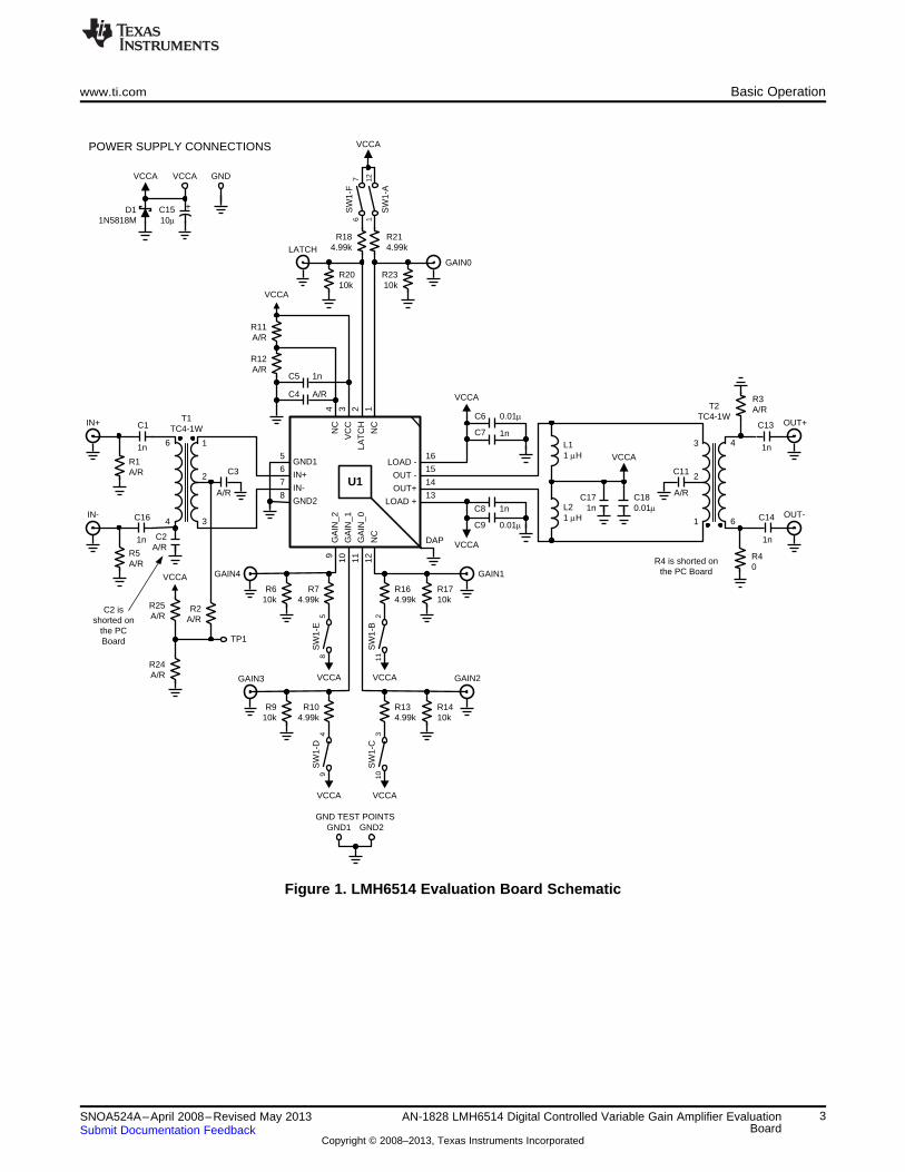
The LMH6514 DVGA has differential inputs and differential outputs. The LMH6514 will also support single-ended to differential conversion with no transformer required on the input. To aid evaluation with 50 Ωsingle-ended test equipment the LMH6514 evaluation board provides for input and output transformers.For driving the evaluation board from a differential source, symmetrical signal paths are provided. Bothinput and output paths support fully differential signal paths. For component locations refer to theschematic in Figure 1.
The evaluation board uses end mounted SMA connectors. On the IN+ input, resistor R1 provides inputtermination. The analog supply (VCCA) can be from 4 V to 5.25 V. The capacitor C5 is a supply bypasscapacitor and should be low ESR ceramic. Resistors R11 and R12 as well as capacitor C4 should be leftempty.
The LMH6514 evaluation board is designed for transformers wtih DC isloation between the primary andsecondary windings. If baluns (transmission line transformers with no DC blocking) are used make sure tohave DC isolation for all transformer pads.
Transformer T1 can provide both impedance matching as well as single ended to differential conversion.The 2:1 (4:1 impedance) transformer matches 50 Ω equipment with the 200 Ω input impedance of theLMH6514 DVGA and there is an optional capacitor at C3 if additional stability is required. Do not connectthe transformer secondary winding directly to ground. The LMH6514 has a self biased input commonmode voltage of approximately 1.3 V. The amplifier will bias up to the optimal input common mode point.The resistors R2, R24, and R25 are normally left empty. These resistors can be used to force theLMH6514 input common mode to a value different than it's self biased state. Most applications will notrequire this function.
If using a transmission line transformer for T1, capacitor C1 is necessary to preserve the proper inputcommon mode voltage. For single-ended inputs to the amplifier, see Figure 7 and Figure 8.
The LMH6514 evaluation board is shipped with a transformer to facilitate testing with single-endedequipment. To drive the LMH6514 evaluation board with a differential signal, transformer T1 must beremoved. Then, load capacitor C1 and C16 and cut the trace connecting the capacitor C2. R1 and R5should be loaded with appropriate valued resistors (normally 50 Ω). The C3 capacitor is not needed forthis case and the transformer pads should be shorted with a low inductance wire: pad 6 to pad 1 and pad4 to pad 3.
On the output side of the board is transformer T2. C11 isolates the output common mode voltage from theoutput transformer primary windings. The output coupling capacitors C13 and C14 are necessary forBalun transformers that provide no DC isolation between the primary and secondary windings, and arealso necessary when driving differential loads.
All trademarks are the property of their respective owners.
1SNOA524A–April 2008–Revised May 2013 AN-1828 LMH6514 Digital Controlled Variable Gain Amplifier EvaluationBoardSubmit Documentation Feedback
Copyright © 2008–2013, Texas Instruments Incorporated
Basic Operation www.ti.com
For differential output signals remove transformer T2. Capacitor C11 can be left empty. Do not installresistor R4. Using the transformer T2 pads, place coupling capacitors between pads 3 and 4 and betweenpads 1 and 6 where the transformer would have been. These should be low ESR ceramic capacitors witha value of 1 nF. These output coupling capacitors are necessary to isolate the output common modevoltage of the LMH6514 from the test equipment. The pads for capacitors C13 and C14 can be used asseries output matching resistors. There is no copper between transformer pad #6 and C14. A lowimpedance short will have to be added manually. Resistors R3 and R4 are normally left empty in thisconfiguration.
The evaluation board supports two gain options. As shipped, the evaluation board provides for a low gain,200 Ω output impedance configuration. In order to use the high gain 400 Ω configuration, the traces frompins 13 and 16 to VCCA can be cut. For a detail of the trace cuts required, see Figure 6.
SW1 is used to set the three gain control bits. When the Latch position of SW1 is in 0 or OFF position,changes in the Gain 2 to Gain 5 bits are processed by the LMH6514 (see the paragraph below). When thelatch switch is in 1 or ON position, the last loaded state is held and gain bit switch changes have no effect.Landings for SMA connectors are also provided for high speed triggering of the gain bits.
Since the same PC board is also used for the LMH6515 DVGA, the markings on SW1 are not the sameas the pin assignments for the LMH6514. On the SW1, Gain_4 on the board corresponds to Gain_2 onthe LMH6514, Gain_3 on the board corresponds to Gain _1 on the LMH6514 and Gain_2 corresponds toGain_0 on the LMH6514.
The LMH6514 evaluation board is a four layer board; all four layers are detailed in Figure 2 throughFigure 5.
2 AN-1828 LMH6514 Digital Controlled Variable Gain Amplifier Evaluation SNOA524A–April 2008–Revised May 2013Board Submit Documentation Feedback
Copyright © 2008–2013, Texas Instruments Incorporated
U16
5
7
8
15
16
14
13
VC
C
NC
LAT
CH
NC
34 2 1
OUT -
LOAD -
OUT+
LOAD +
IN+
GND1
IN-
GND2
GA
IN_1
GA
IN_2
GA
IN_0
NC
DAP
C4 A/R
C5 1n
R12A/R
R11A/R
VCCA
109 11 12
R74.99k
R610k
211
SW
1-B
VCCA
R164.99k
R1710k
R104.99k
R910k
49
SW
1-D
VCCA
310
SW
1-C
VCCA
R134.99k
R1410k
GND2GND1GND TEST POINTS
R2310k
R2010k
GAIN1GAIN4
GAIN2GAIN3
GAIN0
LATCHR18
4.99kR214.99k
58
SW
1-E
VCCA
VCCA
76
SW
1-F
121
SW
1-A
+C1510P
VCCA
POWER SUPPLY CONNECTIONS
D11N5818M
VCCA GND
R2A/R
R25A/R
R24A/R
VCCA
TP1
3
2
1
C3
A/R
4
6
T1TC4-1W
C2A/R
C16
1n
C1
1n
R5A/R
R1A/R
IN-
IN+
1
2
3
C11
A/R
6
4
T2TC4-1W
C14
1n
C13
1n
R40
R3A/R
OUT-
OUT+
1nC8
0.01PC9
1n
C6 0.01P
C7
VCCA
VCCA
L21 PH
L11 PH
C171n
C180.01P
VCCA
C2 is shorted on
the PCBoard
R4 is shorted onthe PC Board
www.ti.com Basic Operation
Figure 1. LMH6514 Evaluation Board Schematic
3SNOA524A–April 2008–Revised May 2013 AN-1828 LMH6514 Digital Controlled Variable Gain Amplifier EvaluationBoardSubmit Documentation Feedback
Copyright © 2008–2013, Texas Instruments Incorporated

Basic Operation www.ti.com
Figure 2. Evaluation Board Top Layer
Figure 3. Evaluation Board Bottom Layer
4 AN-1828 LMH6514 Digital Controlled Variable Gain Amplifier Evaluation SNOA524A–April 2008–Revised May 2013Board Submit Documentation Feedback
Copyright © 2008–2013, Texas Instruments Incorporated

www.ti.com Basic Operation
Figure 4. Evaluation Board Layer 2
Figure 5. Evaluation Board Layer 3
5SNOA524A–April 2008–Revised May 2013 AN-1828 LMH6514 Digital Controlled Variable Gain Amplifier EvaluationBoardSubmit Documentation Feedback
Copyright © 2008–2013, Texas Instruments Incorporated

Basic Operation www.ti.com
Figure 6. Trace Cuts for High Gain (400 Ω Load) Operation
Figure 7. Single-Ended Input – No Transformer
6 AN-1828 LMH6514 Digital Controlled Variable Gain Amplifier Evaluation SNOA524A–April 2008–Revised May 2013Board Submit Documentation Feedback
Copyright © 2008–2013, Texas Instruments Incorporated

GAIN 1-5
200
5
LATCH
LMH6514VIN
R1RIN = R1 || 200
VCM = 1.4V
C1
WITHOUT THIS CAPACITOR THE INPUT WILL NOT
FUNCTION
VCC
www.ti.com Basic Operation
Figure 8. Schematic for Single-Ended Input
7SNOA524A–April 2008–Revised May 2013 AN-1828 LMH6514 Digital Controlled Variable Gain Amplifier EvaluationBoardSubmit Documentation Feedback
Copyright © 2008–2013, Texas Instruments Incorporated

IMPORTANT NOTICE
Texas Instruments Incorporated and its subsidiaries (TI) reserve the right to make corrections, enhancements, improvements and otherchanges to its semiconductor products and services per JESD46, latest issue, and to discontinue any product or service per JESD48, latestissue. Buyers should obtain the latest relevant information before placing orders and should verify that such information is current andcomplete. All semiconductor products (also referred to herein as “components”) are sold subject to TI’s terms and conditions of salesupplied at the time of order acknowledgment.
TI warrants performance of its components to the specifications applicable at the time of sale, in accordance with the warranty in TI’s termsand conditions of sale of semiconductor products. Testing and other quality control techniques are used to the extent TI deems necessaryto support this warranty. Except where mandated by applicable law, testing of all parameters of each component is not necessarilyperformed.
TI assumes no liability for applications assistance or the design of Buyers’ products. Buyers are responsible for their products andapplications using TI components. To minimize the risks associated with Buyers’ products and applications, Buyers should provideadequate design and operating safeguards.
TI does not warrant or represent that any license, either express or implied, is granted under any patent right, copyright, mask work right, orother intellectual property right relating to any combination, machine, or process in which TI components or services are used. Informationpublished by TI regarding third-party products or services does not constitute a license to use such products or services or a warranty orendorsement thereof. Use of such information may require a license from a third party under the patents or other intellectual property of thethird party, or a license from TI under the patents or other intellectual property of TI.
Reproduction of significant portions of TI information in TI data books or data sheets is permissible only if reproduction is without alterationand is accompanied by all associated warranties, conditions, limitations, and notices. TI is not responsible or liable for such altereddocumentation. Information of third parties may be subject to additional restrictions.
Resale of TI components or services with statements different from or beyond the parameters stated by TI for that component or servicevoids all express and any implied warranties for the associated TI component or service and is an unfair and deceptive business practice.TI is not responsible or liable for any such statements.
Buyer acknowledges and agrees that it is solely responsible for compliance with all legal, regulatory and safety-related requirementsconcerning its products, and any use of TI components in its applications, notwithstanding any applications-related information or supportthat may be provided by TI. Buyer represents and agrees that it has all the necessary expertise to create and implement safeguards whichanticipate dangerous consequences of failures, monitor failures and their consequences, lessen the likelihood of failures that might causeharm and take appropriate remedial actions. Buyer will fully indemnify TI and its representatives against any damages arising out of the useof any TI components in safety-critical applications.
In some cases, TI components may be promoted specifically to facilitate safety-related applications. With such components, TI’s goal is tohelp enable customers to design and create their own end-product solutions that meet applicable functional safety standards andrequirements. Nonetheless, such components are subject to these terms.
No TI components are authorized for use in FDA Class III (or similar life-critical medical equipment) unless authorized officers of the partieshave executed a special agreement specifically governing such use.
Only those TI components which TI has specifically designated as military grade or “enhanced plastic” are designed and intended for use inmilitary/aerospace applications or environments. Buyer acknowledges and agrees that any military or aerospace use of TI componentswhich have not been so designated is solely at the Buyer's risk, and that Buyer is solely responsible for compliance with all legal andregulatory requirements in connection with such use.
TI has specifically designated certain components as meeting ISO/TS16949 requirements, mainly for automotive use. In any case of use ofnon-designated products, TI will not be responsible for any failure to meet ISO/TS16949.
Products Applications
Audio www.ti.com/audio Automotive and Transportation www.ti.com/automotive
Amplifiers amplifier.ti.com Communications and Telecom www.ti.com/communications
Data Converters dataconverter.ti.com Computers and Peripherals www.ti.com/computers
DLP® Products www.dlp.com Consumer Electronics www.ti.com/consumer-apps
DSP dsp.ti.com Energy and Lighting www.ti.com/energy
Clocks and Timers www.ti.com/clocks Industrial www.ti.com/industrial
Interface interface.ti.com Medical www.ti.com/medical
Logic logic.ti.com Security www.ti.com/security
Power Mgmt power.ti.com Space, Avionics and Defense www.ti.com/space-avionics-defense
Microcontrollers microcontroller.ti.com Video and Imaging www.ti.com/video
RFID www.ti-rfid.com
OMAP Applications Processors www.ti.com/omap TI E2E Community e2e.ti.com
Wireless Connectivity www.ti.com/wirelessconnectivity
Mailing Address: Texas Instruments, Post Office Box 655303, Dallas, Texas 75265Copyright © 2013, Texas Instruments Incorporated