lm3480 100-ma, sot-23, quasi low-dropout linear voltage
TRANSCRIPT

COUT
0.1 µF
LM3480IM3-5.0
3
2 15 V, 100 mA OUT6.5 V IN
CIN
0.1 µF
Product
Folder
Sample &Buy
Technical
Documents
Tools &
Software
Support &Community
LM3480SNVS011H –JUNE 1999–REVISED SEPTEMBER 2015
LM3480 100-mA, SOT-23, Quasi Low-Dropout Linear Voltage Regulator1 Features 3 Description
The LM3480 is an integrated linear voltage regulator.1• Input Voltage Range: up to 30 V
It features operation from an input as high as 30 V• 3.3-V, 5-V, 12-V, and 15-V Versions Available and an ensured maximum dropout of 1.2 V at the full• Packaged in the Tiny 3-Lead SOT-23 Package 100-mA load. Standard packaging for the LM3480 is
the 3-lead SOT-23 package.• 30-V Maximum Input for Operation• 1.2-V Ensured Maximum Dropout Over Full Load The 5-V, 12-V, and 15-V members of the LM3480
and Temperature Ranges series are intended as tiny alternatives to industrystandard LM78Lxx series and similar devices. The• 100-mA Ensured Minimum Load Current1.2-V quasi-low dropout of LM3480 series devices• ±5% Ensured Output Voltage Tolerance Over Full makes them a nice fit in many applications where the
Load and Temperature Ranges 2-V to 2.5-V dropout of LM78Lxx series devices• −40 to +125°C Junction Temperature Range for precludes their (LM78Lxx series devices) use.
Operation The LM3480 series also features a 3.3-V member.The SOT-23 packaging and quasi-low dropout2 Applications features of the LM3480 series converge in this deviceto provide a very nice, very tiny, 3.3-V, 100-mA bias• Tiny Alternative to LM78Lxx Series and Similarsupply that regulates directly off the system 5-V ±5%Devicespower supply.• Tiny 5-V ±5% to 3.3-V, 100-mA Converter
• Post Regulator for Switching DC/DC Converter Device Information(1)
• Bias Supply for Analog Circuits PART NUMBER PACKAGE BODY SIZE (NOM)LM3480 SOT-23 (3) 2.92 mm × 1.30 mm
(1) For all available packages, see the orderable addendum atthe end of the data sheet.
space
space
space
Typical Application Circuit
1
An IMPORTANT NOTICE at the end of this data sheet addresses availability, warranty, changes, use in safety-critical applications,intellectual property matters and other important disclaimers. PRODUCTION DATA.

LM3480SNVS011H –JUNE 1999–REVISED SEPTEMBER 2015 www.ti.com
Table of Contents7.3 Feature Description................................................. 101 Features .................................................................. 17.4 Device Functional Modes........................................ 102 Applications ........................................................... 1
8 Application and Implementation ........................ 113 Description ............................................................. 18.1 Application Information............................................ 114 Revision History..................................................... 28.2 Typical Application ................................................. 115 Pin Configuration and Functions ......................... 3
9 Power Supply Recommendations ...................... 136 Specifications......................................................... 410 Layout................................................................... 136.1 Absolute Maximum Ratings ...................................... 4
10.1 Layout Guidelines ................................................. 136.2 ESD Ratings.............................................................. 410.2 Layout Example .................................................... 136.3 Recommended Operating Conditions....................... 4
11 Device and Documentation Support ................. 146.4 Thermal Information .................................................. 411.1 Community Resources.......................................... 146.5 Electrical Characteristics: LM3480-3.3, LM3480-5 ... 511.2 Trademarks ........................................................... 146.6 Electrical Characteristics: LM3480-12, LM3480-15 .. 611.3 Electrostatic Discharge Caution............................ 146.7 Typical Characteristics .............................................. 711.4 Glossary ................................................................ 147 Detailed Description ............................................ 10
12 Mechanical, Packaging, and Orderable7.1 Overview ................................................................. 10Information ........................................................... 147.2 Functional Block Diagram ....................................... 10
4 Revision HistoryNOTE: Page numbers for previous revisions may differ from page numbers in the current version.
Changes from Revision G (February 2015) to Revision H Page
• Replaced Functional Block Diagram .................................................................................................................................... 10• Changed text of External Capacitors subsection ................................................................................................................ 11• Changed text of Output Capacitor subsection ..................................................................................................................... 11
Changes from Revision F (December 2014) to Revision G Page
• Changed pin numbers indicated in Typical Application drawing; fix typos............................................................................. 1• Deleted soldering specs - found in POA ................................................................................................................................ 4• Changed Handling Ratings to ESD Ratings format ............................................................................................................... 4
Changes from Revision E (March 2013) to Revision F Page
• Added Pin Configuration and Functions section, Handling Rating table, Feature Description section, DeviceFunctional Modes, Application and Implementation section, Power Supply Recommendations section, Layoutsection, Device and Documentation Support section, and Mechanical, Packaging, and Orderable Informationsection; add updated Thermal Information ............................................................................................................................. 1
Changes from Revision D (March 2013) to Revision E Page
• Changed layout of National Data Sheet to TI format ............................................................................................................. 9
2 Submit Documentation Feedback Copyright © 1999–2015, Texas Instruments Incorporated
Product Folder Links: LM3480

LM3480www.ti.com SNVS011H –JUNE 1999–REVISED SEPTEMBER 2015
5 Pin Configuration and Functions
DBZ Package3-Pin SOT-23
Top View
Pin FunctionsPIN
I/O DESCRIPTIONNAME NO.
OUT 1 O Output voltageIN 2 I Input voltage supplyGND 3 — Common ground
Copyright © 1999–2015, Texas Instruments Incorporated Submit Documentation Feedback 3
Product Folder Links: LM3480
LM3480SNVS011H –JUNE 1999–REVISED SEPTEMBER 2015 www.ti.com
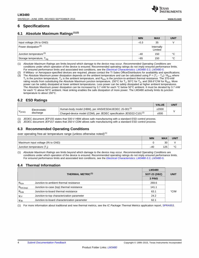
6 Specifications
6.1 Absolute Maximum Ratings (1) (2)
MIN MAX UNITInput voltage (IN to GND) –0.3 35 VPower dissipation (3) Internally
LimitedJunction temperature (3) –40 150 °CStorage temperature, Tstg −65 150 °C
(1) Absolute Maximum Ratings are limits beyond which damage to the device may occur. Recommended Operating Conditions areconditions under which operation of the device is ensured. Recommended operating ratings do not imply ensured performance limits.For ensured performance limits and associated test conditions, see the Electrical Characteristics: LM3480-3.3, LM3480-5.
(2) If Military- or Aerospace-specified devices are required, please contact the TI Sales Office/Distributors for availability and specifications.(3) The Absolute Maximum power dissipation depends on the ambient temperature and can be calculated using P = (TJ – TA) / RθJA where
TJ is the junction temperature, TA is the ambient temperature, and RθJA is the junction-to-ambient thermal resistance. The 370-mWrating results from substituting the Absolute Maximum junction temperature, 150°C for TJ, 50°C for TA, and 269.6°C/W for RθJA. Morepower can be safely dissipated at lower ambient temperatures. Less power can be safely dissipated at higher ambient temperatures.The Absolute Maximum power dissipation can be increased by 3.7 mW for each °C below 50°C ambient. It must be derated by 3.7 mWfor each °C above 50°C ambient. Heat sinking enables the safe dissipation of more power. The LM3480 actively limits its junctiontemperature to about 150°C.
6.2 ESD RatingsVALUE UNIT
Human-body model (HBM), per ANSI/ESDA/JEDEC JS-001 (1) ±2000ElectrostaticV(ESD) Vdischarge Charged-device model (CDM), per JEDEC specification JESD22-C101 (2) ±500
(1) JEDEC document JEP155 states that 500-V HBM allows safe manufacturing with a standard ESD control process.(2) JEDEC document JEP157 states that 250-V CDM allows safe manufacturing with a standard ESD control process.
6.3 Recommended Operating Conditionsover operating free-air temperature range (unless otherwise noted) (1)
MIN MAX UNITMaximum input voltage (IN to GND) 0 30 VJunction temperature (TJ) –40 125 °C
(1) Absolute Maximum Ratings are limits beyond which damage to the device may occur. Recommended Operating Conditions areconditions under which operation of the device is ensured. Recommended operating ratings do not imply ensured performance limits.For ensured performance limits and associated test conditions, see the Electrical Characteristics: LM3480-3.3, LM3480-5.
6.4 Thermal InformationLM3480
THERMAL METRIC (1) SOT-23 (DBZ) UNIT3 PINS
RθJA Junction-to-ambient thermal resistance 269.6RθJC(top) Junction-to-case (top) thermal resistance 141.1RθJB Junction-to-board thermal resistance 63.1 °C/WψJT Junction-to-top characterization parameter 24.2ψJB Junction-to-board characterization parameter 62.1
(1) For more information about traditional and new thermal metrics, see the IC Package Thermal Metrics application report, SPRA953.
4 Submit Documentation Feedback Copyright © 1999–2015, Texas Instruments Incorporated
Product Folder Links: LM3480

LM3480www.ti.com SNVS011H –JUNE 1999–REVISED SEPTEMBER 2015
6.5 Electrical Characteristics: LM3480-3.3, LM3480-5Typical and other limits apply for TA = TJ = 25°C, unless otherwise specified. Nominal output voltage (VNOM) = 3.3 V or 5V. (1) (2) (3)
VNOM = 3.3 V VNOM = 5 VPARAMETER TEST CONDITIONS UNIT
MIN TYP MAX MIN TYP MAXVIN = VNOM + 1.5 V 3.17 3.3 3.43 4.8 5 5.21 mA ≤ IOUT ≤ 100 mA
VOUT Output voltage VVIN = VNOM + 1.5 V1 mA ≤ IOUT ≤ 100 mA 3.14 3.46 4.75 5.25−40°C ≤ TJ ≤ 125°CVNOM + 1.5 V ≤ VIN ≤ 30 V 10 12IOUT = 1 mA
ΔVOUT Line regulation mVVNOM + 1.5 V ≤ VIN ≤ 30 VIOUT = 1 mA 25 25−40°C ≤ TJ ≤ 125°CVIN = VNOM + 1.5 V 20 2010 mA ≤ IOUT ≤ 100 mA
ΔVOUT Load regulation mVVIN = VNOM + 1.5 V10 mA ≤ IOUT ≤ 100 m 40 40−40°C ≤ TJ ≤ 125°CVNOM + 1.5 V ≤ VIN ≤ 30 V 2 2No Load
IGND Ground pin current mAVNOM + 1.5 V ≤ VIN ≤ 30 VNo Load, 4 4−40°C ≤ TJ ≤ 125°CIOUT = 10 mA 0.7 0.9 0.7 0.9
VIOUT = 10 mA 1 1−40°C ≤ TJ ≤ 125°CVIN - DropoutvoltageVOUT IOUT = 100 mA 0.9 1.1 0.9 1.1VIOUT = 100 mA 1.2 1.2−40°C ≤ TJ ≤ 125°C
VIN = 10 Ven Output noise voltage 100 150 µVrmsBandwidth: 10 Hz to 100 kHz
(1) A typical is the center of characterization data taken with TA = TJ = 25°C. Typicals are not ensured.(2) All limits are ensured. All electrical characteristics having room-temperature limits are tested during production with TA = TJ = 25°C. All
hot and cold limits are ensured by correlating the electrical characteristics to process and temperature variations and applying statisticalprocess control.
(3) All voltages except dropout are with respect to the voltage at the GND pin.
Copyright © 1999–2015, Texas Instruments Incorporated Submit Documentation Feedback 5
Product Folder Links: LM3480
LM3480SNVS011H –JUNE 1999–REVISED SEPTEMBER 2015 www.ti.com
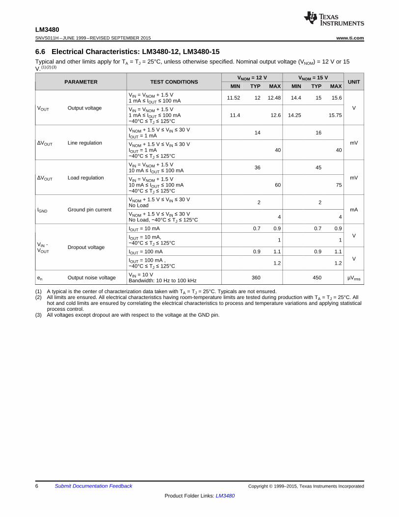
6.6 Electrical Characteristics: LM3480-12, LM3480-15Typical and other limits apply for TA = TJ = 25°C, unless otherwise specified. Nominal output voltage (VNOM) = 12 V or 15V. (1) (2) (3)
VNOM = 12 V VNOM = 15 VPARAMETER TEST CONDITIONS UNIT
MIN TYP MAX MIN TYP MAXVIN = VNOM + 1.5 V 11.52 12 12.48 14.4 15 15.61 mA ≤ IOUT ≤ 100 mA
VOUT Output voltage VVIN = VNOM + 1.5 V1 mA ≤ IOUT ≤ 100 mA 11.4 12.6 14.25 15.75−40°C ≤ TJ ≤ 125°CVNOM + 1.5 V ≤ VIN ≤ 30 V 14 16IOUT = 1 mA
ΔVOUT Line regulation mVVNOM + 1.5 V ≤ VIN ≤ 30 VIOUT = 1 mA 40 40−40°C ≤ TJ ≤ 125°CVIN = VNOM + 1.5 V 36 4510 mA ≤ IOUT ≤ 100 mA
ΔVOUT Load regulation mVVIN = VNOM + 1.5 V10 mA ≤ IOUT ≤ 100 mA 60 75−40°C ≤ TJ ≤ 125°CVNOM + 1.5 V ≤ VIN ≤ 30 V 2 2No Load
IGND Ground pin current mAVNOM + 1.5 V ≤ VIN ≤ 30 V 4 4No Load, −40°C ≤ TJ ≤ 125°CIOUT = 10 mA 0.7 0.9 0.7 0.9
VIOUT = 10 mA, 1 1−40°C ≤ TJ ≤ 125°CVIN - Dropout voltageVOUT IOUT = 100 mA 0.9 1.1 0.9 1.1VIOUT = 100 mA , 1.2 1.2−40°C ≤ TJ ≤ 125°C
VIN = 10 Ven Output noise voltage 360 450 µVrmsBandwidth: 10 Hz to 100 kHz
(1) A typical is the center of characterization data taken with TA = TJ = 25°C. Typicals are not ensured.(2) All limits are ensured. All electrical characteristics having room-temperature limits are tested during production with TA = TJ = 25°C. All
hot and cold limits are ensured by correlating the electrical characteristics to process and temperature variations and applying statisticalprocess control.
(3) All voltages except dropout are with respect to the voltage at the GND pin.
6 Submit Documentation Feedback Copyright © 1999–2015, Texas Instruments Incorporated
Product Folder Links: LM3480

LM3480www.ti.com SNVS011H –JUNE 1999–REVISED SEPTEMBER 2015
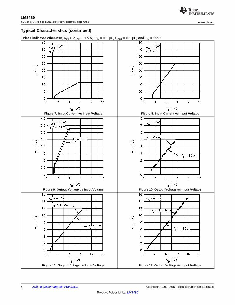
6.7 Typical CharacteristicsUnless indicated otherwise, VIN = VNOM + 1.5 V, CIN = 0.1 µF, COUT = 0.1 µF, and TA .= 25°C.
Figure 1. Dropout Voltage vs Load Current Figure 2. Dropout Voltage vs Junction Temperature
Figure 3. Ground Pin Current vs Input Voltage Figure 4. Ground Pin Current vs Input Voltage
Figure 5. Ground Pin Current vs Load Current Figure 6. Ground Pin Current vs Junction Temperature
Copyright © 1999–2015, Texas Instruments Incorporated Submit Documentation Feedback 7
Product Folder Links: LM3480
LM3480SNVS011H –JUNE 1999–REVISED SEPTEMBER 2015 www.ti.com
Typical Characteristics (continued)Unless indicated otherwise, VIN = VNOM + 1.5 V, CIN = 0.1 µF, COUT = 0.1 µF, and TA .= 25°C.
Figure 7. Input Current vs Input Voltage Figure 8. Input Current vs Input Voltage
Figure 9. Output Voltage vs Input Voltage Figure 10. Output Voltage vs Input Voltage
Figure 11. Output Voltage vs Input Voltage Figure 12. Output Voltage vs Input Voltage
8 Submit Documentation Feedback Copyright © 1999–2015, Texas Instruments Incorporated
Product Folder Links: LM3480

LM3480www.ti.com SNVS011H –JUNE 1999–REVISED SEPTEMBER 2015
Typical Characteristics (continued)Unless indicated otherwise, VIN = VNOM + 1.5 V, CIN = 0.1 µF, COUT = 0.1 µF, and TA .= 25°C.
Figure 13. Output Short-Circuit Current Figure 14. Output Short-Circuit Current
Figure 15. Power Supply Rejection Ratio Figure 16. Power Supply Rejection Ratio
Figure 17. DC Load Regulation
Copyright © 1999–2015, Texas Instruments Incorporated Submit Documentation Feedback 9
Product Folder Links: LM3480

+
Current Limit
IN OUT
GND
LM3480
PNP
BandgapReference
ThermalShutdown
NPN
LM3480SNVS011H –JUNE 1999–REVISED SEPTEMBER 2015 www.ti.com
7 Detailed Description
7.1 OverviewThe LM3480 is an integrated linear voltage regulator with inputs that can be as high as 30 V. It ensures amaximum dropout of 1.2 V at the full load of 100 mA. The LM3480 has different output options including 3.3-V, 5-V, 12-V, and 15-V outputs, making LM3480 the tiny alternative to industry standard LM78Lxx series and similardevices.
7.2 Functional Block Diagram
7.3 Feature Description
7.3.1 3.3-V, 5-V, 12-V, and 15-V Versions AvailableThe 3.3-V, 5-V, 12-V, and 15-V versions of LM3480 series are intended as tiny alternatives to industry standardLM78Lxx series and similar devices.
7.3.2 1.2-V Ensured Maximum DropoutThe 1.2-V quasi-low dropout of the LM3480 series devices make them a nice fit in many application where the 2-V to 2.5-V dropout of LM78Lxx series devices precludes their use.
7.4 Device Functional Modes
7.4.1 Operation with VIN = 5 VThe 3.3-V member of LM3480 can operate with an input of 5 V ±5%, its tiny SOT-23 package and quasi-lowdropout makes it suitable for providing a very tiny, 3.3-V, 100-mA bias supply from 5-V power supply.
10 Submit Documentation Feedback Copyright © 1999–2015, Texas Instruments Incorporated
Product Folder Links: LM3480

COUT
0.1 µF
LM3480IM3-5.0
3
2 15 V, 100 mA OUT6.5 V IN
CIN
0.1 µF
LM3480www.ti.com SNVS011H –JUNE 1999–REVISED SEPTEMBER 2015
8 Application and Implementation
NOTEInformation in the following applications sections is not part of the TI componentspecification, and TI does not warrant its accuracy or completeness. TI’s customers areresponsible for determining suitability of components for their purposes. Customers shouldvalidate and test their design implementation to confirm system functionality.
8.1 Application InformationThe LM3480 is a linear voltage regulator with 1.2-V ensured maximum dropout and 100-mA ensured minimumload current. This device has 3.3-V, 5-V, 12-V, and 15-V versions. The implementation of LM3480 is discussed inthis section.
8.2 Typical Application
8.2.1 Design Requirements
DESIGN PARAMETER EXAMPLE VALUEInput voltage 6.5 V
Output voltage 5 VOutput current 100 mA
8.2.2 Detailed Design Procedure
8.2.2.1 External CapacitorsA minimum input and output capacitance value of 0.1 µF is required for stability and adequate transientperformance. There is no specific ESR limitation, although excessively high ESR will compromise transientperformance. There is no specific limitation on a maximum capacitance value on the input or the output.
8.2.2.1.1 Output Capacitor
The minimum output capacitance required to maintain stability is 0.1 µF. Larger values of output capacitance canbe used to improve transient behavior.
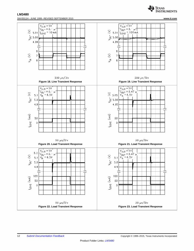
8.2.3 Application CurvesUnless indicated otherwise, VIN = 6.5 V, VOUT = 5 V, COUT = 0.1 µF, and TA = 25°C
Copyright © 1999–2015, Texas Instruments Incorporated Submit Documentation Feedback 11
Product Folder Links: LM3480
LM3480SNVS011H –JUNE 1999–REVISED SEPTEMBER 2015 www.ti.com
Figure 18. Line Transient Response Figure 19. Line Transient Response
Figure 20. Load Transient Response Figure 21. Load Transient Response
Figure 22. Load Transient Response Figure 23. Load Transient Response
12 Submit Documentation Feedback Copyright © 1999–2015, Texas Instruments Incorporated
Product Folder Links: LM3480

VOUTVIN
GND
IN
GND
OUT
2 1
3
LM3480www.ti.com SNVS011H –JUNE 1999–REVISED SEPTEMBER 2015
9 Power Supply RecommendationsThe LM3480 is designed to operated from up to a 30-V input voltage supply. This input supply must be wellregulated. If the input supply is noisy, additional input capacitors with low ESR can help to improve the outputnoise performance.
10 Layout
10.1 Layout GuidelinesFor best overall performance, place all the circuit components on the same side of the circuit board and as nearas practical to the respective LDO pin connections. Place ground return connections to the input and outputcapacitors, and to the LDO ground pin as close to each other as possible, connected by a wide, component-side,copper surface. The use of vias and long traces to create LDO circuit connections is strongly discouraged andnegatively affects system performance. This grounding and layout scheme minimizes the inductive parasitic, andthereby reduces load-current transients, minimizes noise, and increases circuit stability.
A ground reference plane is also recommended and is either embedded in the PCB itself or located on thebottom side of the PCB opposite the components. This reference plane serves to assure accuracy of the outputvoltage, shield noise, and behaves similar to a thermal plane to spread heat from the LDO device. In mostapplications, this ground plane is necessary to meet thermal requirements.
10.2 Layout Example
Copyright © 1999–2015, Texas Instruments Incorporated Submit Documentation Feedback 13
Product Folder Links: LM3480
LM3480SNVS011H –JUNE 1999–REVISED SEPTEMBER 2015 www.ti.com
11 Device and Documentation Support
11.1 Community ResourcesThe following links connect to TI community resources. Linked contents are provided "AS IS" by the respectivecontributors. They do not constitute TI specifications and do not necessarily reflect TI's views; see TI's Terms ofUse.
TI E2E™ Online Community TI's Engineer-to-Engineer (E2E) Community. Created to foster collaborationamong engineers. At e2e.ti.com, you can ask questions, share knowledge, explore ideas and helpsolve problems with fellow engineers.
Design Support TI's Design Support Quickly find helpful E2E forums along with design support tools andcontact information for technical support.
11.2 TrademarksE2E is a trademark of Texas Instruments.All other trademarks are the property of their respective owners.
11.3 Electrostatic Discharge CautionThese devices have limited built-in ESD protection. The leads should be shorted together or the device placed in conductive foamduring storage or handling to prevent electrostatic damage to the MOS gates.
11.4 GlossarySLYZ022 — TI Glossary.
This glossary lists and explains terms, acronyms, and definitions.
12 Mechanical, Packaging, and Orderable InformationThe following pages include mechanical, packaging, and orderable information. This information is the mostcurrent data available for the designated devices. This data is subject to change without notice and revision ofthis document. For browser-based versions of this data sheet, refer to the left-hand navigation.
14 Submit Documentation Feedback Copyright © 1999–2015, Texas Instruments Incorporated
Product Folder Links: LM3480

PACKAGE OPTION ADDENDUM
www.ti.com 14-Oct-2017
Addendum-Page 1
PACKAGING INFORMATION
Orderable Device Status(1)
Package Type PackageDrawing
Pins PackageQty
Eco Plan(2)
Lead/Ball Finish(6)
MSL Peak Temp(3)
Op Temp (°C) Device Marking(4/5)
Samples
LM3480IM3-12 NRND SOT-23 DBZ 3 1000 TBD Call TI Call TI -40 to 125 L0C
LM3480IM3-12/NOPB ACTIVE SOT-23 DBZ 3 1000 Green (RoHS& no Sb/Br)
CU SN Level-1-260C-UNLIM -40 to 125 L0C
LM3480IM3-15/NOPB ACTIVE SOT-23 DBZ 3 1000 Green (RoHS& no Sb/Br)
CU SN Level-1-260C-UNLIM -40 to 125 L0D
LM3480IM3-3.3 NRND SOT-23 DBZ 3 1000 TBD Call TI Call TI -40 to 125 L0A
LM3480IM3-3.3/NOPB ACTIVE SOT-23 DBZ 3 1000 Green (RoHS& no Sb/Br)
CU SN Level-1-260C-UNLIM -40 to 125 L0A
LM3480IM3-5.0 NRND SOT-23 DBZ 3 1000 TBD Call TI Call TI -40 to 125 L0B
LM3480IM3-5.0/NOPB ACTIVE SOT-23 DBZ 3 1000 Green (RoHS& no Sb/Br)
CU SN Level-1-260C-UNLIM -40 to 125 L0B
LM3480IM3X-12/NOPB ACTIVE SOT-23 DBZ 3 3000 Green (RoHS& no Sb/Br)
CU SN Level-1-260C-UNLIM -40 to 125 L0C
LM3480IM3X-15/NOPB ACTIVE SOT-23 DBZ 3 3000 Green (RoHS& no Sb/Br)
CU SN Level-1-260C-UNLIM -40 to 125 L0D
LM3480IM3X-3.3 NRND SOT-23 DBZ 3 3000 TBD Call TI Call TI -40 to 125 L0A
LM3480IM3X-3.3/NOPB ACTIVE SOT-23 DBZ 3 3000 Green (RoHS& no Sb/Br)
CU SN Level-1-260C-UNLIM -40 to 125 L0A
LM3480IM3X-5.0/NOPB ACTIVE SOT-23 DBZ 3 3000 Green (RoHS& no Sb/Br)
CU SN Level-1-260C-UNLIM -40 to 125 L0B
(1) The marketing status values are defined as follows:ACTIVE: Product device recommended for new designs.LIFEBUY: TI has announced that the device will be discontinued, and a lifetime-buy period is in effect.NRND: Not recommended for new designs. Device is in production to support existing customers, but TI does not recommend using this part in a new design.PREVIEW: Device has been announced but is not in production. Samples may or may not be available.OBSOLETE: TI has discontinued the production of the device.
(2) RoHS: TI defines "RoHS" to mean semiconductor products that are compliant with the current EU RoHS requirements for all 10 RoHS substances, including the requirement that RoHS substancedo not exceed 0.1% by weight in homogeneous materials. Where designed to be soldered at high temperatures, "RoHS" products are suitable for use in specified lead-free processes. TI mayreference these types of products as "Pb-Free".RoHS Exempt: TI defines "RoHS Exempt" to mean products that contain lead but are compliant with EU RoHS pursuant to a specific EU RoHS exemption.Green: TI defines "Green" to mean the content of Chlorine (Cl) and Bromine (Br) based flame retardants meet JS709B low halogen requirements of <=1000ppm threshold. Antimony trioxide basedflame retardants must also meet the <=1000ppm threshold requirement.

PACKAGE OPTION ADDENDUM
www.ti.com 14-Oct-2017
Addendum-Page 2
(3) MSL, Peak Temp. - The Moisture Sensitivity Level rating according to the JEDEC industry standard classifications, and peak solder temperature.
(4) There may be additional marking, which relates to the logo, the lot trace code information, or the environmental category on the device.
(5) Multiple Device Markings will be inside parentheses. Only one Device Marking contained in parentheses and separated by a "~" will appear on a device. If a line is indented then it is a continuationof the previous line and the two combined represent the entire Device Marking for that device.
(6) Lead/Ball Finish - Orderable Devices may have multiple material finish options. Finish options are separated by a vertical ruled line. Lead/Ball Finish values may wrap to two lines if the finishvalue exceeds the maximum column width.
Important Information and Disclaimer:The information provided on this page represents TI's knowledge and belief as of the date that it is provided. TI bases its knowledge and belief on informationprovided by third parties, and makes no representation or warranty as to the accuracy of such information. Efforts are underway to better integrate information from third parties. TI has taken andcontinues to take reasonable steps to provide representative and accurate information but may not have conducted destructive testing or chemical analysis on incoming materials and chemicals.TI and TI suppliers consider certain information to be proprietary, and thus CAS numbers and other limited information may not be available for release.
In no event shall TI's liability arising out of such information exceed the total purchase price of the TI part(s) at issue in this document sold by TI to Customer on an annual basis.

TAPE AND REEL INFORMATION
*All dimensions are nominal
Device PackageType
PackageDrawing
Pins SPQ ReelDiameter
(mm)
ReelWidth
W1 (mm)
A0(mm)
B0(mm)
K0(mm)
P1(mm)
W(mm)
Pin1Quadrant
LM3480IM3-12 SOT-23 DBZ 3 1000 178.0 8.4 3.3 2.9 1.22 4.0 8.0 Q3
LM3480IM3-12/NOPB SOT-23 DBZ 3 1000 178.0 8.4 3.3 2.9 1.22 4.0 8.0 Q3
LM3480IM3-15/NOPB SOT-23 DBZ 3 1000 178.0 8.4 3.3 2.9 1.22 4.0 8.0 Q3
LM3480IM3-3.3 SOT-23 DBZ 3 1000 178.0 8.4 3.3 2.9 1.22 4.0 8.0 Q3
LM3480IM3-3.3/NOPB SOT-23 DBZ 3 1000 178.0 8.4 3.3 2.9 1.22 4.0 8.0 Q3
LM3480IM3-5.0 SOT-23 DBZ 3 1000 178.0 8.4 3.3 2.9 1.22 4.0 8.0 Q3
LM3480IM3-5.0/NOPB SOT-23 DBZ 3 1000 178.0 8.4 3.3 2.9 1.22 4.0 8.0 Q3
LM3480IM3X-12/NOPB SOT-23 DBZ 3 3000 178.0 8.4 3.3 2.9 1.22 4.0 8.0 Q3
LM3480IM3X-15/NOPB SOT-23 DBZ 3 3000 178.0 8.4 3.3 2.9 1.22 4.0 8.0 Q3
LM3480IM3X-3.3 SOT-23 DBZ 3 3000 178.0 8.4 3.3 2.9 1.22 4.0 8.0 Q3
LM3480IM3X-3.3/NOPB SOT-23 DBZ 3 3000 178.0 8.4 3.3 2.9 1.22 4.0 8.0 Q3
LM3480IM3X-5.0/NOPB SOT-23 DBZ 3 3000 178.0 8.4 3.3 2.9 1.22 4.0 8.0 Q3
PACKAGE MATERIALS INFORMATION
www.ti.com 24-Aug-2017
Pack Materials-Page 1

*All dimensions are nominal
Device Package Type Package Drawing Pins SPQ Length (mm) Width (mm) Height (mm)
LM3480IM3-12 SOT-23 DBZ 3 1000 210.0 185.0 35.0
LM3480IM3-12/NOPB SOT-23 DBZ 3 1000 210.0 185.0 35.0
LM3480IM3-15/NOPB SOT-23 DBZ 3 1000 210.0 185.0 35.0
LM3480IM3-3.3 SOT-23 DBZ 3 1000 210.0 185.0 35.0
LM3480IM3-3.3/NOPB SOT-23 DBZ 3 1000 210.0 185.0 35.0
LM3480IM3-5.0 SOT-23 DBZ 3 1000 210.0 185.0 35.0
LM3480IM3-5.0/NOPB SOT-23 DBZ 3 1000 210.0 185.0 35.0
LM3480IM3X-12/NOPB SOT-23 DBZ 3 3000 210.0 185.0 35.0
LM3480IM3X-15/NOPB SOT-23 DBZ 3 3000 210.0 185.0 35.0
LM3480IM3X-3.3 SOT-23 DBZ 3 3000 210.0 185.0 35.0
LM3480IM3X-3.3/NOPB SOT-23 DBZ 3 3000 210.0 185.0 35.0
LM3480IM3X-5.0/NOPB SOT-23 DBZ 3 3000 210.0 185.0 35.0
PACKAGE MATERIALS INFORMATION
www.ti.com 24-Aug-2017
Pack Materials-Page 2

4203227/C

www.ti.com
PACKAGE OUTLINE
C
TYP0.200.08
0.25
2.642.10
1.12 MAX
TYP0.100.01
3X 0.50.3
TYP0.60.2
1.9
0.95
TYP-80
A
3.042.80
B1.41.2
(0.95)
SOT-23 - 1.12 mm max heightDBZ0003ASMALL OUTLINE TRANSISTOR
4214838/C 04/2017
NOTES: 1. All linear dimensions are in millimeters. Any dimensions in parenthesis are for reference only. Dimensioning and tolerancing per ASME Y14.5M.2. This drawing is subject to change without notice.3. Reference JEDEC registration TO-236, except minimum foot length.
0.2 C A B
1
3
2
INDEX AREAPIN 1
GAGE PLANE
SEATING PLANE
0.1 C
SCALE 4.000

www.ti.com
EXAMPLE BOARD LAYOUT
0.07 MAXALL AROUND
0.07 MINALL AROUND
3X (1.3)
3X (0.6)
(2.1)
2X (0.95)
(R0.05) TYP
4214838/C 04/2017
SOT-23 - 1.12 mm max heightDBZ0003ASMALL OUTLINE TRANSISTOR
NOTES: (continued) 4. Publication IPC-7351 may have alternate designs. 5. Solder mask tolerances between and around signal pads can vary based on board fabrication site.
SYMM
LAND PATTERN EXAMPLESCALE:15X
PKG
1
3
2
SOLDER MASKOPENINGMETAL UNDER
SOLDER MASK
SOLDER MASKDEFINED
METALSOLDER MASKOPENING
NON SOLDER MASKDEFINED
(PREFERRED)
SOLDER MASK DETAILS

www.ti.com
EXAMPLE STENCIL DESIGN
(2.1)
2X(0.95)
3X (1.3)
3X (0.6)
(R0.05) TYP
SOT-23 - 1.12 mm max heightDBZ0003ASMALL OUTLINE TRANSISTOR
4214838/C 04/2017
NOTES: (continued) 6. Laser cutting apertures with trapezoidal walls and rounded corners may offer better paste release. IPC-7525 may have alternate design recommendations. 7. Board assembly site may have different recommendations for stencil design.
SOLDER PASTE EXAMPLEBASED ON 0.125 THICK STENCIL
SCALE:15X
SYMM
PKG
1
3
2
IMPORTANT NOTICE
Texas Instruments Incorporated (TI) reserves the right to make corrections, enhancements, improvements and other changes to itssemiconductor products and services per JESD46, latest issue, and to discontinue any product or service per JESD48, latest issue. Buyersshould obtain the latest relevant information before placing orders and should verify that such information is current and complete.TI’s published terms of sale for semiconductor products (http://www.ti.com/sc/docs/stdterms.htm) apply to the sale of packaged integratedcircuit products that TI has qualified and released to market. Additional terms may apply to the use or sale of other types of TI products andservices.Reproduction of significant portions of TI information in TI data sheets is permissible only if reproduction is without alteration and isaccompanied by all associated warranties, conditions, limitations, and notices. TI is not responsible or liable for such reproduceddocumentation. Information of third parties may be subject to additional restrictions. Resale of TI products or services with statementsdifferent from or beyond the parameters stated by TI for that product or service voids all express and any implied warranties for theassociated TI product or service and is an unfair and deceptive business practice. TI is not responsible or liable for any such statements.Buyers and others who are developing systems that incorporate TI products (collectively, “Designers”) understand and agree that Designersremain responsible for using their independent analysis, evaluation and judgment in designing their applications and that Designers havefull and exclusive responsibility to assure the safety of Designers' applications and compliance of their applications (and of all TI productsused in or for Designers’ applications) with all applicable regulations, laws and other applicable requirements. Designer represents that, withrespect to their applications, Designer has all the necessary expertise to create and implement safeguards that (1) anticipate dangerousconsequences of failures, (2) monitor failures and their consequences, and (3) lessen the likelihood of failures that might cause harm andtake appropriate actions. Designer agrees that prior to using or distributing any applications that include TI products, Designer willthoroughly test such applications and the functionality of such TI products as used in such applications.TI’s provision of technical, application or other design advice, quality characterization, reliability data or other services or information,including, but not limited to, reference designs and materials relating to evaluation modules, (collectively, “TI Resources”) are intended toassist designers who are developing applications that incorporate TI products; by downloading, accessing or using TI Resources in anyway, Designer (individually or, if Designer is acting on behalf of a company, Designer’s company) agrees to use any particular TI Resourcesolely for this purpose and subject to the terms of this Notice.TI’s provision of TI Resources does not expand or otherwise alter TI’s applicable published warranties or warranty disclaimers for TIproducts, and no additional obligations or liabilities arise from TI providing such TI Resources. TI reserves the right to make corrections,enhancements, improvements and other changes to its TI Resources. TI has not conducted any testing other than that specificallydescribed in the published documentation for a particular TI Resource.Designer is authorized to use, copy and modify any individual TI Resource only in connection with the development of applications thatinclude the TI product(s) identified in such TI Resource. NO OTHER LICENSE, EXPRESS OR IMPLIED, BY ESTOPPEL OR OTHERWISETO ANY OTHER TI INTELLECTUAL PROPERTY RIGHT, AND NO LICENSE TO ANY TECHNOLOGY OR INTELLECTUAL PROPERTYRIGHT OF TI OR ANY THIRD PARTY IS GRANTED HEREIN, including but not limited to any patent right, copyright, mask work right, orother intellectual property right relating to any combination, machine, or process in which TI products or services are used. Informationregarding or referencing third-party products or services does not constitute a license to use such products or services, or a warranty orendorsement thereof. Use of TI Resources may require a license from a third party under the patents or other intellectual property of thethird party, or a license from TI under the patents or other intellectual property of TI.TI RESOURCES ARE PROVIDED “AS IS” AND WITH ALL FAULTS. TI DISCLAIMS ALL OTHER WARRANTIES ORREPRESENTATIONS, EXPRESS OR IMPLIED, REGARDING RESOURCES OR USE THEREOF, INCLUDING BUT NOT LIMITED TOACCURACY OR COMPLETENESS, TITLE, ANY EPIDEMIC FAILURE WARRANTY AND ANY IMPLIED WARRANTIES OFMERCHANTABILITY, FITNESS FOR A PARTICULAR PURPOSE, AND NON-INFRINGEMENT OF ANY THIRD PARTY INTELLECTUALPROPERTY RIGHTS. TI SHALL NOT BE LIABLE FOR AND SHALL NOT DEFEND OR INDEMNIFY DESIGNER AGAINST ANY CLAIM,INCLUDING BUT NOT LIMITED TO ANY INFRINGEMENT CLAIM THAT RELATES TO OR IS BASED ON ANY COMBINATION OFPRODUCTS EVEN IF DESCRIBED IN TI RESOURCES OR OTHERWISE. IN NO EVENT SHALL TI BE LIABLE FOR ANY ACTUAL,DIRECT, SPECIAL, COLLATERAL, INDIRECT, PUNITIVE, INCIDENTAL, CONSEQUENTIAL OR EXEMPLARY DAMAGES INCONNECTION WITH OR ARISING OUT OF TI RESOURCES OR USE THEREOF, AND REGARDLESS OF WHETHER TI HAS BEENADVISED OF THE POSSIBILITY OF SUCH DAMAGES.Unless TI has explicitly designated an individual product as meeting the requirements of a particular industry standard (e.g., ISO/TS 16949and ISO 26262), TI is not responsible for any failure to meet such industry standard requirements.Where TI specifically promotes products as facilitating functional safety or as compliant with industry functional safety standards, suchproducts are intended to help enable customers to design and create their own applications that meet applicable functional safety standardsand requirements. Using products in an application does not by itself establish any safety features in the application. Designers mustensure compliance with safety-related requirements and standards applicable to their applications. Designer may not use any TI products inlife-critical medical equipment unless authorized officers of the parties have executed a special contract specifically governing such use.Life-critical medical equipment is medical equipment where failure of such equipment would cause serious bodily injury or death (e.g., lifesupport, pacemakers, defibrillators, heart pumps, neurostimulators, and implantables). Such equipment includes, without limitation, allmedical devices identified by the U.S. Food and Drug Administration as Class III devices and equivalent classifications outside the U.S.TI may expressly designate certain products as completing a particular qualification (e.g., Q100, Military Grade, or Enhanced Product).Designers agree that it has the necessary expertise to select the product with the appropriate qualification designation for their applicationsand that proper product selection is at Designers’ own risk. Designers are solely responsible for compliance with all legal and regulatoryrequirements in connection with such selection.Designer will fully indemnify TI and its representatives against any damages, costs, losses, and/or liabilities arising out of Designer’s non-compliance with the terms and provisions of this Notice.
Mailing Address: Texas Instruments, Post Office Box 655303, Dallas, Texas 75265Copyright © 2017, Texas Instruments Incorporated