lp3869x/-q1 500-ma low-dropout cmos linear regulators ... · lp38691, lp38693, lp38691-q1,...
TRANSCRIPT

LP38693
IN OUT
SNS**
GND1 µF * 1 µF *
VOUTVIN
VENEN
LP38691
IN OUT
SNS**
GND1 µF * 1 µF *
VOUTVIN
Product
Folder
Sample &Buy
Technical
Documents
Tools &
Software
Support &Community
ReferenceDesign
LP38691, LP38693, LP38691-Q1, LP38693-Q1SNVS321O –JANUARY 2005–REVISED DECEMBER 2015
LP3869x/-Q1 500-mA Low-Dropout CMOS Linear RegulatorsStable With Ceramic Output Capacitors
1 Features 3 DescriptionThe LP3869x low-dropout CMOS linear regulators
1• Wide Input Voltage Range (2.7 V to 10 V)provide tight output tolerance (2% typical), extremely• All WSON Options are Available as AEC-Q100 low dropout voltage (250 mV at 500-mA load current,
Grade 1 VOUT = 5 V), and excellent AC performance using• 2% Output Accuracy (25°C) ultralow equivalent series resistance (ESR) ceramic
output capacitors.• Low Dropout Voltage: 250 mV at 500 mA (Typical,5 V Out) The low thermal resistance of the WSON, SOT-223,
and TO-252 packages allow use of the full operating• Precision (Trimmed) Bandgap Referencecurrent even in high ambient temperature• Ensured Specifications for –40°C to 125°Cenvironments.
• 1-µA Off-State Quiescent CurrentThe use of a PMOS power transistor means that no• Thermal Overload Protection DC base-drive current is required to bias it, thus
• Foldback Current Limiting allowing ground pin current to remain below 100 µA• Ground Pin Current: 55 µA (typical) at full load regardless of load current, input voltage, or operating
temperature.• Enable Pin (LP38693)
Device Information(1)2 Applications
PART NUMBER PACKAGE BODY SIZE (NOM)• Hard Disk Drives TO-252 (3) 6.58 mm × 6.10 mm
LP38691• Notebook Computers WSON (6) 3.00 mm × 3.00 mm• Battery-Powered Devices SOT-223 (5) 6.50 mm × 3.56 mm
LP38693• Portable Instrumentation WSON (6) 3.00 mm × 3.00 mmLP38691-Q1
WSON (6) 3.00 mm × 3.00 mmLP38693-Q1
(1) For all available packages, see the orderable addendum atthe end of the data sheet.
4 Typical Application Circuits
* Minimum value required for stability* Minimum value required for stability** WSON package devices only** WSON package devices only
1
An IMPORTANT NOTICE at the end of this data sheet addresses availability, warranty, changes, use in safety-critical applications,intellectual property matters and other important disclaimers. PRODUCTION DATA.
LP38691, LP38693, LP38691-Q1, LP38693-Q1SNVS321O –JANUARY 2005–REVISED DECEMBER 2015 www.ti.com
Table of Contents8.4 Device Functional Modes........................................ 131 Features .................................................................. 1
9 Application and Implementation ........................ 142 Applications ........................................................... 19.1 Application Information............................................ 143 Description ............................................................. 19.2 Typical Application ................................................. 144 Typical Application Circuits ................................. 1
10 Power Supply Recommendations ..................... 195 Revision History..................................................... 211 Layout................................................................... 196 Pin Configuration and Functions ......................... 3
11.1 Layout Guidelines ................................................. 197 Specifications......................................................... 411.2 Layout Example .................................................... 197.1 Absolute Maximum Ratings ...................................... 411.3 WSON Mounting ................................................... 207.2 ESD Ratings: LP38691 and LP38693....................... 4
12 Device and Documentation Support ................. 217.3 ESD Ratings: LP38691-Q1 and LP38693-Q1........... 412.1 Documentation Support ........................................ 217.4 Recommended Operating Conditions....................... 412.2 Related Links ........................................................ 217.5 Thermal Information .................................................. 512.3 Community Resources.......................................... 217.6 Electrical Characteristics........................................... 512.4 Trademarks ........................................................... 217.7 Typical Characteristics .............................................. 712.5 Electrostatic Discharge Caution............................ 218 Detailed Description ............................................ 1112.6 Glossary ................................................................ 218.1 Overview ................................................................. 11
13 Mechanical, Packaging, and Orderable8.2 Functional Block Diagrams ..................................... 11Information ........................................................... 218.3 Feature Description................................................. 13
5 Revision HistoryNOTE: Page numbers for previous revisions may differ from page numbers in the current version.
Changes from Revision N (March 2015) to Revision O Page
• Added top navigator icon for TI Designs ............................................................................................................................... 1• Added Caution note to Foldback Current Limiting subsection ............................................................................................ 13
Changes from Revision M (February 2015) to Revision N Page
• Added "Cout = xx pF" to "Cout = µF" for Figures 4 through 6 in Typical Characteristics ...................................................... 1
Changes from Revision L (December 2014) to Revision M Page
• Changed wording of Description and added one item to Features; update Vin, Vout and Ven pin names to IN, OUT,and EN in text and graphics .................................................................................................................................................. 1
• Added top navigator icon for TI Designs ............................................................................................................................... 1• Changed "PFM" to 'TO-252" .................................................................................................................................................. 4• Changed Handling Ratings to ESD Ratings format ............................................................................................................... 4
Changes from Revision K (April 2013) to Revision L Page
• Added Handling Rating table, Feature Description section, Device Functional Modes, Application andImplementation section, Power Supply Recommendations section, Layout section, Device and DocumentationSupport section, and Mechanical, Packaging, and Orderable Information section; update thermal values .......................... 1
Changes from Revision J (April 2013) to Revision K Page
• Changed layout of National Data Sheet to TI format ........................................................................................................... 18
2 Submit Documentation Feedback Copyright © 2005–2015, Texas Instruments Incorporated
Product Folder Links: LP38691 LP38693 LP38691-Q1 LP38693-Q1
IN
2
3 4
5
61
GND
EN OUT
SNS
IN
Exposed Pad
on Bottom
(DAP)
IN
2
3 4
5
61
GND
N/C OUT
SNS
IN
Exposed Pad
on Bottom
(DAP)
N/C
OUT
GND
EN
IN
1
2
4
3
5
LP38691, LP38693, LP38691-Q1, LP38693-Q1www.ti.com SNVS321O –JANUARY 2005–REVISED DECEMBER 2015
6 Pin Configuration and Functions
NDP Package3-Pin TO-252
Top View
NDC Package5-Pin SOT-223
Top View
NC - No internal connection
NGG Package6-Pin WSON With Exposed Thermal Pad
LP38691SD Top View
NC - No internal connection
NGG Package6-Pin WSON With Exposed Thermal Pad
LP38693SD Top View
Copyright © 2005–2015, Texas Instruments Incorporated Submit Documentation Feedback 3
Product Folder Links: LP38691 LP38693 LP38691-Q1 LP38693-Q1
LP38691, LP38693, LP38691-Q1, LP38693-Q1SNVS321O –JANUARY 2005–REVISED DECEMBER 2015 www.ti.com
Pin FunctionsPIN
I/O DESCRIPTIONTO- SOT-NAME WSON252 223WSON Only - The DAP (Exposed Pad) functions as a thermal connection whenDAP — √ √ — — soldered to a copper plane. See WSON Mounting section for more information.The EN pin allows the part to be turned ON and OFF by pulling this pin high orEN — — 3 1 I low.Circuit ground for the regulator. For the TO-252 and SOT-223 packages this is
GND TAB 2 2 5 — thermally connected to the die and functions as a heat sink when the soldereddown to a large copper plane.This is the input supply voltage to the regulator. For WSON devices, both ININ 3 1, 6 1, 6 4 I pins must be tied together for full current operation (250 mA maximum per pin).
OUT 1 4 4 3 O Regulated output voltageWSON Only - Output SNS pin allows remote sensing at the load which eliminate
SNS — 5 5 — I the error in output voltage due to voltage drops caused by the resistance in thetraces between the regulator and the load. This pin must be tied to OUT.
7 Specifications
7.1 Absolute Maximum Ratings (1) (2)
MIN MAX UNITLead temp. (Soldering, 5 seconds) 260 °CPower dissipation (3) Internally Limited VV(max) All pins (with respect to GND) –0.3 12 VIOUT
(4) Internally Limited VJunction temperature –40 150
°CStorage temperature, Tstg −65 150
(1) Absolute maximum ratings indicate limits beyond which damage to the component may occur. Operating ratings indicate conditions forwhich the device is intended to be functional, but do not ensure specific performance limits. For ensured specifications, see ElectricalCharacteristics. Specifications do not apply when operating the device outside of its rated operating conditions.
(2) If Military/Aerospace specified devices are required, contact the Texas Instruments Sales Office/ Distributors for availability andspecifications.
(3) At elevated temperatures, device power dissipation must be derated based on package thermal resistance and heatsink values (if aheatsink is used). When using the WSON package, refer to AN-1187 Leadless Leadframe Package (LLP), SNOA401, and the WSONMounting section in this datasheet. If power dissipation causes the junction temperature to exceed specified limits, the device goes intothermal shutdown.
(4) If used in a dual-supply system where the regulator load is returned to a negative supply, the output pin must be diode clamped toground.
7.2 ESD Ratings: LP38691 and LP38693VALUE UNIT
V(ESD) Electrostatic discharge Human-body model (HBM), per ANSI/ESDA/JEDEC JS-001 (1) ±2000 V
(1) JEDEC document JEP155 states that 500-V HBM allows safe manufacturing with a standard ESD control process.
7.3 ESD Ratings: LP38691-Q1 and LP38693-Q1VALUE UNIT
V(ESD) Electrostatic discharge Human-body model (HBM), per AEC Q100-002 (1) ±2000 V
(1) AEC Q100-002 indicates that HBM stressing shall be in accordance with the ANSI/ESDA/JEDEC JS-001 specification.
7.4 Recommended Operating ConditionsMIN NOM MAX UNIT
VIN supply voltage 2.7 10 VOperating junction temperature −40 125 °C
4 Submit Documentation Feedback Copyright © 2005–2015, Texas Instruments Incorporated
Product Folder Links: LP38691 LP38693 LP38691-Q1 LP38693-Q1

LP38691, LP38693, LP38691-Q1, LP38693-Q1www.ti.com SNVS321O –JANUARY 2005–REVISED DECEMBER 2015
7.5 Thermal InformationLP38691 LP38693 LP3869x
THERMAL METRIC (1) TO-252 WSON SOT-223 UNIT3 PINS 6 PINS 5 PINS
RθJA(2) Junction-to-ambient thermal resistance 50.5 50.6 68.5 °C/W
RθJC(top) Junction-to-case (top) thermal resistance 52.6 44.4 52.2 °C/WRθJB Junction-to-board thermal resistance 29.7 24.9 13.0 °C/WψJT Junction-to-top characterization parameter 4.8 0.4 5.5 °C/WψJB Junction-to-board characterization parameter 29.3 25.1 12.8 °C/WRθJC(bot) Junction-to-case (bottom) thermal resistance 1.5 5.4 n/a °C/W
(1) For more information about traditional and new thermal metrics, see the Semiconductor and IC Package Thermal Metrics applicationreport, SPRA953.
(2) Junction-to-ambient thermal resistance, High-K.
7.6 Electrical CharacteristicsUnless otherwise specified, limits apply for TJ = 25°C, VIN = VOUT + 1 V, CIN = COUT = 10 µF, ILOAD = 10 mA. Minimum andmaximum limits are specified through testing, statistical correlation, or design.
PARAMETER TEST CONDITIONS MIN TYP (1) MAX UNIT–2 2
100 µA < IL < 0.5 AVO Output voltage tolerance %VOUTVO + 1 V ≤ VIN ≤ 10 V –4 4Full operating temperature rangeVO + 0.5 V ≤ VIN ≤ 10 V 0.03IL = 25 mA
Output voltage lineΔVO/ΔVIN %/VVO + 0.5 V ≤ VIN ≤ 10 Vregulation (2)IL = 25 mA 0.1Full operating temperature range1 mA < IL < 0.5 A 1.8VIN = VO + 1 V
Output voltage loadΔVO/ΔIL %/A1 mA < IL < 0.5 Aregulation (3)VIN = VO + 1 V 5Full operating temperature range
IL = 0.1 A 80(VO = 2.5 V)
IL = 0.5 A 430(VO = 2.5 V) IL = 0.1 A 145Full operating temperature IL = 0.5 A 725range
IL = 0.1 A 65(VO = 3.3 V)
IL = 0.5 A 330VIN – VOUT Dropout voltage (4) mV(VO = 3.3 V) IL = 0.1 A 110
Full operating temperature IL = 0.5 A 550rangeIL = 0.1 A 45
(VO = 5 V)IL = 0.5 A 250
(VO = 5 V) IL = 0.1 A 100Full operating temperature IL = 0.5 A 450range
(1) Typical numbers represent the most likely parametric norm for 25°C operation.(2) Output voltage line regulation is defined as the change in output voltage from nominal value resulting from a change in input voltage.(3) Output voltage load regulation is defined as the change in output voltage from nominal value as the load current increases from 1 mA to
full load.(4) Dropout voltage is defined as the minimum input to output differential required to maintain the output within 100 mV of nominal value.
Copyright © 2005–2015, Texas Instruments Incorporated Submit Documentation Feedback 5
Product Folder Links: LP38691 LP38693 LP38691-Q1 LP38693-Q1
LP38691, LP38693, LP38691-Q1, LP38693-Q1SNVS321O –JANUARY 2005–REVISED DECEMBER 2015 www.ti.com
Electrical Characteristics (continued)Unless otherwise specified, limits apply for TJ = 25°C, VIN = VOUT + 1 V, CIN = COUT = 10 µF, ILOAD = 10 mA. Minimum andmaximum limits are specified through testing, statistical correlation, or design.
PARAMETER TEST CONDITIONS MIN TYP (1) MAX UNITVIN ≤ 10 V, IL =100 µA - 0.5 A 55VIN ≤ 10 V, IL =100 µA - 0.5 AIQ Quiescent current 100Full operating temperature range
µAVEN ≤ 0.4 V, (LP38693 Only) 0.001 1VIN – VO ≤ 4 VIL(MIN) Minimum load current 100Full operating temperature rangeVIN – VO > 5 V 350
IFB Foldback current limit mAVIN – VO < 4 V 850
PSRR Ripple rejection VIN = VO + 2 V(DC), with 1 V(p-p) / 120-Hz Ripple 55 dBThermal shutdown activationTSD 160(junction temp)
°CTSD Thermal shutdown hysteresis 10(HYST) (junction temp)
BW = 10 Hz to 10 kHzen Output noise 0.7 µV/√HzVO = 3.3 VVO (LEAK) Output leakage current VO = VO(NOM) + 1 V at 10 VIN 0.5 12 µA
Output = OFF 0.4Full operating temperature rangeOutput = ON, VIN = 4 V 1.8Full operating temperature rangeEnable voltage (LP38693VEN VOnly) Output = ON, VIN = 6 V 3Full operating temperature rangeOutput = ON, VIN = 10 V 4Full operating temperature range
Enable pin leakage VEN = 0 V or 10 V, VIN = 10 VIEN –1 0.001 1 µA(lLP38693 only)
6 Submit Documentation Feedback Copyright © 2005–2015, Texas Instruments Incorporated
Product Folder Links: LP38691 LP38693 LP38691-Q1 LP38693-Q1

10 100 1k 10k 100k
0
10
20
30
40
50
60
FREQUENCY (Hz)
RIP
PLE
RE
JEC
TIO
N (
dB)
COUT = 100 PF
VIN(DC) = 5.3V
VIN(AC) = 1V(p-p)
VOUT = 3.3V
10 100 1k 10k 100k
0
10
20
30
40
50
60
FREQUENCY (Hz)
RIP
PLE
RE
JEC
TIO
N (
dB)
COUT = 1 PF
VIN(DC) = 5.3V
VIN(AC) = 1V(p-p)
VOUT = 3.3V
10 100 1k 10k 100k
0
10
20
30
40
50
60
FREQUENCY (Hz)
RIP
PLE
RE
JEC
TIO
N (
dB
)
COUT = 10 PF
VIN(DC) = 5.3V
VIN(AC) = 1V(p-p)
VOUT = 3.3V
LP38691, LP38693, LP38691-Q1, LP38693-Q1www.ti.com SNVS321O –JANUARY 2005–REVISED DECEMBER 2015
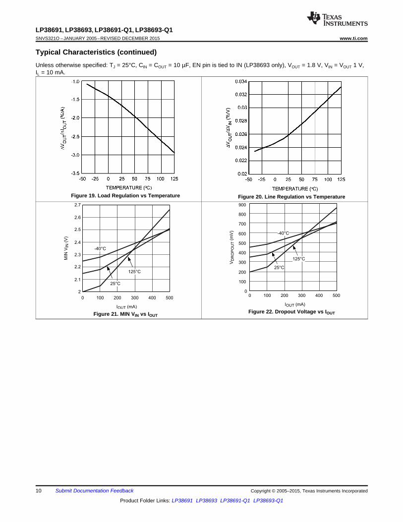
7.7 Typical CharacteristicsUnless otherwise specified: TJ = 25°C, CIN = COUT = 10 µF, EN pin is tied to IN (LP38693 only), VOUT = 1.8 V, VIN = VOUT 1 V,IL = 10 mA.
Figure 2. Noise vs FrequencyFigure 1. Noise vs Frequency
Figure 3. Noise vs Frequency Figure 4. Ripple Rejection
Figure 5. Ripple Rejection Figure 6. Ripple Rejection
Copyright © 2005–2015, Texas Instruments Incorporated Submit Documentation Feedback 7
Product Folder Links: LP38691 LP38693 LP38691-Q1 LP38693-Q1

20
10
0
-10
-20
'V
OU
T (
mV
)
3
4
5
VIN
(V
)VIN
VOUT
VOUT = 3.3V
COUT = 100 PF
200 Ps/DIV
LP38691, LP38693, LP38691-Q1, LP38693-Q1SNVS321O –JANUARY 2005–REVISED DECEMBER 2015 www.ti.com
Typical Characteristics (continued)Unless otherwise specified: TJ = 25°C, CIN = COUT = 10 µF, EN pin is tied to IN (LP38693 only), VOUT = 1.8 V, VIN = VOUT 1 V,IL = 10 mA.
Figure 7. Line Transient Response Figure 8. Line Transient Response
Figure 9. Line Transient Response Figure 10. Load Transient Response
Figure 12. VOUT vs Temperature (5.0 V)Figure 11. Load Transient Response
8 Submit Documentation Feedback Copyright © 2005–2015, Texas Instruments Incorporated
Product Folder Links: LP38691 LP38693 LP38691-Q1 LP38693-Q1

LP38691, LP38693, LP38691-Q1, LP38693-Q1www.ti.com SNVS321O –JANUARY 2005–REVISED DECEMBER 2015
Typical Characteristics (continued)Unless otherwise specified: TJ = 25°C, CIN = COUT = 10 µF, EN pin is tied to IN (LP38693 only), VOUT = 1.8 V, VIN = VOUT 1 V,IL = 10 mA.
Figure 14. VOUT vs Temperature (2.5 V)Figure 13. VOUT vs Temperature (3.3 V)
Figure 15. VOUT vs Temperature (1.8 V) Figure 16. VOUT vs VIN (1.8 V)
Figure 18. Enable Voltage vs TemperatureFigure 17. VOUT vs VIN, Power-Up
Copyright © 2005–2015, Texas Instruments Incorporated Submit Documentation Feedback 9
Product Folder Links: LP38691 LP38693 LP38691-Q1 LP38693-Q1
0 100 200 300 400 500
2
2.1
2.2
2.3
2.4
2.5
2.6
2.7
MIN
VIN
(V)
IOUT (mA)
-40°C
25°C
125°C
0 100 200 300 400 500
IOUT (mA)
0
100
200
300
400
500
600
700
800
900
VD
RO
PO
UT
(mV
)-40°C
25°C
125°C
LP38691, LP38693, LP38691-Q1, LP38693-Q1SNVS321O –JANUARY 2005–REVISED DECEMBER 2015 www.ti.com
Typical Characteristics (continued)Unless otherwise specified: TJ = 25°C, CIN = COUT = 10 µF, EN pin is tied to IN (LP38693 only), VOUT = 1.8 V, VIN = VOUT 1 V,IL = 10 mA.
Figure 19. Load Regulation vs Temperature Figure 20. Line Regulation vs Temperature
Figure 22. Dropout Voltage vs IOUTFigure 21. MIN VIN vs IOUT
10 Submit Documentation Feedback Copyright © 2005–2015, Texas Instruments Incorporated
Product Folder Links: LP38691 LP38693 LP38691-Q1 LP38693-Q1
ENABLE LOGIC
-
+
MOSFETDRIVER
FOLDBACKCURRENTLIMITING
1.25-VREFERENCE
THERMALSHUTDOWN
IN
OUT
GND
P-FET
P-FET
R1
R2
ENABLE LOGIC
-
+
MOSFETDRIVER
FOLDBACKCURRENTLIMITING
1.25-VREFERENCE
THERMALSHUTDOWN
IN
OUT
GND
P-FET
P-FET
N/C
R1
R2
SNS
LP38691, LP38693, LP38691-Q1, LP38693-Q1www.ti.com SNVS321O –JANUARY 2005–REVISED DECEMBER 2015
8 Detailed Description
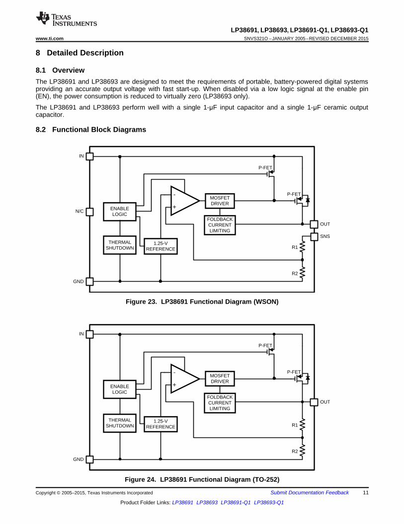
8.1 OverviewThe LP38691 and LP38693 are designed to meet the requirements of portable, battery-powered digital systemsproviding an accurate output voltage with fast start-up. When disabled via a low logic signal at the enable pin(EN), the power consumption is reduced to virtually zero (LP38693 only).
The LP38691 and LP38693 perform well with a single 1-μF input capacitor and a single 1-μF ceramic outputcapacitor.
8.2 Functional Block Diagrams
Figure 23. LP38691 Functional Diagram (WSON)
Figure 24. LP38691 Functional Diagram (TO-252)
Copyright © 2005–2015, Texas Instruments Incorporated Submit Documentation Feedback 11
Product Folder Links: LP38691 LP38693 LP38691-Q1 LP38693-Q1

ENABLE LOGIC
-
+
MOSFETDRIVER
FOLDBACKCURRENTLIMITING
1.25-VREFERENCE
THERMALSHUTDOWN
IN
OUT
GND
P-FET
P-FET
EN
R1
R2
ENABLE LOGIC
-
+
MOSFETDRIVER
FOLDBACKCURRENTLIMITING
1.25-VREFERENCE
THERMALSHUTDOWN
IN
OUT
GND
P-FET
P-FET
EN
R1
R2
SNS
LP38691, LP38693, LP38691-Q1, LP38693-Q1SNVS321O –JANUARY 2005–REVISED DECEMBER 2015 www.ti.com
Functional Block Diagrams (continued)
Figure 25. LP38693 Functional Diagram (WSON)
Figure 26. LP38693 Functional Diagram (SOT-223)
12 Submit Documentation Feedback Copyright © 2005–2015, Texas Instruments Incorporated
Product Folder Links: LP38691 LP38693 LP38691-Q1 LP38693-Q1
LP38691, LP38693, LP38691-Q1, LP38693-Q1www.ti.com SNVS321O –JANUARY 2005–REVISED DECEMBER 2015
8.3 Feature Description
8.3.1 Enable (EN)The LP38693 has an Enable pin (EN) which allows an external control signal to turn the regulator output On andOff. The Enable On/Off threshold has no hysteresis. The voltage signal must rise and fall cleanly, and promptly,through the ON and OFF voltage thresholds. The EN pin voltage must be higher than the VEN(MIN) threshold toensure that the device is fully enabled under all operating conditions. The EN pin voltage must be lower than theVEN(MAX) threshold to ensure that the device is fully disabled. The EN pin has no internal pullup or pulldown toestablish a default condition and, as a result, this pin must be terminated either actively or passively. If the ENpin is driven from a source that actively pulls high and low, the drive voltage must not be allowed to go belowground potential or higher than VIN. If the application does not require the Enable function, the pin must beconnected directly to the IN pin.
8.3.2 Thermal Overload Protection (TSD)Thermal Shutdown disables the output when the junction temperature rises to approximately 160°C which allowsthe device to cool. When the junction temperature cools to approximately 150°C, the output circuitry enables.
Based on power dissipation, thermal resistance, and ambient temperature, the thermal protection circuit maycycle on and off. This thermal cycling limits the dissipation of the regulator and protects it from damage as aresult of overheating. The Thermal Shutdown circuitry of the LP38693 has been designed to protect againsttemporary thermal overload conditions.
The Thermal Shutdown circuitry was not intended to replace proper heat-sinking. Continuously running theLP38693 device into thermal shutdown degrades device reliability.
8.3.3 Foldback Current LimitingFoldback current limiting is built into the LP38691 and LP38693 devices which reduces the amount of outputcurrent the part can deliver as the output voltage is reduced. The amount of load current is dependent on thedifferential voltage between the IN and OUT pins. Typically, when this differential voltage exceeds 5 V, the loadcurrent limits at about 350 mA. When the VIN – VOUT differential is reduced below 4 V, load current is limited toabout 850 mA.
CAUTIONWhen toggling the LP38693 Enable (EN) after the input voltage (VIN) is applied, thefoldback current limit circuitry is functional the first time that the EN pin is taken high.The foldback current limit circuitry is non-functional the second, and subsequent, timesthat the EN pin is taken high. Depending on the input and output capacitance valuesthe input inrush current may be higher than expected which can cause the inputvoltage to droop.
If the EN pin is connected to the IN pin, the foldback current limit circuitry is functionalwhen VIN is applied if VIN starts from less than 0.4 V.
8.4 Device Functional Modes
8.4.1 Enable (EN)The EN pin voltage must be higher than the VEN(MIN) threshold to ensure that the device is fully enabled under alloperating conditions.
8.4.2 Minimum Operating Input Voltage (VIN)The LP38691 and LP38693 do not include any dedicated UVLO circuitry. Neither device internal circuitry is fullyfunctional until VIN is at least 2.7 V. The output voltage is not regulated until VIN ≥ (VOUT + VDO), or 2.7 V,whichever is higher.
Copyright © 2005–2015, Texas Instruments Incorporated Submit Documentation Feedback 13
Product Folder Links: LP38691 LP38693 LP38691-Q1 LP38693-Q1

LP38691
IN OUT
SNS**
GND1 µF * 1 µF *
VOUTVIN
LP38693
IN OUT
SNS**
GND1 µF * 1 µF *
VOUTVIN
VENEN
LP38691, LP38693, LP38691-Q1, LP38693-Q1SNVS321O –JANUARY 2005–REVISED DECEMBER 2015 www.ti.com
9 Application and Implementation
NOTEInformation in the following applications sections is not part of the TI componentspecification, and TI does not warrant its accuracy or completeness. TI’s customers areresponsible for determining suitability of components for their purposes. Customers shouldvalidate and test their design implementation to confirm system functionality.
9.1 Application Information
9.1.1 Reverse VoltageA reverse voltage condition exists when the voltage at the output pin is higher than the voltage at the input pin.Typically this happens when VIN is abruptly taken low and COUT continues to hold a sufficient charge such thatthe input to output voltage becomes reversed. A less common condition is when an alternate voltage source isconnected to the output.
There are two possible paths for current to flow from the OUT pin back to IN during a reverse voltage condition.1. While VIN is high enough to keep the control circuity alive, and the EN pin (LP38693 only) is above the
VEN(ON) threshold, the control circuitry attempts to regulate the output voltage. If the input voltage is less thanthe programmed output voltage, the control circuit drives the gate of the pass element to the full ONcondition. In this condition, reverse current flows from the OUT to the IN pin, limited only by the RDS(ON) ofthe pass element and the output to input voltage differential. Discharging an output capacitor up to 1000 μFin this manner does not damage the device as the current rapidly decays. However, continuous reversecurrent must be avoided. When the EN pin is low, this condition is prevented.
2. The internal PFET pass element has an inherent parasitic diode. During normal operation, the input voltageis higher than the output voltage and the parasitic diode is reverse biased. However, when VIN is below thevalue where the control circuity is alive, or the EN pin is low (LP38693 only), and the output voltage is morethan 500 mV (typical) above the input voltage the parasitic diode becomes forward biased and current flowsfrom the output pin to the input pin through the diode. The current in the parasitic diode must be limited toless than 1-A continuous and 5-A peak.If used in a dual-supply system where the regulator output load is returned to a negative supply, the outputpin must be diode-clamped to ground to limit the negative voltage transition. A Schottky diode isrecommended for this protective clamp.
9.2 Typical Application
* Minimum value required for stability.**WSON package devices only.
14 Submit Documentation Feedback Copyright © 2005–2015, Texas Instruments Incorporated
Product Folder Links: LP38691 LP38693 LP38691-Q1 LP38693-Q1
LP38691, LP38693, LP38691-Q1, LP38693-Q1www.ti.com SNVS321O –JANUARY 2005–REVISED DECEMBER 2015
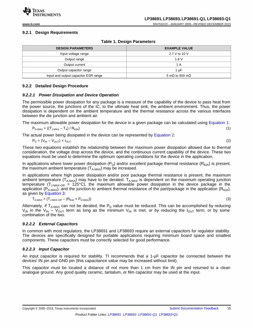
9.2.1 Design Requirements
Table 1. Design ParametersDESIGN PARAMETERS EXAMPLE VALUE
Input voltage range 2.7 V to 10 VOutput range 1.8 VOutput current 1 A
Output capacitor range 1 µFInput and output capacitor ESR range 5 mΩ to 500 mΩ
9.2.2 Detailed Design Procedure
9.2.2.1 Power Dissipation and Device OperationThe permissible power dissipation for any package is a measure of the capability of the device to pass heat fromthe power source, the junctions of the IC, to the ultimate heat sink, the ambient environment. Thus, the powerdissipation is dependent on the ambient temperature and the thermal resistance across the various interfacesbetween the die junction and ambient air.
The maximum allowable power dissipation for the device in a given package can be calculated using Equation 1:PD-MAX = ((TJ-MAX – TA) / RθJA) (1)
The actual power being dissipated in the device can be represented by Equation 2:PD = (VIN – VOUT) × IOUT (2)
These two equations establish the relationship between the maximum power dissipation allowed due to thermalconsideration, the voltage drop across the device, and the continuous current capability of the device. These twoequations must be used to determine the optimum operating conditions for the device in the application.
In applications where lower power dissipation (PD) and/or excellent package thermal resistance (RθJA) is present,the maximum ambient temperature (TA-MAX) may be increased.
In applications where high power dissipation and/or poor package thermal resistance is present, the maximumambient temperature (TA-MAX) may have to be derated. TA-MAX is dependent on the maximum operating junctiontemperature (TJ-MAX-OP = 125°C), the maximum allowable power dissipation in the device package in theapplication (PD-MAX), and the junction-to ambient thermal resistance of the part/package in the application (RθJA),as given by Equation 3:
TA-MAX = (TJ-MAX-OP – (RθJA × PD-MAX)) (3)
Alternately, if TA-MAX can not be derated, the PD value must be reduced. This can be accomplished by reducingVIN in the VIN – VOUT term as long as the minimum VIN is met, or by reducing the IOUT term, or by somecombination of the two.
9.2.2.2 External CapacitorsIn common with most regulators, the LP38691 and LP38693 require an external capacitors for regulator stability.The devices are specifically designed for portable applications requiring minimum board space and smallestcomponents. These capacitors must be correctly selected for good performance.
9.2.2.3 Input CapacitorAn input capacitor is required for stability. TI recommends that a 1-µF capacitor be connected between thedevices' IN pin and GND pin (this capacitance value may be increased without limit).
This capacitor must be located a distance of not more than 1 cm from the IN pin and returned to a cleananalogue ground. Any good quality ceramic, tantalum, or film capacitor may be used at the input.
Copyright © 2005–2015, Texas Instruments Incorporated Submit Documentation Feedback 15
Product Folder Links: LP38691 LP38693 LP38691-Q1 LP38693-Q1
LP38691, LP38693, LP38691-Q1, LP38693-Q1SNVS321O –JANUARY 2005–REVISED DECEMBER 2015 www.ti.com
Important: To ensure stable operation it is essential that good PCB design practices are employed to minimizeground impedance and keep input inductance low. If these conditions cannot be met, or if long leads are used toconnect the battery or other power source to the LP38691 or LP38693, then TI recommends that the inputcapacitor is increased. Also, tantalum capacitors can suffer catastrophic failures due to surge current whenconnected to a low-impedance source of power (like a battery or a very large capacitor). If a tantalum capacitor isused at the input, it must be ensured by the manufacturer to have a surge current rating sufficient for theapplication.
There are no requirements for the equivalent series resistance (ESR) on the input capacitor, but tolerance andtemperature coefficient must be considered when selecting the capacitor to ensure the capacitance remainsapproximately 1 µF over the entire operating temperature range.
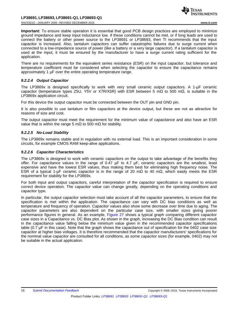
9.2.2.4 Output CapacitorThe LP3869x is designed specifically to work with very small ceramic output capacitors. A 1-µF ceramiccapacitor (temperature types Z5U, Y5V or X7R/X5R) with ESR between 5 mΩ to 500 mΩ, is suitable in theLP3869x application circuit.
For this device the output capacitor must be connected between the OUT pin and GND pin.
It is also possible to use tantalum or film capacitors at the device output, but these are not as attractive forreasons of size and cost.
The output capacitor must meet the requirement for the minimum value of capacitance and also have an ESRvalue that is within the range 5 mΩ to 500 mΩ for stability.
9.2.2.5 No-Load StabilityThe LP3869x remains stable and in regulation with no external load. This is an important consideration in somecircuits, for example CMOS RAM keep-alive applications.
9.2.2.6 Capacitor CharacteristicsThe LP3869x is designed to work with ceramic capacitors on the output to take advantage of the benefits theyoffer. For capacitance values in the range of 0.47 µF to 4.7 µF, ceramic capacitors are the smallest, leastexpensive and have the lowest ESR values, thus making them best for eliminating high frequency noise. TheESR of a typical 1-µF ceramic capacitor is in the range of 20 mΩ to 40 mΩ, which easily meets the ESRrequirement for stability for the LP3869x.
For both input and output capacitors, careful interpretation of the capacitor specification is required to ensurecorrect device operation. The capacitor value can change greatly, depending on the operating conditions andcapacitor type.
In particular, the output capacitor selection must take account of all the capacitor parameters, to ensure that thespecification is met within the application. The capacitance can vary with DC bias conditions as well astemperature and frequency of operation. Capacitor values also show some decrease over time due to aging. Thecapacitor parameters are also dependent on the particular case size, with smaller sizes giving poorerperformance figures in general. As an example, Figure 27 shows a typical graph comparing different capacitorcase sizes in a Capacitance vs. DC Bias plot. As shown in the graph, increasing the DC Bias condition can resultin the capacitance value falling below the minimum value given in the recommended capacitor specificationstable (0.7 µF in this case). Note that the graph shows the capacitance out of specification for the 0402 case sizecapacitor at higher bias voltages. It is therefore recommended that the capacitor manufacturers’ specifications forthe nominal value capacitor are consulted for all conditions, as some capacitor sizes (for example, 0402) may notbe suitable in the actual application.
16 Submit Documentation Feedback Copyright © 2005–2015, Texas Instruments Incorporated
Product Folder Links: LP38691 LP38693 LP38691-Q1 LP38693-Q1

0402, 6.3V, X5R
0603, 10V, X5R
0 1.0 2.0 3.0 4.0 5.0
DC BIAS (V)
20%
40%
60%
80%
100%
CA
P V
ALU
E (
% o
f NO
MIN
AL
1 P
F)
LP38691, LP38693, LP38691-Q1, LP38693-Q1www.ti.com SNVS321O –JANUARY 2005–REVISED DECEMBER 2015
Figure 27. Typical Variation In Capacitance vs DC Bias
The value of the ceramic capacitor can vary with temperature. The capacitor type X7R, which operates over atemperature range of –55°C to 125°C, only varies the capacitance to within ±15%. The capacitor type X5R has asimilar tolerance over a reduced temperature range of –55°C to 85°C. Many large value ceramic capacitors,larger than 1 µF, are manufactured with Z5U or Y5V temperature characteristics. Their capacitance can drop bymore than 50% as the temperature varies from 25°C to 85°C. Therefore, X7R and X5R types are recommendedover Z5U and Y5V in applications where the ambient temperature changes significantly above or below 25°C.
Tantalum capacitors are less desirable than ceramic for use as output capacitors because they are more costlywhen comparing equivalent capacitance and voltage ratings in the 0.47-µF to 4.7-µF range.
Another important consideration is that tantalum capacitors have higher ESR values than equivalent sizeceramics. This means that while it may be possible to find a tantalum capacitor with an ESR value within thestable range, it would have to be larger in capacitance (which means bigger and more costly) than a ceramiccapacitor with the same ESR value. It mustalso be noted that the ESR of a typical tantalum increases about 2:1as the temperature goes from 25°C down to –40°C, so some guard band must be allowed.
9.2.2.7 RFI/EMI SusceptibilityRadio frequency interference (RFI) and electromagnetic interference (EMI) can degrade any integrated circuit’sperformance because of the small dimensions of the geometries inside the device. In applications where circuitsources are present which generate signals with significant high frequency energy content (> 1 MHz), care mustbe taken to ensure that this does not affect the device regulator.
If RFI/EMI noise is present on the input side of the regulator (such as applications where the input source comesfrom the output of a switching regulator), good ceramic bypass capacitors must be used at the input pin of thedevice.
If a load is connected to the device output which switches at high speed (such as a clock), the high-frequencycurrent pulses required by the load must be supplied by the capacitors on the IC output. Because the bandwidthof the regulator loop is less than 100 kHz, the control circuitry cannot respond to load changes above thatfrequency. This means the effective output impedance of the device at frequencies above 100 kHz is determinedonly by the output capacitors.
In applications where the load is switching at high speed, the output of the IC may need RF isolation from theload. TI recommends that some inductance be placed between the output capacitor and the load, and good RFbypass capacitors be placed directly across the load.
PCB layout is also critical in high noise environments, because RFI/EMI is easily radiated directly into PC traces.Noisy circuitry must be isolated from clean circuits where possible, and grounded through a separate path. AtMHz frequencies, ground planes begin to look inductive and RFI/ EMI can cause ground bounce across theground plane. In multi-layer PCB applications, care must be taken in layout so that noisy power and groundplanes do not radiate directly into adjacent layers which carry analog power and ground.
Copyright © 2005–2015, Texas Instruments Incorporated Submit Documentation Feedback 17
Product Folder Links: LP38691 LP38693 LP38691-Q1 LP38693-Q1

LP38691, LP38693, LP38691-Q1, LP38693-Q1SNVS321O –JANUARY 2005–REVISED DECEMBER 2015 www.ti.com
9.2.2.8 Output NoiseNoise is specified in two ways: Spot Noise or Output Noise Density is the RMS sum of all noise sources,measured at the regulator output, at a specific frequency (measured with a 1-Hz bandwidth). This type of noise isusually plotted on a curve as a function of frequency. Total Output Noise or Broad-Band Noise is the RMS sumof spot noise over a specified bandwidth, usually several decades of frequencies.
Attention paid to the units of measurement. Spot noise is measured in units µV√Hz or nV√Hz, and total outputnoise is measured in µVRMS.
The primary source of noise in low-dropout regulators is the internal reference. Noise can be reduced in twoways: by increasing the transistor area or by increasing the current drawn by the internal reference. Increasingthe area decreases the chance of fitting the die into a smaller package. Increasing the current drawn by theinternal reference increases the total supply current (GND pin current).
9.2.3 Application Curves
Figure 28. VOUT vs VEN, ON (LP38693 Only) Figure 29. VOUT vs VEN, OFF (LP38693 Only)
18 Submit Documentation Feedback Copyright © 2005–2015, Texas Instruments Incorporated
Product Folder Links: LP38691 LP38693 LP38691-Q1 LP38693-Q1
COUT
VOUT
CIN
LP38691DT
Power Ground
VININ
OUT
GN
D
VIN
CIN
COUT
SNS
OUT
LP38691SD
Power
Ground
1
2
3 4
5
6
Thermal
Pad
N/C
IN IN
LP38691, LP38693, LP38691-Q1, LP38693-Q1www.ti.com SNVS321O –JANUARY 2005–REVISED DECEMBER 2015
10 Power Supply RecommendationsThe LP38691 and LP38693 are designed to operate from an input supply voltage range of 2.7 V to 10 V. Theinput supply must be well regulated and free of spurious noise. To ensure that the device output voltage is wellregulated, input supply must be at least VOUT + 0.5 V, or 2.7 V, whichever is higher. A minimum capacitor valueof 1-μF is required to be within 1 cm of the IN pin.
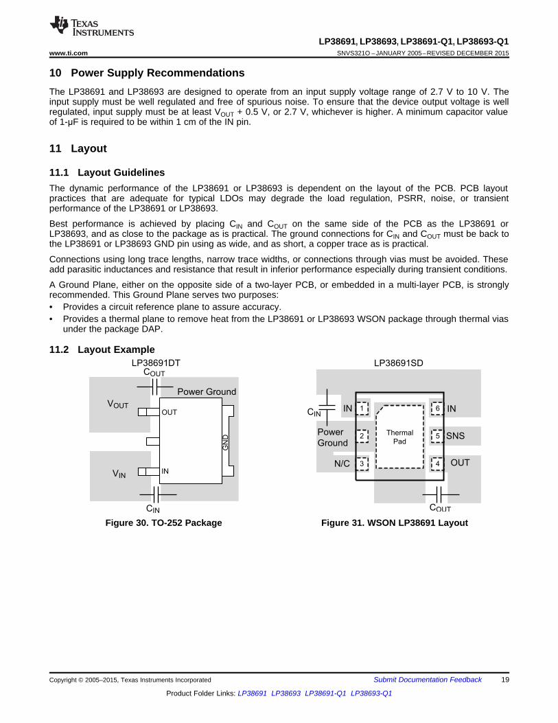
11 Layout
11.1 Layout GuidelinesThe dynamic performance of the LP38691 or LP38693 is dependent on the layout of the PCB. PCB layoutpractices that are adequate for typical LDOs may degrade the load regulation, PSRR, noise, or transientperformance of the LP38691 or LP38693.
Best performance is achieved by placing CIN and COUT on the same side of the PCB as the LP38691 orLP38693, and as close to the package as is practical. The ground connections for CIN and COUT must be back tothe LP38691 or LP38693 GND pin using as wide, and as short, a copper trace as is practical.
Connections using long trace lengths, narrow trace widths, or connections through vias must be avoided. Theseadd parasitic inductances and resistance that result in inferior performance especially during transient conditions.
A Ground Plane, either on the opposite side of a two-layer PCB, or embedded in a multi-layer PCB, is stronglyrecommended. This Ground Plane serves two purposes:• Provides a circuit reference plane to assure accuracy.• Provides a thermal plane to remove heat from the LP38691 or LP38693 WSON package through thermal vias
under the package DAP.
11.2 Layout Example
Figure 30. TO-252 Package Figure 31. WSON LP38691 Layout
space
space
Copyright © 2005–2015, Texas Instruments Incorporated Submit Documentation Feedback 19
Product Folder Links: LP38691 LP38693 LP38691-Q1 LP38693-Q1

COUT
SNS
OUT
CIN
LP38693SD
Power
Ground
1
2
3 4
5
6
Thermal
Pad
EN
IN INCOUT
VOUT
CIN
LP38693MP
Power
GroundVIN
EN
NC
OUT
IN
GND
LP38691, LP38693, LP38691-Q1, LP38693-Q1SNVS321O –JANUARY 2005–REVISED DECEMBER 2015 www.ti.com
Layout Example (continued)
Figure 32. SOT-223 Layout Figure 33. WSON LP38693 Layout
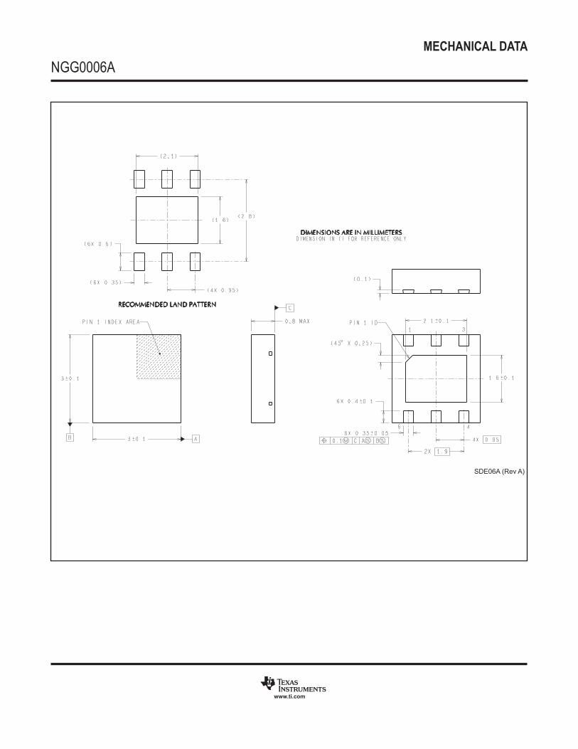
11.3 WSON MountingThe NGG0006A (No Pullback) 6-Lead WSON package requires specific mounting techniques which are detailedin the TI AN-1187 Application Report SNOA401. Referring to the section PCB Design Recommendations, notethat the pad style which must be used with the WSON package is the NSMD (non-solder mask defined) type.Additionally, TI recommends the PCB terminal pads to be 0.2 mm longer than the package pads to create asolder fillet to improve reliability and inspection.
The input current is split between two IN pins, 1 and 6. The two IN pins must be connected together to ensurethat the device can meet all specifications at the rated current.
The thermal dissipation of the WSON package is directly related to the printed circuit board construction and theamount of additional copper area connected to the DAP.
The DAP (exposed pad) on the bottom of the WSON package is connected to the die substrate with a conductivedie attach adhesive. The DAP has no direct electrical (wire) connection to any of the pins. There is a parasitic PNjunction between the die substrate and the device ground. As such, it is strongly recommend that the DAP beconnected directly to the ground at device lead 2 (that is, GND). Alternately, but not recommended, the DAP maybe left floating (that is, no electrical connection). The DAP must not be connected to any potential other thanground.
20 Submit Documentation Feedback Copyright © 2005–2015, Texas Instruments Incorporated
Product Folder Links: LP38691 LP38693 LP38691-Q1 LP38693-Q1
LP38691, LP38693, LP38691-Q1, LP38693-Q1www.ti.com SNVS321O –JANUARY 2005–REVISED DECEMBER 2015
12 Device and Documentation Support
12.1 Documentation Support
12.1.1 Related DocumentationFor related documentation see the following:
Texas Instruments AN-1187 Leadless Leadframe Package (LLP) (SNOA401).
12.2 Related LinksThe table below lists quick access links. Categories include technical documents, support and communityresources, tools and software, and quick access to sample or buy.
Table 2. Related LinksTECHNICAL TOOLS & SUPPORT &PARTS PRODUCT FOLDER SAMPLE & BUY DOCUMENTS SOFTWARE COMMUNITY
LP38691 Click here Click here Click here Click here Click hereLP38693 Click here Click here Click here Click here Click here
LP38691-Q1 Click here Click here Click here Click here Click hereLP38693-Q1 Click here Click here Click here Click here Click here
12.3 Community ResourcesThe following links connect to TI community resources. Linked contents are provided "AS IS" by the respectivecontributors. They do not constitute TI specifications and do not necessarily reflect TI's views; see TI's Terms ofUse.
TI E2E™ Online Community TI's Engineer-to-Engineer (E2E) Community. Created to foster collaborationamong engineers. At e2e.ti.com, you can ask questions, share knowledge, explore ideas and helpsolve problems with fellow engineers.
Design Support TI's Design Support Quickly find helpful E2E forums along with design support tools andcontact information for technical support.
12.4 TrademarksE2E is a trademark of Texas Instruments.All other trademarks are the property of their respective owners.
12.5 Electrostatic Discharge CautionThese devices have limited built-in ESD protection. The leads should be shorted together or the device placed in conductive foamduring storage or handling to prevent electrostatic damage to the MOS gates.
12.6 GlossarySLYZ022 — TI Glossary.
This glossary lists and explains terms, acronyms, and definitions.
13 Mechanical, Packaging, and Orderable InformationThe following pages include mechanical, packaging, and orderable information. This information is the mostcurrent data available for the designated devices. This data is subject to change without notice and revision ofthis document. For browser-based versions of this data sheet, refer to the left-hand navigation.
Copyright © 2005–2015, Texas Instruments Incorporated Submit Documentation Feedback 21
Product Folder Links: LP38691 LP38693 LP38691-Q1 LP38693-Q1

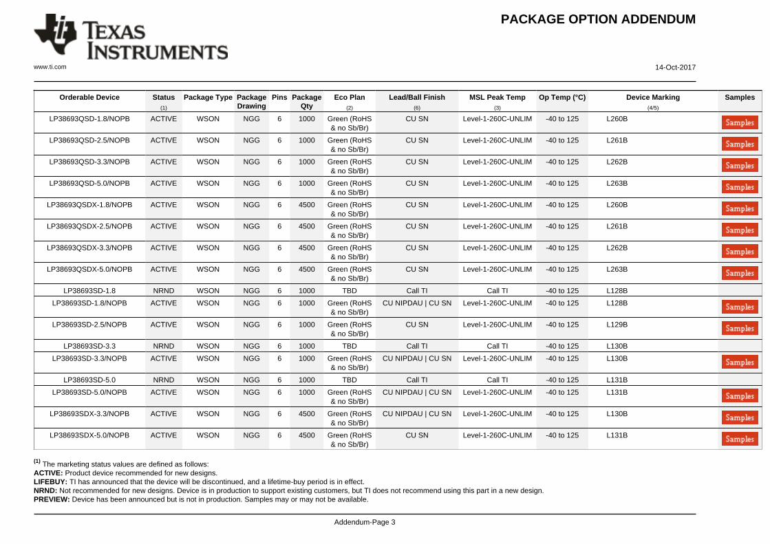
PACKAGE OPTION ADDENDUM
www.ti.com 14-Oct-2017
Addendum-Page 1
PACKAGING INFORMATION
Orderable Device Status(1)
Package Type PackageDrawing
Pins PackageQty
Eco Plan(2)
Lead/Ball Finish(6)
MSL Peak Temp(3)
Op Temp (°C) Device Marking(4/5)
Samples
LP38691DT-1.8 NRND TO-252 NDP 3 75 TBD Call TI Call TI -40 to 125 LP38691DT-1.8
LP38691DT-1.8/NOPB ACTIVE TO-252 NDP 3 75 Green (RoHS& no Sb/Br)
CU SN Level-2-260C-1 YEAR -40 to 125 LP38691DT-1.8
LP38691DT-2.5/NOPB ACTIVE TO-252 NDP 3 75 Green (RoHS& no Sb/Br)
CU SN Level-2-260C-1 YEAR -40 to 125 LP38691DT-2.5
LP38691DT-3.3 NRND TO-252 NDP 3 75 TBD Call TI Call TI -40 to 125 LP38691DT-3.3
LP38691DT-3.3/NOPB ACTIVE TO-252 NDP 3 75 Green (RoHS& no Sb/Br)
CU SN Level-2-260C-1 YEAR -40 to 125 LP38691DT-3.3
LP38691DT-5.0/NOPB ACTIVE TO-252 NDP 3 75 Green (RoHS& no Sb/Br)
CU SN Level-2-260C-1 YEAR -40 to 125 LP38691DT-5.0
LP38691DTX-1.8/NOPB ACTIVE TO-252 NDP 3 2500 Green (RoHS& no Sb/Br)
CU SN Level-2-260C-1 YEAR -40 to 125 LP38691DT-1.8
LP38691DTX-2.5/NOPB ACTIVE TO-252 NDP 3 2500 Green (RoHS& no Sb/Br)
CU SN Level-2-260C-1 YEAR -40 to 125 LP38691DT-2.5
LP38691DTX-3.3/NOPB ACTIVE TO-252 NDP 3 2500 Green (RoHS& no Sb/Br)
CU SN Level-2-260C-1 YEAR -40 to 125 LP38691DT-3.3
LP38691DTX-5.0/NOPB ACTIVE TO-252 NDP 3 2500 Green (RoHS& no Sb/Br)
CU SN Level-2-260C-1 YEAR -40 to 125 LP38691DT-5.0
LP38691QSD-1.8/NOPB ACTIVE WSON NGG 6 1000 Green (RoHS& no Sb/Br)
CU SN Level-1-260C-UNLIM -40 to 125 L256B
LP38691QSD-2.5/NOPB ACTIVE WSON NGG 6 1000 Green (RoHS& no Sb/Br)
CU SN Level-1-260C-UNLIM -40 to 125 L257B
LP38691QSD-3.3/NOPB ACTIVE WSON NGG 6 1000 Green (RoHS& no Sb/Br)
CU SN Level-1-260C-UNLIM -40 to 125 L258B
LP38691QSD-5.0/NOPB ACTIVE WSON NGG 6 1000 Green (RoHS& no Sb/Br)
CU SN Level-1-260C-UNLIM -40 to 125 L259B
LP38691QSDX-1.8/NOPB ACTIVE WSON NGG 6 4500 Green (RoHS& no Sb/Br)
CU SN Level-1-260C-UNLIM -40 to 125 L256B
LP38691QSDX-2.5/NOPB ACTIVE WSON NGG 6 4500 Green (RoHS& no Sb/Br)
CU SN Level-1-260C-UNLIM -40 to 125 L257B
LP38691QSDX-3.3/NOPB ACTIVE WSON NGG 6 4500 Green (RoHS& no Sb/Br)
CU SN Level-1-260C-UNLIM -40 to 125 L258B
PACKAGE OPTION ADDENDUM
www.ti.com 14-Oct-2017
Addendum-Page 2
Orderable Device Status(1)
Package Type PackageDrawing
Pins PackageQty
Eco Plan(2)
Lead/Ball Finish(6)
MSL Peak Temp(3)
Op Temp (°C) Device Marking(4/5)
Samples
LP38691QSDX-5.0/NOPB ACTIVE WSON NGG 6 4500 Green (RoHS& no Sb/Br)
CU SN Level-1-260C-UNLIM -40 to 125 L259B
LP38691SD-1.8/NOPB ACTIVE WSON NGG 6 1000 Green (RoHS& no Sb/Br)
CU NIPDAU | CU SN Level-1-260C-UNLIM -40 to 125 L118B
LP38691SD-2.5/NOPB ACTIVE WSON NGG 6 1000 Green (RoHS& no Sb/Br)
CU NIPDAU | CU SN Level-1-260C-UNLIM -40 to 125 L119B
LP38691SD-3.3/NOPB ACTIVE WSON NGG 6 1000 Green (RoHS& no Sb/Br)
CU NIPDAU | CU SN Level-1-260C-UNLIM -40 to 125 L120B
LP38691SD-5.0/NOPB ACTIVE WSON NGG 6 1000 Green (RoHS& no Sb/Br)
CU NIPDAU | CU SN Level-1-260C-UNLIM -40 to 125 L121B
LP38691SDX-1.8/NOPB ACTIVE WSON NGG 6 4500 Green (RoHS& no Sb/Br)
CU NIPDAU | CU SN Level-1-260C-UNLIM -40 to 125 L118B
LP38691SDX-2.5/NOPB ACTIVE WSON NGG 6 4500 Green (RoHS& no Sb/Br)
CU SN Level-1-260C-UNLIM -40 to 125 L119B
LP38691SDX-3.3/NOPB ACTIVE WSON NGG 6 4500 Green (RoHS& no Sb/Br)
CU SN Level-1-260C-UNLIM -40 to 125 L120B
LP38691SDX-5.0/NOPB ACTIVE WSON NGG 6 4500 Green (RoHS& no Sb/Br)
CU NIPDAU | CU SN Level-1-260C-UNLIM -40 to 125 L121B
LP38693MP-1.8/NOPB ACTIVE SOT-223 NDC 5 1000 Green (RoHS& no Sb/Br)
CU SN Level-1-260C-UNLIM -40 to 125 LJVB
LP38693MP-2.5/NOPB ACTIVE SOT-223 NDC 5 1000 Green (RoHS& no Sb/Br)
CU SN Level-1-260C-UNLIM -40 to 125 LJXB
LP38693MP-3.3 NRND SOT-223 NDC 5 1000 TBD Call TI Call TI -40 to 125 LJYB
LP38693MP-3.3/NOPB ACTIVE SOT-223 NDC 5 1000 Green (RoHS& no Sb/Br)
CU SN Level-1-260C-UNLIM -40 to 125 LJYB
LP38693MP-5.0/NOPB ACTIVE SOT-223 NDC 5 1000 Green (RoHS& no Sb/Br)
CU SN Level-1-260C-UNLIM -40 to 125 LJZB
LP38693MPX-1.8/NOPB ACTIVE SOT-223 NDC 5 2000 Green (RoHS& no Sb/Br)
CU SN Level-1-260C-UNLIM -40 to 125 LJVB
LP38693MPX-2.5/NOPB ACTIVE SOT-223 NDC 5 2000 Green (RoHS& no Sb/Br)
CU SN Level-1-260C-UNLIM -40 to 125 LJXB
LP38693MPX-3.3/NOPB ACTIVE SOT-223 NDC 5 2000 Green (RoHS& no Sb/Br)
CU SN Level-1-260C-UNLIM -40 to 125 LJYB
LP38693MPX-5.0/NOPB ACTIVE SOT-223 NDC 5 2000 Green (RoHS& no Sb/Br)
CU SN Level-1-260C-UNLIM -40 to 125 LJZB
PACKAGE OPTION ADDENDUM
www.ti.com 14-Oct-2017
Addendum-Page 3
Orderable Device Status(1)
Package Type PackageDrawing
Pins PackageQty
Eco Plan(2)
Lead/Ball Finish(6)
MSL Peak Temp(3)
Op Temp (°C) Device Marking(4/5)
Samples
LP38693QSD-1.8/NOPB ACTIVE WSON NGG 6 1000 Green (RoHS& no Sb/Br)
CU SN Level-1-260C-UNLIM -40 to 125 L260B
LP38693QSD-2.5/NOPB ACTIVE WSON NGG 6 1000 Green (RoHS& no Sb/Br)
CU SN Level-1-260C-UNLIM -40 to 125 L261B
LP38693QSD-3.3/NOPB ACTIVE WSON NGG 6 1000 Green (RoHS& no Sb/Br)
CU SN Level-1-260C-UNLIM -40 to 125 L262B
LP38693QSD-5.0/NOPB ACTIVE WSON NGG 6 1000 Green (RoHS& no Sb/Br)
CU SN Level-1-260C-UNLIM -40 to 125 L263B
LP38693QSDX-1.8/NOPB ACTIVE WSON NGG 6 4500 Green (RoHS& no Sb/Br)
CU SN Level-1-260C-UNLIM -40 to 125 L260B
LP38693QSDX-2.5/NOPB ACTIVE WSON NGG 6 4500 Green (RoHS& no Sb/Br)
CU SN Level-1-260C-UNLIM -40 to 125 L261B
LP38693QSDX-3.3/NOPB ACTIVE WSON NGG 6 4500 Green (RoHS& no Sb/Br)
CU SN Level-1-260C-UNLIM -40 to 125 L262B
LP38693QSDX-5.0/NOPB ACTIVE WSON NGG 6 4500 Green (RoHS& no Sb/Br)
CU SN Level-1-260C-UNLIM -40 to 125 L263B
LP38693SD-1.8 NRND WSON NGG 6 1000 TBD Call TI Call TI -40 to 125 L128B
LP38693SD-1.8/NOPB ACTIVE WSON NGG 6 1000 Green (RoHS& no Sb/Br)
CU NIPDAU | CU SN Level-1-260C-UNLIM -40 to 125 L128B
LP38693SD-2.5/NOPB ACTIVE WSON NGG 6 1000 Green (RoHS& no Sb/Br)
CU SN Level-1-260C-UNLIM -40 to 125 L129B
LP38693SD-3.3 NRND WSON NGG 6 1000 TBD Call TI Call TI -40 to 125 L130B
LP38693SD-3.3/NOPB ACTIVE WSON NGG 6 1000 Green (RoHS& no Sb/Br)
CU NIPDAU | CU SN Level-1-260C-UNLIM -40 to 125 L130B
LP38693SD-5.0 NRND WSON NGG 6 1000 TBD Call TI Call TI -40 to 125 L131B
LP38693SD-5.0/NOPB ACTIVE WSON NGG 6 1000 Green (RoHS& no Sb/Br)
CU NIPDAU | CU SN Level-1-260C-UNLIM -40 to 125 L131B
LP38693SDX-3.3/NOPB ACTIVE WSON NGG 6 4500 Green (RoHS& no Sb/Br)
CU NIPDAU | CU SN Level-1-260C-UNLIM -40 to 125 L130B
LP38693SDX-5.0/NOPB ACTIVE WSON NGG 6 4500 Green (RoHS& no Sb/Br)
CU SN Level-1-260C-UNLIM -40 to 125 L131B
(1) The marketing status values are defined as follows:ACTIVE: Product device recommended for new designs.LIFEBUY: TI has announced that the device will be discontinued, and a lifetime-buy period is in effect.NRND: Not recommended for new designs. Device is in production to support existing customers, but TI does not recommend using this part in a new design.PREVIEW: Device has been announced but is not in production. Samples may or may not be available.

PACKAGE OPTION ADDENDUM
www.ti.com 14-Oct-2017
Addendum-Page 4
OBSOLETE: TI has discontinued the production of the device.
(2) RoHS: TI defines "RoHS" to mean semiconductor products that are compliant with the current EU RoHS requirements for all 10 RoHS substances, including the requirement that RoHS substancedo not exceed 0.1% by weight in homogeneous materials. Where designed to be soldered at high temperatures, "RoHS" products are suitable for use in specified lead-free processes. TI mayreference these types of products as "Pb-Free".RoHS Exempt: TI defines "RoHS Exempt" to mean products that contain lead but are compliant with EU RoHS pursuant to a specific EU RoHS exemption.Green: TI defines "Green" to mean the content of Chlorine (Cl) and Bromine (Br) based flame retardants meet JS709B low halogen requirements of <=1000ppm threshold. Antimony trioxide basedflame retardants must also meet the <=1000ppm threshold requirement.
(3) MSL, Peak Temp. - The Moisture Sensitivity Level rating according to the JEDEC industry standard classifications, and peak solder temperature.
(4) There may be additional marking, which relates to the logo, the lot trace code information, or the environmental category on the device.
(5) Multiple Device Markings will be inside parentheses. Only one Device Marking contained in parentheses and separated by a "~" will appear on a device. If a line is indented then it is a continuationof the previous line and the two combined represent the entire Device Marking for that device.
(6) Lead/Ball Finish - Orderable Devices may have multiple material finish options. Finish options are separated by a vertical ruled line. Lead/Ball Finish values may wrap to two lines if the finishvalue exceeds the maximum column width.
Important Information and Disclaimer:The information provided on this page represents TI's knowledge and belief as of the date that it is provided. TI bases its knowledge and belief on informationprovided by third parties, and makes no representation or warranty as to the accuracy of such information. Efforts are underway to better integrate information from third parties. TI has taken andcontinues to take reasonable steps to provide representative and accurate information but may not have conducted destructive testing or chemical analysis on incoming materials and chemicals.TI and TI suppliers consider certain information to be proprietary, and thus CAS numbers and other limited information may not be available for release.
In no event shall TI's liability arising out of such information exceed the total purchase price of the TI part(s) at issue in this document sold by TI to Customer on an annual basis.
OTHER QUALIFIED VERSIONS OF LP38691, LP38691-Q1, LP38693, LP38693-Q1 :
• Catalog: LP38691, LP38693
• Automotive: LP38691-Q1, LP38693-Q1
NOTE: Qualified Version Definitions:
• Catalog - TI's standard catalog product
• Automotive - Q100 devices qualified for high-reliability automotive applications targeting zero defects

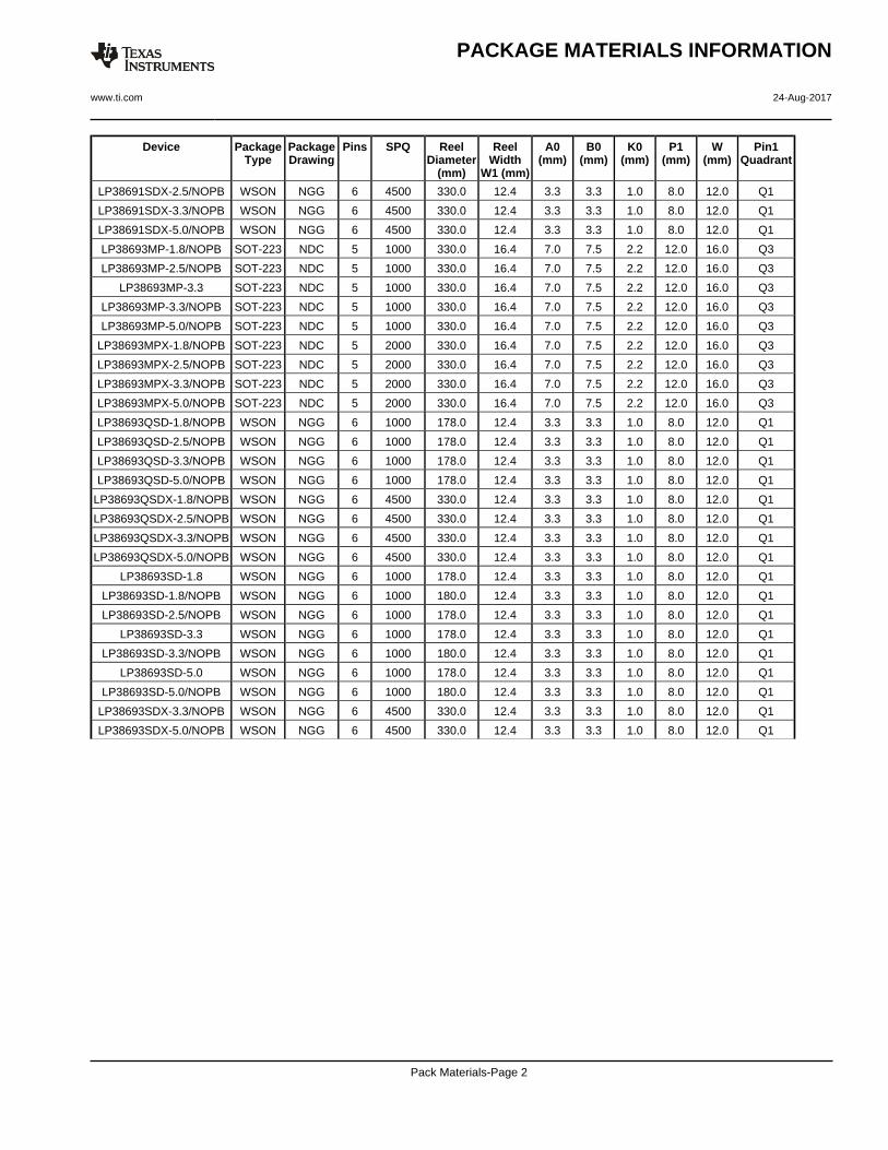
TAPE AND REEL INFORMATION
*All dimensions are nominal
Device PackageType
PackageDrawing
Pins SPQ ReelDiameter
(mm)
ReelWidth
W1 (mm)
A0(mm)
B0(mm)
K0(mm)
P1(mm)
W(mm)
Pin1Quadrant
LP38691DTX-1.8/NOPB TO-252 NDP 3 2500 330.0 16.4 6.9 10.5 2.7 8.0 16.0 Q2
LP38691DTX-2.5/NOPB TO-252 NDP 3 2500 330.0 16.4 6.9 10.5 2.7 8.0 16.0 Q2
LP38691DTX-3.3/NOPB TO-252 NDP 3 2500 330.0 16.4 6.9 10.5 2.7 8.0 16.0 Q2
LP38691DTX-5.0/NOPB TO-252 NDP 3 2500 330.0 16.4 6.9 10.5 2.7 8.0 16.0 Q2
LP38691QSD-1.8/NOPB WSON NGG 6 1000 178.0 12.4 3.3 3.3 1.0 8.0 12.0 Q1
LP38691QSD-2.5/NOPB WSON NGG 6 1000 178.0 12.4 3.3 3.3 1.0 8.0 12.0 Q1
LP38691QSD-3.3/NOPB WSON NGG 6 1000 178.0 12.4 3.3 3.3 1.0 8.0 12.0 Q1
LP38691QSD-5.0/NOPB WSON NGG 6 1000 178.0 12.4 3.3 3.3 1.0 8.0 12.0 Q1
LP38691QSDX-1.8/NOPB WSON NGG 6 4500 330.0 12.4 3.3 3.3 1.0 8.0 12.0 Q1
LP38691QSDX-2.5/NOPB WSON NGG 6 4500 330.0 12.4 3.3 3.3 1.0 8.0 12.0 Q1
LP38691QSDX-3.3/NOPB WSON NGG 6 4500 330.0 12.4 3.3 3.3 1.0 8.0 12.0 Q1
LP38691QSDX-5.0/NOPB WSON NGG 6 4500 330.0 12.4 3.3 3.3 1.0 8.0 12.0 Q1
LP38691SD-1.8/NOPB WSON NGG 6 1000 180.0 12.4 3.3 3.3 1.0 8.0 12.0 Q1
LP38691SD-1.8/NOPB WSON NGG 6 1000 178.0 12.4 3.3 3.3 1.0 8.0 12.0 Q1
LP38691SD-2.5/NOPB WSON NGG 6 1000 180.0 12.4 3.3 3.3 1.0 8.0 12.0 Q1
LP38691SD-3.3/NOPB WSON NGG 6 1000 178.0 12.4 3.3 3.3 1.0 8.0 12.0 Q1
LP38691SD-5.0/NOPB WSON NGG 6 1000 180.0 12.4 3.3 3.3 1.0 8.0 12.0 Q1
LP38691SDX-1.8/NOPB WSON NGG 6 4500 330.0 12.4 3.3 3.3 1.0 8.0 12.0 Q1
PACKAGE MATERIALS INFORMATION
www.ti.com 24-Aug-2017
Pack Materials-Page 1
Device PackageType
PackageDrawing
Pins SPQ ReelDiameter
(mm)
ReelWidth
W1 (mm)
A0(mm)
B0(mm)
K0(mm)
P1(mm)
W(mm)
Pin1Quadrant
LP38691SDX-2.5/NOPB WSON NGG 6 4500 330.0 12.4 3.3 3.3 1.0 8.0 12.0 Q1
LP38691SDX-3.3/NOPB WSON NGG 6 4500 330.0 12.4 3.3 3.3 1.0 8.0 12.0 Q1
LP38691SDX-5.0/NOPB WSON NGG 6 4500 330.0 12.4 3.3 3.3 1.0 8.0 12.0 Q1
LP38693MP-1.8/NOPB SOT-223 NDC 5 1000 330.0 16.4 7.0 7.5 2.2 12.0 16.0 Q3
LP38693MP-2.5/NOPB SOT-223 NDC 5 1000 330.0 16.4 7.0 7.5 2.2 12.0 16.0 Q3
LP38693MP-3.3 SOT-223 NDC 5 1000 330.0 16.4 7.0 7.5 2.2 12.0 16.0 Q3
LP38693MP-3.3/NOPB SOT-223 NDC 5 1000 330.0 16.4 7.0 7.5 2.2 12.0 16.0 Q3
LP38693MP-5.0/NOPB SOT-223 NDC 5 1000 330.0 16.4 7.0 7.5 2.2 12.0 16.0 Q3
LP38693MPX-1.8/NOPB SOT-223 NDC 5 2000 330.0 16.4 7.0 7.5 2.2 12.0 16.0 Q3
LP38693MPX-2.5/NOPB SOT-223 NDC 5 2000 330.0 16.4 7.0 7.5 2.2 12.0 16.0 Q3
LP38693MPX-3.3/NOPB SOT-223 NDC 5 2000 330.0 16.4 7.0 7.5 2.2 12.0 16.0 Q3
LP38693MPX-5.0/NOPB SOT-223 NDC 5 2000 330.0 16.4 7.0 7.5 2.2 12.0 16.0 Q3
LP38693QSD-1.8/NOPB WSON NGG 6 1000 178.0 12.4 3.3 3.3 1.0 8.0 12.0 Q1
LP38693QSD-2.5/NOPB WSON NGG 6 1000 178.0 12.4 3.3 3.3 1.0 8.0 12.0 Q1
LP38693QSD-3.3/NOPB WSON NGG 6 1000 178.0 12.4 3.3 3.3 1.0 8.0 12.0 Q1
LP38693QSD-5.0/NOPB WSON NGG 6 1000 178.0 12.4 3.3 3.3 1.0 8.0 12.0 Q1
LP38693QSDX-1.8/NOPB WSON NGG 6 4500 330.0 12.4 3.3 3.3 1.0 8.0 12.0 Q1
LP38693QSDX-2.5/NOPB WSON NGG 6 4500 330.0 12.4 3.3 3.3 1.0 8.0 12.0 Q1
LP38693QSDX-3.3/NOPB WSON NGG 6 4500 330.0 12.4 3.3 3.3 1.0 8.0 12.0 Q1
LP38693QSDX-5.0/NOPB WSON NGG 6 4500 330.0 12.4 3.3 3.3 1.0 8.0 12.0 Q1
LP38693SD-1.8 WSON NGG 6 1000 178.0 12.4 3.3 3.3 1.0 8.0 12.0 Q1
LP38693SD-1.8/NOPB WSON NGG 6 1000 180.0 12.4 3.3 3.3 1.0 8.0 12.0 Q1
LP38693SD-2.5/NOPB WSON NGG 6 1000 178.0 12.4 3.3 3.3 1.0 8.0 12.0 Q1
LP38693SD-3.3 WSON NGG 6 1000 178.0 12.4 3.3 3.3 1.0 8.0 12.0 Q1
LP38693SD-3.3/NOPB WSON NGG 6 1000 180.0 12.4 3.3 3.3 1.0 8.0 12.0 Q1
LP38693SD-5.0 WSON NGG 6 1000 178.0 12.4 3.3 3.3 1.0 8.0 12.0 Q1
LP38693SD-5.0/NOPB WSON NGG 6 1000 180.0 12.4 3.3 3.3 1.0 8.0 12.0 Q1
LP38693SDX-3.3/NOPB WSON NGG 6 4500 330.0 12.4 3.3 3.3 1.0 8.0 12.0 Q1
LP38693SDX-5.0/NOPB WSON NGG 6 4500 330.0 12.4 3.3 3.3 1.0 8.0 12.0 Q1
PACKAGE MATERIALS INFORMATION
www.ti.com 24-Aug-2017
Pack Materials-Page 2

*All dimensions are nominal
Device Package Type Package Drawing Pins SPQ Length (mm) Width (mm) Height (mm)
LP38691DTX-1.8/NOPB TO-252 NDP 3 2500 367.0 367.0 38.0
LP38691DTX-2.5/NOPB TO-252 NDP 3 2500 367.0 367.0 38.0
LP38691DTX-3.3/NOPB TO-252 NDP 3 2500 367.0 367.0 38.0
LP38691DTX-5.0/NOPB TO-252 NDP 3 2500 367.0 367.0 38.0
LP38691QSD-1.8/NOPB WSON NGG 6 1000 210.0 185.0 35.0
LP38691QSD-2.5/NOPB WSON NGG 6 1000 210.0 185.0 35.0
LP38691QSD-3.3/NOPB WSON NGG 6 1000 210.0 185.0 35.0
LP38691QSD-5.0/NOPB WSON NGG 6 1000 210.0 185.0 35.0
LP38691QSDX-1.8/NOPB WSON NGG 6 4500 367.0 367.0 35.0
LP38691QSDX-2.5/NOPB WSON NGG 6 4500 367.0 367.0 35.0
LP38691QSDX-3.3/NOPB WSON NGG 6 4500 367.0 367.0 35.0
LP38691QSDX-5.0/NOPB WSON NGG 6 4500 367.0 367.0 35.0
LP38691SD-1.8/NOPB WSON NGG 6 1000 203.0 203.0 35.0
LP38691SD-1.8/NOPB WSON NGG 6 1000 210.0 185.0 35.0
LP38691SD-2.5/NOPB WSON NGG 6 1000 203.0 203.0 35.0
LP38691SD-3.3/NOPB WSON NGG 6 1000 210.0 185.0 35.0
LP38691SD-5.0/NOPB WSON NGG 6 1000 203.0 203.0 35.0
LP38691SDX-1.8/NOPB WSON NGG 6 4500 346.0 346.0 35.0
LP38691SDX-2.5/NOPB WSON NGG 6 4500 367.0 367.0 35.0
LP38691SDX-3.3/NOPB WSON NGG 6 4500 367.0 367.0 35.0
PACKAGE MATERIALS INFORMATION
www.ti.com 24-Aug-2017
Pack Materials-Page 3
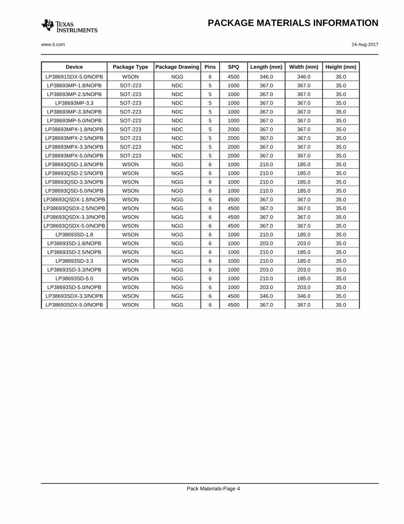
Device Package Type Package Drawing Pins SPQ Length (mm) Width (mm) Height (mm)
LP38691SDX-5.0/NOPB WSON NGG 6 4500 346.0 346.0 35.0
LP38693MP-1.8/NOPB SOT-223 NDC 5 1000 367.0 367.0 35.0
LP38693MP-2.5/NOPB SOT-223 NDC 5 1000 367.0 367.0 35.0
LP38693MP-3.3 SOT-223 NDC 5 1000 367.0 367.0 35.0
LP38693MP-3.3/NOPB SOT-223 NDC 5 1000 367.0 367.0 35.0
LP38693MP-5.0/NOPB SOT-223 NDC 5 1000 367.0 367.0 35.0
LP38693MPX-1.8/NOPB SOT-223 NDC 5 2000 367.0 367.0 35.0
LP38693MPX-2.5/NOPB SOT-223 NDC 5 2000 367.0 367.0 35.0
LP38693MPX-3.3/NOPB SOT-223 NDC 5 2000 367.0 367.0 35.0
LP38693MPX-5.0/NOPB SOT-223 NDC 5 2000 367.0 367.0 35.0
LP38693QSD-1.8/NOPB WSON NGG 6 1000 210.0 185.0 35.0
LP38693QSD-2.5/NOPB WSON NGG 6 1000 210.0 185.0 35.0
LP38693QSD-3.3/NOPB WSON NGG 6 1000 210.0 185.0 35.0
LP38693QSD-5.0/NOPB WSON NGG 6 1000 210.0 185.0 35.0
LP38693QSDX-1.8/NOPB WSON NGG 6 4500 367.0 367.0 35.0
LP38693QSDX-2.5/NOPB WSON NGG 6 4500 367.0 367.0 35.0
LP38693QSDX-3.3/NOPB WSON NGG 6 4500 367.0 367.0 35.0
LP38693QSDX-5.0/NOPB WSON NGG 6 4500 367.0 367.0 35.0
LP38693SD-1.8 WSON NGG 6 1000 210.0 185.0 35.0
LP38693SD-1.8/NOPB WSON NGG 6 1000 203.0 203.0 35.0
LP38693SD-2.5/NOPB WSON NGG 6 1000 210.0 185.0 35.0
LP38693SD-3.3 WSON NGG 6 1000 210.0 185.0 35.0
LP38693SD-3.3/NOPB WSON NGG 6 1000 203.0 203.0 35.0
LP38693SD-5.0 WSON NGG 6 1000 210.0 185.0 35.0
LP38693SD-5.0/NOPB WSON NGG 6 1000 203.0 203.0 35.0
LP38693SDX-3.3/NOPB WSON NGG 6 4500 346.0 346.0 35.0
LP38693SDX-5.0/NOPB WSON NGG 6 4500 367.0 367.0 35.0
PACKAGE MATERIALS INFORMATION
www.ti.com 24-Aug-2017
Pack Materials-Page 4
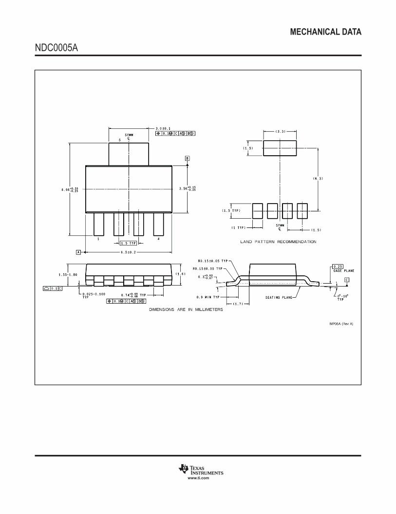
MECHANICAL DATA
NDC0005A
www.ti.com

www.ti.com
PACKAGE OUTLINE
C
10.429.40
6.736.35
6.225.97
1.270.88
5.464.96
2.285
4.57
1.020.64
3X 0.880.64
2.55 MAX
0.880.46
88
1.140.89
0.600.46
0.17
0.51 MIN
4.32 MIN
(2.345)
(2.5)
TO-252 - 2.55 mm max heightNDP0003BTRANSISTOR OUTLINE
4219870/A 03/2018
NOTES: 1. All linear dimensions are in millimeters. Any dimensions in parenthesis are for reference only. Dimensioning and tolerancing per ASME Y14.5M. 2. This drawing is subject to change without notice.3. Reference JEDEC registration TO-252.
0.25 C A B
TOP & BOTTOM
PKG
1
2
3
OPTIONAL
SEATING PLANE
4
3
2
1
SCALE 1.500
AB

www.ti.com
EXAMPLE BOARD LAYOUT
0.07 MAXALL AROUND
0.07 MINALL AROUND
(4.57)
2X (1.3)2X (2.15)
(5.7)
(5.5)
(2.285)(4.38)(R0.05) TYP
TO-252 - 2.55 mm max heightNDP0003BTRANSISTOR OUTLINE
4219870/A 03/2018
NOTES: (continued) 4. This package is designed to be soldered to a thermal pad on the board. For more information, see Texas Instruments literature numbers SLMA002(www.ti.com/lit/slm002) and SLMA004 (www.ti.com/lit/slma004).5. Vias are optional depending on application, refer to device data sheet. It is recommended that vias under paste be filled, plugged or tented.
LAND PATTERN EXAMPLEEXPOSED METAL SHOWN
SCALE: 8X
SYMM
PKG
1
3
4
SEE SOLDER MASKDETAIL
EXPOSEDMETAL
METAL EDGE
SOLDER MASKOPENING
NON SOLDER MASKDEFINED
(PREFERRED)SOLDER MASK DETAIL
EXPOSEDMETAL
METAL UNDERSOLDER MASK
SOLDER MASKOPENING
SOLDER MASK DEFINED

www.ti.com
EXAMPLE STENCIL DESIGN
2X (2.15)2X (1.3)
(4.57)
(4.38)
(1.32) TYP
(1.35) TYP
(0.26)(R0.05) TYP
16X (1.12)
16X (1.15)
TO-252 - 2.55 mm max heightNDP0003BTRANSISTOR OUTLINE
4219870/A 03/2018
NOTES: (continued) 6. Laser cutting apertures with trapezoidal walls and rounded corners may offer better paste release. IPC-7525 may have alternate design recommendations.7. Board assembly site may have different recommendations for stencil design.
PKG
SOLDER PASTE EXAMPLEBASED ON 0.125 MM THICK STENCIL
SCALE: 8X
MECHANICAL DATA
NGG0006A
www.ti.com
SDE06A (Rev A)

IMPORTANT NOTICE
Texas Instruments Incorporated (TI) reserves the right to make corrections, enhancements, improvements and other changes to itssemiconductor products and services per JESD46, latest issue, and to discontinue any product or service per JESD48, latest issue. Buyersshould obtain the latest relevant information before placing orders and should verify that such information is current and complete.TI’s published terms of sale for semiconductor products (http://www.ti.com/sc/docs/stdterms.htm) apply to the sale of packaged integratedcircuit products that TI has qualified and released to market. Additional terms may apply to the use or sale of other types of TI products andservices.Reproduction of significant portions of TI information in TI data sheets is permissible only if reproduction is without alteration and isaccompanied by all associated warranties, conditions, limitations, and notices. TI is not responsible or liable for such reproduceddocumentation. Information of third parties may be subject to additional restrictions. Resale of TI products or services with statementsdifferent from or beyond the parameters stated by TI for that product or service voids all express and any implied warranties for theassociated TI product or service and is an unfair and deceptive business practice. TI is not responsible or liable for any such statements.Buyers and others who are developing systems that incorporate TI products (collectively, “Designers”) understand and agree that Designersremain responsible for using their independent analysis, evaluation and judgment in designing their applications and that Designers havefull and exclusive responsibility to assure the safety of Designers' applications and compliance of their applications (and of all TI productsused in or for Designers’ applications) with all applicable regulations, laws and other applicable requirements. Designer represents that, withrespect to their applications, Designer has all the necessary expertise to create and implement safeguards that (1) anticipate dangerousconsequences of failures, (2) monitor failures and their consequences, and (3) lessen the likelihood of failures that might cause harm andtake appropriate actions. Designer agrees that prior to using or distributing any applications that include TI products, Designer willthoroughly test such applications and the functionality of such TI products as used in such applications.TI’s provision of technical, application or other design advice, quality characterization, reliability data or other services or information,including, but not limited to, reference designs and materials relating to evaluation modules, (collectively, “TI Resources”) are intended toassist designers who are developing applications that incorporate TI products; by downloading, accessing or using TI Resources in anyway, Designer (individually or, if Designer is acting on behalf of a company, Designer’s company) agrees to use any particular TI Resourcesolely for this purpose and subject to the terms of this Notice.TI’s provision of TI Resources does not expand or otherwise alter TI’s applicable published warranties or warranty disclaimers for TIproducts, and no additional obligations or liabilities arise from TI providing such TI Resources. TI reserves the right to make corrections,enhancements, improvements and other changes to its TI Resources. TI has not conducted any testing other than that specificallydescribed in the published documentation for a particular TI Resource.Designer is authorized to use, copy and modify any individual TI Resource only in connection with the development of applications thatinclude the TI product(s) identified in such TI Resource. NO OTHER LICENSE, EXPRESS OR IMPLIED, BY ESTOPPEL OR OTHERWISETO ANY OTHER TI INTELLECTUAL PROPERTY RIGHT, AND NO LICENSE TO ANY TECHNOLOGY OR INTELLECTUAL PROPERTYRIGHT OF TI OR ANY THIRD PARTY IS GRANTED HEREIN, including but not limited to any patent right, copyright, mask work right, orother intellectual property right relating to any combination, machine, or process in which TI products or services are used. Informationregarding or referencing third-party products or services does not constitute a license to use such products or services, or a warranty orendorsement thereof. Use of TI Resources may require a license from a third party under the patents or other intellectual property of thethird party, or a license from TI under the patents or other intellectual property of TI.TI RESOURCES ARE PROVIDED “AS IS” AND WITH ALL FAULTS. TI DISCLAIMS ALL OTHER WARRANTIES ORREPRESENTATIONS, EXPRESS OR IMPLIED, REGARDING RESOURCES OR USE THEREOF, INCLUDING BUT NOT LIMITED TOACCURACY OR COMPLETENESS, TITLE, ANY EPIDEMIC FAILURE WARRANTY AND ANY IMPLIED WARRANTIES OFMERCHANTABILITY, FITNESS FOR A PARTICULAR PURPOSE, AND NON-INFRINGEMENT OF ANY THIRD PARTY INTELLECTUALPROPERTY RIGHTS. TI SHALL NOT BE LIABLE FOR AND SHALL NOT DEFEND OR INDEMNIFY DESIGNER AGAINST ANY CLAIM,INCLUDING BUT NOT LIMITED TO ANY INFRINGEMENT CLAIM THAT RELATES TO OR IS BASED ON ANY COMBINATION OFPRODUCTS EVEN IF DESCRIBED IN TI RESOURCES OR OTHERWISE. IN NO EVENT SHALL TI BE LIABLE FOR ANY ACTUAL,DIRECT, SPECIAL, COLLATERAL, INDIRECT, PUNITIVE, INCIDENTAL, CONSEQUENTIAL OR EXEMPLARY DAMAGES INCONNECTION WITH OR ARISING OUT OF TI RESOURCES OR USE THEREOF, AND REGARDLESS OF WHETHER TI HAS BEENADVISED OF THE POSSIBILITY OF SUCH DAMAGES.Unless TI has explicitly designated an individual product as meeting the requirements of a particular industry standard (e.g., ISO/TS 16949and ISO 26262), TI is not responsible for any failure to meet such industry standard requirements.Where TI specifically promotes products as facilitating functional safety or as compliant with industry functional safety standards, suchproducts are intended to help enable customers to design and create their own applications that meet applicable functional safety standardsand requirements. Using products in an application does not by itself establish any safety features in the application. Designers mustensure compliance with safety-related requirements and standards applicable to their applications. Designer may not use any TI products inlife-critical medical equipment unless authorized officers of the parties have executed a special contract specifically governing such use.Life-critical medical equipment is medical equipment where failure of such equipment would cause serious bodily injury or death (e.g., lifesupport, pacemakers, defibrillators, heart pumps, neurostimulators, and implantables). Such equipment includes, without limitation, allmedical devices identified by the U.S. Food and Drug Administration as Class III devices and equivalent classifications outside the U.S.TI may expressly designate certain products as completing a particular qualification (e.g., Q100, Military Grade, or Enhanced Product).Designers agree that it has the necessary expertise to select the product with the appropriate qualification designation for their applicationsand that proper product selection is at Designers’ own risk. Designers are solely responsible for compliance with all legal and regulatoryrequirements in connection with such selection.Designer will fully indemnify TI and its representatives against any damages, costs, losses, and/or liabilities arising out of Designer’s non-compliance with the terms and provisions of this Notice.
Mailing Address: Texas Instruments, Post Office Box 655303, Dallas, Texas 75265Copyright © 2018, Texas Instruments Incorporated