lm096-128064 oled module specification -...
TRANSCRIPT

(Preliminary)
PartPartPartPartName:Name:Name:Name: OLED Display Module
PartPartPartPart ID:ID:ID:ID: LM096-128064
LI YUAN ELECTRONICS CO., LTD.Notes:Notes:Notes:Notes:
1. Please contact Li Yuan Electronics Co., Ltd. before assigning your productbased on this module specification.
2. The information contained herein is presented merely to indicate thecharacteristics and performance of our products. No responsibility is assumedby For any intellectual property claims orother problems that may result from application baesd on the moduledescribed herein.
PREPREPREPREPPPPAREDAREDAREDARED BYBYBYBY CHECKEDCHECKEDCHECKEDCHECKED BYBYBYBY APPROVEDAPPROVEDAPPROVEDAPPROVED BYBYBYBY
Li Yuan Electronics Co., Ltd..
E-mail: [email protected]
LI YUAN ELECTRONICS CO., LTD.
LM096-128064
Product Specification

RevisedRevisedRevisedRevised HistoryHistoryHistoryHistory
Part Number REV Revision Content Revised
LM096-128064 A First 20110918
E-mail: [email protected]
LI YUAN ELECTRONICS CO., LTD.
1 LM096-128064

Notce:Notce:Notce:Notce:
No part of this material may be reproduces or duplicated in any form or by
any means without the written permission of Li Yuan Electronics Co.,
Ltd. . Li Yuan Electronics Co., Ltd. reserves the right to make changes
to this material without notice. does not
assume any liability of any kind arising out of any inaccuracies contained
in this material or due to its application or use in any product or circuit ane,
further, there is no representation that this material is applicable to
products requiring high level reliability, such as, medical products.
Moreover, no license to any intellectual property rights is granted by
accordance with this material will be free from any patent or copyright
infringement of a to strategic products under the control of Foreign
Exchange and Foreign Trade Law of China and may require an export
license from the Ministry of International Trade and Industry or other
approval from another government agency.
Li Yuan Electronics Co., Ltd.
E-mail: [email protected]
LI YUAN ELECTRONICS CO., LTD.
2 LM096-128064

E-mail: [email protected]
LI YUAN ELECTRONICS CO., LTD.
ContentsContentsContentsContentsRevision History..................................................................................................... Notice 2Contents
1. Basic Specifications 5~8
1.1 Display Specifications 5
1.2 Mechanical Specifications 51.3 Active Area &Pixel 51.4 Mechanical Drawing 6
1.5 Pin Definition
9
1.6 Elements Block Diagram 8
2. Absolute Maximum Ratings 9
3. Electrical Characteristics
3.1 DC Characteristics
3.2 Optics & Electrical Characteristics
3.3 AC Characteristics
3.3.1 68XX-Series MPU Parallel Interface Timing
3.3.2 80XX-Series MPU Parallel Interface Timing
3.3.3 Serial Interface Timing Characteristics (4-SPI)
4. Functional Specification
......................................................................................................................
...............................................................................................................
........................................................................................
................................................................................
.........................................................................
..................................................................................
.................................................................................
.............................................................................................
...........................................................................
............................................................................
9~13............................................................................
......................................................................................
7
10...............................................................
10.....................................................................................
10......................................
......................................11...................................... 12
15~23..............................................................................
3~4
1
4.1 MCU parallel 6800-series interface
4.2 MCU parallel 8080-series interface
4.3 MCU Serial Interface (4-SPI)
4.5 MCU I2C Interface
4.5.1 I2C-bus Write data
15
16
............................................................
............................................................
17.......................................................................
.................................................................................... 19
19............................................................................
4.5.2 Write mode for I2C
4.6 Comman Decoder
4.7 FR synchronization
20.............................................................................
22.......................................................................................
22.....................................................................................
4.8 Rese Circuit 22.................................................................................................
3
3.3.5 I2C Interface Timing Characteristics ...................................................14
3.3.4 Serial Interface Timing Characteristics (3-SPI)...................................... 13
4.4 MCU Serial Interface (3-SPI) 18.......................................................................

5. Reliability 235.1 Contents of Reliability Tests
5.2 Life time
5.3 Failure Check Standard
6. Outgoing Quality Control Specifications
6.1 Environment Required
6.2 Sampling Plan
6.3 Criteria & Acceptable Quality Level
6.3.1 Cosmetic Check in Non-Active Area
6.3.2 Cosmetic Check in Active Area
6.3.3 Pattern Check in Active Area
7. Precaution When Using These OLED Display Module
E-mail: [email protected]
7.1 Handling Precautions
7.2 Srorage Precautions
7.3 Designing Precautions
7.4 Precaution when disposing of the OLED display modules
7.5 Other Precautions
8. Appendixes
8.1 Display-module Software Initial Setting
............................................................................................................................................................................. 23
................................................................................................... 23............................................................................ 23
24~26....................................................
.............................................................................. 24
........................................................................................... 24
...........................................................24
............................................. 24
.................................................... 25
........................................................ 26
27~29.......................................
................................................................................. 27
...................................................................................28
................................................................................28
........................... 28
29......................................................................................
......................................................................................................
30.....................................................
LI YUAN ELECTRONICS CO., LTD.
4
30
LM096-128064

1111 BasicBasicBasicBasic SpecificationsSpecificationsSpecificationsSpecifications
1.1 Display Specifications
1.2 Mechanical Specifications
1.3 Active Area & Pixel Construction
Item SpecsDisplay Mode Passive Matrix OLED&Blue,White,Yellow-BlueInterface 8-Bit 68XX/80XX Parallel、3/4-Wire SPI、I2CDrive Duty 1/64Driver IC SSD1306Shell 0.5TOther
Item Specs Unit RemarkOutline Drawing 34.7(W)x29.8(H)x4.95Max(T) mmView Area 26.7(W)x19.26(H) mmActive Area 21.744(W)x10.864(H) mmLattice 128dots x 64dots --Pixel Pitch 0.17(W)x0.17(H) mmPixel Size 0.154(W)x0.154(H) mm
E-mail: [email protected]
LI YUAN ELECTRONICS CO., LTD.
5
"A"
Segment 0( Column 128 )
Common 0( Row 64 )
Common 31( Row 2 )
Segment 127( Column 1 )
Common 32( Row 63 )
Common 63( Row 1 )
Detail "A"Scale (10:1)
P0.17x128-0.016=21.744
P0.1
7x64
-0.0
16=1
0.86
4
0.1540.17
0.15
40.
17
LM096-128064

1.4 Mechanical Drawing
mm
UN
IT
MO
DU
LEN
O.
CH
ECK
ED
SC
ALE
A4
SIZ
E
FIT
DES
IGN
ED
VE
RIF
IED
AP
PR
OVE
DFI
LE N
AME
LM09
6-1
2806
4
Cou
nt D
raw
ing
Gla
ss N
o.
Cou
nV
ER.
#1
t dra
win
g's
mod
ified
reco
rd w
ith c
usto
mer
THE
FIR
ST IS
SUE
DES
CR
IPTI
ON
2011
- 11
-18
DA
TE
E-mail: [email protected] LM096-128064
LI YUAN ELECTRONICS CO., LTD.
6
Pin Assig
nmen
t 1
VCC
2 GN
D 3
CS#
4 RE
S#
5 D/C#
6
R/W#
7 E/RD
# 8
D0
9 D1
10
D2
11
D3
12
D4
13
D5
14
D6
15
D7
16
NC
Blu
e,W
hit
e,Y
ell
ow
-Blu
e
SS
D13
06
Dav
ide
2011
-11-
18

1.5 Pin Definition
Pin No. Symbol I/O Function
1
GND P2
VCC 3-5.5V This is a voltage supply pin. It connected to externalsource.
3 CS# I
4 RES# I
5 D/C# I
6 R/W# I
7 E/RD# I
E-mail: [email protected]
LI YUAN ELECTRONICS CO., LTD.
7
CChhiipp SSeelleecctt This pin is the chip select input. The chip is enabled foMCU communication only when CS# is pulled low. oowweerr RReesseett ffoorr CCoonnttrroolllleerr aanndd DDrriivveerr This pin is reset signal input. When the pin is low,initialization of the chip is executed.
PP
aattaa//CCoommmmaanndd CCoonnttrrooll This pin is Data/Command control pin. When the pin ispulled high, the input at D7~D0 is treated as display data.When the pin is pulled low, the input at D7~D0 will betransferred to the command register. For detailrelationship to MCU interface signals, please refer to theTiming Characteristics Diagrams. When the pin is pulled high and serial interface mode isselected, the data at SDIN is treated as data. When it ispulled low, the data at SDIN will be transferred to thecommand register. In I2C mode, this pin acts as SA0 forslave address selection.
DD
RReeaadd//WWrriittee SSeelleecctt oorr WWrriittee This pi n is MCU interface input. When interfacing to 68XX-series microprocessor, this pin will be used asRead/Write (R/W#) selection input. Pull this pin to“High” for read mode and pull it to “Low” for writemode. When 80XX interface mode is selected, this pin will bethe Write (WR#) input. Data write operation is initiatewhen this pin is pulled low and the CS# is pulled low.
RReeaadd//WWrriittee EEnnaabbllee oorr RReeaadd This pin is MCU interface input. When interfacing to 68XX-series microprocessor, this pin will be used as theEnable (E) signal. Read/write operation is initiated whethis pin is pulled high and the CS# is pulled low. When connecting to an 80XX-microprocessor, this pinreceives the Read (RD#) signal. Data read operation isinitiated when this pin is pulled low and CS# is pulledlow.
GGrroouunndd ooff AAnnaalloogg CCiirrccuuiitt This is an analog ground pin. It should be connected toVSS externally.
Power Supply for Display Module Circuit Power Supply for Display Module Circuit
8-15 D0-D7 I/O
HHoosstt DDaattaa IInnppuutt//OOuuttppuutt BBuuss These pins are 8-bit bi-directional data bus to beconnected to the microprocessor’s data bus. When serialmode is selected, D1 will be the serial data input SDINand D0 will be the serial clock input SCLK. When I2Cmode is selected, D2 & D1 should be tired together anserve as SDAout & SDAin in application and D0 is theserial clock input SCL.
LM096-128064

1.6 Elements Block Diagram
MCU Interface Selection: BS1 and BS2Pins Connected to MCU interface:D7~D0,R/W#, E/RD#, D/C#, CS#, RES#.
16 NC - Float or connect to VSS.
E-mail: [email protected]
LI YUAN ELECTRONICS CO., LTD.
8
RReesseerrvveedd PPiinn
CommonDriver
Oscillator
Graphic Display DataRAM (GDDRAM)
MCUInterface Command
Decoder
RES
#C
S#D
/C#
E (R
D#)
R/W
#(W
R#)
BS2 BS1
BS0 D7
D6
D5
D4
D3
D2
D1
D0
Charge pump Regulator
Current ControlVoltage Control
VD
D
SEG
0SE
G1
| | CO
M1
CO
M3
| | CO
M61
CO
M63
CO
M6 2
CO
M60
| | CO
M2
CO
M0
Display ControllerV
SSV
LSS
CommonDriver
SegmentDriver
BS0,
MCU Bus Interface Pin Selection
Pin Name I2C Interface
6800-parallel interface (8 bit)
8080-parallel interface(8 bit)
4-wire Serial interface
3-wire Serial interface
BS0 0 0 0 0 1 BS1 1 0 1 0 0 BS2 0 1 1 0 0
Note (1) 0 is connected to VSS (2) 1 is connected to VDD
interface(8 bit)
Default interface is 8080-parallel.(3) Please tell us the specific requirement of your company,we will provide appropriate interface to you.(4)
LM096-128064

2.2.2.2.AbsoluteAbsoluteAbsoluteAbsoluteMaximumMaximumMaximumMaximumRatingsRatingsRatingsRatings
Note 1: All the above voltage are on the basis of “GND=0V”.Note 2: When this module is used beyond the above absolute maximum
Ratings, permanent breakage of the module may occur. Also, for normaloperations, it is desirable to use this module under the conditions accordingto Section 3. “Electrical Characteristics”. If this module is used beyondthese conditions, malfunctioning of the module can occur and the reliabilityof the module may deteriorate.
3.Electrical3.Electrical3.Electrical3.ElectricalCharacteristicsCharacteristicsCharacteristicsCharacteristics
3.1 DC Charateristics
Note1: VCC=3.7V, 50% Display Area Turn on;
Parameter Symbol Min Max Unit Notes
Power Supply Voltage VCC 6 V 1,2
Power Supply Current Icc - 18 mA 1,2
Operating Temperature Top -30 70 ℃ ----
Storage Temperature Tstg -40 80 ℃ ----
Characteristics Symbol Conditions Min Typ Max Unit
Supply Voltage VCC 3.0 - 5.5 V
High Level Input VIHIout=100uA3.3MHz 1.32 - 3.6 V
Low Level Input VILIout=100uA3.3MHz 0 - 0.7 V
Supply Current IccNote1 -
12.3
mA
E-mail: [email protected]
LI YUAN ELECTRONICS CO., LTD.
9
2
Ta=25℃
Note2
9.17.3
15.4 mA
Sleep Mode Current Icc, Sleep
-
- 1 5 uA
Note2: VCC=3.7V, 100% Display Area Turn on.
LM096-128064

3.2 Optics & Electrical Characteristics
* Optical measurement taken at VDD =2.8V.VCC=9.0V,and software configurationfollows “Software Initial Setting”.
3.3 AC Characteristics
3.3.1 68XX-Series MPU Parallel Interface Timing Characteristics:
Characteristics Symbol Conditions Min Typ Max Unit
Brightness LbrWith Polarizer
(Note 3)80 100 - Cd/m2
C.I.E.(White)(X)(Y)
With Polarizer0.280.29
0.320.33
0.360.37
Dark Room Contrast CR - >2000:1 -View Angle >160 - - degree
E-mail: [email protected]
LI YUAN ELECTRONICS CO., LTD.
10
Symbol Description Min Max Unittcycle Clock Cycle Time 300 - ns tAS Address Setup Time 0 - ns tAH Address Hold Time 0 - ns
tDSW Write Data Setup Time 40 - ns tDHW Write Data Hold Time 7 - ns tDHR Read Data Hold Time 20 - ns tOH Output Disable Time - 70 ns tACC Access Time - 140 ns
Chip Select Low Pulse Width (Read) 120 PWCSL
Chip Select Low Pulse width (Write) 60 - ns
Chip Select High Pulse Width (Read) 60 PWCSH
Chip Select High Pulse Width (Write) 60 - ns
tR Rise Time - 40 ns tF Fall - 40 ns
* (V - VSS = 1.65V to 3.3V, Ta = 25°C)DD
LM096-128064
C.I.E.(Blue)(X)(Y)
With Polarizer0.120.22
0.160.26
0.200.30
C.I.E.(Yellow)(X)(Y)
With Polarizer0.440.46
0.480.50
0.520.54

3.3.2 80XX-Series MPU Parallel Interface Timing Charavteristics:
E-mail: [email protected]
LI YUAN ELECTRONICS CO., LTD.
11
Symbol Description Min Max Unittcycle Clock Cycle Time 300 - ns tAS Address Setup Time 10 - ns tAH Address Hold Time 0 - ns
tDSW Write Data Setup Time 40 - ns tDHW Write Data Hold Time 7 - ns tDHR Read Data Hold Time 20 - ns tOH Output Disable Time - 70 ns tACC Access Time - 140 ns tPWLR Read Low Time 120 - ns tPWLW Write Low Time 60 - ns tPWHR Read High Time 60 - ns tPWHW Write High Time 60 - ns
tCS Chip Select Setup Time 0 - ns tCSH Chip Select Hold Time to Read Signal 0 - ns tCSF Chip Select Hold Time 20 - ns t Rise Time - 40 ns tF Fall Time - 40 ns
* (VDD - VSS = 1.65V to 3.3V, Ta = 25°C)
LM096-128064

3.3.3 Serial Interface Timing Characteristics: (4-wire SPI)
E-mail: [email protected]
LI YUAN ELECTRONICS CO., LTD.
12
( Read Timing )
( Write Timing )
Symbol Description Min Max Unittcycle Clock Cycle Time 100 - ns tAS Address Setup Time 15 - ns tAH Address Hold Time 15 - ns tCSS Chip Select Setup Time 20 - ns tCSH Chip Select Hold Time 10 - ns tDSW Write Data Setup Time 15 - ns tDHW Write Data Hold Time 15 - ns tCLKL Clock Low Time 20 - ns tCLKH Clock High Time 20 - ns
tR Rise Time - 40 ns tF Fall Time - 40 ns
* (VDD - VSS = 1.65V to 3.3V, Ta = 25°C)
LM096-128064

E-mail: [email protected]
LI YUAN ELECTRONICS CO., LTD.
13
3.3.4 Serial Interface Timing Characteristics: (3-wire SPI)
Symbol Description Min Max Unittcycle Clock Cycle Time 100 - ns tCSS Chip Select Setup Time 20 - ns tCSH Chip Select Hold Time 10 - ns tDSW Write Data Setup Time 15 - ns tDHW Write Data Hold Time 15 - ns tCLKL Clock Low Time 20 - ns tCLKH Clock High Time 20 - ns
tR Rise Time - 40 ns tF Fall Time - 40 ns
* (VDD - VSS = 1.65V to 3.3V, Ta = 25°C)
LM096-128064

3.3.5 I2C Interface Timing Characteristics:
E-mail: [email protected]
LI YUAN ELECTRONICS CO., LTD.
14
Symbol Description Min Max Unittcycle Clock Cycle Time 2.5 - us
tHSTART Start Condition Hold Time 0.6 - us Data Hold Time (for “SDAOUT” Pin) 0
tHD Data Hold Time (for “SDAIN” Pin) 300
- ns
tSD Data Setup Time 100 - ns
tSSTART Start Condition Setup Time (Only relevant for a repeated Start condition)
0.6 - us
tSSTOP Stop Condition Setup Time 0.6 - us tR Rise Time for Data and Clock Pin 300 ns tF Fall Time for Data and Clock Pin 300 ns
tIDLE Idle Time before a New Transmission can Start 1.3 - us
* (VDD - VSS = 1.65V to 3.3V, Ta = 25°C)
LM096-128064

4444 FunctionalFunctionalFunctionalFunctional SpecificatonSpecificatonSpecificatonSpecificaton
MCUMCUMCUMCU InterfaceInterfaceInterfaceInterface selection:selection:selection:selection:
4.1 MCU parallel 6800-series interface
The parallel interface consists of 8 bi-directional data pins (DB[7:0]), R/W#, D/C#, Eand CS#. A LOW in R/W# indicates WRITE operation and HIGH in R/W# indicatesREAD operation. A LOW in D/C# indicates COMMAND read/write and HIGH inD/C# indicates DATA read/write. The E input serves as data latch signal while CS#is LOW. Data is latched at the falling edge of E signal.
Note (1) ↓ stands for falling edge of signalH stands for HIGH in signalL stands for LOW in signal
In order to match the operating frequency of display RAM with that of themicroprocessor, some pipeline processing is internally performed which requires theinsertion of a dummy read before the first actual display data read. This is shown asfollows.
Data read back procedure - insertion of dummy read
E-mail: [email protected]
LI YUAN ELECTRONICS CO., LTD.
15
Data/Command Interface Control Signal Pin Name Bus Interface D7 D6 D5 D4 D3 D2 D1 D0 E R/W# CS# D/C# RES# 8-bit 8080 D[7:0] RD# WR# CS# D/C# RES# 8-bit 6800 D[7:0] E R/W# CS# D/C# RES# 3-wire SPI Tie LOW NC SDIN SCLK Tie LOW CS# Tie LOW RES# 4-wire SPI Tie LOW NC SDIN SCLK Tie LOW CS# D/C# RES# I2C Tie LOW SDAOUT SDAIN SCL Tie LOW SA0 RES#
Control pins of 6800 interface
Function E R/W# CS# D/C#
Write command ↓ L L L
Read status ↓ H L L
Write data ↓ L L H
Read data ↓ H L H
LM096-128064

4.2 MCU parallel 8080-series interface
The parallel interface consists of 8 bi-directional data pins (DB[7:0]), RD#, WR#,D/C# and CS#. A LOW in D/C# indicates COMMAND read/write and HIGH in D/C#indicates DATA read/write. A rising edge of RD# input serves as a data READlatch signal while CS# is kept LOW. A rising edge of WR# input serves as adata/command WRITE latch signal while CS# is kept LOW.
E-mail: [email protected]
LI YUAN ELECTRONICS CO., LTD.
16
Example of Write procedure in 8080 parallel interface mode
CS#
WR#
D[7:0]
D/C#
RD#high
low
Example of Read procedure in 8080 parallel interface mode
CS#
WR#
D[7:0]
D/C#
RD#
high
low
Control pins of 8080 interface
Function RD# WR# CS# D/C# Write command H ↑ L L Read status ↑ H L L Write data H ↑ L H Read data ↑ H L H
Note (1) ↑ stands for rising edge of signal (2) H stands for HIGH in signal (3) L stands for LOW in signal
In order to match the operating frequency of display RAM with that of themicroprocessor, some pipeline processing is internally performed which requires theinsertion of a dummy read before the first actual display data read. This is shown asfollows.
LM096-128064

4.3 MCU Serial Interface (4-wire SPI)
The 4-wire serial interface consists of serial clock: SCLK, serial data: SDIN, D/C#, CS#.In 4-wire SPI mode, D0 acts as SCLK ,D1 acts as SDIN .For the unused data pins, D2should be left open. The pins from D3 to D7, E and R/W#(WR#) can be connected to anexternal ground.
SDIN is shifted into an 8-bit shift register on every rising edge of SCLK in theorder of D7, D6, ... D0. D/C# is sampled on every eighth clock and the data byte inthe shift register is written to the Graphic Display Data RAM (GDDRAM) orcommand register in the same clock. Under serial mode, only write operations areallowed.
E-mail: [email protected]
LI YUAN ELECTRONICS CO., LTD.
17
Display data read back procedure - insertion of dummy read
N n n+1 n+2
WR#
RD#
Write columnaddress Read 1st dataDummy read Read 2nd data Read 3rd data
Control pins of 4-wire Serial interface
Function E(RD#) R/W#(WR#) CS# D/C# D0 Write command Tie LOW Tie LOW L L ↑ Write data Tie LOW Tie LOW L H ↑
Note (1) H stands for HIGH in signal (2) L stands for LOW in signal
Write procedure in 4-wire Serial interface mode
D7 D6 D5 D4 D3 D2 D1 D0
SCLK (D0)
SDIN(D1)
DB1 DB2 DBn
CS#
D/C#
SDIN/ SCLK
LM096-128064

E-mail: [email protected]
LI YUAN ELECTRONICS CO., LTD.
18
4.4 MCU Serial Interface (3-wire SPI)
The 3-wire serial interface consists of serial clock: SCLK, serial data: SDIN, and CS#.In 3-wire SPI mode, D0 acts as SCLK ,D1 acts as SDIN .For the unused data pins, D2should be left open. The pins from D3 to D7, E, R/W#(WR#) and D/C# can be connected to an externalground.
The operation is similar to 4-wire serial interface while D/C# pin is not used. There arealtogether 9-bits will be shifted into the shift register on every ninth clock in sequence:D/C# bit, D7 to D0 bit. The D/C# bit (first bit of the sequential data) will determine thefollowing data byte in the shift register is written to the display Data RAM (D/C# bit=1)or the command register (D/C# bit = 0). Under serial mode, only write operation are allowed.
Control pins of 3-wire Serial interface
Function E(RD#) R/W#(WR#) CS# D/C# D0Write command Tie LOW Tie LOW L Tie LOW ↑Write data Tie LOW Tie LOW L Tie LOW ↑
Note (1) L stands for LOW in signal
Write procedure in 3-wire Serial interface mode
D7 D6 D5 D4 D3 D2 D1 D0
SCLK (D0)
SDIN(D1)
DB1 DB2 DBn
CS#
D/C#
SDIN/ SCLK
LM096-128064

4.5 MCU I2C Interface
The I2C communication interface consists of slave address bit SA0, I2C-busdata signal SDA(SDAOUT/D2 for output and SDAIN/D1 for input) and I2C-bus clock signal SCL (D0). Both the data and clock signals must be connected topull-up resistors. /RES is used for the initialization of device.
a) Slave address bit (SA0)SSD1306 has to recognize the slave address before transmitting or receiving anyinformation by the I2C-bus. The device will respond to the slave addressfollowing by the slave address bit(“SA0” bit) and the read/write select bit(“R/W#” bit) with the following byte format,b7 b6 b5 b4 b3 b2 b1 b00 1 1 1 1 0 SA0 R/W
“SA0” bit provides an extension bit for the slave address. Either “0111100” or“0111101”, can be selected as the slave address of SSD1306. DC pin acts as SA0for slave address selection. “R/W” bit is used to determine the operation modeof the I2C-bus interface. R/W=1, it is in read mode. R/W=0, it is in write mode.
b) I2C-bus data signal (SDA) SDA acts as a communication channel between thetransmitter and the receiver. The data and the acknowledgement are sent throughthe SDA.It should be noticed that the ITO track resistance and the pulled-up resistance at“SDA” pin becomes a voltage potential divider. As a result, theacknowledgement would not be possible to attain a valid logic 0 level in “SDA”.“SDAIN” and “SDAOUT” are tied together and serve as SDA. The “SDAIN”pin must be connected to act as SDA. The “SDAOUT” pin may be disconnected.When “SDAOUT” pin is disconnected, the acknowledgement signal will beignored in the I2C-bus.
b) I2C-bus clock signal (SCL)The transmission of information in the I2C-bus is following a clock signal, SCL.Each transmission of data bit is taken place during a single clock period of SCL.
4.5.1 I2C-bus Write data
The I2C-bus interface gives access to write data and command into the device.Please refer to the following Figure for the write mode of I2C-bus inchronological order.
E-mail: [email protected]
LI YUAN ELECTRONICS CO., LTD.
19 LM096-128064
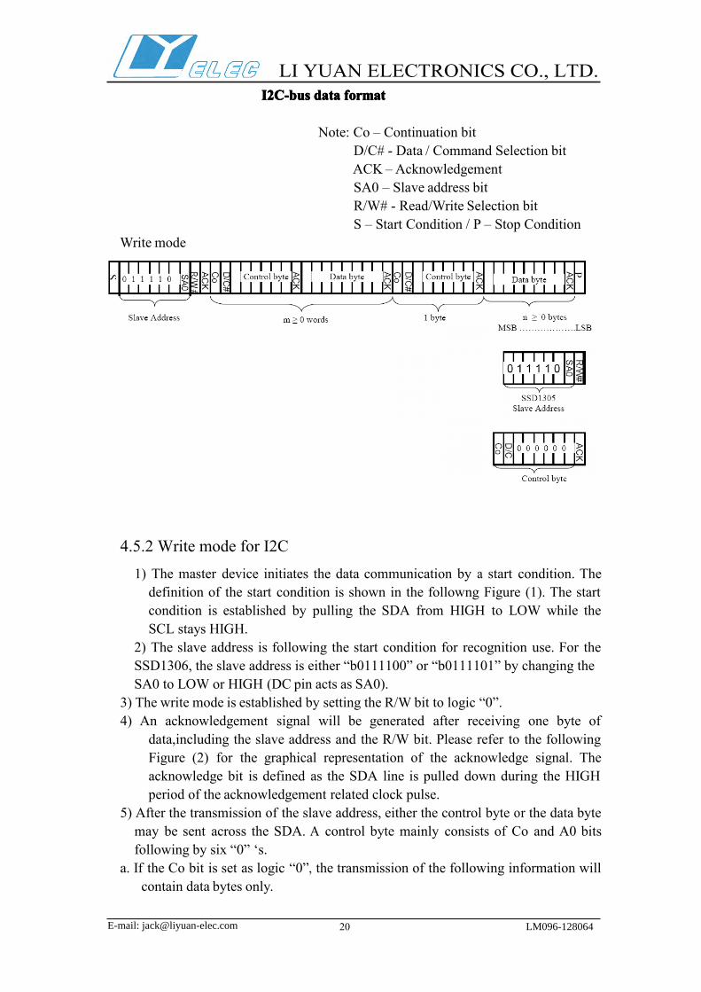
I2CI2CI2CI2C-bus-bus-bus-bus datadatadatadata formatformatformatformat
Note: Co – Continuation bitD/C# - Data / Command Selection bitACK – AcknowledgementSA0 – Slave address bitR/W# - Read/Write Selection bitS – Start Condition / P – Stop Condition
Write mode
4.5.2 Write mode for I2C
1) The master device initiates the data communication by a start condition. Thedefinition of the start condition is shown in the followng Figure (1). The startcondition is established by pulling the SDA from HIGH to LOW while theSCL stays HIGH.
2) The slave address is following the start condition for recognition use. For theSSD1306, the slave address is either “b0111100” or “b0111101” by changing theSA0 to LOW or HIGH (DC pin acts as SA0).
3) The write mode is established by setting the R/W bit to logic “0”.4) An acknowledgement signal will be generated after receiving one byte of
data,including the slave address and the R/W bit. Please refer to the followingFigure (2) for the graphical representation of the acknowledge signal. Theacknowledge bit is defined as the SDA line is pulled down during the HIGHperiod of the acknowledgement related clock pulse.
5) After the transmission of the slave address, either the control byte or the data bytemay be sent across the SDA. A control byte mainly consists of Co and A0 bitsfollowing by six “0” ‘s.
a. If the Co bit is set as logic “0”, the transmission of the following information willcontain data bytes only.
E-mail: [email protected]
LI YUAN ELECTRONICS CO., LTD.
20 LM096-128064

b. The A0 bit determines the next data byte is acted as a command or a data. If the A0bit is set to logic “0”, it defines the following data byte as a command. If the A0 bitis set to logic “1”, it defines the following data byte as a data which will be storedat the GDDRAM. The GDDRAM column address pointer will be increased byone automatically after each data write.
6) Acknowledge bit will be generated after receiving each control byte or data byte.7) The write mode will be finished when a stop condition is applied. The stop
condition is also defined in Figure (1). The stop condition is established bypulling the “SDA in” from LOW to HIGH while the “SCL” stays HIGH.
Figure (1): Definition of the Start and Stop Condition
Figure (2):Definition of the acknowledgement condition
Please be noted that the transmission of the data bit has some limitations.1. The data bit, which is transmitted during each SCL pulse, must keep at a stable state
within the “HIGH” period of the clock pulse. Please refer to the Figure (3) forgraphical representations.Except in start or stop conditions, the data line can beswitched only when the SCL is LOW.
2. Both the data line (SDA) and the clock line (SCL) should be pulled up by externalresistors.
E-mail: [email protected]
LI YUAN ELECTRONICS CO., LTD.
21 LM096-128064

Figure (3):Definition of the data transfer condition
4.6 Command Decoder
Refe to the Technical Manual for the SSD1306.
4.7 FR synchronization
Refer to the Technical Manual for the SSD1306.
4.8 Reset Circuit
When /RES input is low, the chip is initialized with the following status:1. Display is OFF.2. 128x64 MUX Display Mode.3. Normal segment and display data column address and row address mapping
(SEG0 mapped to address 00h and COM0 mapped to address 00h).4. Shift register data clear in serial interface.5. Display start line is set at display RAM address 0.6. Column address counter is set at 0.7. Normal scan direction of the COM outputs.8.Contrast control register is set at 7Fh.9. Normal display mode (Equivalent to A4h command).
E-mail: [email protected]
LI YUAN ELECTRONICS CO., LTD.
22 LM096-128064

5.5.5.5. ReliabilityReliabilityReliabilityReliability
5.1 Contents of Reliability Tests
* The samples used for the above tests do not include polarizer.* No moisture condensation is observed during tests.
5.2 Life time
End of lifetime is specified as 50% of initial brightness.
Note 6: The average operating lifetime at room temperature is estimated by theaccelerated operation at high temperature conditions.
5.3 Failure Check Standard
After the completion of the described reliability test, the samples were leftat room temperature for 2 hrs prior to conducting the failure test at 23+/-5℃;55+/-15%RH.
Item Conditions CriteriaHigh Temperature Operation 85℃ TBD
The operationalFunctions work
Low Temperature Operation -40℃ TBDHigh Temperature Storage 90℃ TBDLow Temperature Storage -45℃ TBDHigh Temperature/HumidityOperation
60℃ TBD
Thermal Shock -40℃�90℃ TBD
Parameter Min Max Unit Condition NotesOperating Life Time 50,000 - Hrs 80 cd/m2,50%checkerboard 6Storage Life Time 200,000 - Hrs Ta=25 ℃,50%RH -
E-mail: [email protected]
LI YUAN ELECTRONICS CO., LTD.
23 LM096-128064

6.6.6.6. OutgoingOutgoingOutgoingOutgoing QualityQualityQualityQuality ControlControlControlControl SpecificationsSpecificationsSpecificationsSpecifications
6.1 Environment RequiredCustomer’s test & measurement are required to be conducted under thefollowing conditions:Temperature: 23+/-5℃Humidity: 55+/-15%RHFluorescent Lamp: 30WDistance between the Panel & Lamp: >=50 cmDistance between the Panel & Eyes of the Inspector >=30 cmFinger glove (or finger cover) must be worn by the inspector.Inspection table or jig must be anti-electrostatic.
6.2 Sampling Plan
Level II, Normal Inspection, Single Sampling,MIL-STD-105E
6.3 Criteria & Acceptable Quality Level
6.3.1 Cosmetic Check (Display Off) in Non-Active Area
Partition AQL DefinitionMajor 0.65 DefectsinPatternCheck(DisplayOn)Minor 1.0 Defects in Cosmetic Check (Display Off)
E-mail: [email protected]
LI YUAN ELECTRONICS CO., LTD.
24 LM096-128064

6.3.2
E-mail: [email protected]
LI YUAN ELECTRONICS CO., LTD.
25
Cosmetic Check (Display Off) in Active Area
Check Item Classification Criteria Any Dirt & Scratch on
Polarizer’s Protective Film Acceptable Ignore for not Affect the Polarizer
Scratches, Fiber, Line-Shape Defect
(On Polarizer) Minor
W ≤ 0.1 Ignore W > 0.1, L ≤ 2 n ≤ 1 L > 2 n = 0
Dirt, Black Spot, Foreign Material,
(On Polarizer) Minor
Φ ≤ 0.1 Ignore 0.1 <Φ ≤ 0.25 n ≤ 1 0.25 <Φ n = 0
Dent, Bubbles, White spot (Any Transparent Spot on
Polarizer) Minor
Φ ≤ 0.5 Ignore if no Influence on Display
0.5 < Φ n = 0
Fingerprint, Flow Mark (On Polarizer) Minor Not Allowable
* Protective film should not be tear off when cosmetic check. ** Definition of W & L & Φ (Unit: mm): Φ = (a + b) / 2
W
L
b: Minor Axis
a: Major Axis
LM096-128064

6.3.3 Pattern Check (Display On) in Active Area
E-mail: [email protected]
LI YUAN ELECTRONICS CO., LTD.
26
Check Item Classification Criteria
No Display Major
Flicker Major Not Allowable
Missing Line Major
Pixel Short Major
Darker Pixel Major
Wrong Display Major
Un-uniform Major
LM096-128064

7.7.7.7. PrecautionsPrecautionsPrecautionsPrecautionsWhenWhenWhenWhen UsingUsingUsingUsing TheseTheseThese OLED DisplayDisplay ModulesModules
7.1 Handling Precautions1) Since the display panel is being made of glass, do not apply mechanical
impacts such us dropping from a high position.2) If the display panel is broken by some accident and the internal organic
substance leaks out, be careful not to inhale nor lick the organic substance.3) If pressure is applied to the display surface or its neighborhood of the OLED
display module, the cell structure may be damaged and be careful not to applypressure to these sections.
4) The polarizer covering the surface of the OLED display module is soft andeasily scratched. Please be careful when handling the OLED display module.
5) When the surface of the polarizer of the OLED display module has soil,cleanthe surface. It takes advantage of by using following adhesion tape.* Scotch Mending Tape No. 810 or an equivalentNever try to breathe upon the soiled surface nor wipe the surface using clothcontaining solvent such as ethyl alcohol, since the surface of the polarizer willbecome cloudy.Also, pay attention that the following liquid and solvent may spoil the polarizer* Water* Ketone* Aromatic Solvents
6) When installing the OLED display module, be careful not to apply twistingstress or deflection stress to the OLED display module. And, do not over bendthe film with electrode pattern layouts. These stresses will influence thedisplay performance. Also, secure sufficient rigidity for the outer cases.
7) Do not apply stress to the LSI chips and the surrounding molded sections.8) Do not disassemble nor modify the OLED display module.9) Do not apply input signals while the logic power is off.10) Pay sufficient attention to the working environments when handing OLED
display modules to prevent occurrence of element breakage accidents bystatic electricity.
* Be sure to make human body grounding when handling OLED displaymodules.
* Be sure to ground tools to use or assembly such as soldering irons.* To suppress generation of static electricity, avoid carrying out assembly
work under dry environments.* Protective film is being applied to the surface of the display panel of theOLED display module. Be careful since static electricity may be generatedwhen exfoliating the protective film.
11) Protection film is being applied to the surface of the display panel andremoves the protection film before assembling it. At this time, if the OLEDdisplay module has been stored for a long period of time, residue adhesivematerial of the protection film may remain on the surface of the display
E-mail: [email protected]
LI YUAN ELECTRONICS CO., LTD.
27 LM096-128064
OLEDOLEDOLEDOLEDOLED

panel after removed of the film. In such case, remove the residue materialby the method introduced in the above Section 5).
12) If electric current is applied when the OLED display module is beingdewed or when it is placed under high humidity environments, theelectrodes may be corroded and be careful to avoid the above.
7.2 Storage Precautions1) When storing OLED display modules, put them in static electricity
preventive bags avoiding exposure to direct sun light nor to lights offluorescent lamps.and, also, avoiding high temperature and high humidityenvironment or low temperature (less than 0°C) environments. (Werecommend you to store these modules in the packaged state when theywere shipped from Li Yuan Electronics Co.,Ltd.)At that time, be careful not to let water drops adhere to the packages or bagsnor let dewing occur with them.
2) If electric current is applied when water drops are adhering to the surface ofthe OLED display module, when the OLED display module is being dewedor when it is placed under high humidity environments, the electrodes maybe corroded and be careful about the above.
7.3 Designing Precautions1) The absolute maximum ratings are the ratings which cannot be exceeded
for OLED display module, and if these values are exceeded, panel damagemay be happen.
2) To prevent occurrence of malfunctioning by noise, pay attention to satisfythe VIL and VIH specifications and, at the same time, to make the signalline cable as short as possible.
3) We recommend you to install excess current preventive unit (fuses, etc.) tothe power circuit (VDD). (Recommend value: 0.5A)
4) Pay sufficient attention to avoid occurrence of mutual noise interferencewith the neighboring devices.
5) As for EMI, take necessary measures on the equipment side basically.6) When fastening the OLED display module, fasten the external plastic
housing section.7) If power supply to the OLED display module is forcibly shut down by such
errors as taking out the main battery while the OLED display panel is inoperation, we cannot guarantee the quality of this OLED display module.
8) The electric potential to be connected to the rear face of the IC chip shouldbe as follows: SSD1331* Connection (contact) to any other potential than the above may lead torupture of the IC.
7.4 Precautions when disposing of the OLED display modules1) Request the qualified companies to handle industrial wastes when disposingof the OLED display modules. Or, when burning them, be sure to observethe environmental and hygienic laws and regulations.
E-mail: [email protected]
LI YUAN ELECTRONICS CO., LTD.
28 LM096-128064

7.5 Other Precautions1) When an OLED display module is operated for a long of time with fixed
pattern may remain as an after image or slight contrast deviation may occur.Nonetheless, if the operation is interrupted and left unused for a while, normalstate can be restored. Also, there will be no problem in the reliability of themodule.
2) To protect OLED display modules from performance drops by staticelectricity rapture, etc., do not touch the following sections whenever possiblewhile handling the OLED display modules.
* Pins and electrodes*Patternlayoutssuchasthe FPC
3) With this OLED display module, the OLED driver is being exposed.Generally speaking, semiconductor elements change their characteristics whenlight is radiated according to the principle of the solar battery. Consequently,if this OLED driver is exposed to light, malfunctioning may occur.* Design the product and installation method so that the OLED driver may beshielded from light in actual usage.
* Design the product and installation method so that the OLED driver may beshielded from light during the inspection processes.
4) Although this OLED display module stores the operation state data by thecommands and the indication data, when excessive external noise, etc. entersinto the module, the internal status may be changed. It therefore is necessaryto take appropriate measures to suppress noise generation or to protect frominfluences of noise on the system design.
5) We recommend you to construct its software to make periodical refreshmentof the operation statuses (re-setting of the commands and re-transference ofthe display data) to cope with catastrophic noise.
E-mail: [email protected]
LI YUAN ELECTRONICS CO., LTD.
29 LM096-128064

E-mail: [email protected]
LI YUAN ELECTRONICS CO., LTD.
30
8888.... AppendixesAppendixesAppendixesAppendixes
8.1 Display-module Software Initial Setting
Write_ Command(0xAE); //display offWrite_ Command(0x20); //Set Memory Addressing Mode<00FF>Write_ Command(0x10); //Addressing ModeeWrite_ Command(0xb0); //Set Page Start Address for Page Addressing Mode,0-7Write_ Command(0xc8); //Set COM Output Scan DirectionWrite_ Command(0x00); //---set low column addressWrite_ Command(0x10); //---set high column addressWrite_ Command(0x40); //--set start line addressWrite_ Command(0x81); //--set contrast control registerWrite_ Command(0xaf);Write_ Command(0xa1); //--set segment re-map 0 to 127Write_ Command(0xa6); //--set normal displayWrite_ Command(0xa8); //--set multiplex ratio(1 to 64)Write_ Command(0x3F);Write_ Command(0xa4); //0xa4,Output follows RAM content;0xa5,Output ignores RAM contentWrite_ Command(0xd3); //-set display offsetWrite_ Command(0x00); //-not offsetWrite_ Command(0xd5); //--set display clock divide ratio/oscillator frequencyWrite_ Command(0xf0); //--set divide ratioWrite_ Command(0xd9); //--set pre-charge periodWrite_ Command(0x22);Write_ Command(0xda); //--set com pins hardware configurationWrite_ Command(0x12);Write_ Command(0xdb); //--set vcomhWrite_ Command(0x20); //0x20,0.77xVccWrite_ Command(0x8d); //--set DC-DC enableWrite_ Command(0x14);Write_ Command(0xaf); //--turn on oled panel
LM096-128064