life pure xl service manual - ftpeil.eil.com.brftpeil.eil.com.br/vip/blu/life pure xl/life pure xl...
TRANSCRIPT

1 / 33
LIFE PURE XL Service
Manual

2 / 33
CONTENT
1 OUTLINE ................................................................................................................................ 3
1.1 MOBILE PHONE INTRODUCTION ................................................................................. 3
1.2 MAINBOARD COMPONENTS DISTRIBUTION ........................................................................... 5
2 SIGNAL FLOW AND FAULT ANALYSIS ................................................................................. 7
2.1 RF PART ............................................................................................................................ 7
2.1.1 Block Diagram of the RF Section .............................................................................. 7
2.1.2 Signal Flow OF the RF Transmitting Part ................................................................. 9
2.1.2.1 Receiving and Transmit Path ............................................................................. 9
2.1.2.2 Maintenance Procedures of the Transmitting Part ........................................... 10
2.1.3 Signal Flow of the Receiving Part ............................................................................ 11
2.1.3.1 Maintenance Procedures of the Receiving Part ........................................... 11
2.2 BASEBAND PART .............................................................................................................. 12
2.2.1 Block Diagram of the Baseband Part ...................................................................... 12
2.2.2 Power Management Part ........................................................................................ 13
2.2.2.1 The Whole Power Supply System ................................................................... 14
2.2.3 Audio Part................................................................................................................ 18
2.2.3.1 Audio CODEC Circuit ....................................................................................... 18
2.2.3.2 MIC and RECEIVER LOOP ............................................................................. 20
2.2.3.3 HEADSET LOOP ............................................................................................. 21
2.2.3.4 Speaker part ..................................................................................................... 21
2.2.4 NFC PART .............................................................................................................. 20
2.2.5 Linear motor .......................................................................................................... 21
2.2.6 Analysis of the Display Module circrit ..................................................................... 21
2.2.7 FM/ WIFI / Bluetooth Module .............................................................................. 23
2.2.8 Camera Module ................................................................................................... 25
2.2.9 IO Interface ......................................................................................................... 27
2.2.11 OTG Circuitt....................................................................................................... 28
2.2.12 GPS Circuit ....................................................................................................... 28
2.2.13 M-sensor Circuit ................................................................................................ 30
2.2.14 G-sensor Circuit ................................................................................................ 31
2.2.15 IR-sensor Circuit ............................................................................................... 30
2.2.16 pressure Circuit ................................................................................................. 30
3 SERVICE TOOLS .............................................................................................................. 30
3 / 33
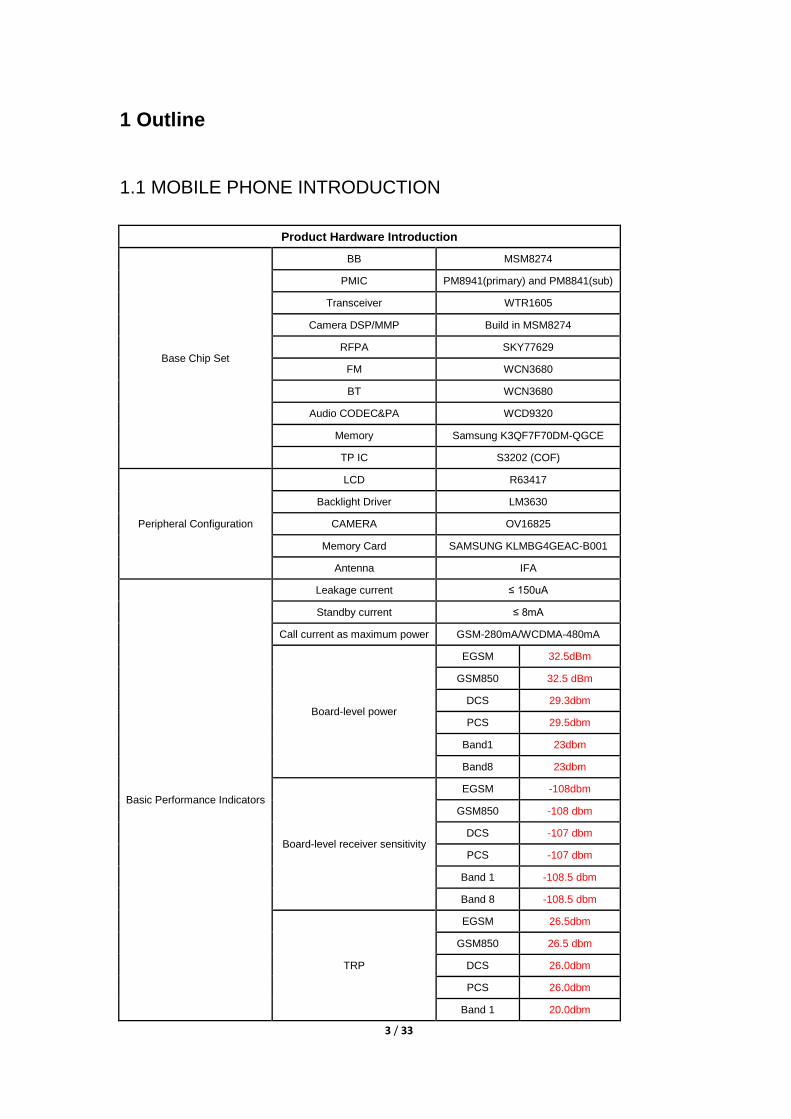
1 Outline
1.1 MOBILE PHONE INTRODUCTION
Product Hardware Introduction
Base Chip Set
BB MSM8274
PMIC PM8941(primary) and PM8841(sub)
Transceiver WTR1605
Camera DSP/MMP Build in MSM8274
RFPA SKY77629
FM WCN3680
BT WCN3680
Audio CODEC&PA WCD9320
Memory Samsung K3QF7F70DM-QGCE
TP IC S3202 (COF)
Peripheral Configuration
LCD R63417
Backlight Driver LM3630
CAMERA OV16825
Memory Card SAMSUNG KLMBG4GEAC-B001
Antenna IFA
Basic Performance Indicators
Leakage current ≤ 150uA
Standby current ≤ 8mA
Call current as maximum power GSM-280mA/WCDMA-480mA
Board-level power
EGSM 32.5dBm
GSM850 32.5 dBm
DCS 29.3dbm
PCS 29.5dbm
Band1 23dbm
Band8 23dbm
Board-level receiver sensitivity
EGSM -108dbm
GSM850 -108 dbm
DCS -107 dbm
PCS -107 dbm
Band 1 -108.5 dbm
Band 8 -108.5 dbm
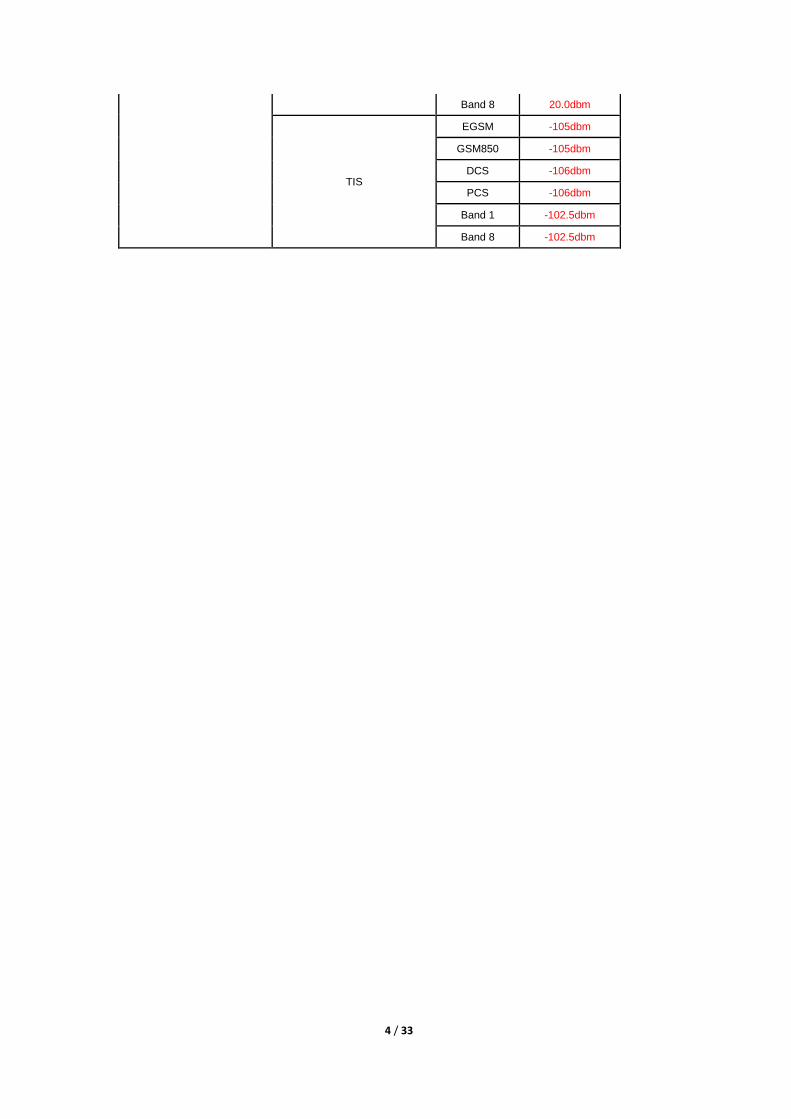
TRP
EGSM 26.5dbm
GSM850 26.5 dbm
DCS 26.0dbm
PCS 26.0dbm
Band 1 20.0dbm
4 / 33
Band 8 20.0dbm
TIS
EGSM -105dbm
GSM850 -105dbm
DCS -106dbm
PCS -106dbm
Band 1 -102.5dbm
Band 8 -102.5dbm
5 / 33
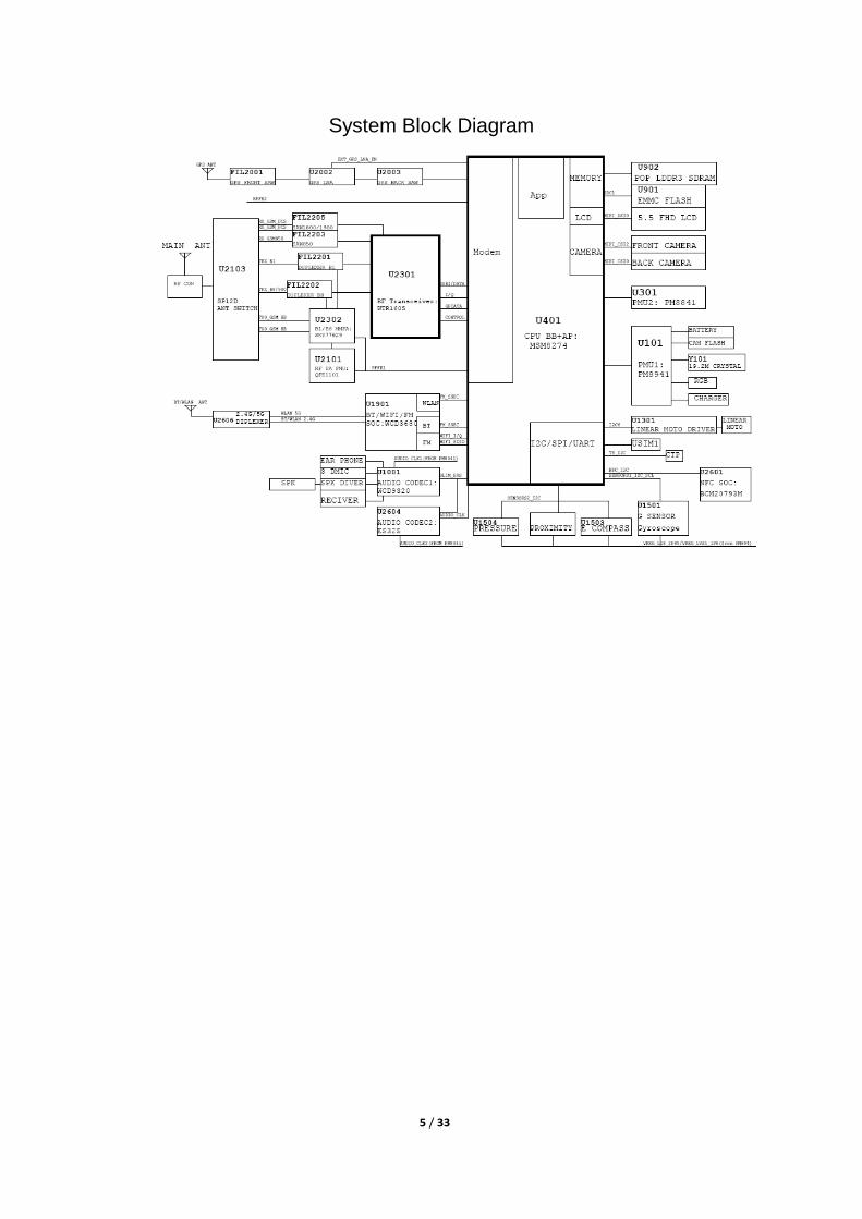
System Block Diagram

6 / 33
1.2 Motherboard Components Distribution
7 / 33
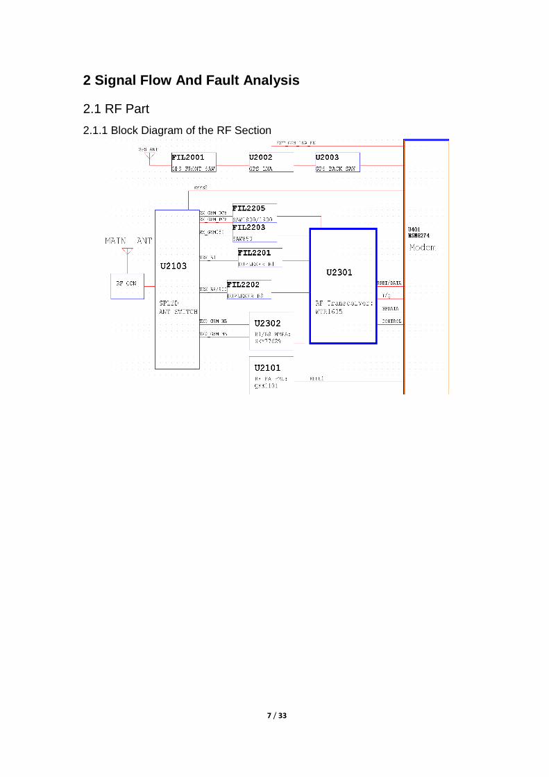
2 Signal Flow And Fault Analysis
2.1 RF Part
2.1.1 Block Diagram of the RF Section

8 / 33
RF part Diagram
RF and BB interface Diagram

9 / 33
2.1.2 Signal Flow OF the RF Transmitting Part
2.1.2.1 Receiving and Transmit Path
Receiving
Transmit

10 / 33
2.1.2.2 Maintenance Procedures of the Transmitting Part
(NO launch) Connect the PC and the phone with maintenance line,
then making the phone into the RF state with QRCT software
Check Transceiver to
see if IO signals exist.
Check the PA output to
see if there is RF signal
Y
Check CPU N
Check RF coaxial
switch or matching
network.
Y Check the
Transceiver to see if
there is RF signal
N
Check U2101-VPA
have the correct
Replace PA
Y
Check CPU
Y
Check Transceiver if
SSBI,GP_DATA,power
have the correct
N
N
N
N Y
Replace Transceiver
Check RFFE
signal have
the correct
N
Check
U2101

11 / 33
2.1.3 Signal Flow of the Receiving Part
2.1.3.1 Maintenance Procedures of the Receiving Part
No receiving
Start the META software to connect the PC and the phone,making the phone into the receiving state.
Signal generator is also adjusted to the correspond CH. And signal lines connected to the phone.
Transceiver has Check CPU Y
Transceiver has received
signal?
N
Check Transceiver SSBI,
GP_DATA are correct ?
Check CPU
N
Whether the voltage
of the transceiver is
normal? Whether
19.2MHZ is normal?
Y
Check the
corresponding power
supply and 19.2MHZ
resulting circuit
N
Replace transceiver
Y
Filter or duplex
has received
signal?
N
Check to see if there has
signal in the matching circuit
between fiter/duplex and ANT
N
Check to see if there has
signal in the matching
circuit between PA and
transceiver
Y
Y

12 / 33
2.2 Baseband Part
2.2.1 Block Diagram of the Baseband Part
13 / 33
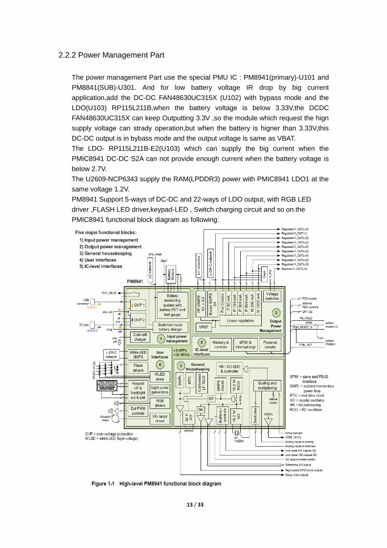
2.2.2 Power Management Part
The power management Part use the special PMU IC : PM8941(primary)-U101 and
PM8841(SUB)-U301. And for low battery voltage IR drop by big current
application,add the DC-DC FAN48630UC315X (U102) with bypass mode and the
LDO(U103) RP115L211B,when the battery voltage is below 3.33V,the DCDC
FAN48630UC315X can keep Outputting 3.3V ,so the module which request the hign
supply voltage can strady operation,but when the battery is higner than 3.33V,this
DC-DC output is in bybass mode and the output voltage is same as VBAT.
The LDO- RP115L211B-E2(U103) which can supply the big current when the
PMIC8941 DC-DC S2A can not provide enough current when the battery voltage is
below 2.7V.
The U2609-NCP6343 supply the RAM(LPDDR3) power with PMIC8941 LDO1 at the
same voltage 1.2V.
PM8941 Support 5-ways of DC-DC and 22-ways of LDO output, with RGB LED
driver ,FLASH LED driver,keypad-LED , Switch charging circuit and so on.the
PMIC8941 functional block diagram as following:

14 / 33
The SUB PMIC 8841 support 8-ways of DC-DC, power the platform big current
module, such as: Quad-Krait applications processor system, the PMIC8841
functional block diagram as following:
2.2.2.1 The Whole Power Supply System
PMIC8941 DC-DC list:
PMIC8841 DC-DC list:
15 / 33
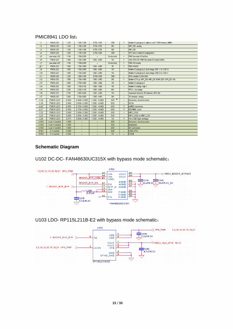
PMIC8941 LDO list:
Schematic Diagram
U102 DC-DC- FAN48630UC315X with bypass mode schematic:
U103 LDO- RP115L211B-E2 with bypass mode schematic:
16 / 33
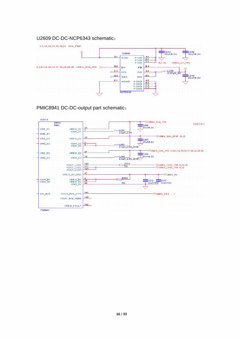
U2609 DC-DC-NCP6343 schematic:
PMIC8941 DC-DC-output part schematic:

17 / 33
PMIC8941 LCD backlight driver(Not used,this phone used external LCD
backlight driver for better performance),RGB-LED driver and camera FLAH
LED driver schematic:
PMIC8841 DC-DC-output part schematic:

18 / 33
PMIC8941 LDO-output part schematic:
2.2.3 Audio Part
2.2.3.1 Audio CODEC Circuit
The phone has used a special CODEC chip—WCD9320.In addition, It has use a
unique chip—ES325.The ES325 chip which is produced by Audience company have
strong effect in decrease noise. If you meet some problem about Audio Part, you can
check audio device like Mic, Speaker, Receiver firstly. Then you can find CODEC chip
problem. Finally, you can check CPU problem.
Audio system circuit:

19 / 33
Es325:
Use YDA168 for audio PA
20 / 33
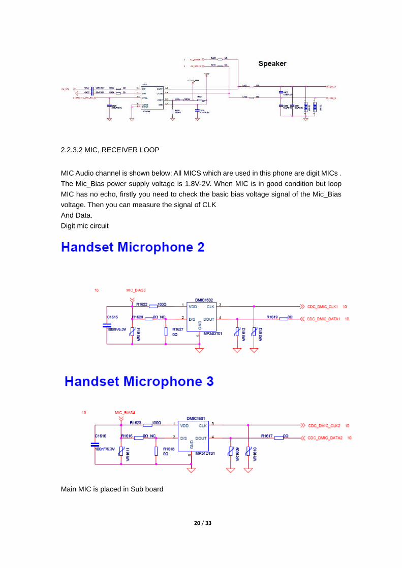
2.2.3.2 MIC, RECEIVER LOOP
MIC Audio channel is shown below: All MICS which are used in this phone are digit MICs .
The Mic_Bias power supply voltage is 1.8V-2V. When MIC is in good condition but loop
MIC has no echo, firstly you need to check the basic bias voltage signal of the Mic_Bias
voltage. Then you can measure the signal of CLK
And Data.
Digit mic circuit
Main MIC is placed in Sub board

21 / 33
Receiver units
2.2.3.3 HEADSET LOOP
Headset loop units are placed on FPC, the Motherboard headset LOOP drive the FPC
directly through CN1501.Filter and ESD protected network, are also placed on FPC.
When headset is abnormal, you can check headset problem, FPC connector, and codec,
cpu chip As shown below:

22 / 33
2.2.3..4 Speaker part
The speaker part is placed on sub board. Main board using CN1401 connect with sub
board. The chip IC-YDA168 is used to drive Speaker for strong effect. If you some
problem about speaker, firstly you should check speak, FPC connector problems. Then
check chip problems like YDA168, CODEC and CPU.
23 / 33
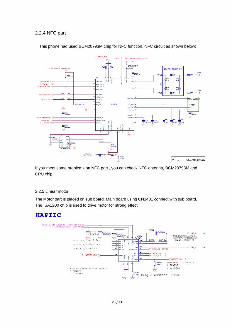
2.2.4 NFC part
This phone had used BCM20793M chip for NFC function. NFC circuit as shown below:
If you meet some problems on NFC part , you can check NFC antenna, BCM20793M and
CPU chip
2.2.5 Linear motor
The Motor part is placed on sub board. Main board using CN1401 connect with sub board.
The ISA1200 chip is used to drive motor for strong effect.

24 / 33
2.2.6 Analysis of the Display Module circuit
Display module use the 5.5"TN LCD, which including 4 pairs MIPI differential bus mode.
All of commend and data go through the MIPI differential bus mode except the reset
signal.
The LED Backlight driver use LM3630 IC, the circuit as shown below:
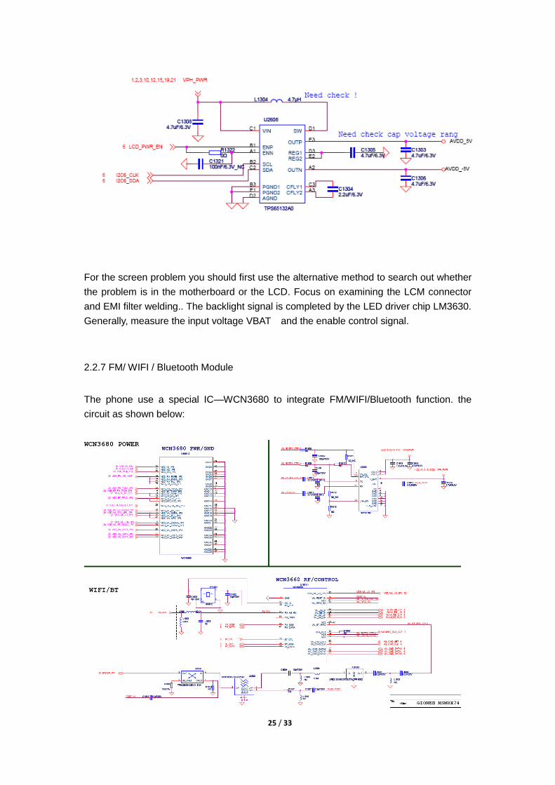
25 / 33
For the screen problem you should first use the alternative method to search out whether
the problem is in the motherboard or the LCD. Focus on examining the LCM connector
and EMI filter welding.. The backlight signal is completed by the LED driver chip LM3630.
Generally, measure the input voltage VBAT and the enable control signal.
2.2.7 FM/ WIFI / Bluetooth Module
The phone use a special IC—WCN3680 to integrate FM/WIFI/Bluetooth function. the
circuit as shown below:

26 / 33
If You want to resolve FM problem you can check the headphone circuit firstly, then
check WCN3680,CPU circuit. WIFI and Bluetooth use a same antenna.
2.2.8 Camera Module
The module uses 16 million pixel AF camera as the main camera, 8 million pixel camera
as the sub camera. Through the connector and the baseband chip (the main camera
series EMI devices) directly connected.
The Camera Interface Circuit as show below:
The Camera Power Supply Circuit
The DOVDD supply 1.8V to Camera IO interface voltage, AVDD supply 2.8V analog
voltage. DVDD supply 1.2V for core voltage ,VAF supply 2.8v for motor voltage.
Flash driver use PMIC8941
27 / 33
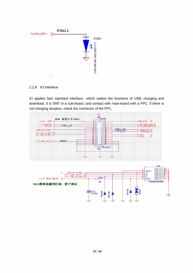
2.2.9 IO Interface
IO applies 5pin standard interface,which realize the functions of USB, charging and
download. It is SMT in a sub-board, and contact with main-board with a FPC. If there is
not charging situation, check the connector of the FPC.
28 / 33
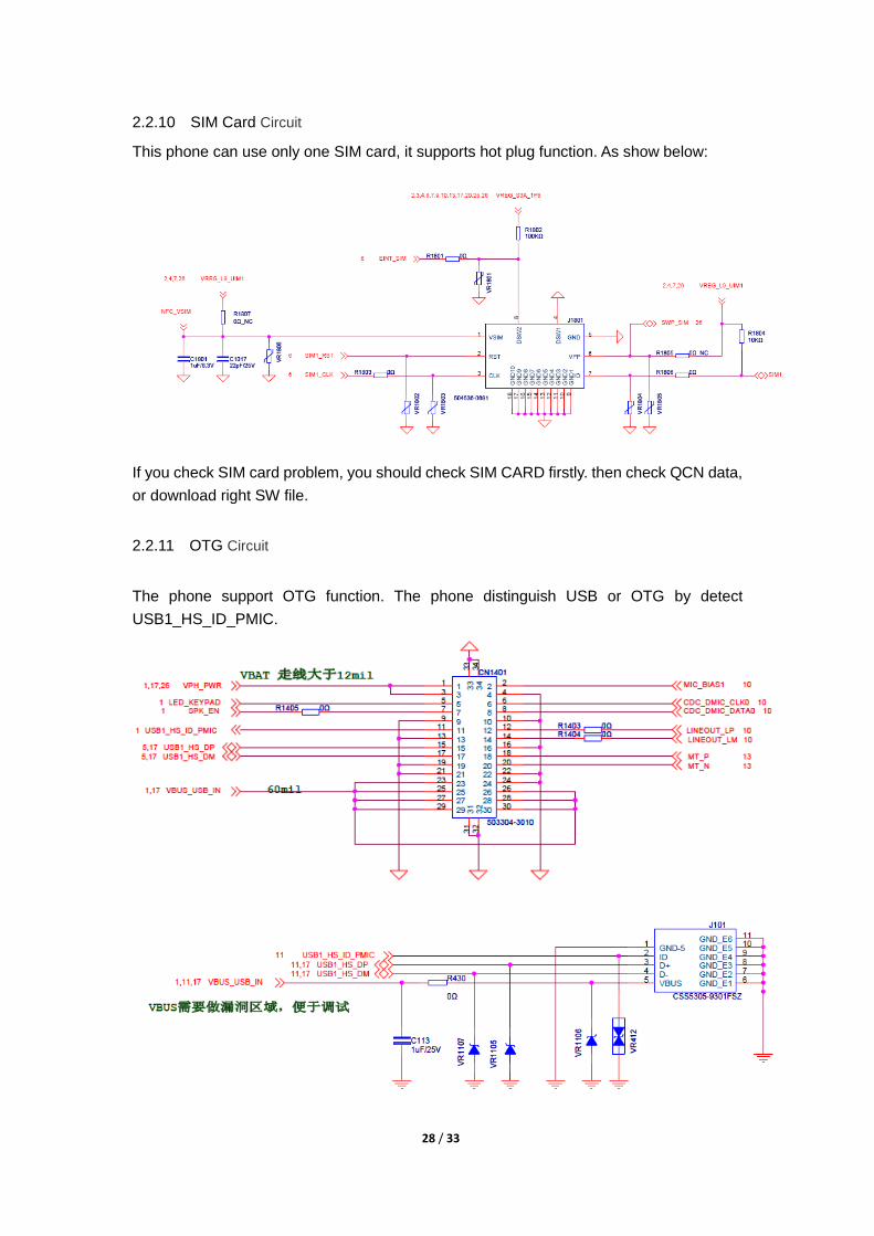
2.2.10 SIM Card Circuit
This phone can use only one SIM card, it supports hot plug function. As show below:
If you check SIM card problem, you should check SIM CARD firstly. then check QCN data,
or download right SW file.
2.2.11 OTG Circuit
The phone support OTG function. The phone distinguish USB or OTG by detect
USB1_HS_ID_PMIC.
29 / 33
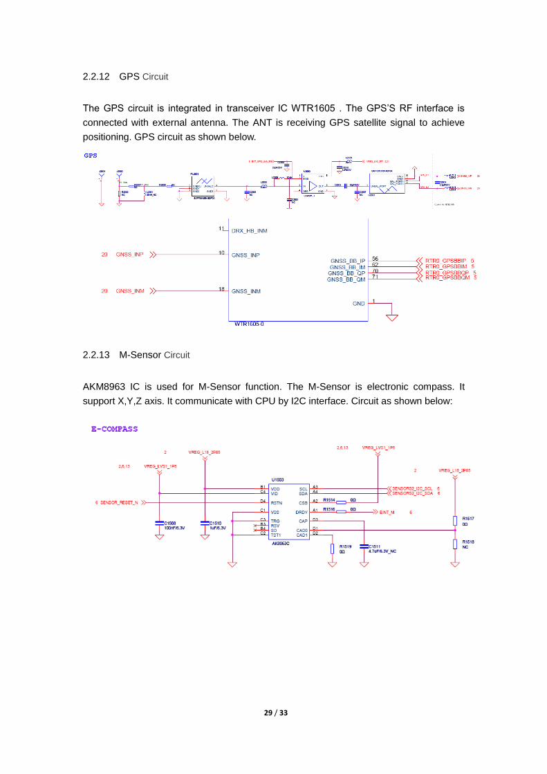
2.2.12 GPS Circuit
The GPS circuit is integrated in transceiver IC WTR1605 . The GPS’S RF interface is
connected with external antenna. The ANT is receiving GPS satellite signal to achieve
positioning. GPS circuit as shown below.
2.2.13 M-Sensor Circuit
AKM8963 IC is used for M-Sensor function. The M-Sensor is electronic compass. It
support X,Y,Z axis. It communicate with CPU by I2C interface. Circuit as shown below:
30 / 33
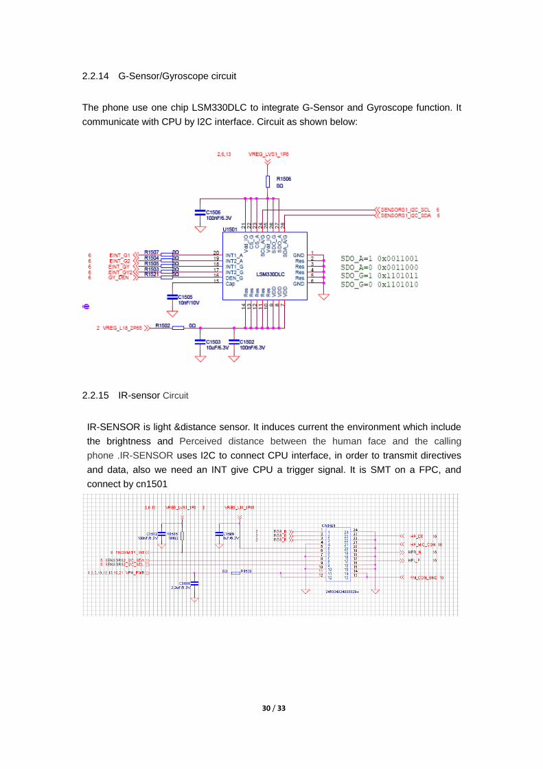
2.2.14 G-Sensor/Gyroscope circuit
The phone use one chip LSM330DLC to integrate G-Sensor and Gyroscope function. It
communicate with CPU by I2C interface. Circuit as shown below:
2.2.15 IR-sensor Circuit
IR-SENSOR is light &distance sensor. It induces current the environment which include
the brightness and Perceived distance between the human face and the calling
phone .IR-SENSOR uses I2C to connect CPU interface, in order to transmit directives
and data, also we need an INT give CPU a trigger signal. It is SMT on a FPC, and
connect by cn1501
31 / 33
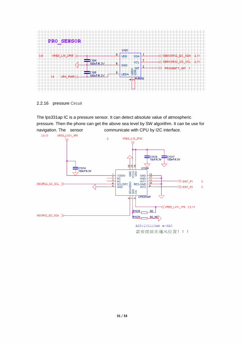
2.2.16 pressure Circuit
The lps331ap IC is a pressure sensor. It can detect absolute value of atmospheric
pressure. Then the phone can get the above sea level by SW algorithm. It can be use for
navigation. The sensor communicate with CPU by I2C interface.

32 / 33
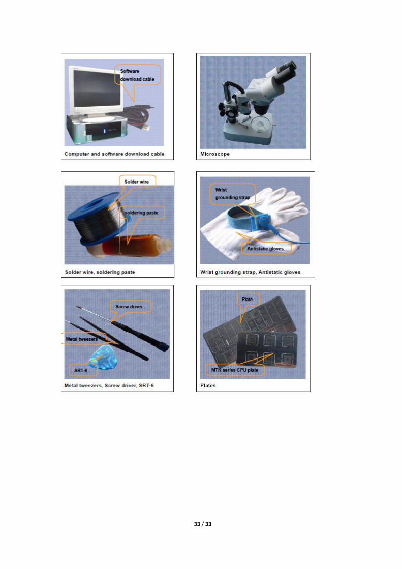
3. Disassembly and assembly service Tools
33 / 33