leveraging power leadership at 28 nm with xilinx 7 … · the xilinx power tools ... leveraging...
TRANSCRIPT
WP436 (v1.1) January 5, 2015 www.xilinx.com 1
© Copyright 2013–2015 Xilinx, Inc. Xilinx, the Xilinx logo, Artix, ISE, Kintex, Spartan, Virtex, Vivado, Zynq, and other designated brands included herein are trademarks of Xilinx in the United States and other countries. PCI, PCIe, and PCI Express are trademarks of PCI-SIG and used under license. All other trademarks are the property of their respective owners.
Power is increasingly becoming a key differentiatorfor the creation of next-generation semiconductorproducts at deep sub-micron geometries that requiretight thermal and power budgets. The key challengebeing faced by many manufacturers of electronicssystems is the ability to accurately estimate theirdesigns’ power budgets — and then achieve thosebudget targets with power optimization solutions.
Based on a solid foundation of power understandingand planning, Xilinx has delivered, with the 28 nm7 series FPGAs, the most effective power solutions inthe industry, providing 28HPL process benefits,stable power specifications, ready parts availability,low-power solutions, and best-in-class power tools.
The Xilinx power tools’ estimation and optimizationmethods are showcased using design suite analysison actual customer designs, highlighting the powertools’ capabilities.
White Paper: 7 Series FPGAs
WP436 (v1.1) January 5, 2015
Leveraging Power Leadership at 28 nm with Xilinx 7 Series FPGAs
By: Matt Klein and Srinivasa Kolluri
2 www.xilinx.com WP436 (v1.1) January 5, 2015
Introduction
IntroductionChanging market demands and the increasing complexity of systems motivate customers to achieve the best possible performance at each technology node. Faced with shorter product life spans and compressed time-to-market requirements, FPGAs are a viable, highly attractive customer production choice. Power consumption has become one of the primary concerns for customers migrating from ASSPs/ASICs to FPGAs. Xilinx® FPGAs have consistently delivered innovative low-power solutions by researching and implementing strategies based on an ideal mix of low-power architectures, process improvements, voltage-scalable products, and power-optimization techniques.
As the only 28 nm FPGAs fabricated on a high-performance, low-power process (28HPL), 7 series devices offer lower total power consumption and superior performance per watt compared to competing solutions. Architectural and block-level innovations unique to Xilinx add to the power advantages at every level. In addition, to ensure a smooth production rollout, 7 series FPGAs provide credible power estimation and optimization, stable power specifications, and robust availability of lower-power parts.
Process Technology: 28HPL Process BenefitsThe 28HPL process technology has lower leakage and eliminates the need for complex and expensive static power management schemes in the FPGA design. The larger design headroom (voltage headroom) in the HPL process allows the choice of operating VCC at a wider range of values and enables a flexible power/performance strategy—which is not possible with the 28HP process. The benefits of 28HPL also include:
• High-Performance Mode (VCC = 1.0V): 28HPL offers comparable performance to 28HP at lower static power in the performance target range for FPGAs.
• Low-Power Modes (VCC = 0.95V, 0.9V): 28HPL offers 65% lower static power than 28HP. The headroom in 28HPL allows Xilinx to offer multiple low power speed grades (-1LI, -2LI, and -2LE). Significant power savings are made possible with the -2LI which offers full -2 performances along with 10% savings on dynamic power and 40% savings on static power. The -1LI delivers the absolute lowest static power with -1 performance along with 10% savings on dynamic power.
The net result is that competing FPGAs built with the 28HP process have no performance advantage over 7 series FPGAs, while some of the competing FPGAs come with the severe penalty of >2X the static power and have challenges in reducing leakage. See WP389, Lower Power at 28 nm with Xilinx 7 Series FPGAs.
Stable Power SpecificationsEvery 7 series device is tested to published maximum static power specifications to ensure power consumption meets or is typically below expectations. Competing 28 nm solutions have had to raise static power specifications near or after production, or simply failed to report maximum static power altogether, forcing designers to re-evaluate system demands.
The 7 series devices have a stable specification for core operating voltage, and Xilinx has delivered on providing standard production devices that meet published static
Process Technology: 28HPL Process Benefits
WP436 (v1.1) January 5, 2015 www.xilinx.com 3
power specifications. At the 28 nm node, Xilinx’s primary competitor had to raise the core voltage specification—as noted in their production errata. The revised power specifications result in a 20% increase in static power for their FPGAs. In each of their subsequent power estimator tool releases, they have raised the static power further, to a range of 30% higher compared to their original power specification. The same issue also exists in their mid-range offering.
In contrast, Xilinx has invested a great deal of time and resources to ensure that the power specifications published when the product is announced do not change throughout the production time frame. This allows customers to plan their board design confidently without worrying about inaccurate power estimates and performance imbalances. See Table 1.
Reliable Thermal SolutionThe demand to achieve higher performance by moving to smaller process nodes and packing more functionality into FPGAs places a tight constraint on power budgets. Power is directly related to thermal considerations because heat dissipated in the FPGA increases with higher power consumption. Thermal concerns are also linked to product reliability because every 10°C rise in temperature doubles the failure rate. Xilinx has extensively researched device packaging to reduce thermal resistance and help power dissipation. Reducing static power enables FPGA operation at a lower junction temperature, addressing thermal concerns and improving performance. Xilinx has a major advantage over the competition because the 28 nm HPL process, when combined with the flexible low-power options, enables significant static power reduction. This helps keep the junction temperature low and within the operating range of the device.
The very low static power afforded by the 7 series 28HPL process offers several benefits in a high-temperature environment. The data shown in Figure 1 compares the design's static power (including transceiver power) when implemented on a Xilinx 28HPL device with 410K logic cells vs. the competition's 28HP device with 457K equivalent logic cells. The difference in static power at a fixed junction temperature (Tj) is important not only from the point of view of total power but also from the perspective of operating temperature. The device with higher static power has a greater challenge of maintaining the correct operating temperature because any incremental change in power consumption can cause the device temperature to exceed the specified operating temperature.
Table 1: Maximum Static Power Specification Changes Near or After Entering Production
28 nm Family Xilinx Competitor
Low End No Change 10–20% Increase
Mid-range No Change ~50% Increase
High End No Change ~10-30% Increase
Notes: 1. Typical static power for the competitor’s low-end 28 nm device increased by 100% after
production data was released in XPE.

4 www.xilinx.com WP436 (v1.1) January 5, 2015
Process Technology: 28HPL Process Benefits
Static power is highly dependent on die temperature, and Xilinx provides a complete thermal solution that helps keep the FPGA in the proper operating range.
The graph in Figure 2 plots junction temperature vs. ambient temperature for the 7 series standard- and low-power devices with 690K logic cells and compares them to the competitor's parts with 622K equivalent logic cells. The same design was implemented on all the parts with similar logic cell count. The design consisted of DDR3 interfaces, block RAM, LUTs, and 10G transceivers. The graph shows that in spite of using a larger device and operating at the same thermal resistance, the Xilinx devices have a much better maximum ambient temperature due to low static power. The design using the Xilinx device can operate at a higher ambient temperature without exceeding the maximum junction temperature of 100°C. In other words, lower static power allows the design to operate over wider environmental conditions. The ability to operate at 50–60°C ambient temperature while maintaining the 100°C junction temperature is essential in many applications, such as wired communications designs operating in a rack-style environment.
X-Ref Target - Figure 1
Figure 1: Xilinx 28HPL and Competitor’s 28HP Max Static Power vs. Tj
X-Ref Target - Figure 2
Figure 2: Virtex-7 VX690T FPGA and Competitor’s Nearest 28HP Devices, Same Design
Junction Temperature (Tj)
Sta
tic P
ower
(W
)
7.2W
Xilinx 28HPL Static Power (Standard I-grade)
Competitor’s 28HP Static Power
3.6W
+3.6W
WP436_01_080713
20
18
16
14
13
10
8
6
4
2
0–40°C –20°C 0°C 20°C 40°C 60°C 80°C 100°C 120°C
Ambient Temperature
Junction vs. Ambient Temperature for ThetaJA=1.4C/W
Junc
tion
Tem
pera
ture 32.1°C
Xilinx 7 series devices can operate at higher ambient temperature withoutexceeding max junction temperature.
38.0
°C45
.1°C
52.2
°C
54.0°C
Virtex-7 VX690T -2L (1V) Virtex-7 VX690T -2I (1V) Competitor‘s 28HP -2L/-3L (0.85V)Competitor’s 28HP -3/-4 (0.85V)Competitor’s 28HP -2 (0.9V)
WP436_02_080713
120°C
100°C
80°C
60°C
40°C
20°C
0°C0°C 20°C 40°C 60°C 80°C 100°C

Process Technology: 28HPL Process Benefits
WP436 (v1.1) January 5, 2015 www.xilinx.com 5
Available Device Power OptionsXilinx offers voltage scaling options, which is another benefit made possible by the headroom gained with the 28HPL process. Low-end FPGAs can operate at three core voltages: 1.0V, 0.95V, and 0.9V. This is similar to the power strategy first introduced in Virtex®-6 and Spartan®-6 devices. FPGAs that can run at 1.0V, 0.95V, and 0.9V are designated -2L, based on their speed grade at 1.0V. Their performance is identical to that of a -2 speed grade at 1.0V and 0.95V, and less than -1 when run at 0.9V—but the L signifies lower static power and low voltage capable operation.
At 0.95V, the voltage drop alone in these FPGAs offers a significant static power reduction. The voltage drop might also reduce performance—but Xilinx screens these -2L devices for speed and a tighter leakage specification compared to the standard FPGAs. Wireless applications absolutely require parts that can meet I grade temperature requirements along with meeting -2 speed grade performance. The -2LI devices offered by Xilinx meet both the temperature and speed requirements for a wide range of AVB, wireless, and industrial applications, and also help mitigate thermal design constraints by reducing the static leakage.This screening method yields a 55% reduction in static power at worst case process compared to the standard speed grade devices.
Xilinx chooses only the lower leakage and higher performance FPGAs to become -2L devices, as shown in Table 2.
FPGAs that can run at 0.95V are designated -1LI based on their speed grade at 1.0V. The I-grade provides the much wider temperature range for industrial, aerospace and defense, and other applications, which work well for -1 performance. However, these applications are also thermally constrained (and hence power constrained) due to form factor. Because of the relative lower performance, some of these applications are battery based, where the primary power component is static power. The L signifies lower static power and low voltage capable operation. At 0.95V, the voltage drop alone in these devices offers static power reduction and Xilinx further screens these -1LI devices for speed and a tighter leakage specification compared to the standard FPGAs. Xilinx chooses only the lower leakage and higher performance FPGAs to become -1LI devices.This screening method yields a 65% reduction in static power at worst case process compared to the standard speed grade and commercial temperature range devices, and 10% lower dynamic power without any drop in performance.
Table 2: Comparison of Reduced Static Power Device Options vs C-grade Devices
Low End C-Grade Devices -2LE (1.0V) -2LE(0.9V) -2LI(0.95V) -1LI(0.95V)
VCCINT 1.0V 1.0V 0.9V 0.95V 0.95V
Static Power Nominal –45% –55% –58% –65%
Dynamic Power Nominal Nominal –20% –10% –10%
Performance -1, -2 -2 < -1 -2 -1
6 www.xilinx.com WP436 (v1.1) January 5, 2015
Process Technology: 28HPL Process Benefits
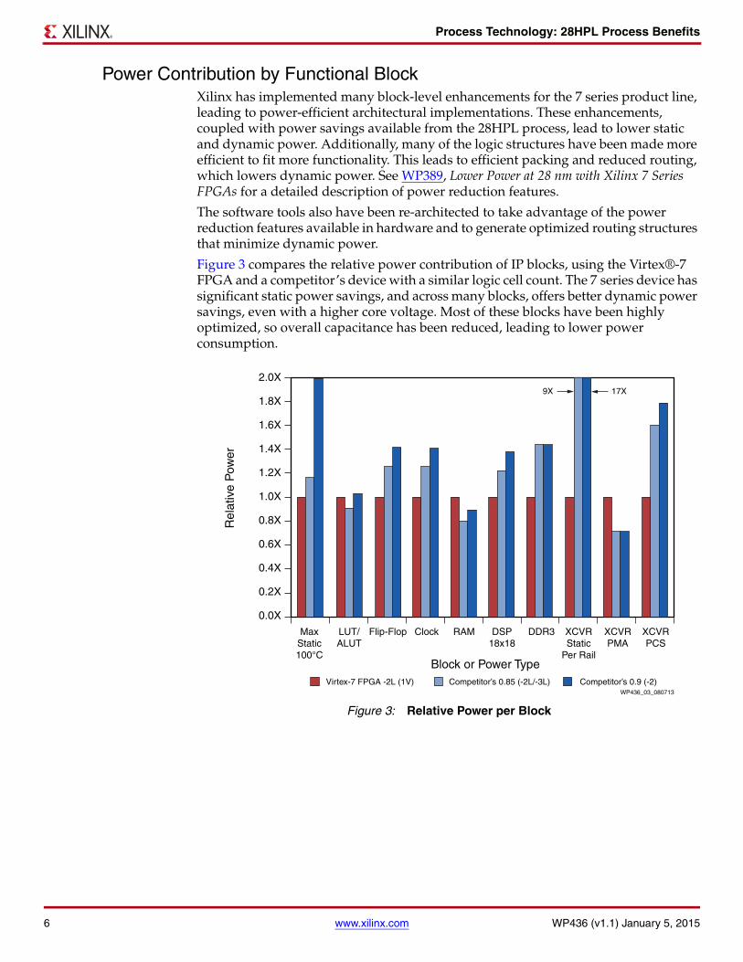
Power Contribution by Functional Block Xilinx has implemented many block-level enhancements for the 7 series product line, leading to power-efficient architectural implementations. These enhancements, coupled with power savings available from the 28HPL process, lead to lower static and dynamic power. Additionally, many of the logic structures have been made more efficient to fit more functionality. This leads to efficient packing and reduced routing, which lowers dynamic power. See WP389, Lower Power at 28 nm with Xilinx 7 Series FPGAs for a detailed description of power reduction features.
The software tools also have been re-architected to take advantage of the power reduction features available in hardware and to generate optimized routing structures that minimize dynamic power.
Figure 3 compares the relative power contribution of IP blocks, using the Virtex®-7 FPGA and a competitor’s device with a similar logic cell count. The 7 series device has significant static power savings, and across many blocks, offers better dynamic power savings, even with a higher core voltage. Most of these blocks have been highly optimized, so overall capacitance has been reduced, leading to lower power consumption. X-Ref Target - Figure 3
Figure 3: Relative Power per Block
Block or Power Type
Rel
ativ
e P
ower
Virtex-7 FPGA -2L (1V) Competitor’s 0.85 (-2L/-3L) Competitor’s 0.9 (-2)
17X9X
WP436_03_080713
2.0X
1.8X
1.6X
1.4X
1.2X
1.0X
0.8X
0.6X
0.4X
0.2X
0.0X
MaxStatic100°C
LUT/ALUT
Flip-Flop Clock RAM DSP18x18
DDR3 XCVRStatic
Per Rail
XCVRPMA
XCVRPCS
Credible Power Estimation and Optimization
WP436 (v1.1) January 5, 2015 www.xilinx.com 7
Credible Power Estimation and OptimizationMeeting system power, thermal, and reliability requirements starts with credible power estimation and optimization.
Increasing power budgets are prompting designers to consider power estimation very early in the board design process. Having credible power estimates in the early stages of design affects decisions related to the board’s thermal budget, including heatsink selection, airflow, and board material.
Accurate, highly credible power estimation also leads the designer to select the right power supplies for the design and the other board components in terms of their thermal profiles. Xilinx invested heavily in state-of-the-art resources that make it possible to deliver highly accurate power estimation through both the Xilinx Power Estimator (XPE) and the Vivado® Design Suite. XPE helps generate power estimates that can simplify device selection and board development. Early power estimates can also help the board designer explore alternative resource implementations if early design numbers exceed the power budget.
Overall, the Vivado® Design Suite performs detailed power estimation at all stages of the design, employing an innovative power optimization engine that identifies unnecessarily high power paths and ultimately delivers a significantly reduced power consumption profile that falls credibly within the power consumption budget— without impacting performance.
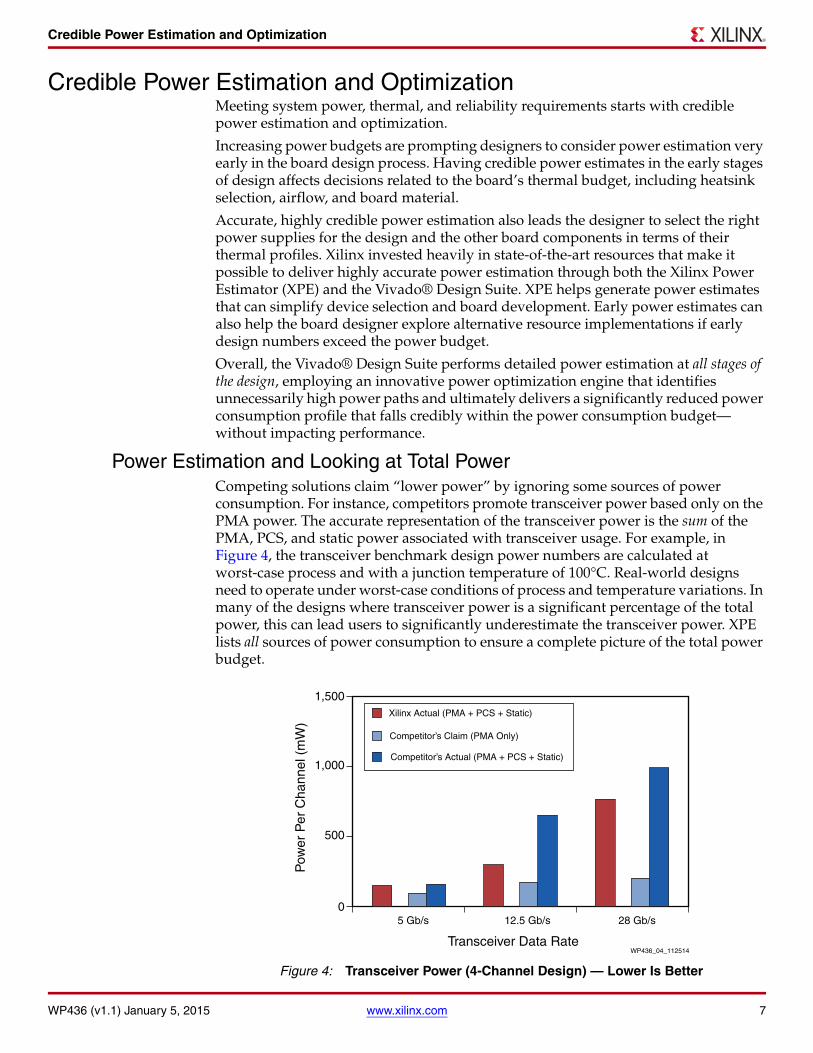
Power Estimation and Looking at Total PowerCompeting solutions claim “lower power” by ignoring some sources of power consumption. For instance, competitors promote transceiver power based only on the PMA power. The accurate representation of the transceiver power is the sum of the PMA, PCS, and static power associated with transceiver usage. For example, in Figure 4, the transceiver benchmark design power numbers are calculated at worst-case process and with a junction temperature of 100°C. Real-world designs need to operate under worst-case conditions of process and temperature variations. In many of the designs where transceiver power is a significant percentage of the total power, this can lead users to significantly underestimate the transceiver power. XPE lists all sources of power consumption to ensure a complete picture of the total power budget.X-Ref Target - Figure 4
Figure 4: Transceiver Power (4-Channel Design) — Lower Is Better
Transceiver Data Rate
Pow
er P
er C
hann
el (
mW
)
Xilinx Actual (PMA + PCS + Static)
Competitor’s Claim (PMA Only)
Competitor’s Actual (PMA + PCS + Static)
WP436_04_112514
1,500
5 Gb/s 12.5 Gb/s 28 Gb/s
1,000
500
0
8 www.xilinx.com WP436 (v1.1) January 5, 2015
Credible Power Estimation and Optimization
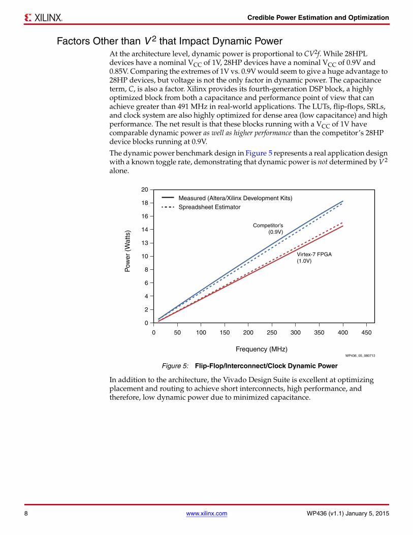
Factors Other than V 2 that Impact Dynamic PowerAt the architecture level, dynamic power is proportional to CV2f. While 28HPL devices have a nominal VCC of 1V, 28HP devices have a nominal VCC of 0.9V and 0.85V. Comparing the extremes of 1V vs. 0.9V would seem to give a huge advantage to 28HP devices, but voltage is not the only factor in dynamic power. The capacitance term, C, is also a factor. Xilinx provides its fourth-generation DSP block, a highly optimized block from both a capacitance and performance point of view that can achieve greater than 491 MHz in real-world applications. The LUTs, flip-flops, SRLs, and clock system are also highly optimized for dense area (low capacitance) and high performance. The net result is that these blocks running with a VCC of 1V have comparable dynamic power as well as higher performance than the competitor’s 28HP device blocks running at 0.9V.
The dynamic power benchmark design in Figure 5 represents a real application design with a known toggle rate, demonstrating that dynamic power is not determined by V2 alone.
In addition to the architecture, the Vivado Design Suite is excellent at optimizing placement and routing to achieve short interconnects, high performance, and therefore, low dynamic power due to minimized capacitance.
X-Ref Target - Figure 5
Figure 5: Flip-Flop/Interconnect/Clock Dynamic Power
Frequency (MHz)
Pow
er (
Wat
ts)
Measured (Altera/Xilinx Development Kits)
Spreadsheet Estimator
WP436_05_080713
20
18
16
14
13
10
8
6
4
2
0
0 50 100 150 200 250 300 350 400 450
Competitor’s(0.9V)
Virtex-7 FPGA(1.0V)
Vivado Design Suite Power Analysis and Optimization
WP436 (v1.1) January 5, 2015 www.xilinx.com 9
Vivado Design Suite Power Analysis and OptimizationThe Vivado Design Suite offers powerful and flexible power analysis, including:
• Graphic and text views of power consumption in a user design• Advanced cross-probing capabilities from the power report to the user design• Ability to accept SAIF files for more detailed power estimation• Support for “What if” scenarios to further reduce power
The Vivado Design Suite offers customers the convenience of performing power estimation at all stages of the flow: post-synthesis, post-placement, and routing. The Vivado Design Suite provides the most accurate post-routing power estimate because it can estimate exact logic and routing resources by reading in the design database file. Results are displayed in an interactive summary power report and grouped by clock domain, resource type, and design hierarchy.
The Vivado Design Suite gives customers the ability to make changes to their design activity and monitor changes to the power estimate. One of the innovative features has been the addition of a cross-probing mode, which allows the user to cross-probe into the design hierarchical view from the power report. This focuses attention on the resources that are consuming high power in the design.
The Vivado Design Suite offers the flexibility of performing either a vector-based power estimation (by means of user data activity input), or a vectorless power estimation. The vectorless algorithm can predict activity at internal nodes and even estimates glitching activity. A user faced with a computing efficiency problem could choose the vectorless mode; a user looking for the most detailed estimate possible might choose the vector-based mode instead.
The Vivado Design Suite also has the ability to generate a Xilinx power estimator file that can be analyzed by XPE, storing various parameters such as environment information, device usage, and design activity. This feature is very useful when the user suspects the power budget might be exceeded and that optimization alone might not solve the problem. The user can explore different mapping, gating, or other strategies after examining the XPE results.
Power Optimization Result ComparisonsThe benchmark suite shown in Table 3 comprises a collection of 28 designs carefully selected from real-world customer cases. Run on Vivado Design Suite and also on the competitor's software, the resource counts were implemented similarly in both tools. The analysis of the results from the design suite revealed that the competitor's software barely showed a reduction in power. In cases where power was optimized, performance was adversely impacted significantly.
Table 3: Design Tool Power Optimization Analysis (Average of 28 Designs)
Power Optimization Xilinx Competitor
Normal (Default)Reported Power Reduction 7.5% 1%
Performance Change 0% –2%
Extra EffortReported Power Reduction 18% 12%
Performance Change –1% –9%
10 www.xilinx.com WP436 (v1.1) January 5, 2015
Vivado Design Suite Power Analysis and Optimization
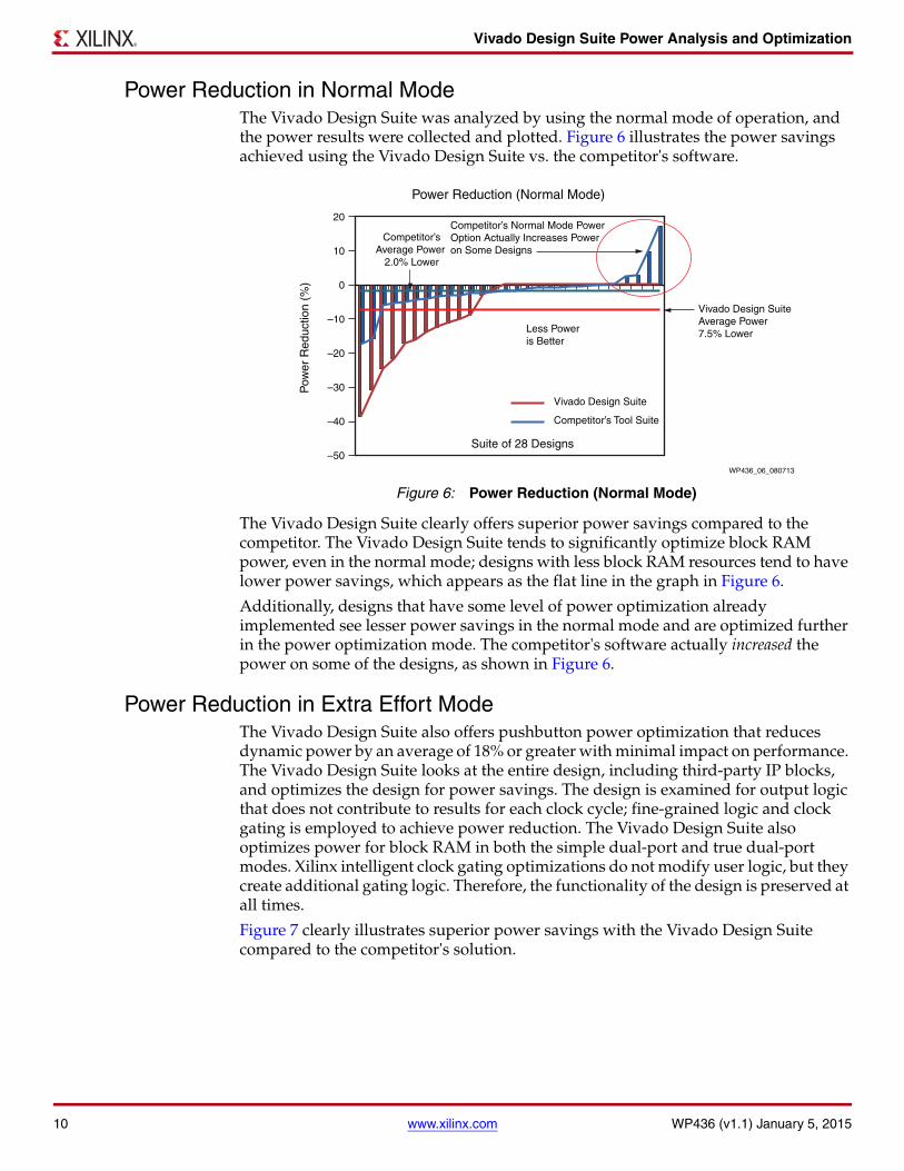
Power Reduction in Normal ModeThe Vivado Design Suite was analyzed by using the normal mode of operation, and the power results were collected and plotted. Figure 6 illustrates the power savings achieved using the Vivado Design Suite vs. the competitor's software.
The Vivado Design Suite clearly offers superior power savings compared to the competitor. The Vivado Design Suite tends to significantly optimize block RAM power, even in the normal mode; designs with less block RAM resources tend to have lower power savings, which appears as the flat line in the graph in Figure 6.
Additionally, designs that have some level of power optimization already implemented see lesser power savings in the normal mode and are optimized further in the power optimization mode. The competitor's software actually increased the power on some of the designs, as shown in Figure 6.
Power Reduction in Extra Effort Mode The Vivado Design Suite also offers pushbutton power optimization that reduces dynamic power by an average of 18% or greater with minimal impact on performance. The Vivado Design Suite looks at the entire design, including third-party IP blocks, and optimizes the design for power savings. The design is examined for output logic that does not contribute to results for each clock cycle; fine-grained logic and clock gating is employed to achieve power reduction. The Vivado Design Suite also optimizes power for block RAM in both the simple dual-port and true dual-port modes. Xilinx intelligent clock gating optimizations do not modify user logic, but they create additional gating logic. Therefore, the functionality of the design is preserved at all times.
Figure 7 clearly illustrates superior power savings with the Vivado Design Suite compared to the competitor's solution.
X-Ref Target - Figure 6
Figure 6: Power Reduction (Normal Mode)
Power Reduction (Normal Mode)
Pow
er R
educ
tion
(%)
Competitor’sAverage Power
2.0% Lower
Competitor’s Normal Mode PowerOption Actually Increases Poweron Some Designs
WP436_06_080713
20
10
0
–10
–20
–30
–40
–50
Vivado Design SuiteAverage Power 7.5% Lower
Vivado Design Suite
Competitor’s Tool Suite
Less Poweris Better
Suite of 28 Designs

Vivado Design Suite Power Analysis and Optimization
WP436 (v1.1) January 5, 2015 www.xilinx.com 11
Performance Impact of Power OptimizationsThe Vivado Design Suite achieves power optimization with negligible performance impact, whereas the competitor's software degrades the performance significantly to achieve power optimization. FPGA high-level synthesis and routing tools inherently introduce some variance between design runs. Even the minimal performance impact of the Vivado Design Suite could be accounted for by design-run variance. The competitor's tools, by comparison, exhibit significant performance degradation — too large to be explained away as merely a symptom of run-to-run variation.
Figure 8 demonstrates that the superior optimization technique used in the Vivado Design Suite produces nearly zero performance impact, on average, compared to the nearly 10% performance degradation resulting from use of the competitor's tool.
X-Ref Target - Figure 7
Figure 7: Power Reduction (Extra Effort Mode)
Pow
er R
educ
tion
(%)
Competitor’sAverage Power Reduction: 12%
WP436_07_080713
30
20
10
0
–10
–20
–30
–40
–50
–60
Vivado Design SuiteAverage Power Reduction: 18%
Vivado Design SuiteProvides GreaterPower Reduction
Suite of 28 Designs
Vivado Design Suite
Competitor’s Tool Suite
X-Ref Target - Figure 8
Figure 8: Performance Impact of Power Optimization (Extra Effort Mode)
Per
form
ance
(%
)
Vivado Design SuiteAverage Performance Impact
1% Lower
WP436_08_080713
10
5
0
–5
–10
–15
–20
–25
Competitor’sAverage Performance Impact9% Lower
Lower Performanceis Bad
Suite of 28 Designs
Vivado Design Suite
Competitor’s Tool Suite
12 www.xilinx.com WP436 (v1.1) January 5, 2015
Xilinx 7 Series Delivers Lower Total Power
In addition, Vivado Design Suite also offers the flexibility of choosing where power optimization is applied to a coarse-grained level (i.e., to a hierarchy or clock domain) or fine-grained level (to individual registers or block RAMs) to both control and lessen the impact power optimization can have on any particular design while still allowing optimizations to occur where they do not impact timing.
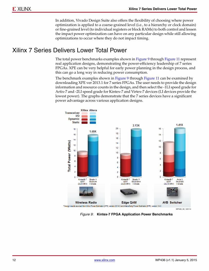
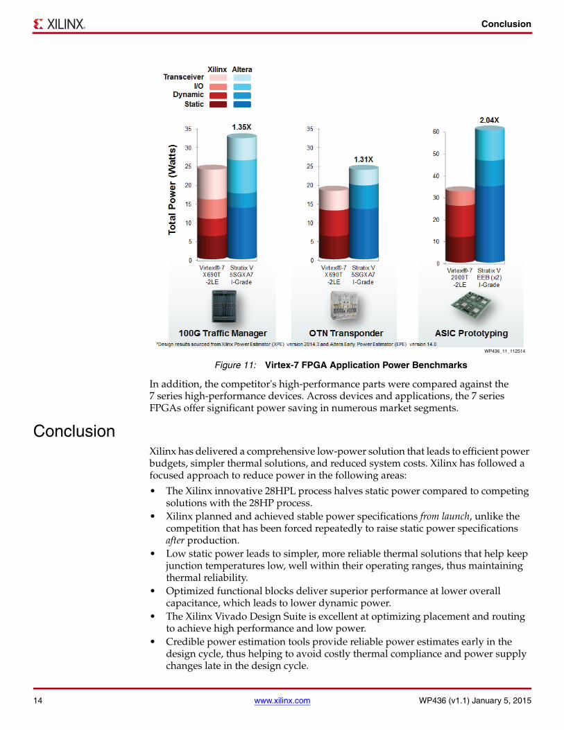
Xilinx 7 Series Delivers Lower Total Power The total power benchmarks examples shown in Figure 9 through Figure 11 represent real application designs, demonstrating the power-efficiency leadership of 7 series FPGAs. XPE can be very helpful for early power planning in the design process, and this can go a long way in reducing power consumption.
The benchmark examples shown in Figure 9 through Figure 11 can be examined by downloading XPE ver 2013.1 for 7 series FPGAs. The user needs to provide the design information and resource counts in the design, and then select the -1LI speed grade for Artix-7 and -2LI speed grade for Kintex-7 and Virtex-7 devices (LI devices provide the lowest power). The graphs demonstrate that the 7 series devices have a significant power advantage across various application designs.X-Ref Target - Figure 9
Figure 9: Kintex-7 FPGA Application Power Benchmarks
WP436_09_120114

Xilinx 7 Series Delivers Lower Total Power
WP436 (v1.1) January 5, 2015 www.xilinx.com 13
X-Ref Target - Figure 10
Figure 10: Artix-7 FPGA Application Power Benchmarks
WP436_10_112514
14 www.xilinx.com WP436 (v1.1) January 5, 2015
Conclusion
In addition, the competitor's high-performance parts were compared against the 7 series high-performance devices. Across devices and applications, the 7 series FPGAs offer significant power saving in numerous market segments.
Conclusion Xilinx has delivered a comprehensive low-power solution that leads to efficient power budgets, simpler thermal solutions, and reduced system costs. Xilinx has followed a focused approach to reduce power in the following areas:
• The Xilinx innovative 28HPL process halves static power compared to competing solutions with the 28HP process.
• Xilinx planned and achieved stable power specifications from launch, unlike the competition that has been forced repeatedly to raise static power specifications after production.
• Low static power leads to simpler, more reliable thermal solutions that help keep junction temperatures low, well within their operating ranges, thus maintaining thermal reliability.
• Optimized functional blocks deliver superior performance at lower overall capacitance, which leads to lower dynamic power.
• The Xilinx Vivado Design Suite is excellent at optimizing placement and routing to achieve high performance and low power.
• Credible power estimation tools provide reliable power estimates early in the design cycle, thus helping to avoid costly thermal compliance and power supply changes late in the design cycle.
X-Ref Target - Figure 11
Figure 11: Virtex-7 FPGA Application Power Benchmarks
WP436_11_112514
Additional Resources
WP436 (v1.1) January 5, 2015 www.xilinx.com 15
• In contrast to the competitor’s software, Vivado Design Suite, the superior Xilinx power optimization tool, takes advantage of hardware innovations to deliver power savings with no significant impact to performance.
Additional ResourcesThe Vivado Design Suite can be downloaded from the Xilinx Support websitehttp://www.xilinx.com/support/
The latest version of XPE can be downloaded from the Xilinx Power Estimator (XPE)http://www.xilinx.com/products/design_tools/logic_design/xpe.htmsummary
1. WP423, Reducing System Power and Cost with Artix-7 FPGAs
2. WP378, Xilinx Devices in Portable Ultrasound Systems
3. UG907, Vivado Design Suite: Power Analysis and Optimization User Guide
4. UG440, Xilinx Power Estimator User Guide
5. XAPP555, Lowering Power Using the Voltage Identification Bit
6. Xilinx video tutorial, Power Estimation and Analysis Using Vivado Retrieved from www.youtube.com (http://www.youtube.com/watch?v=5Y-lDIQqjgg)
7. Xilinx feature video, Voltage ID Power Savings Retrieved from www.youtube.com (http://www.youtube.com/watch?v=0t32wjlx-28)
16 www.xilinx.com WP436 (v1.1) January 5, 2015
Revision History
Revision HistoryThe following table shows the revision history for this document:
Notice of DisclaimerThe information disclosed to you hereunder (the “Materials”) is provided solely for the selectionand use of Xilinx products. To the maximum extent permitted by applicable law: (1) Materials aremade available "AS IS" and with all faults, Xilinx hereby DISCLAIMS ALL WARRANTIES ANDCONDITIONS, EXPRESS, IMPLIED, OR STATUTORY, INCLUDING BUT NOT LIMITED TO WARRANTIESOF MERCHANTABILITY, NON-INFRINGEMENT, OR FITNESS FOR ANY PARTICULAR PURPOSE; and (2)Xilinx shall not be liable (whether in contract or tort, including negligence, or under any othertheory of liability) for any loss or damage of any kind or nature related to, arising under, or inconnection with, the Materials (including your use of the Materials), including for any direct,indirect, special, incidental, or consequential loss or damage (including loss of data, profits,goodwill, or any type of loss or damage suffered as a result of any action brought by a third party)even if such damage or loss was reasonably foreseeable or Xilinx had been advised of the possibilityof the same. Xilinx assumes no obligation to correct any errors contained in the Materials or tonotify you of updates to the Materials or to product specif ications. You may not reproduce, modify,distribute, or publicly display the Materials without prior written consent. Certain products aresubject to the terms and conditions of Xilinx’s limited warranty, please refer to Xilinx’s Terms of Salewhich can be viewed at http://www.xilinx.com/legal.htm#tos; IP cores may be subject to warrantyand support terms contained in a license issued to you by Xilinx. Xilinx products are not designedor intended to be fail-safe or for use in any application requiring fail-safe performance; you assumesole risk and liability for use of Xilinx products in such critical applications, please refer to Xilinx’sTerms of Sale which can be viewed at http://www.xilinx.com/ legal.htm#tos.
Automotive Applications DisclaimerXILINX PRODUCTS ARE NOT DESIGNED OR INTENDED TO BE FAIL-SAFE, OR FOR USE IN ANYAPPLICATION REQUIRING FAIL-SAFE PERFORMANCE, SUCH AS APPLICATIONS RELATED TO:(I) THE DEPLOYMENT OF AIRBAGS, (II) CONTROL OF A VEHICLE, UNLESS THERE IS A FAIL-SAFEOR REDUNDANCY FEATURE (WHICH DOES NOT INCLUDE USE OF SOFTWARE IN THE XILINXDEVICE TO IMPLEMENT THE REDUNDANCY) AND A WARNING SIGNAL UPON FAILURE TOTHE OPERATOR, OR (III) USES THAT COULD LEAD TO DEATH OR PERSONAL INJURY.CUSTOMER ASSUMES THE SOLE RISK AND LIABILITY OF ANY USE OF XILINX PRODUCTS INSUCH APPLICATIONS.
Date Version Description of Revisions
01/05/2015 1.1 Added Available Device Power Options.
Updated Process Technology: 28HPL Process Benefits; Table 1; and Xilinx 7 Series Delivers Lower Total Power, including Figure 9, Figure 10, and Figure 11.
08/08/2013 1.0 Initial Xilinx release.