lectures notes 2014 - university of sheffield · course book: fox, optical properties of solids...
TRANSCRIPT

PHY475
OPTICAL PROPERTIES OF SOLIDS
Prof. Mark Fox
AUTUMN SEMESTER

PHY475: OPTICAL PROPERTIES OF SOLIDS Prof. Mark Fox
Autumn Semester (10 credits)
Course aims and outcomes
• Understand the classical theory of light propagation in solid state dielectric materials; • Understand the quantum theory of absorption and emission in solids; • Appreciate the importance of excitonic effects in solids; • Understand the origin of nonlinear optical effects in crystals. The outcome of the course will be that the student will be familiarised with the optical phenomena that occur in a wide range of solid state materials, based on an understanding of both the classical and quantum theories of how light interacts with dielectric materials.
Course Book: Fox, Optical properties of Solids (Oxford University Press, Second edition 2010) These notes are to be used in conjunction with the course book. A number of hard copies are available in the University Library, as well as an ebook that can be accessed online. Other books that may be useful
• Kittel, Introduction to Solid State Physics (Wiley) • Burns, Solid State Physics (Academic Press) • Ibach and Luth, Solid State Physics (Springer-Verlag)
Assessment: Homework: 15% (3 problem sheets), Exam: 85% (any 3 questions from 5) Course www page: http://www.mark-fox.staff.shef.ac.uk/PHY475/
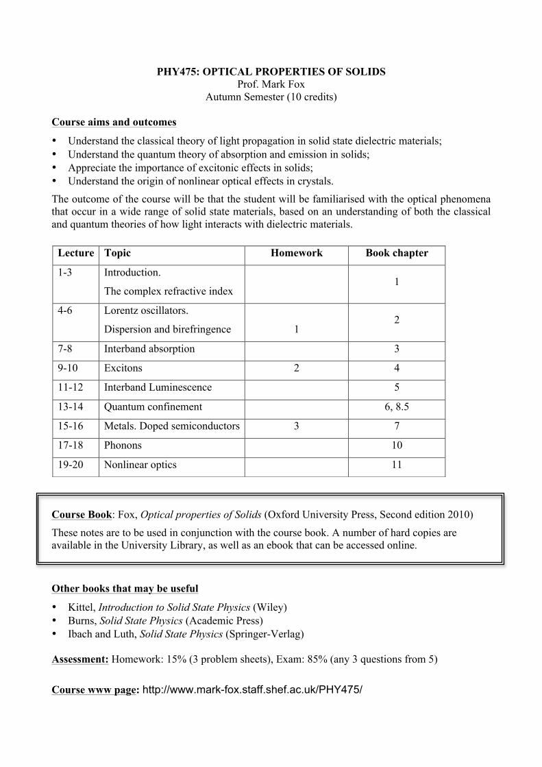
Lecture Topic Homework Book chapter
1-3 Introduction.
The complex refractive index
1
4-6 Lorentz oscillators.
Dispersion and birefringence
1 2
7-8 Interband absorption 3
9-10 Excitons 2 4
11-12 Interband Luminescence 5
13-14 Quantum confinement 6, 8.5
15-16 Metals. Doped semiconductors 3 7
17-18 Phonons 10
19-20 Nonlinear optics 11

1
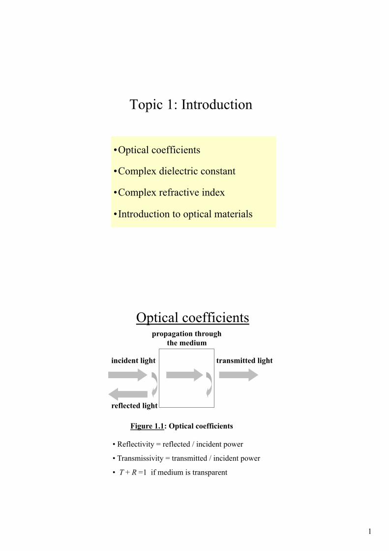
Topic 1: Introduction
• Optical coefficients
• Complex dielectric constant
• Complex refractive index
• Introduction to optical materials
Optical coefficients
Figure 1.1: Optical coefficients
incident light
reflected light
transmitted light
propagation through the medium
• Reflectivity = reflected / incident power
• Transmissivity = transmitted / incident power
• T + R =1 if medium is transparent
2
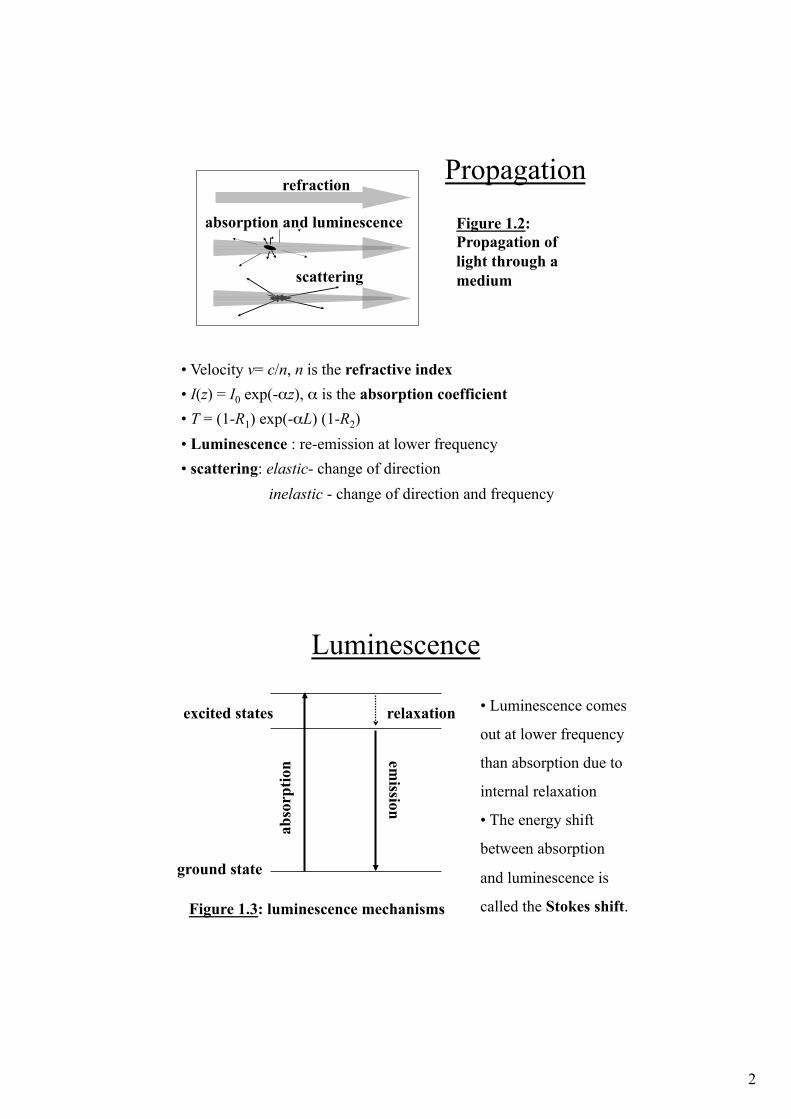
Propagation refraction
absorption and luminescence
scattering
Figure 1.2: Propagation of light through a medium
• Velocity v= c/n, n is the refractive index • I(z) = I0 exp(-αz), α is the absorption coefficient • T = (1-R1) exp(-αL) (1-R2) • Luminescence : re-emission at lower frequency • scattering: elastic- change of direction inelastic - change of direction and frequency
Luminescence
Figure 1.3: luminescence mechanisms
abso
rptio
n emission
relaxation
ground state
excited states • Luminescence comes
out at lower frequency
than absorption due to
internal relaxation
• The energy shift
between absorption
and luminescence is
called the Stokes shift.
3
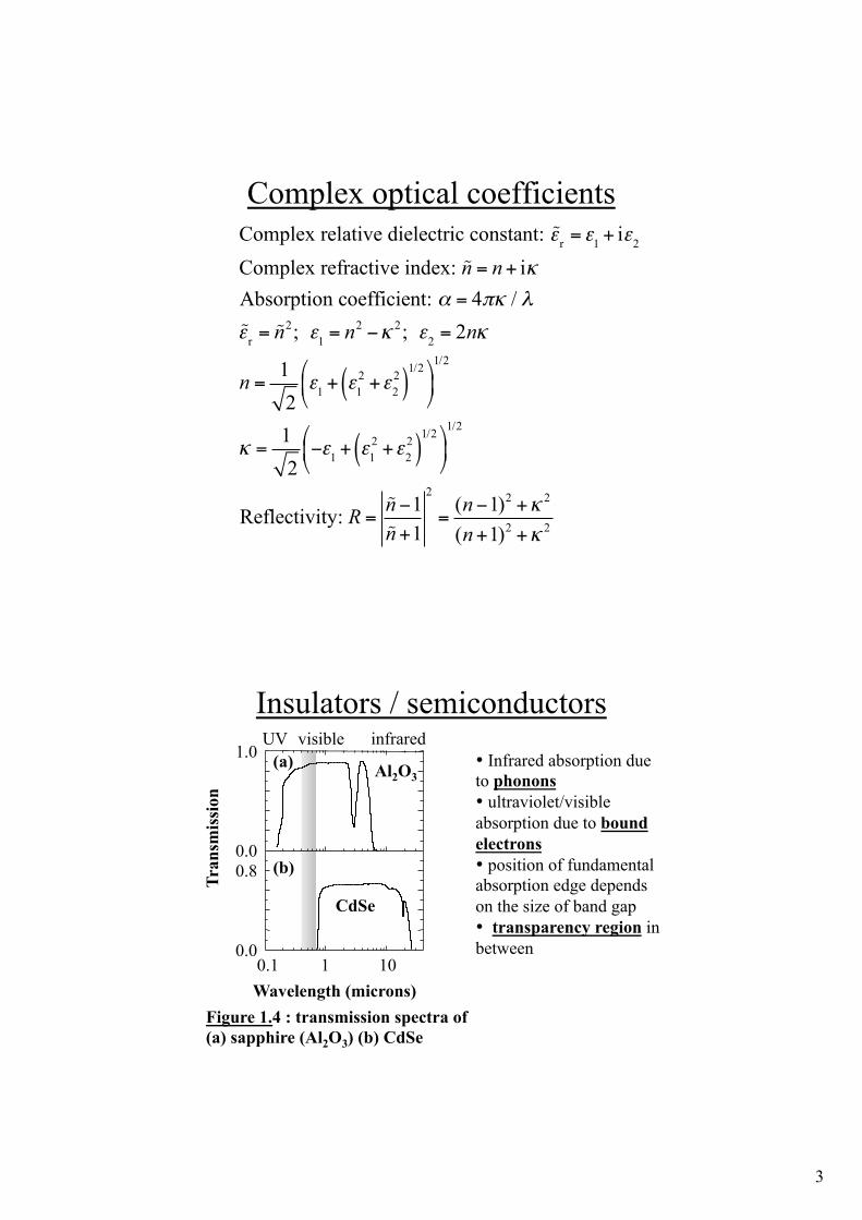
Complex optical coefficients Complex relative dielectric constant: εr = ε1 + iε2
Complex refractive index: n = n+ iκAbsorption coefficient: α = 4πκ / λεr = n
2; ε1 = n2 −κ 2; ε2 = 2nκ
n = 1
2ε1 + ε1
2 +ε22( )
1/2"#$
%&'
1/2
κ =1
2−ε1 + ε1
2 +ε22( )
1/2"#$
%&'
1/2
Reflectivity: R = n−1n+1
2
=(n−1)2 +κ 2
(n+1)2 +κ 2
Insulators / semiconductors
Figure 1.4 : transmission spectra of (a) sapphire (Al2O3) (b) CdSe
Al2O3
CdSe
Wavelength (microns)
0.0
1.0
0.1 1 10 0.0
0.8 Tran
smis
sion
infrared UV visible (a)
(b)
• Infrared absorption due to phonons • ultraviolet/visible absorption due to bound electrons • position of fundamental absorption edge depends on the size of band gap • transparency region in between

4
Metals
10 1.0 0.1 0.0 0.2 0.4 0.6 0.8 1.0
Wavelength (µm)
Ref
lect
ivity
infrared visible UV
silver
• Free electrons in the metal absorb ⇒ High reflectivity up to “plasma frequency” in the UV
Figure 1.5: Reflectivity spectrum of silver
Organic materials
Figure 1.6 : Absorption spectrum of polyfluorene
• Strong absorption in UV/visible spectral region due to
electronic transitions
• Stokes-shifted emission across the visible spectral region
300 400 500 600 700 0.0 0.2 0.4 0.6 0.8 1.0
Abs
orpt
ion
(a.u
.)
Wavelength (nm)
polyfluorene (F8)
UV/blue band UV visible
5
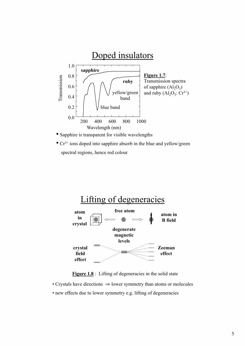
Doped insulators
200 400 600 800 1000 0.0
0.2
0.4
0.6
0.8
1.0
ruby
sapphire
Wavelength (nm)
Tran
smis
sion
yellow/green band
blue band
Figure 1.7: Transmission spectra of sapphire (Al2O3) and ruby (Al2O3: Cr3+)
• Sapphire is transparent for visible wavelengths
• Cr3+ ions doped into sapphire absorb in the blue and yellow/green
spectral regions, hence red colour
Lifting of degeneracies free atom
degenerate magnetic
levels
atom in B field
atom in
crystal
crystal field effect
Zeeman effect
Figure 1.8 : Lifting of degeneracies in the solid state
• Crystals have directions ⇒ lower symmetry than atoms or molecules
• new effects due to lower symmetry e.g. lifting of degeneracies
6
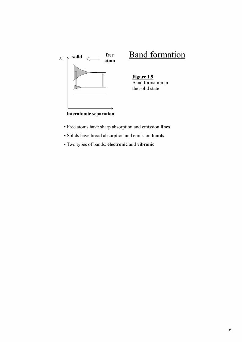
Band formation E
Interatomic separation
solid free atom
Figure 1.9: Band formation in the solid state
• Free atoms have sharp absorption and emission lines
• Solids have broad absorption and emission bands
• Two types of bands: electronic and vibronic
7
Topic 2: Dipole oscillators
• Introduction
• Lorentz oscillator model
• Kramers–Kronig relationships
• Dispersion
• Optical anisotropy & chirality
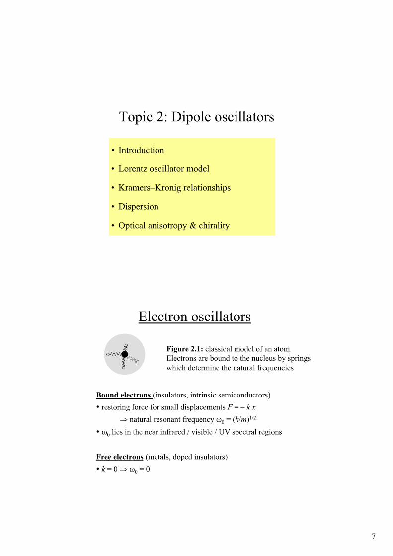
Electron oscillators
Figure 2.1: classical model of an atom. Electrons are bound to the nucleus by springs which determine the natural frequencies
Bound electrons (insulators, intrinsic semiconductors) • restoring force for small displacements F = – k x
⇒ natural resonant frequency ω0 = (k/m)1/2 • ω0 lies in the near infrared / visible / UV spectral regions Free electrons (metals, doped insulators) • k = 0 ⇒ ω0 = 0
8
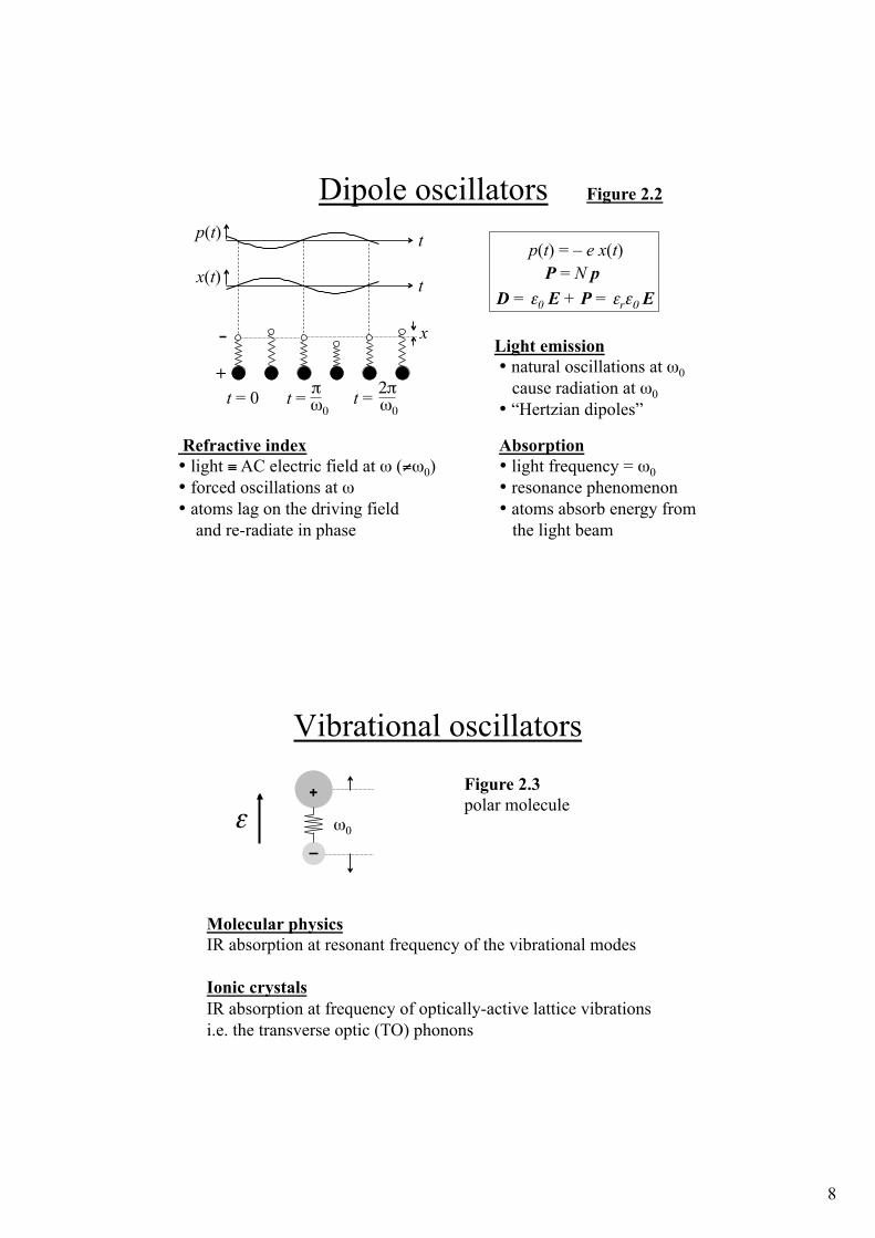
Dipole oscillators
p(t) = – e x(t) P = N p
D = ε0 E + P = εrε0 E
p(t)
t
+ t = 0 t = π
ω0 t = 2π ω0
t
x(t)
x
Refractive index • light ≡ AC electric field at ω (≠ω0) • forced oscillations at ω • atoms lag on the driving field and re-radiate in phase
Light emission • natural oscillations at ω0 cause radiation at ω0 • “Hertzian dipoles”
Absorption • light frequency = ω0 • resonance phenomenon • atoms absorb energy from the light beam
Figure 2.2
Vibrational oscillators
Figure 2.3 polar molecule
+
ε
Molecular physics IR absorption at resonant frequency of the vibrational modes Ionic crystals IR absorption at frequency of optically-active lattice vibrations i.e. the transverse optic (TO) phonons
ω0
9
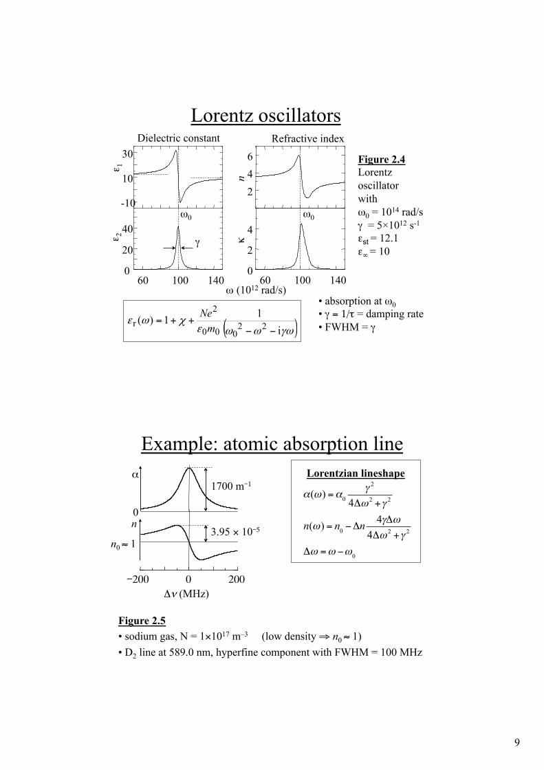
Lorentz oscillators Dielectric constant Refractive index
Figure 2.4 Lorentz oscillator with ω0 = 1014 rad/s γ = 5×10¹² s-1
εst = 12.1 ε∞ = 10
-10
10
30
ε 1
60 100 140 0
20
40
ε 2
ω (1012 rad/s)
γ
ω0
2 4 6
n
60 100 140 0
2
4 κ
ω0
( )γωωωεχωε
i11)( 22
000
2r
−−++=
mNe
• absorption at ω0 • γ = 1/τ = damping rate • FWHM = γ,
Example: atomic absorption line
Figure 2.5 • sodium gas, N = 1×10¹⁷ m–3 (low density ⇒ n0 ≈ 1) • D2 line at 589.0 nm, hyperfine component with FWHM = 100 MHz
n0 ≈ 1
�200, 0, 200,Δν (MHz)
n
α
0
1700 m�1
3.95 × 10�5
α(ω) =α0γ 2
4Δω 2 +γ 2
n(ω) = n0 −Δn4γΔω
4Δω 2 +γ 2
Δω =ω −ω0
Lorentzian lineshape
10
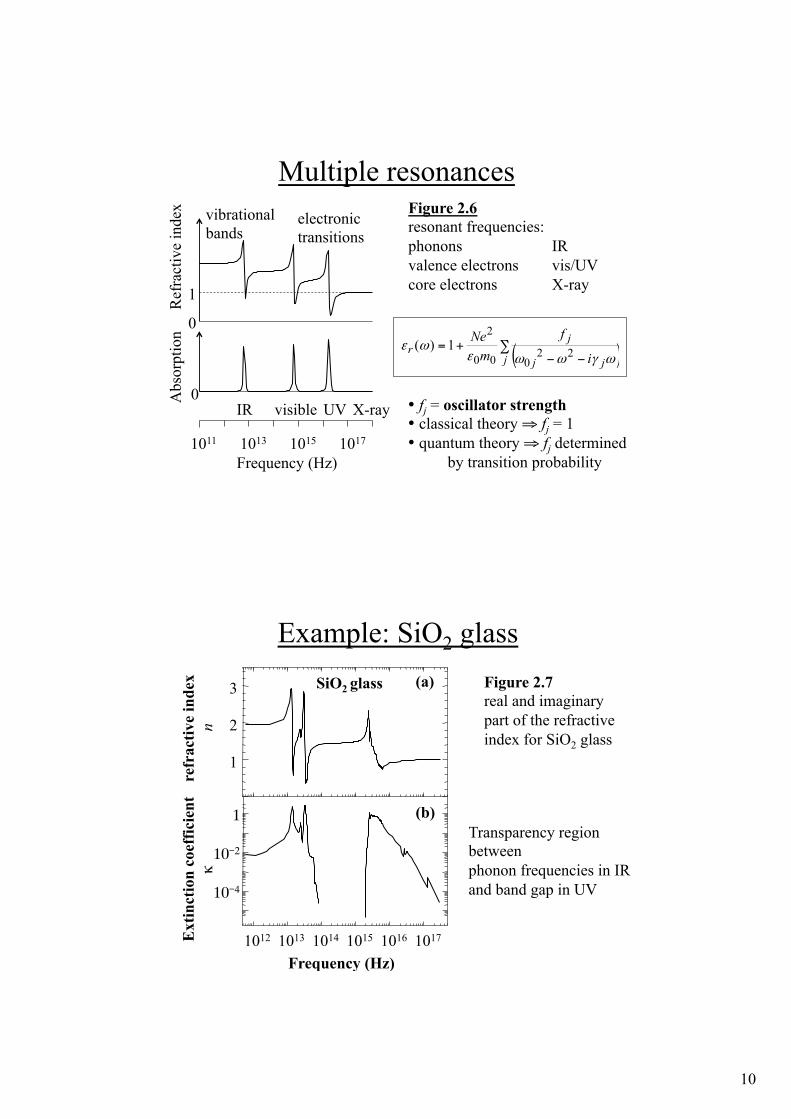
Multiple resonances Figure 2.6 resonant frequencies: phonons IR valence electrons vis/UV core electrons X-ray
0
1 Ref
ract
ive
inde
x A
bsor
ptio
n
1011 1013 1015 1017 Frequency (Hz)
0
vibrational bands
electronic transitions
IR visible UV X-ray • fj = oscillator strength • classical theory ⇒ fj = 1 • quantum theory ⇒ fj determined by transition probability
( )∑−−
+=j jj
jr
i
fmNe
ωγωωεωε 22
000
21)(
Example: SiO2 glass
1012 1013 1014 1015 1016 1017
10�4,
10�2,
1,
Ext
inct
ion
coef
ficie
nt
κ
Frequency (Hz)
(b)
1
2
3
refr
activ
e in
dex
n
(a) SiO2 glass Figure 2.7 real and imaginary part of the refractive index for SiO2 glass
Transparency region between phonon frequencies in IR and band gap in UV
11
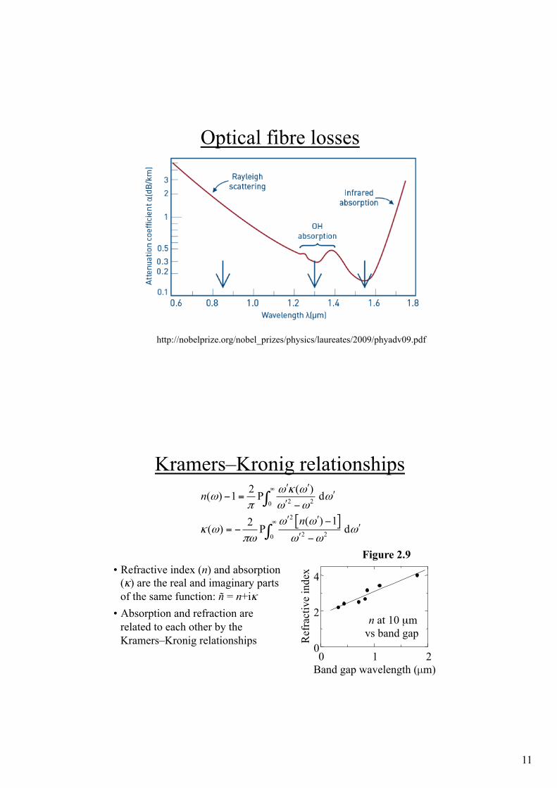
Optical fibre losses
http://nobelprize.org/nobel_prizes/physics/laureates/2009/phyadv09.pdf
Kramers–Kronig relationships
[ ]
2 20
2
2 20
2 ( )( ) 1 P d
( ) 12( ) P d
n
n
ω κ ωω ω
π ω ωω ω
κ ω ωπω ω ω
∞
∞
% %%− =
% −% % −
%= −% −
∫
∫
0 1 2 0
2
4
Ref
ract
ive
inde
x
Band gap wavelength (µm)
• Refractive index (n) and absorption (κ) are the real and imaginary parts of the same function: ñ = n+iκ
• Absorption and refraction are related to each other by the Kramers–Kronig relationships $
n at 10 µm vs band gap
Figure 2.9
12
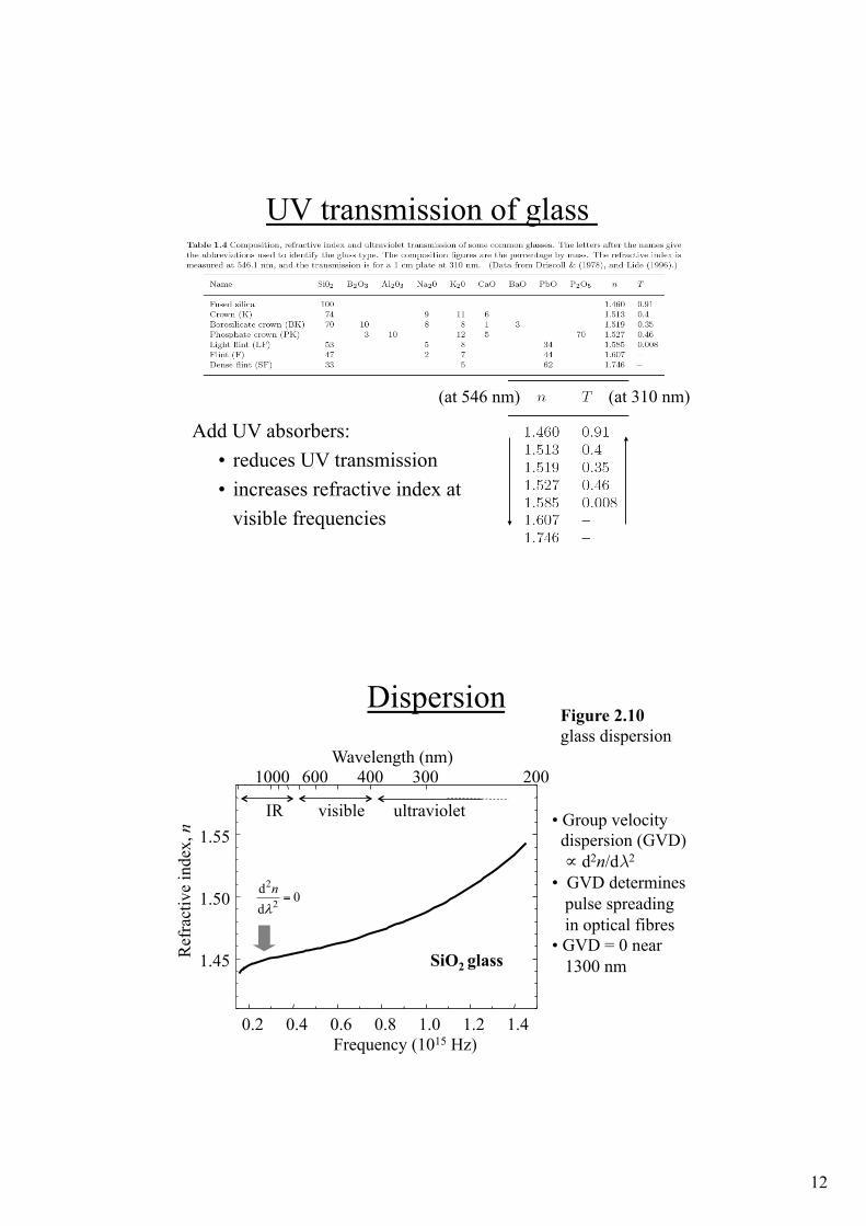
UV transmission of glass
Add UV absorbers: • reduces UV transmission • increases refractive index at
visible frequencies
(at 310 nm) (at 546 nm)
Dispersion Figure 2.10 glass dispersion
0.2 0.4 0.6 0.8 1.0 1.2 1.4
1.45
1.50
1.55
Ref
ract
ive
inde
x, n
Frequency (1015 Hz)
1000 600 400 300 200 Wavelength (nm)
SiO2 glass
2
2d 0dnλ
=
visible ultraviolet IR • Group velocity dispersion (GVD) ∝ d2n/d!2
• GVD determines pulse spreading in optical fibres • GVD = 0 near 1300 nm
13
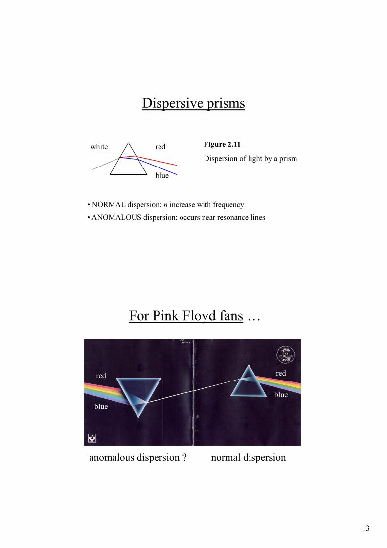
Dispersive prisms
blue
red white Figure 2.11
Dispersion of light by a prism
• NORMAL dispersion: n increase with frequency
• ANOMALOUS dispersion: occurs near resonance lines
For Pink Floyd fans …
normal dispersion anomalous dispersion ?
red red
blue blue
14
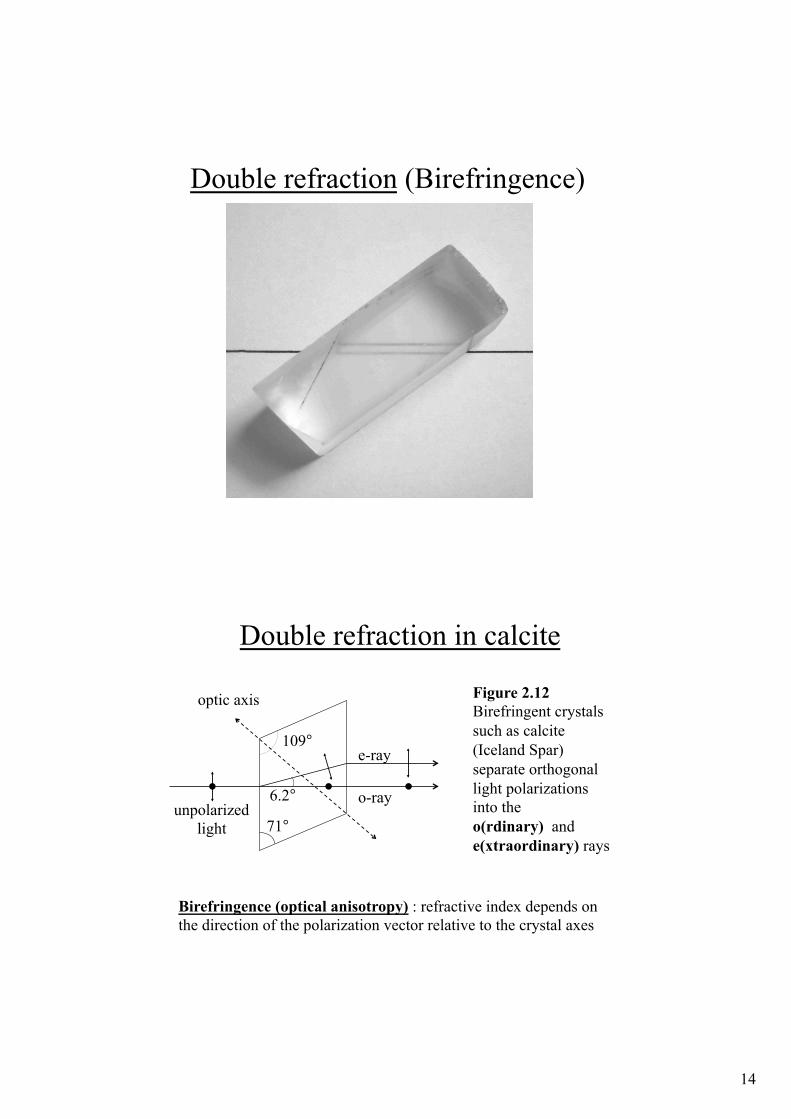
Double refraction (Birefringence)
Double refraction in calcite
Figure 2.12 Birefringent crystals such as calcite (Iceland Spar) separate orthogonal light polarizations into the o(rdinary) and e(xtraordinary) rays
109°
71°
6.2°
e-ray
o-ray unpolarized
light
optic axis
Birefringence (optical anisotropy) : refractive index depends on the direction of the polarization vector relative to the crystal axes
15
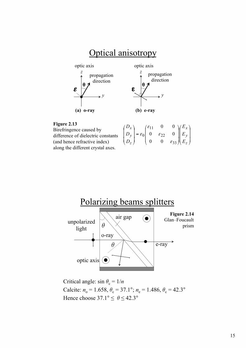
Optical anisotropy
θ
y
z optic axis
propagation direction
(b) e-ray
ε θ
y
z optic axis
propagation direction
(a) o-ray
ε
Figure 2.13 Birefringence caused by difference of dielectric constants (and hence refractive index) along the different crystal axes.
!!!
"
#
$$$
%
&
!!!
"
#
$$$
%
&=
!!!
"
#
$$$
%
&
z
y
x
z
y
x
EEE
DDD
33
22
11
000
0000
ε
ε
ε
ε
Polarizing beams splitters
e-ray o-ray
unpolarized light "
air gap
optic axis
"
Critical angle: sin "c = 1/n Calcite: no = 1.658, "c = 37.1°; ne = 1.486, "c = 42.3° Hence choose 37.1° ≤ " ≤ 42.3°
Figure 2.14 Glan–Foucault
prism

16
Wave plates
(b) (a) "
optic
axis
d
input output "
o-ray e-ray
input polarization
( )o e2 n n dπ
φλ
Δ = − Half wave plate: !# = $ Quarter wave plate: Δφ = π / 2,
Figure 2.15
Induced birefringence • Isotropic materials are non-birefringent • Induce birefringence !n with strain or electric field • Hence photo-elastic and electro-optic effects • Kerr effect (quadratic electro-optic effect) observed in
all materials, including liquids and glass: Δn = ! K E2 ; K = Kerr constant
• Hence Kerr cells (see Fig. 11.8) • Contrast with linear electro-optic effect (Pockels effect)
observed only in anisotropic crystals (See Fig 11.6)

17
Chirality
( )R Ld n nπ
θλ
= −
• Optical properties different for left or right circularly polarized light due to chirality (helicity) of molecules or crystal structure
• Circular dichroism: different absorption for left or right circular light
• Optical activity: different refractive index for left or right circular light.
• Optical activity causes rotation of linear light: Examples: dextrose, laevulose (fructose) [latin dexter, laevus]
amino acid
Magneto-optics • Induce chirality in non-chiral materials with a magnetic
field • magnetic circular dichrosim in absorbing materials • Faraday effect in transparent materials: rotation of linear
polarization by magnetic field $θ = V B d ; V = Verdet coefficient
"
d
input output
B
Figure 2.16 The Faraday effect

18
Appendix: Local field corrections Figure 2.8 local field ≠ applied field in dense medium
+ + + + + + +
- - - - - - - P
θ
ε
Lorentz correction:,εlocal = ε + P/3ε0 in cubic crystal
Clausius Mossotti relationship
321
r
r aNχεε
=+−

19
Topic 3: Interband absorption
• Interband transitions: direct and indirect
• Direct gap materials
• Optical orientation
• Indirect gap materials
• Photodetectors & solar cells
Interband absorption
Ef
Ei
!% Eg
upper band
lower band
Energy • Photon excites electron from filled valence to empty conduction band
• Fundamental absorption edge at Eg
• Process creates an electron–hole pair
Figure 3.1
20
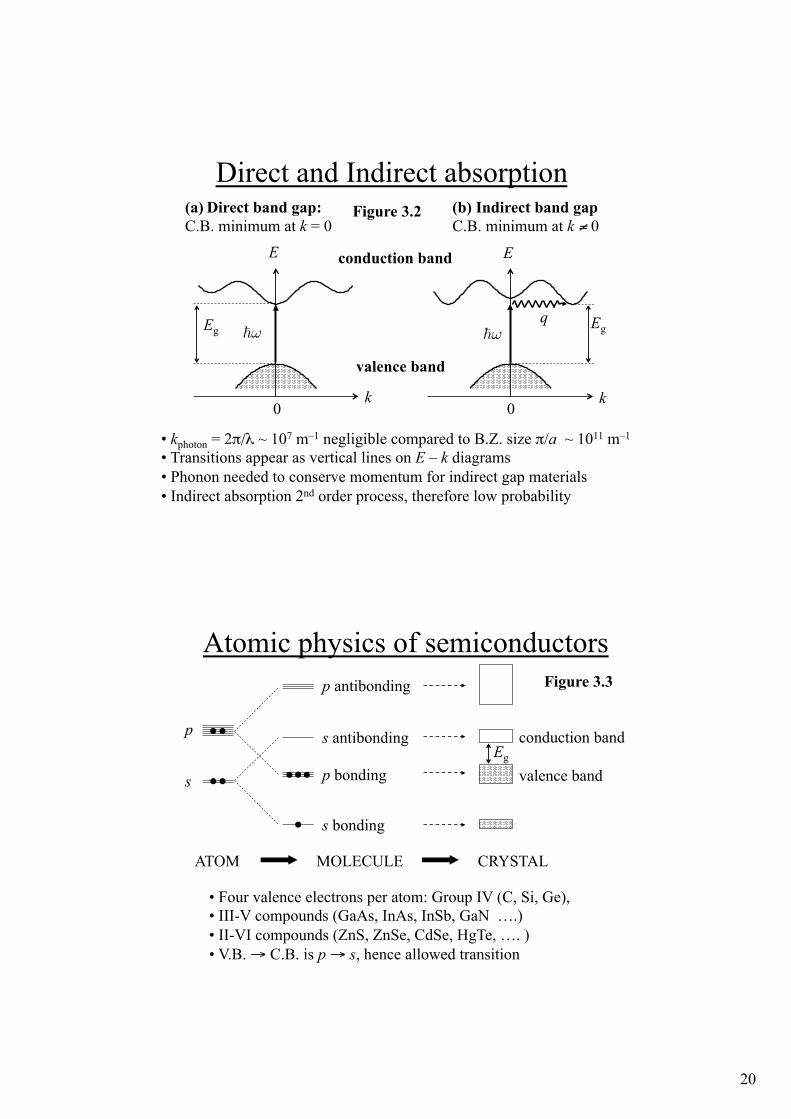
Direct and Indirect absorption
q
valence band
conduction band
(a) Direct band gap: C.B. minimum at k = 0
(b) Indirect band gap C.B. minimum at k ≠ 0
k
E
k
E
0 0
Eg Eg
• kphoton = 2π/λ ~ 107 m–1 negligible compared to B.Z. size π/a ~ 1011 m–1 • Transitions appear as vertical lines on E – k diagrams • Phonon needed to conserve momentum for indirect gap materials • Indirect absorption 2nd order process, therefore low probability
Figure 3.2
!% !%
Atomic physics of semiconductors
s
p
s bonding
s antibonding
p bonding
p antibonding
ATOM MOLECULE CRYSTAL
Eg valence band
conduction band
Figure 3.3
• Four valence electrons per atom: Group IV (C, Si, Ge), • III-V compounds (GaAs, InAs, InSb, GaN ….) • II-VI compounds (ZnS, ZnSe, CdSe, HgTe, …. ) • V.B. → C.B. is p → s, hence allowed transition
21
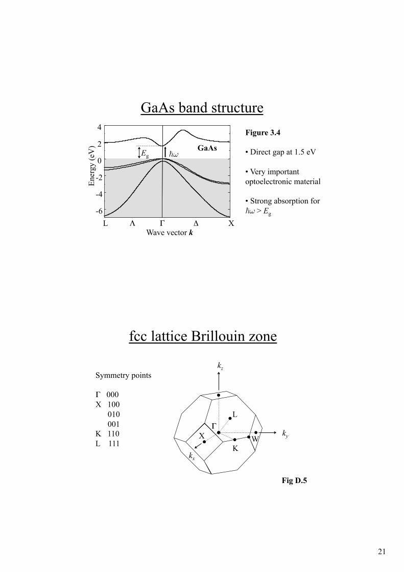
GaAs band structure Figure 3.4 • Direct gap at 1.5 eV • Very important optoelectronic material
• Strong absorption for !% > Eg -6
-4
-2
0
2
4
Ener
gy (e
V)
Γ X L
Eg !% GaAs
Wave vector k Λ, Δ,
fcc lattice Brillouin zone
Γ,X
L
K W
kz
kx
ky
Symmetry points Γ 000 X 100 010 001 K 110 L 111
Fig D.5
22
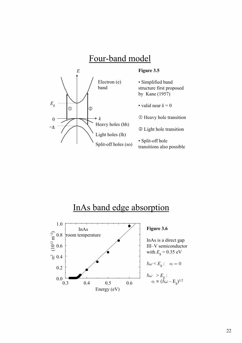
Four-band model
k
E
Electron (e) band
Heavy holes (hh)
Light holes (lh)
Split-off holes (so)
Eg
0 �Δ
! "
Figure 3.5 • Simplified band structure first proposed by Kane (1957)
• valid near k = 0 ! Heavy hole transition
" Light hole transition
• Split-off hole transitions also possible
InAs band edge absorption
Figure 3.6 InAs is a direct gap III–V semiconductor with Eg = 0.35 eV !% < Eg : " = 0 !% > Eg : " ∝ (!% – Eg)1/2 0.3 0.4 0.5 0.6
0.0
0.2
0.4
0.6
0.8
1.0
Energy (eV)
α2
(1012
m�2 )
InAs room temperature
23
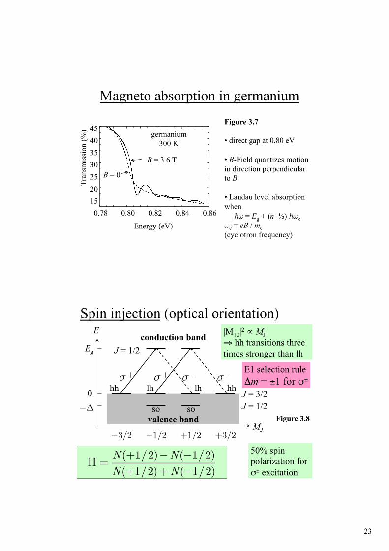
Magneto absorption in germanium
Figure 3.7 • direct gap at 0.80 eV • B-Field quantizes motion in direction perpendicular to B • Landau level absorption when !% = Eg + (n+½) !%c
%c = eB / me (cyclotron frequency)
0.78 0.80 0.82 0.84 0.86 15 20 25 30 35 40 45
Energy (eV)
Tran
smis
sion
(%) germanium
300 K
B = 3.6 T
B = 0
Spin injection (optical orientation) E
MJ
J = 3/2 J = 1/2
J = 1/2
#1/2 #3/2 +3/2 +1/2
valence band
conduction band
#! 0
Eg
& + & + & # & #
hh hh lh lh
so so Figure 3.8
|M12|2 ∝ MJ ⇒ hh transitions three times stronger than lh
( 1/2) ( 1/2)( 1/2) ( 1/2)N NN N+ ! !" =+ + !
50% spin polarization for σ± excitation
E1 selection rule Δm = ±1 for σ±
24
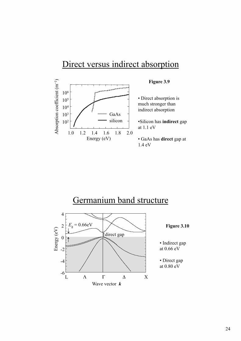
Direct versus indirect absorption
1.0 1.2 1.4 1.6 1.8 2.0
102 103 104 105 106
Energy (eV)
Abs
orpt
ion
coef
ficie
nt (m
�1 )
GaAs silicon
Figure 3.9
• Direct absorption is much stronger than indirect absorption
• Silicon has indirect gap at 1.1 eV
• GaAs has direct gap at 1.4 eV
Germanium band structure
Figure 3.10
-6
-4
-2
0
2
4
Ener
gy (e
V)
Wave vector k
Eg = 0.66eV
direct gap
L Γ,Λ, Δ, X
• Indirect gap at 0.66 eV • Direct gap at 0.80 eV
25
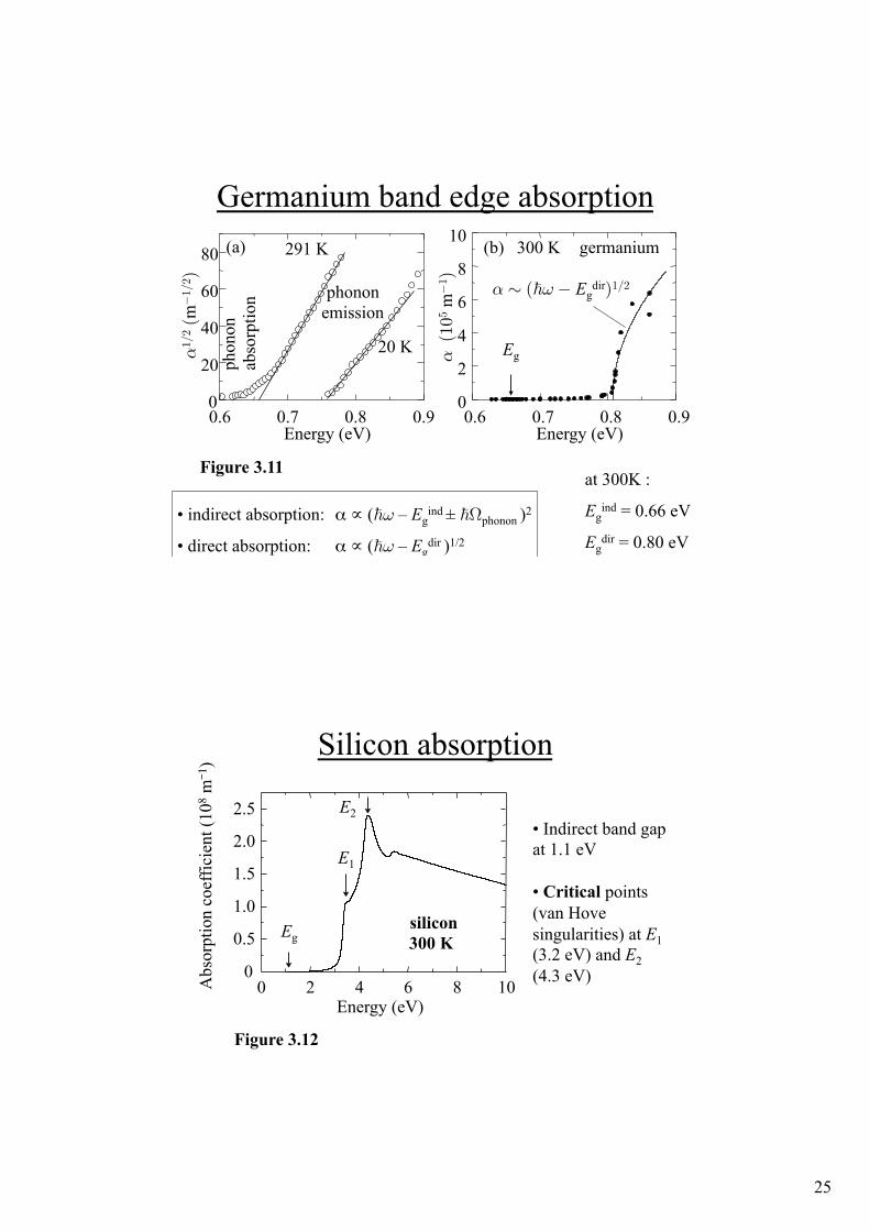
Germanium band edge absorption
Figure 3.11
• indirect absorption: α ∝ (!% – Egind ± !$phonon )2
• direct absorption: α ∝ (!% – Egdir )1/2
at 300K :
Egind = 0.66 eV
Egdir = 0.80 eV
0.6 0.7 0.8 0.9 0
20
40
60
80
'1/
2 (m#
1/2 )
Energy (eV)
phon
on
abso
rptio
n 291 K
20 K
phonon emission
(a) (b)
0.6 0.7 0.8 0.9 0
2
4
6
8
10
' (1
05 m#
1 )
Energy (eV)
' % (!% # Egdir)1/2
Eg
300 K germanium
Silicon absorption
0 2 4 6 8 10 0
0.5
1.0
1.5
2.0
2.5
Energy (eV)
Abs
orpt
ion
coef
ficie
nt (1
08 m�1 )
silicon 300 K
Eg
E1
E2
Figure 3.12
• Indirect band gap at 1.1 eV • Critical points (van Hove singularities) at E1 (3.2 eV) and E2 (4.3 eV)
26
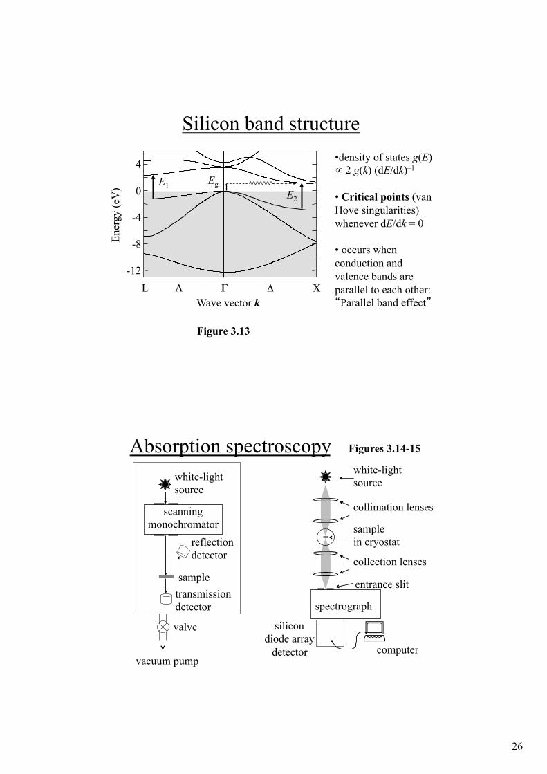
Silicon band structure
Figure 3.13
-12
-8
-4
0
4
Wave vector k
Ener
gy (e
V)
Γ, X L Λ, Δ,
E1 E2
Eg
• density of states g(E) ∝ 2 g(k) (dE/dk)–1
• Critical points (van Hove singularities) whenever dE/dk = 0 • occurs when conduction and valence bands are parallel to each other: �Parallel band effect�
Absorption spectroscopy Figures 3.14-15
sample
white-light source
scanning monochromator
transmission detector
reflection detector
vacuum pump
valve
sample in cryostat
collection lenses
spectrograph
entrance slit
computer #
collimation lenses
white-light source
silicon diode array
detector
27
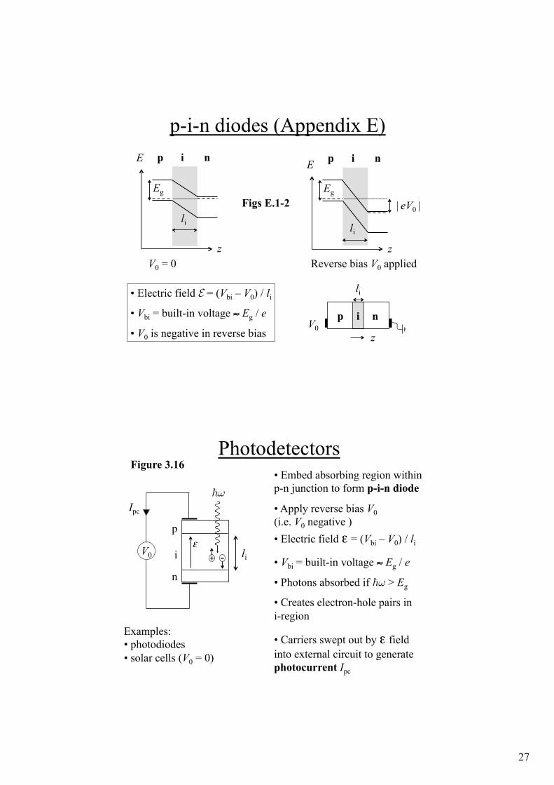
p-i-n diodes (Appendix E) p i n
li
Eg
V0 = 0 z
E
Reverse bias V0 applied
p i n
li
Eg | eV0
|
z
E
i
li
V0 z
p n
• Electric field E = (Vbi – V0) / li
• Vbi = built-in voltage ≈ Eg / e
• V0 is negative in reverse bias
Figs E.1-2
Photodetectors Figure 3.16
• Embed absorbing region within p-n junction to form p-i-n diode
• Apply reverse bias V0 (i.e. V0 negative ) • Electric field ε = (Vbi – V0) / li
• Vbi = built-in voltage ≈ Eg / e
• Photons absorbed if !% > Eg
• Creates electron-hole pairs in i-region
• Carriers swept out by ε field into external circuit to generate photocurrent Ipc
V0
Ipc
p
i
n
ε + -
!%
li
Examples: • photodiodes • solar cells (V0 = 0)
28
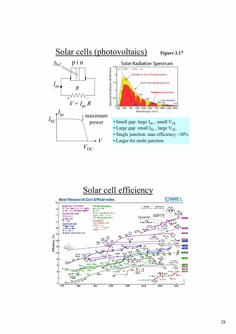
Solar cells (photovoltaics) Figure 3.17
V = Ipc R
Ipc
p i n !%
+ –
R
ISC
VOC
V
maximum power
Ipc
• Small gap: large ISC , small VOC • Large gap: small ISC , large VOC • Single junction: max efficiency ~30% • Larger for multi junction
Solar cell efficiency

29
Topic 4: Excitons
• Introduction
• Wannier excitons
• Excitonic nonlinearities
• Frenkel excitons
Excitons Figure 4.1
Free (Wannier) radius >> a small binding energy moves freely through crystal
Tightly-bound (Frenkel) radius ~ a large binding energy localized on one lattice site
e
h
h
e
a
30
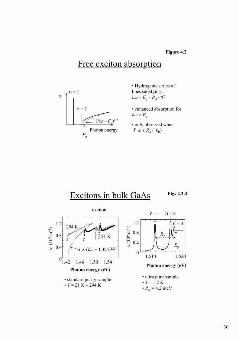
Free exciton absorption Figure 4.2
Eg
α,
Photon energy
n = 1
n = 2
(!% – Eg)1/2
• Hydrogenic series of lines satisfying : !% = Eg – RX / n2 • enhanced absorption for !% > Eg
• only observed when T ≤ ( RX / kB)
Excitons in bulk GaAs Figs 4.3-4
α (1
06 m�1 )
0.4
0.8
1.2
Photon energy (eV)
1.514 1.520 0
Eg
n = 1 n = 2
n = 3
α ∝ (!% � 1.425)1/2,
1.42 1.46 1.50 1.54 0
0.4
0.8
1.2
α (
106 m
�1 )
Photon energy (eV)
exciton,
21 K
294 K
• standard purity sample • T = 21 K – 294 K
• ultra pure sample • T = 1.2 K • RX = 4.2 meV
RX
31
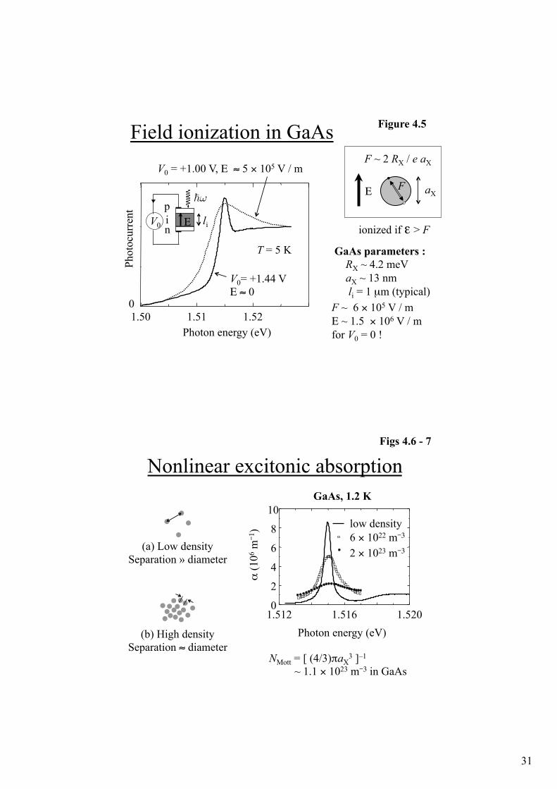
Field ionization in GaAs Figure 4.5
1.50 1.51 1.52 Photon energy (eV)
Phot
ocur
rent
T = 5 K
V0= +1.44 V$Ε ≈ 0
V0 = +1.00 V, Ε ≈ 5 × 10⁵ V / m
0
GaAs parameters : RX ~ 4.2 meV aX ~ 13 nm li = 1 µm (typical) F ~ 6 × 10⁵ V / m Ε ~ 1.5 × 10⁶ V / m for V0 = 0 !
F aX
F ~ 2 RX / e aX
ionized if ε > F
Ε,!% p i n
V0 li Ε
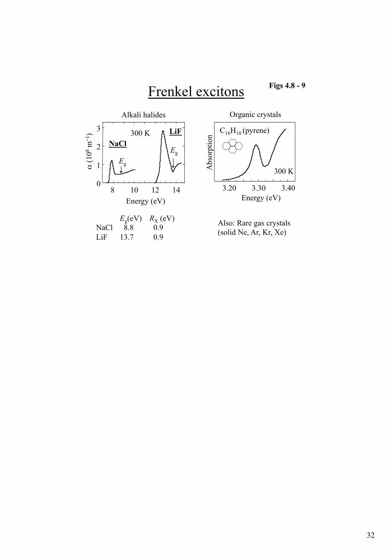
Nonlinear excitonic absorption Figs 4.6 - 7
(a) Low density Separation » diameter
(b) High density Separation ≈ diameter
1.512 1.516 1.520 0
2
4
6
8
10
Photon energy (eV)
α (1
06 m�1 )
low density 6 × 10²² m�3
2 × 10²³ m�3
GaAs, 1.2 K
NMott = [ (4/3)πaX3 ]–1
~ 1.1 × 10²³ m�3 in GaAs
32
Frenkel excitons
8 10 12 14 0
1
2
3
α (1
08 m�1 )
Energy (eV)
Eg(eV) RX (eV) NaCl 8.8 0.9 LiF 13.7 0.9
Eg Eg
LiF NaCl
300 K
Figs 4.8 - 9
300 K
3.20 3.30 3.40
Abs
orpt
ion
C16H10 (pyrene)
Energy (eV)
Alkali halides Organic crystals
Also: Rare gas crystals (solid Ne, Ar, Kr, Xe)
33
Topic 5: Luminescence
• Introduction
• Photoluminescence
• Electroluminescence
• LEDs and lasers
• Cathodoluminescence
Luminescence
• Luminescence spontaneous emission in solids
• Fluorescence fast luminescence electric-dipole allowed, τR ~ ns
• Phosphorescence slow luminescence electric-dipole forbidden, τR ~ µs – ms
• Electroluminescence electrical excitation • Photoluminescence optical excitation • Cathodoluminescence cathode ray (e–beam) excitation
34
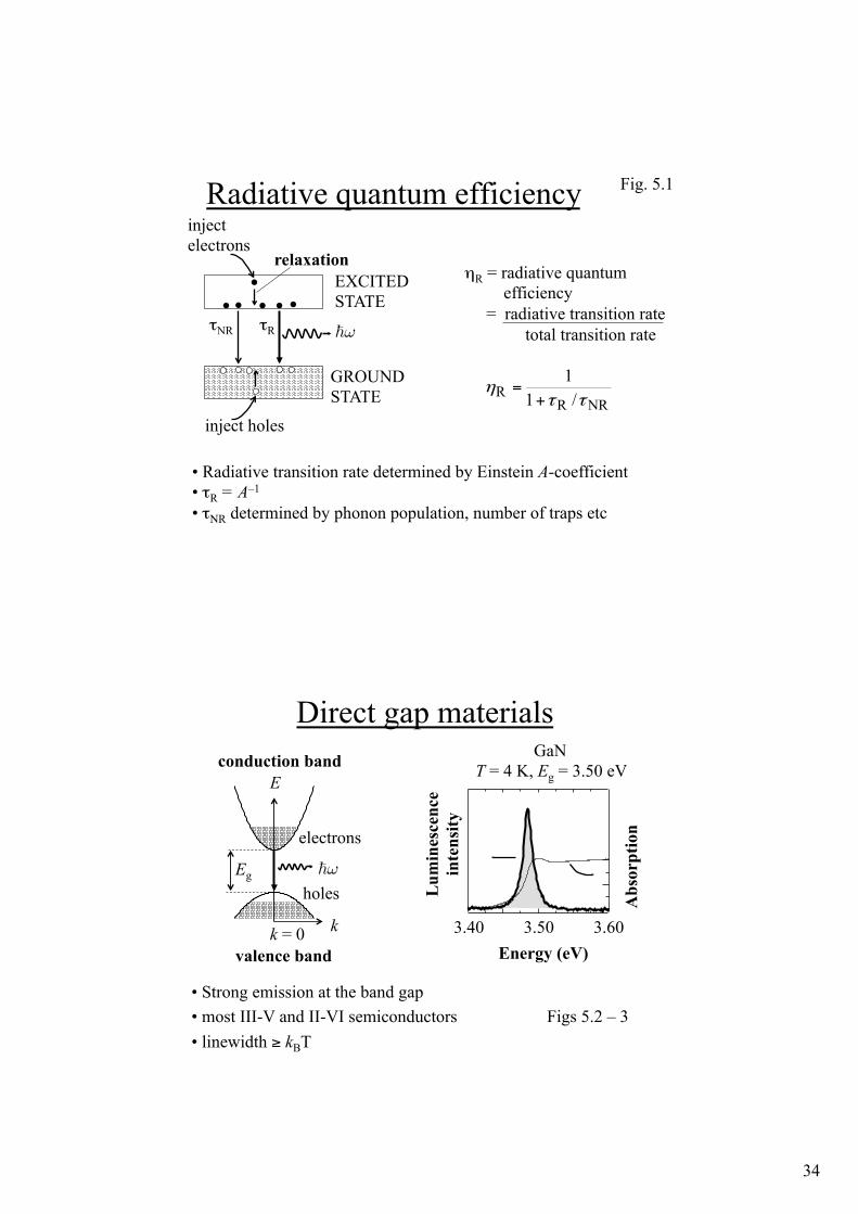
Radiative quantum efficiency
!%
inject electrons
inject holes
relaxation
τNR τR
GROUND STATE
EXCITED STATE
Fig. 5.1
• Radiative transition rate determined by Einstein A-coefficient • τR = A–1 • τΝR determined by phonon population, number of traps etc
NRRR /1
1ττ
η+
=
ηR = radiative quantum efficiency = radiative transition rate total transition rate
Direct gap materials
!%
electrons
holes
conduction band
valence band
Eg
E
k k = 0
GaN T = 4 K, Eg = 3.50 eV
3.40 3.50 3.60
Lum
ines
cenc
e
inte
nsity
Energy (eV)
Abs
orpt
ion
• Strong emission at the band gap • most III-V and II-VI semiconductors • linewidth ≥ kBT
Figs 5.2 – 3
35
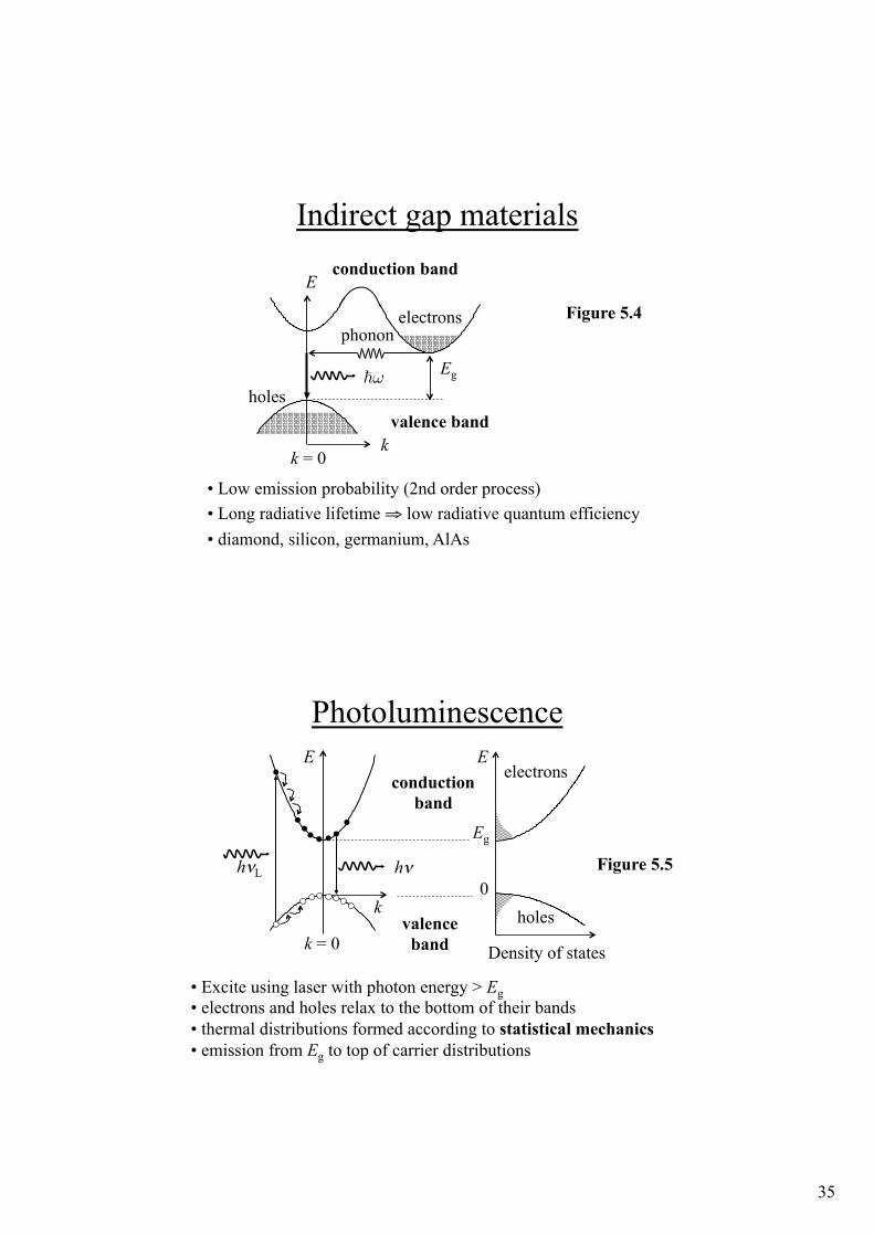
Indirect gap materials
Figure 5.4
!%
electrons
holes
conduction band
valence band
Eg
E
k
phonon
k = 0
• Low emission probability (2nd order process) • Long radiative lifetime ⇒ low radiative quantum efficiency • diamond, silicon, germanium, AlAs
Photoluminescence
hν
electrons
holes
conduction band
valence band
Eg
E
k
k = 0
0 hνL
Density of states
E
• Excite using laser with photon energy > Eg • electrons and holes relax to the bottom of their bands • thermal distributions formed according to statistical mechanics • emission from Eg to top of carrier distributions
Figure 5.5
36
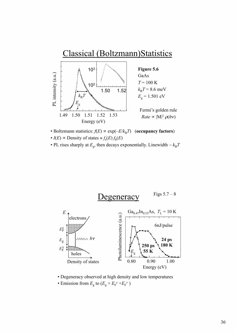
Classical (Boltzmann)Statistics
Figure 5.6 GaAs T = 100 K kBT = 8.6 meV Eg = 1.501 eV
1.49 1.50 1.51 1.52 1.53
1.50 1.52 102
103
PL in
tens
ity (a
.u.)
Energy (eV)
Eg kBT
• Boltzmann statistics: f(E) ∝ exp(–E/kBT) (occupancy factors) • I(E) ∝ Density of states × fe(E) fh(E) • PL rises sharply at Eg, then decays exponentially. Linewidth ~ kBT
Fermi’s golden rule Rate ∝ |M|2 ρ(hν)
Degeneracy
electrons
holes
Density of states
E
cFE
vFE
gE hν
0.80 0.90 1.00 Phot
olum
ines
cenc
e (a
.u.) Ga0.47In0.53As, TL = 10 K
24 ps 180 K 250 ps
55 K
Energy (eV)
Eg
6nJ/pulse
Figs 5.7 – 8
• Degeneracy observed at high density and low temperatures • Emission from Eg to (Eg + EF
c +EFv )
37
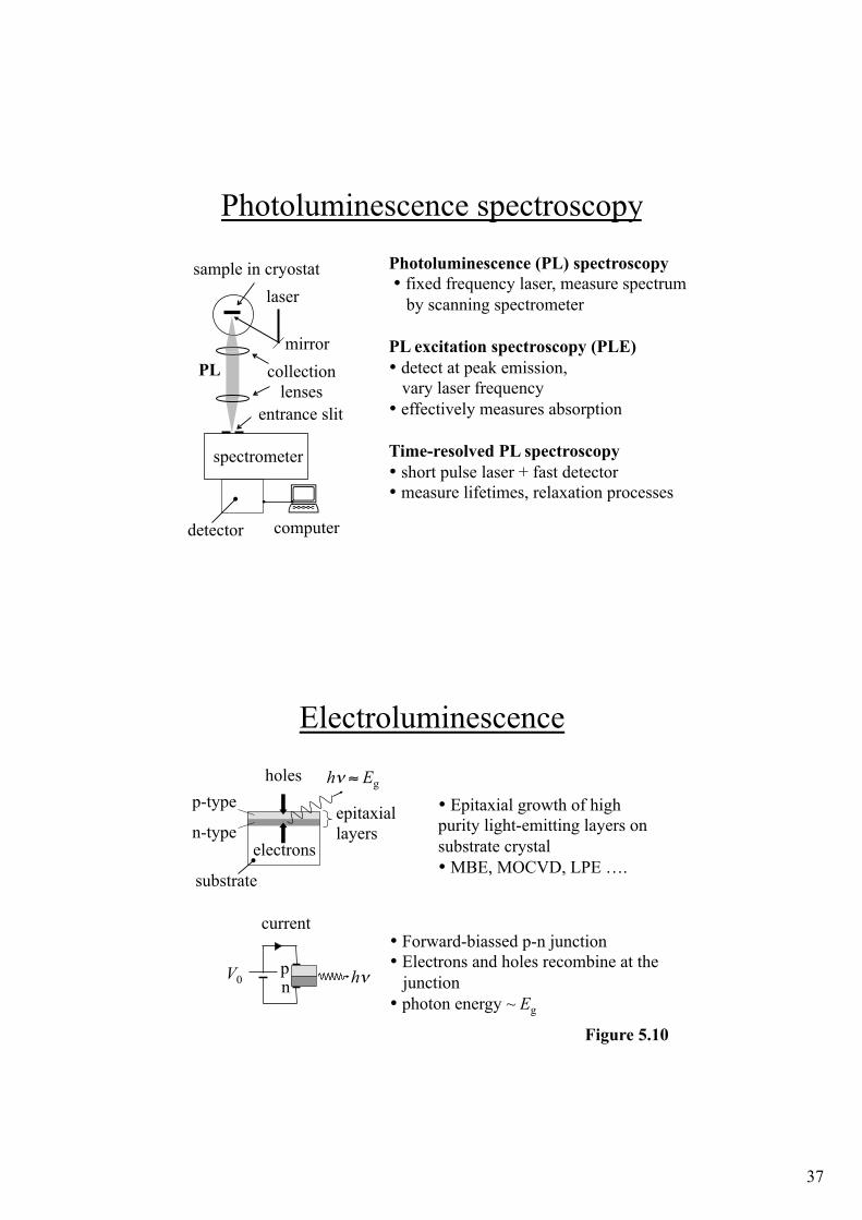
Photoluminescence spectroscopy
sample in cryostat
collection lenses
laser
PL
entrance slit
computer detector
spectrometer
#
mirror
Photoluminescence (PL) spectroscopy • fixed frequency laser, measure spectrum by scanning spectrometer PL excitation spectroscopy (PLE) • detect at peak emission, vary laser frequency • effectively measures absorption Time-resolved PL spectroscopy • short pulse laser + fast detector • measure lifetimes, relaxation processes
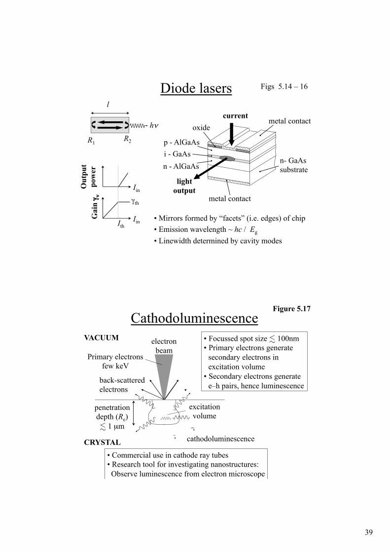
Electroluminescence
p n
hν ≈ Eg
current
V0
p-type
n-type
substrate
epitaxial layers
holes
electrons
hν
• Forward-biassed p-n junction • Electrons and holes recombine at the junction • photon energy ~ Eg
• Epitaxial growth of high purity light-emitting layers on substrate crystal • MBE, MOCVD, LPE ….
Figure 5.10
38
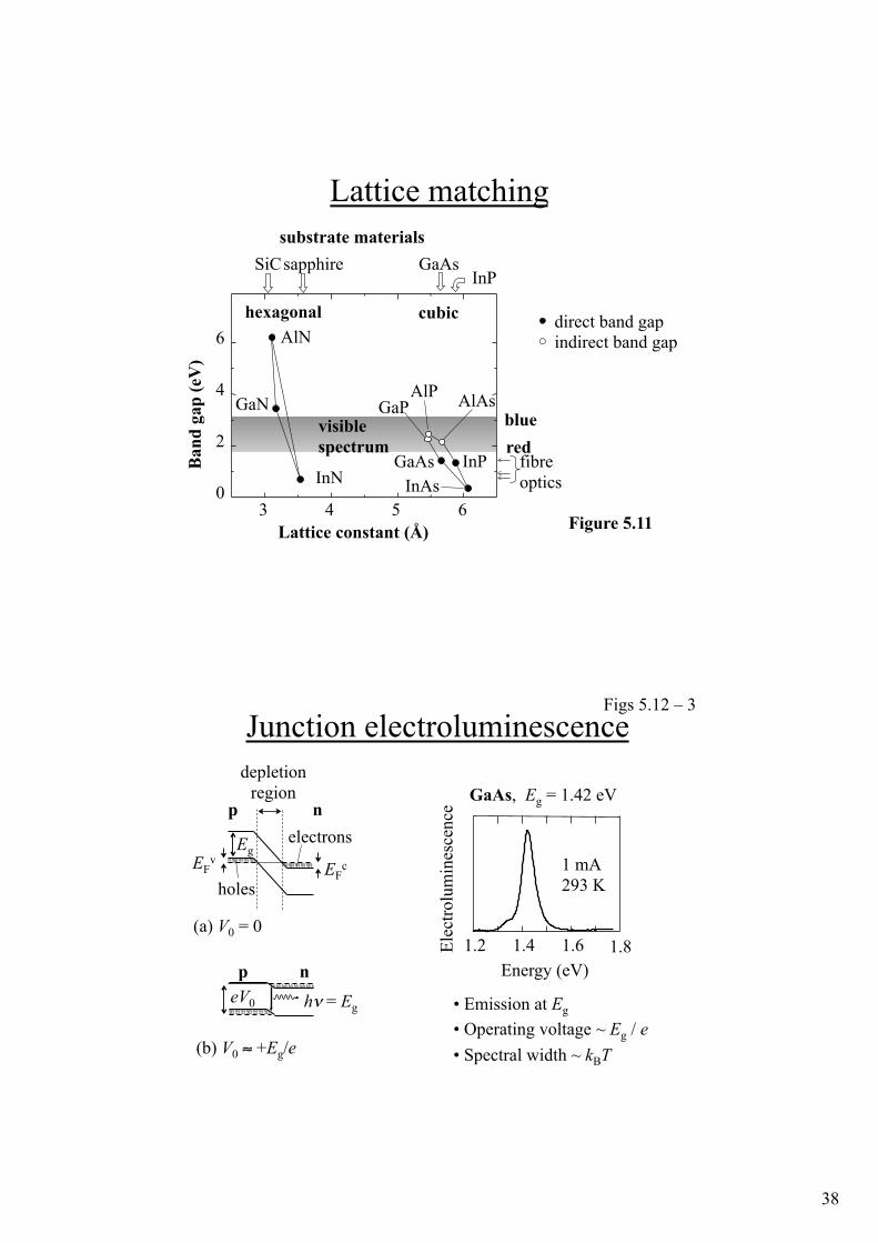
Lattice matching
3 4 5 6 0
2
4
6
Ban
d ga
p (e
V)
Lattice constant (Å)
AlN
GaN
InN InAs
AlAs
InP
AlP GaP
SiC GaAs
GaAs
InP
blue red
substrate materials
direct band gap indirect band gap
sapphire
visible spectrum
fibre optics
hexagonal cubic
Figure 5.11
1.2 1.4 1.6 Energy (eV)
1 mA 293 K
Junction electroluminescence
(a) V0 = 0
p n
Eg
holes
electrons
depletion region
(b) V0 ≈ +Eg/e
p n
hν = Eg eV0
EFc EF
v
1.8
GaAs, Eg = 1.42 eV
Elec
trolu
min
esce
nce
• Emission at Eg
• Operating voltage ~ Eg / e • Spectral width ~ kBT
Figs 5.12 – 3
39
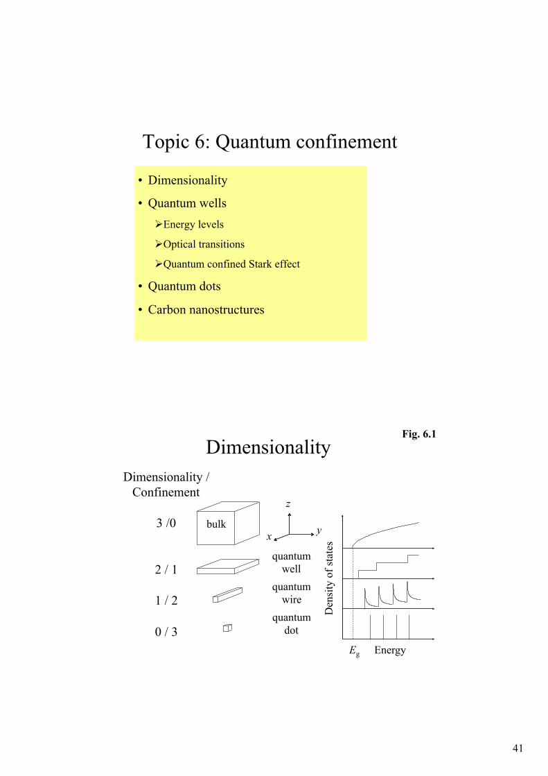
Diode lasers
hν
R1 R2
l G
ain γ ν
,
Iin Ith
γth
Out
put
pow
er ,
Iin
p - AlGaAs i - GaAs n - AlGaAs
light output
metal contact oxide
current
metal contact
n- GaAs substrate
• Mirrors formed by “facets” (i.e. edges) of chip • Emission wavelength ~ hc / Eg
• Linewidth determined by cavity modes
Figs 5.14 – 16
Cathodoluminescence
back-scattered electrons
excitation volume
penetration depth (Re) ! 1 µm
electron beam
VACUUM
CRYSTAL cathodoluminescence
• Commercial use in cathode ray tubes • Research tool for investigating nanostructures: Observe luminescence from electron microscope
• Focussed spot size ! 100nm • Primary electrons generate
secondary electrons in excitation volume
• Secondary electrons generate e–h pairs, hence luminescence
Primary electrons few keV
Figure 5.17

40
41
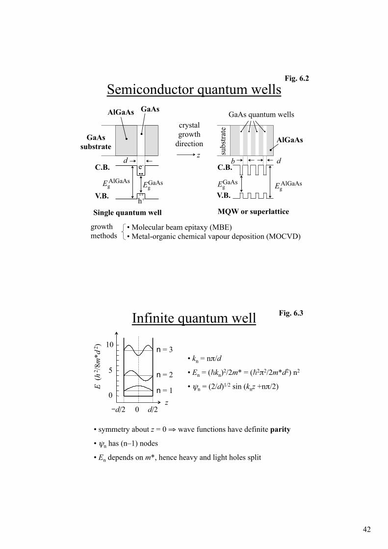
Topic 6: Quantum confinement
• Dimensionality
• Quantum wells $ Energy levels
$ Optical transitions
$ Quantum confined Stark effect
• Quantum dots
• Carbon nanostructures
Dimensionality
z
x y bulk
quantum well
quantum wire
quantum dot
Energy
Den
sity
of s
tate
s
Eg
Dimensionality / Confinement
3 /0
2 / 1
1 / 2
0 / 3
Fig. 6.1
42
Semiconductor quantum wells
d
GaAs quantum wells
C.B.
V.B.
b
AlGaAs
subs
trate
d
AlGaAs
z e-
h+
crystal growth
direction
C.B.
V.B. Eg GaAs Eg AlGaAs
GaAs substrate
GaAs
Single quantum well MQW or superlattice
Fig. 6.2
Eg GaAs Eg AlGaAs
• Molecular beam epitaxy (MBE) • Metal-organic chemical vapour deposition (MOCVD)
growth methods
Infinite quantum well Fig. 6.3
0
5
10
0 d/2 �d/2
n = 1
n = 2
n = 3
z
E (h
2/8
m*d
2)
• kn = nπ/d
• En = (!kn)2/2m* = (!2π2/2m*d2) n2
• ψn = (2/d)1/2 sin (knz +nπ/2)
• symmetry about z = 0 ⇒ wave functions have definite parity
• ψn has (n–1) nodes
• En depends on m*, hence heavy and light holes split
43
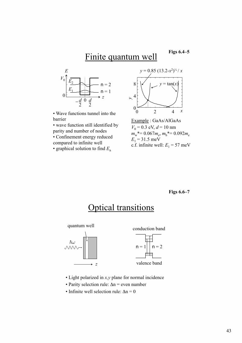
Finite quantum well Figs 6.4–5
0
4
8
0 2 4 x
y
y = tan(x)
y = 0.85 (13.2-x2)½ / x V0 E2
E1 0
E
n = 1 n = 2
d 2
z 0 d
2 –
• Wave functions tunnel into the barrier • wave function still identified by parity and number of nodes • Confinement energy reduced compared to infinite well • graphical solution to find En
Example : GaAs/AlGaAs V0 = 0.3 eV, d = 10 nm mw*= 0.067me, mb*= 0.092me E1 = 31.5 meV c.f. infinite well: E1 = 57 meV
Optical transitions
Figs 6.6–7
quantum well
!%
z
n = 2 n = 1
conduction band
valence band
• Light polarized in x,y plane for normal incidence • Parity selection rule: Δn = even number • Infinite well selection rule: Δn = 0
44
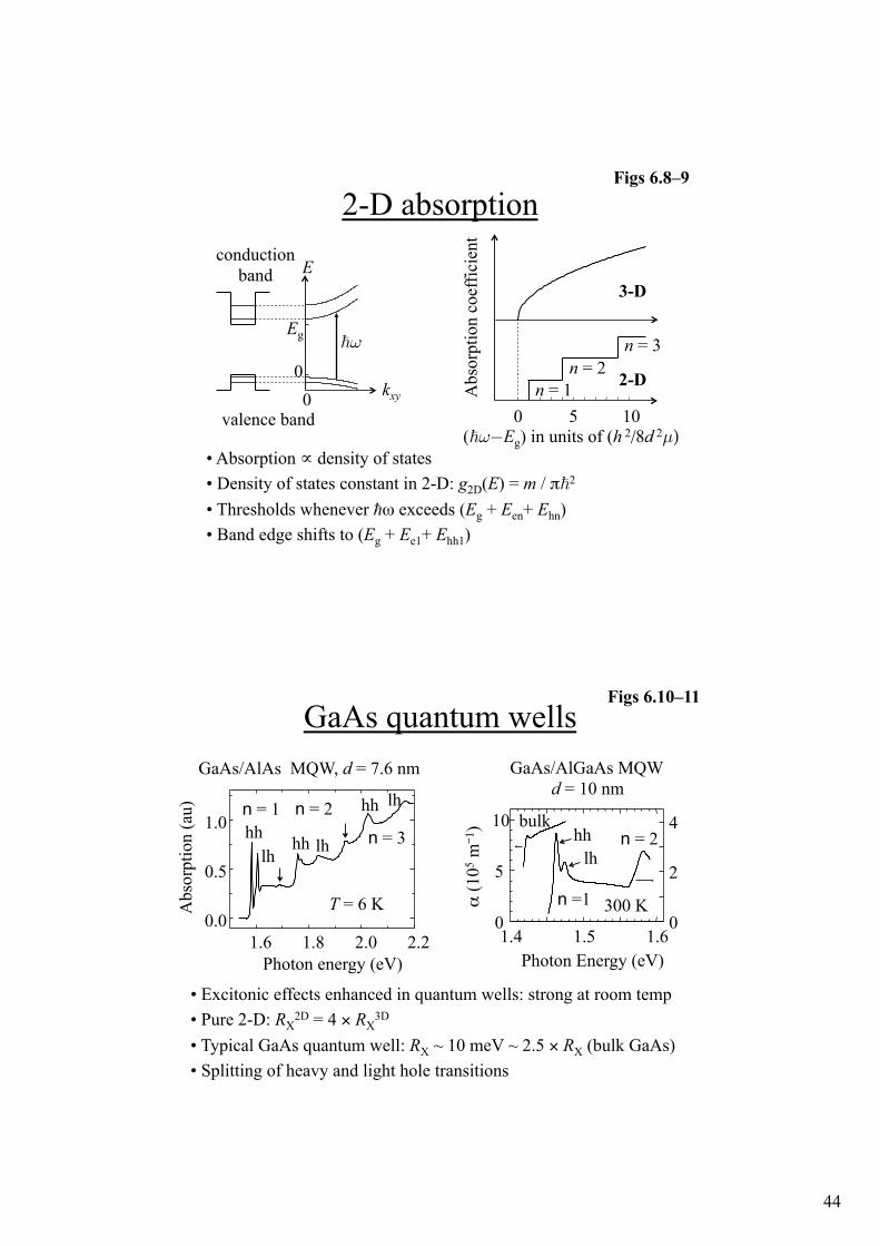
2-D absorption
0
Eg
E
!%
kxy
conduction band
valence band 0
Figs 6.8–9
• Absorption ∝ density of states • Density of states constant in 2-D: g2D(E) = m / π!2 • Thresholds whenever !ω exceeds (Eg + Een+ Ehn) • Band edge shifts to (Eg + Ee1+ Ehh1)
0 5 10 (!%#Eg) in units of (h 2/8d 2µ)
Abs
orpt
ion
coef
ficie
nt
3-D
2-D n = 1 n = 2
n = 3
GaAs quantum wells GaAs/AlGaAs MQW
d = 10 nm
1.4 1.5 1.6 0
5
10
Photon Energy (eV)
α (1
05 m�1 )
0
2
4 bulk
n =1
n = 2 hh lh
300 K
Figs 6.10–11
GaAs/AlAs MQW, d = 7.6 nm
Photon energy (eV) 1.6 1.8 2.0 2.2
Abs
orpt
ion
(au)
0.0
0.5
1.0 hh lh
hh lh
n = 1 n = 2 n = 3
hh lh
T = 6 K
• Excitonic effects enhanced in quantum wells: strong at room temp • Pure 2-D: RX
2D = 4 × RX3D
• Typical GaAs quantum well: RX ~ 10 meV ~ 2.5 × RX (bulk GaAs) • Splitting of heavy and light hole transitions
45
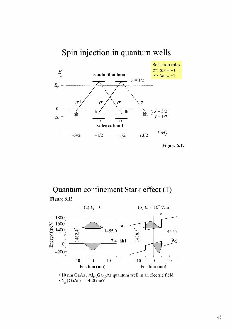
Spin injection in quantum wells
E
MJ
J = 3/2 J = 1/2
J = 1/2
�1/2,�3/2, +3/2,+1/2,
valence band
conduction band
#!
0
Eg
&+ &+ &# &#
hh hh lh lh
so so
Figure 6.12
Selection rules σ+: Δm = +1,σ�: Δm = �1
Quantum confinement Stark effect (1)
0 –10 10 Position (nm)
0 –10 10
–200
0
1400 1600 1800
Ener
gy (m
eV)
Position (nm)
(a) Ez = 0 (b) Ez = 107 V/m
1455.0 1447.9
–7.4 9.4 1462
.4
1438
.5 e1
hh1
• 10 nm GaAs / Al0.3Ga0.7As quantum well in an electric field • Eg (GaAs) = 1420 meV
Figure 6.13
46
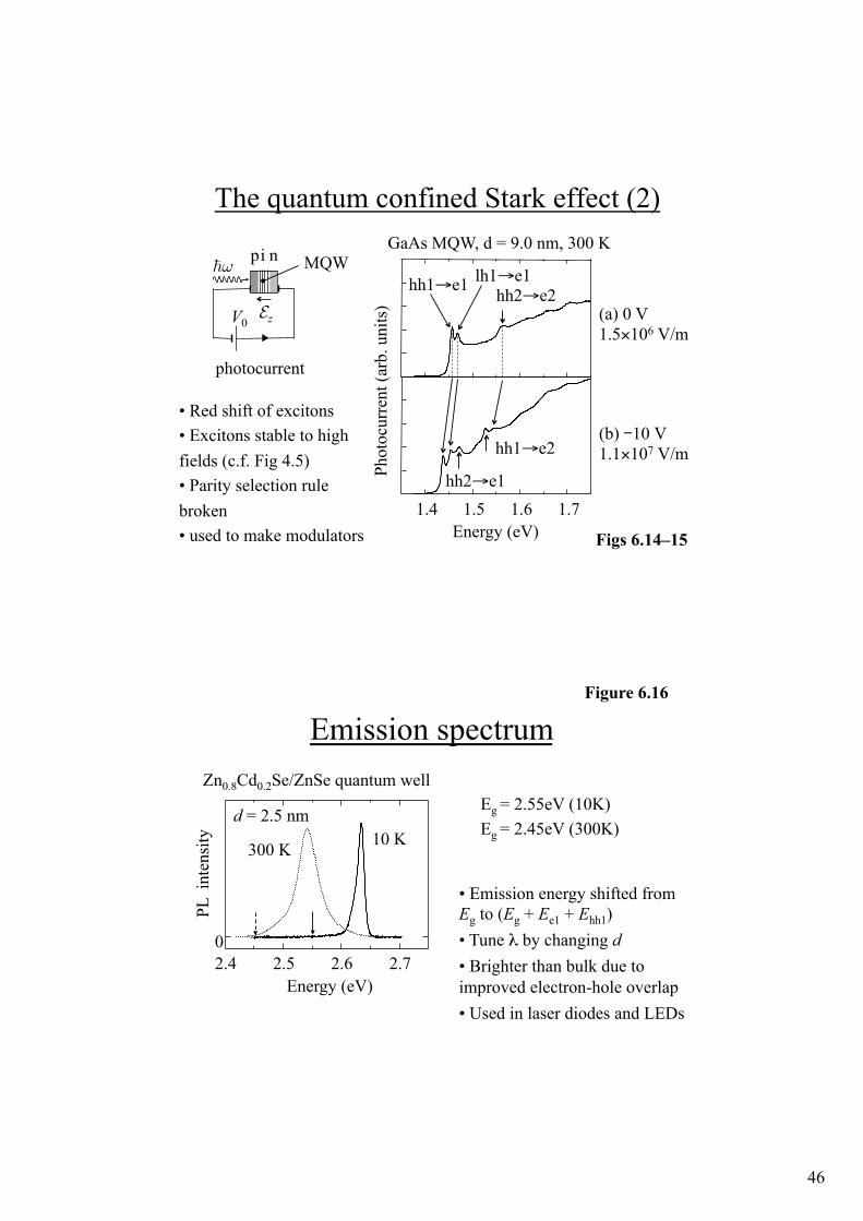
The quantum confined Stark effect (2)
MQW !% p i n
Ez V0
photocurrent
Energy (eV) 1.4 1.5 1.6 1.7
Phot
ocur
rent
(arb
. uni
ts)
(b) �10 V 1.1×10⁷ V/m
(a) 0 V 1.5×10⁶ V/m
hh1→e2
hh2→e1
hh2→e2 lh1→e1 hh1→e1
GaAs MQW, d = 9.0 nm, 300 K
Figs 6.14–15
• Red shift of excitons • Excitons stable to high fields (c.f. Fig 4.5) • Parity selection rule broken • used to make modulators
Emission spectrum Figure 6.16
2.4 2.5 2.6 2.7 0
Energy (eV)
PL i
nten
sity
300 K 10 K
Zn0.8Cd0.2Se/ZnSe quantum well
d = 2.5 nm Eg = 2.55eV (10K) Eg = 2.45eV (300K)
• Emission energy shifted from Eg to (Eg + Ee1 + Ehh1) • Tune λ by changing d • Brighter than bulk due to improved electron-hole overlap • Used in laser diodes and LEDs
47
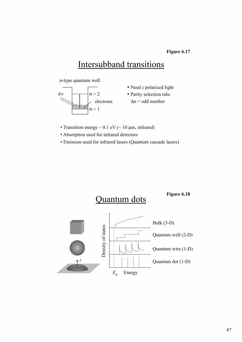
Intersubband transitions Figure 6.17
n = 1
n = 2 electrons
hν
n-type quantum well
• Transition energy ~ 0.1 eV (~ 10 µm, infrared) • Absorption used for infrared detectors • Emission used for infrared lasers (Quantum cascade lasers)
• Need z polarized light • Parity selection rule: , Δn = odd number
Quantum dots
z
Energy
Den
sity
of s
tate
s
Eg
Bulk (3-D)
Quantum well (2-D)
Quantum wire (1-D)
Quantum dot (1-D)
Figure 6.18

48
Quantum dots
E = 2π 2
2m*nx2
dx2+ny2
dy2+nz2
dz2
!
"
##
$
%
&&
(E�Eg) in units of (h 2/8d 2m*)
Den
sity
of s
tate
s
3-D
0 5 10
d Cuboid dot Spherical dot
R
E = 2
2m*Cnl2 π 2
R2
!
"##
$
%&&
C10 = 1 C11 = 1.43 C12 = 1.83 C20 = 2 "
Colloidal quantum dots
1.5 2.0 2.5 3.0 3.5
Abs
orpt
ion
(arb
. uni
ts)
Energy (eV)
CdSe 10 K
D
C
B
A
(a)
1.6 1.8 2.0 2.2 Energy (eV)
6 nm
5 nm
4 nm
CdTe 300 K
(b)
• Found in semiconductor doped glass (Colour glass filters & stained glass)
• Available commercially
Figure 6.20
49
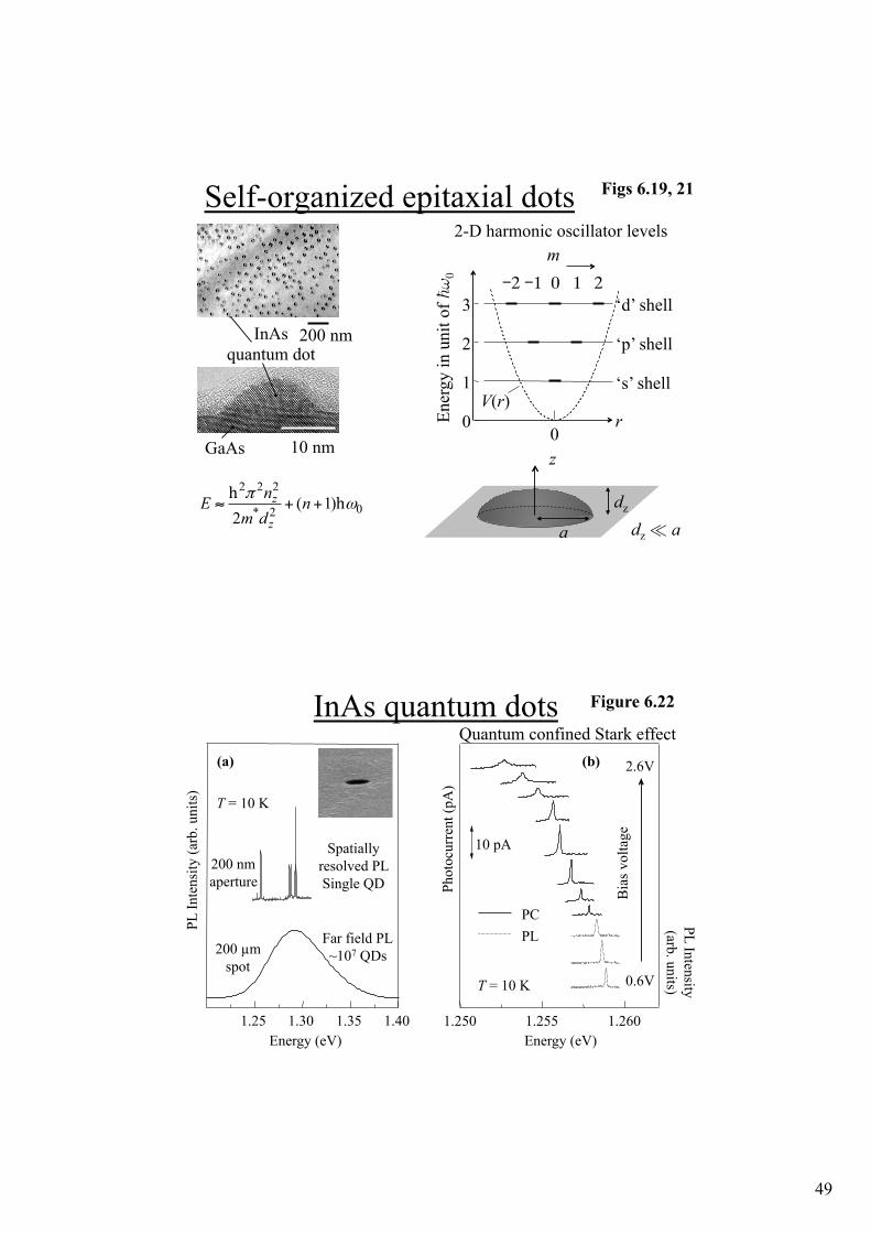
Self-organized epitaxial dots
InAs quantum dot
200 nm
10 nm GaAs
m
�2, 2,1,�1, 0,
0
1
2
3
Ener
gy in
uni
t of !% 0
0
r V(r)
‘s’ shell
‘p’ shell
‘d’ shell
2-D harmonic oscillator levels
dz ≪ a
z
a
dz
2 2 2
0* 2 ( 1)2
z
z
nE nm dπ
ω≈ + +h h
Figs 6.19, 21
InAs quantum dots Figure 6.22
1.25 1.30 1.35 1.40
200 µm spot
200 nm aperture
Spatially resolved PL Single QD
Far field PL ~107 QDs
T = 10 K
PL In
tens
ity (a
rb. u
nits
)
Energy (eV)
(a)
1.250 1.255 1.260
Phot
ocur
rent
(pA
)
Energy (eV)
PC PL
10 pA
0.6V
PL Intensity (arb. units)
2.6V
Bia
s vol
tage
(b)
T = 10 K
Quantum confined Stark effect
50
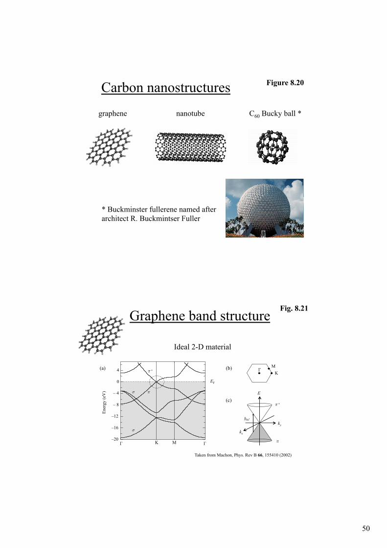
Carbon nanostructures
graphene nanotube C60 Bucky ball *
* Buckminster fullerene named after architect R. Buckmintser Fuller
Figure 8.20
Fig. 8.21
Taken from Machon, Phys. Rev B 66, 155410 (2002)
(a) (b)
ky
E
!%
M &
K
(c)
$
$ '
kx
EF
$ &
$ '
& K M –20
–16
–12
– 8
– 4
0
4
Ener
gy (e
V)
&
&
Graphene band structure
Ideal 2-D material
51
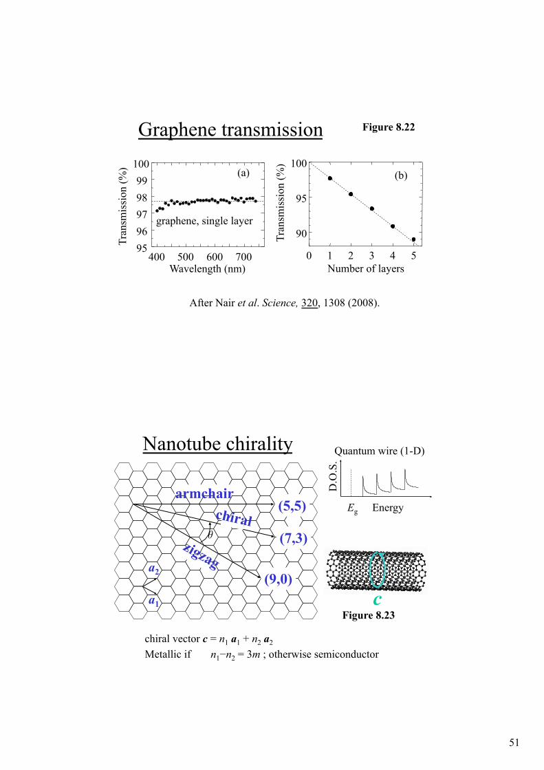
Figure 8.22 Graphene transmission
After Nair et al. Science, 320, 1308 (2008).
0 1 2 3 4 5
90
95
100
Tran
smis
sion
(%)
Number of layers
(b)
400 500 600 700 95 96 97 98 99
100
Tran
smis
sion
(%)
Wavelength (nm)
(a)
graphene, single layer
a1
a2
armchair
zigzag
(5,5)
(9,0)
(7,3) "
chiral
Figure 8.23
Nanotube chirality
chiral vector c = n1 a1 + n2 a2
Metallic if n1−n2 = 3m ; otherwise semiconductor
c
Energy
D.O
.S.
Eg
Quantum wire (1-D)
52
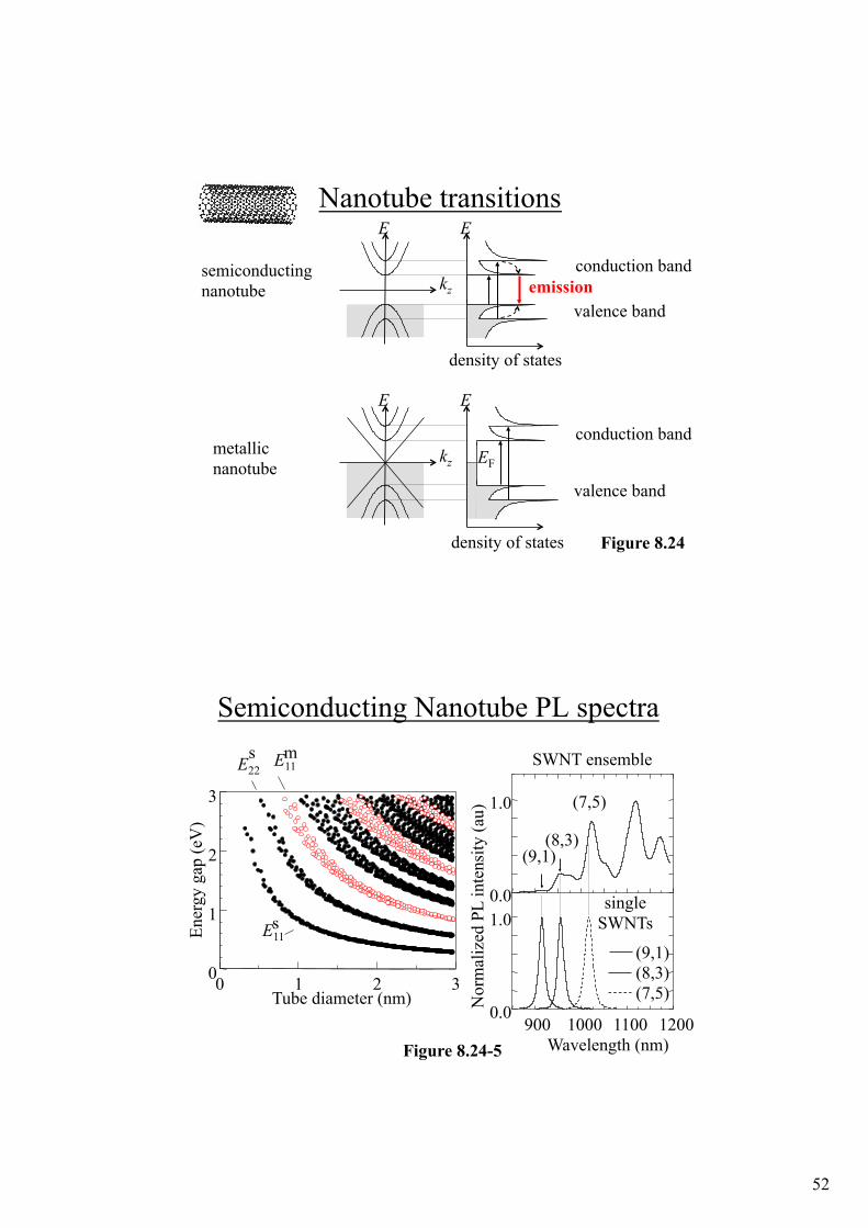
Figure 8.24
E E
density of states
kz conduction band
valence band
semiconducting nanotube
E E
kz conduction band
valence band
density of states
metallic nanotube EF
Nanotube transitions
emission
Figure 8.24-5
0 1 2 3 0
1
2
3
Ener
gy g
ap (e
V)
Tube diameter (nm)
E11 m
E11 s
E22 s
900 1000 1100 1200 0.0
1.0
Nor
mal
ized
PL
inte
nsity
(au)
Wavelength (nm)
0.0
1.0
(9,1)
single SWNTs
(7,5)
(8,3)
SWNT ensemble
(9,1) (8,3) (7,5)
Semiconducting Nanotube PL spectra
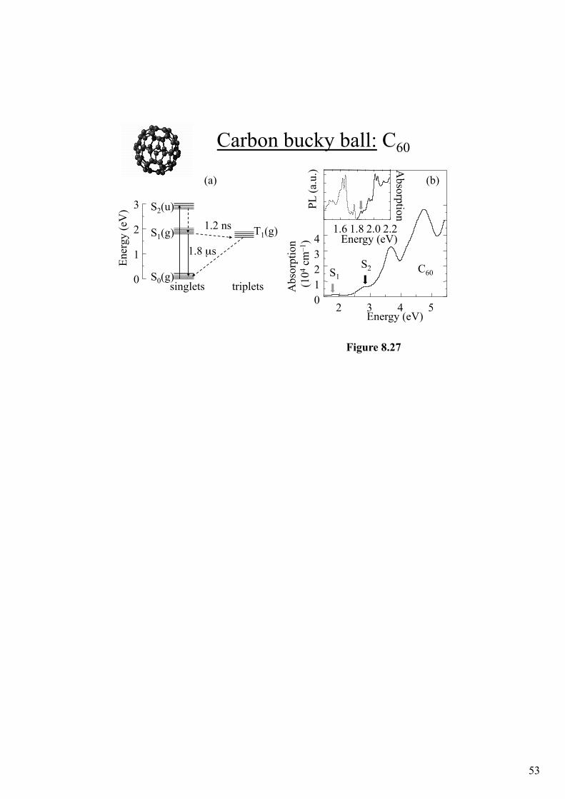
53
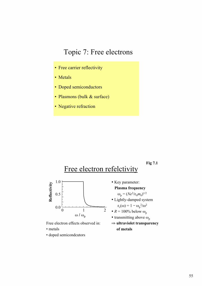
Figure 8.27
0
1
2
3
Ener
gy (e
V)
singlets triplets S0(g)
S1(g)
S2(u)
T1(g) 1.2 ns
1.8 µs
(a) (b)
Energy (eV) 2 3 4 5
0 1 2 3 4
Abs
orpt
ion
(104 c
m–1
)
1.6 1.8 2.0 2.2
Absorption
Energy (eV)
PL (a
.u.)
S1 S2 C60
Carbon bucky ball: C60

54
55
Topic 7: Free electrons
• Free carrier reflectivity
• Metals
• Doped semiconductors
• Plasmons (bulk & surface)
• Negative refraction
Free electron refelctivity Fig 7.1
ω / ωp
Ref
lect
ivity
0 1 2 0.0
0.5
1.0
Free electron effects observed in: • metals • doped semicondcutors
• Key parameter: Plasma frequency , ωp = (Ne2/ε0m0)1/2 • Lightly-damped system, εr(ω) = 1 � ωp
2/ω2,
• R = 100% below ωp
• transmitting above ωp ⇒ ultraviolet transparency of metals
56
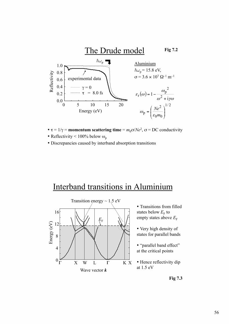
The Drude model Fig 7.2
( )
2/1
00
2p
2
2p
r i
1
!!"
#$$%
&=
+−=
mNeε
ω
γωω
ωωε
• τ = 1/γ = momentum scattering time = m0σ/Ne2, σ = DC conductivity
• Reflectivity < 100% below ωp • Discrepancies caused by interband absorption transitions
0 5 10 15 20 0.0 0.2 0.4 0.6 0.8 1.0
Energy (eV)
Ref
lect
ivity
experimental data
τ = 8.0 fs γ = 0
!%p Aluminium !%p = 15.8 eV, σ = 3.6 × 10⁷ Ω–1 m–1
Interband transitions in Aluminium
Fig 7.3
• Transitions from filled states below EF to empty states above EF • Very high density of states for parallel bands • “parallel band effect” at the critical points • Hence reflectivity dip at 1.5 eV,
Transition energy ~ 1.5 eV
Ener
gy (e
V)
Γ, X W L Γ, K X 0
4
8
12
16
Wave vector k
EF
57
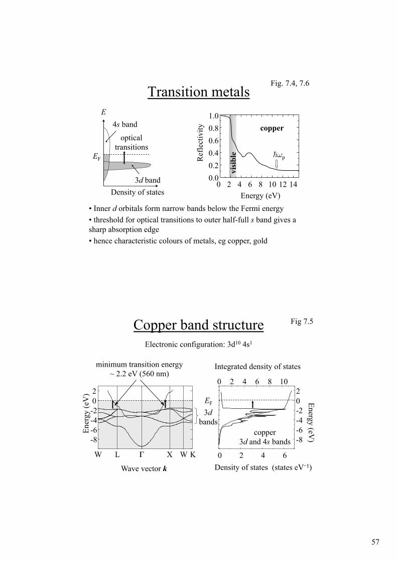
Transition metals
Density of states
E
3d band
4s band
EF
optical transitions
0 2 4 6 8 10 12 14 0.0 0.2 0.4 0.6 0.8 1.0
copper
Energy (eV) R
efle
ctiv
ity
!%p
visi
ble
Fig. 7.4, 7.6
• Inner d orbitals form narrow bands below the Fermi energy • threshold for optical transitions to outer half-full s band gives a sharp absorption edge • hence characteristic colours of metals, eg copper, gold
Copper band structure
W L Γ, X W K
-8 -6 -4 -2 0 2
Ener
gy (e
V)
0 2 4 6
Energy (eV)
Density of states (states eV�1)
0 2 4 6 8 10
-8 -6 -4 -2 0 2
Integrated density of states
Wave vector k
EF
copper 3d and 4s bands
3d bands
minimum transition energy ~ 2.2 eV (560 nm)
Fig 7.5
Electronic configuration: 3d10 4s1
58
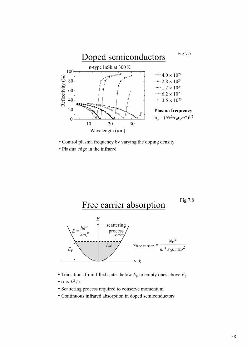
Doped semiconductors
10 20 30 0
20
40
60
80
100
Wavelength (µm)
Ref
lect
ivity
(%) 4.0 × 1024
2.8 × 1024 1.2 × 1024 6.2 × 10²³ 3.5 × 10²³
n-type InSb at 300 K
Plasma frequency ,ωp = (Ne2/ε0εrm*)1/2
• Control plasma frequency by varying the doping density • Plasma edge in the infrared
Fig 7.7
Free carrier absorption
k
E
EF
scattering process
!%
E = !k 2
2me *
• Transitions from filled states below EF to empty ones above EF • α ∝ λ2 / τ • Scattering process required to conserve momentum • Continuous infrared absorption in doped semiconductors
20
2carrier free
* τωεα
ncmNe
=
Fig 7.8
59
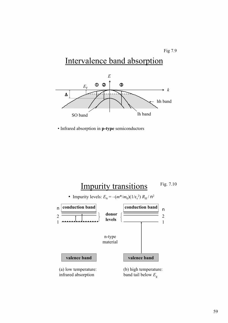
Intervalence band absorption
k
E
EF !!"! #$
hh band
lh band SO band
Δ,
• Infrared absorption in p-type semiconductors
Fig 7.9
Impurity transitions Fig. 7.10
conduction band
valence band
1 2
n donor levels
conduction band
valence band
1 2 n
(a) low temperature: infrared absorption
(b) high temperature: band tail below Eg
• Impurity levels: En = –(m*/m0)(1/εr2) RH / n2
n-type material
60
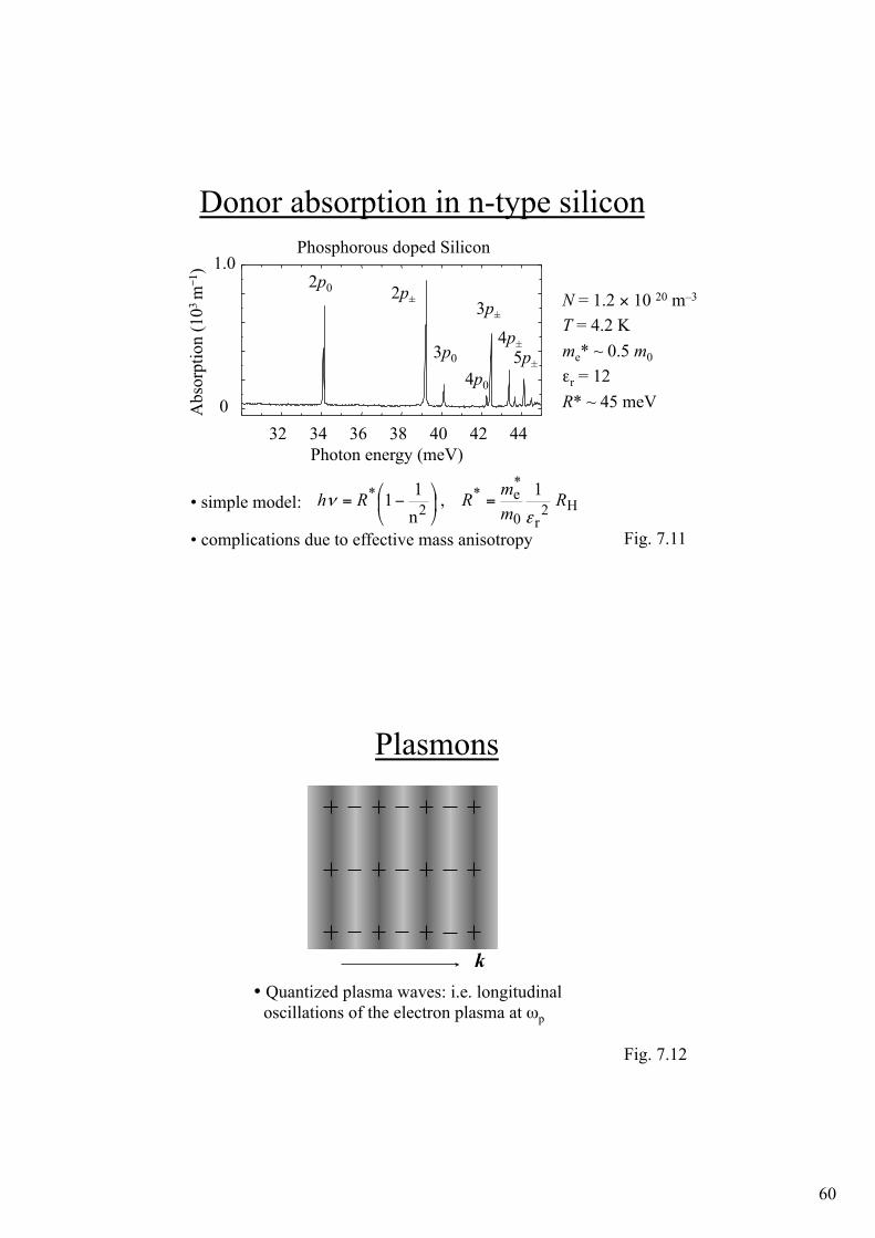
Donor absorption in n-type silicon
32 34 36 38 40 42 44 0
1.0
Photon energy (meV)
Abs
orpt
ion
(103
m�1 )
2p0
4p0 3p0
2p± 3p±
4p± 5p±
Phosphorous doped Silicon
H2r0
*e*
2* 1 ,
n11 R
mmRRh
εν =#
$
%&'
( −=
Fig. 7.11
N = 1.2 × 10 20 m–3 T = 4.2 K me* ~ 0.5 m0 εr = 12 R* ~ 45 meV
• simple model:
• complications due to effective mass anisotropy
k
Plasmons
• Quantized plasma waves: i.e. longitudinal oscillations of the electron plasma at ωp
Fig. 7.12
61
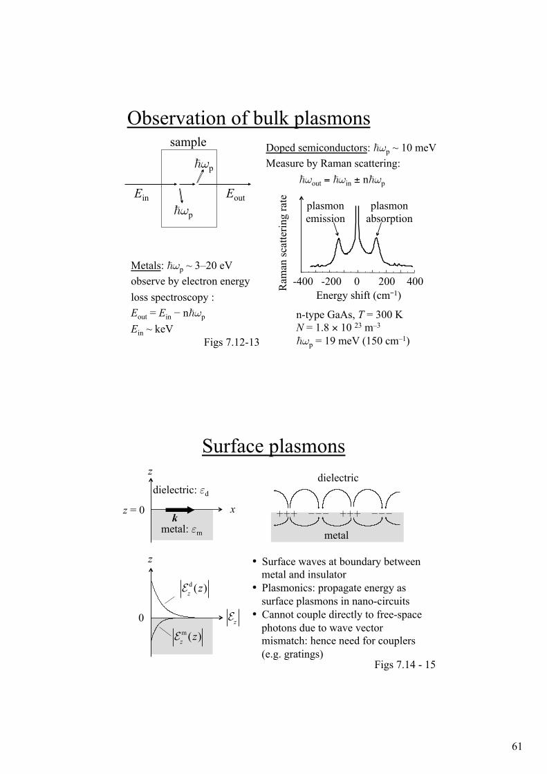
Observation of bulk plasmons
-400 -200 0 200 400 Energy shift (cm�1)
plasmon absorption
plasmon emission
Ram
an sc
atte
ring
rate
Metals: !%p ~ 3–20 eV observe by electron energy loss spectroscopy : Eout = Ein − n!%p
Ein ~ keV
Doped semiconductors: !%p ~ 10 meV Measure by Raman scattering:
!%out = !%in ± n!%p
n-type GaAs, T = 300 K N = 1.8 × 10 23 m–3 !%p = 19 meV (150 cm–1)
Ein Eout !%p
sample
!%p
Figs 7.12-13
Surface plasmons
0
z
dielectric: (d
x
metal: (m
z = 0
z
k
• Surface waves at boundary between metal and insulator
• Plasmonics: propagate energy as surface plasmons in nano-circuits
• Cannot couple directly to free-space photons due to wave vector mismatch: hence need for couplers (e.g. gratings)
+++ ### +++ ###
metal
dielectric
Figs 7.14 - 15
Ezd (z)
Ezm(z)
Ez
62
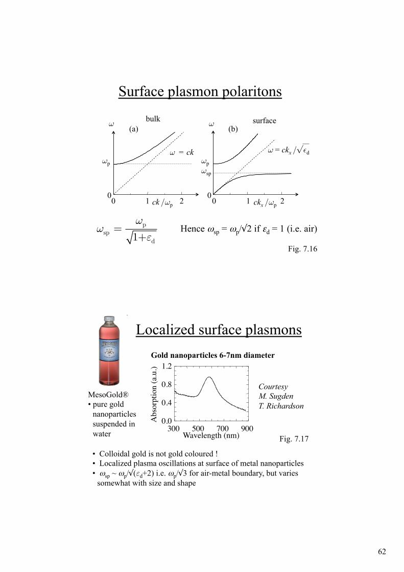
Surface plasmon polaritons
0 1 2 0 1 2 ck /%p ckx /%p
%p %p
0 0
% %
% = ck
(a) (b)
%sp
% = ckx /(εd
bulk surface
psp
d1+!
!"
= Hence ωsp = ωp/√2 if εd = 1 (i.e. air)
Fig. 7.16
Localized surface plasmons
300! 500! 700! 900!0.0!
0.4!
0.8!
1.2!
Abs
orpt
ion
(a.u
.)!
Wavelength (nm)!
Gold nanoparticles 6-7nm diameter
Courtesy M. Sugden T. Richardson
• Colloidal gold is not gold coloured ! • Localized plasma oscillations at surface of metal nanoparticles • ωsp ~ ωp/√((d+2) i.e. ωp/√3 for air-metal boundary, but varies
somewhat with size and shape
MesoGold® • pure gold
nanoparticles suspended in water Fig. 7.17
63
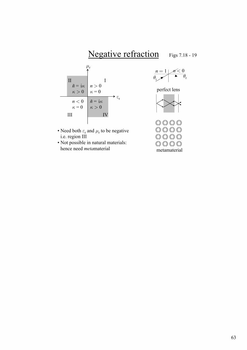
Negative refraction
)r
µr
n > 0 ) = 0
n < 0 ) = 0
ñ = i) ) > 0
I II
III IV
ñ = i) ) > 0
"i "r
n < 0 n = 1
perfect lens
metamaterial
• Need both (r and µr to be negative i.e. region III
• Not possible in natural materials: hence need metamaterial
Figs 7.18 - 19

64
65
Topic 8: Phonons (Chapter 10)
• Infrared active phonons
• Reststrahlen
• Inelastic light scattering
$ Raman scattering
• Phonon lifetimes
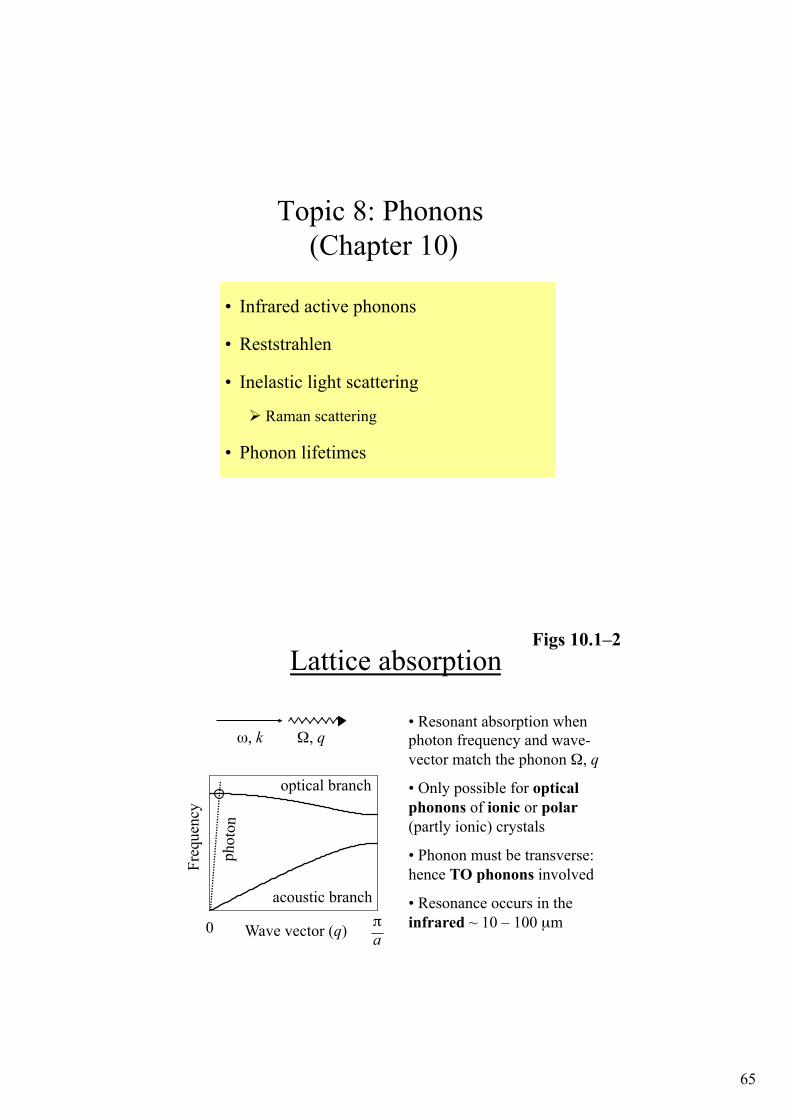
Lattice absorption Figs 10.1–2
ω, k Ω, q
Wave vector (q)
Freq
uenc
y
acoustic branch
optical branch
π a
0
phot
on
• Resonant absorption when photon frequency and wave-vector match the phonon Ω, q
• Only possible for optical phonons of ionic or polar (partly ionic) crystals
• Phonon must be transverse: hence TO phonons involved
• Resonance occurs in the infrared ~ 10 – 100 µm
66
TO phonon resonance
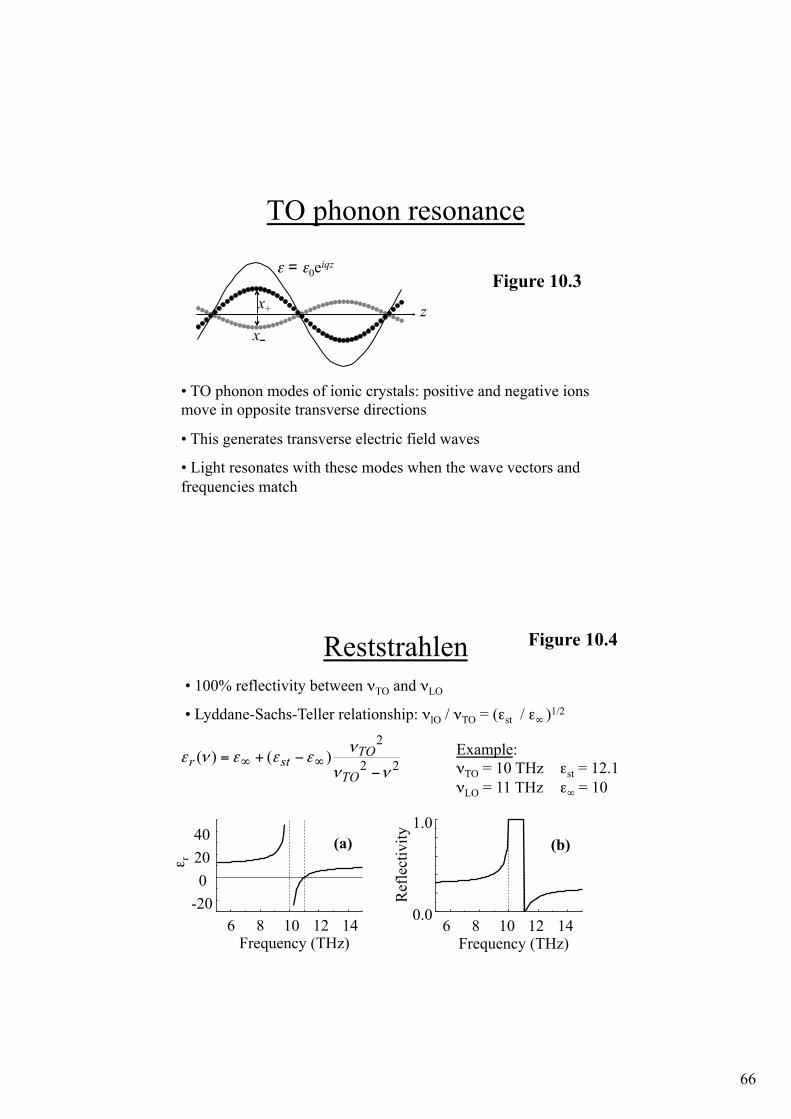
ε = ε0eiqz
x+
x� z
Figure 10.3
• TO phonon modes of ionic crystals: positive and negative ions move in opposite transverse directions
• This generates transverse electric field waves
• Light resonates with these modes when the wave vectors and frequencies match
Reststrahlen
6 8 10 12 14 -20 0
20 40 (a)
ε r
Frequency (THz) 6 8 10 12 14
0.0
1.0 (b)
Frequency (THz)
Ref
lect
ivity
Figure 10.4
22
2)()(
νν
νεεενε
−−+= ∞∞
TO
TOstr
Example: νTO = 10 THz εst = 12.1 νLO = 11 THz ε∞ = 10
• 100% reflectivity between νTO and νLO
• Lyddane-Sachs-Teller relationship: νlO / νTO = (εst / ε∞ )1/2
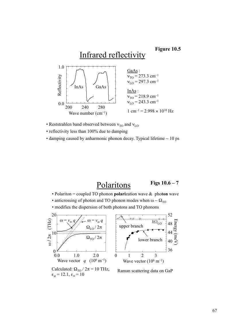
67
Infrared reflectivity
200 240 280 0.0
1.0
GaAs InAs
Ref
lect
ivity
Wave number (cm�1)
Figure 10.5
• Reststrahlen band observed between νTO and νLO • reflectivity less than 100% due to damping • damping caused by anharmonic phonon decay. Typical lifetime ~ 10 ps
GaAs : νTO = 273.3 cm–1
νLO = 297.3 cm–1
InAs : νTO = 218.9 cm–1
νLO = 243.3 cm–1
1 cm–1 = 2.998 × 10¹⁰ Hz
Polaritons
0.0 1.0 2.0 0
10
20
Wave vector q (106 m�1)
ω /
2π
(TH
z)
ΩTO / 2π
ΩLO / 2π ω = vst q ω = v∞ q
Figs 10.6 – 7
Raman scattering data on GaP
!$LO
lower branch
upper branch
0 1 2 3 36
40
44
48
52 Energy (meV
)
Wave vector (106 m�1)
Calculated: ΩTO / 2π = 10 THz, εst = 12.1, ε∞ = 10
• Polariton = coupled TO phonon polarization wave & photon wave • anticrossing of photon and TO phonon modes when ω ~ ΩTO • modifies the dispersion of both photons and TO phonons
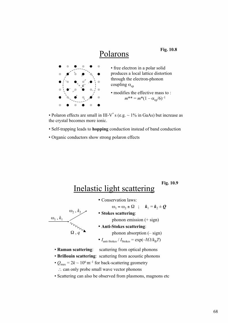
68
Polarons Fig. 10.8
e�
• free electron in a polar solid produces a local lattice distortion through the electron-phonon coupling αep
• modifies the effective mass to : m** = m*(1 – αep/6)–1
• Polaron effects are small in III-V�s (e.g. ~ 1% in GaAs) but increase as the crystal becomes more ionic.
• Self-trapping leads to hopping conduction instead of band conduction
• Organic conductors show strong polaron effects
Inelastic light scattering Fig. 10.9
ω1 , k1 ω2 , k2
Ω , q
• Conservation laws: ,ω1 = ω2 ± Ω ; k1 = k2 ± Q
• Stokes scattering: phonon emission (+ sign)
• Anti-Stokes scattering: phonon absorption (– sign)
• Ianti-Stokes / IStokes = exp(–!$/kBT)
• Raman scattering: scattering from optical phonons • Brillouin scattering: scattering from acoustic phonons • Qmax = 2k ~ 106 m–1 for back-scattering geometry ∴ can only probe small wave vector phonons • Scattering can also be observed from plasmons, magnons etc
69
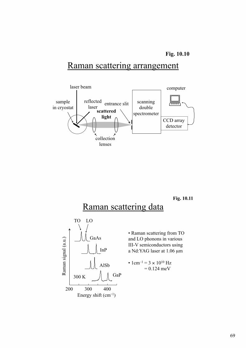
Raman scattering arrangement Fig. 10.10
sample in cryostat
collection lenses
laser beam
reflected laser
scattered light
CCD array detector
scanning double
spectrometer
entrance slit
computer
#
Raman scattering data Fig. 10.11
200 300 400
GaP
AlSb
InP
GaAs
300 K Ram
an si
gnal
(a.u
.)
Energy shift (cm�1)
• Raman scattering from TO and LO phonons in various III-V semiconductors using a Nd:YAG laser at 1.06 µm • 1cm–1 = 3 × 10¹⁰ Hz = 0.124 meV
TO LO
70
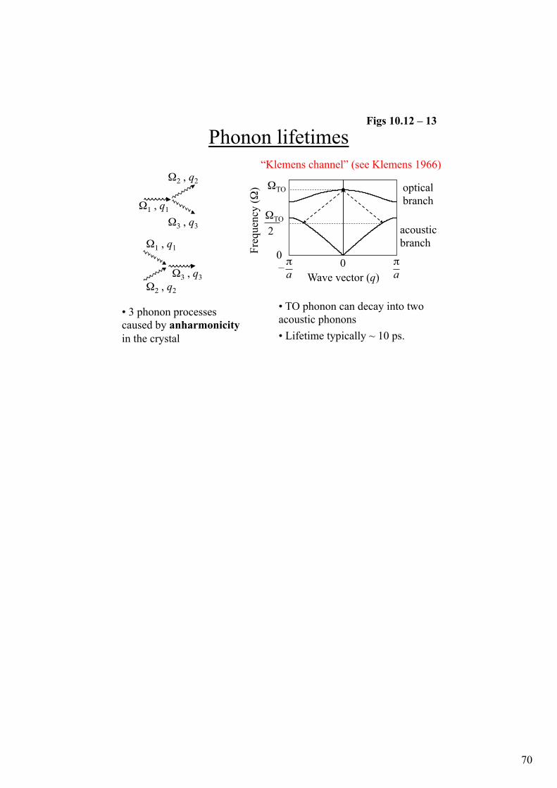
Phonon lifetimes
Ω1 , q1
Ω2 , q2
Ω3 , q3
Ω1 , q1
Ω2 , q2 Ω3 , q3
Figs 10.12 – 13
• 3 phonon processes caused by anharmonicity in the crystal
Wave vector (q)
Freq
uenc
y (Ω
)
acoustic branch
optical branch
0 π a
ΩTO
ΩTO
2
0 π a
• TO phonon can decay into two acoustic phonons • Lifetime typically ~ 10 ps.
“Klemens channel” (see Klemens 1966)
71
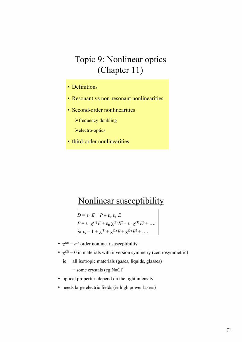
Topic 9: Nonlinear optics (Chapter 11)
• Definitions
• Resonant vs non-resonant nonlinearities
• Second-order nonlinearities
$ frequency doubling
$ electro-optics
• third-order nonlinearities
Nonlinear susceptibility D = ε0 E + P ≡ ε0 εr E
P = ε0 χ(1) E + ε0 χ(2) E2 + ε0 χ(3) E3 + ….
% εr = 1 + χ(1) + χ(2) E + χ(3) E2 + ….
• χ(n) = nth order nonlinear susceptibility,
• χ(2) = 0 in materials with inversion symmetry (centrosymmetric)
ie: all isotropic materials (gases, liquids, glasses)
+ some crystals (eg NaCl)
• optical properties depend on the light intensity
• needs large electric fields (ie high power lasers)
72
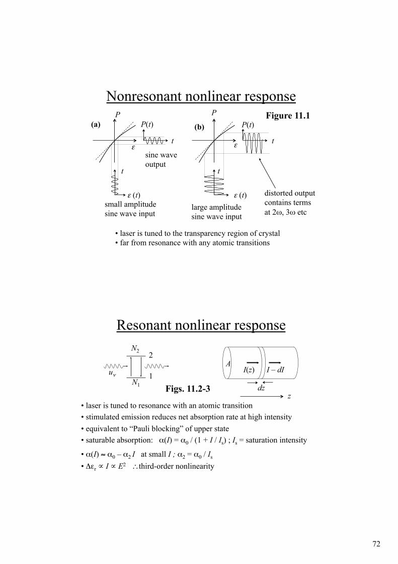
Nonresonant nonlinear response P
ε,
ε (t),
t,
t
P(t) P
ε,
ε (t),
t,
t
P(t) (a) (b) Figure 11.1
distorted output contains terms at 2ω, 3ω etc
small amplitude sine wave input
large amplitude sine wave input
sine wave output
• laser is tuned to the transparency region of crystal • far from resonance with any atomic transitions
Resonant nonlinear response
Figs. 11.2-3
N2
N1
2
1 uν A
z dz
I(z) I – dI
• laser is tuned to resonance with an atomic transition • stimulated emission reduces net absorption rate at high intensity • equivalent to “Pauli blocking” of upper state • saturable absorption: α(I) = α0 / (1 + I / Is) ; Is = saturation intensity
• α(I) ≈ α0 – α2 I at small I ; α2 = α0 / Is
• Δεr ∝ I ∝ E2 ∴third-order nonlinearity

73
Second order nonlinear effects
ω2
ω1
ω1+ω2
Process Input Ouptut Frequency mixing ω1, ω2 , , ω1 + ω2 Frequency doubling ω, ω 2ω,Down conversion ω1 ω2, ω1 � ω2,
�ω2
ω1
ω1�ω2 (b)
Fig. 11.4
(a)
Pi(2) = ε0 Σjk χ(2)
ijk Ej Ek χ(2) = 0 in centrosymmetric crystals
Phase matching
• Phase matching condition: 2kω = k2ω (conservation of momentum) ⇒ 2× n(ω) ω / c = n(2ω) 2ω / c ⇒ n(ω) = n(2ω) • not usually possible due to dispersion. • use a birefringent crystal with optic axis at angle θ :$
kω 2ω
χ(2) ω
k2ω
2o
2
2e
2
2o )2(
cos
)2(
sin
)(
1
ω
θ
ω
θ
ω nnn+=
θ
74
2ω,
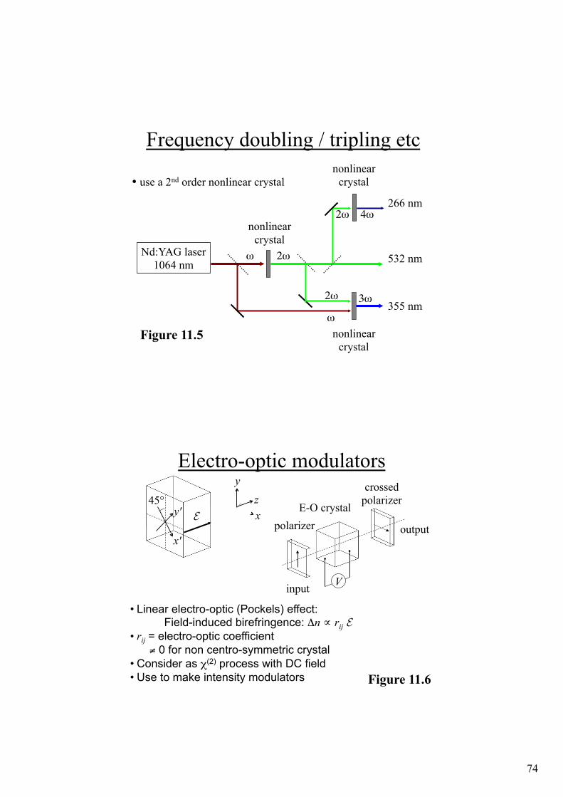
Frequency doubling / tripling etc
Figure 11.5
Nd:YAG laser 1064 nm
nonlinear crystal
532 nm
355 nm
266 nm
2ω,
4ω,
ω,
ω,
2ω, 3ω,
nonlinear crystal
nonlinear crystal
• use a 2nd order nonlinear crystal
Electro-optic modulators
z x
y
x'
y' 45°
E polarizer
crossed polarizer E-O crystal
V input
output
• Linear electro-optic (Pockels) effect: Field-induced birefringence: Δn ∝ rij E
• rij = electro-optic coefficient ≠ 0 for non centro-symmetric crystal
• Consider as χ(2) process with DC field • Use to make intensity modulators Figure 11.6
75
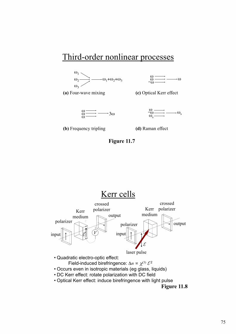
Third-order nonlinear processes
Figure 11.7
(b) Frequency tripling
ω,ω,ω,
3ω,
(c) Optical Kerr effect
ω ω �ω
ω
(a) Four-wave mixing
ω1 ω2 ω3
ω1+ω2+ω3
(d) Raman effect
ω �ω ωs
ωs
Kerr cells
E
polarizer
crossed polarizer Kerr
medium
input
output
V
polarizer
crossed polarizer Kerr
medium
input
output
laser pulse
E
Figure 11.8
• Quadratic electro-optic effect: Field-induced birefringence: Δn ∝ χ(3) E 2
• Occurs even in isotropic materials (eg glass, liquids) • DC Kerr effect: rotate polarization with DC field • Optical Kerr effect: induce birefringence with light pulse
76
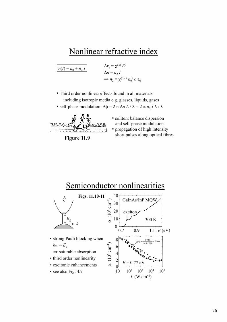
Nonlinear refractive index
Figure 11.9
Δεr = χ(3) E2
Δn = n2 I ⇒ n2 = χ(3) / n0
2 c ε0
n(I) = n0 + n2 I
• Third order nonlinear effects found in all materials including isotropic media e.g. glasses, liquids, gases • self-phase modulation: Δφ = 2 π Δn L / λ = 2 π n2 I L / λ,
• soliton: balance dispersion and self-phase modulation • propagation of high intensity short pulses along optical fibres
Semiconductor nonlinearities Figs. 11.10-11
k
E
Eg
10 102 103 104 105 0 2 4 6 8
α (
103 c
m�1 )
I (W cm�2)
α( )/
II
=+
+6700
1 2902000
E = 0.77 eV
0.7 0.9 1.1 0
10
20
30
40
α (
103 c
m�1 )
E (eV)
GaInAs/InP MQW
exciton
300 K
• strong Pauli blocking when !% ~ Eg
⇒ saturable absorption • third order nonlinearity • excitonic enhancements • see also Fig. 4.7
77
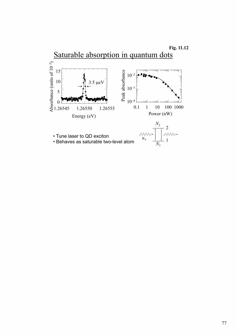
Saturable absorption in quantum dots Fig. 11.12
0.1 1 10 100 1000 10–4
10–3
10–2
Power (nW)
Pea
k ab
sorb
ance
1.26545 1.26550 1.26555 0
5
10
15
Energy (eV)
Abs
orba
nce
(uni
ts o
f 10–3
)
3.5 µeV
• Tune laser to QD exciton • Behaves as saturable two-level atom
N2
N1
2
1 uν